US20020005562A1 - Semiconductor power integrated circuit and method for fabricating the same - Google Patents
Semiconductor power integrated circuit and method for fabricating the sameDownload PDFInfo
- Publication number
- US20020005562A1 US20020005562A1US09/865,004US86500401AUS2002005562A1US 20020005562 A1US20020005562 A1US 20020005562A1US 86500401 AUS86500401 AUS 86500401AUS 2002005562 A1US2002005562 A1US 2002005562A1
- Authority
- US
- United States
- Prior art keywords
- oxide layer
- teos
- recited
- forming
- layer
- Prior art date
- Legal status (The legal status is an assumption and is not a legal conclusion. Google has not performed a legal analysis and makes no representation as to the accuracy of the status listed.)
- Granted
Links
Images


Classifications
- H—ELECTRICITY
- H10—SEMICONDUCTOR DEVICES; ELECTRIC SOLID-STATE DEVICES NOT OTHERWISE PROVIDED FOR
- H10D—INORGANIC ELECTRIC SEMICONDUCTOR DEVICES
- H10D30/00—Field-effect transistors [FET]
- H—ELECTRICITY
- H10—SEMICONDUCTOR DEVICES; ELECTRIC SOLID-STATE DEVICES NOT OTHERWISE PROVIDED FOR
- H10D—INORGANIC ELECTRIC SEMICONDUCTOR DEVICES
- H10D86/00—Integrated devices formed in or on insulating or conducting substrates, e.g. formed in silicon-on-insulator [SOI] substrates or on stainless steel or glass substrates
- H10D86/01—Manufacture or treatment
- H—ELECTRICITY
- H01—ELECTRIC ELEMENTS
- H01L—SEMICONDUCTOR DEVICES NOT COVERED BY CLASS H10
- H01L21/00—Processes or apparatus adapted for the manufacture or treatment of semiconductor or solid state devices or of parts thereof
- H01L21/70—Manufacture or treatment of devices consisting of a plurality of solid state components formed in or on a common substrate or of parts thereof; Manufacture of integrated circuit devices or of parts thereof
- H01L21/71—Manufacture of specific parts of devices defined in group H01L21/70
- H01L21/76—Making of isolation regions between components
- H01L21/762—Dielectric regions, e.g. EPIC dielectric isolation, LOCOS; Trench refilling techniques, SOI technology, use of channel stoppers
- H01L21/7624—Dielectric regions, e.g. EPIC dielectric isolation, LOCOS; Trench refilling techniques, SOI technology, use of channel stoppers using semiconductor on insulator [SOI] technology
- H01L21/76264—SOI together with lateral isolation, e.g. using local oxidation of silicon, or dielectric or polycristalline material refilled trench or air gap isolation regions, e.g. completely isolated semiconductor islands
- H—ELECTRICITY
- H10—SEMICONDUCTOR DEVICES; ELECTRIC SOLID-STATE DEVICES NOT OTHERWISE PROVIDED FOR
- H10D—INORGANIC ELECTRIC SEMICONDUCTOR DEVICES
- H10D86/00—Integrated devices formed in or on insulating or conducting substrates, e.g. formed in silicon-on-insulator [SOI] substrates or on stainless steel or glass substrates
- H10D86/201—Integrated devices formed in or on insulating or conducting substrates, e.g. formed in silicon-on-insulator [SOI] substrates or on stainless steel or glass substrates the substrates comprising an insulating layer on a semiconductor body, e.g. SOI
- H—ELECTRICITY
- H01—ELECTRIC ELEMENTS
- H01L—SEMICONDUCTOR DEVICES NOT COVERED BY CLASS H10
- H01L21/00—Processes or apparatus adapted for the manufacture or treatment of semiconductor or solid state devices or of parts thereof
- H01L21/70—Manufacture or treatment of devices consisting of a plurality of solid state components formed in or on a common substrate or of parts thereof; Manufacture of integrated circuit devices or of parts thereof
- H01L21/71—Manufacture of specific parts of devices defined in group H01L21/70
- H01L21/76—Making of isolation regions between components
- H01L21/762—Dielectric regions, e.g. EPIC dielectric isolation, LOCOS; Trench refilling techniques, SOI technology, use of channel stoppers
- H01L21/7624—Dielectric regions, e.g. EPIC dielectric isolation, LOCOS; Trench refilling techniques, SOI technology, use of channel stoppers using semiconductor on insulator [SOI] technology
- H01L21/76264—SOI together with lateral isolation, e.g. using local oxidation of silicon, or dielectric or polycristalline material refilled trench or air gap isolation regions, e.g. completely isolated semiconductor islands
- H01L21/76283—Lateral isolation by refilling of trenches with dielectric material
Definitions
- the present inventionrelates to a semiconductor power integrated circuit; and, more particularly, to a semiconductor power integrated circuit and a method for fabricating the same having a trench isolation, in which a field oxide layer, a gate oxide layer and a diode insulating layer are simultaneously formed together with a trench filling, thereby reducing processing steps and obtaining a low on-resistance.
- ICsSemiconductor power integrated circuits for use in a high voltage of 100V to 500V have been used as driver ICs in such as step motors, FED (field emission display) and PDP (plasma display panel).
- FEDfield emission display
- PDPplasma display panel
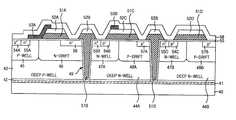
- FIG. 1a conventional trench filling technology used for isolation in the semiconductor power device will be described below.
- a buried oxide layer 11 and a P-epi (epitaxial) layer 12are sequentially formed on an N-type silicon substrate 10 .
- a deep P-well region 13 and deep N-well regions 14 A and 14 Bare formed on the P-epi layer 12 .
- an ion implantationis performed to form a P-well region 18 , an N-drift region 19 , N-well regions 20 A and 20 B and P-drift regions 21 A and 21 B.
- the deep P-well region 13 and the deep N-well regions 14 A and 14 Bare selectively etched to form a trench 15 to thereby expose the buried oxide layer 11 .
- a TEOS (tetra-ethyl-ortho-silicate) -oxide layer 16is formed on a whole surface of the semiconductor structure after forming the trench 15 and the polysilicon layer 17 is then formed on the TEOS-oxide layer 16 to thereby fill the trench 15 . Then, an etch back or a chemical mechanical polishing (CMP) is performed to planarize a surface of an entire structure after filling the trench 15 . Thereafter, a local oxidation of silicon (LOCOS) process is performed at a temperature of about 1000° C. for a long time to form a field oxide layer 23 , a trench isolation layer 22 , a gate oxide layer 24 and a diode insulating layer 25 .
- LOClocal oxidation of silicon
- Gate electrodes 26 and 27are formed on the field oxide layer 23 and the gate oxide layer 24 .
- a n + source regions 28 A to 28 C, p + source regions 29 A to 29 C, n + drain region 30 , and p + drain regions 31 A and 31 Bare formed on the P-well region 18 , the N-drift region 19 , the N-well regions 20 A and 20 B and the P-drift regions 21 A and 21 B by an ion implantation of impurities.
- a breakdown voltage and an on-resistanceare controlled by the deep N-well regions 14 A and 14 B and the P-drift regions 21 A and 21 B, wherein the deep N-well regions 14 A and 14 B are formed on the P-epi layer 12 having a high resistivity. That is, a breakdown voltage of a vertical direction is determined by a thickness and impurity concentration of the P-epi layer 12 and a depth and impurity concentration of the P-drift regions 21 A and 21 B. A breakdown voltage of a horizontal direction is determined by a distance between the p + drain regions 31 A and 31 B and the p + source regions 29 B and 29 C.
- the voltage breakdownoccurs at a drain edge, and in case where the impurity concentration of the P-drift regions 21 A and 21 B is high, the voltage breakdown occurs at a gate edge.
- a method for fabricating a semiconductor power integrated circuitcomprising the steps of: a) forming a semiconductor structure having at least one active region, wherein an active region includes a well region for forming a channel and a source, and a drift region for forming a drain region; b) forming a trench for isolation of the active regions, wherein the trench has a predetermined depth from a surface of the semiconductor structure; c) forming a first TEOS-oxide layer inside the trench and above the semiconductor structure, wherein the first TEOS-oxide layer has a predetermined thickness from the surface of the semiconductor device; d) forming a second TEOS-oxide layer on the first TEOS-oxide layer, wherein a thickness of the second TEOS-oxide layer is smaller than that of the first TEOS-oxide layer; and e) performing a selective etching to the first and second TEOS-oxide layers, to thereby simultaneously form
- a semiconductor power integrated circuitcomprising; a) a semiconductor structure having a trench with a predetermined depth from a surface of the semiconductor structure, wherein the semiconductor structure includes an active region having a well region for forming a channel and a source, and a drift region for forming a drain region; b) a trench isolation layer pattern including a first oxide layer and a second oxide layer, wherein the first oxide layer fills inside the trench and has a predetermined thickness from the surface of the semiconductor structure, and wherein the second oxide layer is formed on the first oxide layer and has a predetermined thickness smaller than the second oxide layer; c) a field oxide layer pattern including a third oxide layer and a fourth oxide layer, wherein the third oxide layer is simultaneously formed with the same layer as the first oxide layer of the field oxide layer pattern and has a predetermined thickness from a surface of the semiconductor structure, and wherein the fourth oxide layer is simultaneously formed with the same layer as the second oxide layer of the field oxide layer of
- FIG. 1is a cross-sectional diagram illustrating a semiconductor power IC in accordance with the prior art
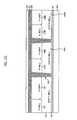
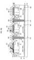
- FIGS. 2A to 2 Iare cross-sectional diagrams illustrating a semiconductor power IC in accordance with the present invention.
- FIG. 3is a graph illustrating a current/voltage characteristic of a semiconductor power IC.
- FIGS. 2A to 2 Ga semiconductor power integrated circuit in accordance with the present invention will be described in detail.
- a buried oxide layer 41 and a P-epi layer 42are sequentially formed on an N-type silicon substrate 40 .
- a deep P-well region 43 and deep N-well regions 44 A and 44 Bare formed on the P-epi layer 42 . Thereafter, a drive-in of the deep P-well region 43 and the deep N-well regions 44 A and 44 B is conducted at a high temperature to form a P-well region 45 with a predetermined depth from a surface of the deep P-well region 43 , and N-well regions 47 A and 47 B with a predetermined depth from a surface of the deep N-well regions 44 A and 44 B.
- an N-drift region 46 and P-drift regions 48 A and 48 Bare formed at regions neighboring to the P-well region 45 and the N-well regions 47 A and 47 B.
- a region including the P-well region 45 and the N-drift region 46 , and a region including the N-well regions 47 A and 47 B and the P-drift regions 48 A and 48 B, respectively,are called an active region.
- channels and source regionsare formed in the P-well region and the N-well region 47 A and 47 B
- drain regionsare formed in the N-drift region 46 and the P-drift regions 48 A and 48 B.
- a trench 49 for isolation of the active regionsis formed by selectively etching the active regions and the deep N-well and deep P-well regions, wherein the trench 49 has a predetermined depth from a surface of a entire structure.
- the etching processis performed using a mixed gas of HBr and SiF 4 , wherein the mixed gas contains 45 percent He and O 2 .
- a thermal oxide layer 50is formed on an entire structure after forming the trench 49 to a thickness of approximately 500 ⁇ .
- a first TEOS-oxide layer 51is formed on the thermal oxide layer 50 and above the entire structure.
- the first TEOS-oxide layer 51fills the trench 49 and has a thickness of 8000 ⁇ to 15000 ⁇ from a surface of the entire structure.
- a thermal treatment processis performed to the first TEOS-oxide layer 51 at a temperature of approximately 850° C. for 30-minutes.
- an SOG (Spin On Glass) layer 52is formed on the first TEOS-oxide layer 51 , wherein an etching selectivity of the SOG layer 52 is similar to that of the first TEOS-oxide layer 51 .
- the first TEOS-oxide layer 51is planarized performing an etch back to the.SOG layer 52 and a part of the first TEOS-oxide layer 51 .
- a second TEOS-oxide layer 52is formed on the first TEOS-oxide layer 51 to a thickness of 2000 ⁇ to 5000 ⁇ .
- a photoresist(not shown in FIG. 2E) is formed on the second TEOS-oxide layer ( 52 , in FIG. 2D). Then, a taper etching process is performed to the first TEOS-oxide layer ( 52 , FIG. 2D) and the second TEOS-oxide layer ( 51 , FIG. 2D) through a BOE (buffered oxide etchant) to thereby simultaneously form a field oxide layer pattern 51 A and 52 A, a trench isolation layer pattern 51 B and 52 B, a gate oxide layer pattern 51 C and 52 C and a diode insulating layer 51 D and 52 D.
- a BOEbutuffered oxide etchant
- an etching rate of the first TEOS-oxide layer ( 51 , FIG. 2D)is different from that of the second TEOS-oxide layer ( 52 , FIG. 2D) because the thermal treatment process is performed only to the first TEOS-oxide layer and not to the second TEOS-oxide layer. Due to the different etching rate between the first TEOS-oxide layer and the second TEOS-oxide layer, the field oxide layer pattern 51 A and 52 A, the trench isolation layer pattern 51 B and 52 B, the gate oxide layer pattern 51 C and 52 C and the diode insulating layer pattern 51 D and 52 D have tapered side-walls.
- gate electrodes 53 A and 53 Bare formed on the field oxide layer pattern 52 A and the gate oxide layer pattern 52 C. Then, p + source regions 54 A and n + source region 55 A, and n + drain region 56 are formed on the P-well region 45 and the N-drift region 46 , respectively. Further, n + source regions 55 B and 55 C and p + source regions 54 B and 54 C, p + drain regions 57 A and 57 B are formed on the P-well regions 47 A and 47 B and the P-drift regions 48 A and 48 B, respectively.
- an insulating layer 63is formed.
- the semiconductor power IC in accordance with the present inventionincludes a semiconductor structure having a trench 49 with a predetermined depth from a surface of the semiconductor structure, a field oxide layer pattern 51 A and 52 A, a trench isolation layer pattern 51 B and 52 B, a gate oxide layer pattern 51 C and 52 C and an gate insulating layer pattern 51 D and 52 D.
- the semiconductor structureincludes a N-type semiconductor substrate 40 , a buried oxide layer 41 formed on the N-type semiconductor substrate 40 , an P-epi layer 42 formed on the buried oxide layer 41 , a deep P-well region 43 and deep N-well regions 44 A and 44 B formed on the P-epi layer 42 . Further, the semiconductor structure includes active regions, which include a P-well region 45 and a N-drift region 46 , N-well regions 47 A and 47 B and P-drift regions 48 A and 48 B formed on the deep P-well regions 43 and the deep N-well regions 44 A and 44 B, and a thermal oxide layer 50 formed on the semiconductor structure having the trench 49 .
- p + source regions 54 A to 54 C and n + source regions 55 A to 55 Cis formed on the P-well region 45 and the N-well regions 47 A and 47 B.
- n + drain region 56 and p + drain regions 57 A and 57 Bare formed on the N-drift region 46 and the P-drift regions 48 A and 48 B.
- the field oxide layer patternincludes a first TEOS-oxide layer 51 A and a second TEOS-oxide layer 52 A
- the trench isolation layer patternincludes a first TEOS-oxide layer 51 B and 52 B, wherein the first TEOS-oxide layer 51 B fills the trench 49
- the gate oxide layerincludes a first TEOS-oxide layer 51 C and 52 C
- the diode insulating layerincludes a first TEOS-oxide layer 51 D and 52 D.
- the first TEOS-oxide layer 51 A to 51 Dis formed to a thickness of 8000 ⁇ to 15000 ⁇ from a surface of the semiconductor structure, and the second TEOS-oxide layers 52 A to 52 D are formed on the first TEOS-oxide layer 51 A to 51 D to a thickness of 2000 ⁇ to 5000 ⁇ . Further, the field oxide layer pattern, the trench isolation layer pattern, a gate oxide layer pattern and a diode insulating layer pattern are simultaneously formed.
- FIG. 3is a graph of a drain current (I D ) versus a drain voltage (V D ) for various values of gate-source voltage (V GS ).
- a solid line and a dotted linerepresent a current/drain characteristic according to the prior art and the present invention, respectively.
- an on-resistance of the semiconductor power device according to the present inventionis relatively reduced, wherein the on-resistance is a value produced by dividing the drain voltage by the drain current.
- the fabricating stepscan be reduced and simplified.
- the field oxide layeris formed with the TEOS-oxide layer at a relatively lower temperature, to thereby prevent an out-diffusion of impurities at the P-drift region and the P-epi layer. Accordingly, the impurity concentration and the junction depth can be easily controlled and the on-resistance of the semiconductor power IC can be effectively reduced.
- the effective drift length of the semiconductor power IC according to the present inventionis shorter than that of the semiconductor power IC according to the prior art because the bird's beak is not generated during the formation of the TEOS tapered field oxide, while the bird's beak is essentially formed during the formation of the field oxide using the conventional LOCOS oxidation technique. Therefore, the on-resistance of the invented power devices is also decreased.
Landscapes
- Engineering & Computer Science (AREA)
- Physics & Mathematics (AREA)
- Condensed Matter Physics & Semiconductors (AREA)
- General Physics & Mathematics (AREA)
- Manufacturing & Machinery (AREA)
- Computer Hardware Design (AREA)
- Microelectronics & Electronic Packaging (AREA)
- Power Engineering (AREA)
- Metal-Oxide And Bipolar Metal-Oxide Semiconductor Integrated Circuits (AREA)
- Element Separation (AREA)
Abstract
Description
- The present invention relates to a semiconductor power integrated circuit; and, more particularly, to a semiconductor power integrated circuit and a method for fabricating the same having a trench isolation, in which a field oxide layer, a gate oxide layer and a diode insulating layer are simultaneously formed together with a trench filling, thereby reducing processing steps and obtaining a low on-resistance.[0001]
- Semiconductor power integrated circuits (ICs) for use in a high voltage of 100V to 500V have been used as driver ICs in such as step motors, FED (field emission display) and PDP (plasma display panel). In fabricating the semiconductor power IC having a high breakdown voltage of 30V to 100V, an isolation technology is very important since it directly relates to a packing density and a leakage current.[0002]
- Referring to FIG. 1, a conventional trench filling technology used for isolation in the semiconductor power device will be described below.[0003]
- A buried[0004]
oxide layer 11 and a P-epi (epitaxial)layer 12 are sequentially formed on an N-type silicon substrate 10. A deep P-well region 13 and deep N-well regions epi layer 12. Then, an ion implantation is performed to form a P-well region 18, an N-drift region 19, N-well regions drift regions well region 13 and the deep N-well regions trench 15 to thereby expose the buriedoxide layer 11. - A TEOS (tetra-ethyl-ortho-silicate) -[0005]
oxide layer 16 is formed on a whole surface of the semiconductor structure after forming thetrench 15 and thepolysilicon layer 17 is then formed on the TEOS-oxide layer 16 to thereby fill thetrench 15. Then, an etch back or a chemical mechanical polishing (CMP) is performed to planarize a surface of an entire structure after filling thetrench 15. Thereafter, a local oxidation of silicon (LOCOS) process is performed at a temperature of about 1000° C. for a long time to form afield oxide layer 23, atrench isolation layer 22, agate oxide layer 24 and adiode insulating layer 25. - [0006]
Gate electrodes field oxide layer 23 and thegate oxide layer 24. A n+ source regions28A to28C, p+ source regions29A to29C, n+ drain region30, and p+ drain regions31A and31B are formed on the P-well region 18, the N-drift region 19, the N-well regions drift regions - In semiconductor power IC fabricated by the above-mentioned method, a breakdown voltage and an on-resistance are controlled by the deep N-[0007]
well regions drift regions well regions epi layer 12 having a high resistivity. That is, a breakdown voltage of a vertical direction is determined by a thickness and impurity concentration of the P-epi layer 12 and a depth and impurity concentration of the P-drift regions drift regions drift regions - However, it is difficult to prevent the deep N-[0008]
well regions well regions field oxide layer 23, thetrench isolation layer 22, thegate oxide layer 24 and thediode insulating layer 25. Therefore, there may occur a problem that the device characteristic is greatly degraded. - It is, therefore, an object of the present invention to provide a semiconductor power integrated circuit and a method for fabricating the same, in which processing steps are reduced and a low on-resistance can be obtained.[0009]
- In accordance with an embodiment of the present invention, there is provided a method for fabricating a semiconductor power integrated circuit, comprising the steps of: a) forming a semiconductor structure having at least one active region, wherein an active region includes a well region for forming a channel and a source, and a drift region for forming a drain region; b) forming a trench for isolation of the active regions, wherein the trench has a predetermined depth from a surface of the semiconductor structure; c) forming a first TEOS-oxide layer inside the trench and above the semiconductor structure, wherein the first TEOS-oxide layer has a predetermined thickness from the surface of the semiconductor device; d) forming a second TEOS-oxide layer on the first TEOS-oxide layer, wherein a thickness of the second TEOS-oxide layer is smaller than that of the first TEOS-oxide layer; and e) performing a selective etching to the first and second TEOS-oxide layers, to thereby simultaneously form a field oxide layer pattern and a gate oxide layer pattern.[0010]
- In accordance with another embodiment of the present invention, there is provided a semiconductor power integrated circuit, comprising; a) a semiconductor structure having a trench with a predetermined depth from a surface of the semiconductor structure, wherein the semiconductor structure includes an active region having a well region for forming a channel and a source, and a drift region for forming a drain region; b) a trench isolation layer pattern including a first oxide layer and a second oxide layer, wherein the first oxide layer fills inside the trench and has a predetermined thickness from the surface of the semiconductor structure, and wherein the second oxide layer is formed on the first oxide layer and has a predetermined thickness smaller than the second oxide layer; c) a field oxide layer pattern including a third oxide layer and a fourth oxide layer, wherein the third oxide layer is simultaneously formed with the same layer as the first oxide layer of the field oxide layer pattern and has a predetermined thickness from a surface of the semiconductor structure, and wherein the fourth oxide layer is simultaneously formed with the same layer as the second oxide layer of the field oxide layer of the field oxide layer pattern and has a thickness smaller than the third oxide layer; and d) a gate oxide layer pattern including a fifth oxide layer and a sixth oxide layer, wherein the fifth oxide layer is simultaneously formed with the same layer as the first oxide layer of the field oxide layer pattern and has a predetermined thickness from a surface of the semiconductor structure, and wherein the sixth oxide layer is simultaneously formed with the same layer as the second oxide layer of the field oxide layer of the field oxide layer pattern and has a thickness smaller than the third oxide layer.[0011]
- Other objects and aspects of the invention will become apparent from the following description of the embodiments with reference to the accompanying drawings, in which:[0012]
- FIG. 1 is a cross-sectional diagram illustrating a semiconductor power IC in accordance with the prior art;[0013]
- FIGS. 2A to[0014]2I are cross-sectional diagrams illustrating a semiconductor power IC in accordance with the present invention; and
- FIG. 3 is a graph illustrating a current/voltage characteristic of a semiconductor power IC.[0015]
- Referring to FIGS. 2A to[0016]2G, a semiconductor power integrated circuit in accordance with the present invention will be described in detail.
- Referring to FIG. 2A, a buried[0017]
oxide layer 41 and a P-epi layer 42 are sequentially formed on an N-type silicon substrate 40. - Referring to FIG. 2B, a deep P-[0018]
well region 43 and deep N-well regions epi layer 42. Thereafter, a drive-in of the deep P-well region 43 and the deep N-well regions well region 45 with a predetermined depth from a surface of the deep P-well region 43, and N-well regions well regions drift region 46 and P-drift regions well region 45 and the N-well regions well region 45 and the N-drift region 46, and a region including the N-well regions drift regions well region drift region 46 and the P-drift regions trench 49 for isolation of the active regions is formed by selectively etching the active regions and the deep N-well and deep P-well regions, wherein thetrench 49 has a predetermined depth from a surface of a entire structure. At this time, the etching process is performed using a mixed gas of HBr and SiF4, wherein the mixed gas contains45 percent He and O2. Then, athermal oxide layer 50 is formed on an entire structure after forming thetrench 49 to a thickness of approximately 500 Å. - Referring to FIG. 2C, a first TEOS-[0019]
oxide layer 51 is formed on thethermal oxide layer 50 and above the entire structure. The first TEOS-oxide layer 51 fills thetrench 49 and has a thickness of 8000 Å to 15000 Å from a surface of the entire structure. Then, a thermal treatment process is performed to the first TEOS-oxide layer 51 at a temperature of approximately 850° C. for 30-minutes. Sequentially, an SOG (Spin On Glass)layer 52 is formed on the first TEOS-oxide layer 51, wherein an etching selectivity of theSOG layer 52 is similar to that of the first TEOS-oxide layer 51. Thereafter, the first TEOS-oxide layer 51 is planarized performing an etch back to the.SOG layer 52 and a part of the first TEOS-oxide layer 51. - Referring to FIG. 2D, a second TEOS-[0020]
oxide layer 52 is formed on the first TEOS-oxide layer 51 to a thickness of 2000 Å to 5000 Å. - Referring to FIG. 2E, a photoresist (not shown in FIG. 2E) is formed on the second TEOS-oxide layer ([0021]52, in FIG. 2D). Then, a taper etching process is performed to the first TEOS-oxide layer (52, FIG. 2D) and the second TEOS-oxide layer (51, FIG. 2D) through a BOE (buffered oxide etchant) to thereby simultaneously form a field
oxide layer pattern isolation layer pattern oxide layer pattern diode insulating layer oxide layer pattern isolation layer pattern oxide layer pattern insulating layer pattern - Referring to FIG. 2F,[0022]
gate electrodes oxide layer pattern 52A and the gateoxide layer pattern 52C. Then, p+ source regions54A and n+ source region55A, and n+ drain region56 are formed on the P-well region 45 and the N-drift region 46, respectively. Further, n+ source regions55B and55C and p+ source regions54B and54C, p+ drain regions57A and57B are formed on the P-well regions drift regions - Referring to FIG. 2G, an insulating layer[0023]63 is formed.
- Referring again to FIG. 2G, a structure of the semiconductor power IC will be described below.[0024]
- The semiconductor power IC in accordance with the present invention includes a semiconductor structure having a[0025]
trench 49 with a predetermined depth from a surface of the semiconductor structure, a fieldoxide layer pattern isolation layer pattern oxide layer pattern layer pattern - The semiconductor structure includes a N-[0026]
type semiconductor substrate 40, a buriedoxide layer 41 formed on the N-type semiconductor substrate 40, an P-epi layer 42 formed on the buriedoxide layer 41, a deep P-well region 43 and deep N-well regions epi layer 42. Further, the semiconductor structure includes active regions, which include a P-well region 45 and a N-drift region 46, N-well regions drift regions well regions 43 and the deep N-well regions thermal oxide layer 50 formed on the semiconductor structure having thetrench 49. p+ source regions54A to54C and n+ source regions55A to55C is formed on the P-well region 45 and the N-well regions region 56 and p+ drain regions57A and57B are formed on the N-drift region 46 and the P-drift regions - The field oxide layer pattern includes a first TEOS-[0027]
oxide layer 51A and a second TEOS-oxide layer 52A, the trench isolation layer pattern includes a first TEOS-oxide layer oxide layer 51B fills thetrench 49, the gate oxide layer includes a first TEOS-oxide layer oxide layer oxide layer 51A to51D is formed to a thickness of 8000 Å to 15000 Å from a surface of the semiconductor structure, and the second TEOS-oxide layers 52A to52D are formed on the first TEOS-oxide layer 51A to51D to a thickness of 2000 Å to 5000 Å. Further, the field oxide layer pattern, the trench isolation layer pattern, a gate oxide layer pattern and a diode insulating layer pattern are simultaneously formed. - FIG. 3 is a graph of a drain current (I[0028]D) versus a drain voltage (VD) for various values of gate-source voltage (VGS). Here, a solid line and a dotted line represent a current/drain characteristic according to the prior art and the present invention, respectively. Compared with the prior art, an on-resistance of the semiconductor power device according to the present invention is relatively reduced, wherein the on-resistance is a value produced by dividing the drain voltage by the drain current.
- Consequently, by forming the field oxide layer, the diode insulating layer, and the gate oxide layer together with the trench filling using the TEOS-oxide layer that is etched taperly, the fabricating steps can be reduced and simplified. Additionally, compared with the LOCOS method, the field oxide layer is formed with the TEOS-oxide layer at a relatively lower temperature, to thereby prevent an out-diffusion of impurities at the P-drift region and the P-epi layer. Accordingly, the impurity concentration and the junction depth can be easily controlled and the on-resistance of the semiconductor power IC can be effectively reduced. In addition, the effective drift length of the semiconductor power IC according to the present invention is shorter than that of the semiconductor power IC according to the prior art because the bird's beak is not generated during the formation of the TEOS tapered field oxide, while the bird's beak is essentially formed during the formation of the field oxide using the conventional LOCOS oxidation technique. Therefore, the on-resistance of the invented power devices is also decreased.[0029]
- While the present invention has been described with respect to certain preferred embodiments only, other modifications and variation may be made without departing from the spirit and scope of the present invention as set forth in the following claims.[0030]
Claims (25)
Priority Applications (1)
| Application Number | Priority Date | Filing Date | Title |
|---|---|---|---|
| US09/865,004US6404011B2 (en) | 1998-10-28 | 2001-05-23 | Semiconductor power integrated circuit |
Applications Claiming Priority (5)
| Application Number | Priority Date | Filing Date | Title |
|---|---|---|---|
| KR98-45269 | 1998-10-28 | ||
| KR1998-45269 | 1998-10-28 | ||
| KR1019980045269AKR100275500B1 (en) | 1998-10-28 | 1998-10-28 | Fabrication method of integrated high voltage power institute |
| US09/428,403US6284605B1 (en) | 1998-10-28 | 1999-10-28 | Method for fabricating semiconductor power integrated circuit |
| US09/865,004US6404011B2 (en) | 1998-10-28 | 2001-05-23 | Semiconductor power integrated circuit |
Related Parent Applications (2)
| Application Number | Title | Priority Date | Filing Date |
|---|---|---|---|
| US09/428,403DivisionUS6284605B1 (en) | 1998-10-28 | 1999-10-28 | Method for fabricating semiconductor power integrated circuit |
| US09/428,403ContinuationUS6284605B1 (en) | 1998-10-28 | 1999-10-28 | Method for fabricating semiconductor power integrated circuit |
Publications (2)
| Publication Number | Publication Date |
|---|---|
| US20020005562A1true US20020005562A1 (en) | 2002-01-17 |
| US6404011B2 US6404011B2 (en) | 2002-06-11 |
Family
ID=19555687
Family Applications (2)
| Application Number | Title | Priority Date | Filing Date |
|---|---|---|---|
| US09/428,403Expired - LifetimeUS6284605B1 (en) | 1998-10-28 | 1999-10-28 | Method for fabricating semiconductor power integrated circuit |
| US09/865,004Expired - LifetimeUS6404011B2 (en) | 1998-10-28 | 2001-05-23 | Semiconductor power integrated circuit |
Family Applications Before (1)
| Application Number | Title | Priority Date | Filing Date |
|---|---|---|---|
| US09/428,403Expired - LifetimeUS6284605B1 (en) | 1998-10-28 | 1999-10-28 | Method for fabricating semiconductor power integrated circuit |
Country Status (2)
| Country | Link |
|---|---|
| US (2) | US6284605B1 (en) |
| KR (1) | KR100275500B1 (en) |
Cited By (64)
| Publication number | Priority date | Publication date | Assignee | Title |
|---|---|---|---|---|
| US20040145027A1 (en)* | 2003-01-27 | 2004-07-29 | Renesas Technology Corp. | Integrated semiconductor device and method of manufacturing thereof |
| US20060205849A1 (en)* | 2005-03-11 | 2006-09-14 | Kraton Polymers U.S. Llc | Oil gels of controlled distribution block copolymers and ester oils |
| US20070045768A1 (en)* | 2005-08-29 | 2007-03-01 | Matsushita Electric Industrial Co., Ltd. | Semiconductor device |
| US20080157196A1 (en)* | 2006-12-29 | 2008-07-03 | Dongbu Hitek Co., Ltd. | DMOS device and method for fabricating the same |
| EP1992325A1 (en) | 2007-05-10 | 2008-11-19 | L'Oreal | Wax-free cosmetic composition in foam form |
| EP1992324A1 (en) | 2007-05-10 | 2008-11-19 | L'Oreal | Composition in the form of a foam comprising a polymer structure |
| EP2016933A1 (en) | 2007-07-13 | 2009-01-21 | L'Oréal | Anhydrous cosmetic composition comprising a pressure-sensitive adhesive silicone copolymer, a volatile silicone and a particular fluid silicone |
| EP2070516A1 (en) | 2007-12-13 | 2009-06-17 | L'Oréal | Process for dyeing the hair using a composition comprising a hydrophobic film-forming polymer, a pigment and a volatile solvent |
| US20090166744A1 (en)* | 2007-12-28 | 2009-07-02 | Magnachip Semiconductor, Ltd. | Semiconductor device with deep trench structure |
| EP2095810A1 (en) | 2008-02-26 | 2009-09-02 | L'Oréal | Cosmetic composition comprising a particular silicone copolymer, a volatile solvent and a particular silicone resin |
| EP2189148A2 (en) | 2008-11-24 | 2010-05-26 | L'oreal | Dye composition for keratin fibres comprising a supramolecular polymer based on polyalcene, a pigment and a volatile solvent |
| EP2263647A1 (en) | 2009-06-18 | 2010-12-22 | L'Oréal | Composition for treating keratin fibres, comprising a polyalkene-based supramolecular polymer, a block polymer and a volatile solvent |
| WO2011018369A2 (en) | 2009-08-10 | 2011-02-17 | L'oreal | Cosmetic composition comprising a particular silicone copolymer, a volatile solvent and metal particles |
| WO2011029800A1 (en) | 2009-09-08 | 2011-03-17 | L'oreal | Method for making up the nails and article for the implementation of the method |
| EP2335683A1 (en) | 2009-12-16 | 2011-06-22 | L'Oréal | Cosmetic kit formulation |
| WO2011076665A1 (en) | 2009-12-22 | 2011-06-30 | L'oreal | Agent in two or more parts, in emulsion form, for dyeing and/or bleaching keratin fibres |
| US20110168199A1 (en)* | 2008-07-24 | 2011-07-14 | L'oreal | Thermal cosmetic treatment process using a semi-crystalline polymer |
| WO2011128255A1 (en) | 2010-04-12 | 2011-10-20 | L'oreal | Hair dyeing process using pressure-sensitive adhesive silicones with a pretreatment step |
| WO2011128308A1 (en) | 2010-04-13 | 2011-10-20 | L'oreal | Cosmetic composition comprising pumice particles |
| EP2384737A2 (en) | 2009-08-13 | 2011-11-09 | L'Oréal | Cosmetic composition comprising a specific silicone copolymer and at least one liquid linear volatile alkane |
| WO2012163984A2 (en) | 2011-05-31 | 2012-12-06 | L'oreal | Solid cosmetic composition in compact powder form |
| WO2013190130A1 (en) | 2012-06-21 | 2013-12-27 | L'oreal | Anhydrous cosmetic composition comprising an oil, hydrophobic silica aerogel particles, a hydrophilic active agent and at least one surfactant |
| WO2013190134A1 (en) | 2012-06-21 | 2013-12-27 | L'oreal | Liquid cosmetic composition comprising an oil, hydrophobic silica aerogel particles and a non-polymeric organogelling agent |
| WO2013190136A2 (en) | 2012-06-21 | 2013-12-27 | L'oreal | Cosmetic composition comprising an oil, hydrophobic silica aerogel particles, and a hydrocarbon-based block copolymer preferably obtained from at least one styrene monomer |
| WO2013190133A2 (en) | 2012-06-21 | 2013-12-27 | L'oreal | Liquid cosmetic composition comprising an oil, hydrophobic silica aerogel particles and a block ethylenic copolymer |
| WO2013191304A1 (en) | 2012-06-21 | 2013-12-27 | L'oreal | Cosmetic composition comprising a hydrocarbonated-based resin, a hydrocarbon-based block copolymer, a non volatile phenyl dimethicone oil and a non volatile hydrocarbonated oil |
| WO2013190708A1 (en) | 2012-06-21 | 2013-12-27 | L'oreal | Cosmetic composition comprising a hydrocarbonated-based resin, a hydrocarbon-based block copolymer, a non volatile dimethicone oil and a non volatile hydrocarbonated oil |
| WO2013190129A1 (en) | 2012-06-21 | 2013-12-27 | L'oreal | Liquid cosmetic composition comprising an oil, hydrophobic silica aerogel particles and a wax with a melting point of greater than 60°c |
| WO2013190132A2 (en) | 2012-06-21 | 2013-12-27 | L'oreal | Cosmetic composition comprising an oil, hydrophobic silica aerogel particles and a hydrocarbon-based resin |
| WO2013190131A2 (en) | 2012-06-21 | 2013-12-27 | L'oreal | Cosmetic composition comprising an oil, hydrophobic silica aerogel particles and a semi-crystalline polymer |
| WO2014083175A1 (en) | 2012-11-30 | 2014-06-05 | L'oreal | Cosmetic water-in-oil emulsion, in particular packaged in aerosol form, comprising at least one vinyl polymer containing at least one carbosiloxane dendrimer-based unit, at least one olefin copolymer and at least one antiperspirant active agent |
| WO2014087183A1 (en) | 2012-12-04 | 2014-06-12 | L'oreal | Solid powdery cosmetic composition |
| WO2015001069A1 (en) | 2013-07-04 | 2015-01-08 | L'oreal | Cosmetic composition comprising liquid fatty esters, volatile oils and thickeners, and cosmetic treatment processes |
| WO2016030837A1 (en) | 2014-08-28 | 2016-03-03 | L'oreal | Non-tacky gel-type cosmetic composition with improved wear property |
| WO2016030839A1 (en) | 2014-08-28 | 2016-03-03 | L'oreal | Gel composition and gel comprising a uv filter |
| WO2016030851A1 (en) | 2014-08-28 | 2016-03-03 | L'oreal | Gel/gel composition containing an anti-perspirant active agent |
| WO2016030841A2 (en) | 2014-08-28 | 2016-03-03 | L'oreal | Novel care and/or makeup device comprising a composition of gel/gel architecture. |
| WO2016083385A1 (en) | 2014-11-24 | 2016-06-02 | L'oreal | Hydroalcoholic or aqueous gel of synthetic phyllosilicates as a thickening, mattifying and/or application homogenising agent |
| WO2016083387A1 (en) | 2014-11-24 | 2016-06-02 | L'oreal | Synthetic phyllosilicate in powder form as a mattifying and/or application homogenising agent |
| WO2017030106A1 (en) | 2015-08-18 | 2017-02-23 | L'oreal | Oil-in-water emulsion composition |
| WO2017094497A1 (en) | 2015-12-01 | 2017-06-08 | L'oreal | Composition suitable for cosmetic use |
| WO2017104587A2 (en) | 2015-12-14 | 2017-06-22 | L'oreal | Composite particle |
| WO2017220742A1 (en) | 2016-06-23 | 2017-12-28 | L'oreal | Composition comprising stabilized polymer particles, a hydrophobic film-forming polymer, an aqueous phase and a surfactant |
| WO2017220743A1 (en) | 2016-06-23 | 2017-12-28 | L'oreal | Process for the elongation and/or densification of fibers |
| WO2018166991A1 (en) | 2017-03-17 | 2018-09-20 | L'oreal | Compact powder free of surface-treated talc, based on mica, a non-volatile, non-phenyl silicone oil and an amorphous hydrocarbon-based block copolymer |
| WO2018167309A1 (en) | 2017-03-17 | 2018-09-20 | Capsum | Compositions comprising a fatty phase and an aqueous phase in the form of solid spheres |
| WO2018228783A1 (en) | 2017-06-15 | 2018-12-20 | L'oreal | Water-in-oil emulsion based on non-thickening, non-interference fillers, on a nonvolatile oil, on a hydrophobic film-forming polymer, on and emulsifying silicone elastomer and on pigments |
| CN109952116A (en)* | 2016-11-02 | 2019-06-28 | 陶氏环球技术有限责任公司 | Solid non aqueous gels air fumet |
| WO2020084085A1 (en) | 2018-10-25 | 2020-04-30 | L'oreal | Composition comprising at least one silicone acrylic copolymer and at least one cationic acrylic copolymer |
| WO2020084078A1 (en) | 2018-10-25 | 2020-04-30 | L'oreal | Composition comprising at least one silicone acrylic copolymer and at least one hydrocarbon-based block copolymer |
| WO2020084079A1 (en) | 2018-10-25 | 2020-04-30 | L'oreal | Hair shaping process using a composition comprising at least one silicone acrylic copolymer |
| WO2020128046A1 (en) | 2018-12-20 | 2020-06-25 | L'oreal | Cosmetic composition comprising at least one hydrophobic film-forming polymer and at least one aminosilicone |
| WO2020127834A1 (en) | 2018-12-21 | 2020-06-25 | L'oreal | Composition of the gel/gel type comprising boron nitride particles and at least one encapsulated pigment |
| FR3090356A1 (en) | 2018-12-20 | 2020-06-26 | L'oreal | Cosmetic composition comprising at least two different alkoxysilanes from one another and at least one hydrophobic film-forming polymer |
| FR3104989A1 (en) | 2019-12-18 | 2021-06-25 | L'oreal | Cosmetic composition comprising a hydrophobic film-forming polymer and a particular amino silicone |
| WO2021219722A1 (en) | 2020-04-30 | 2021-11-04 | L'oreal | Aerosol device containing a composition comprising at least one silicone acrylic copolymer and at least one propellant |
| FR3119769A1 (en) | 2021-02-12 | 2022-08-19 | L'oreal | MAKEUP REMOVAL METHOD AND SYSTEM |
| WO2022199974A1 (en) | 2021-03-26 | 2022-09-29 | L'oreal | Emulsion with neutralized water-soluble screening agent, nonvolatile nonphenylated silicone oil, film-forming polymer and linear polyoxyalkylenated polydimethylmethylsiloxane emulsifier |
| FR3128882A1 (en) | 2021-11-09 | 2023-05-12 | L'oreal | Cosmetic composition comprising an amino silicone, a particular polymeric compound and a propellant, aerosol device comprising it, cosmetic treatment method and use |
| WO2023094277A1 (en) | 2021-11-26 | 2023-06-01 | L'oreal | Cosmetic water-in-oil emulsion comprising a specific water-soluble uv screening agent, a base, a volatile oil, a hydrophobic film-forming polymer, a polyoxyalkylenated linear polydimethylmethylsiloxane and a vitamin b3 |
| FR3151484A1 (en) | 2023-07-28 | 2025-01-31 | L'oreal | Compact powder without talc and free mica, based on perlite, at least one spherical filler, non-volatile oils, an amorphous hydrocarbon block copolymer and a particulate colorant |
| FR3154006A1 (en) | 2023-10-16 | 2025-04-18 | L'oreal | Low water W/O emulsion comprising a hydrophobic film-forming polymer, a linear silicone polyol, hyaluronic acid, vitamin B3 and a xanthic base |
| FR3158227A1 (en) | 2024-01-17 | 2025-07-18 | L'oreal | Cosmetic water-in-oil emulsion comprising a volatile oil, a hydrophobic film-forming polymer, a polyoxyalkylenated linear polydimethylmethylsiloxane and a vitamin B3. |
| FR3159321A1 (en) | 2024-02-21 | 2025-08-22 | L'oreal | Compact powder based on at least two lamellar fillers, perlite, a spherical filler, non-volatile oils, an amorphous hydrocarbon block copolymer and a particulate colorant |
Families Citing this family (17)
| Publication number | Priority date | Publication date | Assignee | Title |
|---|---|---|---|---|
| EP1161769A1 (en)* | 1999-12-24 | 2001-12-12 | Koninklijke Philips Electronics N.V. | Method of manufacturing a semiconductor device comprising semiconductor elements formed in a top layer of a silicon wafer situated on a buried insulating layer |
| US6555873B2 (en)* | 2001-09-07 | 2003-04-29 | Power Integrations, Inc. | High-voltage lateral transistor with a multi-layered extended drain structure |
| KR100444492B1 (en) | 2002-05-16 | 2004-08-16 | 주식회사 하이닉스반도체 | Method for fabricating semiconductor device |
| WO2004089188A2 (en)* | 2003-03-31 | 2004-10-21 | Liposonix, Inc. | Vortex transducer |
| US7056591B1 (en)* | 2003-07-30 | 2006-06-06 | Advanced Cardiovascular Systems, Inc. | Hydrophobic biologically absorbable coatings for drug delivery devices and methods for fabricating the same |
| KR100518606B1 (en)* | 2003-12-19 | 2005-10-04 | 삼성전자주식회사 | Method for fabricating a recess channel array transistor using a mask layer having high etch selectivity for silicon substrate |
| KR100596752B1 (en)* | 2004-11-15 | 2006-07-05 | 매그나칩 반도체 유한회사 | Formation method of high voltage device |
| KR100602096B1 (en)* | 2004-12-29 | 2006-07-19 | 동부일렉트로닉스 주식회사 | Method of manufacturing semiconductor device |
| KR100836766B1 (en)* | 2007-01-22 | 2008-06-10 | 삼성전자주식회사 | Manufacturing method of high voltage semiconductor device and high voltage semiconductor device using same |
| KR20090007053A (en)* | 2007-07-13 | 2009-01-16 | 매그나칩 반도체 유한회사 | High voltage device and manufacturing method |
| KR20100079122A (en)* | 2008-12-30 | 2010-07-08 | 주식회사 동부하이텍 | Semiconductor device for high voltage, and method for manufacturing the device |
| JP2011238771A (en)* | 2010-05-11 | 2011-11-24 | Hitachi Ltd | Semiconductor device |
| CN101916775A (en)* | 2010-07-09 | 2010-12-15 | 上海新进半导体制造有限公司 | High-voltage semiconductor device and manufacturing method thereof |
| US10438856B2 (en) | 2013-04-03 | 2019-10-08 | Stmicroelectronics, Inc. | Methods and devices for enhancing mobility of charge carriers |
| US20150206794A1 (en)* | 2014-01-17 | 2015-07-23 | Taiwan Semiconductor Manufacturing Company, Ltd. | Method for Removing Micro Scratches In Chemical Mechanical Polishing Processes |
| US9947772B2 (en) | 2014-03-31 | 2018-04-17 | Stmicroelectronics, Inc. | SOI FinFET transistor with strained channel |
| US9985019B2 (en)* | 2015-09-16 | 2018-05-29 | Vanguard International Semiconductor Corporation | Semiconductor structure with high-voltage and low-voltage CMOS devices and method for manufacturing the same |
Family Cites Families (7)
| Publication number | Priority date | Publication date | Assignee | Title |
|---|---|---|---|---|
| JPS63131542A (en) | 1986-11-20 | 1988-06-03 | Nec Kansai Ltd | Manufacture of semiconductor device |
| US5283201A (en) | 1988-05-17 | 1994-02-01 | Advanced Power Technology, Inc. | High density power device fabrication process |
| US5168331A (en)* | 1991-01-31 | 1992-12-01 | Siliconix Incorporated | Power metal-oxide-semiconductor field effect transistor |
| US5648281A (en)* | 1992-09-21 | 1997-07-15 | Siliconix Incorporated | Method for forming an isolation structure and a bipolar transistor on a semiconductor substrate |
| US5567634A (en) | 1995-05-01 | 1996-10-22 | National Semiconductor Corporation | Method of fabricating self-aligned contact trench DMOS transistors |
| US5618751A (en) | 1996-05-23 | 1997-04-08 | International Business Machines Corporation | Method of making single-step trenches using resist fill and recess |
| US6239463B1 (en)* | 1997-08-28 | 2001-05-29 | Siliconix Incorporated | Low resistance power MOSFET or other device containing silicon-germanium layer |
- 1998
- 1998-10-28KRKR1019980045269Apatent/KR100275500B1/ennot_activeExpired - Fee Related
- 1999
- 1999-10-28USUS09/428,403patent/US6284605B1/ennot_activeExpired - Lifetime
- 2001
- 2001-05-23USUS09/865,004patent/US6404011B2/ennot_activeExpired - Lifetime
Cited By (87)
| Publication number | Priority date | Publication date | Assignee | Title |
|---|---|---|---|---|
| US7541248B2 (en) | 2003-01-27 | 2009-06-02 | Renesas Technology Corp. | Integrated semiconductor device and method of manufacturing thereof |
| US7186623B2 (en)* | 2003-01-27 | 2007-03-06 | Renesas Technology Corp. | Integrated semiconductor device and method of manufacturing thereof |
| US20070148874A1 (en)* | 2003-01-27 | 2007-06-28 | Renesas Technology Corp. | Integrated semiconductor device and method of manufacturing thereof |
| US20040145027A1 (en)* | 2003-01-27 | 2004-07-29 | Renesas Technology Corp. | Integrated semiconductor device and method of manufacturing thereof |
| US20060205849A1 (en)* | 2005-03-11 | 2006-09-14 | Kraton Polymers U.S. Llc | Oil gels of controlled distribution block copolymers and ester oils |
| US20100102414A1 (en)* | 2005-08-29 | 2010-04-29 | Panasonic Corporation | Semiconductor device |
| US20070045768A1 (en)* | 2005-08-29 | 2007-03-01 | Matsushita Electric Industrial Co., Ltd. | Semiconductor device |
| US20080157196A1 (en)* | 2006-12-29 | 2008-07-03 | Dongbu Hitek Co., Ltd. | DMOS device and method for fabricating the same |
| EP1992324A1 (en) | 2007-05-10 | 2008-11-19 | L'Oreal | Composition in the form of a foam comprising a polymer structure |
| EP1992325A1 (en) | 2007-05-10 | 2008-11-19 | L'Oreal | Wax-free cosmetic composition in foam form |
| EP2016933A1 (en) | 2007-07-13 | 2009-01-21 | L'Oréal | Anhydrous cosmetic composition comprising a pressure-sensitive adhesive silicone copolymer, a volatile silicone and a particular fluid silicone |
| EP2070516A1 (en) | 2007-12-13 | 2009-06-17 | L'Oréal | Process for dyeing the hair using a composition comprising a hydrophobic film-forming polymer, a pigment and a volatile solvent |
| US8049283B2 (en)* | 2007-12-28 | 2011-11-01 | Magnachip Semiconductor, Ltd. | Semiconductor device with deep trench structure |
| US20090166744A1 (en)* | 2007-12-28 | 2009-07-02 | Magnachip Semiconductor, Ltd. | Semiconductor device with deep trench structure |
| EP2095810A1 (en) | 2008-02-26 | 2009-09-02 | L'Oréal | Cosmetic composition comprising a particular silicone copolymer, a volatile solvent and a particular silicone resin |
| US8945524B2 (en) | 2008-07-24 | 2015-02-03 | L'oreal | Cosmetic heat treatment method |
| US20110176852A1 (en)* | 2008-07-24 | 2011-07-21 | L'oreal | Cosmetic heat treatment method using a structuring agent |
| US8932565B2 (en) | 2008-07-24 | 2015-01-13 | L'oreal | Thermal cosmetic treatment process using a semi-crystalline polymer |
| US8911714B2 (en) | 2008-07-24 | 2014-12-16 | L'oreal | Cosmetic heat treatment method using a structuring agent |
| US20110168199A1 (en)* | 2008-07-24 | 2011-07-14 | L'oreal | Thermal cosmetic treatment process using a semi-crystalline polymer |
| EP2189148A2 (en) | 2008-11-24 | 2010-05-26 | L'oreal | Dye composition for keratin fibres comprising a supramolecular polymer based on polyalcene, a pigment and a volatile solvent |
| EP2263647A1 (en) | 2009-06-18 | 2010-12-22 | L'Oréal | Composition for treating keratin fibres, comprising a polyalkene-based supramolecular polymer, a block polymer and a volatile solvent |
| WO2011018369A2 (en) | 2009-08-10 | 2011-02-17 | L'oreal | Cosmetic composition comprising a particular silicone copolymer, a volatile solvent and metal particles |
| EP2384737A2 (en) | 2009-08-13 | 2011-11-09 | L'Oréal | Cosmetic composition comprising a specific silicone copolymer and at least one liquid linear volatile alkane |
| WO2011029800A1 (en) | 2009-09-08 | 2011-03-17 | L'oreal | Method for making up the nails and article for the implementation of the method |
| EP2335683A1 (en) | 2009-12-16 | 2011-06-22 | L'Oréal | Cosmetic kit formulation |
| WO2011076665A1 (en) | 2009-12-22 | 2011-06-30 | L'oreal | Agent in two or more parts, in emulsion form, for dyeing and/or bleaching keratin fibres |
| WO2011128255A1 (en) | 2010-04-12 | 2011-10-20 | L'oreal | Hair dyeing process using pressure-sensitive adhesive silicones with a pretreatment step |
| WO2011128308A1 (en) | 2010-04-13 | 2011-10-20 | L'oreal | Cosmetic composition comprising pumice particles |
| WO2012163984A2 (en) | 2011-05-31 | 2012-12-06 | L'oreal | Solid cosmetic composition in compact powder form |
| WO2013190136A2 (en) | 2012-06-21 | 2013-12-27 | L'oreal | Cosmetic composition comprising an oil, hydrophobic silica aerogel particles, and a hydrocarbon-based block copolymer preferably obtained from at least one styrene monomer |
| WO2013190130A1 (en) | 2012-06-21 | 2013-12-27 | L'oreal | Anhydrous cosmetic composition comprising an oil, hydrophobic silica aerogel particles, a hydrophilic active agent and at least one surfactant |
| WO2013190708A1 (en) | 2012-06-21 | 2013-12-27 | L'oreal | Cosmetic composition comprising a hydrocarbonated-based resin, a hydrocarbon-based block copolymer, a non volatile dimethicone oil and a non volatile hydrocarbonated oil |
| WO2013190129A1 (en) | 2012-06-21 | 2013-12-27 | L'oreal | Liquid cosmetic composition comprising an oil, hydrophobic silica aerogel particles and a wax with a melting point of greater than 60°c |
| WO2013190132A2 (en) | 2012-06-21 | 2013-12-27 | L'oreal | Cosmetic composition comprising an oil, hydrophobic silica aerogel particles and a hydrocarbon-based resin |
| WO2013190131A2 (en) | 2012-06-21 | 2013-12-27 | L'oreal | Cosmetic composition comprising an oil, hydrophobic silica aerogel particles and a semi-crystalline polymer |
| WO2013190702A1 (en) | 2012-06-21 | 2013-12-27 | L'oreal | Cosmetic composition comprising a hydrocarbonated-based resin, a hydrocarbon-based block copolymer, a non volatile phenyl dimethicone oil and a non volatile hydrocarbonated oil |
| WO2013191303A1 (en) | 2012-06-21 | 2013-12-27 | L'oreal | Cosmetic composition comprising a hydrocarbonated-based resin, a hydrocarbon-based block copolymer, a non volatile dimethicone oil and a non volatile hydrocarbonated oil |
| WO2013191304A1 (en) | 2012-06-21 | 2013-12-27 | L'oreal | Cosmetic composition comprising a hydrocarbonated-based resin, a hydrocarbon-based block copolymer, a non volatile phenyl dimethicone oil and a non volatile hydrocarbonated oil |
| WO2013190134A1 (en) | 2012-06-21 | 2013-12-27 | L'oreal | Liquid cosmetic composition comprising an oil, hydrophobic silica aerogel particles and a non-polymeric organogelling agent |
| WO2013190133A2 (en) | 2012-06-21 | 2013-12-27 | L'oreal | Liquid cosmetic composition comprising an oil, hydrophobic silica aerogel particles and a block ethylenic copolymer |
| WO2014083175A1 (en) | 2012-11-30 | 2014-06-05 | L'oreal | Cosmetic water-in-oil emulsion, in particular packaged in aerosol form, comprising at least one vinyl polymer containing at least one carbosiloxane dendrimer-based unit, at least one olefin copolymer and at least one antiperspirant active agent |
| WO2014087183A1 (en) | 2012-12-04 | 2014-06-12 | L'oreal | Solid powdery cosmetic composition |
| WO2015001069A1 (en) | 2013-07-04 | 2015-01-08 | L'oreal | Cosmetic composition comprising liquid fatty esters, volatile oils and thickeners, and cosmetic treatment processes |
| WO2016030837A1 (en) | 2014-08-28 | 2016-03-03 | L'oreal | Non-tacky gel-type cosmetic composition with improved wear property |
| WO2016030839A1 (en) | 2014-08-28 | 2016-03-03 | L'oreal | Gel composition and gel comprising a uv filter |
| WO2016030851A1 (en) | 2014-08-28 | 2016-03-03 | L'oreal | Gel/gel composition containing an anti-perspirant active agent |
| WO2016030841A2 (en) | 2014-08-28 | 2016-03-03 | L'oreal | Novel care and/or makeup device comprising a composition of gel/gel architecture. |
| WO2016083385A1 (en) | 2014-11-24 | 2016-06-02 | L'oreal | Hydroalcoholic or aqueous gel of synthetic phyllosilicates as a thickening, mattifying and/or application homogenising agent |
| WO2016083387A1 (en) | 2014-11-24 | 2016-06-02 | L'oreal | Synthetic phyllosilicate in powder form as a mattifying and/or application homogenising agent |
| WO2017030106A1 (en) | 2015-08-18 | 2017-02-23 | L'oreal | Oil-in-water emulsion composition |
| WO2017094497A1 (en) | 2015-12-01 | 2017-06-08 | L'oreal | Composition suitable for cosmetic use |
| WO2017104587A2 (en) | 2015-12-14 | 2017-06-22 | L'oreal | Composite particle |
| WO2017220742A1 (en) | 2016-06-23 | 2017-12-28 | L'oreal | Composition comprising stabilized polymer particles, a hydrophobic film-forming polymer, an aqueous phase and a surfactant |
| WO2017220743A1 (en) | 2016-06-23 | 2017-12-28 | L'oreal | Process for the elongation and/or densification of fibers |
| CN109952116A (en)* | 2016-11-02 | 2019-06-28 | 陶氏环球技术有限责任公司 | Solid non aqueous gels air fumet |
| WO2018166991A1 (en) | 2017-03-17 | 2018-09-20 | L'oreal | Compact powder free of surface-treated talc, based on mica, a non-volatile, non-phenyl silicone oil and an amorphous hydrocarbon-based block copolymer |
| WO2018167309A1 (en) | 2017-03-17 | 2018-09-20 | Capsum | Compositions comprising a fatty phase and an aqueous phase in the form of solid spheres |
| WO2018228783A1 (en) | 2017-06-15 | 2018-12-20 | L'oreal | Water-in-oil emulsion based on non-thickening, non-interference fillers, on a nonvolatile oil, on a hydrophobic film-forming polymer, on and emulsifying silicone elastomer and on pigments |
| WO2020084085A1 (en) | 2018-10-25 | 2020-04-30 | L'oreal | Composition comprising at least one silicone acrylic copolymer and at least one cationic acrylic copolymer |
| WO2020084078A1 (en) | 2018-10-25 | 2020-04-30 | L'oreal | Composition comprising at least one silicone acrylic copolymer and at least one hydrocarbon-based block copolymer |
| WO2020084079A1 (en) | 2018-10-25 | 2020-04-30 | L'oreal | Hair shaping process using a composition comprising at least one silicone acrylic copolymer |
| FR3087781A1 (en) | 2018-10-25 | 2020-05-01 | L'oreal | COMPOSITION COMPRISING AT LEAST ONE SILICONE ACRYLIC COPOLYMER AND AT LEAST ONE CATIONIC ACRYLIC COPOLYMER |
| FR3087652A1 (en) | 2018-10-25 | 2020-05-01 | L'oreal | HAIR SHAPING METHOD USING A COMPOSITION COMPRISING AT LEAST ONE ACRYLIC SILICONE COPOLYMER |
| FR3087782A1 (en) | 2018-10-25 | 2020-05-01 | L'oreal | COMPOSITION COMPRISING AT LEAST ONE ACRYLIC SILICONE COPOLYMER AND AT LEAST ONE HYDROCARBON BLOCK COPOLYMER |
| WO2020128046A1 (en) | 2018-12-20 | 2020-06-25 | L'oreal | Cosmetic composition comprising at least one hydrophobic film-forming polymer and at least one aminosilicone |
| FR3090372A1 (en) | 2018-12-20 | 2020-06-26 | L'oreal | Cosmetic composition comprising at least one hydrophobic film-forming polymer and at least one amino silicone |
| FR3090356A1 (en) | 2018-12-20 | 2020-06-26 | L'oreal | Cosmetic composition comprising at least two different alkoxysilanes from one another and at least one hydrophobic film-forming polymer |
| FR3090325A1 (en) | 2018-12-21 | 2020-06-26 | L'oreal | GEL / GEL TYPE COMPOSITION COMPRISING BORON NITRIDE PARTICLES AND AT LEAST ONE ENCAPSULATED PIGMENT |
| WO2020127834A1 (en) | 2018-12-21 | 2020-06-25 | L'oreal | Composition of the gel/gel type comprising boron nitride particles and at least one encapsulated pigment |
| FR3104989A1 (en) | 2019-12-18 | 2021-06-25 | L'oreal | Cosmetic composition comprising a hydrophobic film-forming polymer and a particular amino silicone |
| WO2021219722A1 (en) | 2020-04-30 | 2021-11-04 | L'oreal | Aerosol device containing a composition comprising at least one silicone acrylic copolymer and at least one propellant |
| FR3109730A1 (en) | 2020-04-30 | 2021-11-05 | L'oreal | Aerosol device containing a composition comprising at least one silicone acrylic copolymer and at least one propellant |
| FR3119769A1 (en) | 2021-02-12 | 2022-08-19 | L'oreal | MAKEUP REMOVAL METHOD AND SYSTEM |
| WO2022199974A1 (en) | 2021-03-26 | 2022-09-29 | L'oreal | Emulsion with neutralized water-soluble screening agent, nonvolatile nonphenylated silicone oil, film-forming polymer and linear polyoxyalkylenated polydimethylmethylsiloxane emulsifier |
| FR3121044A1 (en) | 2021-03-26 | 2022-09-30 | L'oreal | Emulsion with neutralized water-soluble filter, non-volatile non-phenyl silicone oil, film-forming polymer and linear polyoxyalkylenated polydimethylmethylsiloxane emulsifier |
| FR3128882A1 (en) | 2021-11-09 | 2023-05-12 | L'oreal | Cosmetic composition comprising an amino silicone, a particular polymeric compound and a propellant, aerosol device comprising it, cosmetic treatment method and use |
| WO2023094277A1 (en) | 2021-11-26 | 2023-06-01 | L'oreal | Cosmetic water-in-oil emulsion comprising a specific water-soluble uv screening agent, a base, a volatile oil, a hydrophobic film-forming polymer, a polyoxyalkylenated linear polydimethylmethylsiloxane and a vitamin b3 |
| FR3129598A1 (en) | 2021-11-26 | 2023-06-02 | L'oreal | Cosmetic water-in-oil emulsion comprising a particular water-soluble UV filter, a base, a volatile oil, a hydrophobic film-forming polymer, a polyoxyalkylenated linear polydimethylmethylsiloxane and a vitamin B3. |
| FR3151484A1 (en) | 2023-07-28 | 2025-01-31 | L'oreal | Compact powder without talc and free mica, based on perlite, at least one spherical filler, non-volatile oils, an amorphous hydrocarbon block copolymer and a particulate colorant |
| WO2025026598A1 (en) | 2023-07-28 | 2025-02-06 | L'oreal | Compact powder without talc and without free mica, based on perlite, at least one spherical filler, non-volatile oils, an amorphous hydrocarbon-based block copolymer and a particulate dye |
| FR3154006A1 (en) | 2023-10-16 | 2025-04-18 | L'oreal | Low water W/O emulsion comprising a hydrophobic film-forming polymer, a linear silicone polyol, hyaluronic acid, vitamin B3 and a xanthic base |
| WO2025082655A1 (en) | 2023-10-16 | 2025-04-24 | L'oreal | Low water content w/o emulsion comprising a hydrophobic film-forming polymer, a linear silicone polyol, hyaluronic acid, a vitamin b3 and a xanthine base |
| FR3158227A1 (en) | 2024-01-17 | 2025-07-18 | L'oreal | Cosmetic water-in-oil emulsion comprising a volatile oil, a hydrophobic film-forming polymer, a polyoxyalkylenated linear polydimethylmethylsiloxane and a vitamin B3. |
| WO2025153358A1 (en) | 2024-01-17 | 2025-07-24 | L'oreal | Cosmetic water-in-oil emulsion comprising a volatile oil, a hydrophobic film-forming polymer, a polyoxyalkylenated linear polydimethylmethylsiloxane and a vitamin b3 |
| FR3159321A1 (en) | 2024-02-21 | 2025-08-22 | L'oreal | Compact powder based on at least two lamellar fillers, perlite, a spherical filler, non-volatile oils, an amorphous hydrocarbon block copolymer and a particulate colorant |
| WO2025176381A1 (en) | 2024-02-21 | 2025-08-28 | L'oreal | Compact powder based on at least two lamellar fillers, perlite, a spherical filler, non-volatile oils, an amorphous hydrocarbon-based block copolymer and a particulate dye |
Also Published As
| Publication number | Publication date |
|---|---|
| US6284605B1 (en) | 2001-09-04 |
| KR20000027354A (en) | 2000-05-15 |
| US6404011B2 (en) | 2002-06-11 |
| KR100275500B1 (en) | 2000-12-15 |
Similar Documents
| Publication | Publication Date | Title |
|---|---|---|
| US6284605B1 (en) | Method for fabricating semiconductor power integrated circuit | |
| US6855581B2 (en) | Method for fabricating a high-voltage high-power integrated circuit device | |
| US6936522B2 (en) | Selective silicon-on-insulator isolation structure and method | |
| US10505033B2 (en) | Electronic device of vertical MOS type with termination trenches having variable depth | |
| CN100565878C (en) | Semiconductor device with a plurality of semiconductor chips | |
| US7981783B2 (en) | Semiconductor device and method for fabricating the same | |
| US8125044B2 (en) | Semiconductor structure having a unidirectional and a bidirectional device and method of manufacture | |
| US6924530B2 (en) | Double diffused MOS transistor and method for manufacturing same | |
| US8877606B2 (en) | Low cost fabrication of double box back gate silicon-on-insulator wafers with subsequent self aligned shallow trench isolation | |
| JP6936454B2 (en) | Dual deep trench for high voltage isolation | |
| US10672901B2 (en) | Power transistor with terminal trenches in terminal resurf regions | |
| US20090261421A1 (en) | Semiconductor structure and method of manufacture | |
| JP2005514785A (en) | High voltage power MOSFET having a voltage sustaining region including a doped column formed by etching a trench using an etchant gas that is also a doping source | |
| US6878603B2 (en) | Process for manufacturing a DMOS transistor | |
| US6514833B1 (en) | Method of inhibiting lateral diffusion between adjacent wells by introducing carbon or fluorine ions into bottom of STI groove | |
| WO2019109823A1 (en) | Mosfet structure, and manufacturing method thereof | |
| US7041572B2 (en) | Fabrication method for a deep trench isolation structure of a high-voltage device | |
| US6972471B2 (en) | Deep trench isolation structure of a high-voltage device and method for forming thereof | |
| US6008109A (en) | Trench isolation structure having a low K dielectric encapsulated by oxide | |
| US6184105B1 (en) | Method for post transistor isolation | |
| JP2005116744A (en) | Semiconductor device and manufacturing method thereof | |
| JP4288925B2 (en) | Semiconductor device and manufacturing method thereof | |
| US6140193A (en) | Method for forming a high-voltage semiconductor device with trench structure | |
| EP2105962A2 (en) | Semiconductor device and production method thereof | |
| KR19980048262A (en) | C-MOS transistor and its manufacturing method |
Legal Events
| Date | Code | Title | Description |
|---|---|---|---|
| STCF | Information on status: patent grant | Free format text:PATENTED CASE | |
| FEPP | Fee payment procedure | Free format text:PAYOR NUMBER ASSIGNED (ORIGINAL EVENT CODE: ASPN); ENTITY STATUS OF PATENT OWNER: LARGE ENTITY | |
| FEPP | Fee payment procedure | Free format text:PAT HOLDER CLAIMS SMALL ENTITY STATUS, ENTITY STATUS SET TO SMALL (ORIGINAL EVENT CODE: LTOS); ENTITY STATUS OF PATENT OWNER: LARGE ENTITY | |
| REFU | Refund | Free format text:REFUND - PAYMENT OF MAINTENANCE FEE, 4TH YEAR, LARGE ENTITY (ORIGINAL EVENT CODE: R1551); ENTITY STATUS OF PATENT OWNER: LARGE ENTITY | |
| FPAY | Fee payment | Year of fee payment:4 | |
| FEPP | Fee payment procedure | Free format text:PAYOR NUMBER ASSIGNED (ORIGINAL EVENT CODE: ASPN); ENTITY STATUS OF PATENT OWNER: LARGE ENTITY Free format text:PAYER NUMBER DE-ASSIGNED (ORIGINAL EVENT CODE: RMPN); ENTITY STATUS OF PATENT OWNER: LARGE ENTITY | |
| FPAY | Fee payment | Year of fee payment:8 | |
| AS | Assignment | Owner name:IPG ELECTRONICS 502 LIMITED Free format text:ASSIGNMENT OF ONE HALF (1/2) OF ALL OF ASSIGNORS' RIGHT, TITLE AND INTEREST;ASSIGNOR:ELECTRONICS AND TELECOMMUNICATIONS RESEARCH INSTITUTE;REEL/FRAME:023456/0363 Effective date:20081226 | |
| FEPP | Fee payment procedure | Free format text:PAT HOLDER NO LONGER CLAIMS SMALL ENTITY STATUS, ENTITY STATUS SET TO UNDISCOUNTED (ORIGINAL EVENT CODE: STOL); ENTITY STATUS OF PATENT OWNER: LARGE ENTITY | |
| AS | Assignment | Owner name:PENDRAGON ELECTRONICS AND TELECOMMUNICATIONS RESEA Free format text:ASSIGNMENT OF ASSIGNORS INTEREST;ASSIGNORS:IPG ELECTRONICS 502 LIMITED;ELECTRONICS AND TELECOMMUNICATIONS RESEARCH INSTITUTE;SIGNING DATES FROM 20120410 TO 20120515;REEL/FRAME:028611/0643 | |
| FEPP | Fee payment procedure | Free format text:PAYOR NUMBER ASSIGNED (ORIGINAL EVENT CODE: ASPN); ENTITY STATUS OF PATENT OWNER: LARGE ENTITY Free format text:PAYER NUMBER DE-ASSIGNED (ORIGINAL EVENT CODE: RMPN); ENTITY STATUS OF PATENT OWNER: LARGE ENTITY | |
| FPAY | Fee payment | Year of fee payment:12 | |
| AS | Assignment | Owner name:UNILOC LUXEMBOURG S.A., LUXEMBOURG Free format text:ASSIGNMENT OF ASSIGNORS INTEREST;ASSIGNOR:PENDRAGON ELECTRONICS AND TELECOMMUNICATIONS RESEARCH LLC;REEL/FRAME:045338/0797 Effective date:20180131 | |
| AS | Assignment | Owner name:UNILOC 2017 LLC, DELAWARE Free format text:ASSIGNMENT OF ASSIGNORS INTEREST;ASSIGNOR:UNILOC LUXEMBOURG S.A.;REEL/FRAME:046532/0088 Effective date:20180503 |