US20020004250A1 - Semiconductor device manufacturing method - Google Patents
Semiconductor device manufacturing methodDownload PDFInfo
- Publication number
- US20020004250A1 US20020004250A1US09/900,093US90009301AUS2002004250A1US 20020004250 A1US20020004250 A1US 20020004250A1US 90009301 AUS90009301 AUS 90009301AUS 2002004250 A1US2002004250 A1US 2002004250A1
- Authority
- US
- United States
- Prior art keywords
- resin layer
- substrate
- adhesive sheet
- manufacturing
- semiconductor device
- Prior art date
- Legal status (The legal status is an assumption and is not a legal conclusion. Google has not performed a legal analysis and makes no representation as to the accuracy of the status listed.)
- Granted
Links
- 239000004065semiconductorSubstances0.000titleclaimsabstractdescription105
- 238000004519manufacturing processMethods0.000titleclaimsabstractdescription55
- 229920005989resinPolymers0.000claimsabstractdescription77
- 239000011347resinSubstances0.000claimsabstractdescription77
- 239000000758substrateSubstances0.000claimsabstractdescription74
- 239000000853adhesiveSubstances0.000claimsabstractdescription53
- 230000001070adhesive effectEffects0.000claimsabstractdescription53
- 238000000034methodMethods0.000claimsabstractdescription46
- 238000005259measurementMethods0.000claimsabstractdescription7
- 238000004026adhesive bondingMethods0.000claimsabstractdescription6
- 229910052751metalInorganic materials0.000claimsdescription14
- 239000002184metalSubstances0.000claimsdescription14
- 238000005520cutting processMethods0.000claimsdescription3
- 238000001721transfer mouldingMethods0.000description9
- 239000000463materialSubstances0.000description5
- 239000003795chemical substances by applicationSubstances0.000description3
- 238000009713electroplatingMethods0.000description3
- 239000007788liquidSubstances0.000description3
- 238000003860storageMethods0.000description3
- 238000010586diagramMethods0.000description2
- 239000003822epoxy resinSubstances0.000description2
- PCHJSUWPFVWCPO-UHFFFAOYSA-NgoldChemical compound[Au]PCHJSUWPFVWCPO-UHFFFAOYSA-N0.000description2
- 239000010931goldSubstances0.000description2
- 229910052737goldInorganic materials0.000description2
- 238000004806packaging method and processMethods0.000description2
- 229920000647polyepoxidePolymers0.000description2
- WFKWXMTUELFFGS-UHFFFAOYSA-NtungstenChemical compound[W]WFKWXMTUELFFGS-UHFFFAOYSA-N0.000description2
- 229910052721tungstenInorganic materials0.000description2
- 239000010937tungstenSubstances0.000description2
- 239000004593EpoxySubstances0.000description1
- 230000002411adverseEffects0.000description1
- 230000015572biosynthetic processEffects0.000description1
- 238000005219brazingMethods0.000description1
- 239000000919ceramicSubstances0.000description1
- 239000004020conductorSubstances0.000description1
- 230000002950deficientEffects0.000description1
- 239000000428dustSubstances0.000description1
- 239000011521glassSubstances0.000description1
- 238000007373indentationMethods0.000description1
- 238000002347injectionMethods0.000description1
- 239000007924injectionSubstances0.000description1
- 238000004382pottingMethods0.000description1
- 238000002360preparation methodMethods0.000description1
- 238000003825pressingMethods0.000description1
- 239000000523sampleSubstances0.000description1
- 238000007789sealingMethods0.000description1
- 238000000926separation methodMethods0.000description1
- 229910000679solderInorganic materials0.000description1
- 238000005476solderingMethods0.000description1
- 229910001220stainless steelInorganic materials0.000description1
- 239000010935stainless steelSubstances0.000description1
- 239000002699waste materialSubstances0.000description1
Images


Classifications
- H—ELECTRICITY
- H01—ELECTRIC ELEMENTS
- H01L—SEMICONDUCTOR DEVICES NOT COVERED BY CLASS H10
- H01L21/00—Processes or apparatus adapted for the manufacture or treatment of semiconductor or solid state devices or of parts thereof
- H01L21/02—Manufacture or treatment of semiconductor devices or of parts thereof
- H01L21/04—Manufacture or treatment of semiconductor devices or of parts thereof the devices having potential barriers, e.g. a PN junction, depletion layer or carrier concentration layer
- H01L21/50—Assembly of semiconductor devices using processes or apparatus not provided for in a single one of the groups H01L21/18 - H01L21/326 or H10D48/04 - H10D48/07 e.g. sealing of a cap to a base of a container
- H01L21/56—Encapsulations, e.g. encapsulation layers, coatings
- H01L21/561—Batch processing
- H—ELECTRICITY
- H01—ELECTRIC ELEMENTS
- H01L—SEMICONDUCTOR DEVICES NOT COVERED BY CLASS H10
- H01L23/00—Details of semiconductor or other solid state devices
- H01L23/28—Encapsulations, e.g. encapsulating layers, coatings, e.g. for protection
- H—ELECTRICITY
- H01—ELECTRIC ELEMENTS
- H01L—SEMICONDUCTOR DEVICES NOT COVERED BY CLASS H10
- H01L21/00—Processes or apparatus adapted for the manufacture or treatment of semiconductor or solid state devices or of parts thereof
- H01L21/02—Manufacture or treatment of semiconductor devices or of parts thereof
- H01L21/04—Manufacture or treatment of semiconductor devices or of parts thereof the devices having potential barriers, e.g. a PN junction, depletion layer or carrier concentration layer
- H01L21/50—Assembly of semiconductor devices using processes or apparatus not provided for in a single one of the groups H01L21/18 - H01L21/326 or H10D48/04 - H10D48/07 e.g. sealing of a cap to a base of a container
- H01L21/56—Encapsulations, e.g. encapsulation layers, coatings
- H01L21/568—Temporary substrate used as encapsulation process aid
- H—ELECTRICITY
- H01—ELECTRIC ELEMENTS
- H01L—SEMICONDUCTOR DEVICES NOT COVERED BY CLASS H10
- H01L21/00—Processes or apparatus adapted for the manufacture or treatment of semiconductor or solid state devices or of parts thereof
- H01L21/67—Apparatus specially adapted for handling semiconductor or electric solid state devices during manufacture or treatment thereof; Apparatus specially adapted for handling wafers during manufacture or treatment of semiconductor or electric solid state devices or components ; Apparatus not specifically provided for elsewhere
- H01L21/683—Apparatus specially adapted for handling semiconductor or electric solid state devices during manufacture or treatment thereof; Apparatus specially adapted for handling wafers during manufacture or treatment of semiconductor or electric solid state devices or components ; Apparatus not specifically provided for elsewhere for supporting or gripping
- H01L21/6835—Apparatus specially adapted for handling semiconductor or electric solid state devices during manufacture or treatment thereof; Apparatus specially adapted for handling wafers during manufacture or treatment of semiconductor or electric solid state devices or components ; Apparatus not specifically provided for elsewhere for supporting or gripping using temporarily an auxiliary support
- H—ELECTRICITY
- H01—ELECTRIC ELEMENTS
- H01L—SEMICONDUCTOR DEVICES NOT COVERED BY CLASS H10
- H01L22/00—Testing or measuring during manufacture or treatment; Reliability measurements, i.e. testing of parts without further processing to modify the parts as such; Structural arrangements therefor
- H01L22/20—Sequence of activities consisting of a plurality of measurements, corrections, marking or sorting steps
- H—ELECTRICITY
- H01—ELECTRIC ELEMENTS
- H01L—SEMICONDUCTOR DEVICES NOT COVERED BY CLASS H10
- H01L23/00—Details of semiconductor or other solid state devices
- H01L23/28—Encapsulations, e.g. encapsulating layers, coatings, e.g. for protection
- H01L23/31—Encapsulations, e.g. encapsulating layers, coatings, e.g. for protection characterised by the arrangement or shape
- H01L23/3107—Encapsulations, e.g. encapsulating layers, coatings, e.g. for protection characterised by the arrangement or shape the device being completely enclosed
- H01L23/3121—Encapsulations, e.g. encapsulating layers, coatings, e.g. for protection characterised by the arrangement or shape the device being completely enclosed a substrate forming part of the encapsulation
- H—ELECTRICITY
- H01—ELECTRIC ELEMENTS
- H01L—SEMICONDUCTOR DEVICES NOT COVERED BY CLASS H10
- H01L24/00—Arrangements for connecting or disconnecting semiconductor or solid-state bodies; Methods or apparatus related thereto
- H01L24/93—Batch processes
- H01L24/95—Batch processes at chip-level, i.e. with connecting carried out on a plurality of singulated devices, i.e. on diced chips
- H01L24/97—Batch processes at chip-level, i.e. with connecting carried out on a plurality of singulated devices, i.e. on diced chips the devices being connected to a common substrate, e.g. interposer, said common substrate being separable into individual assemblies after connecting
- H—ELECTRICITY
- H01—ELECTRIC ELEMENTS
- H01L—SEMICONDUCTOR DEVICES NOT COVERED BY CLASS H10
- H01L2221/00—Processes or apparatus adapted for the manufacture or treatment of semiconductor or solid state devices or of parts thereof covered by H01L21/00
- H01L2221/67—Apparatus for handling semiconductor or electric solid state devices during manufacture or treatment thereof; Apparatus for handling wafers during manufacture or treatment of semiconductor or electric solid state devices or components; Apparatus not specifically provided for elsewhere
- H01L2221/683—Apparatus for handling semiconductor or electric solid state devices during manufacture or treatment thereof; Apparatus for handling wafers during manufacture or treatment of semiconductor or electric solid state devices or components; Apparatus not specifically provided for elsewhere for supporting or gripping
- H01L2221/68304—Apparatus for handling semiconductor or electric solid state devices during manufacture or treatment thereof; Apparatus for handling wafers during manufacture or treatment of semiconductor or electric solid state devices or components; Apparatus not specifically provided for elsewhere for supporting or gripping using temporarily an auxiliary support
- H01L2221/68327—Apparatus for handling semiconductor or electric solid state devices during manufacture or treatment thereof; Apparatus for handling wafers during manufacture or treatment of semiconductor or electric solid state devices or components; Apparatus not specifically provided for elsewhere for supporting or gripping using temporarily an auxiliary support used during dicing or grinding
- H01L2221/68331—Apparatus for handling semiconductor or electric solid state devices during manufacture or treatment thereof; Apparatus for handling wafers during manufacture or treatment of semiconductor or electric solid state devices or components; Apparatus not specifically provided for elsewhere for supporting or gripping using temporarily an auxiliary support used during dicing or grinding of passive members, e.g. die mounting substrate
- H—ELECTRICITY
- H01—ELECTRIC ELEMENTS
- H01L—SEMICONDUCTOR DEVICES NOT COVERED BY CLASS H10
- H01L2224/00—Indexing scheme for arrangements for connecting or disconnecting semiconductor or solid-state bodies and methods related thereto as covered by H01L24/00
- H01L2224/01—Means for bonding being attached to, or being formed on, the surface to be connected, e.g. chip-to-package, die-attach, "first-level" interconnects; Manufacturing methods related thereto
- H01L2224/02—Bonding areas; Manufacturing methods related thereto
- H01L2224/04—Structure, shape, material or disposition of the bonding areas prior to the connecting process
- H01L2224/05—Structure, shape, material or disposition of the bonding areas prior to the connecting process of an individual bonding area
- H01L2224/0554—External layer
- H01L2224/05599—Material
- H—ELECTRICITY
- H01—ELECTRIC ELEMENTS
- H01L—SEMICONDUCTOR DEVICES NOT COVERED BY CLASS H10
- H01L2224/00—Indexing scheme for arrangements for connecting or disconnecting semiconductor or solid-state bodies and methods related thereto as covered by H01L24/00
- H01L2224/01—Means for bonding being attached to, or being formed on, the surface to be connected, e.g. chip-to-package, die-attach, "first-level" interconnects; Manufacturing methods related thereto
- H01L2224/42—Wire connectors; Manufacturing methods related thereto
- H01L2224/44—Structure, shape, material or disposition of the wire connectors prior to the connecting process
- H01L2224/45—Structure, shape, material or disposition of the wire connectors prior to the connecting process of an individual wire connector
- H01L2224/45001—Core members of the connector
- H01L2224/45099—Material
- H—ELECTRICITY
- H01—ELECTRIC ELEMENTS
- H01L—SEMICONDUCTOR DEVICES NOT COVERED BY CLASS H10
- H01L2224/00—Indexing scheme for arrangements for connecting or disconnecting semiconductor or solid-state bodies and methods related thereto as covered by H01L24/00
- H01L2224/01—Means for bonding being attached to, or being formed on, the surface to be connected, e.g. chip-to-package, die-attach, "first-level" interconnects; Manufacturing methods related thereto
- H01L2224/42—Wire connectors; Manufacturing methods related thereto
- H01L2224/47—Structure, shape, material or disposition of the wire connectors after the connecting process
- H01L2224/48—Structure, shape, material or disposition of the wire connectors after the connecting process of an individual wire connector
- H01L2224/4805—Shape
- H01L2224/4809—Loop shape
- H01L2224/48091—Arched
- H—ELECTRICITY
- H01—ELECTRIC ELEMENTS
- H01L—SEMICONDUCTOR DEVICES NOT COVERED BY CLASS H10
- H01L2224/00—Indexing scheme for arrangements for connecting or disconnecting semiconductor or solid-state bodies and methods related thereto as covered by H01L24/00
- H01L2224/01—Means for bonding being attached to, or being formed on, the surface to be connected, e.g. chip-to-package, die-attach, "first-level" interconnects; Manufacturing methods related thereto
- H01L2224/42—Wire connectors; Manufacturing methods related thereto
- H01L2224/47—Structure, shape, material or disposition of the wire connectors after the connecting process
- H01L2224/48—Structure, shape, material or disposition of the wire connectors after the connecting process of an individual wire connector
- H01L2224/481—Disposition
- H01L2224/48151—Connecting between a semiconductor or solid-state body and an item not being a semiconductor or solid-state body, e.g. chip-to-substrate, chip-to-passive
- H01L2224/48221—Connecting between a semiconductor or solid-state body and an item not being a semiconductor or solid-state body, e.g. chip-to-substrate, chip-to-passive the body and the item being stacked
- H01L2224/48225—Connecting between a semiconductor or solid-state body and an item not being a semiconductor or solid-state body, e.g. chip-to-substrate, chip-to-passive the body and the item being stacked the item being non-metallic, e.g. insulating substrate with or without metallisation
- H01L2224/48227—Connecting between a semiconductor or solid-state body and an item not being a semiconductor or solid-state body, e.g. chip-to-substrate, chip-to-passive the body and the item being stacked the item being non-metallic, e.g. insulating substrate with or without metallisation connecting the wire to a bond pad of the item
- H—ELECTRICITY
- H01—ELECTRIC ELEMENTS
- H01L—SEMICONDUCTOR DEVICES NOT COVERED BY CLASS H10
- H01L2224/00—Indexing scheme for arrangements for connecting or disconnecting semiconductor or solid-state bodies and methods related thereto as covered by H01L24/00
- H01L2224/80—Methods for connecting semiconductor or other solid state bodies using means for bonding being attached to, or being formed on, the surface to be connected
- H01L2224/85—Methods for connecting semiconductor or other solid state bodies using means for bonding being attached to, or being formed on, the surface to be connected using a wire connector
- H01L2224/8538—Bonding interfaces outside the semiconductor or solid-state body
- H01L2224/85399—Material
- H01L2224/854—Material with a principal constituent of the material being a metal or a metalloid, e.g. boron (B), silicon (Si), germanium (Ge), arsenic (As), antimony (Sb), tellurium (Te) and polonium (Po), and alloys thereof
- H01L2224/85438—Material with a principal constituent of the material being a metal or a metalloid, e.g. boron (B), silicon (Si), germanium (Ge), arsenic (As), antimony (Sb), tellurium (Te) and polonium (Po), and alloys thereof the principal constituent melting at a temperature of greater than or equal to 950°C and less than 1550°C
- H01L2224/85444—Gold (Au) as principal constituent
- H—ELECTRICITY
- H01—ELECTRIC ELEMENTS
- H01L—SEMICONDUCTOR DEVICES NOT COVERED BY CLASS H10
- H01L2224/00—Indexing scheme for arrangements for connecting or disconnecting semiconductor or solid-state bodies and methods related thereto as covered by H01L24/00
- H01L2224/93—Batch processes
- H01L2224/95—Batch processes at chip-level, i.e. with connecting carried out on a plurality of singulated devices, i.e. on diced chips
- H01L2224/97—Batch processes at chip-level, i.e. with connecting carried out on a plurality of singulated devices, i.e. on diced chips the devices being connected to a common substrate, e.g. interposer, said common substrate being separable into individual assemblies after connecting
- H—ELECTRICITY
- H01—ELECTRIC ELEMENTS
- H01L—SEMICONDUCTOR DEVICES NOT COVERED BY CLASS H10
- H01L24/00—Arrangements for connecting or disconnecting semiconductor or solid-state bodies; Methods or apparatus related thereto
- H01L24/01—Means for bonding being attached to, or being formed on, the surface to be connected, e.g. chip-to-package, die-attach, "first-level" interconnects; Manufacturing methods related thereto
- H01L24/42—Wire connectors; Manufacturing methods related thereto
- H01L24/47—Structure, shape, material or disposition of the wire connectors after the connecting process
- H01L24/48—Structure, shape, material or disposition of the wire connectors after the connecting process of an individual wire connector
- H—ELECTRICITY
- H01—ELECTRIC ELEMENTS
- H01L—SEMICONDUCTOR DEVICES NOT COVERED BY CLASS H10
- H01L2924/00—Indexing scheme for arrangements or methods for connecting or disconnecting semiconductor or solid-state bodies as covered by H01L24/00
- H01L2924/0001—Technical content checked by a classifier
- H01L2924/00014—Technical content checked by a classifier the subject-matter covered by the group, the symbol of which is combined with the symbol of this group, being disclosed without further technical details
- H—ELECTRICITY
- H01—ELECTRIC ELEMENTS
- H01L—SEMICONDUCTOR DEVICES NOT COVERED BY CLASS H10
- H01L2924/00—Indexing scheme for arrangements or methods for connecting or disconnecting semiconductor or solid-state bodies as covered by H01L24/00
- H01L2924/01—Chemical elements
- H01L2924/01004—Beryllium [Be]
- H—ELECTRICITY
- H01—ELECTRIC ELEMENTS
- H01L—SEMICONDUCTOR DEVICES NOT COVERED BY CLASS H10
- H01L2924/00—Indexing scheme for arrangements or methods for connecting or disconnecting semiconductor or solid-state bodies as covered by H01L24/00
- H01L2924/01—Chemical elements
- H01L2924/01005—Boron [B]
- H—ELECTRICITY
- H01—ELECTRIC ELEMENTS
- H01L—SEMICONDUCTOR DEVICES NOT COVERED BY CLASS H10
- H01L2924/00—Indexing scheme for arrangements or methods for connecting or disconnecting semiconductor or solid-state bodies as covered by H01L24/00
- H01L2924/01—Chemical elements
- H01L2924/01006—Carbon [C]
- H—ELECTRICITY
- H01—ELECTRIC ELEMENTS
- H01L—SEMICONDUCTOR DEVICES NOT COVERED BY CLASS H10
- H01L2924/00—Indexing scheme for arrangements or methods for connecting or disconnecting semiconductor or solid-state bodies as covered by H01L24/00
- H01L2924/01—Chemical elements
- H01L2924/01033—Arsenic [As]
- H—ELECTRICITY
- H01—ELECTRIC ELEMENTS
- H01L—SEMICONDUCTOR DEVICES NOT COVERED BY CLASS H10
- H01L2924/00—Indexing scheme for arrangements or methods for connecting or disconnecting semiconductor or solid-state bodies as covered by H01L24/00
- H01L2924/01—Chemical elements
- H01L2924/01047—Silver [Ag]
- H—ELECTRICITY
- H01—ELECTRIC ELEMENTS
- H01L—SEMICONDUCTOR DEVICES NOT COVERED BY CLASS H10
- H01L2924/00—Indexing scheme for arrangements or methods for connecting or disconnecting semiconductor or solid-state bodies as covered by H01L24/00
- H01L2924/01—Chemical elements
- H01L2924/01074—Tungsten [W]
- H—ELECTRICITY
- H01—ELECTRIC ELEMENTS
- H01L—SEMICONDUCTOR DEVICES NOT COVERED BY CLASS H10
- H01L2924/00—Indexing scheme for arrangements or methods for connecting or disconnecting semiconductor or solid-state bodies as covered by H01L24/00
- H01L2924/01—Chemical elements
- H01L2924/01078—Platinum [Pt]
- H—ELECTRICITY
- H01—ELECTRIC ELEMENTS
- H01L—SEMICONDUCTOR DEVICES NOT COVERED BY CLASS H10
- H01L2924/00—Indexing scheme for arrangements or methods for connecting or disconnecting semiconductor or solid-state bodies as covered by H01L24/00
- H01L2924/01—Chemical elements
- H01L2924/01079—Gold [Au]
- H—ELECTRICITY
- H01—ELECTRIC ELEMENTS
- H01L—SEMICONDUCTOR DEVICES NOT COVERED BY CLASS H10
- H01L2924/00—Indexing scheme for arrangements or methods for connecting or disconnecting semiconductor or solid-state bodies as covered by H01L24/00
- H01L2924/01—Chemical elements
- H01L2924/01082—Lead [Pb]
- H—ELECTRICITY
- H01—ELECTRIC ELEMENTS
- H01L—SEMICONDUCTOR DEVICES NOT COVERED BY CLASS H10
- H01L2924/00—Indexing scheme for arrangements or methods for connecting or disconnecting semiconductor or solid-state bodies as covered by H01L24/00
- H01L2924/013—Alloys
- H01L2924/014—Solder alloys
- H—ELECTRICITY
- H01—ELECTRIC ELEMENTS
- H01L—SEMICONDUCTOR DEVICES NOT COVERED BY CLASS H10
- H01L2924/00—Indexing scheme for arrangements or methods for connecting or disconnecting semiconductor or solid-state bodies as covered by H01L24/00
- H01L2924/095—Indexing scheme for arrangements or methods for connecting or disconnecting semiconductor or solid-state bodies as covered by H01L24/00 with a principal constituent of the material being a combination of two or more materials provided in the groups H01L2924/013 - H01L2924/0715
- H01L2924/097—Glass-ceramics, e.g. devitrified glass
- H01L2924/09701—Low temperature co-fired ceramic [LTCC]
- H—ELECTRICITY
- H01—ELECTRIC ELEMENTS
- H01L—SEMICONDUCTOR DEVICES NOT COVERED BY CLASS H10
- H01L2924/00—Indexing scheme for arrangements or methods for connecting or disconnecting semiconductor or solid-state bodies as covered by H01L24/00
- H01L2924/10—Details of semiconductor or other solid state devices to be connected
- H01L2924/11—Device type
- H01L2924/12—Passive devices, e.g. 2 terminal devices
- H01L2924/1204—Optical Diode
- H01L2924/12041—LED
- H—ELECTRICITY
- H01—ELECTRIC ELEMENTS
- H01L—SEMICONDUCTOR DEVICES NOT COVERED BY CLASS H10
- H01L2924/00—Indexing scheme for arrangements or methods for connecting or disconnecting semiconductor or solid-state bodies as covered by H01L24/00
- H01L2924/10—Details of semiconductor or other solid state devices to be connected
- H01L2924/11—Device type
- H01L2924/13—Discrete devices, e.g. 3 terminal devices
- H01L2924/1304—Transistor
- H01L2924/1305—Bipolar Junction Transistor [BJT]
- H—ELECTRICITY
- H01—ELECTRIC ELEMENTS
- H01L—SEMICONDUCTOR DEVICES NOT COVERED BY CLASS H10
- H01L2924/00—Indexing scheme for arrangements or methods for connecting or disconnecting semiconductor or solid-state bodies as covered by H01L24/00
- H01L2924/10—Details of semiconductor or other solid state devices to be connected
- H01L2924/11—Device type
- H01L2924/13—Discrete devices, e.g. 3 terminal devices
- H01L2924/1304—Transistor
- H01L2924/1306—Field-effect transistor [FET]
- H01L2924/13091—Metal-Oxide-Semiconductor Field-Effect Transistor [MOSFET]
- H—ELECTRICITY
- H01—ELECTRIC ELEMENTS
- H01L—SEMICONDUCTOR DEVICES NOT COVERED BY CLASS H10
- H01L2924/00—Indexing scheme for arrangements or methods for connecting or disconnecting semiconductor or solid-state bodies as covered by H01L24/00
- H01L2924/10—Details of semiconductor or other solid state devices to be connected
- H01L2924/11—Device type
- H01L2924/14—Integrated circuits
- H—ELECTRICITY
- H01—ELECTRIC ELEMENTS
- H01L—SEMICONDUCTOR DEVICES NOT COVERED BY CLASS H10
- H01L2924/00—Indexing scheme for arrangements or methods for connecting or disconnecting semiconductor or solid-state bodies as covered by H01L24/00
- H01L2924/15—Details of package parts other than the semiconductor or other solid state devices to be connected
- H01L2924/151—Die mounting substrate
- H01L2924/156—Material
- H01L2924/15786—Material with a principal constituent of the material being a non metallic, non metalloid inorganic material
- H01L2924/15787—Ceramics, e.g. crystalline carbides, nitrides or oxides
- H—ELECTRICITY
- H01—ELECTRIC ELEMENTS
- H01L—SEMICONDUCTOR DEVICES NOT COVERED BY CLASS H10
- H01L2924/00—Indexing scheme for arrangements or methods for connecting or disconnecting semiconductor or solid-state bodies as covered by H01L24/00
- H01L2924/15—Details of package parts other than the semiconductor or other solid state devices to be connected
- H01L2924/181—Encapsulation
- H—ELECTRICITY
- H01—ELECTRIC ELEMENTS
- H01L—SEMICONDUCTOR DEVICES NOT COVERED BY CLASS H10
- H01L2924/00—Indexing scheme for arrangements or methods for connecting or disconnecting semiconductor or solid-state bodies as covered by H01L24/00
- H01L2924/19—Details of hybrid assemblies other than the semiconductor or other solid state devices to be connected
- H01L2924/1901—Structure
- H01L2924/1904—Component type
- H01L2924/19043—Component type being a resistor
Definitions
- the present inventionrelates to a method for manufacturing a semiconductor device, and relates in particular to a method for manufacturing a semiconductor device whereby a smaller mounting area can be provided by reducing the external size of a package without using lead forming, and a considerable reduction in manufacturing costs can be realized.
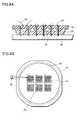
- FIG. 12is a diagram showing a transfer molding process.
- the semiconductor chip 1 fixed to a die pad of a lead frame 2 by die bonding or wire bondingis mounted inside a cavity 4 , formed of an upper and a lower die 3 A and 3 B, and an epoxy resin is injected into the cavity 4 to seal the semiconductor chip 1 .
- the lead frame 2is cut to complete the fabrication of a separate semiconductor device (e.g., Japanese Patent Publication No. H05-129473).
- multiple cavities 4 a to 4 fa resin source 5 for injecting a resin, a runner 6 , and gates 7 for injecting the resin into the cavities 4 a to 4 f via the runner 6 , are formed in the surface of the die 3 B.
- a resin source 5 for injecting a resinfor injecting a resin
- a runner 6for injecting the resin into the cavities 4 a to 4 f via the runner 6
- the cavities 4equivalent to, for example, twenty lead frames are formed in the inner surfaces of the die 3 .
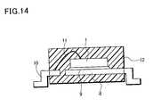
- FIG. 14is a diagram showing a semiconductor device obtained by transfer molding.
- the semiconductor chip 1 whereon elements, such as transistors, are formedis securely attached to an island 8 of the lead frame by a brazing material 9 , such as solder; the electrode pad of the semiconductor chip 1 is connected to a lead terminal 10 by a wire 11 ; the periphery of the semiconductor chip 1 is covered with a resin 12 that conforms to the shapes of the cavities 4 ; and the distal end of the lead terminal 10 is extended outside the resin 12 .
- the lead terminal 10 for an external connectionis exposed, outside the resin 12 , the distance up to the tip end of the lead terminal 10 must be considered as being part of the mounting area, and thus, the mounting area is much larger than the external dimensions of the resin 12 .
- a method for manufacturing a semiconductor devicecomprises the steps of:
- a method for manufacturing a semiconductor devicecomprises the steps of:
- FIG. 1is a perspective view for explaining a manufacturing method of the invention
- FIG. 2Ais a plan view for explaining the manufacturing method of the invention and FIG. 2B is a cross-sectional view for explaining the manufacturing method of the invention;
- FIG. 3is a plan view for explaining the manufacturing method of the invention.
- FIG. 4is a cross-sectional view for explaining the manufacturing method of the invention.
- FIG. 5Ais a cross-sectional view for explaining the manufacturing method of the invention and FIG. 5B is a cross-sectional view for explaining the manufacturing method of the invention;
- FIG. 6Ais a cross-sectional view for explaining the manufacturing method of the invention and FIG. 6B is a plan view for explaining the manufacturing method of the invention;
- FIG. 7Ais a cross-sectional view for explaining the manufacturing method of the invention and FIG. 7B is a plan view for explaining the manufacturing method of the invention;
- FIG. 8Ais a cross-sectional view for explaining the manufacturing method of the invention and FIG. 8B is a plan view for explaining the manufacturing method of the invention;
- FIG. 9Ais a cross-sectional view for explaining the manufacturing method of the invention.
- FIG. 9Bis a plan view for explaining the manufacturing method of the invention;
- FIG. 10Ais a plan view for explaining the manufacturing method of the invention
- FIG. 10Bis a cross-sectional view for explaining the manufacturing method of the invention
- FIG. 10Cis a cross-sectional view for explaining the manufacturing method of the invention
- FIG. 11Ais a perspective view for explaining the manufacturing method of the invention
- FIG. 11Bis a perspective view for explaining the manufacturing method of the invention
- FIG. 12is a cross-sectional view for explaining a conventional example
- FIG. 13is a plan view for explaining the conventional example.
- FIG. 14is a cross-sectional view for explaining the conventional example.
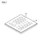
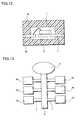
- a first step for this inventionis the preparation of a substrate having multiple mounting portions, as is shown in FIGS. 1 to 3 .
- a large substrate 21is prepared whereon positions are laid out for multiple mounting portions 20 for corresponding semiconductor devices, so as to provide, for example, a 100-mounting portion 20 arrangement of 10 rows and 10 columns.
- the substrate 21is a single or a multilayered glass epoxy or ceramic substrate having a total 200 to 350 [ ⁇ m] thickness that will provide adequate mechanical strength during the manufacturing process.
- each mounting portion 20 on the substrate 21On the obverse surface of each mounting portion 20 on the substrate 21 , a metal paste, such as tungsten, is printed on the obverse surface of each mounting portion 20 and a conductive pattern is formed by means of electrolytic-plating with gold. In addition, as an external connection electrode, an electrode pattern is formed on the reverse surface of the substrate 21 .
- a metal pastesuch as tungsten
- FIG. 2Ais a plan view of a conductive pattern formed on the surface of the substrate 21
- FIG. 2Bis a cross-sectional view of the substrate 21 .
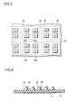
- the mounting portions 20 enclosed with broken linesare shaped like rectangles having, for example, long sides of 1.0 mm and short sides of 0.8 mm, and are arranged vertically and horizontally at intervals of 20 to 25 [ ⁇ m]. These intervals are used as dicing lines 24 for the following step.
- island portions 25 and lead portions 26are formed in each mounting portion 20 , and have the same shape in all mounting portions 20 .
- the island portions 25are where the semiconductor chips are mounted, and the lead portions 26 are the portions that are connected by wires to the electrode pads on the semiconductor chips.
- Two first connecting portions 27are extended from each island portion 25 to the lead portions 26 of adjacent mounting portion 20 with a continued pattern, and passing over dicing lines 24 on the way.
- the line width of the first connecting portions 27is narrower than the island portion 25 , e.g., 0.1 [mm].
- second connecting portions 28which also pass over dicing lines 24 but in a direction that is perpendicular to that of the first connecting portions 27 , are extended from lead portions 26 to the lead portions 26 of adjacent mounting portions 20 or to a common connecting portion 29 that encloses the entire group of mounting portions 20 . Since the first and the second connecting portions 27 and 28 are extended as they are, the island portions 25 and the lead portions 26 of all the mounting portions 20 are connected electrically. This arrangement is used because of the common electrodes that are prepared to perform electrolytic plating with gold or the like.
- a through hole 30is formed in each mounting portion 20 on the insulating substrate 21 and is filled with a conductive material, such as tungsten. And for each through hole 30 , a corresponding external electrode 31 is formed on the reverse surface.
- FIG. 3is a plan view of the pattern of external electrodes 31 a to 31 d , viewed from the reverse surface of the substrate 21 .
- the external electrodes 31 a , 31 b , 31 c and 31 dare provided 0.05 to 0.1 [mm] away from the ends of the mounting portions 20 .
- an individual patternis provided for the external electrodes 31 , they are all connected to the common connecting portion 29 via the through holes 30 .
- a gold-plated layercan be formed on all the conductive patterns by an electrolytic plating method for which the conductive pattern on the opposite side is employed as an electrode.
- only the first and second connecting portions 27 and 28which have narrow line widths, pass across the dicing lines 24 .
- a second step of the inventionis to fix a semiconductor chip to each of the mounting portions 20 by wire bonding, as is shown in FIG. 4.
- a semiconductor chip 33is attached by die bonding and wire bonding to each mounting portion 20 of the substrate 21 on which a gold-plated layer is formed.
- a semiconductor 33is fixed to the surface of an island portion 25 using an adhesive, such as a Ag paste, and the electrode pad of the semiconductor chip 33 is connected to lead portions by wires 34 .
- active devicesare formed that have three terminals, a bipolar transistor and a power MOSFET. When the bipolar devices are mounted, the external electrodes 31 a and 31 b , which are connected to the island portions 25 , act as collector terminals, and the external electrodes 31 c and 31 d , which are connected to the lead portions 26 act as base-emitter electrodes.
- a third step of the inventionis to cover the substrate 21 with a resin and to cover, with a common resin layer, the individual semiconductor chips bonded to the mounting portions, as is shown in FIGS. 5A and 5B.
- a predetermined amount of epoxy resin liquidis dropped (potting) from a dispenser (not shown) that is conveyed above the substrate 21 , and all the semiconductor chips 33 are covered with a common resin layer 35 .
- a dispensernot shown
- CV576ANMoshita Electric Works, Ltd.
- the dropped resin liquidis comparatively viscous and has a high surface tension, a curved resin surface is formed.
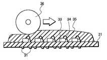
- the deposited resin layer 35is set by employing a thermal process (curing process) for several hours at a temperature of 100 to 200° C., and the surface of the resin layer 35 is then flattened by grinding the curved surface.
- a dicing machineis employed for the grinding, and a dicing blade 36 is used to grind the surface of the resin layer 35 and provide a surface that is aligned, at a constant height, with the substrate 21 .
- the height of the resin layer 35is reduced until it has a thickness of from 0.3 to 1.0 [mm], and the resulting flat surface extends from end to end of the resin layer 35 , so that even when the outermost semiconductor chips 33 are separated to obtain individual semiconductor devices, resin packages having a standard external size can be formed.
- dicing blades 36 of various thicknessesare prepared, and when the grinding is repeated multiple times using a comparatively thick dicing blade 36 , an overall flat structure is formed.
- the surface of the resin layer 35may also be flattened by pressing a flat formation member against the surface of the deposited resin layer 35 before it has fully hardened.
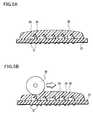
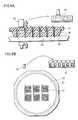
- a fourth step of the inventionis the gluing of a adhesive sheet 50 to the resin layer 35 covering the substrate 21 , as is shown in FIGS. 6A and 6B.
- the substrate 21is inverted, and the adhesive sheet (e.g., a UV sheet, the brand name of a Lintec Corporation product) is glued to the surface of the resin layer 35 . Since as a result of the processing performed at the previous step the surface of the resin layer 35 is flat and is horizontal to the surface of the substrate 21 , there is no tilting of the substrate 21 , even when the adhesive sheet 50 is glued to the surface of the resin layer 35 , and horizontal and vertical accuracy is maintained.
- the adhesive sheete.g., a UV sheet, the brand name of a Lintec Corporation product
- the circumferential edge of the adhesive sheet 50is glued to a ring-shaped stainless steel metal frame 51 , and in its center, six substrates 21 are glued at regular intervals.
- a fifth step of the inventionis the dicing of the substrate 21 and the resin layer 35 , performed from the reverse side of the substrate 21 , to cut out the mounting portions 20 and to thus obtain separate semiconductor devices.
- the substrate 21 and the resin layer 35 around each mounting portion 20are cut, and separate semiconductor devices are obtained.
- the resin layer 35 and the substrate 21are cut at the same time along the dicing lines 24 by the dicing blade 36 of the dicing machine, and separate semiconductor devices are obtained that correspond to the individual mounting portions 20 .
- the cutting depth during the dicing processis such that the dicing blade 36 reaches and penetrates the surface of the adhesive sheet 50 .
- an alignment marke.g., a through hole formed at the perimeter of the substrate 21 or in a portion of the gold-plated layer
- this alignment markis used as a position reference while the dicing is being performed.
- the patternis so designed that the dicing blade 36 does not contact the conductive patterns 31 a , 31 b , 31 c and 31 d and the island portions 25 . This is because, since the separation of the gold-plated layer is comparatively inferior, the occurrence of burrs at the gold-plated layer is prevented to the extent possible. Therefore, the dicing blade 36 contacts the gold-plated layer only at the first and the second connecting portions 27 and 28 , which are used as electrical connections.
- a sixth step of the inventionis the measurement of the characteristics of the semiconductor devices integrally supported by the adhesive sheet 50 .
- a probe 52is brought into contact with the external electrodes 31 a to 31 d that are exposed on the reverse surfaces of the substrates 21 of the semiconductor devices that are integrally supported by the adhesive sheet 50 . And then the characteristic parameters of the individual semiconductor devices are measured to determine their qualities, and magnetic ink is used to mark defective devices.
- the metal frame 51need only be moved vertically and horizontally a pitch equivalent to the size of one semiconductor device for an extremely large number of semiconductor devices to be easily measured. That is, a determination of the obverse and reverse sides of semiconductor devices, and a determination of the types, for example, of emitters, bases and collectors provided for external electrodes are not required.
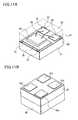
- a seventh step of the inventionis, as is shown in FIGS. 9A and 9B, the direct storage in a carrier tape 41 of the semiconductor devices integrally supported by the adhesive sheet 50 .
- the metal frame 51need only be moved a pitch equivalent to the size of one semiconductor device to enable the extremely easy storage of a large number of semiconductor devices in the carrier tape 41 .
- FIG. 10Ais a plan view of the carrier tape 41 used for this step
- FIG. 10Bis a cross-sectional view taken along line AA
- FIG. 10Cis a cross-sectional view taken along line BB.
- the tape 41is a belt-shaped member having a film thickness of from 0.5 to 1.0 [mm], a width of from 6 to 15 [mm] and a length of several tens of meters, and is made of paper, shaped like corrugated cardboard.
- Through holes 42are formed in the tape 41 at predetermined intervals, and feed holes 43 are also formed at a predetermined pitch to feed the tape 41 .
- a dieis used to punch the through holes 42 and the feed holes 43 in the tape, and the film thickness of the tape 41 and the size of the through holes 42 are determined in accordance with the sizes of the electronic parts 40 that are to be packed.
- a first tape 44 of transparent filmis adhered to the reverse surface of the tape 41 to close the bottoms of the through holes 42 .
- a second tape 45 of transparent filmis adhered to the obverse surface of the tape 41 to close the tops of the through holes 42 .
- the second tape 45is attached to the tape 41 at adhesive portions 46 near the side edges, while the first tape 44 is attached at corresponding locations along the reverse surface of the tape 41 .
- This adhesive processis performed by thermally bonding the films from above using a member that has heaters positioned at locations corresponding to the adhesion potions 46 . After undergoing this adhesive process, the tapes can be peeled apart simply by pulling on the films.
- FIGS. 11A and 11Bare perspective views of one semiconductor device package obtained as a result of the above described processing.
- the four side surfaces of the packageare cut surfaces formed when the resin layer 35 and the substrate 21 were cut along the dicing lines 24 , the top surface of the package is the flattened surface of the resin layer 35 , and the bottom of the package is the reverse surface of the insulating substrate 21 .
- This semiconductor devicehas a depth of 1.0 [mm], a width of 0.6 [mm] and a height of 0.5 [mm].
- the substrate 21is covered with the resin layer 35 which has a thickness of about 0.5 [mm].
- the island portion 25 and the lead portion 26are retracted from the end surface of the package, and along the package side surface, only the cut portions of the first and the second connecting portions 27 and 28 are exposed.
- the external electrodes 31 a to 31 dwhich are about 0.2 ⁇ 0.3 [mm], are arranged at the four corners of the substrate 21 in a pattern horizontally (vertically) symmetrical to the center line of the external package shape. Since this symmetrical arrangement makes the determination of the polarity of the electrode difficult, it is preferable that a polarity mark be provided by forming an indentation in the obverse surface of the resin layer, or by a printed mark.
- semiconductor devicesare produced by collectively packaging multiple devices, a reduction can be realized in the resin material that is wasted, compared with when such devices are individually packaged, and expenditures for material can be reduced. Also, since a lead frame is not required, a package can be provided that, when compared with the conventional transfer molding method, has a considerably smaller external size. And in addition, since external connection terminals are formed on the reverse surface of the substrate 21 so that they do not protrude and extend outward from the package, a considerably reduced mounting area is required for the device.
- the adhesive sheet 50is glued not to the substrate 21 but to the resin layer 35 . If, for example, the adhesive sheet 50 were glued to the substrate 21 , when the devices were removed from the adhesive sheet 50 , the viscous agent from the adhesive sheet 50 would be attached to the surfaces of the external electrodes 31 a to 31 d . And if the device were introduced to the automatic mounting apparatus while the viscous agent was attached, soldering of the electrodes 31 a to 31 d would be deteriorated. Further, a problem due to the attachment of dust to the surfaces of the electrodes 31 a to 31 d should also be taken into account. However, since the adhesive sheet 50 is attached to the resin layer 35 in this invention, these problems are resolved.
- the inventionfirst, multiple substrates are covered with a resin layer, and are adhered to an adhesive sheet, the circumferential edge of which is glued to a metal frame, and in this state, the dicing process and the measurement process can be performed for the substrate. Therefore, a semiconductor device manufacturing method having an extremely high productivity can be implemented, regardless of whether the package structure is tiny.
- the semiconductor devicescan be stored in the carrier tape, while the multiple substrates are adhered to the adhesive sheet, the circumferential edge of which is attached to the metal frame. Therefore, the semiconductor device can be handled on the substrate base, regardless of the size of the tiny package, and a semiconductor device manufacturing method can be provided for which productivity is extremely high.
Landscapes
- Engineering & Computer Science (AREA)
- Microelectronics & Electronic Packaging (AREA)
- Computer Hardware Design (AREA)
- Power Engineering (AREA)
- Physics & Mathematics (AREA)
- Condensed Matter Physics & Semiconductors (AREA)
- General Physics & Mathematics (AREA)
- Manufacturing & Machinery (AREA)
- Encapsulation Of And Coatings For Semiconductor Or Solid State Devices (AREA)
- Dicing (AREA)
Abstract
Description
- The present invention relates to a method for manufacturing a semiconductor device, and relates in particular to a method for manufacturing a semiconductor device whereby a smaller mounting area can be provided by reducing the external size of a package without using lead forming, and a considerable reduction in manufacturing costs can be realized.[0001]
- In a process for the manufacture of semiconductor devices, multiple semiconductor chips, produced from a single wafer by dicing, are securely mounted in a lead frame, after which transfer molding, using a die and resin injection, is used to seal them. The thus sealed semiconductor chips are then separated to provide multiple individual semiconductor devices. For this process, either a strip-shaped or a hoop-shaped lead frame is employed, but regardless of which type of lead frame is used, only a single sealing procedure is required to simultaneously seal a plurality of semiconductor devices.[0002]
- FIG. 12 is a diagram showing a transfer molding process. During this process, the[0003]
semiconductor chip 1 fixed to a die pad of alead frame 2 by die bonding or wire bonding is mounted inside acavity 4, formed of an upper and alower die cavity 4 to seal thesemiconductor chip 1. Once the process has been completed, thelead frame 2 is cut to complete the fabrication of a separate semiconductor device (e.g., Japanese Patent Publication No. H05-129473). - For this process, as is shown in FIG. 13,[0004]
multiple cavities 4ato4f, aresin source 5 for injecting a resin, arunner 6, and gates7 for injecting the resin into thecavities 4ato4fvia therunner 6, are formed in the surface of thedie 3B. For example, if tensemiconductor chips 1 are mounted on a single lead frame, tencavities 4, ten gates7 and onerunner 6 are formed for one lead frame. And thecavities 4 equivalent to, for example, twenty lead frames are formed in the inner surfaces of thedie 3. - FIG. 14 is a diagram showing a semiconductor device obtained by transfer molding. The[0005]
semiconductor chip 1 whereon elements, such as transistors, are formed is securely attached to anisland 8 of the lead frame by abrazing material 9, such as solder; the electrode pad of thesemiconductor chip 1 is connected to alead terminal 10 by awire 11; the periphery of thesemiconductor chip 1 is covered with aresin 12 that conforms to the shapes of thecavities 4; and the distal end of thelead terminal 10 is extended outside theresin 12. - Since, in a conventional package, the[0006]
lead terminal 10 for an external connection is exposed, outside theresin 12, the distance up to the tip end of thelead terminal 10 must be considered as being part of the mounting area, and thus, the mounting area is much larger than the external dimensions of theresin 12. - Further, since according to the conventional transfer molding technique the resin is hardened under pressure, even the resin in the[0007]
runner 6 and the gates7 is hardened, and the residual resin therein must be disposed of. Thus, according to the method using the above lead frame whereby the gates7 are provided for the individual semiconductor devices that are to be manufactured, efficiency in the use of the resin is low, and relative to the amount of resin employed, only a small number of semiconductor devices can be manufactured. - Further, since, after a transfer molding process a lead frame is separated into tiny packages comprising individual semiconductor devices, it is extremely difficult to handle the obtained semiconductor devices when they must be measured or stored in tape because it is difficult to determine which are their obverse and which are their reverse sides, and because of how the lead terminals are positioned. As a result, work efficiency is adversely affected and greatly deteriorated.[0008]
- To achieve the shortcomings, according to the invention, a method for manufacturing a semiconductor device comprises the steps of:[0009]
- bonding one semiconductor chip to each of multiple mounting portions of a substrate;[0010]
- covering the semiconductor chips bonded to the mounting portions with a common resin layer;[0011]
- bringing the substrate into contact with the resin layer and gluing the substrate to a adhesive sheet;[0012]
- performing dicing and measurement for the semiconductor chips that are glued to the adhesive sheet. Thus, the semiconductor chips that are integrally supported by the adhesive sheet can be measured, without the having to be separated into individual semiconductor devices.[0013]
- Further, according to the invention, a method for manufacturing a semiconductor device comprises the steps of:[0014]
- bonding a semiconductor chip to each of multiple mounting portions of a substrate;[0015]
- covering the semiconductor chips bonded to the mounting portions with a common resin layer;[0016]
- bringing the substrate into contact with the resin layer and gluing the substrate to an adhesive sheet;[0017]
- dicing and measuring the semiconductor chips while the substrate is glued to the adhesive sheet; and[0018]
- storing directly in a carrier tape semiconductor devices glued to the adhesive sheet. Thus, the semiconductor chips can be processed while integrally supported by the adhesive sheet, and need not be separated into individual semiconductor devices until they are stored in a carrier tape.[0019]
- FIG. 1 is a perspective view for explaining a manufacturing method of the invention;[0020]
- FIG. 2A is a plan view for explaining the manufacturing method of the invention and FIG. 2B is a cross-sectional view for explaining the manufacturing method of the invention;[0021]
- FIG. 3 is a plan view for explaining the manufacturing method of the invention;[0022]
- FIG. 4 is a cross-sectional view for explaining the manufacturing method of the invention;[0023]
- FIG. 5A is a cross-sectional view for explaining the manufacturing method of the invention and FIG. 5B is a cross-sectional view for explaining the manufacturing method of the invention;[0024]
- FIG. 6A is a cross-sectional view for explaining the manufacturing method of the invention and FIG. 6B is a plan view for explaining the manufacturing method of the invention;[0025]
- FIG. 7A is a cross-sectional view for explaining the manufacturing method of the invention and FIG. 7B is a plan view for explaining the manufacturing method of the invention;[0026]
- FIG. 8A is a cross-sectional view for explaining the manufacturing method of the invention and FIG. 8B is a plan view for explaining the manufacturing method of the invention;[0027]
- FIG. 9A is a cross-sectional view for explaining the manufacturing method of the invention; and FIG. 9B is a plan view for explaining the manufacturing method of the invention;[0028]
- FIG. 10A is a plan view for explaining the manufacturing method of the invention, FIG. 10B is a cross-sectional view for explaining the manufacturing method of the invention; and FIG. 10C is a cross-sectional view for explaining the manufacturing method of the invention;[0029]
- FIG. 11A is a perspective view for explaining the manufacturing method of the invention, and FIG. 11B is a perspective view for explaining the manufacturing method of the invention;[0030]
- FIG. 12 is a cross-sectional view for explaining a conventional example;[0031]
- FIG. 13 is a plan view for explaining the conventional example; and[0032]
- FIG. 14 is a cross-sectional view for explaining the conventional example.[0033]
- The preferred embodiment of the invention will now be described in detail.[0034]
- A first step for this invention is the preparation of a substrate having multiple mounting portions, as is shown in FIGS.[0035]1 to3.
- First, as is shown in FIG. 1, a[0036]
large substrate 21 is prepared whereon positions are laid out for multiple mountingportions 20 for corresponding semiconductor devices, so as to provide, for example, a 100-mountingportion 20 arrangement of 10 rows and 10 columns. Thesubstrate 21 is a single or a multilayered glass epoxy or ceramic substrate having a total 200 to 350 [μm] thickness that will provide adequate mechanical strength during the manufacturing process. - On the obverse surface of each mounting[0037]
portion 20 on thesubstrate 21, a metal paste, such as tungsten, is printed on the obverse surface of each mountingportion 20 and a conductive pattern is formed by means of electrolytic-plating with gold. In addition, as an external connection electrode, an electrode pattern is formed on the reverse surface of thesubstrate 21. - FIG. 2A is a plan view of a conductive pattern formed on the surface of the[0038]
substrate 21, and FIG. 2B is a cross-sectional view of thesubstrate 21. - The mounting[0039]
portions 20 enclosed with broken lines are shaped like rectangles having, for example, long sides of 1.0 mm and short sides of 0.8 mm, and are arranged vertically and horizontally at intervals of 20 to 25 [μm]. These intervals are used as dicinglines 24 for the following step. As the conductive patterns,island portions 25 and leadportions 26 are formed in each mountingportion 20, and have the same shape in all mountingportions 20. Theisland portions 25 are where the semiconductor chips are mounted, and thelead portions 26 are the portions that are connected by wires to the electrode pads on the semiconductor chips. Two first connectingportions 27 are extended from eachisland portion 25 to thelead portions 26 of adjacent mountingportion 20 with a continued pattern, and passing over dicinglines 24 on the way. The line width of the first connectingportions 27 is narrower than theisland portion 25, e.g., 0.1 [mm]. In addition, second connectingportions 28, which also pass over dicinglines 24 but in a direction that is perpendicular to that of the first connectingportions 27, are extended fromlead portions 26 to thelead portions 26 of adjacent mountingportions 20 or to a common connectingportion 29 that encloses the entire group of mountingportions 20. Since the first and the second connectingportions island portions 25 and thelead portions 26 of all the mountingportions 20 are connected electrically. This arrangement is used because of the common electrodes that are prepared to perform electrolytic plating with gold or the like. - In FIG. 2B, a through[0040]
hole 30 is formed in each mountingportion 20 on the insulatingsubstrate 21 and is filled with a conductive material, such as tungsten. And for each throughhole 30, a correspondingexternal electrode 31 is formed on the reverse surface. - FIG. 3 is a plan view of the pattern of[0041]
external electrodes 31ato31d, viewed from the reverse surface of thesubstrate 21. Theexternal electrodes portions 20. Although an individual pattern is provided for theexternal electrodes 31, they are all connected to the common connectingportion 29 via the through holes30. Thus, a gold-plated layer can be formed on all the conductive patterns by an electrolytic plating method for which the conductive pattern on the opposite side is employed as an electrode. Further, only the first and second connectingportions - A second step of the invention is to fix a semiconductor chip to each of the mounting[0042]
portions 20 by wire bonding, as is shown in FIG. 4. - A[0043]
semiconductor chip 33 is attached by die bonding and wire bonding to each mountingportion 20 of thesubstrate 21 on which a gold-plated layer is formed. Asemiconductor 33 is fixed to the surface of anisland portion 25 using an adhesive, such as a Ag paste, and the electrode pad of thesemiconductor chip 33 is connected to lead portions bywires 34. As the semiconductor chips33, active devices are formed that have three terminals, a bipolar transistor and a power MOSFET. When the bipolar devices are mounted, theexternal electrodes island portions 25, act as collector terminals, and theexternal electrodes lead portions 26 act as base-emitter electrodes. - A third step of the invention is to cover the[0044]
substrate 21 with a resin and to cover, with a common resin layer, the individual semiconductor chips bonded to the mounting portions, as is shown in FIGS. 5A and 5B. - As is shown in FIG. 5A, a predetermined amount of epoxy resin liquid is dropped (potting) from a dispenser (not shown) that is conveyed above the[0045]
substrate 21, and all the semiconductor chips33 are covered with acommon resin layer 35. When, for example, 100semiconductor chips 33 are mounted on onesubstrate 21, all 100semiconductor chips 33 are collectively covered. For this, CV576AN (Matsushita Electric Works, Ltd.) is employed as the liquid resin. And since the dropped resin liquid is comparatively viscous and has a high surface tension, a curved resin surface is formed. - Following this, as is shown in FIG. 5B, the deposited[0046]
resin layer 35 is set by employing a thermal process (curing process) for several hours at a temperature of 100 to 200° C., and the surface of theresin layer 35 is then flattened by grinding the curved surface. A dicing machine is employed for the grinding, and adicing blade 36 is used to grind the surface of theresin layer 35 and provide a surface that is aligned, at a constant height, with thesubstrate 21. At this step, the height of theresin layer 35 is reduced until it has a thickness of from 0.3 to 1.0 [mm], and the resulting flat surface extends from end to end of theresin layer 35, so that even when theoutermost semiconductor chips 33 are separated to obtain individual semiconductor devices, resin packages having a standard external size can be formed. For this process, dicingblades 36 of various thicknesses are prepared, and when the grinding is repeated multiple times using a comparativelythick dicing blade 36, an overall flat structure is formed. - The surface of the[0047]
resin layer 35 may also be flattened by pressing a flat formation member against the surface of the depositedresin layer 35 before it has fully hardened. - A fourth step of the invention is the gluing of a[0048]
adhesive sheet 50 to theresin layer 35 covering thesubstrate 21, as is shown in FIGS. 6A and 6B. - As is shown in FIG. 6A, the[0049]
substrate 21 is inverted, and the adhesive sheet (e.g., a UV sheet, the brand name of a Lintec Corporation product) is glued to the surface of theresin layer 35. Since as a result of the processing performed at the previous step the surface of theresin layer 35 is flat and is horizontal to the surface of thesubstrate 21, there is no tilting of thesubstrate 21, even when theadhesive sheet 50 is glued to the surface of theresin layer 35, and horizontal and vertical accuracy is maintained. - As is shown in FIG. 6B, the circumferential edge of the[0050]
adhesive sheet 50 is glued to a ring-shaped stainlesssteel metal frame 51, and in its center, sixsubstrates 21 are glued at regular intervals. - A fifth step of the invention, as is shown in FIGS. 7A and 7B, is the dicing of the[0051]
substrate 21 and theresin layer 35, performed from the reverse side of thesubstrate 21, to cut out the mountingportions 20 and to thus obtain separate semiconductor devices. - As is shown in FIG. 7A, the[0052]
substrate 21 and theresin layer 35 around each mountingportion 20 are cut, and separate semiconductor devices are obtained. Theresin layer 35 and thesubstrate 21 are cut at the same time along the dicinglines 24 by thedicing blade 36 of the dicing machine, and separate semiconductor devices are obtained that correspond to the individual mountingportions 20. The cutting depth during the dicing process is such that thedicing blade 36 reaches and penetrates the surface of theadhesive sheet 50. At this time, an alignment mark (e.g., a through hole formed at the perimeter of thesubstrate 21 or in a portion of the gold-plated layer) that can be observed from the reverse side of thesubstrate 21 can be automatically identified by the dicing machine, and this alignment mark is used as a position reference while the dicing is being performed. Further, the pattern is so designed that thedicing blade 36 does not contact theconductive patterns island portions 25. This is because, since the separation of the gold-plated layer is comparatively inferior, the occurrence of burrs at the gold-plated layer is prevented to the extent possible. Therefore, thedicing blade 36 contacts the gold-plated layer only at the first and the second connectingportions - As is shown in FIG. 7B,[0053]
multiple substrates 21 glued to theadhesive sheet 50, which around its circumference is glued to themetal frame 51, are separated by the dicing machine along thevertical dicing lines 24, which for eachsubstrate 21 are individually identified. Then, themetal frame 51 is rotated 90 degrees, and thesubstrates 21 are separated along the horizontal dicing lines24. The semiconductor devices obtained by the dicing continue to be supported on theadhesive sheet 50 by the viscous agent, and are not separated individually. - A sixth step of the invention, as is shown in FIGS. 8A and 8B, is the measurement of the characteristics of the semiconductor devices integrally supported by the[0054]
adhesive sheet 50. - As is shown in FIG. 8A, a[0055]
probe 52 is brought into contact with theexternal electrodes 31ato31dthat are exposed on the reverse surfaces of thesubstrates 21 of the semiconductor devices that are integrally supported by theadhesive sheet 50. And then the characteristic parameters of the individual semiconductor devices are measured to determine their qualities, and magnetic ink is used to mark defective devices. - As is shown in FIG. 8B, since[0056]
multiple substrates 21 are supported by themetal frame 51 and the individual semiconductor devices are maintained in the state obtained at the dicing step, themetal frame 51 need only be moved vertically and horizontally a pitch equivalent to the size of one semiconductor device for an extremely large number of semiconductor devices to be easily measured. That is, a determination of the obverse and reverse sides of semiconductor devices, and a determination of the types, for example, of emitters, bases and collectors provided for external electrodes are not required. - A seventh step of the invention is, as is shown in FIGS. 9A and 9B, the direct storage in a[0057]
carrier tape 41 of the semiconductor devices integrally supported by theadhesive sheet 50. - As is shown in FIG. 9A, after the measurements performed for the semiconductor devices integrally supported by the[0058]
adhesive sheet 50, only those devices for which excellent results were obtained are peeled from theadhesive sheet 50 by avacuum collet 53, and are deposited in storage holes in thecarrier tape 41. - As is shown in FIG. 9B, since[0059]
multiple substrates 21 are supported by themetal frame 51, and since individual semiconductor devices are maintained in the state obtained at the dicing step, themetal frame 51 need only be moved a pitch equivalent to the size of one semiconductor device to enable the extremely easy storage of a large number of semiconductor devices in thecarrier tape 41. - FIG. 10A is a plan view of the[0060]
carrier tape 41 used for this step, FIG. 10B is a cross-sectional view taken along line AA, and FIG. 10C is a cross-sectional view taken along line BB. Thetape 41 is a belt-shaped member having a film thickness of from 0.5 to 1.0 [mm], a width of from 6 to 15 [mm] and a length of several tens of meters, and is made of paper, shaped like corrugated cardboard. Throughholes 42 are formed in thetape 41 at predetermined intervals, and feedholes 43 are also formed at a predetermined pitch to feed thetape 41. A die is used to punch the throughholes 42 and the feed holes43 in the tape, and the film thickness of thetape 41 and the size of the throughholes 42 are determined in accordance with the sizes of theelectronic parts 40 that are to be packed. - A[0061]
first tape 44 of transparent film is adhered to the reverse surface of thetape 41 to close the bottoms of the through holes42. And similarly, asecond tape 45 of transparent film is adhered to the obverse surface of thetape 41 to close the tops of the through holes42. Thesecond tape 45 is attached to thetape 41 atadhesive portions 46 near the side edges, while thefirst tape 44 is attached at corresponding locations along the reverse surface of thetape 41. This adhesive process is performed by thermally bonding the films from above using a member that has heaters positioned at locations corresponding to theadhesion potions 46. After undergoing this adhesive process, the tapes can be peeled apart simply by pulling on the films. - Finally, FIGS. 11A and 11B are perspective views of one semiconductor device package obtained as a result of the above described processing. The four side surfaces of the package are cut surfaces formed when the[0062]
resin layer 35 and thesubstrate 21 were cut along the dicinglines 24, the top surface of the package is the flattened surface of theresin layer 35, and the bottom of the package is the reverse surface of the insulatingsubstrate 21. - This semiconductor device has a depth of 1.0 [mm], a width of 0.6 [mm] and a height of 0.5 [mm]. To seal the[0063]
semiconductor chip 33 which has a thickness of about 150 [μm], thesubstrate 21 is covered with theresin layer 35 which has a thickness of about 0.5 [mm]. Theisland portion 25 and thelead portion 26 are retracted from the end surface of the package, and along the package side surface, only the cut portions of the first and the second connectingportions - The[0064]
external electrodes 31ato31dwhich are about 0.2×0.3 [mm], are arranged at the four corners of thesubstrate 21 in a pattern horizontally (vertically) symmetrical to the center line of the external package shape. Since this symmetrical arrangement makes the determination of the polarity of the electrode difficult, it is preferable that a polarity mark be provided by forming an indentation in the obverse surface of the resin layer, or by a printed mark. - Since with this manufacturing method semiconductor devices are produced by collectively packaging multiple devices, a reduction can be realized in the resin material that is wasted, compared with when such devices are individually packaged, and expenditures for material can be reduced. Also, since a lead frame is not required, a package can be provided that, when compared with the conventional transfer molding method, has a considerably smaller external size. And in addition, since external connection terminals are formed on the reverse surface of the[0065]
substrate 21 so that they do not protrude and extend outward from the package, a considerably reduced mounting area is required for the device. - Further, according to the manufacturing method of the invention, for the dicing, the[0066]
adhesive sheet 50 is glued not to thesubstrate 21 but to theresin layer 35. If, for example, theadhesive sheet 50 were glued to thesubstrate 21, when the devices were removed from theadhesive sheet 50, the viscous agent from theadhesive sheet 50 would be attached to the surfaces of theexternal electrodes 31ato31d. And if the device were introduced to the automatic mounting apparatus while the viscous agent was attached, soldering of theelectrodes 31ato31dwould be deteriorated. Further, a problem due to the attachment of dust to the surfaces of theelectrodes 31ato31dshould also be taken into account. However, since theadhesive sheet 50 is attached to theresin layer 35 in this invention, these problems are resolved. - Since the surface of the[0067]
resin layer 35 is flattened and is horizontal to thesubstrate 21 before theadhesive sheet 50 is adhered to theresin layer 35, the same vertical and horizontal accuracy can be maintained as is obtained when theadhesive sheet 50 is adhered to thesubstrate 21. - In this embodiment, four external electrodes are formed while the three-terminal devices are sealed. However, this embodiment can also be applied to a case wherein two semiconductor chips are sealed or an integrated circuit is sealed.[0068]
- According to the invention, first, multiple substrates are covered with a resin layer, and are adhered to an adhesive sheet, the circumferential edge of which is glued to a metal frame, and in this state, the dicing process and the measurement process can be performed for the substrate. Therefore, a semiconductor device manufacturing method having an extremely high productivity can be implemented, regardless of whether the package structure is tiny.[0069]
- Second, the semiconductor devices can be stored in the carrier tape, while the multiple substrates are adhered to the adhesive sheet, the circumferential edge of which is attached to the metal frame. Therefore, the semiconductor device can be handled on the substrate base, regardless of the size of the tiny package, and a semiconductor device manufacturing method can be provided for which productivity is extremely high.[0070]
- Third, according to the manufacturing method, since resin is used for the collective packaging of multiple semiconductor devices, compared with when the devices are individually packaged, there is less resin material waste, and a savings in the expenditures for materials can be realized. Further, since a lead frame is not required, the external size of a package can be considerably reduced, compared with when the conventional transfer molding method is applied. In addition, since the external connection terminals are formed on the reverse surface of the[0071]
substrate 21, and are not exposed and extend outward from the package, a much smaller mounting area is required for the device. Thus, a product can be provided for which the environment is taken into account. - Fourth, according to the invention, since a lead frame is not employed, a transfer molding apparatus is not required, and accordingly, a separate die is not required for each package shape used by this transfer molding apparatus. And as a result, a resource saving manufacturing line can be provided.[0072]
- Fifth, since the adhesive sheet fixed to the metal frame is only required when the dicing process, the measurement process and the taping process are performed, as a tool, only the metal frame is required for this manufacturing process, so that the size of a manufacturing line can be reduced, while the dicing to taping processes can be continuously performed by employing only one manufacturing apparatus.[0073]
Claims (16)
Applications Claiming Priority (2)
| Application Number | Priority Date | Filing Date | Title |
|---|---|---|---|
| JPP.2000-206305 | 2000-07-07 | ||
| JP2000206305AJP2002026182A (en) | 2000-07-07 | 2000-07-07 | Method for manufacturing semiconductor device |
Publications (2)
| Publication Number | Publication Date |
|---|---|
| US20020004250A1true US20020004250A1 (en) | 2002-01-10 |
| US6737285B2 US6737285B2 (en) | 2004-05-18 |
Family
ID=18703252
Family Applications (1)
| Application Number | Title | Priority Date | Filing Date |
|---|---|---|---|
| US09/900,093Expired - LifetimeUS6737285B2 (en) | 2000-07-07 | 2001-07-06 | Semiconductor device manufacturing method |
Country Status (5)
| Country | Link |
|---|---|
| US (1) | US6737285B2 (en) |
| JP (1) | JP2002026182A (en) |
| KR (1) | KR20020005461A (en) |
| CN (1) | CN1183585C (en) |
| TW (1) | TW492171B (en) |
Cited By (13)
| Publication number | Priority date | Publication date | Assignee | Title |
|---|---|---|---|---|
| US20030025118A1 (en)* | 2001-07-27 | 2003-02-06 | Shunpei Yamazaki | Light emitting device, semiconductor device, and method of fabricating the devices |
| US20030047280A1 (en)* | 2001-08-22 | 2003-03-13 | Toru Takayama | Peeling method and method of manufacturing semiconductor device |
| US20030082889A1 (en)* | 2001-10-30 | 2003-05-01 | Junya Maruyama | Semiconductor device and method of manufacturing the same |
| US20030162312A1 (en)* | 2001-11-30 | 2003-08-28 | Semiconductor Energy Laboratory Co., Ltd. | Vehicle, display device and manufacturing method for a semiconductor device |
| US20040232413A1 (en)* | 2002-10-30 | 2004-11-25 | Semiconductor Energy Laboratory Co., Ltd. | Semiconductor device and manufacturing method thereof |
| US20070085138A1 (en)* | 2001-08-01 | 2007-04-19 | Shunpei Yamazaki | Semiconductor device and manufacturing method thereof |
| US20070171619A1 (en)* | 2003-12-26 | 2007-07-26 | Toray Engineering Co., Ltd. | Electronic circuit board intermediate member, manufacturing method therefor, manufacturing equipment therefor, method for rmanufacturing noncontact id card and the like, and equipment therefor |
| US8415208B2 (en) | 2001-07-16 | 2013-04-09 | Semiconductor Energy Laboratory Co., Ltd. | Semiconductor device and peeling off method and method of manufacturing semiconductor device |
| EP2320718A4 (en)* | 2008-08-19 | 2017-08-02 | Murata Manufacturing Co. Ltd. | Circuit module and method for manufacturing same |
| US9947568B2 (en) | 2013-02-20 | 2018-04-17 | Semiconductor Energy Laboratory Co., Ltd. | Peeling method, semiconductor device, and peeling apparatus |
| US10189048B2 (en) | 2013-12-12 | 2019-01-29 | Semiconductor Energy Laboratory Co., Ltd. | Peeling method and peeling apparatus |
| US10944046B2 (en)* | 2017-09-04 | 2021-03-09 | Rohm Co., Ltd. | Semiconductor device |
| US11729915B1 (en)* | 2022-03-22 | 2023-08-15 | Tactotek Oy | Method for manufacturing a number of electrical nodes, electrical node module, electrical node, and multilayer structure |
Families Citing this family (10)
| Publication number | Priority date | Publication date | Assignee | Title |
|---|---|---|---|---|
| JP2002190457A (en)* | 2000-12-20 | 2002-07-05 | Fdk Corp | Method of manufacturing and handling element with directionality |
| TW554398B (en)* | 2001-08-10 | 2003-09-21 | Semiconductor Energy Lab | Method of peeling off and method of manufacturing semiconductor device |
| JP3831287B2 (en)* | 2002-04-08 | 2006-10-11 | 株式会社日立製作所 | Manufacturing method of semiconductor device |
| JP2007096196A (en)* | 2005-09-30 | 2007-04-12 | Renesas Technology Corp | Manufacturing method for semiconductor device |
| CN101101882A (en)* | 2006-07-05 | 2008-01-09 | 阎跃军 | Substrate resin packaging method |
| CN103000768A (en)* | 2011-09-09 | 2013-03-27 | 展晶科技(深圳)有限公司 | Method for manufacturing light emitting diode packaging structure |
| US9847445B2 (en)* | 2012-04-05 | 2017-12-19 | Koninklijke Philips N.V. | LED thin-film device partial singulation prior to substrate thinning or removal |
| JP2014017357A (en)* | 2012-07-09 | 2014-01-30 | Nitto Denko Corp | Adhesive tape, pasting method of adhesive tape and pasting device of adhesive tape |
| SG11201804481WA (en)* | 2016-02-24 | 2018-06-28 | Lintec Corp | Adhesive sheet and usage method therefor |
| WO2020244744A1 (en) | 2019-06-04 | 2020-12-10 | Grumago - Gruber Materials And Goods E.K. | Collapsible container |
Citations (3)
| Publication number | Priority date | Publication date | Assignee | Title |
|---|---|---|---|---|
| US5814894A (en)* | 1995-04-07 | 1998-09-29 | Nitto Denko Corporation | Semiconductor device, production method thereof, and tape carrier for semiconductor device used for producing the semiconductor device |
| US6113728A (en)* | 1989-03-09 | 2000-09-05 | Hitachi Chemical Company, Ltd. | Process for connecting circuits and adhesive film used therefor |
| US6528330B2 (en)* | 2000-08-03 | 2003-03-04 | Sanyo Electric Co., Ltd. | Semiconductor device manufacturing method |
Family Cites Families (8)
| Publication number | Priority date | Publication date | Assignee | Title |
|---|---|---|---|---|
| US5541525A (en)* | 1991-06-04 | 1996-07-30 | Micron Technology, Inc. | Carrier for testing an unpackaged semiconductor die |
| JPH05129473A (en) | 1991-11-06 | 1993-05-25 | Sony Corp | Resin-sealed surface-mounting semiconductor device |
| US6048750A (en)* | 1997-11-24 | 2000-04-11 | Micron Technology, Inc. | Method for aligning and connecting semiconductor components to substrates |
| JP3819574B2 (en)* | 1997-12-25 | 2006-09-13 | 三洋電機株式会社 | Manufacturing method of semiconductor device |
| JP2000114204A (en)* | 1998-10-01 | 2000-04-21 | Mitsubishi Electric Corp | Wafer sheet, method of manufacturing semiconductor device using the same, and semiconductor manufacturing apparatus |
| JP3877454B2 (en)* | 1998-11-27 | 2007-02-07 | 三洋電機株式会社 | Manufacturing method of semiconductor device |
| JP4803855B2 (en)* | 1999-02-09 | 2011-10-26 | 三洋電機株式会社 | Manufacturing method of semiconductor device |
| JP3738176B2 (en)* | 2000-08-03 | 2006-01-25 | 三洋電機株式会社 | Manufacturing method of semiconductor device |
- 2000
- 2000-07-07JPJP2000206305Apatent/JP2002026182A/enactivePending
- 2001
- 2001-04-18TWTW090109244Apatent/TW492171B/ennot_activeIP Right Cessation
- 2001-07-06USUS09/900,093patent/US6737285B2/ennot_activeExpired - Lifetime
- 2001-07-06KRKR1020010040228Apatent/KR20020005461A/ennot_activeCeased
- 2001-07-09CNCNB011228296Apatent/CN1183585C/ennot_activeExpired - Lifetime
Patent Citations (3)
| Publication number | Priority date | Publication date | Assignee | Title |
|---|---|---|---|---|
| US6113728A (en)* | 1989-03-09 | 2000-09-05 | Hitachi Chemical Company, Ltd. | Process for connecting circuits and adhesive film used therefor |
| US5814894A (en)* | 1995-04-07 | 1998-09-29 | Nitto Denko Corporation | Semiconductor device, production method thereof, and tape carrier for semiconductor device used for producing the semiconductor device |
| US6528330B2 (en)* | 2000-08-03 | 2003-03-04 | Sanyo Electric Co., Ltd. | Semiconductor device manufacturing method |
Cited By (48)
| Publication number | Priority date | Publication date | Assignee | Title |
|---|---|---|---|---|
| US8415208B2 (en) | 2001-07-16 | 2013-04-09 | Semiconductor Energy Laboratory Co., Ltd. | Semiconductor device and peeling off method and method of manufacturing semiconductor device |
| US20030025118A1 (en)* | 2001-07-27 | 2003-02-06 | Shunpei Yamazaki | Light emitting device, semiconductor device, and method of fabricating the devices |
| US8390019B2 (en) | 2001-07-27 | 2013-03-05 | Semiconductor Energy Laboratory Co., Ltd. | Light emitting device, semiconductor device, and method of fabricating the devices |
| US20090302339A1 (en)* | 2001-07-27 | 2009-12-10 | Semiconductor Energy Laboratory Co., Ltd. | Light Emitting Device, Semiconductor Device, and Method of Fabricating the Devices |
| US20060027817A1 (en)* | 2001-07-27 | 2006-02-09 | Semiconductor Energy Laboratory Co., Ltd., A Japan Corporation | Light emitting device, semiconductor device, and method of fabricating the devices |
| US7045438B2 (en) | 2001-07-27 | 2006-05-16 | Semiconductor Energy Laboratory Co., Ltd. | Light emitting device, semiconductor device, and method of fabricating the devices |
| US7534700B2 (en) | 2001-07-27 | 2009-05-19 | Semiconductor Energy Laboratory Co., Ltd. | Method of fabricating a semiconductor device having a film in contact with a debonded layer |
| US7777409B2 (en) | 2001-08-01 | 2010-08-17 | Semiconductor Energy Laboratory Co., Ltd. | Semiconductor device including a flexible support |
| US20070085138A1 (en)* | 2001-08-01 | 2007-04-19 | Shunpei Yamazaki | Semiconductor device and manufacturing method thereof |
| US7442957B2 (en) | 2001-08-01 | 2008-10-28 | Semiconductor Energy Laboratory Co., Ltd. | Semiconductor device and manufacturing method thereof |
| US10529748B2 (en) | 2001-08-22 | 2020-01-07 | Semiconductor Energy Laboratory Co., Ltd. | Peeling method and method of manufacturing semiconductor device |
| US11296131B2 (en) | 2001-08-22 | 2022-04-05 | Semiconductor Energy Laboratory Co., Ltd. | Peeling method and method of manufacturing semiconductor device |
| US9281403B2 (en) | 2001-08-22 | 2016-03-08 | Semiconductor Energy Laboratory Co., Ltd. | Peeling method and method of manufacturing semiconductor device |
| US9755148B2 (en) | 2001-08-22 | 2017-09-05 | Semiconductor Energy Laboratory Co., Ltd. | Peeling method and method of manufacturing semiconductor device |
| US7351300B2 (en) | 2001-08-22 | 2008-04-01 | Semiconductor Energy Laboratory Co., Ltd. | Peeling method and method of manufacturing semiconductor device |
| US9842994B2 (en) | 2001-08-22 | 2017-12-12 | Semiconductor Energy Laboratory Co., Ltd. | Peeling method and method of manufacturing semiconductor device |
| US20090042356A1 (en)* | 2001-08-22 | 2009-02-12 | Semiconductor Energy Laboratory Co., Ltd. | Peeling Method and Method of Manufacturing Semiconductor Device |
| US8674364B2 (en) | 2001-08-22 | 2014-03-18 | Semiconductor Energy Laboratory Co., Ltd. | Peeling method and method of manufacturing semiconductor device |
| US20030047280A1 (en)* | 2001-08-22 | 2003-03-13 | Toru Takayama | Peeling method and method of manufacturing semiconductor device |
| US8338198B2 (en) | 2001-08-22 | 2012-12-25 | Semiconductor Energy Laboratory Co., Ltd. | Method of peeling thin film device and method of manufacturing semiconductor device using peeled thin film device |
| US7825002B2 (en) | 2001-08-22 | 2010-11-02 | Semiconductor Energy Laboratory Co., Ltd. | Method of peeling thin film device and method of manufacturing semiconductor device using peeled thin film device |
| US7648862B2 (en) | 2001-10-30 | 2010-01-19 | Semiconductor Energy Laboratory Co., Ltd. | Semiconductor device and method of manufacturing the same |
| US20100148179A1 (en)* | 2001-10-30 | 2010-06-17 | Semiconductor Energy Laboratory Co., Ltd. | Semiconductor Device and Method of Manufacturing the Same |
| US7994506B2 (en) | 2001-10-30 | 2011-08-09 | Semiconductor Energy Laboratory Co., Ltd. | Semiconductor device and method of manufacturing the same |
| US7332381B2 (en) | 2001-10-30 | 2008-02-19 | Semiconductor Energy Laboratory Co., Ltd. | Semiconductor device and method of manufacturing the same |
| US20030082889A1 (en)* | 2001-10-30 | 2003-05-01 | Junya Maruyama | Semiconductor device and method of manufacturing the same |
| US10607883B2 (en) | 2001-10-30 | 2020-03-31 | Semiconductor Energy Laboratory Co., Ltd. | Semiconductor device and method of manufacturing the same |
| US9620408B2 (en) | 2001-10-30 | 2017-04-11 | Semiconductor Energy Laboratory Co., Ltd. | Semiconductor device and method of manufacturing the same |
| US8980700B2 (en) | 2001-10-30 | 2015-03-17 | Semiconductor Energy Laboratory Co., Ltd. | Semiconductor device and method of manufacturing the same |
| US20070212853A1 (en)* | 2001-10-30 | 2007-09-13 | Semiconductor Energy Laboratory Co., Ltd. | Semiconductor Device and Method of Manufacturing the Same |
| US7335573B2 (en) | 2001-11-30 | 2008-02-26 | Semiconductor Energy Laboratory Co., Ltd. | Vehicle, display device and manufacturing method for a semiconductor device |
| US10325940B2 (en) | 2001-11-30 | 2019-06-18 | Semiconductor Energy Laboratory Co., Ltd. | Vehicle, display device and manufacturing method for a semiconductor device |
| US20030162312A1 (en)* | 2001-11-30 | 2003-08-28 | Semiconductor Energy Laboratory Co., Ltd. | Vehicle, display device and manufacturing method for a semiconductor device |
| US20080049437A1 (en)* | 2001-11-30 | 2008-02-28 | Semiconductor Energy Laboratory Co., Ltd. | Vehicle, display device and manufacturing method for a semiconductor device |
| US10957723B2 (en) | 2001-11-30 | 2021-03-23 | Semiconductor Energy Laboratory Co., Ltd. | Vehicle, display device and manufacturing method for a semiconductor device |
| US10629637B2 (en) | 2001-11-30 | 2020-04-21 | Semiconductor Energy Laboratory Co., Ltd. | Vehicle, display device and manufacturing method for a semiconductor device |
| US9493119B2 (en) | 2001-11-30 | 2016-11-15 | Semiconductor Energy Laboratory Co., Ltd. | Vehicle, display device and manufacturing method for a semiconductor device |
| US20040232413A1 (en)* | 2002-10-30 | 2004-11-25 | Semiconductor Energy Laboratory Co., Ltd. | Semiconductor device and manufacturing method thereof |
| US7189631B2 (en) | 2002-10-30 | 2007-03-13 | Semiconductor Energy Laboratory Co., Ltd. | Semiconductor device and manufacturing method thereof |
| US20070171619A1 (en)* | 2003-12-26 | 2007-07-26 | Toray Engineering Co., Ltd. | Electronic circuit board intermediate member, manufacturing method therefor, manufacturing equipment therefor, method for rmanufacturing noncontact id card and the like, and equipment therefor |
| EP2320718A4 (en)* | 2008-08-19 | 2017-08-02 | Murata Manufacturing Co. Ltd. | Circuit module and method for manufacturing same |
| US9947568B2 (en) | 2013-02-20 | 2018-04-17 | Semiconductor Energy Laboratory Co., Ltd. | Peeling method, semiconductor device, and peeling apparatus |
| US10636692B2 (en) | 2013-02-20 | 2020-04-28 | Semiconductor Energy Laboratory Co., Ltd. | Peeling method, semiconductor device, and peeling apparatus |
| US11355382B2 (en) | 2013-02-20 | 2022-06-07 | Semiconductor Energy Laboratory Co., Ltd. | Peeling method, semiconductor device, and peeling apparatus |
| US10189048B2 (en) | 2013-12-12 | 2019-01-29 | Semiconductor Energy Laboratory Co., Ltd. | Peeling method and peeling apparatus |
| US10944046B2 (en)* | 2017-09-04 | 2021-03-09 | Rohm Co., Ltd. | Semiconductor device |
| US11729915B1 (en)* | 2022-03-22 | 2023-08-15 | Tactotek Oy | Method for manufacturing a number of electrical nodes, electrical node module, electrical node, and multilayer structure |
| US12052829B2 (en) | 2022-03-22 | 2024-07-30 | Tactotek Oy | Method for manufacturing a number of electrical nodes, electrical node module, electrical node, and multilayer structure |
Also Published As
| Publication number | Publication date |
|---|---|
| KR20020005461A (en) | 2002-01-17 |
| US6737285B2 (en) | 2004-05-18 |
| CN1183585C (en) | 2005-01-05 |
| CN1332471A (en) | 2002-01-23 |
| JP2002026182A (en) | 2002-01-25 |
| TW492171B (en) | 2002-06-21 |
Similar Documents
| Publication | Publication Date | Title |
|---|---|---|
| US6737285B2 (en) | Semiconductor device manufacturing method | |
| US6528330B2 (en) | Semiconductor device manufacturing method | |
| US6495379B2 (en) | Semiconductor device manufacturing method | |
| US20040046256A1 (en) | Semiconductor device and method of manufacturing semiconductor device including semiconductor elements mounted on base plate | |
| JPH11186301A (en) | Manufacture of semiconductor device | |
| JP3837215B2 (en) | Individual semiconductor device and manufacturing method thereof | |
| JP3877454B2 (en) | Manufacturing method of semiconductor device | |
| JP4803855B2 (en) | Manufacturing method of semiconductor device | |
| JP4073098B2 (en) | Manufacturing method of semiconductor device | |
| JPH11307673A (en) | Semiconductor device and manufacture thereof | |
| TW451365B (en) | Semiconductor package with dual chips | |
| JP3639509B2 (en) | Manufacturing method of semiconductor device | |
| JP2002050590A (en) | Method for manufacturing semiconductor device | |
| JP5121807B2 (en) | Manufacturing method of semiconductor device | |
| JP2000164609A (en) | Manufacture of semiconductor device |
Legal Events
| Date | Code | Title | Description |
|---|---|---|---|
| AS | Assignment | Owner name:SANYO ELECTRIC CO., LTD., JAPAN Free format text:ASSIGNMENT OF ASSIGNORS INTEREST;ASSIGNORS:IKETANI, KOJI;TANI, TAKAYUKI;SHIBUYA, TAKAO;AND OTHERS;REEL/FRAME:011983/0545 Effective date:20010629 | |
| STCF | Information on status: patent grant | Free format text:PATENTED CASE | |
| FEPP | Fee payment procedure | Free format text:PAYOR NUMBER ASSIGNED (ORIGINAL EVENT CODE: ASPN); ENTITY STATUS OF PATENT OWNER: LARGE ENTITY | |
| FEPP | Fee payment procedure | Free format text:PAYER NUMBER DE-ASSIGNED (ORIGINAL EVENT CODE: RMPN); ENTITY STATUS OF PATENT OWNER: LARGE ENTITY Free format text:PAYOR NUMBER ASSIGNED (ORIGINAL EVENT CODE: ASPN); ENTITY STATUS OF PATENT OWNER: LARGE ENTITY | |
| FPAY | Fee payment | Year of fee payment:4 | |
| FEPP | Fee payment procedure | Free format text:PAYOR NUMBER ASSIGNED (ORIGINAL EVENT CODE: ASPN); ENTITY STATUS OF PATENT OWNER: LARGE ENTITY Free format text:PAYER NUMBER DE-ASSIGNED (ORIGINAL EVENT CODE: RMPN); ENTITY STATUS OF PATENT OWNER: LARGE ENTITY | |
| FPAY | Fee payment | Year of fee payment:8 | |
| FPAY | Fee payment | Year of fee payment:12 | |
| AS | Assignment | Owner name:SEMICONDUCTOR COMPONENTS INDUSTRIES, LLC, ARIZONA Free format text:ASSIGNMENT OF 50% INTEREST;ASSIGNOR:SANYO ELECTRIC CO., LTD.;REEL/FRAME:037464/0001 Effective date:20151221 | |
| AS | Assignment | Owner name:DEUTSCHE BANK AG NEW YORK BRANCH, NEW YORK Free format text:SECURITY INTEREST;ASSIGNOR:SEMICONDUCTOR COMPONENTS INDUSTRIES, LLC;REEL/FRAME:038620/0087 Effective date:20160415 | |
| AS | Assignment | Owner name:DEUTSCHE BANK AG NEW YORK BRANCH, AS COLLATERAL AG Free format text:CORRECTIVE ASSIGNMENT TO CORRECT THE INCORRECT PATENT NUMBER 5859768 AND TO RECITE COLLATERAL AGENT ROLE OF RECEIVING PARTY IN THE SECURITY INTEREST PREVIOUSLY RECORDED ON REEL 038620 FRAME 0087. ASSIGNOR(S) HEREBY CONFIRMS THE SECURITY INTEREST;ASSIGNOR:SEMICONDUCTOR COMPONENTS INDUSTRIES, LLC;REEL/FRAME:039853/0001 Effective date:20160415 Owner name:DEUTSCHE BANK AG NEW YORK BRANCH, AS COLLATERAL AGENT, NEW YORK Free format text:CORRECTIVE ASSIGNMENT TO CORRECT THE INCORRECT PATENT NUMBER 5859768 AND TO RECITE COLLATERAL AGENT ROLE OF RECEIVING PARTY IN THE SECURITY INTEREST PREVIOUSLY RECORDED ON REEL 038620 FRAME 0087. ASSIGNOR(S) HEREBY CONFIRMS THE SECURITY INTEREST;ASSIGNOR:SEMICONDUCTOR COMPONENTS INDUSTRIES, LLC;REEL/FRAME:039853/0001 Effective date:20160415 | |
| AS | Assignment | Owner name:FAIRCHILD SEMICONDUCTOR CORPORATION, ARIZONA Free format text:RELEASE OF SECURITY INTEREST IN PATENTS RECORDED AT REEL 038620, FRAME 0087;ASSIGNOR:DEUTSCHE BANK AG NEW YORK BRANCH, AS COLLATERAL AGENT;REEL/FRAME:064070/0001 Effective date:20230622 Owner name:SEMICONDUCTOR COMPONENTS INDUSTRIES, LLC, ARIZONA Free format text:RELEASE OF SECURITY INTEREST IN PATENTS RECORDED AT REEL 038620, FRAME 0087;ASSIGNOR:DEUTSCHE BANK AG NEW YORK BRANCH, AS COLLATERAL AGENT;REEL/FRAME:064070/0001 Effective date:20230622 |