US20020001965A1 - Technique for producing small islands of silicon on insulator - Google Patents
Technique for producing small islands of silicon on insulatorDownload PDFInfo
- Publication number
- US20020001965A1 US20020001965A1US08/898,187US89818797AUS2002001965A1US 20020001965 A1US20020001965 A1US 20020001965A1US 89818797 AUS89818797 AUS 89818797AUS 2002001965 A1US2002001965 A1US 2002001965A1
- Authority
- US
- United States
- Prior art keywords
- silicon
- rows
- substrate
- less
- active areas
- Prior art date
- Legal status (The legal status is an assumption and is not a legal conclusion. Google has not performed a legal analysis and makes no representation as to the accuracy of the status listed.)
- Abandoned
Links
Images


Classifications
- H—ELECTRICITY
- H01—ELECTRIC ELEMENTS
- H01L—SEMICONDUCTOR DEVICES NOT COVERED BY CLASS H10
- H01L21/00—Processes or apparatus adapted for the manufacture or treatment of semiconductor or solid state devices or of parts thereof
- H01L21/02—Manufacture or treatment of semiconductor devices or of parts thereof
- H01L21/04—Manufacture or treatment of semiconductor devices or of parts thereof the devices having potential barriers, e.g. a PN junction, depletion layer or carrier concentration layer
- H01L21/18—Manufacture or treatment of semiconductor devices or of parts thereof the devices having potential barriers, e.g. a PN junction, depletion layer or carrier concentration layer the devices having semiconductor bodies comprising elements of Group IV of the Periodic Table or AIIIBV compounds with or without impurities, e.g. doping materials
- H01L21/30—Treatment of semiconductor bodies using processes or apparatus not provided for in groups H01L21/20 - H01L21/26
- H01L21/31—Treatment of semiconductor bodies using processes or apparatus not provided for in groups H01L21/20 - H01L21/26 to form insulating layers thereon, e.g. for masking or by using photolithographic techniques; After treatment of these layers; Selection of materials for these layers
- H01L21/32—Treatment of semiconductor bodies using processes or apparatus not provided for in groups H01L21/20 - H01L21/26 to form insulating layers thereon, e.g. for masking or by using photolithographic techniques; After treatment of these layers; Selection of materials for these layers using masks
- H—ELECTRICITY
- H01—ELECTRIC ELEMENTS
- H01L—SEMICONDUCTOR DEVICES NOT COVERED BY CLASS H10
- H01L21/00—Processes or apparatus adapted for the manufacture or treatment of semiconductor or solid state devices or of parts thereof
- H01L21/70—Manufacture or treatment of devices consisting of a plurality of solid state components formed in or on a common substrate or of parts thereof; Manufacture of integrated circuit devices or of parts thereof
- H01L21/71—Manufacture of specific parts of devices defined in group H01L21/70
- H01L21/76—Making of isolation regions between components
- H01L21/762—Dielectric regions, e.g. EPIC dielectric isolation, LOCOS; Trench refilling techniques, SOI technology, use of channel stoppers
- H01L21/76202—Dielectric regions, e.g. EPIC dielectric isolation, LOCOS; Trench refilling techniques, SOI technology, use of channel stoppers using a local oxidation of silicon, e.g. LOCOS, SWAMI, SILO
- H01L21/76205—Dielectric regions, e.g. EPIC dielectric isolation, LOCOS; Trench refilling techniques, SOI technology, use of channel stoppers using a local oxidation of silicon, e.g. LOCOS, SWAMI, SILO in a region being recessed from the surface, e.g. in a recess, groove, tub or trench region
- H01L21/76208—Dielectric regions, e.g. EPIC dielectric isolation, LOCOS; Trench refilling techniques, SOI technology, use of channel stoppers using a local oxidation of silicon, e.g. LOCOS, SWAMI, SILO in a region being recessed from the surface, e.g. in a recess, groove, tub or trench region using auxiliary pillars in the recessed region, e.g. to form LOCOS over extended areas
- H—ELECTRICITY
- H01—ELECTRIC ELEMENTS
- H01L—SEMICONDUCTOR DEVICES NOT COVERED BY CLASS H10
- H01L21/00—Processes or apparatus adapted for the manufacture or treatment of semiconductor or solid state devices or of parts thereof
- H01L21/70—Manufacture or treatment of devices consisting of a plurality of solid state components formed in or on a common substrate or of parts thereof; Manufacture of integrated circuit devices or of parts thereof
- H01L21/71—Manufacture of specific parts of devices defined in group H01L21/70
- H01L21/76—Making of isolation regions between components
- H01L21/762—Dielectric regions, e.g. EPIC dielectric isolation, LOCOS; Trench refilling techniques, SOI technology, use of channel stoppers
- H01L21/7624—Dielectric regions, e.g. EPIC dielectric isolation, LOCOS; Trench refilling techniques, SOI technology, use of channel stoppers using semiconductor on insulator [SOI] technology
- H01L21/76264—SOI together with lateral isolation, e.g. using local oxidation of silicon, or dielectric or polycristalline material refilled trench or air gap isolation regions, e.g. completely isolated semiconductor islands
- H01L21/76281—Lateral isolation by selective oxidation of silicon
- Y—GENERAL TAGGING OF NEW TECHNOLOGICAL DEVELOPMENTS; GENERAL TAGGING OF CROSS-SECTIONAL TECHNOLOGIES SPANNING OVER SEVERAL SECTIONS OF THE IPC; TECHNICAL SUBJECTS COVERED BY FORMER USPC CROSS-REFERENCE ART COLLECTIONS [XRACs] AND DIGESTS
- Y10—TECHNICAL SUBJECTS COVERED BY FORMER USPC
- Y10S—TECHNICAL SUBJECTS COVERED BY FORMER USPC CROSS-REFERENCE ART COLLECTIONS [XRACs] AND DIGESTS
- Y10S148/00—Metal treatment
- Y10S148/05—Etch and refill
Definitions
- the present inventionrelates to methods and apparatus for isolating semiconductor devices with silicon on insulator technology, and in particular, for forming isolated silicon islands using sub-micron technology.
- SOIsilicon on insulator
- CMOScomplementary metal-oxide-semiconductor
- a techniqueis selected according to its different attributes, such as: minimum isolation spacing, surface planarity, process complexity, and density of defects generated during fabrication.
- SIMOXSeparatation by IMplanted OXygen
- SIMOXentails implanting a high dose of oxygen ions at a sufficiently deep level within a silicon substrate.
- a subsequent anneal stepforms a buried oxide layer in the substrate.
- an additional layer of epitaxial siliconis usually deposited to obtain a sufficiently thick silicon layer on which to form a device.
- Disadvantages of using SIMOXinclude its high expense and yield loss, which undesirably decreases achievable chip density.
- Another technique for forming an isolation layer in a substrateis by the wafer bonding method.
- two oxidized silicon wafersare fused together through a high-temperature furnace step.
- this techniqueincreases the substrate thickness, which is often a critical dimension.
- wafer bonding techniquesare often plagued by low production yield due to particles/voids, which prevent adequate bonding between the two wafers in such areas.
- Another technique used for forming an isolation layer in a substrateis by forming silicon islands through a series of etch and oxidation steps.
- U.S. Pat. No. 4,604,162(hereinafter the '162 patent) uses a series of a pad oxide layer, a silicon nitride layer, and a silicon dioxide layer, which is photolithographically masked and anisotropically etched to define silicon islands capped with a silicon nitride layer.
- a second anisotropic etchsuch as a reactive ion etch (RIE)
- RIEreactive ion etch
- a subsequent oxidation stepforms silicon dioxide, undercutting the silicon islands and isolating each of them from surrounding regions.
- this techniquehas not been used commercially because it is too costly and consumes too much time to oxidize an area having an effective width as great as that of the feature size.
- Another disadvantage of this techniqueis that the resulting isolated silicon structure has excess mechanical stress and crystal damage at each of its corners, due to oxidation around the entirety of each individual island, which is necessary for its complete isolation.
- the method described in the patent applicationrequires an additional planarization step, which adds complexity to the fabrication process.
- SOISilicon on insulator
- CMOScomplementary metal-oxide-semiconductor
- LOCLOCal Oxidation of Silicon
- Silicon nitrideis then deposited over the trenches, extending partly down the sides of the trenches.
- An isotropic chemical etchis then used to partially undercut narrow rows of silicon in the substrate. It is important to use an isotropic etch for this step to compensate for the volume of oxide to be formed. In general, the volume of oxide formed is approximately twice that of the silicon consumed. Furthermore, an isotropic etch is necessary to advantageously minimize the subsequent oxidation time needed to fully undercut the silicon rows. The subsequent oxidation step fully undercuts the rows of silicon, isolating the silicon rows from adjacent active areas.
- One advantage of this inventionis that by using narrow, sub-micron rows of silicon and appropriately designed process conditions, generally planar structures are formed in an integrated circuit (IC).
- ICintegrated circuit
- the larger volume of oxidefills the trenches between the rows. This avoids complex and expensive planarization techniques, such as employed in older micron dimension technologies. Furthermore, such oxidation minimizes mechanical stress and crystal damage in resulting structures, when used to finish undercutting rows, as compared to undercutting individual silicon islands.
- This inventionenables formation of sub-micron devices, such as CMOS transistors, having a high chip density, without increasing the dimensions of the IC.
- This methodyields isolated active regions, having a high degree of regularity and yield, formed in an inexpensive manner.
- This methodis compatible with CMOS IC manufacturing technology due to its simplicity and minimal number of process steps.
- Regular array structures, such as dynamic random access memories (DRAMs)particularly benefit from this invention, separated on the silicon rows using LOCOS technology.
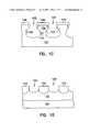
- FIGS. 1A to 1 Dare cross-sectional representations of a method for forming isolated silicon rows.
- FIG. 1Eis a plan view of isolated silicon islands formed on the isolated silicon rows shown in FIG. 1D.
- FIG. 1Fis a cross-sectional representation of NMOS and PMOS transistors formed on the isolated silicon islands shown in FIG. 1E.
- FIG. 1Gis a plan view of the NMOS and PMOS transistors shown in FIG. 1F.
- a silicon substrate 101is directionally-etched to form trenches 102 , leaving rows 104 of silicon protruding from the substrate 101 .
- the silicon rows 104have widths of one micron or less.
- the trench 102 depth and widthare approximately equal to the width of the silicon rows 104 .
- the direction of the etchvaries with the crystal orientation of the substrate 101 . In one embodiment, the etch direction is orthogonal to the plane of the substrate 101 .
- CMOScomplementary metal-oxide-semiconductor
- the direction of the etchis preferably in the ⁇ 100> direction.
- the substrate 101is oxidized at a temperature of approximately 900 to 1,100 degrees Celsius, covered with silicon nitride (Si 3 N 4 ), masked and etched to form exposed oxide regions using standard techniques. Then, the exposed oxide regions are etched away with a directional etchant, preferably a reactive ion etch (RIE), forming trenches 102 in the substrate 101 .
- RIEreactive ion etch
- a Si 3 N 4 cap 106is formed on the silicon rows 104 .
- the Si 3 N 4 106is deposited over the structure, using techniques well known in the art, such as chemical vapor deposition (CVD).
- Si 3 N 4 106forms on the tops of the silicon rows 104 and partly down the sides of the trenches 102 . Material overhang at the top of the trench 102 prevents Si 3 N 4 106 from covering the lower sides of the trenches 102 . However, some Si 3 N 4 106 is deposited onto the bottom of the trenches 102 .
- a photoresist maskis used to cover the silicon rows 104 and an etch is then used to remove residual Si 3 N 4 106 on the bottom of the trenches 102 and then an isotropic chemical etch is used to partially undercut the rows 104 of silicon, as shown in FIG. 1C.
- a standard chemical etch using hydrofluoric acid (HF) or a commercial etchant sold under the trade name CP4 (a mixture of approximately 1 part (46% HF): 1 part (CH 2 COOH):3 parts (HNO 2 ))is used for the isotropic etchant. It is important to use an isotropic etch for this step to compensate for the volume of oxide to be formed in the next step.
- the volume of oxide formedis approximately twice that of the silicon 101 consumed.
- Partially undercutting the silicon rows 104reduces the effective width of the rows 104 to a distance 110 small enough that a relatively short, simple oxidation can fully undercut the silicon rows 104 .
- Fully undercutting the rows 104 of siliconis possible because the width 108 of the rows 104 is one micron or less.
- the substrate 101is then oxidized using a standard silicon processing furnace at a temperature of approximately 900 to 1,100 degrees Celsius, as shown in FIG.1D.
- a wet, oxidizing ambientis used in the furnace chamber to oxidize the exposed silicon regions on the lower part of the trenches 102 in a parallel direction to the surface of the substrate 101 .
- the substrate 101is oxidized for a time period, such that oxide 112 fully undercuts the bottom of the silicon rows 104 , leaving isolated silicon rows 104 .
- narrow, sub-micron rows 104 of silicon and appropriately designed process conditionsgenerally planar structures are formed. The larger volume of oxide fills the trenches 102 between the rows 104 .
- the time period for oxidationdepends on the width 108 of the rows 104 and the effective width 110 after the partial undercut step. As the desired size of the silicon rows 104 decreases, so does the required oxidation time. For example, for sub-micron technology, oxidation time is approximately 3 to 4 hours. For sub-0.25 micron technology, oxidation time is approximately 1 hour.
- Active areas 114are then defined on the individual silicon rows 104 , using a standard process, such as LOCal Oxidation of Silicon (LOCOS), as shown in FIG. 1E, to form oxide 116 between the active areas 114 .
- LOCOSLOCal Oxidation of Silicon
- the area of these active areas 114is approximately one square micron or less for sub-micron technology and approximately 0.0625 square microns or less for sub-0.25 micron technology.
- the resulting isolated active areas 114are not subjected to as much mechanical stress and crystal damage as are active areas formed by prior art techniques of oxidizing to undercut each individual active area, which are excessively stressed and damaged at each corner of the active area.
- Devicesare then formed on the resulting silicon islands 114 , as shown in FIGS. 1F and 1G, according to methods well known in the art.
- a gate oxide layer 118 , source/drain regions 120 , 122 , and a gate 124are formed for each transistor on an individual silicon island 114 .
- source/drain regions 120are doped to form (p+) regions.
- source/drain regions 122are doped to form (n+) regions.
- Further standard process techniquesare then used to connect the devices to form circuits, such as dynamic random access memory (DRAM) devices.
- DRAMdynamic random access memory
- the process described aboveis a low cost, simple method for forming sub-micron SOI devices.
- the methodis compatible with existing large volume manufacturing conditions. Resulting devices are able to formed on semiconductor chips in a highly dense, arrayed manner.
- the inventionenables formation of very high density and very high performance CMOS integrated circuits, DRAMs, as well as other integrated circuits.
Landscapes
- Engineering & Computer Science (AREA)
- Physics & Mathematics (AREA)
- Condensed Matter Physics & Semiconductors (AREA)
- General Physics & Mathematics (AREA)
- Manufacturing & Machinery (AREA)
- Computer Hardware Design (AREA)
- Microelectronics & Electronic Packaging (AREA)
- Power Engineering (AREA)
- Element Separation (AREA)
- Metal-Oxide And Bipolar Metal-Oxide Semiconductor Integrated Circuits (AREA)
Abstract
Description
- The present invention relates to methods and apparatus for isolating semiconductor devices with silicon on insulator technology, and in particular, for forming isolated silicon islands using sub-micron technology.[0001]
- The advantages of silicon on insulator (SOI) technology for complementary metal-oxide-semiconductor (CMOS) integrated circuits (ICs) are well documented. In general, undesired p-n junction capacitance between a source/drain and a substrate is reduced by approximately twenty-five-percent when using SOI technology. Furthermore, active current consumption is less and device access time is equivalent to that of similar devices formed on bulk-silicon substrates. Other advantages of SOI technology include suppression of the short channel effect, suppression of the body-effect, high punch-through immunity, and freedom from latch-up and soft errors. As the demand increases for battery-operated equipment, SOI technology is becoming increasingly more popular due to its low power requirements and high speeds.[0002]
- There are many different techniques for isolating devices in ICs. A technique is selected according to its different attributes, such as: minimum isolation spacing, surface planarity, process complexity, and density of defects generated during fabrication.[0003]
- SIMOX (Separation by IMplanted OXygen) technology is one method for forming SOI structures. SIMOX entails implanting a high dose of oxygen ions at a sufficiently deep level within a silicon substrate. A subsequent anneal step forms a buried oxide layer in the substrate. After the anneal step, an additional layer of epitaxial silicon is usually deposited to obtain a sufficiently thick silicon layer on which to form a device. Disadvantages of using SIMOX include its high expense and yield loss, which undesirably decreases achievable chip density.[0004]
- Another technique for forming an isolation layer in a substrate is by the wafer bonding method. Using this technique, two oxidized silicon wafers are fused together through a high-temperature furnace step. However, this technique increases the substrate thickness, which is often a critical dimension. Furthermore, wafer bonding techniques are often plagued by low production yield due to particles/voids, which prevent adequate bonding between the two wafers in such areas.[0005]
- Another technique used for forming an isolation layer in a substrate is by forming silicon islands through a series of etch and oxidation steps. For example, U.S. Pat. No. 4,604,162 (hereinafter the '162 patent) uses a series of a pad oxide layer, a silicon nitride layer, and a silicon dioxide layer, which is photolithographically masked and anisotropically etched to define silicon islands capped with a silicon nitride layer. Then, a second anisotropic etch (such as a reactive ion etch (RIE)) removes further substrate material between the silicon islands. The depth of the second anisotropic etch is proportional to the width of the silicon islands. A subsequent oxidation step forms silicon dioxide, undercutting the silicon islands and isolating each of them from surrounding regions. However, this technique has not been used commercially because it is too costly and consumes too much time to oxidize an area having an effective width as great as that of the feature size. Another disadvantage of this technique is that the resulting isolated silicon structure has excess mechanical stress and crystal damage at each of its corners, due to oxidation around the entirety of each individual island, which is necessary for its complete isolation. Furthermore, the method described in the patent application requires an additional planarization step, which adds complexity to the fabrication process.[0006]
- There is a need for an effective isolation technique for sub-micron semiconductor technology that is efficient and simple. A primary concern in the fabrication of ICs is simplicity and minimization of process steps. There is a need for an isolation technique that is inexpensive and compatible with large volume CMOS manufacturing technology. Furthermore, an isolation technique, which allows fabrication of highly dense ICs without increasing the dimensions of the IC is needed.[0007]
- Silicon on insulator (SOI) rows and islands are formed for subsequent sub-micron device formation. For example, complementary metal-oxide-semiconductor (CMOS) transistors are later formed on such SOI rows, isolated from each other using standard techniques, such as LOCal Oxidation of Silicon (LOCOS). To form the rows, trenches are directionally-etched in a silicon substrate, leaving rows of silicon between the trenches.[0008]
- Silicon nitride is then deposited over the trenches, extending partly down the sides of the trenches. An isotropic chemical etch is then used to partially undercut narrow rows of silicon in the substrate. It is important to use an isotropic etch for this step to compensate for the volume of oxide to be formed. In general, the volume of oxide formed is approximately twice that of the silicon consumed. Furthermore, an isotropic etch is necessary to advantageously minimize the subsequent oxidation time needed to fully undercut the silicon rows. The subsequent oxidation step fully undercuts the rows of silicon, isolating the silicon rows from adjacent active areas.[0009]
- One advantage of this invention is that by using narrow, sub-micron rows of silicon and appropriately designed process conditions, generally planar structures are formed in an integrated circuit (IC). The larger volume of oxide fills the trenches between the rows. This avoids complex and expensive planarization techniques, such as employed in older micron dimension technologies. Furthermore, such oxidation minimizes mechanical stress and crystal damage in resulting structures, when used to finish undercutting rows, as compared to undercutting individual silicon islands.[0010]
- This invention enables formation of sub-micron devices, such as CMOS transistors, having a high chip density, without increasing the dimensions of the IC. This method yields isolated active regions, having a high degree of regularity and yield, formed in an inexpensive manner. This method is compatible with CMOS IC manufacturing technology due to its simplicity and minimal number of process steps. Regular array structures, such as dynamic random access memories (DRAMs) particularly benefit from this invention, separated on the silicon rows using LOCOS technology.[0011]
- FIGS. 1A to[0012]1D are cross-sectional representations of a method for forming isolated silicon rows.
- FIG. 1E is a plan view of isolated silicon islands formed on the isolated silicon rows shown in FIG. 1D.[0013]
- FIG. 1F is a cross-sectional representation of NMOS and PMOS transistors formed on the isolated silicon islands shown in FIG. 1E.[0014]
- FIG. 1G is a plan view of the NMOS and PMOS transistors shown in FIG. 1F.[0015]
- In the following detailed description, reference is made to the accompanying drawings which form a part hereof, and in which is shown by way of illustration specific embodiments in which the invention may be practiced. These embodiments are described in sufficient detail to enable those skilled in the art to practice the invention, and it is to be understood that other embodiments may be utilized and that structural, logical and electrical changes may be made without departing from the spirit and scope of the present invention. The following detailed description is, therefore, not to be taken in a limiting sense, and the scope of the present invention is defined by the appended claims. Numbering in the Figures is usually done with the hundreds and thousands digits corresponding to the figure number, with the exception that the same components may appear in multiple figures.[0016]
- As shown in FIG. 1A, a[0017]
silicon substrate 101 is directionally-etched to formtrenches 102, leavingrows 104 of silicon protruding from thesubstrate 101. Thesilicon rows 104 have widths of one micron or less. Thetrench 102 depth and width are approximately equal to the width of thesilicon rows 104. The direction of the etch varies with the crystal orientation of thesubstrate 101. In one embodiment, the etch direction is orthogonal to the plane of thesubstrate 101. For complementary metal-oxide-semiconductor (CMOS) devices,substrates 101 having a {100} crystallographic orientation are commonly used due to the ability to achieve small surface state densities on such substrates. Therefore, the direction of the etch is preferably in the <100> direction. To form the trenches, thesubstrate 101 is oxidized at a temperature of approximately 900 to 1,100 degrees Celsius, covered with silicon nitride (Si3N4), masked and etched to form exposed oxide regions using standard techniques. Then, the exposed oxide regions are etched away with a directional etchant, preferably a reactive ion etch (RIE), formingtrenches 102 in thesubstrate 101. - Next, as shown in FIG. 1B, a Si[0018]3N4cap106 is formed on the
silicon rows 104. The Si3N4106 is deposited over the structure, using techniques well known in the art, such as chemical vapor deposition (CVD). Si3N4106 forms on the tops of thesilicon rows 104 and partly down the sides of thetrenches 102. Material overhang at the top of thetrench 102 prevents Si3N4106 from covering the lower sides of thetrenches 102. However, some Si3N4106 is deposited onto the bottom of thetrenches 102. - A photoresist mask is used to cover the[0019]
silicon rows 104 and an etch is then used to remove residual Si3N4106 on the bottom of thetrenches 102 and then an isotropic chemical etch is used to partially undercut therows 104 of silicon, as shown in FIG. 1C. A standard chemical etch using hydrofluoric acid (HF) or a commercial etchant sold under the trade name CP4 (a mixture of approximately 1 part (46% HF): 1 part (CH2COOH):3 parts (HNO2)) is used for the isotropic etchant. It is important to use an isotropic etch for this step to compensate for the volume of oxide to be formed in the next step. In general, the volume of oxide formed is approximately twice that of thesilicon 101 consumed. Partially undercutting thesilicon rows 104, reduces the effective width of therows 104 to adistance 110 small enough that a relatively short, simple oxidation can fully undercut thesilicon rows 104. Fully undercutting therows 104 of silicon is possible because thewidth 108 of therows 104 is one micron or less. - The[0020]
substrate 101 is then oxidized using a standard silicon processing furnace at a temperature of approximately 900 to 1,100 degrees Celsius, as shown in FIG.1D. A wet, oxidizing ambient is used in the furnace chamber to oxidize the exposed silicon regions on the lower part of thetrenches 102 in a parallel direction to the surface of thesubstrate 101. Thesubstrate 101 is oxidized for a time period, such thatoxide 112 fully undercuts the bottom of thesilicon rows 104, leavingisolated silicon rows 104. By using narrow,sub-micron rows 104 of silicon and appropriately designed process conditions, generally planar structures are formed. The larger volume of oxide fills thetrenches 102 between therows 104. This avoids the need for complex and expensive planarization techniques, such as employed in older micron dimension technologies. The time period for oxidation depends on thewidth 108 of therows 104 and theeffective width 110 after the partial undercut step. As the desired size of thesilicon rows 104 decreases, so does the required oxidation time. For example, for sub-micron technology, oxidation time is approximately 3 to 4 hours. For sub-0.25 micron technology, oxidation time is approximately 1 hour. - [0021]
Active areas 114 are then defined on theindividual silicon rows 104, using a standard process, such as LOCal Oxidation of Silicon (LOCOS), as shown in FIG. 1E, to formoxide 116 between theactive areas 114. Depending on the width of thesilicon rows 104, the area of theseactive areas 114 is approximately one square micron or less for sub-micron technology and approximately 0.0625 square microns or less for sub-0.25 micron technology. The resulting isolatedactive areas 114 are not subjected to as much mechanical stress and crystal damage as are active areas formed by prior art techniques of oxidizing to undercut each individual active area, which are excessively stressed and damaged at each corner of the active area. - Devices are then formed on the resulting[0022]
silicon islands 114, as shown in FIGS. 1F and 1G, according to methods well known in the art. For example, when forming CMOS transistors, agate oxide layer 118, source/drain regions gate 124 are formed for each transistor on anindividual silicon island 114. For PMOS transistors, source/drain regions 120 are doped to form (p+) regions. For NMOS transistors, source/drain regions 122 are doped to form (n+) regions. Further standard process techniques are then used to connect the devices to form circuits, such as dynamic random access memory (DRAM) devices. - The process described above is a low cost, simple method for forming sub-micron SOI devices. The method is compatible with existing large volume manufacturing conditions. Resulting devices are able to formed on semiconductor chips in a highly dense, arrayed manner. Thus, the invention enables formation of very high density and very high performance CMOS integrated circuits, DRAMs, as well as other integrated circuits.[0023]
- It should be noted that in CMOS technology, many times certain areas of the semiconductor die described as having a particular doping, could quite easily be of a different doping, promoting a different type of charge carrier. In such instances, if one were to reverse the primary carriers in all areas of the die and adjust for carrier mobility, the invention would operate in the same manner as described herein without departing from the scope and spirit of the present invention.[0024]
- It is to be understood that the above description is intended to be illustrative, and not restrictive. Many other embodiments will be apparent to those of skill in the art upon reviewing the above description. The scope of the invention should, therefore, be determined with reference to the appended claims, along with the full scope of equivalents to which such claims are entitled.[0025]
Claims (20)
1. A method for manufacturing a silicon on insulator substrate, comprising the steps of:
directionally etching a silicon substrate, to form a plurality of trenches between protruding silicon rows;
forming a silicon nitride cap on the silicon rows, extending partway down the sides of the trenches;
isotropically etching the trenches, to partially undercut the silicon rows; and
oxidizing the substrate, to fully undercut the silicon rows.
2. The method ofclaim 1 , wherein the silicon substrate has a {100} crystallographic orientation and the directional etch is in the <100> direction.
3. The method ofclaim 1 , wherein the directional etchant comprises a reactive ion etch.
4. The method ofclaim 1 , wherein the isotropic etchant comprises hydrofluoric acid.
5. The method ofclaim 1 , wherein the silicon rows have a width dimension of one micron or less.
6. The method ofclaim 1 , wherein the silicon rows have a width dimension of 0.25 microns or less.
7. The method ofclaim 1 , wherein the directional etch is approximately as deep as the width of the silicon rows and approximately as wide as the width of the silicon rows.
8. The method ofclaim 1 , wherein the oxidizing step comprises oxidizing the substrate in a wet oxidizing ambient at a temperature of approximately 900 to 1,100 degrees Celsius.
9. The method ofclaim 1 , and further comprising the step of:
defining a plurality of active areas on the silicon rows by local oxidation of silicon.
10. The method ofclaim 9 , and further comprising the step of:
forming a transistor on each of a plurality of the active areas.
11. A silicon on insulator structure, comprising:
a plurality of silicon rows, having a width dimension of one micron or less, embedded in an oxidized substrate; and
a plurality of oxide rows between the silicon rows.
12. The structure ofclaim 11 , wherein the oxide rows have a width dimension of one micron or less.
13. The structure ofclaim 11 , wherein the silicon rows have a width dimension of 0.25 microns or less.
14. The structure ofclaim 11 , wherein the oxide rows have a width dimension of 0.25 microns or less.
15. A plurality of active areas on a semiconductor substrate, comprising:
a plurality of isolated silicon active areas, having an area of one square micron or less, embedded in an oxidized substrate; and
a plurality of oxide rows between the silicon active areas in one direction.
16. The structure ofclaim 15 , and further comprising:
a plurality of transistors formed on each of a plurality of the silicon active areas.
17. The structure ofclaim 15 , wherein the oxide rows have a width dimension of one micron or less.
18. The structure ofclaim 15 , wherein the oxide rows have a width dimension of 0.25 microns or less.
19. The structure ofclaim 15 , wherein the area of the silicon active areas is 0.0625 square microns or less.
20. The structure ofclaim 15 , wherein the active areas are isolated using local oxidation of silicon.
Priority Applications (1)
| Application Number | Priority Date | Filing Date | Title |
|---|---|---|---|
| US08/898,187US20020001965A1 (en) | 1996-09-04 | 1997-07-22 | Technique for producing small islands of silicon on insulator |
Applications Claiming Priority (2)
| Application Number | Priority Date | Filing Date | Title |
|---|---|---|---|
| US08/706,230US5691230A (en) | 1996-09-04 | 1996-09-04 | Technique for producing small islands of silicon on insulator |
| US08/898,187US20020001965A1 (en) | 1996-09-04 | 1997-07-22 | Technique for producing small islands of silicon on insulator |
Related Parent Applications (1)
| Application Number | Title | Priority Date | Filing Date |
|---|---|---|---|
| US08/706,230DivisionUS5691230A (en) | 1996-09-04 | 1996-09-04 | Technique for producing small islands of silicon on insulator |
Publications (1)
| Publication Number | Publication Date |
|---|---|
| US20020001965A1true US20020001965A1 (en) | 2002-01-03 |
Family
ID=24836751
Family Applications (3)
| Application Number | Title | Priority Date | Filing Date |
|---|---|---|---|
| US08/706,230Expired - LifetimeUS5691230A (en) | 1996-09-04 | 1996-09-04 | Technique for producing small islands of silicon on insulator |
| US08/898,187AbandonedUS20020001965A1 (en) | 1996-09-04 | 1997-07-22 | Technique for producing small islands of silicon on insulator |
| US08/970,932Expired - LifetimeUS6174784B1 (en) | 1996-09-04 | 1997-11-14 | Technique for producing small islands of silicon on insulator |
Family Applications Before (1)
| Application Number | Title | Priority Date | Filing Date |
|---|---|---|---|
| US08/706,230Expired - LifetimeUS5691230A (en) | 1996-09-04 | 1996-09-04 | Technique for producing small islands of silicon on insulator |
Family Applications After (1)
| Application Number | Title | Priority Date | Filing Date |
|---|---|---|---|
| US08/970,932Expired - LifetimeUS6174784B1 (en) | 1996-09-04 | 1997-11-14 | Technique for producing small islands of silicon on insulator |
Country Status (1)
| Country | Link |
|---|---|
| US (3) | US5691230A (en) |
Cited By (30)
| Publication number | Priority date | Publication date | Assignee | Title |
|---|---|---|---|---|
| US20020070419A1 (en)* | 2000-12-13 | 2002-06-13 | Farrar Paul A. | Method of forming buried conductor patterns by surface transformation of empty spaces in solid state materials |
| US20030133683A1 (en)* | 2002-01-17 | 2003-07-17 | Micron Technology, Inc. | Three-dimensional photonic crystal waveguide structure and method |
| US20040023874A1 (en)* | 2002-03-15 | 2004-02-05 | Burgess Catherine E. | Therapeutic polypeptides, nucleic acids encoding same, and methods of use |
| US6721956B2 (en)* | 2001-07-17 | 2004-04-13 | Scientific-Atlanta, Inc. | Interactive information services system and associated method for capturing transaction data |
| US20040173798A1 (en)* | 2003-03-05 | 2004-09-09 | Micron Technology, Inc. | Micro-mechanically strained semiconductor film |
| US20040217391A1 (en)* | 2003-04-29 | 2004-11-04 | Micron Technology, Inc. | Localized strained semiconductor on insulator |
| US20040221792A1 (en)* | 2003-05-07 | 2004-11-11 | Micron Technology, Inc. | Strained Si/SiGe structures by ion implantation |
| US20040232487A1 (en)* | 2003-05-21 | 2004-11-25 | Micron Technology, Inc. | Ultra-thin semiconductors bonded on glass substrates |
| US20040232488A1 (en)* | 2003-05-21 | 2004-11-25 | Micron Technology, Inc. | Silicon oxycarbide substrates for bonded silicon on insulator |
| US20040232422A1 (en)* | 2003-05-21 | 2004-11-25 | Micron Technology, Inc. | Wafer gettering using relaxed silicon germanium epitaxial proximity layers |
| US20050020094A1 (en)* | 2003-07-21 | 2005-01-27 | Micron Technology, Inc. | Strained semiconductor by full wafer bonding |
| US20050017273A1 (en)* | 2003-07-21 | 2005-01-27 | Micron Technology, Inc. | Gettering using voids formed by surface transformation |
| US20050032296A1 (en)* | 2003-05-07 | 2005-02-10 | Micron Technology, Inc. | Micromechanical strained semiconductor by wafer bonding |
| US20050029619A1 (en)* | 2003-08-05 | 2005-02-10 | Micron Technology, Inc. | Strained Si/SiGe/SOI islands and processes of making same |
| US20050070036A1 (en)* | 2001-05-16 | 2005-03-31 | Geusic Joseph E. | Method of forming mirrors by surface transformation of empty spaces in solid state materials |
| US20060102979A1 (en)* | 2003-06-18 | 2006-05-18 | Dongbuanam Semiconductor Inc. | STI structure and fabricating methods thereof |
| US20060226480A1 (en)* | 2005-04-06 | 2006-10-12 | International Business Machines Corporation | Method for fabricating oxygen-implanted silicon on insulation type semiconductor and semiconductor formed therefrom |
| US20060258063A1 (en)* | 2003-05-21 | 2006-11-16 | Micron Technology, Inc. | Gettering of silicon on insulator using relaxed silicon germanium epitaxial proximity layers |
| US20080029832A1 (en)* | 2006-08-03 | 2008-02-07 | Micron Technology, Inc. | Bonded strained semiconductor with a desired surface orientation and conductance direction |
| US20080310231A1 (en)* | 2003-12-05 | 2008-12-18 | Cleeves James M | Optimization of critical dimensions and pitch of patterned features in and above a substrate |
| US20090001936A1 (en)* | 2002-11-05 | 2009-01-01 | Mino Green | Structured silicon anode |
| US20090016674A1 (en)* | 2007-07-12 | 2009-01-15 | Shinya Watanabe | Silicon structure and method of manufacturing the same |
| US20090014773A1 (en)* | 2007-07-10 | 2009-01-15 | Ching-Nan Hsiao | Two bit memory structure and method of making the same |
| WO2009095835A2 (en) | 2008-01-31 | 2009-08-06 | Nxp B.V. | Fully insulated semiconductor device and a method of manufacturing the same |
| US20090256243A1 (en)* | 2002-03-25 | 2009-10-15 | Micron Technology, Inc. | Low k interconnect dielectric using surface transformation |
| US20120049318A1 (en)* | 2010-08-30 | 2012-03-01 | Renesas Electronics Corporation | Semiconductor device and manufacturing method thereof |
| US8227309B2 (en) | 2006-02-16 | 2012-07-24 | Micron Technology, Inc. | Localized compressive strained semiconductor |
| DE10250830B4 (en)* | 2002-10-31 | 2015-02-26 | Qimonda Ag | Method for producing a circuit array |
| US9875926B2 (en) | 2015-11-29 | 2018-01-23 | Infineon Technologies Ag | Substrates with buried isolation layers and methods of formation thereof |
| US10410911B2 (en) | 2016-12-13 | 2019-09-10 | Infineon Technologies Ag | Buried insulator regions and methods of formation thereof |
Families Citing this family (91)
| Publication number | Priority date | Publication date | Assignee | Title |
|---|---|---|---|---|
| KR100510232B1 (en)* | 1996-02-21 | 2005-10-27 | 텍사스 인스트루먼츠 인코포레이티드 | How to reduce non-uniformity of refill layer thickness in semiconductor devices |
| US5691230A (en)* | 1996-09-04 | 1997-11-25 | Micron Technology, Inc. | Technique for producing small islands of silicon on insulator |
| US6211039B1 (en)* | 1996-11-12 | 2001-04-03 | Micron Technology, Inc. | Silicon-on-insulator islands and method for their formation |
| KR100230425B1 (en)* | 1997-06-20 | 1999-11-15 | 윤종용 | Method of forming a trench isolation layer having a void |
| US6072209A (en) | 1997-07-08 | 2000-06-06 | Micro Technology, Inc. | Four F2 folded bit line DRAM cell structure having buried bit and word lines |
| US6191470B1 (en) | 1997-07-08 | 2001-02-20 | Micron Technology, Inc. | Semiconductor-on-insulator memory cell with buried word and body lines |
| US6150687A (en) | 1997-07-08 | 2000-11-21 | Micron Technology, Inc. | Memory cell having a vertical transistor with buried source/drain and dual gates |
| US5909618A (en)* | 1997-07-08 | 1999-06-01 | Micron Technology, Inc. | Method of making memory cell with vertical transistor and buried word and body lines |
| US5936274A (en)* | 1997-07-08 | 1999-08-10 | Micron Technology, Inc. | High density flash memory |
| US5973356A (en)* | 1997-07-08 | 1999-10-26 | Micron Technology, Inc. | Ultra high density flash memory |
| US5914511A (en)* | 1997-10-06 | 1999-06-22 | Micron Technology, Inc. | Circuit and method for a folded bit line memory using trench plate capacitor cells with body bias contacts |
| US6528837B2 (en) | 1997-10-06 | 2003-03-04 | Micron Technology, Inc. | Circuit and method for an open bit line memory cell with a vertical transistor and trench plate trench capacitor |
| US5907170A (en)* | 1997-10-06 | 1999-05-25 | Micron Technology, Inc. | Circuit and method for an open bit line memory cell with a vertical transistor and trench plate trench capacitor |
| US6066869A (en)* | 1997-10-06 | 2000-05-23 | Micron Technology, Inc. | Circuit and method for a folded bit line memory cell with vertical transistor and trench capacitor |
| US6025225A (en)* | 1998-01-22 | 2000-02-15 | Micron Technology, Inc. | Circuits with a trench capacitor having micro-roughened semiconductor surfaces and methods for forming the same |
| US6242775B1 (en) | 1998-02-24 | 2001-06-05 | Micron Technology, Inc. | Circuits and methods using vertical complementary transistors |
| US6304483B1 (en) | 1998-02-24 | 2001-10-16 | Micron Technology, Inc. | Circuits and methods for a static random access memory using vertical transistors |
| US5963469A (en)* | 1998-02-24 | 1999-10-05 | Micron Technology, Inc. | Vertical bipolar read access for low voltage memory cell |
| US6246083B1 (en) | 1998-02-24 | 2001-06-12 | Micron Technology, Inc. | Vertical gain cell and array for a dynamic random access memory |
| US6448615B1 (en) | 1998-02-26 | 2002-09-10 | Micron Technology, Inc. | Methods, structures, and circuits for transistors with gate-to-body capacitive coupling |
| US6124729A (en) | 1998-02-27 | 2000-09-26 | Micron Technology, Inc. | Field programmable logic arrays with vertical transistors |
| US5991225A (en)* | 1998-02-27 | 1999-11-23 | Micron Technology, Inc. | Programmable memory address decode array with vertical transistors |
| US6046477A (en)* | 1998-03-17 | 2000-04-04 | Micron Technology, Inc. | Dense SOI programmable logic array structure |
| US6107663A (en)* | 1998-03-30 | 2000-08-22 | Micron Technology, Inc. | Circuit and method for gate-body structures in CMOS technology |
| US6075272A (en)* | 1998-03-30 | 2000-06-13 | Micron Technology, Inc. | Structure for gated lateral bipolar transistors |
| US6229342B1 (en) | 1998-03-30 | 2001-05-08 | Micron Technology, Inc. | Circuits and method for body contacted and backgated transistors |
| US6104066A (en)* | 1998-03-30 | 2000-08-15 | Micron Technology, Inc. | Circuit and method for low voltage, voltage sense amplifier |
| US6049496A (en)* | 1998-03-30 | 2000-04-11 | Micron Technology, Inc. | Circuit and method for low voltage, current sense amplifier |
| US6307235B1 (en) | 1998-03-30 | 2001-10-23 | Micron Technology, Inc. | Another technique for gated lateral bipolar transistors |
| US6097065A (en) | 1998-03-30 | 2000-08-01 | Micron Technology, Inc. | Circuits and methods for dual-gated transistors |
| US6215145B1 (en) | 1998-04-06 | 2001-04-10 | Micron Technology, Inc. | Dense SOI flash memory array structure |
| US6043527A (en) | 1998-04-14 | 2000-03-28 | Micron Technology, Inc. | Circuits and methods for a memory cell with a trench plate trench capacitor and a vertical bipolar read device |
| US6134175A (en) | 1998-08-04 | 2000-10-17 | Micron Technology, Inc. | Memory address decode array with vertical transistors |
| US6093623A (en) | 1998-08-04 | 2000-07-25 | Micron Technology, Inc. | Methods for making silicon-on-insulator structures |
| US6208164B1 (en) | 1998-08-04 | 2001-03-27 | Micron Technology, Inc. | Programmable logic array with vertical transistors |
| US6156589A (en) | 1998-09-03 | 2000-12-05 | Micron Technology, Inc. | Compact SOI body contact link |
| US6194253B1 (en) | 1998-10-07 | 2001-02-27 | International Business Machines Corporation | Method for fabrication of silicon on insulator substrates |
| US6423613B1 (en) | 1998-11-10 | 2002-07-23 | Micron Technology, Inc. | Low temperature silicon wafer bond process with bulk material bond strength |
| EP1049155A1 (en) | 1999-04-29 | 2000-11-02 | STMicroelectronics S.r.l. | Process for manufacturing a SOI wafer with buried oxide regions without cusps |
| US6483171B1 (en)* | 1999-08-13 | 2002-11-19 | Micron Technology, Inc. | Vertical sub-micron CMOS transistors on (110), (111), (311), (511), and higher order surfaces of bulk, SOI and thin film structures and method of forming same |
| US6261876B1 (en)* | 1999-11-04 | 2001-07-17 | International Business Machines Corporation | Planar mixed SOI-bulk substrate for microelectronic applications |
| US6392922B1 (en)* | 2000-08-14 | 2002-05-21 | Micron Technology, Inc. | Passivated magneto-resistive bit structure and passivation method therefor |
| US6437389B1 (en)* | 2000-08-22 | 2002-08-20 | Micron Technology, Inc. | Vertical gate transistors in pass transistor programmable logic arrays |
| US6573154B1 (en)* | 2000-10-26 | 2003-06-03 | Institute Of Microelectronics | High aspect ratio trench isolation process for surface micromachined sensors and actuators |
| US6417033B1 (en)* | 2000-12-19 | 2002-07-09 | Vanguard International Semiconductor Corp. | Method of fabricating a silicon island |
| KR100382612B1 (en)* | 2000-12-29 | 2003-05-09 | 주식회사 하이닉스반도체 | Method for forming the void wafer |
| US6377070B1 (en) | 2001-02-09 | 2002-04-23 | Micron Technology, Inc. | In-service programmable logic arrays with ultra thin vertical body transistors |
| US6448601B1 (en) | 2001-02-09 | 2002-09-10 | Micron Technology, Inc. | Memory address and decode circuits with ultra thin body transistors |
| US6566682B2 (en) | 2001-02-09 | 2003-05-20 | Micron Technology, Inc. | Programmable memory address and decode circuits with ultra thin vertical body transistors |
| US6496034B2 (en) | 2001-02-09 | 2002-12-17 | Micron Technology, Inc. | Programmable logic arrays with ultra thin body transistors |
| US6531727B2 (en) | 2001-02-09 | 2003-03-11 | Micron Technology, Inc. | Open bit line DRAM with ultra thin body transistors |
| US6559491B2 (en)* | 2001-02-09 | 2003-05-06 | Micron Technology, Inc. | Folded bit line DRAM with ultra thin body transistors |
| US6424001B1 (en) | 2001-02-09 | 2002-07-23 | Micron Technology, Inc. | Flash memory with ultra thin vertical body transistors |
| US6649476B2 (en) | 2001-02-15 | 2003-11-18 | Micron Technology, Inc. | Monotonic dynamic-static pseudo-NMOS logic circuit and method of forming a logic gate array |
| US6852167B2 (en) | 2001-03-01 | 2005-02-08 | Micron Technology, Inc. | Methods, systems, and apparatus for uniform chemical-vapor depositions |
| US6597203B2 (en) | 2001-03-14 | 2003-07-22 | Micron Technology, Inc. | CMOS gate array with vertical transistors |
| TW540154B (en)* | 2001-06-04 | 2003-07-01 | Promos Technologies Inc | Deep trench capacitor structure and its manufacturing method |
| US7135734B2 (en)* | 2001-08-30 | 2006-11-14 | Micron Technology, Inc. | Graded composition metal oxide tunnel barrier interpoly insulators |
| US7042043B2 (en) | 2001-08-30 | 2006-05-09 | Micron Technology, Inc. | Programmable array logic or memory devices with asymmetrical tunnel barriers |
| US6963103B2 (en)* | 2001-08-30 | 2005-11-08 | Micron Technology, Inc. | SRAM cells with repressed floating gate memory, low tunnel barrier interpoly insulators |
| US7075829B2 (en) | 2001-08-30 | 2006-07-11 | Micron Technology, Inc. | Programmable memory address and decode circuits with low tunnel barrier interpoly insulators |
| US7068544B2 (en) | 2001-08-30 | 2006-06-27 | Micron Technology, Inc. | Flash memory with low tunnel barrier interpoly insulators |
| US7087954B2 (en) | 2001-08-30 | 2006-08-08 | Micron Technology, Inc. | In service programmable logic arrays with low tunnel barrier interpoly insulators |
| US6778441B2 (en)* | 2001-08-30 | 2004-08-17 | Micron Technology, Inc. | Integrated circuit memory device and method |
| US6754108B2 (en) | 2001-08-30 | 2004-06-22 | Micron Technology, Inc. | DRAM cells with repressed floating gate memory, low tunnel barrier interpoly insulators |
| US7476925B2 (en) | 2001-08-30 | 2009-01-13 | Micron Technology, Inc. | Atomic layer deposition of metal oxide and/or low asymmetrical tunnel barrier interploy insulators |
| US7132711B2 (en) | 2001-08-30 | 2006-11-07 | Micron Technology, Inc. | Programmable array logic or memory with p-channel devices and asymmetrical tunnel barriers |
| US6784480B2 (en)* | 2002-02-12 | 2004-08-31 | Micron Technology, Inc. | Asymmetric band-gap engineered nonvolatile memory device |
| US6784076B2 (en)* | 2002-04-08 | 2004-08-31 | Micron Technology, Inc. | Process for making a silicon-on-insulator ledge by implanting ions from silicon source |
| US7589029B2 (en) | 2002-05-02 | 2009-09-15 | Micron Technology, Inc. | Atomic layer deposition and conversion |
| US7160577B2 (en) | 2002-05-02 | 2007-01-09 | Micron Technology, Inc. | Methods for atomic-layer deposition of aluminum oxides in integrated circuits |
| US6642090B1 (en)* | 2002-06-03 | 2003-11-04 | International Business Machines Corporation | Fin FET devices from bulk semiconductor and method for forming |
| US7045466B2 (en)* | 2002-06-27 | 2006-05-16 | Cornell Research Foundation, Inc. | Three dimensional high aspect ratio micromachining |
| US7221586B2 (en) | 2002-07-08 | 2007-05-22 | Micron Technology, Inc. | Memory utilizing oxide nanolaminates |
| US20040077178A1 (en)* | 2002-10-17 | 2004-04-22 | Applied Materials, Inc. | Method for laterally etching a semiconductor structure |
| JP4167565B2 (en)* | 2003-07-31 | 2008-10-15 | 株式会社東芝 | Method for manufacturing partial SOI substrate |
| JP4473651B2 (en)* | 2004-06-18 | 2010-06-02 | 株式会社東芝 | Manufacturing method of semiconductor device |
| US7247570B2 (en) | 2004-08-19 | 2007-07-24 | Micron Technology, Inc. | Silicon pillars for vertical transistors |
| US7276406B2 (en)* | 2004-10-29 | 2007-10-02 | Freescale Semiconductor, Inc. | Transistor structure with dual trench for optimized stress effect and method therefor |
| US7211474B2 (en)* | 2005-01-18 | 2007-05-01 | International Business Machines Corporation | SOI device with body contact self-aligned to gate |
| US7927948B2 (en) | 2005-07-20 | 2011-04-19 | Micron Technology, Inc. | Devices with nanocrystals and methods of formation |
| US20070249127A1 (en)* | 2006-04-24 | 2007-10-25 | Freescale Semiconductor, Inc. | Electronic device including a semiconductor layer and a sidewall spacer and a process of forming the same |
| US7670895B2 (en) | 2006-04-24 | 2010-03-02 | Freescale Semiconductor, Inc | Process of forming an electronic device including a semiconductor layer and another layer adjacent to an opening within the semiconductor layer |
| US7491622B2 (en)* | 2006-04-24 | 2009-02-17 | Freescale Semiconductor, Inc. | Process of forming an electronic device including a layer formed using an inductively coupled plasma |
| US7528078B2 (en) | 2006-05-12 | 2009-05-05 | Freescale Semiconductor, Inc. | Process of forming electronic device including a densified nitride layer adjacent to an opening within a semiconductor layer |
| US8026571B2 (en)* | 2008-05-29 | 2011-09-27 | United Microelectronics Corp. | Semiconductor-device isolation structure |
| KR101221871B1 (en)* | 2009-12-07 | 2013-01-15 | 한국전자통신연구원 | method for manufacturing semiconductor device |
| EP2455967B1 (en) | 2010-11-18 | 2018-05-23 | IMEC vzw | A method for forming a buried dielectric layer underneath a semiconductor fin |
| KR102111738B1 (en)* | 2013-06-05 | 2020-05-15 | 삼성전자주식회사 | Memory device, memory system and operating method of the same |
| US9299609B2 (en)* | 2014-07-23 | 2016-03-29 | Seagate Technology Llc | Hard-mask defined bit pattern substrate |
| US10410910B1 (en)* | 2018-08-20 | 2019-09-10 | Nanya Technology Corporation | Method for preparing semiconductor structures |
Family Cites Families (28)
| Publication number | Priority date | Publication date | Assignee | Title |
|---|---|---|---|---|
| US3407479A (en) | 1965-06-28 | 1968-10-29 | Motorola Inc | Isolation of semiconductor devices |
| US3471754A (en) | 1966-03-26 | 1969-10-07 | Sony Corp | Isolation structure for integrated circuits |
| US3689357A (en) | 1970-12-10 | 1972-09-05 | Gen Motors Corp | Glass-polysilicon dielectric isolation |
| US4419150A (en) | 1980-12-29 | 1983-12-06 | Rockwell International Corporation | Method of forming lateral bipolar transistors |
| US4437226A (en)* | 1981-03-02 | 1984-03-20 | Rockwell International Corporation | Process for producing NPN type lateral transistor with minimal substrate operation interference |
| US4625391A (en) | 1981-06-23 | 1986-12-02 | Tokyo Shibaura Denki Kabushiki Kaisha | Semiconductor device and method for manufacturing the same |
| US4580331A (en)* | 1981-07-01 | 1986-04-08 | Rockwell International Corporation | PNP-type lateral transistor with minimal substrate operation interference and method for producing same |
| US4604162A (en)* | 1983-06-13 | 1986-08-05 | Ncr Corporation | Formation and planarization of silicon-on-insulator structures |
| US4615746A (en)* | 1983-09-29 | 1986-10-07 | Kenji Kawakita | Method of forming isolated island regions in a semiconductor substrate by selective etching and oxidation and devices formed therefrom |
| FR2554638A1 (en)* | 1983-11-04 | 1985-05-10 | Efcis | METHOD FOR MANUFACTURING INTEGRATED SILICON STRUCTURES ON ISOLATED ISOLES OF THE SUBSTRATE |
| US4763183A (en) | 1984-08-01 | 1988-08-09 | American Telephone And Telegraph Co., At&T Bell Laboratories | Semiconductor-on-insulator (SOI) devices and SOI IC fabrication method |
| US4685198A (en)* | 1985-07-25 | 1987-08-11 | Matsushita Electric Industrial Co., Ltd. | Method of manufacturing isolated semiconductor devices |
| US4755481A (en) | 1986-05-15 | 1988-07-05 | General Electric Company | Method of making a silicon-on-insulator transistor |
| JPH0779133B2 (en) | 1986-06-12 | 1995-08-23 | 松下電器産業株式会社 | Method for manufacturing semiconductor device |
| JPH01125858A (en) | 1987-11-10 | 1989-05-18 | Fujitsu Ltd | Semiconductor device and manufacture thereof |
| US5177028A (en) | 1991-10-22 | 1993-01-05 | Micron Technology, Inc. | Trench isolation method having a double polysilicon gate formed on mesas |
| US5528062A (en)* | 1992-06-17 | 1996-06-18 | International Business Machines Corporation | High-density DRAM structure on soi |
| US5234535A (en) | 1992-12-10 | 1993-08-10 | International Business Machines Corporation | Method of producing a thin silicon-on-insulator layer |
| US5306659A (en)* | 1993-03-29 | 1994-04-26 | International Business Machines Corporation | Reach-through isolation etching method for silicon-on-insulator devices |
| US5426070A (en) | 1993-05-26 | 1995-06-20 | Cornell Research Foundation, Inc. | Microstructures and high temperature isolation process for fabrication thereof |
| US5441591A (en) | 1993-06-07 | 1995-08-15 | The United States Of America As Represented By The Secretary Of The Navy | Silicon to sapphire bond |
| US5492853A (en) | 1994-03-11 | 1996-02-20 | Micron Semiconductor, Inc. | Method of forming a contact using a trench and an insulation layer during the formation of a semiconductor device |
| US5440158A (en) | 1994-07-05 | 1995-08-08 | Taiwan Semiconductor Manufacturing Company Ltd. | Electrically programmable memory device with improved dual floating gates |
| JP2806277B2 (en) | 1994-10-13 | 1998-09-30 | 日本電気株式会社 | Semiconductor device and manufacturing method thereof |
| US5497017A (en) | 1995-01-26 | 1996-03-05 | Micron Technology, Inc. | Dynamic random access memory array having a cross-point layout, tungsten digit lines buried in the substrate, and vertical access transistors |
| US5640342A (en) | 1995-11-20 | 1997-06-17 | Micron Technology, Inc. | Structure for cross coupled thin film transistors and static random access memory cell |
| US5710057A (en) | 1996-07-12 | 1998-01-20 | Kenney; Donald M. | SOI fabrication method |
| US5691230A (en)* | 1996-09-04 | 1997-11-25 | Micron Technology, Inc. | Technique for producing small islands of silicon on insulator |
- 1996
- 1996-09-04USUS08/706,230patent/US5691230A/ennot_activeExpired - Lifetime
- 1997
- 1997-07-22USUS08/898,187patent/US20020001965A1/ennot_activeAbandoned
- 1997-11-14USUS08/970,932patent/US6174784B1/ennot_activeExpired - Lifetime
Cited By (91)
| Publication number | Priority date | Publication date | Assignee | Title |
|---|---|---|---|---|
| US20020070419A1 (en)* | 2000-12-13 | 2002-06-13 | Farrar Paul A. | Method of forming buried conductor patterns by surface transformation of empty spaces in solid state materials |
| US7164188B2 (en) | 2000-12-13 | 2007-01-16 | Micron Technology, Inc. | Buried conductor patterns formed by surface transformation of empty spaces in solid state materials |
| US7512170B2 (en) | 2001-05-16 | 2009-03-31 | Micron Technology, Inc. | Method of forming mirrors by surface transformation of empty spaces in solid state materials |
| US7260125B2 (en) | 2001-05-16 | 2007-08-21 | Micron Technology, Inc. | Method of forming mirrors by surface transformation of empty spaces in solid state materials |
| US20050175058A1 (en)* | 2001-05-16 | 2005-08-11 | Geusic Joseph E. | Method of forming mirrors by surface transformation of empty spaces in solid state materials |
| US7142577B2 (en) | 2001-05-16 | 2006-11-28 | Micron Technology, Inc. | Method of forming mirrors by surface transformation of empty spaces in solid state materials and structures thereon |
| US20050070036A1 (en)* | 2001-05-16 | 2005-03-31 | Geusic Joseph E. | Method of forming mirrors by surface transformation of empty spaces in solid state materials |
| US20070036196A1 (en)* | 2001-05-16 | 2007-02-15 | Geusic Joseph E | Method of forming mirrors by surface transformation of empty spaces in solid state materials |
| US7054532B2 (en) | 2001-05-22 | 2006-05-30 | Micron Technoloy. Inc. | Three-dimensional photonic crystal waveguide structure and method |
| US20050105869A1 (en)* | 2001-05-22 | 2005-05-19 | Micron Technology, Inc. | Three-dimensional photonic crystal waveguide structure and method |
| US6721956B2 (en)* | 2001-07-17 | 2004-04-13 | Scientific-Atlanta, Inc. | Interactive information services system and associated method for capturing transaction data |
| US20030133683A1 (en)* | 2002-01-17 | 2003-07-17 | Micron Technology, Inc. | Three-dimensional photonic crystal waveguide structure and method |
| US6898362B2 (en) | 2002-01-17 | 2005-05-24 | Micron Technology Inc. | Three-dimensional photonic crystal waveguide structure and method |
| US20040023874A1 (en)* | 2002-03-15 | 2004-02-05 | Burgess Catherine E. | Therapeutic polypeptides, nucleic acids encoding same, and methods of use |
| US20090256243A1 (en)* | 2002-03-25 | 2009-10-15 | Micron Technology, Inc. | Low k interconnect dielectric using surface transformation |
| DE10250830B4 (en)* | 2002-10-31 | 2015-02-26 | Qimonda Ag | Method for producing a circuit array |
| US20090001936A1 (en)* | 2002-11-05 | 2009-01-01 | Mino Green | Structured silicon anode |
| US7842535B2 (en) | 2002-11-05 | 2010-11-30 | Nexeon Ltd. | Structured silicon anode |
| US20040173798A1 (en)* | 2003-03-05 | 2004-09-09 | Micron Technology, Inc. | Micro-mechanically strained semiconductor film |
| US7405444B2 (en) | 2003-03-05 | 2008-07-29 | Micron Technology, Inc. | Micro-mechanically strained semiconductor film |
| US7202530B2 (en) | 2003-03-05 | 2007-04-10 | Micron Technology, Inc. | Micro-mechanically strained semiconductor film |
| US20070164361A1 (en)* | 2003-03-05 | 2007-07-19 | Micron Technology, Inc. | Micro-mechanically strained semiconductor film |
| US7198974B2 (en) | 2003-03-05 | 2007-04-03 | Micron Technology, Inc. | Micro-mechanically strained semiconductor film |
| US20060011982A1 (en)* | 2003-03-05 | 2006-01-19 | Micron Technology, Inc. | Micro-mechanically strained semiconductor film |
| US20040217391A1 (en)* | 2003-04-29 | 2004-11-04 | Micron Technology, Inc. | Localized strained semiconductor on insulator |
| US7041575B2 (en) | 2003-04-29 | 2006-05-09 | Micron Technology, Inc. | Localized strained semiconductor on insulator |
| US7394111B2 (en) | 2003-05-07 | 2008-07-01 | Micron Technology, Inc. | Strained Si/SiGe structures by ion implantation |
| US6987037B2 (en) | 2003-05-07 | 2006-01-17 | Micron Technology, Inc. | Strained Si/SiGe structures by ion implantation |
| US7045874B2 (en) | 2003-05-07 | 2006-05-16 | Micron Technology, Inc. | Micromechanical strained semiconductor by wafer bonding |
| US20050285139A1 (en)* | 2003-05-07 | 2005-12-29 | Micron Technology, Inc. | Strained Si/SiGe structures by ion implantation |
| US20050032296A1 (en)* | 2003-05-07 | 2005-02-10 | Micron Technology, Inc. | Micromechanical strained semiconductor by wafer bonding |
| US7115480B2 (en) | 2003-05-07 | 2006-10-03 | Micron Technology, Inc. | Micromechanical strained semiconductor by wafer bonding |
| US7482190B2 (en) | 2003-05-07 | 2009-01-27 | Micron Technology, Inc. | Micromechanical strained semiconductor by wafer bonding |
| US20040221792A1 (en)* | 2003-05-07 | 2004-11-11 | Micron Technology, Inc. | Strained Si/SiGe structures by ion implantation |
| US20060001094A1 (en)* | 2003-05-21 | 2006-01-05 | Micron Technology, Inc. | Semiconductor on insulator structure |
| US7687329B2 (en) | 2003-05-21 | 2010-03-30 | Micron Technology, Inc. | Gettering of silicon on insulator using relaxed silicon germanium epitaxial proximity layers |
| US20040232487A1 (en)* | 2003-05-21 | 2004-11-25 | Micron Technology, Inc. | Ultra-thin semiconductors bonded on glass substrates |
| US20060263994A1 (en)* | 2003-05-21 | 2006-11-23 | Micron Technology, Inc. | Semiconductors bonded on glass substrates |
| US20060258063A1 (en)* | 2003-05-21 | 2006-11-16 | Micron Technology, Inc. | Gettering of silicon on insulator using relaxed silicon germanium epitaxial proximity layers |
| US20040232488A1 (en)* | 2003-05-21 | 2004-11-25 | Micron Technology, Inc. | Silicon oxycarbide substrates for bonded silicon on insulator |
| US7501329B2 (en) | 2003-05-21 | 2009-03-10 | Micron Technology, Inc. | Wafer gettering using relaxed silicon germanium epitaxial proximity layers |
| US7504310B2 (en) | 2003-05-21 | 2009-03-17 | Micron Technology, Inc. | Semiconductors bonded on glass substrates |
| US7008854B2 (en) | 2003-05-21 | 2006-03-07 | Micron Technology, Inc. | Silicon oxycarbide substrates for bonded silicon on insulator |
| US7662701B2 (en) | 2003-05-21 | 2010-02-16 | Micron Technology, Inc. | Gettering of silicon on insulator using relaxed silicon germanium epitaxial proximity layers |
| US20040232422A1 (en)* | 2003-05-21 | 2004-11-25 | Micron Technology, Inc. | Wafer gettering using relaxed silicon germanium epitaxial proximity layers |
| US7528463B2 (en) | 2003-05-21 | 2009-05-05 | Micron Technolgy, Inc. | Semiconductor on insulator structure |
| US7271445B2 (en) | 2003-05-21 | 2007-09-18 | Micron Technology, Inc. | Ultra-thin semiconductors bonded on glass substrates |
| US7273788B2 (en) | 2003-05-21 | 2007-09-25 | Micron Technology, Inc. | Ultra-thin semiconductors bonded on glass substrates |
| US7391096B2 (en)* | 2003-06-18 | 2008-06-24 | Dongbu Electronics Co., Ltd. | STI structure |
| US20060102979A1 (en)* | 2003-06-18 | 2006-05-18 | Dongbuanam Semiconductor Inc. | STI structure and fabricating methods thereof |
| US7994595B2 (en) | 2003-07-21 | 2011-08-09 | Micron Technology, Inc. | Strained semiconductor by full wafer bonding |
| US6929984B2 (en) | 2003-07-21 | 2005-08-16 | Micron Technology Inc. | Gettering using voids formed by surface transformation |
| US8470687B2 (en) | 2003-07-21 | 2013-06-25 | Micron Technology, Inc. | Strained semiconductor by full wafer bonding |
| US7989311B2 (en) | 2003-07-21 | 2011-08-02 | Micron Technlogy, Inc. | Strained semiconductor by full wafer bonding |
| US20050029683A1 (en)* | 2003-07-21 | 2005-02-10 | Micron Technology, Inc. | Gettering using voids formed by surface transformation |
| US7439158B2 (en) | 2003-07-21 | 2008-10-21 | Micron Technology, Inc. | Strained semiconductor by full wafer bonding |
| US20070075401A1 (en)* | 2003-07-21 | 2007-04-05 | Micron Technology, Inc. | Gettering using voids formed by surface transformation |
| US20050250274A1 (en)* | 2003-07-21 | 2005-11-10 | Micron Technology, Inc. | Gettering using voids formed by surface transformation |
| US7564082B2 (en) | 2003-07-21 | 2009-07-21 | Micron Technology, Inc. | Gettering using voids formed by surface transformation |
| US7544984B2 (en) | 2003-07-21 | 2009-06-09 | Micron Technology, Inc. | Gettering using voids formed by surface transformation |
| US20050017273A1 (en)* | 2003-07-21 | 2005-01-27 | Micron Technology, Inc. | Gettering using voids formed by surface transformation |
| US20090042360A1 (en)* | 2003-07-21 | 2009-02-12 | Micron Technology Inc. | Strained semiconductor by full wafer bonding |
| US20050020094A1 (en)* | 2003-07-21 | 2005-01-27 | Micron Technology, Inc. | Strained semiconductor by full wafer bonding |
| US7326597B2 (en) | 2003-07-21 | 2008-02-05 | Micron Technology, Inc. | Gettering using voids formed by surface transformation |
| US20050029619A1 (en)* | 2003-08-05 | 2005-02-10 | Micron Technology, Inc. | Strained Si/SiGe/SOI islands and processes of making same |
| US20060267152A1 (en)* | 2003-08-05 | 2006-11-30 | Micron Technology, Inc. | Strained Si/SiGe/SOI islands and processes of making same |
| US7525164B2 (en) | 2003-08-05 | 2009-04-28 | Micron Technology, Inc. | Strained Si/SiGe/SOI islands and processes of making same |
| US7262428B2 (en) | 2003-08-05 | 2007-08-28 | Micron Technology, Inc. | Strained Si/SiGe/SOI islands and processes of making same |
| US20050087842A1 (en)* | 2003-08-05 | 2005-04-28 | Micron Technology, Inc. | Strained Si/SiGe/SOI islands and processes of making same |
| US20080078988A1 (en)* | 2003-08-05 | 2008-04-03 | Micron Technology, Inc. | Strained Si/SiGe/SOI islands and processes of making same |
| US7153753B2 (en) | 2003-08-05 | 2006-12-26 | Micron Technology, Inc. | Strained Si/SiGe/SOI islands and processes of making same |
| US7368790B2 (en) | 2003-08-05 | 2008-05-06 | Micron Technology, Inc. | Strained Si/SiGe/SOI islands and processes of making same |
| US20080310231A1 (en)* | 2003-12-05 | 2008-12-18 | Cleeves James M | Optimization of critical dimensions and pitch of patterned features in and above a substrate |
| US8283706B2 (en)* | 2003-12-05 | 2012-10-09 | Sandisk 3D Llc | Optimization of critical dimensions and pitch of patterned features in and above a substrate |
| US8766332B2 (en) | 2003-12-05 | 2014-07-01 | Sandisk 3D Llc | Optimization of critical dimensions and pitch of patterned features in and above a substrate |
| US7504314B2 (en) | 2005-04-06 | 2009-03-17 | International Business Machines Corporation | Method for fabricating oxygen-implanted silicon on insulation type semiconductor and semiconductor formed therefrom |
| US20060226480A1 (en)* | 2005-04-06 | 2006-10-12 | International Business Machines Corporation | Method for fabricating oxygen-implanted silicon on insulation type semiconductor and semiconductor formed therefrom |
| US8435850B2 (en) | 2006-02-16 | 2013-05-07 | Micron Technology, Inc. | Localized compressive strained semiconductor |
| US8227309B2 (en) | 2006-02-16 | 2012-07-24 | Micron Technology, Inc. | Localized compressive strained semiconductor |
| US20080029832A1 (en)* | 2006-08-03 | 2008-02-07 | Micron Technology, Inc. | Bonded strained semiconductor with a desired surface orientation and conductance direction |
| US8962447B2 (en) | 2006-08-03 | 2015-02-24 | Micron Technology, Inc. | Bonded strained semiconductor with a desired surface orientation and conductance direction |
| US20090014773A1 (en)* | 2007-07-10 | 2009-01-15 | Ching-Nan Hsiao | Two bit memory structure and method of making the same |
| US20090016674A1 (en)* | 2007-07-12 | 2009-01-15 | Shinya Watanabe | Silicon structure and method of manufacturing the same |
| US20100320513A1 (en)* | 2008-01-31 | 2010-12-23 | Nxp B.V. | Semiconductor device and a method of manufacturing the same |
| WO2009095835A2 (en) | 2008-01-31 | 2009-08-06 | Nxp B.V. | Fully insulated semiconductor device and a method of manufacturing the same |
| US8110455B2 (en) | 2008-01-31 | 2012-02-07 | Nxp B.V. | Semiconductor device and a method of manufacturing the same |
| US8710619B2 (en)* | 2010-08-30 | 2014-04-29 | Renesas Electronics Corporation | Semiconductor device and manufacturing method thereof |
| US20120049318A1 (en)* | 2010-08-30 | 2012-03-01 | Renesas Electronics Corporation | Semiconductor device and manufacturing method thereof |
| US9875926B2 (en) | 2015-11-29 | 2018-01-23 | Infineon Technologies Ag | Substrates with buried isolation layers and methods of formation thereof |
| US10410911B2 (en) | 2016-12-13 | 2019-09-10 | Infineon Technologies Ag | Buried insulator regions and methods of formation thereof |
| DE102016124207B4 (en) | 2016-12-13 | 2023-04-27 | Infineon Technologies Ag | METHOD OF FORMING BURIED ISOLATION AREAS |
Also Published As
| Publication number | Publication date |
|---|---|
| US6174784B1 (en) | 2001-01-16 |
| US5691230A (en) | 1997-11-25 |
Similar Documents
| Publication | Publication Date | Title |
|---|---|---|
| US5691230A (en) | Technique for producing small islands of silicon on insulator | |
| US6211039B1 (en) | Silicon-on-insulator islands and method for their formation | |
| US7394131B2 (en) | STI formation in semiconductor device including SOI and bulk silicon regions | |
| US6214694B1 (en) | Process of making densely patterned silicon-on-insulator (SOI) region on a wafer | |
| US6001706A (en) | Method for making improved shallow trench isolation for semiconductor integrated circuits | |
| JP4322453B2 (en) | Semiconductor device and manufacturing method thereof | |
| US5989977A (en) | Shallow trench isolation process | |
| US9355887B2 (en) | Dual trench isolation for CMOS with hybrid orientations | |
| US6350662B1 (en) | Method to reduce defects in shallow trench isolations by post liner anneal | |
| KR100238244B1 (en) | Method of trench isolation | |
| US20030013323A1 (en) | Method of selective removal of SiGe alloys | |
| US5436173A (en) | Method for forming a semiconductor on insulator device | |
| US6335267B1 (en) | Semiconductor substrate and method of fabricating semiconductor device | |
| US6074932A (en) | Method for forming a stress-free shallow trench isolation | |
| US20100096701A1 (en) | Semiconductor Device and Method of Manufacturing the Same | |
| US7202123B1 (en) | Mesa isolation technology for extremely thin silicon-on-insulator semiconductor devices | |
| US6215145B1 (en) | Dense SOI flash memory array structure | |
| US5264387A (en) | Method of forming uniformly thin, isolated silicon mesas on an insulating substrate | |
| US6046477A (en) | Dense SOI programmable logic array structure | |
| US6331470B1 (en) | Process for manufacturing a semiconductor material wafer having power regions dielectrically insulated from circuitry regions | |
| GB2309585A (en) | A method of fabricating a SOI substrate | |
| KR100552827B1 (en) | Manufacturing Method of High Voltage Semiconductor Device Forming Deep Well and Gate Oxide Simultaneously | |
| KR100708798B1 (en) | Semiconductor substrate, semiconductor device, method for manufacturing semiconductor substrate, and method for manufacturing semiconductor device | |
| JP3321527B2 (en) | Method for manufacturing semiconductor device | |
| KR19990015463A (en) | Trench element isolation method for semiconductor devices |
Legal Events
| Date | Code | Title | Description |
|---|---|---|---|
| STCB | Information on status: application discontinuation | Free format text:ABANDONED -- AFTER EXAMINER'S ANSWER OR BOARD OF APPEALS DECISION |