US20020000665A1 - Semiconductor device conductive bump and interconnect barrier - Google Patents
Semiconductor device conductive bump and interconnect barrierDownload PDFInfo
- Publication number
- US20020000665A1 US20020000665A1US09/285,666US28566699AUS2002000665A1US 20020000665 A1US20020000665 A1US 20020000665A1US 28566699 AUS28566699 AUS 28566699AUS 2002000665 A1US2002000665 A1US 2002000665A1
- Authority
- US
- United States
- Prior art keywords
- layer
- barrier layer
- semiconductor device
- interconnect
- conductive barrier
- Prior art date
- Legal status (The legal status is an assumption and is not a legal conclusion. Google has not performed a legal analysis and makes no representation as to the accuracy of the status listed.)
- Abandoned
Links
- 230000004888barrier functionEffects0.000titleclaimsabstractdescription101
- 239000004065semiconductorSubstances0.000titleclaimsabstractdescription47
- 238000002161passivationMethods0.000claimsabstractdescription49
- 239000000758substrateSubstances0.000claimsabstractdescription11
- 239000000463materialSubstances0.000claimsdescription40
- 238000000034methodMethods0.000claimsdescription35
- RYGMFSIKBFXOCR-UHFFFAOYSA-NCopperChemical compound[Cu]RYGMFSIKBFXOCR-UHFFFAOYSA-N0.000claimsdescription30
- 229910052802copperInorganic materials0.000claimsdescription30
- 239000010949copperSubstances0.000claimsdescription30
- 230000003647oxidationEffects0.000claimsdescription25
- 238000007254oxidation reactionMethods0.000claimsdescription25
- IJGRMHOSHXDMSA-UHFFFAOYSA-NAtomic nitrogenChemical compoundN#NIJGRMHOSHXDMSA-UHFFFAOYSA-N0.000claimsdescription11
- PXHVJJICTQNCMI-UHFFFAOYSA-NNickelChemical compound[Ni]PXHVJJICTQNCMI-UHFFFAOYSA-N0.000claimsdescription9
- XUIMIQQOPSSXEZ-UHFFFAOYSA-NSiliconChemical group[Si]XUIMIQQOPSSXEZ-UHFFFAOYSA-N0.000claimsdescription9
- 229910052710siliconInorganic materials0.000claimsdescription9
- 239000010703siliconSubstances0.000claimsdescription9
- 239000003870refractory metalSubstances0.000claimsdescription7
- 239000010936titaniumSubstances0.000claimsdescription7
- RTAQQCXQSZGOHL-UHFFFAOYSA-NTitaniumChemical compound[Ti]RTAQQCXQSZGOHL-UHFFFAOYSA-N0.000claimsdescription6
- 229910052719titaniumInorganic materials0.000claimsdescription6
- 150000004767nitridesChemical class0.000claimsdescription5
- 229910052757nitrogenInorganic materials0.000claimsdescription5
- 229910052759nickelInorganic materials0.000claimsdescription4
- 238000005530etchingMethods0.000claimsdescription3
- 229910052741iridiumInorganic materials0.000claimsdescription3
- GKOZUEZYRPOHIO-UHFFFAOYSA-Niridium atomChemical compound[Ir]GKOZUEZYRPOHIO-UHFFFAOYSA-N0.000claimsdescription3
- 229910052715tantalumInorganic materials0.000claimsdescription3
- GUVRBAGPIYLISA-UHFFFAOYSA-Ntantalum atomChemical compound[Ta]GUVRBAGPIYLISA-UHFFFAOYSA-N0.000claimsdescription3
- WFKWXMTUELFFGS-UHFFFAOYSA-NtungstenChemical compound[W]WFKWXMTUELFFGS-UHFFFAOYSA-N0.000claimsdescription3
- 229910052721tungstenInorganic materials0.000claimsdescription3
- 239000010937tungstenSubstances0.000claimsdescription3
- 229910052751metalInorganic materials0.000description22
- 239000002184metalSubstances0.000description22
- 230000008569processEffects0.000description21
- 229910000679solderInorganic materials0.000description8
- 230000008901benefitEffects0.000description7
- CSCPPACGZOOCGX-UHFFFAOYSA-NAcetoneChemical compoundCC(C)=OCSCPPACGZOOCGX-UHFFFAOYSA-N0.000description6
- VYZAMTAEIAYCRO-UHFFFAOYSA-NChromiumChemical compound[Cr]VYZAMTAEIAYCRO-UHFFFAOYSA-N0.000description6
- 229910052581Si3N4Inorganic materials0.000description6
- LQBJWKCYZGMFEV-UHFFFAOYSA-Nlead tinChemical compound[Sn].[Pb]LQBJWKCYZGMFEV-UHFFFAOYSA-N0.000description6
- HQVNEWCFYHHQES-UHFFFAOYSA-Nsilicon nitrideChemical compoundN12[Si]34N5[Si]62N3[Si]51N64HQVNEWCFYHHQES-UHFFFAOYSA-N0.000description6
- QVGXLLKOCUKJST-UHFFFAOYSA-Natomic oxygenChemical compound[O]QVGXLLKOCUKJST-UHFFFAOYSA-N0.000description5
- 229910052804chromiumInorganic materials0.000description5
- 239000011651chromiumSubstances0.000description5
- 230000009977dual effectEffects0.000description5
- PCHJSUWPFVWCPO-UHFFFAOYSA-NgoldChemical compound[Au]PCHJSUWPFVWCPO-UHFFFAOYSA-N0.000description5
- 229910052737goldInorganic materials0.000description5
- 239000010931goldSubstances0.000description5
- 229910000881Cu alloyInorganic materials0.000description4
- SECXISVLQFMRJM-UHFFFAOYSA-NN-MethylpyrrolidoneChemical compoundCN1CCCC1=OSECXISVLQFMRJM-UHFFFAOYSA-N0.000description4
- NRTOMJZYCJJWKI-UHFFFAOYSA-NTitanium nitrideChemical compound[Ti]#NNRTOMJZYCJJWKI-UHFFFAOYSA-N0.000description4
- 229910052760oxygenInorganic materials0.000description4
- 239000001301oxygenSubstances0.000description4
- 238000000059patterningMethods0.000description4
- NTIZESTWPVYFNL-UHFFFAOYSA-NMethyl isobutyl ketoneChemical compoundCC(C)CC(C)=ONTIZESTWPVYFNL-UHFFFAOYSA-N0.000description3
- UIHCLUNTQKBZGK-UHFFFAOYSA-NMethyl isobutyl ketoneNatural productsCCC(C)C(C)=OUIHCLUNTQKBZGK-UHFFFAOYSA-N0.000description3
- KDLHZDBZIXYQEI-UHFFFAOYSA-NPalladiumChemical compound[Pd]KDLHZDBZIXYQEI-UHFFFAOYSA-N0.000description3
- ZTXONRUJVYXVTJ-UHFFFAOYSA-Nchromium copperChemical compound[Cr][Cu][Cr]ZTXONRUJVYXVTJ-UHFFFAOYSA-N0.000description3
- 239000002131composite materialSubstances0.000description3
- 238000000151depositionMethods0.000description3
- 239000001995intermetallic alloySubstances0.000description3
- 229910044991metal oxideInorganic materials0.000description3
- 150000004706metal oxidesChemical class0.000description3
- 210000002381plasmaAnatomy0.000description3
- 238000007747platingMethods0.000description3
- BASFCYQUMIYNBI-UHFFFAOYSA-NplatinumChemical compound[Pt]BASFCYQUMIYNBI-UHFFFAOYSA-N0.000description3
- 229920001721polyimidePolymers0.000description3
- 239000000126substanceSubstances0.000description3
- OKTJSMMVPCPJKN-UHFFFAOYSA-NCarbonChemical compound[C]OKTJSMMVPCPJKN-UHFFFAOYSA-N0.000description2
- VYPSYNLAJGMNEJ-UHFFFAOYSA-NSilicium dioxideChemical compoundO=[Si]=OVYPSYNLAJGMNEJ-UHFFFAOYSA-N0.000description2
- ATJFFYVFTNAWJD-UHFFFAOYSA-NTinChemical compound[Sn]ATJFFYVFTNAWJD-UHFFFAOYSA-N0.000description2
- 230000004075alterationEffects0.000description2
- 230000015572biosynthetic processEffects0.000description2
- 229910052799carbonInorganic materials0.000description2
- 238000007772electroless platingMethods0.000description2
- 238000009713electroplatingMethods0.000description2
- 230000008020evaporationEffects0.000description2
- 238000001704evaporationMethods0.000description2
- 230000010354integrationEffects0.000description2
- 150000002739metalsChemical class0.000description2
- 238000012986modificationMethods0.000description2
- 230000004048modificationEffects0.000description2
- 229910000487osmium oxideInorganic materials0.000description2
- 238000004806packaging method and processMethods0.000description2
- 238000005240physical vapour depositionMethods0.000description2
- MZLGASXMSKOWSE-UHFFFAOYSA-Ntantalum nitrideChemical compound[Ta]#NMZLGASXMSKOWSE-UHFFFAOYSA-N0.000description2
- WGTYBPLFGIVFAS-UHFFFAOYSA-Mtetramethylammonium hydroxideChemical compound[OH-].C[N+](C)(C)CWGTYBPLFGIVFAS-UHFFFAOYSA-M0.000description2
- -1titanium tungsten nitrideChemical class0.000description2
- ZAMOUSCENKQFHK-UHFFFAOYSA-NChlorine atomChemical compound[Cl]ZAMOUSCENKQFHK-UHFFFAOYSA-N0.000description1
- 229910000599Cr alloyInorganic materials0.000description1
- PXGOKWXKJXAPGV-UHFFFAOYSA-NFluorineChemical compoundFFPXGOKWXKJXAPGV-UHFFFAOYSA-N0.000description1
- FYYHWMGAXLPEAU-UHFFFAOYSA-NMagnesiumChemical compound[Mg]FYYHWMGAXLPEAU-UHFFFAOYSA-N0.000description1
- 239000004642PolyimideSubstances0.000description1
- 229910019599ReO2Inorganic materials0.000description1
- 229910002785ReO3Inorganic materials0.000description1
- KJTLSVCANCCWHF-UHFFFAOYSA-NRutheniumChemical compound[Ru]KJTLSVCANCCWHF-UHFFFAOYSA-N0.000description1
- NINIDFKCEFEMDL-UHFFFAOYSA-NSulfurChemical compound[S]NINIDFKCEFEMDL-UHFFFAOYSA-N0.000description1
- 230000002411adverseEffects0.000description1
- 238000005275alloyingMethods0.000description1
- 229910021417amorphous siliconInorganic materials0.000description1
- 230000003064anti-oxidating effectEffects0.000description1
- 238000004380ashingMethods0.000description1
- GPBUGPUPKAGMDK-UHFFFAOYSA-NazanylidynemolybdenumChemical compound[Mo]#NGPBUGPUPKAGMDK-UHFFFAOYSA-N0.000description1
- IVHJCRXBQPGLOV-UHFFFAOYSA-NazanylidynetungstenChemical compound[W]#NIVHJCRXBQPGLOV-UHFFFAOYSA-N0.000description1
- 238000005229chemical vapour depositionMethods0.000description1
- 239000000460chlorineSubstances0.000description1
- 229910052801chlorineInorganic materials0.000description1
- 239000000788chromium alloySubstances0.000description1
- 238000004140cleaningMethods0.000description1
- 229910017052cobaltInorganic materials0.000description1
- 239000010941cobaltSubstances0.000description1
- 238000007796conventional methodMethods0.000description1
- 230000008878couplingEffects0.000description1
- 238000010168coupling processMethods0.000description1
- 238000005859coupling reactionMethods0.000description1
- 230000007547defectEffects0.000description1
- 230000008021depositionEffects0.000description1
- HTXDPTMKBJXEOW-UHFFFAOYSA-NdioxoiridiumChemical compoundO=[Ir]=OHTXDPTMKBJXEOW-UHFFFAOYSA-N0.000description1
- 239000011737fluorineSubstances0.000description1
- 229910052731fluorineInorganic materials0.000description1
- 239000012535impuritySubstances0.000description1
- 238000011065in-situ storageMethods0.000description1
- 239000011810insulating materialSubstances0.000description1
- 239000012212insulatorSubstances0.000description1
- 230000001788irregularEffects0.000description1
- 238000002955isolationMethods0.000description1
- 239000011777magnesiumSubstances0.000description1
- 229910052749magnesiumInorganic materials0.000description1
- 229910052762osmiumInorganic materials0.000description1
- SYQBFIAQOQZEGI-UHFFFAOYSA-Nosmium atomChemical compound[Os]SYQBFIAQOQZEGI-UHFFFAOYSA-N0.000description1
- JIWAALDUIFCBLV-UHFFFAOYSA-NoxoosmiumChemical compound[Os]=OJIWAALDUIFCBLV-UHFFFAOYSA-N0.000description1
- DYIZHKNUQPHNJY-UHFFFAOYSA-NoxorheniumChemical compound[Re]=ODYIZHKNUQPHNJY-UHFFFAOYSA-N0.000description1
- 229910052763palladiumInorganic materials0.000description1
- 230000002093peripheral effectEffects0.000description1
- 229910052697platinumInorganic materials0.000description1
- 229910021420polycrystalline siliconInorganic materials0.000description1
- 229920005591polysiliconPolymers0.000description1
- 229910052702rheniumInorganic materials0.000description1
- WUAPFZMCVAUBPE-UHFFFAOYSA-Nrhenium atomChemical compound[Re]WUAPFZMCVAUBPE-UHFFFAOYSA-N0.000description1
- 229910003449rhenium oxideInorganic materials0.000description1
- YSZJKUDBYALHQE-UHFFFAOYSA-Nrhenium trioxideChemical compoundO=[Re](=O)=OYSZJKUDBYALHQE-UHFFFAOYSA-N0.000description1
- 229910052707rutheniumInorganic materials0.000description1
- WOCIAKWEIIZHES-UHFFFAOYSA-Nruthenium(iv) oxideChemical compoundO=[Ru]=OWOCIAKWEIIZHES-UHFFFAOYSA-N0.000description1
- 239000000377silicon dioxideSubstances0.000description1
- 235000012239silicon dioxideNutrition0.000description1
- 238000004544sputter depositionMethods0.000description1
- 229910052717sulfurInorganic materials0.000description1
- 239000011593sulfurSubstances0.000description1
- MAKDTFFYCIMFQP-UHFFFAOYSA-Ntitanium tungstenChemical compound[Ti].[W]MAKDTFFYCIMFQP-UHFFFAOYSA-N0.000description1
- 238000007704wet chemistry methodMethods0.000description1
Images


Classifications
- H—ELECTRICITY
- H01—ELECTRIC ELEMENTS
- H01L—SEMICONDUCTOR DEVICES NOT COVERED BY CLASS H10
- H01L21/00—Processes or apparatus adapted for the manufacture or treatment of semiconductor or solid state devices or of parts thereof
- H01L21/70—Manufacture or treatment of devices consisting of a plurality of solid state components formed in or on a common substrate or of parts thereof; Manufacture of integrated circuit devices or of parts thereof
- H01L21/71—Manufacture of specific parts of devices defined in group H01L21/70
- H01L21/768—Applying interconnections to be used for carrying current between separate components within a device comprising conductors and dielectrics
- H01L21/76838—Applying interconnections to be used for carrying current between separate components within a device comprising conductors and dielectrics characterised by the formation and the after-treatment of the conductors
- H01L21/76841—Barrier, adhesion or liner layers
- H01L21/76843—Barrier, adhesion or liner layers formed in openings in a dielectric
- H01L21/76849—Barrier, adhesion or liner layers formed in openings in a dielectric the layer being positioned on top of the main fill metal
- H—ELECTRICITY
- H01—ELECTRIC ELEMENTS
- H01L—SEMICONDUCTOR DEVICES NOT COVERED BY CLASS H10
- H01L21/00—Processes or apparatus adapted for the manufacture or treatment of semiconductor or solid state devices or of parts thereof
- H01L21/70—Manufacture or treatment of devices consisting of a plurality of solid state components formed in or on a common substrate or of parts thereof; Manufacture of integrated circuit devices or of parts thereof
- H01L21/71—Manufacture of specific parts of devices defined in group H01L21/70
- H01L21/768—Applying interconnections to be used for carrying current between separate components within a device comprising conductors and dielectrics
- H01L21/76801—Applying interconnections to be used for carrying current between separate components within a device comprising conductors and dielectrics characterised by the formation and the after-treatment of the dielectrics, e.g. smoothing
- H01L21/76802—Applying interconnections to be used for carrying current between separate components within a device comprising conductors and dielectrics characterised by the formation and the after-treatment of the dielectrics, e.g. smoothing by forming openings in dielectrics
- H01L21/76807—Applying interconnections to be used for carrying current between separate components within a device comprising conductors and dielectrics characterised by the formation and the after-treatment of the dielectrics, e.g. smoothing by forming openings in dielectrics for dual damascene structures
- H01L21/76813—Applying interconnections to be used for carrying current between separate components within a device comprising conductors and dielectrics characterised by the formation and the after-treatment of the dielectrics, e.g. smoothing by forming openings in dielectrics for dual damascene structures involving a partial via etch
- H—ELECTRICITY
- H01—ELECTRIC ELEMENTS
- H01L—SEMICONDUCTOR DEVICES NOT COVERED BY CLASS H10
- H01L21/00—Processes or apparatus adapted for the manufacture or treatment of semiconductor or solid state devices or of parts thereof
- H01L21/70—Manufacture or treatment of devices consisting of a plurality of solid state components formed in or on a common substrate or of parts thereof; Manufacture of integrated circuit devices or of parts thereof
- H01L21/71—Manufacture of specific parts of devices defined in group H01L21/70
- H01L21/768—Applying interconnections to be used for carrying current between separate components within a device comprising conductors and dielectrics
- H01L21/76838—Applying interconnections to be used for carrying current between separate components within a device comprising conductors and dielectrics characterised by the formation and the after-treatment of the conductors
- H01L21/76841—Barrier, adhesion or liner layers
- H01L21/76843—Barrier, adhesion or liner layers formed in openings in a dielectric
- H—ELECTRICITY
- H01—ELECTRIC ELEMENTS
- H01L—SEMICONDUCTOR DEVICES NOT COVERED BY CLASS H10
- H01L21/00—Processes or apparatus adapted for the manufacture or treatment of semiconductor or solid state devices or of parts thereof
- H01L21/70—Manufacture or treatment of devices consisting of a plurality of solid state components formed in or on a common substrate or of parts thereof; Manufacture of integrated circuit devices or of parts thereof
- H01L21/71—Manufacture of specific parts of devices defined in group H01L21/70
- H01L21/768—Applying interconnections to be used for carrying current between separate components within a device comprising conductors and dielectrics
- H01L21/76838—Applying interconnections to be used for carrying current between separate components within a device comprising conductors and dielectrics characterised by the formation and the after-treatment of the conductors
- H01L21/76877—Filling of holes, grooves or trenches, e.g. vias, with conductive material
- H—ELECTRICITY
- H01—ELECTRIC ELEMENTS
- H01L—SEMICONDUCTOR DEVICES NOT COVERED BY CLASS H10
- H01L23/00—Details of semiconductor or other solid state devices
- H01L23/52—Arrangements for conducting electric current within the device in operation from one component to another, i.e. interconnections, e.g. wires, lead frames
- H01L23/522—Arrangements for conducting electric current within the device in operation from one component to another, i.e. interconnections, e.g. wires, lead frames including external interconnections consisting of a multilayer structure of conductive and insulating layers inseparably formed on the semiconductor body
- H01L23/532—Arrangements for conducting electric current within the device in operation from one component to another, i.e. interconnections, e.g. wires, lead frames including external interconnections consisting of a multilayer structure of conductive and insulating layers inseparably formed on the semiconductor body characterised by the materials
- H01L23/53204—Conductive materials
- H01L23/53209—Conductive materials based on metals, e.g. alloys, metal silicides
- H01L23/53228—Conductive materials based on metals, e.g. alloys, metal silicides the principal metal being copper
- H01L23/53233—Copper alloys
- H—ELECTRICITY
- H01—ELECTRIC ELEMENTS
- H01L—SEMICONDUCTOR DEVICES NOT COVERED BY CLASS H10
- H01L23/00—Details of semiconductor or other solid state devices
- H01L23/52—Arrangements for conducting electric current within the device in operation from one component to another, i.e. interconnections, e.g. wires, lead frames
- H01L23/522—Arrangements for conducting electric current within the device in operation from one component to another, i.e. interconnections, e.g. wires, lead frames including external interconnections consisting of a multilayer structure of conductive and insulating layers inseparably formed on the semiconductor body
- H01L23/532—Arrangements for conducting electric current within the device in operation from one component to another, i.e. interconnections, e.g. wires, lead frames including external interconnections consisting of a multilayer structure of conductive and insulating layers inseparably formed on the semiconductor body characterised by the materials
- H01L23/53204—Conductive materials
- H01L23/53209—Conductive materials based on metals, e.g. alloys, metal silicides
- H01L23/53228—Conductive materials based on metals, e.g. alloys, metal silicides the principal metal being copper
- H01L23/53238—Additional layers associated with copper layers, e.g. adhesion, barrier, cladding layers
- H—ELECTRICITY
- H01—ELECTRIC ELEMENTS
- H01L—SEMICONDUCTOR DEVICES NOT COVERED BY CLASS H10
- H01L24/00—Arrangements for connecting or disconnecting semiconductor or solid-state bodies; Methods or apparatus related thereto
- H01L24/01—Means for bonding being attached to, or being formed on, the surface to be connected, e.g. chip-to-package, die-attach, "first-level" interconnects; Manufacturing methods related thereto
- H01L24/02—Bonding areas ; Manufacturing methods related thereto
- H01L24/04—Structure, shape, material or disposition of the bonding areas prior to the connecting process
- H01L24/05—Structure, shape, material or disposition of the bonding areas prior to the connecting process of an individual bonding area
- H—ELECTRICITY
- H01—ELECTRIC ELEMENTS
- H01L—SEMICONDUCTOR DEVICES NOT COVERED BY CLASS H10
- H01L24/00—Arrangements for connecting or disconnecting semiconductor or solid-state bodies; Methods or apparatus related thereto
- H01L24/01—Means for bonding being attached to, or being formed on, the surface to be connected, e.g. chip-to-package, die-attach, "first-level" interconnects; Manufacturing methods related thereto
- H01L24/10—Bump connectors ; Manufacturing methods related thereto
- H01L24/11—Manufacturing methods
- H—ELECTRICITY
- H01—ELECTRIC ELEMENTS
- H01L—SEMICONDUCTOR DEVICES NOT COVERED BY CLASS H10
- H01L2223/00—Details relating to semiconductor or other solid state devices covered by the group H01L23/00
- H01L2223/544—Marks applied to semiconductor devices or parts
- H01L2223/54473—Marks applied to semiconductor devices or parts for use after dicing
- H—ELECTRICITY
- H01—ELECTRIC ELEMENTS
- H01L—SEMICONDUCTOR DEVICES NOT COVERED BY CLASS H10
- H01L2224/00—Indexing scheme for arrangements for connecting or disconnecting semiconductor or solid-state bodies and methods related thereto as covered by H01L24/00
- H01L2224/01—Means for bonding being attached to, or being formed on, the surface to be connected, e.g. chip-to-package, die-attach, "first-level" interconnects; Manufacturing methods related thereto
- H01L2224/02—Bonding areas; Manufacturing methods related thereto
- H01L2224/03—Manufacturing methods
- H01L2224/03001—Involving a temporary auxiliary member not forming part of the manufacturing apparatus, e.g. removable or sacrificial coating, film or substrate
- H01L2224/03009—Involving a temporary auxiliary member not forming part of the manufacturing apparatus, e.g. removable or sacrificial coating, film or substrate for protecting parts during manufacture
- H—ELECTRICITY
- H01—ELECTRIC ELEMENTS
- H01L—SEMICONDUCTOR DEVICES NOT COVERED BY CLASS H10
- H01L2224/00—Indexing scheme for arrangements for connecting or disconnecting semiconductor or solid-state bodies and methods related thereto as covered by H01L24/00
- H01L2224/01—Means for bonding being attached to, or being formed on, the surface to be connected, e.g. chip-to-package, die-attach, "first-level" interconnects; Manufacturing methods related thereto
- H01L2224/02—Bonding areas; Manufacturing methods related thereto
- H01L2224/04—Structure, shape, material or disposition of the bonding areas prior to the connecting process
- H01L2224/05—Structure, shape, material or disposition of the bonding areas prior to the connecting process of an individual bonding area
- H01L2224/05001—Internal layers
- H01L2224/05005—Structure
- H01L2224/05008—Bonding area integrally formed with a redistribution layer on the semiconductor or solid-state body, e.g.
- H—ELECTRICITY
- H01—ELECTRIC ELEMENTS
- H01L—SEMICONDUCTOR DEVICES NOT COVERED BY CLASS H10
- H01L2224/00—Indexing scheme for arrangements for connecting or disconnecting semiconductor or solid-state bodies and methods related thereto as covered by H01L24/00
- H01L2224/01—Means for bonding being attached to, or being formed on, the surface to be connected, e.g. chip-to-package, die-attach, "first-level" interconnects; Manufacturing methods related thereto
- H01L2224/02—Bonding areas; Manufacturing methods related thereto
- H01L2224/04—Structure, shape, material or disposition of the bonding areas prior to the connecting process
- H01L2224/05—Structure, shape, material or disposition of the bonding areas prior to the connecting process of an individual bonding area
- H01L2224/05001—Internal layers
- H01L2224/0502—Disposition
- H01L2224/05024—Disposition the internal layer being disposed on a redistribution layer on the semiconductor or solid-state body
- H—ELECTRICITY
- H01—ELECTRIC ELEMENTS
- H01L—SEMICONDUCTOR DEVICES NOT COVERED BY CLASS H10
- H01L2224/00—Indexing scheme for arrangements for connecting or disconnecting semiconductor or solid-state bodies and methods related thereto as covered by H01L24/00
- H01L2224/01—Means for bonding being attached to, or being formed on, the surface to be connected, e.g. chip-to-package, die-attach, "first-level" interconnects; Manufacturing methods related thereto
- H01L2224/02—Bonding areas; Manufacturing methods related thereto
- H01L2224/04—Structure, shape, material or disposition of the bonding areas prior to the connecting process
- H01L2224/05—Structure, shape, material or disposition of the bonding areas prior to the connecting process of an individual bonding area
- H01L2224/05001—Internal layers
- H01L2224/0502—Disposition
- H01L2224/05025—Disposition the internal layer being disposed on a via connection of the semiconductor or solid-state body
- H—ELECTRICITY
- H01—ELECTRIC ELEMENTS
- H01L—SEMICONDUCTOR DEVICES NOT COVERED BY CLASS H10
- H01L2224/00—Indexing scheme for arrangements for connecting or disconnecting semiconductor or solid-state bodies and methods related thereto as covered by H01L24/00
- H01L2224/01—Means for bonding being attached to, or being formed on, the surface to be connected, e.g. chip-to-package, die-attach, "first-level" interconnects; Manufacturing methods related thereto
- H01L2224/02—Bonding areas; Manufacturing methods related thereto
- H01L2224/04—Structure, shape, material or disposition of the bonding areas prior to the connecting process
- H01L2224/05—Structure, shape, material or disposition of the bonding areas prior to the connecting process of an individual bonding area
- H01L2224/05001—Internal layers
- H01L2224/0502—Disposition
- H01L2224/05026—Disposition the internal layer being disposed in a recess of the surface
- H01L2224/05027—Disposition the internal layer being disposed in a recess of the surface the internal layer extending out of an opening
- H—ELECTRICITY
- H01—ELECTRIC ELEMENTS
- H01L—SEMICONDUCTOR DEVICES NOT COVERED BY CLASS H10
- H01L2224/00—Indexing scheme for arrangements for connecting or disconnecting semiconductor or solid-state bodies and methods related thereto as covered by H01L24/00
- H01L2224/01—Means for bonding being attached to, or being formed on, the surface to be connected, e.g. chip-to-package, die-attach, "first-level" interconnects; Manufacturing methods related thereto
- H01L2224/02—Bonding areas; Manufacturing methods related thereto
- H01L2224/04—Structure, shape, material or disposition of the bonding areas prior to the connecting process
- H01L2224/05—Structure, shape, material or disposition of the bonding areas prior to the connecting process of an individual bonding area
- H01L2224/05001—Internal layers
- H01L2224/05075—Plural internal layers
- H01L2224/0508—Plural internal layers being stacked
- H—ELECTRICITY
- H01—ELECTRIC ELEMENTS
- H01L—SEMICONDUCTOR DEVICES NOT COVERED BY CLASS H10
- H01L2224/00—Indexing scheme for arrangements for connecting or disconnecting semiconductor or solid-state bodies and methods related thereto as covered by H01L24/00
- H01L2224/01—Means for bonding being attached to, or being formed on, the surface to be connected, e.g. chip-to-package, die-attach, "first-level" interconnects; Manufacturing methods related thereto
- H01L2224/02—Bonding areas; Manufacturing methods related thereto
- H01L2224/04—Structure, shape, material or disposition of the bonding areas prior to the connecting process
- H01L2224/05—Structure, shape, material or disposition of the bonding areas prior to the connecting process of an individual bonding area
- H01L2224/05001—Internal layers
- H01L2224/05099—Material
- H01L2224/051—Material with a principal constituent of the material being a metal or a metalloid, e.g. boron [B], silicon [Si], germanium [Ge], arsenic [As], antimony [Sb], tellurium [Te] and polonium [Po], and alloys thereof
- H01L2224/05138—Material with a principal constituent of the material being a metal or a metalloid, e.g. boron [B], silicon [Si], germanium [Ge], arsenic [As], antimony [Sb], tellurium [Te] and polonium [Po], and alloys thereof the principal constituent melting at a temperature of greater than or equal to 950°C and less than 1550°C
- H01L2224/05147—Copper [Cu] as principal constituent
- H—ELECTRICITY
- H01—ELECTRIC ELEMENTS
- H01L—SEMICONDUCTOR DEVICES NOT COVERED BY CLASS H10
- H01L2224/00—Indexing scheme for arrangements for connecting or disconnecting semiconductor or solid-state bodies and methods related thereto as covered by H01L24/00
- H01L2224/01—Means for bonding being attached to, or being formed on, the surface to be connected, e.g. chip-to-package, die-attach, "first-level" interconnects; Manufacturing methods related thereto
- H01L2224/02—Bonding areas; Manufacturing methods related thereto
- H01L2224/04—Structure, shape, material or disposition of the bonding areas prior to the connecting process
- H01L2224/05—Structure, shape, material or disposition of the bonding areas prior to the connecting process of an individual bonding area
- H01L2224/05001—Internal layers
- H01L2224/05099—Material
- H01L2224/051—Material with a principal constituent of the material being a metal or a metalloid, e.g. boron [B], silicon [Si], germanium [Ge], arsenic [As], antimony [Sb], tellurium [Te] and polonium [Po], and alloys thereof
- H01L2224/05138—Material with a principal constituent of the material being a metal or a metalloid, e.g. boron [B], silicon [Si], germanium [Ge], arsenic [As], antimony [Sb], tellurium [Te] and polonium [Po], and alloys thereof the principal constituent melting at a temperature of greater than or equal to 950°C and less than 1550°C
- H01L2224/05157—Cobalt [Co] as principal constituent
- H—ELECTRICITY
- H01—ELECTRIC ELEMENTS
- H01L—SEMICONDUCTOR DEVICES NOT COVERED BY CLASS H10
- H01L2224/00—Indexing scheme for arrangements for connecting or disconnecting semiconductor or solid-state bodies and methods related thereto as covered by H01L24/00
- H01L2224/01—Means for bonding being attached to, or being formed on, the surface to be connected, e.g. chip-to-package, die-attach, "first-level" interconnects; Manufacturing methods related thereto
- H01L2224/02—Bonding areas; Manufacturing methods related thereto
- H01L2224/04—Structure, shape, material or disposition of the bonding areas prior to the connecting process
- H01L2224/05—Structure, shape, material or disposition of the bonding areas prior to the connecting process of an individual bonding area
- H01L2224/05001—Internal layers
- H01L2224/05099—Material
- H01L2224/051—Material with a principal constituent of the material being a metal or a metalloid, e.g. boron [B], silicon [Si], germanium [Ge], arsenic [As], antimony [Sb], tellurium [Te] and polonium [Po], and alloys thereof
- H01L2224/05163—Material with a principal constituent of the material being a metal or a metalloid, e.g. boron [B], silicon [Si], germanium [Ge], arsenic [As], antimony [Sb], tellurium [Te] and polonium [Po], and alloys thereof the principal constituent melting at a temperature of greater than 1550°C
- H01L2224/05166—Titanium [Ti] as principal constituent
- H—ELECTRICITY
- H01—ELECTRIC ELEMENTS
- H01L—SEMICONDUCTOR DEVICES NOT COVERED BY CLASS H10
- H01L2224/00—Indexing scheme for arrangements for connecting or disconnecting semiconductor or solid-state bodies and methods related thereto as covered by H01L24/00
- H01L2224/01—Means for bonding being attached to, or being formed on, the surface to be connected, e.g. chip-to-package, die-attach, "first-level" interconnects; Manufacturing methods related thereto
- H01L2224/02—Bonding areas; Manufacturing methods related thereto
- H01L2224/04—Structure, shape, material or disposition of the bonding areas prior to the connecting process
- H01L2224/05—Structure, shape, material or disposition of the bonding areas prior to the connecting process of an individual bonding area
- H01L2224/05001—Internal layers
- H01L2224/05099—Material
- H01L2224/051—Material with a principal constituent of the material being a metal or a metalloid, e.g. boron [B], silicon [Si], germanium [Ge], arsenic [As], antimony [Sb], tellurium [Te] and polonium [Po], and alloys thereof
- H01L2224/05163—Material with a principal constituent of the material being a metal or a metalloid, e.g. boron [B], silicon [Si], germanium [Ge], arsenic [As], antimony [Sb], tellurium [Te] and polonium [Po], and alloys thereof the principal constituent melting at a temperature of greater than 1550°C
- H01L2224/05172—Vanadium [V] as principal constituent
- H—ELECTRICITY
- H01—ELECTRIC ELEMENTS
- H01L—SEMICONDUCTOR DEVICES NOT COVERED BY CLASS H10
- H01L2224/00—Indexing scheme for arrangements for connecting or disconnecting semiconductor or solid-state bodies and methods related thereto as covered by H01L24/00
- H01L2224/01—Means for bonding being attached to, or being formed on, the surface to be connected, e.g. chip-to-package, die-attach, "first-level" interconnects; Manufacturing methods related thereto
- H01L2224/02—Bonding areas; Manufacturing methods related thereto
- H01L2224/04—Structure, shape, material or disposition of the bonding areas prior to the connecting process
- H01L2224/05—Structure, shape, material or disposition of the bonding areas prior to the connecting process of an individual bonding area
- H01L2224/05001—Internal layers
- H01L2224/05099—Material
- H01L2224/051—Material with a principal constituent of the material being a metal or a metalloid, e.g. boron [B], silicon [Si], germanium [Ge], arsenic [As], antimony [Sb], tellurium [Te] and polonium [Po], and alloys thereof
- H01L2224/05163—Material with a principal constituent of the material being a metal or a metalloid, e.g. boron [B], silicon [Si], germanium [Ge], arsenic [As], antimony [Sb], tellurium [Te] and polonium [Po], and alloys thereof the principal constituent melting at a temperature of greater than 1550°C
- H01L2224/0518—Molybdenum [Mo] as principal constituent
- H—ELECTRICITY
- H01—ELECTRIC ELEMENTS
- H01L—SEMICONDUCTOR DEVICES NOT COVERED BY CLASS H10
- H01L2224/00—Indexing scheme for arrangements for connecting or disconnecting semiconductor or solid-state bodies and methods related thereto as covered by H01L24/00
- H01L2224/01—Means for bonding being attached to, or being formed on, the surface to be connected, e.g. chip-to-package, die-attach, "first-level" interconnects; Manufacturing methods related thereto
- H01L2224/02—Bonding areas; Manufacturing methods related thereto
- H01L2224/04—Structure, shape, material or disposition of the bonding areas prior to the connecting process
- H01L2224/05—Structure, shape, material or disposition of the bonding areas prior to the connecting process of an individual bonding area
- H01L2224/05001—Internal layers
- H01L2224/05099—Material
- H01L2224/051—Material with a principal constituent of the material being a metal or a metalloid, e.g. boron [B], silicon [Si], germanium [Ge], arsenic [As], antimony [Sb], tellurium [Te] and polonium [Po], and alloys thereof
- H01L2224/05163—Material with a principal constituent of the material being a metal or a metalloid, e.g. boron [B], silicon [Si], germanium [Ge], arsenic [As], antimony [Sb], tellurium [Te] and polonium [Po], and alloys thereof the principal constituent melting at a temperature of greater than 1550°C
- H01L2224/05181—Tantalum [Ta] as principal constituent
- H—ELECTRICITY
- H01—ELECTRIC ELEMENTS
- H01L—SEMICONDUCTOR DEVICES NOT COVERED BY CLASS H10
- H01L2224/00—Indexing scheme for arrangements for connecting or disconnecting semiconductor or solid-state bodies and methods related thereto as covered by H01L24/00
- H01L2224/01—Means for bonding being attached to, or being formed on, the surface to be connected, e.g. chip-to-package, die-attach, "first-level" interconnects; Manufacturing methods related thereto
- H01L2224/02—Bonding areas; Manufacturing methods related thereto
- H01L2224/04—Structure, shape, material or disposition of the bonding areas prior to the connecting process
- H01L2224/05—Structure, shape, material or disposition of the bonding areas prior to the connecting process of an individual bonding area
- H01L2224/05001—Internal layers
- H01L2224/05099—Material
- H01L2224/051—Material with a principal constituent of the material being a metal or a metalloid, e.g. boron [B], silicon [Si], germanium [Ge], arsenic [As], antimony [Sb], tellurium [Te] and polonium [Po], and alloys thereof
- H01L2224/05163—Material with a principal constituent of the material being a metal or a metalloid, e.g. boron [B], silicon [Si], germanium [Ge], arsenic [As], antimony [Sb], tellurium [Te] and polonium [Po], and alloys thereof the principal constituent melting at a temperature of greater than 1550°C
- H01L2224/05184—Tungsten [W] as principal constituent
- H—ELECTRICITY
- H01—ELECTRIC ELEMENTS
- H01L—SEMICONDUCTOR DEVICES NOT COVERED BY CLASS H10
- H01L2224/00—Indexing scheme for arrangements for connecting or disconnecting semiconductor or solid-state bodies and methods related thereto as covered by H01L24/00
- H01L2224/01—Means for bonding being attached to, or being formed on, the surface to be connected, e.g. chip-to-package, die-attach, "first-level" interconnects; Manufacturing methods related thereto
- H01L2224/02—Bonding areas; Manufacturing methods related thereto
- H01L2224/04—Structure, shape, material or disposition of the bonding areas prior to the connecting process
- H01L2224/05—Structure, shape, material or disposition of the bonding areas prior to the connecting process of an individual bonding area
- H01L2224/05001—Internal layers
- H01L2224/05099—Material
- H01L2224/05186—Material with a principal constituent of the material being a non metallic, non metalloid inorganic material
- H—ELECTRICITY
- H01—ELECTRIC ELEMENTS
- H01L—SEMICONDUCTOR DEVICES NOT COVERED BY CLASS H10
- H01L2224/00—Indexing scheme for arrangements for connecting or disconnecting semiconductor or solid-state bodies and methods related thereto as covered by H01L24/00
- H01L2224/01—Means for bonding being attached to, or being formed on, the surface to be connected, e.g. chip-to-package, die-attach, "first-level" interconnects; Manufacturing methods related thereto
- H01L2224/02—Bonding areas; Manufacturing methods related thereto
- H01L2224/04—Structure, shape, material or disposition of the bonding areas prior to the connecting process
- H01L2224/05—Structure, shape, material or disposition of the bonding areas prior to the connecting process of an individual bonding area
- H01L2224/0554—External layer
- H01L2224/0556—Disposition
- H01L2224/05571—Disposition the external layer being disposed in a recess of the surface
- H01L2224/05572—Disposition the external layer being disposed in a recess of the surface the external layer extending out of an opening
- H—ELECTRICITY
- H01—ELECTRIC ELEMENTS
- H01L—SEMICONDUCTOR DEVICES NOT COVERED BY CLASS H10
- H01L2224/00—Indexing scheme for arrangements for connecting or disconnecting semiconductor or solid-state bodies and methods related thereto as covered by H01L24/00
- H01L2224/01—Means for bonding being attached to, or being formed on, the surface to be connected, e.g. chip-to-package, die-attach, "first-level" interconnects; Manufacturing methods related thereto
- H01L2224/10—Bump connectors; Manufacturing methods related thereto
- H01L2224/12—Structure, shape, material or disposition of the bump connectors prior to the connecting process
- H01L2224/13—Structure, shape, material or disposition of the bump connectors prior to the connecting process of an individual bump connector
- H01L2224/13001—Core members of the bump connector
- H01L2224/13099—Material
- H01L2224/131—Material with a principal constituent of the material being a metal or a metalloid, e.g. boron [B], silicon [Si], germanium [Ge], arsenic [As], antimony [Sb], tellurium [Te] and polonium [Po], and alloys thereof
- H01L2224/13101—Material with a principal constituent of the material being a metal or a metalloid, e.g. boron [B], silicon [Si], germanium [Ge], arsenic [As], antimony [Sb], tellurium [Te] and polonium [Po], and alloys thereof the principal constituent melting at a temperature of less than 400°C
- H01L2224/13111—Tin [Sn] as principal constituent
- H—ELECTRICITY
- H01—ELECTRIC ELEMENTS
- H01L—SEMICONDUCTOR DEVICES NOT COVERED BY CLASS H10
- H01L24/00—Arrangements for connecting or disconnecting semiconductor or solid-state bodies; Methods or apparatus related thereto
- H01L24/01—Means for bonding being attached to, or being formed on, the surface to be connected, e.g. chip-to-package, die-attach, "first-level" interconnects; Manufacturing methods related thereto
- H01L24/02—Bonding areas ; Manufacturing methods related thereto
- H01L24/03—Manufacturing methods
- H—ELECTRICITY
- H01—ELECTRIC ELEMENTS
- H01L—SEMICONDUCTOR DEVICES NOT COVERED BY CLASS H10
- H01L24/00—Arrangements for connecting or disconnecting semiconductor or solid-state bodies; Methods or apparatus related thereto
- H01L24/01—Means for bonding being attached to, or being formed on, the surface to be connected, e.g. chip-to-package, die-attach, "first-level" interconnects; Manufacturing methods related thereto
- H01L24/10—Bump connectors ; Manufacturing methods related thereto
- H01L24/12—Structure, shape, material or disposition of the bump connectors prior to the connecting process
- H01L24/13—Structure, shape, material or disposition of the bump connectors prior to the connecting process of an individual bump connector
- H—ELECTRICITY
- H01—ELECTRIC ELEMENTS
- H01L—SEMICONDUCTOR DEVICES NOT COVERED BY CLASS H10
- H01L2924/00—Indexing scheme for arrangements or methods for connecting or disconnecting semiconductor or solid-state bodies as covered by H01L24/00
- H01L2924/0001—Technical content checked by a classifier
- H—ELECTRICITY
- H01—ELECTRIC ELEMENTS
- H01L—SEMICONDUCTOR DEVICES NOT COVERED BY CLASS H10
- H01L2924/00—Indexing scheme for arrangements or methods for connecting or disconnecting semiconductor or solid-state bodies as covered by H01L24/00
- H01L2924/01—Chemical elements
- H01L2924/01004—Beryllium [Be]
- H—ELECTRICITY
- H01—ELECTRIC ELEMENTS
- H01L—SEMICONDUCTOR DEVICES NOT COVERED BY CLASS H10
- H01L2924/00—Indexing scheme for arrangements or methods for connecting or disconnecting semiconductor or solid-state bodies as covered by H01L24/00
- H01L2924/01—Chemical elements
- H01L2924/01005—Boron [B]
- H—ELECTRICITY
- H01—ELECTRIC ELEMENTS
- H01L—SEMICONDUCTOR DEVICES NOT COVERED BY CLASS H10
- H01L2924/00—Indexing scheme for arrangements or methods for connecting or disconnecting semiconductor or solid-state bodies as covered by H01L24/00
- H01L2924/01—Chemical elements
- H01L2924/01006—Carbon [C]
- H—ELECTRICITY
- H01—ELECTRIC ELEMENTS
- H01L—SEMICONDUCTOR DEVICES NOT COVERED BY CLASS H10
- H01L2924/00—Indexing scheme for arrangements or methods for connecting or disconnecting semiconductor or solid-state bodies as covered by H01L24/00
- H01L2924/01—Chemical elements
- H01L2924/01012—Magnesium [Mg]
- H—ELECTRICITY
- H01—ELECTRIC ELEMENTS
- H01L—SEMICONDUCTOR DEVICES NOT COVERED BY CLASS H10
- H01L2924/00—Indexing scheme for arrangements or methods for connecting or disconnecting semiconductor or solid-state bodies as covered by H01L24/00
- H01L2924/01—Chemical elements
- H01L2924/01013—Aluminum [Al]
- H—ELECTRICITY
- H01—ELECTRIC ELEMENTS
- H01L—SEMICONDUCTOR DEVICES NOT COVERED BY CLASS H10
- H01L2924/00—Indexing scheme for arrangements or methods for connecting or disconnecting semiconductor or solid-state bodies as covered by H01L24/00
- H01L2924/01—Chemical elements
- H01L2924/01016—Sulfur [S]
- H—ELECTRICITY
- H01—ELECTRIC ELEMENTS
- H01L—SEMICONDUCTOR DEVICES NOT COVERED BY CLASS H10
- H01L2924/00—Indexing scheme for arrangements or methods for connecting or disconnecting semiconductor or solid-state bodies as covered by H01L24/00
- H01L2924/01—Chemical elements
- H01L2924/01022—Titanium [Ti]
- H—ELECTRICITY
- H01—ELECTRIC ELEMENTS
- H01L—SEMICONDUCTOR DEVICES NOT COVERED BY CLASS H10
- H01L2924/00—Indexing scheme for arrangements or methods for connecting or disconnecting semiconductor or solid-state bodies as covered by H01L24/00
- H01L2924/01—Chemical elements
- H01L2924/01023—Vanadium [V]
- H—ELECTRICITY
- H01—ELECTRIC ELEMENTS
- H01L—SEMICONDUCTOR DEVICES NOT COVERED BY CLASS H10
- H01L2924/00—Indexing scheme for arrangements or methods for connecting or disconnecting semiconductor or solid-state bodies as covered by H01L24/00
- H01L2924/01—Chemical elements
- H01L2924/01024—Chromium [Cr]
- H—ELECTRICITY
- H01—ELECTRIC ELEMENTS
- H01L—SEMICONDUCTOR DEVICES NOT COVERED BY CLASS H10
- H01L2924/00—Indexing scheme for arrangements or methods for connecting or disconnecting semiconductor or solid-state bodies as covered by H01L24/00
- H01L2924/01—Chemical elements
- H01L2924/01027—Cobalt [Co]
- H—ELECTRICITY
- H01—ELECTRIC ELEMENTS
- H01L—SEMICONDUCTOR DEVICES NOT COVERED BY CLASS H10
- H01L2924/00—Indexing scheme for arrangements or methods for connecting or disconnecting semiconductor or solid-state bodies as covered by H01L24/00
- H01L2924/01—Chemical elements
- H01L2924/01029—Copper [Cu]
- H—ELECTRICITY
- H01—ELECTRIC ELEMENTS
- H01L—SEMICONDUCTOR DEVICES NOT COVERED BY CLASS H10
- H01L2924/00—Indexing scheme for arrangements or methods for connecting or disconnecting semiconductor or solid-state bodies as covered by H01L24/00
- H01L2924/01—Chemical elements
- H01L2924/01033—Arsenic [As]
- H—ELECTRICITY
- H01—ELECTRIC ELEMENTS
- H01L—SEMICONDUCTOR DEVICES NOT COVERED BY CLASS H10
- H01L2924/00—Indexing scheme for arrangements or methods for connecting or disconnecting semiconductor or solid-state bodies as covered by H01L24/00
- H01L2924/01—Chemical elements
- H01L2924/01042—Molybdenum [Mo]
- H—ELECTRICITY
- H01—ELECTRIC ELEMENTS
- H01L—SEMICONDUCTOR DEVICES NOT COVERED BY CLASS H10
- H01L2924/00—Indexing scheme for arrangements or methods for connecting or disconnecting semiconductor or solid-state bodies as covered by H01L24/00
- H01L2924/01—Chemical elements
- H01L2924/01044—Ruthenium [Ru]
- H—ELECTRICITY
- H01—ELECTRIC ELEMENTS
- H01L—SEMICONDUCTOR DEVICES NOT COVERED BY CLASS H10
- H01L2924/00—Indexing scheme for arrangements or methods for connecting or disconnecting semiconductor or solid-state bodies as covered by H01L24/00
- H01L2924/01—Chemical elements
- H01L2924/01046—Palladium [Pd]
- H—ELECTRICITY
- H01—ELECTRIC ELEMENTS
- H01L—SEMICONDUCTOR DEVICES NOT COVERED BY CLASS H10
- H01L2924/00—Indexing scheme for arrangements or methods for connecting or disconnecting semiconductor or solid-state bodies as covered by H01L24/00
- H01L2924/01—Chemical elements
- H01L2924/01073—Tantalum [Ta]
- H—ELECTRICITY
- H01—ELECTRIC ELEMENTS
- H01L—SEMICONDUCTOR DEVICES NOT COVERED BY CLASS H10
- H01L2924/00—Indexing scheme for arrangements or methods for connecting or disconnecting semiconductor or solid-state bodies as covered by H01L24/00
- H01L2924/01—Chemical elements
- H01L2924/01074—Tungsten [W]
- H—ELECTRICITY
- H01—ELECTRIC ELEMENTS
- H01L—SEMICONDUCTOR DEVICES NOT COVERED BY CLASS H10
- H01L2924/00—Indexing scheme for arrangements or methods for connecting or disconnecting semiconductor or solid-state bodies as covered by H01L24/00
- H01L2924/01—Chemical elements
- H01L2924/01075—Rhenium [Re]
- H—ELECTRICITY
- H01—ELECTRIC ELEMENTS
- H01L—SEMICONDUCTOR DEVICES NOT COVERED BY CLASS H10
- H01L2924/00—Indexing scheme for arrangements or methods for connecting or disconnecting semiconductor or solid-state bodies as covered by H01L24/00
- H01L2924/01—Chemical elements
- H01L2924/01076—Osmium [Os]
- H—ELECTRICITY
- H01—ELECTRIC ELEMENTS
- H01L—SEMICONDUCTOR DEVICES NOT COVERED BY CLASS H10
- H01L2924/00—Indexing scheme for arrangements or methods for connecting or disconnecting semiconductor or solid-state bodies as covered by H01L24/00
- H01L2924/01—Chemical elements
- H01L2924/01077—Iridium [Ir]
- H—ELECTRICITY
- H01—ELECTRIC ELEMENTS
- H01L—SEMICONDUCTOR DEVICES NOT COVERED BY CLASS H10
- H01L2924/00—Indexing scheme for arrangements or methods for connecting or disconnecting semiconductor or solid-state bodies as covered by H01L24/00
- H01L2924/01—Chemical elements
- H01L2924/01078—Platinum [Pt]
- H—ELECTRICITY
- H01—ELECTRIC ELEMENTS
- H01L—SEMICONDUCTOR DEVICES NOT COVERED BY CLASS H10
- H01L2924/00—Indexing scheme for arrangements or methods for connecting or disconnecting semiconductor or solid-state bodies as covered by H01L24/00
- H01L2924/01—Chemical elements
- H01L2924/01079—Gold [Au]
- H—ELECTRICITY
- H01—ELECTRIC ELEMENTS
- H01L—SEMICONDUCTOR DEVICES NOT COVERED BY CLASS H10
- H01L2924/00—Indexing scheme for arrangements or methods for connecting or disconnecting semiconductor or solid-state bodies as covered by H01L24/00
- H01L2924/01—Chemical elements
- H01L2924/01082—Lead [Pb]
- H—ELECTRICITY
- H01—ELECTRIC ELEMENTS
- H01L—SEMICONDUCTOR DEVICES NOT COVERED BY CLASS H10
- H01L2924/00—Indexing scheme for arrangements or methods for connecting or disconnecting semiconductor or solid-state bodies as covered by H01L24/00
- H01L2924/013—Alloys
- H01L2924/0132—Binary Alloys
- H01L2924/01327—Intermediate phases, i.e. intermetallics compounds
- H—ELECTRICITY
- H01—ELECTRIC ELEMENTS
- H01L—SEMICONDUCTOR DEVICES NOT COVERED BY CLASS H10
- H01L2924/00—Indexing scheme for arrangements or methods for connecting or disconnecting semiconductor or solid-state bodies as covered by H01L24/00
- H01L2924/013—Alloys
- H01L2924/014—Solder alloys
- H—ELECTRICITY
- H01—ELECTRIC ELEMENTS
- H01L—SEMICONDUCTOR DEVICES NOT COVERED BY CLASS H10
- H01L2924/00—Indexing scheme for arrangements or methods for connecting or disconnecting semiconductor or solid-state bodies as covered by H01L24/00
- H01L2924/049—Nitrides composed of metals from groups of the periodic table
- H01L2924/0494—4th Group
- H01L2924/04941—TiN
- H—ELECTRICITY
- H01—ELECTRIC ELEMENTS
- H01L—SEMICONDUCTOR DEVICES NOT COVERED BY CLASS H10
- H01L2924/00—Indexing scheme for arrangements or methods for connecting or disconnecting semiconductor or solid-state bodies as covered by H01L24/00
- H01L2924/049—Nitrides composed of metals from groups of the periodic table
- H01L2924/0495—5th Group
- H01L2924/04953—TaN
- H—ELECTRICITY
- H01—ELECTRIC ELEMENTS
- H01L—SEMICONDUCTOR DEVICES NOT COVERED BY CLASS H10
- H01L2924/00—Indexing scheme for arrangements or methods for connecting or disconnecting semiconductor or solid-state bodies as covered by H01L24/00
- H01L2924/10—Details of semiconductor or other solid state devices to be connected
- H01L2924/11—Device type
- H01L2924/12—Passive devices, e.g. 2 terminal devices
- H01L2924/1204—Optical Diode
- H01L2924/12042—LASER
- H—ELECTRICITY
- H01—ELECTRIC ELEMENTS
- H01L—SEMICONDUCTOR DEVICES NOT COVERED BY CLASS H10
- H01L2924/00—Indexing scheme for arrangements or methods for connecting or disconnecting semiconductor or solid-state bodies as covered by H01L24/00
- H01L2924/19—Details of hybrid assemblies other than the semiconductor or other solid state devices to be connected
- H01L2924/1901—Structure
- H01L2924/1904—Component type
- H01L2924/19041—Component type being a capacitor
- H—ELECTRICITY
- H01—ELECTRIC ELEMENTS
- H01L—SEMICONDUCTOR DEVICES NOT COVERED BY CLASS H10
- H01L2924/00—Indexing scheme for arrangements or methods for connecting or disconnecting semiconductor or solid-state bodies as covered by H01L24/00
- H01L2924/30—Technical effects
- H01L2924/301—Electrical effects
- H01L2924/3011—Impedance
- H—ELECTRICITY
- H01—ELECTRIC ELEMENTS
- H01L—SEMICONDUCTOR DEVICES NOT COVERED BY CLASS H10
- H01L2924/00—Indexing scheme for arrangements or methods for connecting or disconnecting semiconductor or solid-state bodies as covered by H01L24/00
- H01L2924/30—Technical effects
- H01L2924/301—Electrical effects
- H01L2924/3025—Electromagnetic shielding
Definitions
- This inventionrelates in general to processes for forming semiconductor devices, and more particularly to processes for forming semiconductor devices including interconnect barrier layers.
- bumpsare used instead of wires to electrically connect the bond pads to their respective packaging leads.
- One specific type of bumpincludes a controlled-collapse chip-connection (C 4 ) bump.
- Bumpsgenerally require that a pad limiting metal layer be formed between the bond pad and the bump.
- Pad limiting metal layerstypically include chrome and chromium alloys. However, these chromium-containing films can have defects, such as cracks and irregular grain boundaries, which limit the ability of the chromium layer to adequately separate the bond pad and the bump materials.
- the bumptypically includes elements such as tin (Sn) and lead (Pb).
- material from the bond padcan react with the lead or tin in the bump and intermetallic alloys of these materials can be formed.
- the bond padincludes a copper-containing material, a brittle intermetallic alloy can be the result.
- the brittle intermetallic alloycan subsequently crack and result in bump failure.
- voidscan form as a result of the alloying process and degrade adhesion between the bond pad and the bump. In extreme cases this can produce high resistance that can negatively impact the semiconductor device's performance and even result in failure of the semiconductor device.
- FIGS. 1 - 7include illustrations of cross-sectional views of forming a semiconductor device having copper interconnects and bumps in accordance with a first set of embodiments.
- FIGS. 8 - 12include illustrations of cross-sectional views of forming a semiconductor device having copper interconnects and bumps in accordance with a second set of embodiments.
- a semiconductor device and its method of formationare disclosed.
- a conductive barrier layeroverlies an interconnect
- a passivation layeroverlies the conductive barrier layer
- the passivation layerhas an opening that exposes portions of the conductive barrier layer.
- a passivation layeroverlies the interconnect
- the passivation layerhas an opening that exposes the interconnect
- a conductive barrier layeroverlies the interconnect within the opening.
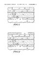
- FIG. 1includes an illustration of a cross-sectional view of a portion of a semiconductor device.
- the semiconductor deviceincludes a semiconductor device substrate 100 , field isolation regions 102 , and doped regions 104 formed within the semiconductor device substrate 100 .
- a gate dielectric layer 106overlies portions of the semiconductor device substrate 100 and a gate electrode 108 overlies the gate dielectric layer 106 .
- a first interlevel dielectric layer (ILD) 110is formed over the gate electrode 108 and the semiconductor device substrate 100 .
- the first interlevel dielectric layer 110is pattered to form dual inlaid openings that are filled with a adhesion/barrier layer 112 and a copper fill material 114 .
- the adhesion/barrier layer 112is typically a refractory metal, a refractory metal nitride, or a combination of refractory metals or their nitrides.
- the copper fill material 114is typically copper or a copper alloy, wherein the copper content is at least 90 atomic percent.
- the coppercan be alloyed with magnesium, sulfur, carbon, or the like to improve adhesion, electromigration, or other properties of the interconnect.
- an insulating barrier layer 122is formed over the copper filled interconnect and first ILD layer 110 .
- This insulating barrier layer 122includes silicon nitride, silicon oxynitride or the like. Using an insulating material to form the insulating barrier layer 122 eliminates the need to form additional patterning and etch processes that would otherwise be required to electrically isolate the interconnects from one another if a conductive barrier would be used.
- a second ILD layer 124is formed over the insulating barrier layer 122 .
- a dual inlaid interconnectcomprising a conductive adhesion/barrier layer 126 and a copper fill material 128 is formed within the second ILD 124 . The dual inlaid interconnect is formed using processes and materials similar to those used to form the dual inlaid interconnect structure in the first ILD layer 110 .
- a passivation layer 22is then formed over the second ILD layer 124 and the dual inlaid interconnect, as shown in FIG. 2.
- the passivation layercan include one or more films of silicon nitride, silicon oxynitride, silicon dioxide, or the like. Portions of the passivation layer 22 closest to the copper fill material 128 typically include silicon nitride or a silicon oxynitride film having a higher concentration of atomic nitrogen relative to atomic oxygen.
- the passivation layer 22is patterned to form a bond pad opening 24 that extends through the passivation layer to the copper fill material 128 .
- a conductive barrier layer 32is deposited over the passivation layer 22 and the copper fill material 128 , as shown in FIG. 3.
- the conductive barrier layer 32can be deposited using processes that can include chemical vapor deposition, physical vapor deposition, evaporation deposition, electroplating, electroless plating, or the like. The thickness of this layer is generally in a range of approximately 50 to 300 nanometers (nm).
- the conductive barrier layer 32includes a refractory metal, a refractory metal nitride, or a combination thereof.
- the conductive barrier layer 32includes a combination of titanium (Ti) and titanium nitride (TiN).
- the titanium/titanium nitride stackimproves adhesion to the underlying copper fill material 128 and passivation layer 22 . Additionally, the titanium nitride forms a barrier that prevents the copper fill material from reacting with subsequently deposited conductive bumps.
- the conductive barrier layer 32can include other materials such as tantalum (Ta), tantalum nitride (TaN), tungsten (W), titanium tungsten nitride (TiWN), titanium tungsten (TiW), tungsten nitride (WN), molybdenum nitride (MoN), cobalt nitride (CoN), or a combination of thereof.
- oxygen tolerant materialscan be used.
- These materialscan include platinum (Pt), palladium (Pd), nickel (Ni), conductive metal oxides or their corresponding metals, or the like.
- the conductive metal oxides and their corresponding metalscan further include iridium (Ir) and iridium oxide (IrO 2 ); ruthenium (Ru) and ruthenium oxide (RuO 2 ); rhenium (Re) and rhenium oxide (ReO 2 and ReO 3 ) or osmium (Os) and osmium oxide (OsO 2 ).
- a resist layer 34is then formed over the conductive barrier layer 32 .
- the resist layer 34exposes portions of the conductive barrier layer 32 overlying the passivation layer 22 .
- the resistis formed such that it covers the bond pad opening 34 .
- itcan also be patterned to extend slightly over surface portions of the conductive barrier layer 32 lying above passivation layer 22 , as shown in FIG. 3.
- the conductive barrier layer 32is then etched, using conventional etching processes, to remove the exposed portions of the conductive barrier layer 32 overlying passivation layer 22 .
- the patterned resist layer 34is removed using a plasma ashing process or, alternatively, using a wet chemical process that uses organic chemicals, such as N-methyl-2-pyrrolidone, acetone, methyl isobutyl ketone (MIBK) or the like.
- the conductive barrier layercan be plated directly over the exposed portions of the copper fill material 128 after forming opening 24 . If so desired, plating can proceed to the extent where the plated material overlies a portion of the passivation layer to form the conductive barrier layer 32 , as shown in FIG. 4.
- a die coat layer 52is then formed over the semiconductor device and patterned to form a die coat opening 54 overlying the bond pad opening 24 , as shown in FIG. 5.
- the peripheral portion of the conductive barrier layer 32have edges that are exposed within the die coat opening 54 .
- the die coat layer 52can be formed as a photo-imagable polyimide film or, alternatively, as a polyimide film that is patterned using conventional resist and etch processing.
- RF sputter cleanPrior to forming a pad limiting metal layer 62 , as shown in FIG. 6, exposed portions of the conductive barrier layer 32 are processed through a radio frequency (RF) sputter clean.
- the RF sputter cleanimproves contact resistance between the barrier layer and the pad limiting metal layer 62 by removing uppermost portions of the conductive barrier layer 32 that can contain impurities, such as oxygen, carbon, fluorine, and chlorine.
- the RF sputter clean processis performed as part of an in-situ process prior to depositing the pad limiting metal (underbump) layer.
- the processing parameters for performing the RF sputter cleanare as follows: RF power is in a range of approximately 1200 to 1500 Watts (W), direct current (DC) bias voltage is in a range of approximately ⁇ 300 to ⁇ 600 volts (V), pressure is in a range of approximately 0.1 to 0.5 Pascals, and time is in a range of approximately 150 to 250 seconds.
- the RF sputter clean processremoves approximately 20-40 nm of barrier material from the surface of the barrier layer 32 .
- the pad limiting metal layer 62is then formed within the die coat opening 54 as illustrated in FIG. 6.
- a Pad limiting metal layertypically includes a functional combination of films that can include an adhesion film, an intermediate coupling/solderable film and an antioxidation barrier film.
- the pad limiting metal layer 62includes a composite of four different films: a chromium film 622 , a chromium-copper alloy film 624 , a copper film 626 , and a gold film 628 .
- the chromium film 622 and the chromium-copper alloy film 624each have a thickness in a range of approximately 50 to 500 nm, the copper film 626 has a thickness in a range of approximately 700 to 1300 nm, and the gold film 628 has a thickness in a range of 80 to 140 nm.
- the pad limiting metalcan include other combinations of films such as a composite of titanium, copper and gold or a composite of titanium, nickel, copper and gold.
- the pad limiting metal layer 62is typically formed by evaporation using a shadow mask. However, other methods, such as sputtering can alternatively be used to form the pad limiting metal.
- a bump materialsuch as a lead tin solder material 72 is deposited over the pad limiting metal layer 62 as shown in FIG. 7.
- the lead tin solder material 72can be evaporated using a shadow mask or, alternatively, it can be formed using other conventional methods, such as plating or solderjetting.
- a reflow processing stepis then performed to round the corners of the lead tin solder material 72 and form the bump as shown in FIG. 7.
- a substantially completed semiconductor devicehas been made.
- This devicecan subsequently be attached to a packaging substrate such as a flip chip or ball grid array package.
- a packaging substratesuch as a flip chip or ball grid array package.
- other levels of interconnectscan be formed as needed.
- other interconnectscan also be made to the gate electrode 108 and the doped region 104 . If additional interconnects would be formed, they would be formed using processes similar to those used to form and deposit insulator barrier layer 122 , second ILD layer 124 , adhesion/barrier layer 126 , and copper fill material 128 .
- FIGS. 8 - 12illustrate an alternative embodiment of the present invention.
- a conductive barrier layer 82is formed over the second ILD layer 124 and copper fill material 128 .
- the conductive barrier layer 82is formed by any of the methods or materials described in forming the conductive barrier layer 32 as first shown in FIG. 3.
- the thickness of the conductive barrier layer 82is typically in a range of approximately 50 to 300 nm.
- an optional oxidation-resistant layer 84is then formed over the conductive barrier layer 82 .
- the oxidation-resistant layercan include any material that either prevents oxidation of the underlying layer or is more readily oxidized in preference to the underlying layer.
- the oxidation-resistant layer 84has a thickness in a range of approximately 10-50 nm.
- a resist layer 86is then formed over the conductive barrier layer 82 and the oxidation-resistant layer 84 .
- the resist layer 86is patterned to cover portions of the conductive barrier layer 82 and the oxidation-resistant layer 84 overlying the copper fill material 128 and the adhesion/barrier layer 126 .
- the unpatterned portions of conductive barrier layer 82 and oxidation-resistant layer 84are then removed using conventional etching processes.
- the resistis then removed, and a passivation layer 92 is formed over the stack comprising conductive barrier layer 82 and oxidation-resistant layer 84 , and portions of the dielectric layer 124 as shown in FIG. 9.
- the passivation layer 92is similar to the passivation layer 22 , first introduced in FIG. 2.
- the passivation layer 92is patterned to form a bond pad opening 94 . As illustrated in FIG. 9, not all of the passivation layer within the bond pad opening is removed. Therefore, the bond pad opening is only partially formed during the patterning process. A residual portion 96 is left to remain over the oxidation-resistant layer 84 after patterning in complete.
- a die coat layer 1001is then formed and patterned to form a die coat opening 1003 , as shown in FIG. 10.
- the die coat layer 1001is similar to the die coat 52 , as first introduced in FIG. 5.
- the die coat opening 1003exposes portions of the passivation layer 92 , including the residual portion 96 .
- an etchis performed to remove the residual portion 96 and the underlying oxidation-resistant layer 84 . This forms the die coat opening 1103 , as shown in FIG. 11. During this etch, portions of the passivation layer 92 exposed by the die coat layer 1001 are also etched, as indicated by the removed passivation layer portions 1102 .
- the passivation layer 92includes silicon and nitrogen, such as silicon nitride or silicon oxynitride, and the oxidation-resistant layer 84 includes silicon nitride. Therefore, the same or similar etch chemistries can be used to remove the residual portions 96 of the passivation layer 92 and the oxidation-resistant layer 84 .
- a pad limiting metal layer 1220is formed similar to the one previously described and includes the chromium film 1222 , the chromium-copper alloy film 1224 , copper film 1226 , and gold film 1228 , and the lead tin solder 1230 .
- an RF sputter cleaning processsimilar to that described previously, can be used to prepare the surface of the barrier layer prior to forming the pad limiting metal layer 1220 .
- a reflow stepis performed to round the shape of the lead tin solder, giving it a dome-like appearance, as shown in FIG. 12.
- the insulating barrier layer 122is used for all interconnect levels except for the uppermost interconnect level.
- the uppermost interconnect levelis the interconnect level over which the bond pads are formed. Therefore, it is the only interconnect level that uses the conductive barrier layer 82 .
- the conductive barrier layer 32can also include an overlying oxidation-resistant layer similar to the oxidation-resistant layer 84 described in the second set of embodiments in FIGS. 8 - 12 .
- the second set of embodimentsdo not necessarily require the use of the oxidation-resistant layer 84 because the residual portion 96 of the passivation layer 92 allows an oxygen-containing plasma to be used without damaging the conductive barrier layer 82 .
- Thiscan be important when the conductive barrier layers 82 or 32 include tantalum nitride, titanium nitride, or the like, which can adversely react with oxygen-containing plasmas or other chemicals used to remove or develop resist or polyimide. Examples of these chemicals can include tetramethyl ammonium hydroxide, N-methyl-2-pyrrolidone, acetone, MIBK, and the like.
- the conductive barrier materialcan also be used to form focused energy-alterable, or laser-alterable, connections between conductive regions of the semiconductor device.
- the conductivity of these connectionscan be modified, using the laser, to program or adjust the circuitry of the device.
- the conductive barrier layeris typically much thinner, less thermally conductive, and less reflective than the interconnect layer, which is normally used to form the laser-alterable connection.
- the conductive barrier layeris also self-passivating as compared to the interconnect layer. Therefore, reliability of the laser alteration is generally improved because the potential for shorting after laser alteration is reduced.
- the laser-alterable connectionis formed closer to uppermost surface of the semiconductor device. This allows the laser to use less power to affect the conductivity of the laser-alterable connection, which correspondingly reduces the potential of causing shorts, damaging adjacent connections, and damaging the surrounding passivation layer.
- the conductive barrier layer and the laser-alterable connectionscan be formed simultaneously using the same layer. Therefore, the process integration requires no additional processing steps.
- the conductive barrier layercan be incorporated as part of the pad limiting metal layer. In this case, it can be evaporated or sputtered onto the wafer before forming the other respective pad limiting metal layer films.
- the pad limiting metal layer and the solder materialcan collectively be formed by physical vapor deposition or by jet printing, whereby individual molten solder drops are deposited into place by an orifice.
- the embodiments described hereincan be integrated into an existing process flow without a need to use exotic materials, develop new processes, or purchase new processing equipment.
- the conductive barrier layers 32 and 82are sufficient to prevent the copper from the interconnect and the lead tin solder from the bump from reacting with each other. Therefore, integrity is maintained at the interface between the bump and the interconnect. This improves the mechanical integrity of the bump as well as helps to reduce the electrical resistance between the bump and the interconnect.
Landscapes
- Engineering & Computer Science (AREA)
- Computer Hardware Design (AREA)
- Microelectronics & Electronic Packaging (AREA)
- Power Engineering (AREA)
- Physics & Mathematics (AREA)
- Condensed Matter Physics & Semiconductors (AREA)
- General Physics & Mathematics (AREA)
- Manufacturing & Machinery (AREA)
- Internal Circuitry In Semiconductor Integrated Circuit Devices (AREA)
Abstract
Description
- This invention relates in general to processes for forming semiconductor devices, and more particularly to processes for forming semiconductor devices including interconnect barrier layers.[0001]
- Forming conductive bumps over semiconductor device bond pads is becoming increasingly common as the sizes and packages of the semiconductor devices continue to shrink. The bumps are used instead of wires to electrically connect the bond pads to their respective packaging leads. One specific type of bump includes a controlled-collapse chip-connection (C[0002]4) bump. Bumps generally require that a pad limiting metal layer be formed between the bond pad and the bump. Pad limiting metal layers typically include chrome and chromium alloys. However, these chromium-containing films can have defects, such as cracks and irregular grain boundaries, which limit the ability of the chromium layer to adequately separate the bond pad and the bump materials.
- The bump typically includes elements such as tin (Sn) and lead (Pb). In the event the barrier fails to keep the bond pad and the bump separated, material from the bond pad can react with the lead or tin in the bump and intermetallic alloys of these materials can be formed. If the bond pad includes a copper-containing material, a brittle intermetallic alloy can be the result. The brittle intermetallic alloy can subsequently crack and result in bump failure. In addition, voids can form as a result of the alloying process and degrade adhesion between the bond pad and the bump. In extreme cases this can produce high resistance that can negatively impact the semiconductor device's performance and even result in failure of the semiconductor device.[0003]
- The present invention is illustrated by way of example and not limitation in the accompanying figures, in which like references indicate similar elements, and in which:[0004]
- FIGS.[0005]1-7 include illustrations of cross-sectional views of forming a semiconductor device having copper interconnects and bumps in accordance with a first set of embodiments.
- FIGS.[0006]8-12 include illustrations of cross-sectional views of forming a semiconductor device having copper interconnects and bumps in accordance with a second set of embodiments.
- Skilled artisans appreciate that elements in the figures are illustrated for simplicity and clarity and have not necessarily been drawn to scale. For example, the dimensions of some of the elements in the figures may be exaggerated relative to other elements to help to improve understanding of embodiments of the present invention.[0007]
- In accordance with embodiments of the present invention a semiconductor device and its method of formation are disclosed. In one embodiment, a conductive barrier layer overlies an interconnect, a passivation layer overlies the conductive barrier layer, and the passivation layer has an opening that exposes portions of the conductive barrier layer. In an alternate embodiment, a passivation layer overlies the interconnect, the passivation layer has an opening that exposes the interconnect, and a conductive barrier layer overlies the interconnect within the opening.[0008]
- FIG. 1 includes an illustration of a cross-sectional view of a portion of a semiconductor device. The semiconductor device includes a[0009]
semiconductor device substrate 100,field isolation regions 102, and dopedregions 104 formed within thesemiconductor device substrate 100. A gatedielectric layer 106 overlies portions of thesemiconductor device substrate 100 and agate electrode 108 overlies the gatedielectric layer 106. - A first interlevel dielectric layer (ILD)[0010]110 is formed over the
gate electrode 108 and thesemiconductor device substrate 100. The first interleveldielectric layer 110 is pattered to form dual inlaid openings that are filled with a adhesion/barrier layer 112 and acopper fill material 114. The adhesion/barrier layer 112 is typically a refractory metal, a refractory metal nitride, or a combination of refractory metals or their nitrides. Thecopper fill material 114 is typically copper or a copper alloy, wherein the copper content is at least 90 atomic percent. The copper can be alloyed with magnesium, sulfur, carbon, or the like to improve adhesion, electromigration, or other properties of the interconnect. After depositing the adhesion/barrier layer 112 and thecopper fill material 114, the substrate is polished to remove portions of the adhesion/barrier layer 112 andcopper fill material 114 outside of the opening. - After forming the first interconnect level, an[0011]
insulating barrier layer 122 is formed over the copper filled interconnect andfirst ILD layer 110. Thisinsulating barrier layer 122 includes silicon nitride, silicon oxynitride or the like. Using an insulating material to form theinsulating barrier layer 122 eliminates the need to form additional patterning and etch processes that would otherwise be required to electrically isolate the interconnects from one another if a conductive barrier would be used. Asecond ILD layer 124 is formed over theinsulating barrier layer 122. A dual inlaid interconnect comprising a conductive adhesion/barrier layer 126 and acopper fill material 128 is formed within thesecond ILD 124. The dual inlaid interconnect is formed using processes and materials similar to those used to form the dual inlaid interconnect structure in thefirst ILD layer 110. - A[0012]
passivation layer 22 is then formed over thesecond ILD layer 124 and the dual inlaid interconnect, as shown in FIG. 2. The passivation layer can include one or more films of silicon nitride, silicon oxynitride, silicon dioxide, or the like. Portions of thepassivation layer 22 closest to thecopper fill material 128 typically include silicon nitride or a silicon oxynitride film having a higher concentration of atomic nitrogen relative to atomic oxygen. Thepassivation layer 22 is patterned to form a bond pad opening24 that extends through the passivation layer to thecopper fill material 128. - A[0013]
conductive barrier layer 32 is deposited over thepassivation layer 22 and thecopper fill material 128, as shown in FIG. 3. Theconductive barrier layer 32 can be deposited using processes that can include chemical vapor deposition, physical vapor deposition, evaporation deposition, electroplating, electroless plating, or the like. The thickness of this layer is generally in a range of approximately 50 to 300 nanometers (nm). Typically, theconductive barrier layer 32 includes a refractory metal, a refractory metal nitride, or a combination thereof. In one embodiment theconductive barrier layer 32 includes a combination of titanium (Ti) and titanium nitride (TiN). The titanium/titanium nitride stack improves adhesion to the underlyingcopper fill material 128 andpassivation layer 22. Additionally, the titanium nitride forms a barrier that prevents the copper fill material from reacting with subsequently deposited conductive bumps. Alternatively, theconductive barrier layer 32 can include other materials such as tantalum (Ta), tantalum nitride (TaN), tungsten (W), titanium tungsten nitride (TiWN), titanium tungsten (TiW), tungsten nitride (WN), molybdenum nitride (MoN), cobalt nitride (CoN), or a combination of thereof. In other embodiments, oxygen tolerant materials can be used. These materials can include platinum (Pt), palladium (Pd), nickel (Ni), conductive metal oxides or their corresponding metals, or the like. The conductive metal oxides and their corresponding metals can further include iridium (Ir) and iridium oxide (IrO2); ruthenium (Ru) and ruthenium oxide (RuO2); rhenium (Re) and rhenium oxide (ReO2and ReO3) or osmium (Os) and osmium oxide (OsO2). - A[0014]
resist layer 34 is then formed over theconductive barrier layer 32. Theresist layer 34 exposes portions of theconductive barrier layer 32 overlying thepassivation layer 22. The resist is formed such that it covers the bond pad opening34. In addition, it can also be patterned to extend slightly over surface portions of theconductive barrier layer 32 lying abovepassivation layer 22, as shown in FIG. 3. - The[0015]
conductive barrier layer 32 is then etched, using conventional etching processes, to remove the exposed portions of theconductive barrier layer 32 overlyingpassivation layer 22. After the etch, the patternedresist layer 34 is removed using a plasma ashing process or, alternatively, using a wet chemical process that uses organic chemicals, such as N-methyl-2-pyrrolidone, acetone, methyl isobutyl ketone (MIBK) or the like. - Alternatively, if a plating process such as electroplating or electroless plating is used to form the conductive barrier layer, the previously described patterning process may not be necessary. Instead, the conductive barrier layer can be plated directly over the exposed portions of the[0016]
copper fill material 128 after formingopening 24. If so desired, plating can proceed to the extent where the plated material overlies a portion of the passivation layer to form theconductive barrier layer 32, as shown in FIG. 4. - A[0017]
die coat layer 52 is then formed over the semiconductor device and patterned to form adie coat opening 54 overlying the bond pad opening24, as shown in FIG. 5. In this specific embodiment, the peripheral portion of theconductive barrier layer 32 have edges that are exposed within thedie coat opening 54. Thedie coat layer 52 can be formed as a photo-imagable polyimide film or, alternatively, as a polyimide film that is patterned using conventional resist and etch processing. - Prior to forming a pad limiting[0018]
metal layer 62, as shown in FIG. 6, exposed portions of theconductive barrier layer 32 are processed through a radio frequency (RF) sputter clean. The RF sputter clean improves contact resistance between the barrier layer and the pad limitingmetal layer 62 by removing uppermost portions of theconductive barrier layer 32 that can contain impurities, such as oxygen, carbon, fluorine, and chlorine. In one embodiment, the RF sputter clean process is performed as part of an in-situ process prior to depositing the pad limiting metal (underbump) layer. In one embodiment, the processing parameters for performing the RF sputter clean are as follows: RF power is in a range of approximately 1200 to 1500 Watts (W), direct current (DC) bias voltage is in a range of approximately −300 to −600 volts (V), pressure is in a range of approximately 0.1 to 0.5 Pascals, and time is in a range of approximately 150 to 250 seconds. The RF sputter clean process removes approximately 20-40 nm of barrier material from the surface of thebarrier layer 32. - The pad limiting[0019]
metal layer 62 is then formed within thedie coat opening 54 as illustrated in FIG. 6. A Pad limiting metal layer typically includes a functional combination of films that can include an adhesion film, an intermediate coupling/solderable film and an antioxidation barrier film. In one embodiment, the pad limitingmetal layer 62 includes a composite of four different films: achromium film 622, a chromium-copper alloy film 624, acopper film 626, and agold film 628. Thechromium film 622 and the chromium-copper alloy film 624 each have a thickness in a range of approximately 50 to 500 nm, thecopper film 626 has a thickness in a range of approximately 700 to 1300 nm, and thegold film 628 has a thickness in a range of 80 to 140 nm. Alternatively, the pad limiting metal can include other combinations of films such as a composite of titanium, copper and gold or a composite of titanium, nickel, copper and gold. The pad limitingmetal layer 62 is typically formed by evaporation using a shadow mask. However, other methods, such as sputtering can alternatively be used to form the pad limiting metal. - In accordance with one embodiment, following the formation of pad limiting metal layer, a bump material, such as a lead[0020]
tin solder material 72 is deposited over the pad limitingmetal layer 62 as shown in FIG. 7. The leadtin solder material 72 can be evaporated using a shadow mask or, alternatively, it can be formed using other conventional methods, such as plating or solderjetting. A reflow processing step is then performed to round the corners of the leadtin solder material 72 and form the bump as shown in FIG. 7. - At this point in the process, a substantially completed semiconductor device has been made. This device can subsequently be attached to a packaging substrate such as a flip chip or ball grid array package. Although not shown, other levels of interconnects can be formed as needed. Similarly, other interconnects can also be made to the[0021]
gate electrode 108 and the dopedregion 104. If additional interconnects would be formed, they would be formed using processes similar to those used to form and depositinsulator barrier layer 122,second ILD layer 124, adhesion/barrier layer 126, andcopper fill material 128. - FIGS.[0022]8-12 illustrate an alternative embodiment of the present invention. Referring to FIG. 8, a
conductive barrier layer 82 is formed over thesecond ILD layer 124 andcopper fill material 128. Theconductive barrier layer 82 is formed by any of the methods or materials described in forming theconductive barrier layer 32 as first shown in FIG. 3. The thickness of theconductive barrier layer 82 is typically in a range of approximately 50 to 300 nm. In this particular embodiment, an optional oxidation-resistant layer 84 is then formed over theconductive barrier layer 82. The oxidation-resistant layer can include any material that either prevents oxidation of the underlying layer or is more readily oxidized in preference to the underlying layer. Examples of materials that can be used include silicon nitride, polysilicon, amorphous silicon, or a conductive metal oxide or its corresponding conductive metal. The oxidation-resistant layer 84 has a thickness in a range of approximately 10-50 nm. A resistlayer 86 is then formed over theconductive barrier layer 82 and the oxidation-resistant layer 84. The resistlayer 86 is patterned to cover portions of theconductive barrier layer 82 and the oxidation-resistant layer 84 overlying thecopper fill material 128 and the adhesion/barrier layer 126. - The unpatterned portions of[0023]
conductive barrier layer 82 and oxidation-resistant layer 84 are then removed using conventional etching processes. The resist is then removed, and apassivation layer 92 is formed over the stack comprisingconductive barrier layer 82 and oxidation-resistant layer 84, and portions of thedielectric layer 124 as shown in FIG. 9. Thepassivation layer 92 is similar to thepassivation layer 22, first introduced in FIG. 2. In this particular embodiment, thepassivation layer 92 is patterned to form abond pad opening 94. As illustrated in FIG. 9, not all of the passivation layer within the bond pad opening is removed. Therefore, the bond pad opening is only partially formed during the patterning process. Aresidual portion 96 is left to remain over the oxidation-resistant layer 84 after patterning in complete. - A[0024]
die coat layer 1001 is then formed and patterned to form adie coat opening 1003, as shown in FIG. 10. Thedie coat layer 1001 is similar to thedie coat 52, as first introduced in FIG. 5. Thedie coat opening 1003 exposes portions of thepassivation layer 92, including theresidual portion 96. After forming thedie coat opening 1003, an etch is performed to remove theresidual portion 96 and the underlying oxidation-resistant layer 84. This forms the die coat opening1103, as shown in FIG. 11. During this etch, portions of thepassivation layer 92 exposed by thedie coat layer 1001 are also etched, as indicated by the removedpassivation layer portions 1102. In one particular embodiment, thepassivation layer 92 includes silicon and nitrogen, such as silicon nitride or silicon oxynitride, and the oxidation-resistant layer 84 includes silicon nitride. Therefore, the same or similar etch chemistries can be used to remove theresidual portions 96 of thepassivation layer 92 and the oxidation-resistant layer 84. - Processing is continued to form a substantially completed device as shown in FIG. 12. A pad limiting[0025]
metal layer 1220 is formed similar to the one previously described and includes thechromium film 1222, the chromium-copper alloy film 1224,copper film 1226, andgold film 1228, and thelead tin solder 1230. If necessary, an RF sputter cleaning process, similar to that described previously, can be used to prepare the surface of the barrier layer prior to forming the pad limitingmetal layer 1220. In this particular embodiment, a reflow step is performed to round the shape of the lead tin solder, giving it a dome-like appearance, as shown in FIG. 12. - In the embodiments described in FIGS.[0026]9-12, the insulating
barrier layer 122 is used for all interconnect levels except for the uppermost interconnect level. The uppermost interconnect level is the interconnect level over which the bond pads are formed. Therefore, it is the only interconnect level that uses theconductive barrier layer 82. - There are many other embodiments that are possible with the present invention. Turning to FIG. 3, the[0027]
conductive barrier layer 32 can also include an overlying oxidation-resistant layer similar to the oxidation-resistant layer 84 described in the second set of embodiments in FIGS.8-12. Similarly, the second set of embodiments do not necessarily require the use of the oxidation-resistant layer 84 because theresidual portion 96 of thepassivation layer 92 allows an oxygen-containing plasma to be used without damaging theconductive barrier layer 82. This can be important when the conductive barrier layers82 or32 include tantalum nitride, titanium nitride, or the like, which can adversely react with oxygen-containing plasmas or other chemicals used to remove or develop resist or polyimide. Examples of these chemicals can include tetramethyl ammonium hydroxide, N-methyl-2-pyrrolidone, acetone, MIBK, and the like. - In addition to forming the conductive barrier layer over the bond pad as described in FIGS.[0028]9-12, the conductive barrier material can also be used to form focused energy-alterable, or laser-alterable, connections between conductive regions of the semiconductor device. The conductivity of these connections can be modified, using the laser, to program or adjust the circuitry of the device.
- Forming the laser-alterable connections using the conductive barrier layer has advantages over the prior art. The conductive barrier layer is typically much thinner, less thermally conductive, and less reflective than the interconnect layer, which is normally used to form the laser-alterable connection. The conductive barrier layer is also self-passivating as compared to the interconnect layer. Therefore, reliability of the laser alteration is generally improved because the potential for shorting after laser alteration is reduced. In addition the laser-alterable connection is formed closer to uppermost surface of the semiconductor device. This allows the laser to use less power to affect the conductivity of the laser-alterable connection, which correspondingly reduces the potential of causing shorts, damaging adjacent connections, and damaging the surrounding passivation layer. Furthermore, the conductive barrier layer and the laser-alterable connections can be formed simultaneously using the same layer. Therefore, the process integration requires no additional processing steps.[0029]
- Although specific materials were listed with respect to the pad limiting[0030]
metal layer 62, other materials and other variations of this integration scheme can alternatively be used. For example, the conductive barrier layer can be incorporated as part of the pad limiting metal layer. In this case, it can be evaporated or sputtered onto the wafer before forming the other respective pad limiting metal layer films. In yet another embodiment, the pad limiting metal layer and the solder material can collectively be formed by physical vapor deposition or by jet printing, whereby individual molten solder drops are deposited into place by an orifice. - The embodiments described herein can be integrated into an existing process flow without a need to use exotic materials, develop new processes, or purchase new processing equipment. The conductive barrier layers[0031]32 and82 are sufficient to prevent the copper from the interconnect and the lead tin solder from the bump from reacting with each other. Therefore, integrity is maintained at the interface between the bump and the interconnect. This improves the mechanical integrity of the bump as well as helps to reduce the electrical resistance between the bump and the interconnect.
- In the foregoing specification, the invention has been described with reference to specific embodiments. However, one of ordinary skill in the art appreciates that various modifications and changes can be made without departing from the scope of the present invention as set forth in the claims below. Accordingly, the specification and figures are to be regarded in an illustrative rather than a restrictive sense, and all such modifications are intended to be included within the scope of present invention. Benefits, other advantages, and solutions to problems have been described with regard to specific embodiments. However, the benefits, advantages, solutions to problems, and any element(s) that may cause any benefit, advantage, or solution to occur or become more pronounced are not to be construed as a critical, required, or essential feature or element of any or all the claims.[0032]
Claims (31)
1. A semiconductor device, comprising:
a first interconnect that overlies a semiconductor device substrate;
a insulating barrier layer that overlies the first interconnect;
a second interconnect that overlies portions of the first interconnect and the insulating barrier layer;
a conductive barrier layer that overlies a portion the second interconnect, the conductive barrier layer extending beyond an edge region of the portion of the second interconnect; and
a passivation layer that overlies the conductive barrier layer, the passivation layer having an opening that exposes portions of the conductive barrier layer.
2. The semiconductor device ofclaim 1 , wherein the second interconnect includes mostly copper.
3. The semiconductor device ofclaim 1 , wherein the conductive barrier layer includes a refractory metal nitride.
4. The semiconductor device ofclaim 1 , wherein the conductive barrier layer includes a material selected from a group consisting of titanium, tantalum, tungsten, iridium, and nickel.
5. The semiconductor device ofclaim 1 , further comprising an oxidation-resistant layer that overlies the conductive barrier layer.
6. The semiconductor device ofclaim 5 , wherein the oxidation-resistant layer includes nitrogen.
7. The semiconductor device ofclaim 5 , wherein the oxidation-resistant layer is a silicon layer.
8. The semiconductor device ofclaim 1 , wherein the portion of the second interconnect is further characterized as a bond pad.
9. The semiconductor device ofclaim 8 , wherein a portion of the conductive barrier layer is a laser-alterable connection between at least two conductive regions.
10. The semiconductor device ofclaim 8 , further comprising
a conductive bump that overlies the bond pad.
11. A semiconductor device, comprising:
an interconnect over a semiconductor device substrate;
a passivation layer that overlies the interconnect, the passivation layer having an opening that exposes a portion of the interconnect; and
a conductive barrier layer within the opening that overlies the portion of the interconnect.
12. The semiconductor device ofclaim 11 , wherein the conductive barrier layer covers a sidewall portion of the opening.
13. The semiconductor device ofclaim 12 , wherein the conductive barrier layer extends over a surface portion of the passivation layer adjacent the sidewall portion.
14. The semiconductor device ofclaim 11 , wherein the interconnect includes mostly copper.
15. The semiconductor device ofclaim 11 , wherein the conductive barrier layer includes a refractory metal nitride.
16. The semiconductor device ofclaim 11 , wherein the conductive barrier layer includes a material selected from a group consisting of tantalum, titanium, tungsten, iridium, and nickel.
17. The semiconductor device ofclaim 11 , further comprising forming an oxidation-resistant layer over the conductive barrier layer.
18. The semiconductor device ofclaim 17 , wherein the oxidation-resistant layer includes nitrogen.
19. The semiconductor device ofclaim 17 , wherein the oxidation-resistant layer is a silicon layer.
20. The semiconductor device ofclaim 11 , further comprising a conductive bump over the conductive barrier layer.
21. A method of forming a semiconductor device comprising:
forming a first interconnect overlying a semiconductor device substrate;
forming an insulating barrier layer overlying the first interconnect;
forming a second interconnect overlying portions of the first interconnect and the insulating barrier layer;
forming a conductive barrier layer overlying a portion of the second interconnect, the conductive barrier layer extending beyond an edge region of the portion of the second interconnect;
forming a passivation layer overlying the conductive barrier layer; and
forming an opening in the passivation layer, wherein the opening exposes portions of the conductive barrier layer.
22. The method ofclaim 21 , further comprising forming an oxidation-resistant layer overlying conductive barrier layer.
23. The method ofclaim 22 , wherein the oxidation-resistant layer includes a material selected from a group consisting of nitrogen and silicon.
24. The method ofclaim 21 , wherein a portion of the conductive barrier layer forms a laser-alterable connection between at least two conductive regions.
25. The method ofclaim 21 , wherein forming an opening in the passivation layer further comprises:
forming a partial opening in the passivation layer, wherein a depth of the partial opening is less than a thickness of the passivation layer in a region of the passivation layer where the partial opening is formed;
forming a die coat layer over the passivation layer;
forming an opening in the die coat layer, wherein forming the opening in the die coat layer exposes the partial opening in the passivation layer; and
etching the partial opening in the passivation layer to expose an underlying layer after forming an opening in the die coat layer.
26. The method ofclaim 21 , further comprising:
removing a portion of the conductive barrier layer after forming an opening in the passivation layer, wherein the portion of the conductive barrier layer has a depth; and
forming a conductive bump over the conductive barrier layer after removing a portion of the conductive barrier layer.
27. The method ofclaim 26 , wherein the depth is in a range of approximately 20-40 nanometers.
28. A method of forming a semiconductor device, comprising:
forming an interconnect over a semiconductor device substrate;
forming a passivation layer over the interconnect;
forming an opening in the passivation layer, the opening exposing portions of the interconnect; and
forming a conductive barrier layer within the opening, the conductive barrier layer overlying exposed portions of the interconnect.
29. The method ofclaim 28 , further comprising forming an oxidation-resistant layer over the conductive barrier layer, wherein the oxidation-resistant layer includes a material selected from a group consisting of nitrogen and silicon.
30. The method ofclaim 28 , wherein the conductive barrier layer covers a sidewall portion of the opening and extends over a surface portion of the passivation layer adjacent the sidewall portion.
31. The method ofclaim 28 , wherein the interconnect includes copper.
Priority Applications (7)
| Application Number | Priority Date | Filing Date | Title |
|---|---|---|---|
| US09/285,666US20020000665A1 (en) | 1999-04-05 | 1999-04-05 | Semiconductor device conductive bump and interconnect barrier |
| JP2000086214AJP4566325B2 (en) | 1999-04-05 | 2000-03-27 | Method for manufacturing a semiconductor device |
| TW089106143ATW490793B (en) | 1999-04-05 | 2000-04-01 | Semiconductor device and method of formation |
| SG200001904ASG84587A1 (en) | 1999-04-05 | 2000-04-04 | Semiconductor device and method of formation |
| CNB001049275ACN1192430C (en) | 1999-04-05 | 2000-04-04 | Semiconductor device and method for manufacturing the same |
| US09/609,523US6500750B1 (en) | 1999-04-05 | 2000-07-03 | Semiconductor device and method of formation |
| US10/051,262US6713381B2 (en) | 1999-04-05 | 2002-01-18 | Method of forming semiconductor device including interconnect barrier layers |
Applications Claiming Priority (1)
| Application Number | Priority Date | Filing Date | Title |
|---|---|---|---|
| US09/285,666US20020000665A1 (en) | 1999-04-05 | 1999-04-05 | Semiconductor device conductive bump and interconnect barrier |
Related Child Applications (2)
| Application Number | Title | Priority Date | Filing Date |
|---|---|---|---|
| US09/609,523ContinuationUS6500750B1 (en) | 1999-04-05 | 2000-07-03 | Semiconductor device and method of formation |
| US10/051,262DivisionUS6713381B2 (en) | 1999-04-05 | 2002-01-18 | Method of forming semiconductor device including interconnect barrier layers |
Publications (1)
| Publication Number | Publication Date |
|---|---|
| US20020000665A1true US20020000665A1 (en) | 2002-01-03 |
Family
ID=23095213
Family Applications (2)
| Application Number | Title | Priority Date | Filing Date |
|---|---|---|---|
| US09/285,666AbandonedUS20020000665A1 (en) | 1999-04-05 | 1999-04-05 | Semiconductor device conductive bump and interconnect barrier |
| US10/051,262Expired - Fee RelatedUS6713381B2 (en) | 1999-04-05 | 2002-01-18 | Method of forming semiconductor device including interconnect barrier layers |
Family Applications After (1)
| Application Number | Title | Priority Date | Filing Date |
|---|---|---|---|
| US10/051,262Expired - Fee RelatedUS6713381B2 (en) | 1999-04-05 | 2002-01-18 | Method of forming semiconductor device including interconnect barrier layers |
Country Status (5)
| Country | Link |
|---|---|
| US (2) | US20020000665A1 (en) |
| JP (1) | JP4566325B2 (en) |
| CN (1) | CN1192430C (en) |
| SG (1) | SG84587A1 (en) |
| TW (1) | TW490793B (en) |
Cited By (60)
| Publication number | Priority date | Publication date | Assignee | Title |
|---|---|---|---|---|
| US20010026952A1 (en)* | 1998-09-23 | 2001-10-04 | Manfred Engelhardt | Integrated circuit configuration and production method |
| US20020015128A1 (en)* | 2000-06-21 | 2002-02-07 | Hirokazu Sakaguchi | LCD driver IC chip |
| US20020066959A1 (en)* | 2000-12-04 | 2002-06-06 | Rajeev Joshi | Passivation scheme for bumped wafers |
| US20020142576A1 (en)* | 1999-08-10 | 2002-10-03 | Hitachi, Ltd. | Semiconductor integrated circuit device and manufacturing method of semiconductor integrated circuit device |
| US6577011B1 (en)* | 1997-07-10 | 2003-06-10 | International Business Machines Corporation | Chip interconnect wiring structure with low dielectric constant insulator and methods for fabricating the same |
| US20030222295A1 (en)* | 1998-12-21 | 2003-12-04 | Megic Corporation | High performance system-on-chip inductor using post passivation process |
| US20040053483A1 (en)* | 2002-06-25 | 2004-03-18 | Nair Krishna K. | Methods of forming electronic structures including conductive shunt layers and related structures |
| US6798050B1 (en)* | 1999-09-22 | 2004-09-28 | Kabushiki Kaisha Toshiba | Semiconductor device having semiconductor element with copper pad mounted on wiring substrate and method for fabricating the same |
| US20040188851A1 (en)* | 2003-03-26 | 2004-09-30 | Nec Electronics Corporation | Semiconductor device and method for manufacturing same |
| US20040209406A1 (en)* | 2003-02-18 | 2004-10-21 | Jong-Rong Jan | Methods of selectively bumping integrated circuit substrates and related structures |
| US20040206801A1 (en)* | 2001-09-27 | 2004-10-21 | Mis J. Daniel | Electronic devices including metallurgy structures for wire and solder bonding |
| US20040224497A1 (en)* | 2003-05-05 | 2004-11-11 | Hans-Joachim Barth | Method to form selective cap layers on metal features with narrow spaces |
| US20050023590A1 (en)* | 2000-12-28 | 2005-02-03 | Jingyu Lian | Multi-layer electrode and method of forming the same |
| US20050082552A1 (en)* | 2003-10-21 | 2005-04-21 | Ming Fang | Large bumps for optical flip chips |
| US20050083592A1 (en)* | 2003-09-10 | 2005-04-21 | Yaakov Amitai | High Brightness optical device |
| US6900545B1 (en)* | 1999-06-25 | 2005-05-31 | International Business Machines Corporation | Variable thickness pads on a substrate surface |
| US20050184358A1 (en)* | 1998-12-21 | 2005-08-25 | Megic Corporation | High performance system-on-chip using post passivation process |
| US20050206067A1 (en)* | 2004-03-18 | 2005-09-22 | Cook William P | Input tray and drive mechanism using a single motor for an image forming device |
| US20050218527A1 (en)* | 2002-07-31 | 2005-10-06 | Fujitsu Limited | Semiconductor device for preventing defective filling of interconnection and cracking of insulating film |
| US20050269697A1 (en)* | 2004-06-04 | 2005-12-08 | Seiko Epson Corporation | Semiconductor device, circuit board, and electronic instrument |
| US20050279809A1 (en)* | 2000-11-10 | 2005-12-22 | Rinne Glenn A | Optical structures including liquid bumps and related methods |
| US20060022343A1 (en)* | 2004-07-29 | 2006-02-02 | Megic Corporation | Very thick metal interconnection scheme in IC chips |
| US20060030139A1 (en)* | 2002-06-25 | 2006-02-09 | Mis J D | Methods of forming lead free solder bumps and related structures |
| US20060076679A1 (en)* | 2002-06-25 | 2006-04-13 | Batchelor William E | Non-circular via holes for bumping pads and related structures |
| US20060205170A1 (en)* | 2005-03-09 | 2006-09-14 | Rinne Glenn A | Methods of forming self-healing metal-insulator-metal (MIM) structures and related devices |
| US20060205204A1 (en)* | 2005-03-14 | 2006-09-14 | Michael Beck | Method of making a semiconductor interconnect with a metal cap |
| US20060289961A1 (en)* | 2005-06-23 | 2006-12-28 | Seiko Epson Corporation | Semiconductor device |
| US7156284B2 (en) | 2000-12-15 | 2007-01-02 | Unitive International Limited | Low temperature methods of bonding components and related structures |
| US20070045855A1 (en)* | 2005-07-22 | 2007-03-01 | Megica Corporation | Method for forming a double embossing structure |
| US7205221B2 (en)* | 1999-09-02 | 2007-04-17 | Micron Technology, Inc. | Under bump metallization pad and solder bump connections |
| US20070182004A1 (en)* | 2006-02-08 | 2007-08-09 | Rinne Glenn A | Methods of Forming Electronic Interconnections Including Compliant Dielectric Layers and Related Devices |
| US20070190776A1 (en)* | 2003-09-09 | 2007-08-16 | Intel Corporation | Methods of Processing Thick ILD Layers Using Spray Coating or Lamination for C4 Wafer Level Thick Metal Integrated Flow |
| US20070262457A1 (en)* | 1998-12-21 | 2007-11-15 | Mou-Shiung Lin | Top layers of metal for high performance IC's |
| US20080001290A1 (en)* | 2006-06-28 | 2008-01-03 | Megica Corporation | Integrated circuit (IC) chip and method for fabricating the same |
| US20080006905A1 (en)* | 2003-01-15 | 2008-01-10 | Infineon Technologies Ag | Method for production of an integrated circuit bar arrangement, in particular comprising a capacitor assembly, as well as an integrated circuit arrangement |
| US20080042280A1 (en)* | 2006-06-28 | 2008-02-21 | Megica Corporation | Semiconductor chip structure |
| US20080099913A1 (en)* | 2006-10-31 | 2008-05-01 | Matthias Lehr | Metallization layer stack without a terminal aluminum metal layer |
| US20080102540A1 (en)* | 2006-10-31 | 2008-05-01 | Tobias Letz | Technique for forming a passivation layer without a terminal metal |
| WO2008054680A3 (en)* | 2006-10-31 | 2008-06-26 | Advanced Micro Devices Inc | A metallization layer stack without a terminal aluminum metal layer |
| US20080284032A1 (en)* | 2005-03-29 | 2008-11-20 | Megica Corporation | High performance system-on-chip using post passivation process |
| US20080284014A1 (en)* | 2007-03-13 | 2008-11-20 | Megica Corporation | Chip assembly |
| DE102007057689A1 (en)* | 2007-11-30 | 2009-06-04 | Advanced Micro Devices, Inc., Sunnyvale | Semiconductor device having a chip area, which is designed for an aluminum-free solder bump connection, and a test structure, which is designed for an aluminum-free wire connection |
| US20090184394A1 (en)* | 1998-12-21 | 2009-07-23 | Megica Corporation | High performance system-on-chip inductor using post passivation process |
| US7674701B2 (en) | 2006-02-08 | 2010-03-09 | Amkor Technology, Inc. | Methods of forming metal layers using multi-layer lift-off patterns |
| US20100283073A1 (en)* | 2007-09-28 | 2010-11-11 | Osram Opto Semiconductors Gmbh | Thin-Film LED Having a Mirror Layer and Method for the Production Thereof |
| US7973629B2 (en) | 2001-09-04 | 2011-07-05 | Megica Corporation | Method for making high-performance RF integrated circuits |
| US8008775B2 (en) | 2004-09-09 | 2011-08-30 | Megica Corporation | Post passivation interconnection structures |
| US8018060B2 (en) | 2004-09-09 | 2011-09-13 | Megica Corporation | Post passivation interconnection process and structures |
| US20110233796A1 (en)* | 2010-03-23 | 2011-09-29 | Kim Deok-Kee | Semiconductor Devices and Electronic Systems |
| DE102011005642A1 (en)* | 2011-03-16 | 2012-09-20 | GLOBALFOUNDRIES Dresden Module One Ltd. Liability Company & Co. KG | A method for protecting reactive metal surfaces of semiconductor devices during transport by providing an additional protective layer |
| US20130029483A1 (en)* | 2008-07-15 | 2013-01-31 | Semiconductor Manufacturing International (Shanghai) Corporation | Method and system for forming conductive bumping with copper interconnection |
| US8878365B2 (en) | 2005-07-13 | 2014-11-04 | Seiko Epson Corporation | Semiconductor device having a conductive layer reliably formed under an electrode pad |
| TWI460820B (en)* | 2006-06-28 | 2014-11-11 | Qualcomm Inc | Integrated circuit (IC) chip and its process |
| US20190304939A1 (en)* | 2018-03-27 | 2019-10-03 | Taiwan Semiconductor Manufacturing Co., Ltd. | Redistribution Layer Metallic Structure and Method |
| US11189538B2 (en)* | 2018-09-28 | 2021-11-30 | Taiwan Semiconductor Manufacturing Co., Ltd. | Semiconductor structure with polyimide packaging and manufacturing method |
| US11367683B2 (en) | 2018-07-03 | 2022-06-21 | Infineon Technologies Ag | Silicon carbide device and method for forming a silicon carbide device |
| US11869840B2 (en) | 2018-07-03 | 2024-01-09 | Infineon Technologies Ag | Silicon carbide device and method for forming a silicon carbide device |
| US20240213092A1 (en)* | 2022-12-22 | 2024-06-27 | International Business Machines Corporation | Octagonal interconnect wiring for advanced logic |
| DE102016114867B4 (en) | 2015-12-31 | 2025-03-13 | Taiwan Semiconductor Manufacturing Company, Ltd. | Semiconductor device, film stack and method for producing the same |
| US12424579B2 (en) | 2021-02-02 | 2025-09-23 | Taiwan Semiconductor Manufacturing Company, Ltd. | Integrated chip including an upper conductive structure having multilayer stack to decrease fabrication costs and increase performance |
Families Citing this family (62)
| Publication number | Priority date | Publication date | Assignee | Title |
|---|---|---|---|---|
| JPH11340265A (en)* | 1998-05-22 | 1999-12-10 | Sony Corp | Semiconductor device and its manufacture |
| US7381642B2 (en)* | 2004-09-23 | 2008-06-03 | Megica Corporation | Top layers of metal for integrated circuits |
| US7405149B1 (en)* | 1998-12-21 | 2008-07-29 | Megica Corporation | Post passivation method for semiconductor chip or wafer |
| US6544880B1 (en)* | 1999-06-14 | 2003-04-08 | Micron Technology, Inc. | Method of improving copper interconnects of semiconductor devices for bonding |
| US7494927B2 (en)* | 2000-05-15 | 2009-02-24 | Asm International N.V. | Method of growing electrical conductors |
| JP2004516682A (en)* | 2000-12-22 | 2004-06-03 | コーニンクレッカ フィリップス エレクトロニクス エヌ ヴィ | Integrated circuit device |
| JP2003045877A (en)* | 2001-08-01 | 2003-02-14 | Sharp Corp | Semiconductor device and method of manufacturing the same |
| US7049226B2 (en)* | 2001-09-26 | 2006-05-23 | Applied Materials, Inc. | Integration of ALD tantalum nitride for copper metallization |
| US6916398B2 (en)* | 2001-10-26 | 2005-07-12 | Applied Materials, Inc. | Gas delivery apparatus and method for atomic layer deposition |
| JP3820975B2 (en)* | 2001-12-12 | 2006-09-13 | ソニー株式会社 | Semiconductor device and manufacturing method thereof |
| US6661098B2 (en)* | 2002-01-18 | 2003-12-09 | International Business Machines Corporation | High density area array solder microjoining interconnect structure and fabrication method |
| JP4340416B2 (en)* | 2002-02-26 | 2009-10-07 | Spansion Japan株式会社 | Manufacturing method of semiconductor memory device |
| JP2004214594A (en)* | 2002-11-15 | 2004-07-29 | Sharp Corp | Semiconductor device and method of manufacturing the same |
| JP4170103B2 (en)* | 2003-01-30 | 2008-10-22 | Necエレクトロニクス株式会社 | Semiconductor device and manufacturing method of semiconductor device |
| US6869878B1 (en)* | 2003-02-14 | 2005-03-22 | Advanced Micro Devices, Inc. | Method of forming a selective barrier layer using a sacrificial layer |
| US7026714B2 (en)* | 2003-03-18 | 2006-04-11 | Cunningham James A | Copper interconnect systems which use conductive, metal-based cap layers |
| US7238610B2 (en)* | 2003-03-31 | 2007-07-03 | Intel Corporation | Method and apparatus for selective deposition |
| US7566964B2 (en)* | 2003-04-10 | 2009-07-28 | Agere Systems Inc. | Aluminum pad power bus and signal routing for integrated circuit devices utilizing copper technology interconnect structures |
| DE10335182B4 (en)* | 2003-07-30 | 2007-03-01 | Infineon Technologies Ag | Arrangement for improving the module reliability |
| DE10337569B4 (en)* | 2003-08-14 | 2008-12-11 | Infineon Technologies Ag | Integrated connection arrangement and manufacturing method |
| US6977435B2 (en)* | 2003-09-09 | 2005-12-20 | Intel Corporation | Thick metal layer integrated process flow to improve power delivery and mechanical buffering |
| US7294565B2 (en)* | 2003-10-01 | 2007-11-13 | International Business Machines Corporation | Method of fabricating a wire bond pad with Ni/Au metallization |
| DE102004048202B4 (en)* | 2004-09-30 | 2008-05-21 | Infineon Technologies Ag | Method for separating surface-mountable semiconductor components and for equipping them with external contacts |
| US7666773B2 (en) | 2005-03-15 | 2010-02-23 | Asm International N.V. | Selective deposition of noble metal thin films |
| US8025922B2 (en)* | 2005-03-15 | 2011-09-27 | Asm International N.V. | Enhanced deposition of noble metals |
| US20070014919A1 (en)* | 2005-07-15 | 2007-01-18 | Jani Hamalainen | Atomic layer deposition of noble metal oxides |
| US7960838B2 (en) | 2005-11-18 | 2011-06-14 | United Microelectronics Corp. | Interconnect structure |
| KR100735526B1 (en)* | 2006-02-08 | 2007-07-04 | 삼성전자주식회사 | Semiconductor devices having improved wire bonding reliability, reticles used in the manufacture thereof, and methods of manufacturing the same |
| US20080038913A1 (en)* | 2006-08-10 | 2008-02-14 | International Business Machines Corporation | Methods of forming aluminum-free wire bond pad and pad so formed |
| US7435484B2 (en)* | 2006-09-01 | 2008-10-14 | Asm Japan K.K. | Ruthenium thin film-formed structure |
| US7682959B2 (en)* | 2007-03-21 | 2010-03-23 | Stats Chippac, Ltd. | Method of forming solder bump on high topography plated Cu |
| US7964934B1 (en) | 2007-05-22 | 2011-06-21 | National Semiconductor Corporation | Fuse target and method of forming the fuse target in a copper process flow |
| US8030733B1 (en) | 2007-05-22 | 2011-10-04 | National Semiconductor Corporation | Copper-compatible fuse target |
| US20090087339A1 (en)* | 2007-09-28 | 2009-04-02 | Asm Japan K.K. | METHOD FOR FORMING RUTHENIUM COMPLEX FILM USING Beta-DIKETONE-COORDINATED RUTHENIUM PRECURSOR |
| KR101544198B1 (en)* | 2007-10-17 | 2015-08-12 | 한국에이에스엠지니텍 주식회사 | Ruthenium film formation method |
| US7829450B2 (en)* | 2007-11-07 | 2010-11-09 | Infineon Technologies Ag | Method of processing a contact pad, method of manufacturing a contact pad, and integrated circuit element |
| KR20090067505A (en)* | 2007-12-21 | 2009-06-25 | 에이에스엠지니텍코리아 주식회사 | Ruthenium film deposition method |
| US8084104B2 (en)* | 2008-08-29 | 2011-12-27 | Asm Japan K.K. | Atomic composition controlled ruthenium alloy film formed by plasma-enhanced atomic layer deposition |
| US7709956B2 (en)* | 2008-09-15 | 2010-05-04 | National Semiconductor Corporation | Copper-topped interconnect structure that has thin and thick copper traces and method of forming the copper-topped interconnect structure |
| US8133555B2 (en) | 2008-10-14 | 2012-03-13 | Asm Japan K.K. | Method for forming metal film by ALD using beta-diketone metal complex |
| US9379011B2 (en) | 2008-12-19 | 2016-06-28 | Asm International N.V. | Methods for depositing nickel films and for making nickel silicide and nickel germanide |
| US20100155949A1 (en)* | 2008-12-24 | 2010-06-24 | Texas Instruments Incorporated | Low cost process flow for fabrication of metal capping layer over copper interconnects |
| US20110020546A1 (en)* | 2009-05-15 | 2011-01-27 | Asm International N.V. | Low Temperature ALD of Noble Metals |
| US8329569B2 (en)* | 2009-07-31 | 2012-12-11 | Asm America, Inc. | Deposition of ruthenium or ruthenium dioxide |
| US8003515B2 (en)* | 2009-09-18 | 2011-08-23 | Infineon Technologies Ag | Device and manufacturing method |
| KR101652386B1 (en)* | 2009-10-01 | 2016-09-12 | 삼성전자주식회사 | Integrated circuit chip and method of manufacturing the same and flip chip package having the integrated chip and method of manufacturing the same |
| JP5342532B2 (en) | 2010-10-05 | 2013-11-13 | 三菱重工業株式会社 | Manufacturing method of body frame |
| US8492892B2 (en) | 2010-12-08 | 2013-07-23 | International Business Machines Corporation | Solder bump connections |
| US8871617B2 (en) | 2011-04-22 | 2014-10-28 | Asm Ip Holding B.V. | Deposition and reduction of mixed metal oxide thin films |
| US8716858B2 (en)* | 2011-06-24 | 2014-05-06 | Taiwan Semiconductor Manufacturing Company, Ltd. | Bump structure with barrier layer on post-passivation interconnect |
| US8946000B2 (en) | 2013-02-22 | 2015-02-03 | Freescale Semiconductor, Inc. | Method for forming an integrated circuit having a programmable fuse |
| US10121752B2 (en)* | 2015-02-25 | 2018-11-06 | Intel Corporation | Surface finishes for interconnection pads in microelectronic structures |
| US9607842B1 (en) | 2015-10-02 | 2017-03-28 | Asm Ip Holding B.V. | Methods of forming metal silicides |
| US9704804B1 (en)* | 2015-12-18 | 2017-07-11 | Texas Instruments Incorporated | Oxidation resistant barrier metal process for semiconductor devices |
| CN107871669B (en)* | 2016-09-28 | 2021-02-05 | 欣兴电子股份有限公司 | Assembling method |
| US10204859B2 (en)* | 2017-01-25 | 2019-02-12 | Macronix International Co., Ltd. | Interconnect structure and fabricating method thereof |
| US10629334B2 (en)* | 2017-09-20 | 2020-04-21 | Texas Instruments Incorporated | Nanostructure barrier for copper wire bonding |
| US11948848B2 (en)* | 2019-02-12 | 2024-04-02 | Intel Corporation | Subtractive etch resolution implementing a functional thin metal resist |
| US11244914B2 (en) | 2020-05-05 | 2022-02-08 | Taiwan Semiconductor Manufacturing Company, Ltd. | Bond pad with enhanced reliability |
| TW202200828A (en) | 2020-06-24 | 2022-01-01 | 荷蘭商Asm Ip私人控股有限公司 | Vapor deposition of films comprising molybdenum |
| CN114566588A (en)* | 2022-03-09 | 2022-05-31 | 中国科学院上海微系统与信息技术研究所 | SNS Josephson junction based on MoN and preparation method thereof |
| US20240395741A1 (en)* | 2023-05-23 | 2024-11-28 | Taiwan Semiconductor Manufacturing Company, Ltd. | Method of forming opening in passivation layer and structures thereof |
Family Cites Families (13)
| Publication number | Priority date | Publication date | Assignee | Title |
|---|---|---|---|---|
| JPS63293951A (en)* | 1987-05-27 | 1988-11-30 | Hitachi Ltd | Semiconductor element electrode structure |
| US5220199A (en)* | 1988-09-13 | 1993-06-15 | Hitachi, Ltd. | Semiconductor integrated circuit device in which a semiconductor chip is mounted with solder bumps for mounting to a wiring substrate |
| JP3290459B2 (en)* | 1991-06-27 | 2002-06-10 | 株式会社日立製作所 | Semiconductor integrated circuit device and method of manufacturing the same |
| US5470787A (en)* | 1994-05-02 | 1995-11-28 | Motorola, Inc. | Semiconductor device solder bump having intrinsic potential for forming an extended eutectic region and method for making and using the same |
| US5656858A (en) | 1994-10-19 | 1997-08-12 | Nippondenso Co., Ltd. | Semiconductor device with bump structure |
| JP2985692B2 (en)* | 1994-11-16 | 1999-12-06 | 日本電気株式会社 | Semiconductor device wiring structure and method of manufacturing the same |
| JPH08191104A (en)* | 1995-01-11 | 1996-07-23 | Hitachi Ltd | Semiconductor integrated circuit device and manufacturing method thereof |
| WO1996030933A2 (en)* | 1995-03-20 | 1996-10-03 | Mcnc | Solder bump fabrication methods and structure including a titanium barrier layer |
| US5731624A (en) | 1996-06-28 | 1998-03-24 | International Business Machines Corporation | Integrated pad and fuse structure for planar copper metallurgy |
| JP3660799B2 (en)* | 1997-09-08 | 2005-06-15 | 株式会社ルネサステクノロジ | Manufacturing method of semiconductor integrated circuit device |
| JP3697044B2 (en)* | 1997-12-19 | 2005-09-21 | 株式会社ルネサステクノロジ | Semiconductor integrated circuit device and manufacturing method thereof |
| JPH11340265A (en)* | 1998-05-22 | 1999-12-10 | Sony Corp | Semiconductor device and its manufacture |
| US6187680B1 (en) | 1998-10-07 | 2001-02-13 | International Business Machines Corporation | Method/structure for creating aluminum wirebound pad on copper BEOL |
- 1999
- 1999-04-05USUS09/285,666patent/US20020000665A1/ennot_activeAbandoned
- 2000
- 2000-03-27JPJP2000086214Apatent/JP4566325B2/ennot_activeExpired - Fee Related
- 2000-04-01TWTW089106143Apatent/TW490793B/ennot_activeIP Right Cessation
- 2000-04-04SGSG200001904Apatent/SG84587A1/enunknown
- 2000-04-04CNCNB001049275Apatent/CN1192430C/ennot_activeExpired - Fee Related
- 2002
- 2002-01-18USUS10/051,262patent/US6713381B2/ennot_activeExpired - Fee Related
Cited By (170)
| Publication number | Priority date | Publication date | Assignee | Title |
|---|---|---|---|---|
| US6577011B1 (en)* | 1997-07-10 | 2003-06-10 | International Business Machines Corporation | Chip interconnect wiring structure with low dielectric constant insulator and methods for fabricating the same |
| US20040038507A1 (en)* | 1998-09-23 | 2004-02-26 | Infineon Technologies Ag | Method of producing an integrated circuit configuration |
| US20010026952A1 (en)* | 1998-09-23 | 2001-10-04 | Manfred Engelhardt | Integrated circuit configuration and production method |
| US6998338B2 (en) | 1998-09-23 | 2006-02-14 | Infineon Technologies Ag | Method of producing an integrated circuit configuration |
| US6828680B2 (en)* | 1998-09-23 | 2004-12-07 | Infineon Technologies Ag | Integrated circuit configuration using spacers as a diffusion barrier and method of producing such an integrated circuit configuration |
| US20070278691A1 (en)* | 1998-12-21 | 2007-12-06 | Mou-Shiung Lin | Top layers of metal for high performance IC's |
| US20070281458A1 (en)* | 1998-12-21 | 2007-12-06 | Mou-Shiung Lin | Top layers of metal for high performance IC's |
| US20080035974A1 (en)* | 1998-12-21 | 2008-02-14 | Megica Corporation | High performance system-on-chip using post passivation process |
| US8531038B2 (en) | 1998-12-21 | 2013-09-10 | Megica Corporation | Top layers of metal for high performance IC's |
| US8487400B2 (en) | 1998-12-21 | 2013-07-16 | Megica Corporation | High performance system-on-chip using post passivation process |
| US20080042238A1 (en)* | 1998-12-21 | 2008-02-21 | Megica Corporation | High performance system-on-chip using post passivation process |
| US7884479B2 (en) | 1998-12-21 | 2011-02-08 | Megica Corporation | Top layers of metal for high performance IC's |
| US20070290358A1 (en)* | 1998-12-21 | 2007-12-20 | Mou-Shiung Lin | Top layers of metal for high performance IC's |
| US20070284752A1 (en)* | 1998-12-21 | 2007-12-13 | Mou-Shiung Lin | Top layers of metal for high performance IC's |
| US7863654B2 (en) | 1998-12-21 | 2011-01-04 | Megica Corporation | Top layers of metal for high performance IC's |
| US20080042289A1 (en)* | 1998-12-21 | 2008-02-21 | Megica Corporation | High performance system-on-chip using post passivation process |
| US20070288880A1 (en)* | 1998-12-21 | 2007-12-13 | Mou-Shiung Lin | Top layers of metal for high performance IC's |
| US8178435B2 (en)* | 1998-12-21 | 2012-05-15 | Megica Corporation | High performance system-on-chip inductor using post passivation process |
| US20090184394A1 (en)* | 1998-12-21 | 2009-07-23 | Megica Corporation | High performance system-on-chip inductor using post passivation process |
| US20070278686A1 (en)* | 1998-12-21 | 2007-12-06 | Mou-Shiung Lin | Top layers of metal for high performance IC's |
| US20030222295A1 (en)* | 1998-12-21 | 2003-12-04 | Megic Corporation | High performance system-on-chip inductor using post passivation process |
| US20070273033A1 (en)* | 1998-12-21 | 2007-11-29 | Mou-Shiung Lin | Top layers of metal for high performance IC's |
| US20080093745A1 (en)* | 1998-12-21 | 2008-04-24 | Megica Corporation | High performance system-on-chip using post passivation process |
| US20050184358A1 (en)* | 1998-12-21 | 2005-08-25 | Megic Corporation | High performance system-on-chip using post passivation process |
| US7999384B2 (en) | 1998-12-21 | 2011-08-16 | Megica Corporation | Top layers of metal for high performance IC's |
| US20070262456A1 (en)* | 1998-12-21 | 2007-11-15 | Mou-Shiung Lin | Top layers of metal for high performance IC's |
| US20070262457A1 (en)* | 1998-12-21 | 2007-11-15 | Mou-Shiung Lin | Top layers of metal for high performance IC's |
| US8022545B2 (en) | 1998-12-21 | 2011-09-20 | Megica Corporation | Top layers of metal for high performance IC's |
| US8471384B2 (en) | 1998-12-21 | 2013-06-25 | Megica Corporation | Top layers of metal for high performance IC's |
| US8415800B2 (en) | 1998-12-21 | 2013-04-09 | Megica Corporation | Top layers of metal for high performance IC's |
| US7459761B2 (en)* | 1998-12-21 | 2008-12-02 | Megica Corporation | High performance system-on-chip using post passivation process |
| US20090045516A1 (en)* | 1998-12-21 | 2009-02-19 | Megica Corporation | TOP LAYERS OF METAL FOR HIGH PERFORMANCE IC's |
| US6900545B1 (en)* | 1999-06-25 | 2005-05-31 | International Business Machines Corporation | Variable thickness pads on a substrate surface |
| US20020142576A1 (en)* | 1999-08-10 | 2002-10-03 | Hitachi, Ltd. | Semiconductor integrated circuit device and manufacturing method of semiconductor integrated circuit device |
| US20080138979A1 (en)* | 1999-08-10 | 2008-06-12 | Junji Noguchi | Semiconductor integrated circuit device and manufacturing method of semiconductor integrated circuit device |
| US7205221B2 (en)* | 1999-09-02 | 2007-04-17 | Micron Technology, Inc. | Under bump metallization pad and solder bump connections |
| US20040238955A1 (en)* | 1999-09-22 | 2004-12-02 | Kabushiki Kaisha Toshiba | Semiconductor device and method of fabricating the same |
| US6798050B1 (en)* | 1999-09-22 | 2004-09-28 | Kabushiki Kaisha Toshiba | Semiconductor device having semiconductor element with copper pad mounted on wiring substrate and method for fabricating the same |
| US20020015128A1 (en)* | 2000-06-21 | 2002-02-07 | Hirokazu Sakaguchi | LCD driver IC chip |
| US20050279809A1 (en)* | 2000-11-10 | 2005-12-22 | Rinne Glenn A | Optical structures including liquid bumps and related methods |
| US7213740B2 (en) | 2000-11-10 | 2007-05-08 | Unitive International Limited | Optical structures including liquid bumps and related methods |
| US20070152020A1 (en)* | 2000-11-10 | 2007-07-05 | Unitive International Limited | Optical structures including liquid bumps |
| US6753605B2 (en)* | 2000-12-04 | 2004-06-22 | Fairchild Semiconductor Corporation | Passivation scheme for bumped wafers |
| US7008868B2 (en)* | 2000-12-04 | 2006-03-07 | Fairchild Semiconductor Corporation | Passivation scheme for bumped wafers |
| US20020066959A1 (en)* | 2000-12-04 | 2002-06-06 | Rajeev Joshi | Passivation scheme for bumped wafers |
| US20040241977A1 (en)* | 2000-12-04 | 2004-12-02 | Fairchild Semiconductor Corporation | Passivation scheme for bumped wafers |
| US7156284B2 (en) | 2000-12-15 | 2007-01-02 | Unitive International Limited | Low temperature methods of bonding components and related structures |
| US7319270B2 (en)* | 2000-12-28 | 2008-01-15 | Infineon Technologies Ag | Multi-layer electrode and method of forming the same |
| US20050023590A1 (en)* | 2000-12-28 | 2005-02-03 | Jingyu Lian | Multi-layer electrode and method of forming the same |
| US8384508B2 (en) | 2001-09-04 | 2013-02-26 | Megica Corporation | Method for making high-performance RF integrated circuits |
| US7973629B2 (en) | 2001-09-04 | 2011-07-05 | Megica Corporation | Method for making high-performance RF integrated circuits |
| US20110175195A1 (en)* | 2001-09-04 | 2011-07-21 | Megica Corporation | Method for making high-performance rf integrated circuits |
| US20040206801A1 (en)* | 2001-09-27 | 2004-10-21 | Mis J. Daniel | Electronic devices including metallurgy structures for wire and solder bonding |
| US7665652B2 (en) | 2001-09-27 | 2010-02-23 | Unitive International Limited | Electronic devices including metallurgy structures for wire and solder bonding |
| US7531898B2 (en) | 2002-06-25 | 2009-05-12 | Unitive International Limited | Non-Circular via holes for bumping pads and related structures |
| US7839000B2 (en) | 2002-06-25 | 2010-11-23 | Unitive International Limited | Solder structures including barrier layers with nickel and/or copper |
| US7297631B2 (en) | 2002-06-25 | 2007-11-20 | Unitive International Limited | Methods of forming electronic structures including conductive shunt layers and related structures |
| US6960828B2 (en) | 2002-06-25 | 2005-11-01 | Unitive International Limited | Electronic structures including conductive shunt layers |
| US7879715B2 (en) | 2002-06-25 | 2011-02-01 | Unitive International Limited | Methods of forming electronic structures including conductive shunt layers and related structures |
| US20060009023A1 (en)* | 2002-06-25 | 2006-01-12 | Unitive International Limited | Methods of forming electronic structures including conductive shunt layers and related structures |
| US20110084392A1 (en)* | 2002-06-25 | 2011-04-14 | Nair Krishna K | Electronic Structures Including Conductive Layers Comprising Copper and Having a Thickness of at Least 0.5 Micrometers |
| US20090212427A1 (en)* | 2002-06-25 | 2009-08-27 | Unitive International Limited | Solder Structures Including Barrier Layers with Nickel and/or Copper |
| US20060030139A1 (en)* | 2002-06-25 | 2006-02-09 | Mis J D | Methods of forming lead free solder bumps and related structures |
| US20060076679A1 (en)* | 2002-06-25 | 2006-04-13 | Batchelor William E | Non-circular via holes for bumping pads and related structures |
| US20040053483A1 (en)* | 2002-06-25 | 2004-03-18 | Nair Krishna K. | Methods of forming electronic structures including conductive shunt layers and related structures |
| US7547623B2 (en) | 2002-06-25 | 2009-06-16 | Unitive International Limited | Methods of forming lead free solder bumps |
| US8294269B2 (en) | 2002-06-25 | 2012-10-23 | Unitive International | Electronic structures including conductive layers comprising copper and having a thickness of at least 0.5 micrometers |
| US9406611B2 (en) | 2002-07-31 | 2016-08-02 | Socionext Inc. | Semiconductor device having groove-shaped via-hole |
| US9105640B2 (en) | 2002-07-31 | 2015-08-11 | Fujitsu Semiconductor Limited | Semiconductor device including two groove-shaped patterns |
| US8633595B2 (en) | 2002-07-31 | 2014-01-21 | Fujitsu Semiconductor Limited | Semiconductor device having groove-shaped via-hole |
| US10403543B2 (en) | 2002-07-31 | 2019-09-03 | Socionext Inc. | Semiconductor device having groove-shaped via-hole |
| US8791576B2 (en) | 2002-07-31 | 2014-07-29 | Fujitsu Semiconductor Limited | Semiconductor device having groove-shaped via-hole |
| US8829681B2 (en) | 2002-07-31 | 2014-09-09 | Fujitsu Semiconductor Limited | Semiconductor device having groove-shaped via-hole |
| US8841775B2 (en) | 2002-07-31 | 2014-09-23 | Fujitsu Semiconductor Limited | Semiconductor device having groove-shaped via-hole |
| US7446418B2 (en)* | 2002-07-31 | 2008-11-04 | Fujitsu Limited | Semiconductor device for preventing defective filling of interconnection and cracking of insulating film |
| US8847403B2 (en) | 2002-07-31 | 2014-09-30 | Fujitsu Semiconductor Limited | Semiconductor device including two groove-shaped patterns |
| US8410613B2 (en)* | 2002-07-31 | 2013-04-02 | Fujitsu Semiconductor Limited | Semiconductor device having groove-shaped pattern |
| US8853861B2 (en) | 2002-07-31 | 2014-10-07 | Fujitsu Semiconductor Limited | Semiconductor device having groove-shaped via-hole |
| US8872353B2 (en) | 2002-07-31 | 2014-10-28 | Fujitsu Semiconductor Limited | Semiconductor device having groove-shaped via-hole |
| US8872352B2 (en) | 2002-07-31 | 2014-10-28 | Fujitsu Semiconductor Limited | Semiconductor device having groove-shaped via-hole |
| US8872347B2 (en) | 2002-07-31 | 2014-10-28 | Fujitsu Semiconductor Limited | Semiconductor device having groove-shaped via-hole |
| US9082771B2 (en) | 2002-07-31 | 2015-07-14 | Fujitsu Semiconductor Limited | Semiconductor device including two groove-shaped patterns that include two bent portions |
| US8633594B2 (en) | 2002-07-31 | 2014-01-21 | Fujitsu Semiconductor Limited | Semiconductor device having groove-shaped via-hole |
| US9224689B2 (en) | 2002-07-31 | 2015-12-29 | Socionext Inc. | Semiconductor device having groove-shaped via-hole |
| US9224690B2 (en) | 2002-07-31 | 2015-12-29 | Socionext Inc. | Semiconductor device having groove-shaped via-hole |
| US9406613B2 (en) | 2002-07-31 | 2016-08-02 | Socionext Inc. | Semiconductor device having groove-shaped via-hole |
| US9406612B2 (en) | 2002-07-31 | 2016-08-02 | Socionext Inc. | Semiconductor device having groove-shaped via-hole |
| US9406610B2 (en) | 2002-07-31 | 2016-08-02 | Socionext Inc. | Semiconductor device having groove-shaped via-hole |
| US20050218527A1 (en)* | 2002-07-31 | 2005-10-06 | Fujitsu Limited | Semiconductor device for preventing defective filling of interconnection and cracking of insulating film |
| US20110115091A1 (en)* | 2002-07-31 | 2011-05-19 | Fujitsu Semiconductor Limited | Semiconductor device having groove-shaped via-hole |
| US9412698B2 (en) | 2002-07-31 | 2016-08-09 | Socionext Inc. | Semiconductor device having groove-shaped via-hole |
| US9972531B2 (en) | 2002-07-31 | 2018-05-15 | Socionext Inc. | Method of manufacturing a semiconductor device having groove-shaped via-hole |
| US9412697B2 (en) | 2002-07-31 | 2016-08-09 | Socionext Inc. | Semiconductor device having groove-shaped via-hole |
| US9412699B2 (en) | 2002-07-31 | 2016-08-09 | Socionext Inc. | Semiconductor device having groove-shaped via-hole |
| US9412696B2 (en) | 2002-07-31 | 2016-08-09 | Socionext Inc. | Semiconductor device having groove-shaped via-hole |
| US9502353B2 (en) | 2002-07-31 | 2016-11-22 | Socionext Inc. | Semiconductor device having groove-shaped via-hole |
| US7755196B2 (en)* | 2003-01-15 | 2010-07-13 | Infineon Technologies Ag | Method for production of an integrated circuit bar arrangement, in particular comprising a capacitor assembly, as well as an integrated circuit arrangement |
| US20080006905A1 (en)* | 2003-01-15 | 2008-01-10 | Infineon Technologies Ag | Method for production of an integrated circuit bar arrangement, in particular comprising a capacitor assembly, as well as an integrated circuit arrangement |
| US7579694B2 (en) | 2003-02-18 | 2009-08-25 | Unitive International Limited | Electronic devices including offset conductive bumps |
| US20040209406A1 (en)* | 2003-02-18 | 2004-10-21 | Jong-Rong Jan | Methods of selectively bumping integrated circuit substrates and related structures |
| US7081404B2 (en) | 2003-02-18 | 2006-07-25 | Unitive Electronics Inc. | Methods of selectively bumping integrated circuit substrates and related structures |
| US20060231951A1 (en)* | 2003-02-18 | 2006-10-19 | Jong-Rong Jan | Electronic devices including offset conductive bumps |
| US7312535B2 (en)* | 2003-03-26 | 2007-12-25 | Nec Electronics Corporation | Semiconductor device having an anti-oxidizing layer that inhibits corrosion of an interconnect layer |
| US20040188851A1 (en)* | 2003-03-26 | 2004-09-30 | Nec Electronics Corporation | Semiconductor device and method for manufacturing same |
| US20040224497A1 (en)* | 2003-05-05 | 2004-11-11 | Hans-Joachim Barth | Method to form selective cap layers on metal features with narrow spaces |
| WO2004100257A1 (en)* | 2003-05-05 | 2004-11-18 | Infineon Technologies Ag | Method to form selective cap layers on metal features with narrow spaces |
| US6893959B2 (en) | 2003-05-05 | 2005-05-17 | Infineon Technologies Ag | Method to form selective cap layers on metal features with narrow spaces |
| US20070190776A1 (en)* | 2003-09-09 | 2007-08-16 | Intel Corporation | Methods of Processing Thick ILD Layers Using Spray Coating or Lamination for C4 Wafer Level Thick Metal Integrated Flow |
| US20050083592A1 (en)* | 2003-09-10 | 2005-04-21 | Yaakov Amitai | High Brightness optical device |
| US20050082552A1 (en)* | 2003-10-21 | 2005-04-21 | Ming Fang | Large bumps for optical flip chips |
| US7279720B2 (en)* | 2003-10-21 | 2007-10-09 | Intel Corporation | Large bumps for optical flip chips |
| US20050206067A1 (en)* | 2004-03-18 | 2005-09-22 | Cook William P | Input tray and drive mechanism using a single motor for an image forming device |
| US7560814B2 (en) | 2004-06-04 | 2009-07-14 | Seiko Epson Corporation | Semiconductor device that improves electrical connection reliability |
| US7230338B2 (en)* | 2004-06-04 | 2007-06-12 | Seiko Epson Corporation | Semiconductor device that improves electrical connection reliability |
| US20070228560A1 (en)* | 2004-06-04 | 2007-10-04 | Seiko Epson Corporation | Semiconductor device that improves electrical connection reliability |
| US20050269697A1 (en)* | 2004-06-04 | 2005-12-08 | Seiko Epson Corporation | Semiconductor device, circuit board, and electronic instrument |
| US8552559B2 (en) | 2004-07-29 | 2013-10-08 | Megica Corporation | Very thick metal interconnection scheme in IC chips |
| US20060022343A1 (en)* | 2004-07-29 | 2006-02-02 | Megic Corporation | Very thick metal interconnection scheme in IC chips |
| US8008775B2 (en) | 2004-09-09 | 2011-08-30 | Megica Corporation | Post passivation interconnection structures |
| US8018060B2 (en) | 2004-09-09 | 2011-09-13 | Megica Corporation | Post passivation interconnection process and structures |
| US20060205170A1 (en)* | 2005-03-09 | 2006-09-14 | Rinne Glenn A | Methods of forming self-healing metal-insulator-metal (MIM) structures and related devices |
| US20060205204A1 (en)* | 2005-03-14 | 2006-09-14 | Michael Beck | Method of making a semiconductor interconnect with a metal cap |
| US8384189B2 (en) | 2005-03-29 | 2013-02-26 | Megica Corporation | High performance system-on-chip using post passivation process |
| US20080284032A1 (en)* | 2005-03-29 | 2008-11-20 | Megica Corporation | High performance system-on-chip using post passivation process |
| US7598569B2 (en)* | 2005-06-23 | 2009-10-06 | Seiko Epson Corporation | Semiconductor device |
| US20060289961A1 (en)* | 2005-06-23 | 2006-12-28 | Seiko Epson Corporation | Semiconductor device |
| US8878365B2 (en) | 2005-07-13 | 2014-11-04 | Seiko Epson Corporation | Semiconductor device having a conductive layer reliably formed under an electrode pad |
| US20070045855A1 (en)* | 2005-07-22 | 2007-03-01 | Megica Corporation | Method for forming a double embossing structure |
| US20110215469A1 (en)* | 2005-07-22 | 2011-09-08 | Megica Corporation | Method for forming a double embossing structure |
| US7960269B2 (en) | 2005-07-22 | 2011-06-14 | Megica Corporation | Method for forming a double embossing structure |
| US7674701B2 (en) | 2006-02-08 | 2010-03-09 | Amkor Technology, Inc. | Methods of forming metal layers using multi-layer lift-off patterns |
| US20070182004A1 (en)* | 2006-02-08 | 2007-08-09 | Rinne Glenn A | Methods of Forming Electronic Interconnections Including Compliant Dielectric Layers and Related Devices |
| US7932615B2 (en) | 2006-02-08 | 2011-04-26 | Amkor Technology, Inc. | Electronic devices including solder bumps on compliant dielectric layers |
| TWI460820B (en)* | 2006-06-28 | 2014-11-11 | Qualcomm Inc | Integrated circuit (IC) chip and its process |
| US8592977B2 (en)* | 2006-06-28 | 2013-11-26 | Megit Acquisition Corp. | Integrated circuit (IC) chip and method for fabricating the same |
| US20080001290A1 (en)* | 2006-06-28 | 2008-01-03 | Megica Corporation | Integrated circuit (IC) chip and method for fabricating the same |
| US20080042280A1 (en)* | 2006-06-28 | 2008-02-21 | Megica Corporation | Semiconductor chip structure |
| US8421227B2 (en)* | 2006-06-28 | 2013-04-16 | Megica Corporation | Semiconductor chip structure |
| DE102006051490B4 (en)* | 2006-10-31 | 2010-07-08 | Advanced Micro Devices, Inc., Sunnyvale | Technique for making a passivation layer without a termination metal |
| US20080099913A1 (en)* | 2006-10-31 | 2008-05-01 | Matthias Lehr | Metallization layer stack without a terminal aluminum metal layer |
| GB2456120A (en)* | 2006-10-31 | 2009-07-08 | Advanced Micro Devices Inc | A metallization layer stack without a terminal aluminium metal layer |
| US20080102540A1 (en)* | 2006-10-31 | 2008-05-01 | Tobias Letz | Technique for forming a passivation layer without a terminal metal |
| DE102006051490A1 (en)* | 2006-10-31 | 2008-05-08 | Advanced Micro Devices, Inc., Sunnyvale | Technique for making a passivation layer without a termination metal |
| WO2008054680A3 (en)* | 2006-10-31 | 2008-06-26 | Advanced Micro Devices Inc | A metallization layer stack without a terminal aluminum metal layer |
| US8841140B2 (en) | 2006-10-31 | 2014-09-23 | Advanced Micro Devices, Inc. | Technique for forming a passivation layer without a terminal metal |
| US8193636B2 (en) | 2007-03-13 | 2012-06-05 | Megica Corporation | Chip assembly with interconnection by metal bump |
| US20080284014A1 (en)* | 2007-03-13 | 2008-11-20 | Megica Corporation | Chip assembly |
| US20100283073A1 (en)* | 2007-09-28 | 2010-11-11 | Osram Opto Semiconductors Gmbh | Thin-Film LED Having a Mirror Layer and Method for the Production Thereof |
| US9252331B2 (en)* | 2007-09-28 | 2016-02-02 | Osram Opto Semiconductors Gmbh | Thin-film LED having a mirror layer and method for the production thereof |
| DE102007057689A1 (en)* | 2007-11-30 | 2009-06-04 | Advanced Micro Devices, Inc., Sunnyvale | Semiconductor device having a chip area, which is designed for an aluminum-free solder bump connection, and a test structure, which is designed for an aluminum-free wire connection |
| US8283247B2 (en) | 2007-11-30 | 2012-10-09 | Advanced Micro Devices, Inc. | Semiconductor device including a die region designed for aluminum-free solder bump connection and a test structure designed for aluminum-free wire bonding |
| US8581366B2 (en)* | 2008-07-15 | 2013-11-12 | Semiconductor Manufacturing International (Shanghai) Corporation | Method and system for forming conductive bumping with copper interconnection |
| US20130029483A1 (en)* | 2008-07-15 | 2013-01-31 | Semiconductor Manufacturing International (Shanghai) Corporation | Method and system for forming conductive bumping with copper interconnection |
| US20110233796A1 (en)* | 2010-03-23 | 2011-09-29 | Kim Deok-Kee | Semiconductor Devices and Electronic Systems |
| US8536703B2 (en)* | 2010-03-23 | 2013-09-17 | Samsung Electronics Co., Ltd. | Semiconductor devices and electronic systems |
| DE102011005642B4 (en)* | 2011-03-16 | 2012-09-27 | GLOBALFOUNDRIES Dresden Module One Ltd. Liability Company & Co. KG | A method for protecting reactive metal surfaces of semiconductor devices during transport by providing an additional protective layer |
| US8828888B2 (en) | 2011-03-16 | 2014-09-09 | Globalfoundries Inc. | Protection of reactive metal surfaces of semiconductor devices during shipping by providing an additional protection layer |
| DE102011005642A1 (en)* | 2011-03-16 | 2012-09-20 | GLOBALFOUNDRIES Dresden Module One Ltd. Liability Company & Co. KG | A method for protecting reactive metal surfaces of semiconductor devices during transport by providing an additional protective layer |
| DE102016114867B4 (en) | 2015-12-31 | 2025-03-13 | Taiwan Semiconductor Manufacturing Company, Ltd. | Semiconductor device, film stack and method for producing the same |
| TWI707440B (en)* | 2018-03-27 | 2020-10-11 | 台灣積體電路製造股份有限公司 | Redistribution layer metallic structure and method |
| US10658315B2 (en)* | 2018-03-27 | 2020-05-19 | Taiwan Semiconductor Manufacturing Co., Ltd. | Redistribution layer metallic structure and method |
| US10916517B2 (en) | 2018-03-27 | 2021-02-09 | Taiwan Semiconductor Manufacturing Co., Ltd. | Redistribution layer metallic structure and method |
| US11502050B2 (en) | 2018-03-27 | 2022-11-15 | Taiwan Semiconductor Manufacturing Co., Ltd. | Redistribution layer metallic structure and method |
| US12040293B2 (en) | 2018-03-27 | 2024-07-16 | Taiwan Semiconductor Manufacturing Co., Ltd. | Redistribution layer metallic structure and method |
| US20190304939A1 (en)* | 2018-03-27 | 2019-10-03 | Taiwan Semiconductor Manufacturing Co., Ltd. | Redistribution Layer Metallic Structure and Method |
| US11367683B2 (en) | 2018-07-03 | 2022-06-21 | Infineon Technologies Ag | Silicon carbide device and method for forming a silicon carbide device |
| US11869840B2 (en) | 2018-07-03 | 2024-01-09 | Infineon Technologies Ag | Silicon carbide device and method for forming a silicon carbide device |
| US11189538B2 (en)* | 2018-09-28 | 2021-11-30 | Taiwan Semiconductor Manufacturing Co., Ltd. | Semiconductor structure with polyimide packaging and manufacturing method |
| US12424579B2 (en) | 2021-02-02 | 2025-09-23 | Taiwan Semiconductor Manufacturing Company, Ltd. | Integrated chip including an upper conductive structure having multilayer stack to decrease fabrication costs and increase performance |
| US20240213092A1 (en)* | 2022-12-22 | 2024-06-27 | International Business Machines Corporation | Octagonal interconnect wiring for advanced logic |
Also Published As
| Publication number | Publication date |
|---|---|
| JP4566325B2 (en) | 2010-10-20 |
| CN1269607A (en) | 2000-10-11 |
| CN1192430C (en) | 2005-03-09 |
| US6713381B2 (en) | 2004-03-30 |
| TW490793B (en) | 2002-06-11 |
| JP2000306914A (en) | 2000-11-02 |
| US20020093098A1 (en) | 2002-07-18 |
| SG84587A1 (en) | 2001-11-20 |
Similar Documents
| Publication | Publication Date | Title |
|---|---|---|
| US6713381B2 (en) | Method of forming semiconductor device including interconnect barrier layers | |
| US8507317B2 (en) | Solder bump structure for flip chip semiconductor devices and method of manufacturing therefore | |
| US8319343B2 (en) | Routing under bond pad for the replacement of an interconnect layer | |
| TW522538B (en) | Semiconductor device and method of manufacturing the semiconductor device | |
| US7262126B2 (en) | Sealing and protecting integrated circuit bonding pads | |
| US8723322B2 (en) | Method of metal sputtering for integrated circuit metal routing | |
| US9312172B2 (en) | Semiconductor device and method for making same | |
| US6297146B1 (en) | Low resistivity semiconductor barrier layer manufacturing method | |
| US8741769B2 (en) | Semiconductor device having a copper plug | |
| US7763537B2 (en) | Metal interconnection of semiconductor device and method for forming the same | |
| US20150194398A1 (en) | Conductive Lines and Pads and Method of Manufacturing Thereof | |
| US20100171219A1 (en) | Extended liner for localized thick copper interconnect | |
| US8367543B2 (en) | Structure and method to improve current-carrying capabilities of C4 joints | |
| US20050179068A1 (en) | Integrated semiconductor circuit having a logic and power metallization without intermetal dielectric | |
| US20090200673A1 (en) | Via bottom contact and method of manufacturing same | |
| US20240128209A1 (en) | Efficient Integration of a First Substrate without Solder Bumps with a Second Substrate Having Solder Bumps | |
| US8697565B2 (en) | Shallow via formation by oxidation | |
| US20060183312A1 (en) | Method of forming chip-type low-k dielectric layer | |
| JPH11233542A (en) | Semiconductor device and its manufacture |
Legal Events
| Date | Code | Title | Description |
|---|---|---|---|
| AS | Assignment | Owner name:MOTOROLA, INC., ILLINOIS Free format text:ASSIGNMENT OF ASSIGNORS INTEREST;ASSIGNORS:BARR, ALEXANDER L.;VENKATESAN, SURESH;CLEGG, DAVID B.;AND OTHERS;REEL/FRAME:009871/0833;SIGNING DATES FROM 19990329 TO 19990330 | |
| STCB | Information on status: application discontinuation | Free format text:ABANDONED -- FAILURE TO RESPOND TO AN OFFICE ACTION |