US20020000194A1 - Dual degas/cool loadlock cluster tool - Google Patents
Dual degas/cool loadlock cluster toolDownload PDFInfo
- Publication number
- US20020000194A1 US20020000194A1US09/798,048US79804801AUS2002000194A1US 20020000194 A1US20020000194 A1US 20020000194A1US 79804801 AUS79804801 AUS 79804801AUS 2002000194 A1US2002000194 A1US 2002000194A1
- Authority
- US
- United States
- Prior art keywords
- chamber
- loadlock
- high vacuum
- block
- wafer
- Prior art date
- Legal status (The legal status is an assumption and is not a legal conclusion. Google has not performed a legal analysis and makes no representation as to the accuracy of the status listed.)
- Granted
Links
Images


Classifications
- H—ELECTRICITY
- H01—ELECTRIC ELEMENTS
- H01L—SEMICONDUCTOR DEVICES NOT COVERED BY CLASS H10
- H01L21/00—Processes or apparatus adapted for the manufacture or treatment of semiconductor or solid state devices or of parts thereof
- H01L21/67—Apparatus specially adapted for handling semiconductor or electric solid state devices during manufacture or treatment thereof; Apparatus specially adapted for handling wafers during manufacture or treatment of semiconductor or electric solid state devices or components ; Apparatus not specifically provided for elsewhere
- H01L21/67005—Apparatus not specifically provided for elsewhere
- H01L21/67011—Apparatus for manufacture or treatment
- H01L21/67155—Apparatus for manufacturing or treating in a plurality of work-stations
- H01L21/67161—Apparatus for manufacturing or treating in a plurality of work-stations characterized by the layout of the process chambers
- H01L21/67167—Apparatus for manufacturing or treating in a plurality of work-stations characterized by the layout of the process chambers surrounding a central transfer chamber
- C—CHEMISTRY; METALLURGY
- C23—COATING METALLIC MATERIAL; COATING MATERIAL WITH METALLIC MATERIAL; CHEMICAL SURFACE TREATMENT; DIFFUSION TREATMENT OF METALLIC MATERIAL; COATING BY VACUUM EVAPORATION, BY SPUTTERING, BY ION IMPLANTATION OR BY CHEMICAL VAPOUR DEPOSITION, IN GENERAL; INHIBITING CORROSION OF METALLIC MATERIAL OR INCRUSTATION IN GENERAL
- C23C—COATING METALLIC MATERIAL; COATING MATERIAL WITH METALLIC MATERIAL; SURFACE TREATMENT OF METALLIC MATERIAL BY DIFFUSION INTO THE SURFACE, BY CHEMICAL CONVERSION OR SUBSTITUTION; COATING BY VACUUM EVAPORATION, BY SPUTTERING, BY ION IMPLANTATION OR BY CHEMICAL VAPOUR DEPOSITION, IN GENERAL
- C23C14/00—Coating by vacuum evaporation, by sputtering or by ion implantation of the coating forming material
- C23C14/22—Coating by vacuum evaporation, by sputtering or by ion implantation of the coating forming material characterised by the process of coating
- C23C14/56—Apparatus specially adapted for continuous coating; Arrangements for maintaining the vacuum, e.g. vacuum locks
- C23C14/564—Means for minimising impurities in the coating chamber such as dust, moisture, residual gases
- H—ELECTRICITY
- H01—ELECTRIC ELEMENTS
- H01L—SEMICONDUCTOR DEVICES NOT COVERED BY CLASS H10
- H01L21/00—Processes or apparatus adapted for the manufacture or treatment of semiconductor or solid state devices or of parts thereof
- H01L21/67—Apparatus specially adapted for handling semiconductor or electric solid state devices during manufacture or treatment thereof; Apparatus specially adapted for handling wafers during manufacture or treatment of semiconductor or electric solid state devices or components ; Apparatus not specifically provided for elsewhere
- H01L21/67005—Apparatus not specifically provided for elsewhere
- H01L21/67011—Apparatus for manufacture or treatment
- H01L21/67098—Apparatus for thermal treatment
- H01L21/67115—Apparatus for thermal treatment mainly by radiation
- H—ELECTRICITY
- H01—ELECTRIC ELEMENTS
- H01L—SEMICONDUCTOR DEVICES NOT COVERED BY CLASS H10
- H01L21/00—Processes or apparatus adapted for the manufacture or treatment of semiconductor or solid state devices or of parts thereof
- H01L21/67—Apparatus specially adapted for handling semiconductor or electric solid state devices during manufacture or treatment thereof; Apparatus specially adapted for handling wafers during manufacture or treatment of semiconductor or electric solid state devices or components ; Apparatus not specifically provided for elsewhere
- H01L21/67005—Apparatus not specifically provided for elsewhere
- H01L21/67011—Apparatus for manufacture or treatment
- H01L21/67155—Apparatus for manufacturing or treating in a plurality of work-stations
- H01L21/67201—Apparatus for manufacturing or treating in a plurality of work-stations characterized by the construction of the load-lock chamber
Definitions
- the present inventionpertains generally to cluster tools and processes which use a cluster tool. More particularly, the present invention pertains to cluster tools used in various processes for applying a coating to a silicon wafer.
- the inventionis particularly, but not exclusively, useful as a cluster tool which simultaneously removes water vapor from a chamber containing a wafer while establishing a vacuum on the chamber to shorten the coating process and maximize wafer movement through the cluster tool.
- the ionized gas atomsbecome attracted to and collide with the negative electrode (cathode), while the free electrons become attracted to and move towards the positive electrode (anode). Since electron mass is generally negligible relative to an atom, the electrons do not substantially affect the anode during collision. The mass of the ionized gas atoms, however, may be substantial relative to the mass of the atoms for the cathode material. Accordingly, when the ionized gas atoms collide with the cathode, the force of collision causes cathode material to be emitted. This phenomena is known as sputtering, or the removal of material from the cathode by ion bombardment during a glow discharge.
- the material that sputters from the cathodecoats the surrounding surfaces. If a sputtering device is designed in a certain manner, a uniform, quality coating of the sputtered material can be deposited onto a substrate. The deposition of sputter material to form such a coating is often referred to as a vacuum deposition process.
- the vacuum processis used to coat silicon wafers, and certain devices that accomplish this result are known in the industry as cluster tools.
- the silicon wafermust be processed within a cluster tool capable of maintaining an extreme vacuum condition to ensure film purity.
- all water vapor moleculesmust be removed from the wafer to prevent contamination of the vacuum processes within the cluster tool, as water vapor is an undesirable process component that affects the quality of the finished wafer.
- outgoing wafersmay be hot after undergoing a plurality of vacuum processes, and it is desirable to cool the wafers within the cluster tool, to reduce the risk of oxidation or corrosion.
- Cluster toolstypically consist of a loadlock chamber for receiving wafers and a plurality of vacuum processing chambers for processing the wafers.
- the wafersare introduced to the loadlock in a 25-wafer cassette module.
- the entire cassette module of wafersis placed in the loadlock chamber, and the loadlock chamber (along with the cassette module) is pumped down to high vacuum. This is a time consuming process. If the volume in the loadlock vacuum chamber could be minimized, and the vacuum condition established is merely a “rough” vacuum sufficient for further processing of the wafer within the cluster tool, the time required to establish a vacuum on the loadlock chamber will be reduced. Thus, the efficiency of the cluster tool would be increased.
- Prior art cluster toolstypically have a dedicated degassing chamber for degassing the wafer, or removing the entrained water vapor molecules from the wafer.
- a dedicated degassing chamberfor degassing the wafer, or removing the entrained water vapor molecules from the wafer.
- the wafersare successively placed in the dedicated degassing chamber for individual degassing prior to undergoing several vacuum processes.
- the dedicated degassing chamberis usually within the high vacuum body of the prior art cluster tool. What is desired is a cluster tool that degasses the wafers in the loadlock chamber under rough vacuum conditions. This eliminates the need for a dedicated processing position within the high vacuum body of the cluster tool.
- a cryopumptypically consists of a refrigeration unit that maintains an extremely low temperature on an array of metallic plates. The array is positioned in communication with the chamber and the water vapor molecules therein, and the water molecules impinge on the plate and are frozen thereto. These cryopumps are expensive and difficult to maintain. What is desired is a cluster tool that eliminates the need for a dedicated cryopump for each degassing chamber.
- One way to eliminate a dedicated cryopumpis to remove water vapor molecules from the wafer while the wafer is at rough vacuum in the loadlock chamber. This will reduce the amount of residual water vapor in the proximity of the high vacuum body of the cluster. If this can be accomplished, vacuum quality and vacuum process quality can be enhanced. Also, the required number of cryopumps for the cluster tool would decrease, which further decreases the maintenance requirements for the cluster tool and increases the overall reliability of the tool.
- the waferis successively placed in a plurality of vacuum processing chambers and undergoes a plurality of vacuum processes. After completion of the processes, the wafer may be placed in a dedicated chamber for cooling. The wafer is then placed back into the cassette module, and another wafer is selected from the cassette to begin the processes discussed above. When all of the wafers in the cassette module have finished processing, the entire cassette module is removed from the loadlock chamber.
- the first waferspends more time cooling after its process is completed than the final wafer.
- the last wafer to be processedhas spent more time “drying” under vacuum before undergoing its vacuum processes. This can lead to a drift in measurable process quality in the wafers being loaded one at a time from the cassette module into the cluster tool for processing. This is known in the prior art as the “first wafer effect”.
- What is desiredis a cluster tool with loadlock chambers that are capable of performing both degas and cooling functions during processing of the wafer, to standardize the amount of time each wafer spends at each step of the process and, thereby, to improve the consistency of the finished wafer quality.
- U.S. Pat. No. 5,516,732which issued to Flegal for an invention entitled “Wafer Processing Machine Vacuum Front End Method and Apparatus”, discloses a station in which a preheating and degassing function are combined.
- Flegaldoes not disclose a water pump positioned in fluid communication with the chamber for removal of the water vapor molecules at extreme vacuum. This is because the device, as disclosed by Flegal, is known as a “front end device” and must be connected to a cluster tool to perform a vacuum process. Accordingly, Flegal does not minimize the “water load” on the processing stations and does not minimize the number of cryopumps required to operate the cluster tool.
- the loadlock structure disclosed by Fairbairnis sized to hold twelve to fourteen wafers, and establishing a vacuum on this size of a loadlock chamber presents the same problems that the present invention overcomes.
- Fairbairndoes not disclose a water pump attached in fluid communication with the loadlock structure and also does not minimize the number of water pumps required for the overall cluster tool.
- a cluster tool for performing a vacuum process on a silicon wafer in accordance with the present inventionincludes at least two loadlock chambers and a high vacuum chamber that are provided within a metal block.
- the loadlock chamberextend completely through the block from the block top surface to the block bottom surface.
- the high vacuum chamberis in fluid communication with each loadlock chamber in the block.
- An isolation means for selectively isolating each loadlock chamber from the high vacuum chamber, preferably a slot valve,is placed in each respective path of fluid communication.
- a respective roughing pumpis connected in fluid communication with each loadlock chamber for establishing an initial vacuum therein.
- the cluster tool of the present inventionfurther includes a high vacuum pump and a water pump.
- the high vacuum pumpis mounted to the block in fluid communication with the high vacuum chamber.
- the water pumpcomprises a refrigeration unit and a cryoplate.
- the refrigeration unitis mounted to the block, while the cryoplate is attached in thermal communication with the refrigeration unit. More specifically, the cryoplate projects from the refrigeration unit through the block and into the high vacuum chamber.
- the cryoplateis positioned within the high vacuum chamber so that it is between the loadlock chambers and is directly in front of each respective slot valve.
- the high vacuum pumpdraws water vapor molecules from the loadlock chamber.
- the water vapor moleculesimpinge upon the cryoplate and freeze thereon.
- the orientation of the high vacuum pump and water pump between the loadlock chamberminimizes the number of water pumps and high vacuum pumps needed to establish and maintain a high vacuum on the loadlock chambers.
- the loadlock chambersare sized and shaped to accommodate a single wafer in order to minimize the required volume which is to be pumped to high vacuum.
- Each loadlock chamberhas a top wall, a bottom wall and side walls and includes a platen comprising a stem that merges into a bell portion, with the bell portion terminating at a flat bottom surface.
- the platen stemis slidingly positioned within an opening in the top wall and projects downwardly into the loadloack chamber so that the bell portion is completely within the loadlock chamber.
- the loadlock chamber of the present inventionalso includes a holding means that is adapted to hold a silicon wafer, and a plurality of heat lamps.
- the holding meanscomprises a tray with a plurality of rails that extend downwardly from the top wall in a surrounding relationship with the bell portion of the platen.
- Each railhas an upper flange and a lower flange that project perpendicularly from the rail, thereby establishing an inverted F-shape for the rail.
- the loadlock chamber of the present inventionfurther includes a plurality of heat lamps that are mounted to the bottom wall of the loadlock chamber so that they illuminate upwardly into the loadlock chamber.
- the waferis coextensive with a focal plane of uniform radiation intensity from the heat lamps.
- the heat lamps, tray and platencombine to establish a loadlock chamber which can perform both a cooling and a degassing function, thereby reducing the number of loadlock chambers required for the cluster tool.
- the waferis placed in the loadlock chamber on the lower flanges, and an initial vacuum is established by the corresponding roughing pump.
- the heat lampsare activated to radiate heat energy to the wafer, thereby causing the release of water vapor molecules from the wafer, thereby degassing the wafer.
- the roughing pumpis isolated from the loadlock chamber, the lamps are preferably turned off, and the loadlock chamber is aligned in fluid communication with the high vacuum chamber by opening the corresponding slot valve.
- a high vacuum pumpproduces a high vacuum in the high vacuum chamber and draws residual water vapor molecules from the loadlock chamber into the high vacuum chamber.
- the moleculesAs the molecules are drawn into the high vacuum chamber, the molecules impinge on the cryoplate, as discussed above, and are frozen onto the cryoplate. In this manner, the silicon wafer undergoes an initial degassing and a high vacuum is quickly and easily established in the loadlock chamber. Thereafter, the wafer undergoes a plurality of manufacturing processes in a manner known in the art.
- FIG. 1is a top plan view of the cluster tool of the present invention with a large portion of the top wall of the tool removed for clarity.
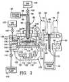
- FIG. 2is a cross-sectional view of the front portion of FIG. 1 as seen along lines 2 - 2 in FIG. 1.
- FIG. 3is a cross-sectional view of a single loadlock chamber and the high vacuum chamber of the front portion of FIG. 2 during a degassing operation.
- FIG. 4is the same view as FIG. 3 with the slot valve open and the high vacuum pump operating.
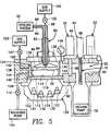
- FIG. 5is the same view as FIG. 3 during a cooling operation.
- the structural framework for a cluster toolcomprises a block 12 which includes a front portion 14 and a rear portion 16 .
- the front portionincludes a front wall 25 and a valve retaining wall 27 behind the front wall and is oriented somewhat parallel thereto.
- a pair of symmetrically opposed front portion side walls 13 , 13respectively merge into similarly opposed rear portion side walls 15 , 15 .
- the rear portion side wallsfurther merge rearwardly into a first diagonal wall 43 and a second diagonal wall 44 .
- the first and second diagonal wallsmerge into rear portion rear wall 40 , as shown in FIG. 1.
- the front portion side walls, rear portion side walls, first and second diagonal walls and rear portion rear wallall project about perpendicularly from bottom wall 62 .
- the front portion of the blockincludes two loadlock chambers 18 , 18 .
- the front portionfurther includes a high vacuum chamber 20 that is in communication with each respective loadlock chamber.
- Each loadlock chamberis selectively isolated from the high vacuum chamber with a slot valve 22 , 22 that is attached to top wall 56 , front wall 25 and valve retaining wall 27 in a manner hereinafter more fully described.
- the cluster toolincludes a pair of top cover plates 80 , 80 , with each top cover plate being attached to a respective front portion wall notch 79 and top wall notch 81 .
- the blockis made from an aluminum alloy.
- other types of machinable and/or castable metal alloysmay be used without departing from the scope of the present invention.
- a front loader 24is attached to front wall 25 of the block.
- the front loaderincludes a pair of bay doors 26 , 26 that correspond to front openings 28 , 28 in the front wall.
- the front openingsprovide an access through the front wall to the loadlock chambers.
- a plurality of cassette modules, of which module 30 a is representative,are attached to the front loader. These may be open wafer cassettes, SMIF (Standard Mechanical Interface Format) devices, FOUP's (Front Opening Universal Pods) or other structures known in the art for holding wafers.
- the front loaderhas internal structure (not shown), typically a front loader robot, for selectively transferring silicon wafers 32 from the cassette module through the bay doors to the loadlock chambers in a manner known in the prior art.
- An exemplary front loader of the type discussedis manufactured by Asyst® or Brooks Automation®.
- a plurality of processing pods 34are attached to the bottom wall of the block for accomplishing a sequence of vacuum processes on silicon wafer 32 .
- the rear portionalso includes an etching station 36 , which is electrically connected to a radio frequency (RF) matching unit/power supply 38 that is mounted on rear wall 40 of the block.
- RFradio frequency
- First rear cryopump 41is attached to rear diagonal wall 43
- second rear cryopump 42is attached to rear diagonal wall 44 of the block in communication with rear portion chamber 19 , as shown in FIG. 1.
- the first and second rear cryopumpsremove water vapor and gas molecules and establish a high vacuum in rear portion chamber 19 in a manner known in the prior art.
- a rear robot 46is centrally placed within the rear portion and attached to bottom wall 62 .
- the rear robotselectively accesses the loadlock chambers through loadlock access valves 52 , 52 that are attached to valve retaining wall 27 and front portion side walls 13 , 13 .
- the rear robotselectively transfers the wafer between loadlock chambers in the front portion of the cluster tool and the various processing pods in the rear portion chamber.
- the rear robotfurther transfers wafers between the vacuum process pods and the etching station, according to a predetermined algorithm that is programmed by a user (not shown) according to design requirements for the finished wafer.
- FIGS. 2 - 5the front portion of the block is shown with the high vacuum chamber 20 transversely centered within the front portion.
- the high vacuum chamberis between the loadlock chambers and also is in communication with each loadlock chamber.
- a slot valveis mounted between each loadlock chamber and the high vacuum chamber for selectively isolating each loadlock chamber from the high vacuum chamber.
- Each slot valveincludes a valve body 54 which is mounted within a recess 55 , 55 of top wall 56 of the block.
- the valve bodyincludes a valve stem 58 which is slidingly disposed within the valve body and has an extended position wherein the valve stem protrudes downwardly through the block into the high vacuum chamber. Valve stem 58 further has a retracted position wherein the valve stem is substantially encased by the valve body.
- a valve seat 60is machined into the inner surface of bottom wall 62 of the block opposite from the valve stem. As best seen in FIGS. 2 - 5 , when the valve stem 58 is in the retracted position within the valve body, a path of communication will exist between the corresponding loadlock chamber to the high vacuum chamber. When the valve stem is in the extended position, the valve stem will be seated in valve seat 60 , and the corresponding loadlock chamber will be isolated from the high vacuum chamber.
- a water pump 64which includes a refrigeration unit 68 and a cryoplate 70 is attached to top wall 56 of the block.
- the refrigeration unitextends upwardly therefrom.
- the cryoplateis in thermal communication with the refrigeration unit and extends downwardly therefrom through the top wall and into the high vacuum chamber.
- the refrigeration unitincludes a cryoplate cooling line 72 which extends from the refrigeration unit and is routed internally within the cryoplate.
- the cryoplate cooling linecirculates coolant (not shown) from the refrigeration unit through the cryoplate and back to the refrigeration unit, for maintaining a desired temperature on the cryoplate surface.
- a flat face 76 of the cryoplateis directly in front of the slot valve opening 74 of each loadlock chamber, for reasons to be described. With this configuration, a single water pump can serve a plurality of loadlock chambers.
- a high vacuum pump 78(depicted in schematic in FIGS. 2 - 5 ) is attached in communication with the high vacuum chamber for establishing a high vacuum therein in a manner known in the art. Once the corresponding slot valve is open, the loadlock chamber will be in communication with high vacuum chamber 20 , and a high vacuum will also be established in the corresponding loadlock chamber.
- the high vacuum pumpis a magnetic-levitation-bearing turbopump for producing a vacuum in the range of 10 ⁇ 4 to 10 ⁇ 8 torr.
- An exemplary type of pumpis manufactured by Varian®.
- the loadlock chamber of the present inventionalso includes a platen 82 .
- the platencomprises a platen stem 83 that merges into a lower bell portion 84 .
- the platen stemis oriented vertically and is slidingly disposed within an opening 85 in the top cover plate. With the platen stem oriented in this manner, the bell portion of the platen will be located within the loadlock chamber, and bell portion bottom surface 86 will be oriented horizontally within the loadlock chamber.
- a platen cooling system 92is connected to the platen stem.
- a platen cooling supply line 94is attached to the platen cooling system.
- the supply lineextends internally within the platen stem and merges into a platen cooling return line 96 .
- the platen cooling return line 96is also internally located within the platen stem and exits therefrom to connect with the platen cooling system.
- a platen gas supply line 98also is mounted internally within the platen stem.
- the platen gas supply lineextends from a platen gas supply 100 and terminates at the bottom surface of the platen.
- a platen gas line flow-controlling valve 102is attached to the platen gas line to selectively isolate the loadlock chamber from the platen gas supply and to control the flow of gas therefrom. This configuration allows a path of fluid communication to be selectively established between the platen gas supply and the loadlock chamber, for cooling a wafer as described below.
- a bellows 88is mounted to the top cover plate outer surface 90 , and the bellows is further attached in a surrounding relationship to the platen stem 83 .
- the bellowsallows for a sliding up-and-down movement of the platen, while at the same time maintaining vacuum integrity within the loadlock chamber.
- Each loadlock chamberincludes a chamber gas supply 103 for venting the loadlock chamber.
- a chamber gas supply line 105is attached to the chamber gas supply and terminates at the inner wall 108 of the loadlock chamber to provide a path of fluid communication between the chamber gas supply and the loadlock chamber.
- a vent valve 107 in the chamber gas supply line 105selectively isolates the chamber gas supply from the loadlock chamber.
- a gassuch as Argon or Nitrogen
- Argon or Nitrogenis used as the working gas for the platen gas supply, as well as the chamber gas supply. It is to be appreciated, however, that other gases could be used for performing the cooling function of the platen gas supply and the venting function of the chamber gas supply, as described above.
- each loadlock chamberincludes a respective roughing pump 104 for establishing an initial “rough” (approximately 10 ⁇ 2 to 10 ⁇ 3 torr) vacuum on the loadlock chamber.
- the roughing pumpis connected in fluid communication with the loadlock chamber via a roughing pump line 106 which extends through the front portion side wall and terminates at inner surface 108 of the front portion side wall.
- a roughing pump valve 110is placed in the roughing pump line to selectively isolate the roughing pump from the loadlock chamber.
- Each loadlock chamberhas a dedicated roughing pump. It is to be appreciated, however, that two loadlock chambers are never pumped to rough vacuum conditions at the same time, as hereinafter discussed in the Operation section of this specification. Accordingly, roughing pump line 106 could be routed to a plurality of loadlock chambers so that only one roughing pump can be used for a plurality of loadlock chambers.
- a bottom cover plate 112is attached to the bottom wall 62 of the block at a pair of opposing bottom wall niches 118 .
- the bottom cover platehas an underside 114 and a top side 116 and is attached to the bottom wall niches with the top side facing into the loadlock chamber.
- a heat lamp assembly 120is attached to the block.
- the heat lamp assemblycomprises a somewhat U-shaped reflector 122 with an upper reflector surface 124 and a lower encasement surface 126 , as well as a pair of opposing mounting surfaces 128 , 128 at the upwardly facing peripheral ends of the U-shaped reflector.
- a mounting bracket 130is attached to each respective mounting surface as shown in FIGS. 2 - 5 . The mounting brackets are secured to the bottom wall and the underside 116 of the bottom cover plate.
- a upper plurality of heat lamps 131 and a lower plurality of heat lamps 132are attached to the upper reflector surface 124 and radiate heat energy toward the bottom cover plate.
- the upper and lower pluralities of heat lampsare arranged in concentric circles, with the upper plurality circle being outside the lower plurality circle.
- the lamp intensity, distance between each lamp, and distance between each lamp and the bottom cover plateare adjusted to establish a plane of uniform radiation intensity within the loadlock chamber during illumination.
- the bottom cover plateis made of a material, such as quartz, which allows free passage of the heat lamp radiation into the loadlock chamber.
- the cluster tool of the present inventionfurther includes a tray 134 which is attached to the top cover plate for accurately positioning the wafer within the loadlock chamber.
- the traycomprises a plurality of rails 136 , 136 , that are mounted to the top cover plate so that they extend vertically downward therefrom in a surrounding relationship with the bell portion 84 .
- Each railhas an upper flange 138 and a lower flange 140 that project substantially perpendicularly from the rail, so that each rail has an inverted F-shape.
- the inverted F-shapeestablishes an upper flange horizontal surface 142 and a lower flange horizontal surface 144 for each rail.
- the tray rails 136extend downwardly into the loadlock chamber so that the upper flanges 138 of the trays are directly below the bell portion bottom surface 86 .
- the lower flanges 140are located directly above topside 114 of bottom cover plate 112 .
- the waferWhen a wafer is positioned at rest on the upper flange horizontal surfaces 142 , the wafer will be immediately proximate bell portion bottom surface 86 .
- the wafer 32is positioned at rest on the lower flange horizontal surfaces 144 , the wafer will be immediately above the bottom cover plate.
- the flangesalign the wafer so that it will be coextensive with the plane of uniform radiation intensity from the heat lamps discussed above. Accordingly, the wafer will be heated (and subsequently degassed) in a uniform manner.
- front loader 24transfers wafer 32 from a cassette module 30 , (SMIF device or FOUP) to one of the loadlock chambers 18 , 18 for processing. Initially, the wafer is placed on tray 134 within the loadlock chamber so that it rests on the lower flange horizontal surfaces 144 , as shown in FIG. 3. The associated slot valve 22 for the loadlock chamber is closed, and the roughing pump 104 is stopped. Next, the roughing pump valve 110 is opened and the roughing pump is actuated to establish an initial vacuum, preferably on the order of 10 ⁇ 2 to 10 ⁇ 3 torr as indicated by a chamber vacuum gage 146 .
- an initial vacuumpreferably on the order of 10 ⁇ 2 to 10 ⁇ 3 torr as indicated by a chamber vacuum gage 146 .
- the waferAs the roughing pump establishes an initial vacuum in the loadlock chamber, the wafer is simultaneously degassed by the heat lamp assembly 120 . To do this, the upper plurality and lower plurality of lamps are activated and direct heat energy through the bottom cover plate to the wafer. As the wafer is heated, entrained water molecules 148 in the wafer are released into the loadlock chamber whereby the wafer becomes degassed. The degassing of the wafer is accomplished simultaneously with the establishment of an initial rough vacuum on the loadlock chamber, to decrease overall processing time and increase the capacity of the cluster tool.
- the roughing pump valveis closed and the roughing pump is stopped.
- the adjacent high vacuum chamber 20is placed in communication with the loadlock chamber that contains the wafer by opening a corresponding slot valve 22 .
- the high vacuum pump(which preferably operates continuously) draws remaining gas and water vapor molecules from the loadlock chamber through the slot valve opening.
- the cryoplate face 76 of the water pump(which may also operates continuously), which is directly in front of the slot valve opening 74 .
- the water moleculescontact the cryoplate, they freeze thereon because the cryoplate is maintained at a temperature at, or below, their freezing point at high vacuum conditions.
- the removal of water vapor molecules from the wafer while the wafer is still in the loadlock chamberreduces the “water load” for the cryopumps 41 , 42 in the rear portion of the block and is one of the operative aspects of the invention.
- the loadlock access valve 52opens and the rear robot 46 transfers the wafer from the loadlock chamber to the vacuum processing pod(s) in the rear portion 16 of the block.
- the first and second rear cryopumpshave established a high vacuum in the rear portion. Since the rear portion is under high vacuum conditions similar to that of the loadlock chamber, the wafer remains under a high vacuum as it is transferred from the loadlock chamber to the rear portion. The wafer may then be transferred to all or part of the processing pods according to a predetermined algorithm that is based on design requirements for the finished wafer.
- the rear robotplaces the processed wafer from the vacuum processing station on upper flange surfaces 142 of tray 134 .
- Gas from platen gas supply system 100is transported through the platen stem and escapes from the lower bell portion 84 onto the wafer, cooling the wafer.
- front loader 24removes the cooled wafer from the loadlock chamber and replaces the finished wafer in the cassette module, SMIF device or FOUP.
Landscapes
- Engineering & Computer Science (AREA)
- Physics & Mathematics (AREA)
- Condensed Matter Physics & Semiconductors (AREA)
- General Physics & Mathematics (AREA)
- Manufacturing & Machinery (AREA)
- Computer Hardware Design (AREA)
- Microelectronics & Electronic Packaging (AREA)
- Power Engineering (AREA)
- Chemical & Material Sciences (AREA)
- Toxicology (AREA)
- Health & Medical Sciences (AREA)
- Materials Engineering (AREA)
- Mechanical Engineering (AREA)
- Metallurgy (AREA)
- Organic Chemistry (AREA)
- Chemical Kinetics & Catalysis (AREA)
- Physical Vapour Deposition (AREA)
- Container, Conveyance, Adherence, Positioning, Of Wafer (AREA)
- Earth Drilling (AREA)
- Physical Or Chemical Processes And Apparatus (AREA)
Abstract
Description
- The present invention pertains generally to cluster tools and processes which use a cluster tool. More particularly, the present invention pertains to cluster tools used in various processes for applying a coating to a silicon wafer. The invention is particularly, but not exclusively, useful as a cluster tool which simultaneously removes water vapor from a chamber containing a wafer while establishing a vacuum on the chamber to shorten the coating process and maximize wafer movement through the cluster tool.[0001]
- In order to more fully appreciate the cluster tool of the present invention, some discussion of the scientific principles behind a vacuum deposition process is helpful. In general, if two electrodes and the gas therebetween are at extreme low pressure, less than 1/110,000 of atmospheric pressure, the resistance of the gas will break down and allow current flow between the two electrodes. This is called a “glow discharge” in the prior art.[0002]
- Importantly, during the glow discharge process, the ionized gas atoms become attracted to and collide with the negative electrode (cathode), while the free electrons become attracted to and move towards the positive electrode (anode). Since electron mass is generally negligible relative to an atom, the electrons do not substantially affect the anode during collision. The mass of the ionized gas atoms, however, may be substantial relative to the mass of the atoms for the cathode material. Accordingly, when the ionized gas atoms collide with the cathode, the force of collision causes cathode material to be emitted. This phenomena is known as sputtering, or the removal of material from the cathode by ion bombardment during a glow discharge.[0003]
- The material that sputters from the cathode coats the surrounding surfaces. If a sputtering device is designed in a certain manner, a uniform, quality coating of the sputtered material can be deposited onto a substrate. The deposition of sputter material to form such a coating is often referred to as a vacuum deposition process.[0004]
- In the semiconductor industry, the vacuum process is used to coat silicon wafers, and certain devices that accomplish this result are known in the industry as cluster tools. To accomplish the vacuum process, however, the silicon wafer must be processed within a cluster tool capable of maintaining an extreme vacuum condition to ensure film purity. In addition to the vacuum issue, all water vapor molecules must be removed from the wafer to prevent contamination of the vacuum processes within the cluster tool, as water vapor is an undesirable process component that affects the quality of the finished wafer. Finally, outgoing wafers may be hot after undergoing a plurality of vacuum processes, and it is desirable to cool the wafers within the cluster tool, to reduce the risk of oxidation or corrosion.[0005]
- Cluster tools typically consist of a loadlock chamber for receiving wafers and a plurality of vacuum processing chambers for processing the wafers. In a conventional cluster tool, the wafers are introduced to the loadlock in a 25-wafer cassette module. Typically, the entire cassette module of wafers is placed in the loadlock chamber, and the loadlock chamber (along with the cassette module) is pumped down to high vacuum. This is a time consuming process. If the volume in the loadlock vacuum chamber could be minimized, and the vacuum condition established is merely a “rough” vacuum sufficient for further processing of the wafer within the cluster tool, the time required to establish a vacuum on the loadlock chamber will be reduced. Thus, the efficiency of the cluster tool would be increased.[0006]
- Prior art cluster tools typically have a dedicated degassing chamber for degassing the wafer, or removing the entrained water vapor molecules from the wafer. In the prior art, once the cassette module is under “rough” to mid-range vacuum conditions (10[0007]−2torr to 10−3torr, where 760 torr=1 Atm=atmospheric pressure), the wafers are successively placed in the dedicated degassing chamber for individual degassing prior to undergoing several vacuum processes. The dedicated degassing chamber is usually within the high vacuum body of the prior art cluster tool. What is desired is a cluster tool that degasses the wafers in the loadlock chamber under rough vacuum conditions. This eliminates the need for a dedicated processing position within the high vacuum body of the cluster tool.
- Degassed water vapor is removed from the high vacuum body of the cluster tool by cryopumps. A cryopump typically consists of a refrigeration unit that maintains an extremely low temperature on an array of metallic plates. The array is positioned in communication with the chamber and the water vapor molecules therein, and the water molecules impinge on the plate and are frozen thereto. These cryopumps are expensive and difficult to maintain. What is desired is a cluster tool that eliminates the need for a dedicated cryopump for each degassing chamber. One way to eliminate a dedicated cryopump is to remove water vapor molecules from the wafer while the wafer is at rough vacuum in the loadlock chamber. This will reduce the amount of residual water vapor in the proximity of the high vacuum body of the cluster. If this can be accomplished, vacuum quality and vacuum process quality can be enhanced. Also, the required number of cryopumps for the cluster tool would decrease, which further decreases the maintenance requirements for the cluster tool and increases the overall reliability of the tool.[0008]
- In the prior art, once each wafer from the cassette module has been degassed, the wafer is successively placed in a plurality of vacuum processing chambers and undergoes a plurality of vacuum processes. After completion of the processes, the wafer may be placed in a dedicated chamber for cooling. The wafer is then placed back into the cassette module, and another wafer is selected from the cassette to begin the processes discussed above. When all of the wafers in the cassette module have finished processing, the entire cassette module is removed from the loadlock chamber.[0009]
- With the above configuration, however, the first wafer spends more time cooling after its process is completed than the final wafer. Conversely, the last wafer to be processed has spent more time “drying” under vacuum before undergoing its vacuum processes. This can lead to a drift in measurable process quality in the wafers being loaded one at a time from the cassette module into the cluster tool for processing. This is known in the prior art as the “first wafer effect”. What is desired is a cluster tool with loadlock chambers that are capable of performing both degas and cooling functions during processing of the wafer, to standardize the amount of time each wafer spends at each step of the process and, thereby, to improve the consistency of the finished wafer quality.[0010]
- U.S. Pat. No. 5,516,732, which issued to Flegal for an invention entitled “Wafer Processing Machine Vacuum Front End Method and Apparatus”, discloses a station in which a preheating and degassing function are combined. Flegal, however, does not disclose a water pump positioned in fluid communication with the chamber for removal of the water vapor molecules at extreme vacuum. This is because the device, as disclosed by Flegal, is known as a “front end device” and must be connected to a cluster tool to perform a vacuum process. Accordingly, Flegal does not minimize the “water load” on the processing stations and does not minimize the number of cryopumps required to operate the cluster tool.[0011]
- U.S. Pat. No. 5,902,088, which issued to Fairbairn et al for an invention entitled “Single Loadlock Chamber With Wafer Cooling Function”, discloses a device in which a plurality of trays for receiving wafers are mounted within a loadlock structure, with the loadlock structure also performing a cooling function. The loadlock structure disclosed by Fairbairn, however, is sized to hold twelve to fourteen wafers, and establishing a vacuum on this size of a loadlock chamber presents the same problems that the present invention overcomes. Further, like Flegal, Fairbairn does not disclose a water pump attached in fluid communication with the loadlock structure and also does not minimize the number of water pumps required for the overall cluster tool.[0012]
- In view of the above, it is an object of the present invention to provide a cluster tool that increases throughput of silicon wafers by performing the degassing of the wafer simultaneously with establishing a vacuum for the loadlock chamber containing the wafer. This decreases the overall processing time and increases wafer throughput.[0013]
- It is another object of the present invention to provide a cluster tool that performs the degassing and the cooling steps within the loadlock chamber, to eliminate the need for separate dedicated degassing and cooling chambers. It is another object of the present invention to provide a cluster tool with a loadlock chamber that is sized to process a single wafer at a time, thereby minimizing the required volume to be placed under vacuum and eliminating what is known as “the first wafer effect”.[0014]
- It is another object of the present invention to provide a cluster tool with a single high vacuum chamber which services two loadlocks. This configuration minimizes the number of cryopumps required for the cluster tool and maximizes the reliability of the cluster tool.[0015]
- Each of the above features and objectives results in a cluster tool that is easier to operate and is more reliable. It is also simpler to manufacture at less cost.[0016]
- A cluster tool for performing a vacuum process on a silicon wafer in accordance with the present invention includes at least two loadlock chambers and a high vacuum chamber that are provided within a metal block. The loadlock chamber extend completely through the block from the block top surface to the block bottom surface. The high vacuum chamber is in fluid communication with each loadlock chamber in the block. An isolation means for selectively isolating each loadlock chamber from the high vacuum chamber, preferably a slot valve, is placed in each respective path of fluid communication. A respective roughing pump is connected in fluid communication with each loadlock chamber for establishing an initial vacuum therein.[0017]
- The cluster tool of the present invention further includes a high vacuum pump and a water pump. The high vacuum pump is mounted to the block in fluid communication with the high vacuum chamber. The water pump comprises a refrigeration unit and a cryoplate. The refrigeration unit is mounted to the block, while the cryoplate is attached in thermal communication with the refrigeration unit. More specifically, the cryoplate projects from the refrigeration unit through the block and into the high vacuum chamber.[0018]
- The cryoplate is positioned within the high vacuum chamber so that it is between the loadlock chambers and is directly in front of each respective slot valve. When a loadlock chamber is placed in fluid communication with the high vacuum chamber, the high vacuum pump draws water vapor molecules from the loadlock chamber. The water vapor molecules impinge upon the cryoplate and freeze thereon. The orientation of the high vacuum pump and water pump between the loadlock chamber minimizes the number of water pumps and high vacuum pumps needed to establish and maintain a high vacuum on the loadlock chambers.[0019]
- The loadlock chambers are sized and shaped to accommodate a single wafer in order to minimize the required volume which is to be pumped to high vacuum. Each loadlock chamber has a top wall, a bottom wall and side walls and includes a platen comprising a stem that merges into a bell portion, with the bell portion terminating at a flat bottom surface. The platen stem is slidingly positioned within an opening in the top wall and projects downwardly into the loadloack chamber so that the bell portion is completely within the loadlock chamber.[0020]
- The loadlock chamber of the present invention also includes a holding means that is adapted to hold a silicon wafer, and a plurality of heat lamps. The holding means comprises a tray with a plurality of rails that extend downwardly from the top wall in a surrounding relationship with the bell portion of the platen. Each rail has an upper flange and a lower flange that project perpendicularly from the rail, thereby establishing an inverted F-shape for the rail. When the wafer is resting on the upper flanges, the wafer is immediately proximate the bell portion bottom surface. When the wafer is resting upon the lower flanges, the wafer is spaced-apart from the platen bottom surface.[0021]
- The loadlock chamber of the present invention further includes a plurality of heat lamps that are mounted to the bottom wall of the loadlock chamber so that they illuminate upwardly into the loadlock chamber. When the wafer is resting on the lower flanges, the wafer is coextensive with a focal plane of uniform radiation intensity from the heat lamps. The heat lamps, tray and platen combine to establish a loadlock chamber which can perform both a cooling and a degassing function, thereby reducing the number of loadlock chambers required for the cluster tool.[0022]
- For the method of the present invention, the wafer is placed in the loadlock chamber on the lower flanges, and an initial vacuum is established by the corresponding roughing pump. Simultaneously, the heat lamps are activated to radiate heat energy to the wafer, thereby causing the release of water vapor molecules from the wafer, thereby degassing the wafer. Next, the roughing pump is isolated from the loadlock chamber, the lamps are preferably turned off, and the loadlock chamber is aligned in fluid communication with the high vacuum chamber by opening the corresponding slot valve. A high vacuum pump produces a high vacuum in the high vacuum chamber and draws residual water vapor molecules from the loadlock chamber into the high vacuum chamber.[0023]
- As the molecules are drawn into the high vacuum chamber, the molecules impinge on the cryoplate, as discussed above, and are frozen onto the cryoplate. In this manner, the silicon wafer undergoes an initial degassing and a high vacuum is quickly and easily established in the loadlock chamber. Thereafter, the wafer undergoes a plurality of manufacturing processes in a manner known in the art.[0024]
- The novel features of this invention will be best understood from the accompanying drawings, taken in conjunction with the accompanying description, in which similar characters refer to similar parts, and in which:[0025]
- FIG. 1 is a top plan view of the cluster tool of the present invention with a large portion of the top wall of the tool removed for clarity.[0026]
- FIG. 2 is a cross-sectional view of the front portion of FIG. 1 as seen along lines[0027]2-2 in FIG. 1.
- FIG. 3 is a cross-sectional view of a single loadlock chamber and the high vacuum chamber of the front portion of FIG. 2 during a degassing operation.[0028]
- FIG. 4 is the same view as FIG. 3 with the slot valve open and the high vacuum pump operating.[0029]
- FIG. 5 is the same view as FIG. 3 during a cooling operation.[0030]
- With reference now to FIGS. 1 and 2, the cluster tool of the present invention is shown and generally designated by[0031]
reference character 10. As shown, the structural framework for a cluster tool comprises ablock 12 which includes afront portion 14 and arear portion 16. The front portion includes afront wall 25 and avalve retaining wall 27 behind the front wall and is oriented somewhat parallel thereto. A pair of symmetrically opposed frontportion side walls portion side walls diagonal wall 43 and a seconddiagonal wall 44. The first and second diagonal walls merge into rear portionrear wall 40, as shown in FIG. 1. The front portion side walls, rear portion side walls, first and second diagonal walls and rear portion rear wall all project about perpendicularly frombottom wall 62. - The front portion of the block includes two[0032]
loadlock chambers high vacuum chamber 20 that is in communication with each respective loadlock chamber. Each loadlock chamber is selectively isolated from the high vacuum chamber with aslot valve top wall 56,front wall 25 andvalve retaining wall 27 in a manner hereinafter more fully described. By referring to both FIGS. 1 and 2, it can be seen that the cluster tool includes a pair oftop cover plates portion wall notch 79 andtop wall notch 81. - In the preferred embodiment, the block is made from an aluminum alloy. However, other types of machinable and/or castable metal alloys may be used without departing from the scope of the present invention.[0033]
- A[0034]
front loader 24 is attached tofront wall 25 of the block. The front loader includes a pair ofbay doors front openings silicon wafers 32 from the cassette module through the bay doors to the loadlock chambers in a manner known in the prior art. An exemplary front loader of the type discussed is manufactured by Asyst® or Brooks Automation®. - In[0035]
rear portion 16, a plurality ofprocessing pods 34 are attached to the bottom wall of the block for accomplishing a sequence of vacuum processes onsilicon wafer 32. The rear portion also includes anetching station 36, which is electrically connected to a radio frequency (RF) matching unit/power supply 38 that is mounted onrear wall 40 of the block. - First[0036]
rear cryopump 41 is attached to reardiagonal wall 43, and secondrear cryopump 42 is attached to reardiagonal wall 44 of the block in communication with rear portion chamber19, as shown in FIG. 1. The first and second rear cryopumps remove water vapor and gas molecules and establish a high vacuum in rear portion chamber19 in a manner known in the prior art. - As further seen in FIG. 1, a[0037]
rear robot 46 is centrally placed within the rear portion and attached tobottom wall 62. The rear robot selectively accesses the loadlock chambers throughloadlock access valves valve retaining wall 27 and frontportion side walls - Referring now to FIGS.[0038]2-5, the front portion of the block is shown with the
high vacuum chamber 20 transversely centered within the front portion. As stated above, the high vacuum chamber is between the loadlock chambers and also is in communication with each loadlock chamber. - As also stated above, a slot valve is mounted between each loadlock chamber and the high vacuum chamber for selectively isolating each loadlock chamber from the high vacuum chamber. Each slot valve includes a[0039]
valve body 54 which is mounted within a recess55,55 oftop wall 56 of the block. - The valve body includes a[0040]
valve stem 58 which is slidingly disposed within the valve body and has an extended position wherein the valve stem protrudes downwardly through the block into the high vacuum chamber. Valve stem58 further has a retracted position wherein the valve stem is substantially encased by the valve body. - For each slot valve, a[0041]
valve seat 60 is machined into the inner surface ofbottom wall 62 of the block opposite from the valve stem. As best seen in FIGS.2-5, when thevalve stem 58 is in the retracted position within the valve body, a path of communication will exist between the corresponding loadlock chamber to the high vacuum chamber. When the valve stem is in the extended position, the valve stem will be seated invalve seat 60, and the corresponding loadlock chamber will be isolated from the high vacuum chamber. - A[0042]
water pump 64 which includes arefrigeration unit 68 and acryoplate 70 is attached totop wall 56 of the block. The refrigeration unit extends upwardly therefrom. The cryoplate is in thermal communication with the refrigeration unit and extends downwardly therefrom through the top wall and into the high vacuum chamber. - The refrigeration unit includes a[0043]
cryoplate cooling line 72 which extends from the refrigeration unit and is routed internally within the cryoplate. The cryoplate cooling line circulates coolant (not shown) from the refrigeration unit through the cryoplate and back to the refrigeration unit, for maintaining a desired temperature on the cryoplate surface. In the preferred embodiment, the cryoplate is maintained at a temperature of approximately one hundred degrees Kelvin (T=100° K). It is to be appreciated that other configurations for the heat exchanger and cryoplate are envisioned, provided the cryoplate can maintain the desired low temperatures. - A[0044]
flat face 76 of the cryoplate is directly in front of the slot valve opening74 of each loadlock chamber, for reasons to be described. With this configuration, a single water pump can serve a plurality of loadlock chambers. - A high vacuum pump[0045]78 (depicted in schematic in FIGS.2-5) is attached in communication with the high vacuum chamber for establishing a high vacuum therein in a manner known in the art. Once the corresponding slot valve is open, the loadlock chamber will be in communication with
high vacuum chamber 20, and a high vacuum will also be established in the corresponding loadlock chamber. In a preferred embodiment, the high vacuum pump is a magnetic-levitation-bearing turbopump for producing a vacuum in the range of 10−4to 10−8torr. An exemplary type of pump is manufactured by Varian®. - With further reference to FIGS.[0046]2-5, the loadlock chamber of the present invention also includes a
platen 82. The platen comprises aplaten stem 83 that merges into alower bell portion 84. The platen stem is oriented vertically and is slidingly disposed within anopening 85 in the top cover plate. With the platen stem oriented in this manner, the bell portion of the platen will be located within the loadlock chamber, and bellportion bottom surface 86 will be oriented horizontally within the loadlock chamber. - To maintain a predetermined platen temperature, a[0047]
platen cooling system 92 is connected to the platen stem. Specifically, a platencooling supply line 94 is attached to the platen cooling system. The supply line extends internally within the platen stem and merges into a platencooling return line 96. The platencooling return line 96 is also internally located within the platen stem and exits therefrom to connect with the platen cooling system. With this configuration, refrigerant (not shown) is circulated from the platen cooling system internally through the platen stem and back to the platen cooling system for cooling the platen. - A platen[0048]
gas supply line 98 also is mounted internally within the platen stem. The platen gas supply line extends from aplaten gas supply 100 and terminates at the bottom surface of the platen. A platen gas line flow-controllingvalve 102 is attached to the platen gas line to selectively isolate the loadlock chamber from the platen gas supply and to control the flow of gas therefrom. This configuration allows a path of fluid communication to be selectively established between the platen gas supply and the loadlock chamber, for cooling a wafer as described below. - A bellows[0049]88 is mounted to the top cover plate
outer surface 90, and the bellows is further attached in a surrounding relationship to theplaten stem 83. The bellows allows for a sliding up-and-down movement of the platen, while at the same time maintaining vacuum integrity within the loadlock chamber. - Each loadlock chamber includes a[0050]
chamber gas supply 103 for venting the loadlock chamber. A chambergas supply line 105 is attached to the chamber gas supply and terminates at theinner wall 108 of the loadlock chamber to provide a path of fluid communication between the chamber gas supply and the loadlock chamber. Avent valve 107 in the chambergas supply line 105 selectively isolates the chamber gas supply from the loadlock chamber. - In the preferred embodiment, a gas, such as Argon or Nitrogen, is used as the working gas for the platen gas supply, as well as the chamber gas supply. It is to be appreciated, however, that other gases could be used for performing the cooling function of the platen gas supply and the venting function of the chamber gas supply, as described above.[0051]
- With reference to FIG. 2, each loadlock chamber includes a[0052]
respective roughing pump 104 for establishing an initial “rough” (approximately 10−2to 10−3torr) vacuum on the loadlock chamber. The roughing pump is connected in fluid communication with the loadlock chamber via aroughing pump line 106 which extends through the front portion side wall and terminates atinner surface 108 of the front portion side wall. Aroughing pump valve 110 is placed in the roughing pump line to selectively isolate the roughing pump from the loadlock chamber. - Each loadlock chamber has a dedicated roughing pump. It is to be appreciated, however, that two loadlock chambers are never pumped to rough vacuum conditions at the same time, as hereinafter discussed in the Operation section of this specification. Accordingly, roughing[0053]
pump line 106 could be routed to a plurality of loadlock chambers so that only one roughing pump can be used for a plurality of loadlock chambers. - A[0054]
bottom cover plate 112 is attached to thebottom wall 62 of the block at a pair of opposingbottom wall niches 118. The bottom cover plate has anunderside 114 and atop side 116 and is attached to the bottom wall niches with the top side facing into the loadlock chamber. Below the bottom cover plate, aheat lamp assembly 120 is attached to the block. - The heat lamp assembly comprises a somewhat[0055]
U-shaped reflector 122 with anupper reflector surface 124 and alower encasement surface 126, as well as a pair of opposing mountingsurfaces bracket 130 is attached to each respective mounting surface as shown in FIGS.2-5. The mounting brackets are secured to the bottom wall and theunderside 116 of the bottom cover plate. - A upper plurality of[0056]
heat lamps 131 and a lower plurality ofheat lamps 132 are attached to theupper reflector surface 124 and radiate heat energy toward the bottom cover plate. The upper and lower pluralities of heat lamps are arranged in concentric circles, with the upper plurality circle being outside the lower plurality circle. The lamp intensity, distance between each lamp, and distance between each lamp and the bottom cover plate are adjusted to establish a plane of uniform radiation intensity within the loadlock chamber during illumination. The bottom cover plate is made of a material, such as quartz, which allows free passage of the heat lamp radiation into the loadlock chamber. - The cluster tool of the present invention further includes a[0057]
tray 134 which is attached to the top cover plate for accurately positioning the wafer within the loadlock chamber. The tray comprises a plurality ofrails bell portion 84. Each rail has anupper flange 138 and alower flange 140 that project substantially perpendicularly from the rail, so that each rail has an inverted F-shape. The inverted F-shape establishes an upper flangehorizontal surface 142 and a lower flangehorizontal surface 144 for each rail. - The tray rails[0058]136 extend downwardly into the loadlock chamber so that the
upper flanges 138 of the trays are directly below the bellportion bottom surface 86. Thelower flanges 140 are located directly above topside114 ofbottom cover plate 112. When a wafer is positioned at rest on the upper flangehorizontal surfaces 142, the wafer will be immediately proximate bellportion bottom surface 86. When thewafer 32 is positioned at rest on the lower flangehorizontal surfaces 144, the wafer will be immediately above the bottom cover plate. The flanges align the wafer so that it will be coextensive with the plane of uniform radiation intensity from the heat lamps discussed above. Accordingly, the wafer will be heated (and subsequently degassed) in a uniform manner. - To operate the cluster tool,[0059]
front loader 24transfers wafer 32 from a cassette module30, (SMIF device or FOUP) to one of theloadlock chambers tray 134 within the loadlock chamber so that it rests on the lower flangehorizontal surfaces 144, as shown in FIG. 3. The associatedslot valve 22 for the loadlock chamber is closed, and theroughing pump 104 is stopped. Next, theroughing pump valve 110 is opened and the roughing pump is actuated to establish an initial vacuum, preferably on the order of 10−2to 10−3torr as indicated by achamber vacuum gage 146. - As the roughing pump establishes an initial vacuum in the loadlock chamber, the wafer is simultaneously degassed by the[0060]
heat lamp assembly 120. To do this, the upper plurality and lower plurality of lamps are activated and direct heat energy through the bottom cover plate to the wafer. As the wafer is heated, entrainedwater molecules 148 in the wafer are released into the loadlock chamber whereby the wafer becomes degassed. The degassing of the wafer is accomplished simultaneously with the establishment of an initial rough vacuum on the loadlock chamber, to decrease overall processing time and increase the capacity of the cluster tool. - Once the initial vacuum is established on the loadlock chamber, the roughing pump valve is closed and the roughing pump is stopped. The adjacent[0061]
high vacuum chamber 20 is placed in communication with the loadlock chamber that contains the wafer by opening acorresponding slot valve 22. - Referring to FIG. 4, as the slot valve opens, the high vacuum pump (which preferably operates continuously) draws remaining gas and water vapor molecules from the loadlock chamber through the slot valve opening. As the water molecules are drawn into the high vacuum chamber from the slot valve opening, they impinge directly onto the cryoplate face[0062]76 of the water pump (which may also operates continuously), which is directly in front of the
slot valve opening 74. As the water molecules contact the cryoplate, they freeze thereon because the cryoplate is maintained at a temperature at, or below, their freezing point at high vacuum conditions. The removal of water vapor molecules from the wafer while the wafer is still in the loadlock chamber reduces the “water load” for thecryopumps - After the wafer has been processed in the loadlock chamber as described above, the[0063]
loadlock access valve 52 opens and therear robot 46 transfers the wafer from the loadlock chamber to the vacuum processing pod(s) in therear portion 16 of the block. As discussed above, the first and second rear cryopumps have established a high vacuum in the rear portion. Since the rear portion is under high vacuum conditions similar to that of the loadlock chamber, the wafer remains under a high vacuum as it is transferred from the loadlock chamber to the rear portion. The wafer may then be transferred to all or part of the processing pods according to a predetermined algorithm that is based on design requirements for the finished wafer. - After the wafer has undergone the last manufacturing procedure, the rear robot places the processed wafer from the vacuum processing station on upper flange surfaces[0064]142 of
tray 134. Gas from platengas supply system 100 is transported through the platen stem and escapes from thelower bell portion 84 onto the wafer, cooling the wafer. Similarly, thevent valve 107 is opened and gas fromchamber gas supply 103 is vented into the loadlock chamber, in order to raise the loadlock pressure to one atmosphere (P=1 atm). Because the loadlock chamber volume is minimized, less gas is required to vent the chamber, and the wafer is cooled and unloaded more quickly than prior art systems. - Once the wafer has cooled,[0065]
front loader 24 removes the cooled wafer from the loadlock chamber and replaces the finished wafer in the cassette module, SMIF device or FOUP. - While the particular cluster tool, as herein shown and disclosed in detail, is fully capable of obtaining the objects and providing the advantages above stated, it is to be understood that the presently preferred embodiments are merely illustrative of the invention. As such, no limitations are intended other than as defined in the appended claims.[0066]
Claims (15)
Priority Applications (10)
| Application Number | Priority Date | Filing Date | Title |
|---|---|---|---|
| US09/798,048US6562141B2 (en) | 2000-07-03 | 2001-03-05 | Dual degas/cool loadlock cluster tool |
| EP01950859AEP1303449B1 (en) | 2000-07-03 | 2001-07-02 | Dual degas/cool loadlock cluster tool |
| CNB018022855ACN1193922C (en) | 2000-07-03 | 2001-07-02 | Degassing and cooling combination locking device |
| JP2002507709AJP5048198B2 (en) | 2000-07-03 | 2001-07-02 | Dual Degas / Cooling Load Lock Cluster Tool |
| PCT/US2001/021206WO2002002445A1 (en) | 2000-07-03 | 2001-07-02 | Dual degas/cool loadlock cluster tool |
| HK03104372.7AHK1051992A1 (en) | 2000-07-03 | 2001-07-02 | Dual degas/cool loadlock cluster tool |
| KR1020027002882AKR20020047143A (en) | 2000-07-03 | 2001-07-02 | Dual degas/cool loadlock cluster tool |
| DE60119119TDE60119119T2 (en) | 2000-07-03 | 2001-07-02 | Cluster tool with two degassing / cooling lock chambers |
| AT01950859TATE324341T1 (en) | 2000-07-03 | 2001-07-02 | MULTI-CHAMBER REACTOR WITH TWO VENT/COOLING LOCK CHAMBERS |
| US10/290,546US20030066606A1 (en) | 2000-07-03 | 2002-11-08 | Dual wafer position loadlock chamber |
Applications Claiming Priority (2)
| Application Number | Priority Date | Filing Date | Title |
|---|---|---|---|
| US09/609,733US6235656B1 (en) | 2000-07-03 | 2000-07-03 | Dual degas/cool loadlock cluster tool |
| US09/798,048US6562141B2 (en) | 2000-07-03 | 2001-03-05 | Dual degas/cool loadlock cluster tool |
Related Parent Applications (1)
| Application Number | Title | Priority Date | Filing Date |
|---|---|---|---|
| US09/609,733DivisionUS6235656B1 (en) | 2000-07-03 | 2000-07-03 | Dual degas/cool loadlock cluster tool |
Related Child Applications (1)
| Application Number | Title | Priority Date | Filing Date |
|---|---|---|---|
| US10/290,546DivisionUS20030066606A1 (en) | 2000-07-03 | 2002-11-08 | Dual wafer position loadlock chamber |
Publications (2)
| Publication Number | Publication Date |
|---|---|
| US20020000194A1true US20020000194A1 (en) | 2002-01-03 |
| US6562141B2 US6562141B2 (en) | 2003-05-13 |
Family
ID=27086108
Family Applications (2)
| Application Number | Title | Priority Date | Filing Date |
|---|---|---|---|
| US09/798,048Expired - LifetimeUS6562141B2 (en) | 2000-07-03 | 2001-03-05 | Dual degas/cool loadlock cluster tool |
| US10/290,546AbandonedUS20030066606A1 (en) | 2000-07-03 | 2002-11-08 | Dual wafer position loadlock chamber |
Family Applications After (1)
| Application Number | Title | Priority Date | Filing Date |
|---|---|---|---|
| US10/290,546AbandonedUS20030066606A1 (en) | 2000-07-03 | 2002-11-08 | Dual wafer position loadlock chamber |
Country Status (9)
| Country | Link |
|---|---|
| US (2) | US6562141B2 (en) |
| EP (1) | EP1303449B1 (en) |
| JP (1) | JP5048198B2 (en) |
| KR (1) | KR20020047143A (en) |
| CN (1) | CN1193922C (en) |
| AT (1) | ATE324341T1 (en) |
| DE (1) | DE60119119T2 (en) |
| HK (1) | HK1051992A1 (en) |
| WO (1) | WO2002002445A1 (en) |
Cited By (15)
| Publication number | Priority date | Publication date | Assignee | Title |
|---|---|---|---|---|
| US20050037521A1 (en)* | 2003-08-15 | 2005-02-17 | Uwe Wellhausen | Methods and apparatus for processing semiconductor devices by gas annealing |
| US6919271B2 (en) | 1998-11-20 | 2005-07-19 | Mattson Technology, Inc. | Method for rapidly heating and cooling semiconductor wafers |
| US20080282710A1 (en)* | 2007-05-15 | 2008-11-20 | Bartlett Allen J | Integral facet cryopump, water vapor pump, or high vacuum pump |
| DE10323295B4 (en)* | 2003-05-21 | 2009-04-16 | Von Ardenne Anlagentechnik Gmbh | Vacuum coating system and method for coating substrates |
| US20100055347A1 (en)* | 2008-08-29 | 2010-03-04 | Tokyo Electron Limited | Activated gas injector, film deposition apparatus, and film deposition method |
| US20110031214A1 (en)* | 2009-08-06 | 2011-02-10 | Jisoo Kim | Vacuum processing chambers incorporating a moveable flow equalizer |
| US20110100489A1 (en)* | 2009-11-04 | 2011-05-05 | Tokyo Electron Limited | Substrate process apparatus, substrate process method, and computer readable storage medium |
| US20110126985A1 (en)* | 2009-12-02 | 2011-06-02 | Tokyo Electron Limited | Substrate processing apparatus |
| US20110139074A1 (en)* | 2009-12-10 | 2011-06-16 | Tokyo Electron Limited | Film deposition apparatus |
| US20110214611A1 (en)* | 2008-11-14 | 2011-09-08 | Tokyo Electron Limited | Film deposition apparatus |
| DE102012104013A1 (en)* | 2012-05-08 | 2013-11-14 | Schmid Vacuum Technology Gmbh | High vacuum system and method for evacuation |
| WO2016184487A1 (en)* | 2015-05-15 | 2016-11-24 | Applied Materials, Inc. | Load lock chamber, vacuum processing system with load lock chamber and method for evacuating a load lock chamber |
| DE102015110711A1 (en) | 2015-07-02 | 2017-01-05 | Endress+Hauser Flowtec Ag | MEMS sensor for measuring at least one measured variable of a flowing fluid |
| US9627324B2 (en) | 2009-11-17 | 2017-04-18 | Evatec Ag | Apparatus and method for processing a substrate |
| CN114875381A (en)* | 2022-05-13 | 2022-08-09 | 东莞市华升真空镀膜科技有限公司 | Vacuum coating cavity and vacuum coating equipment |
Families Citing this family (46)
| Publication number | Priority date | Publication date | Assignee | Title |
|---|---|---|---|---|
| US6800172B2 (en)* | 2002-02-22 | 2004-10-05 | Micron Technology, Inc. | Interfacial structure for semiconductor substrate processing chambers and substrate transfer chambers and for semiconductor substrate processing chambers and accessory attachments, and semiconductor substrate processor |
| US6814813B2 (en)* | 2002-04-24 | 2004-11-09 | Micron Technology, Inc. | Chemical vapor deposition apparatus |
| US6858264B2 (en)* | 2002-04-24 | 2005-02-22 | Micron Technology, Inc. | Chemical vapor deposition methods |
| US6838114B2 (en) | 2002-05-24 | 2005-01-04 | Micron Technology, Inc. | Methods for controlling gas pulsing in processes for depositing materials onto micro-device workpieces |
| US6821347B2 (en) | 2002-07-08 | 2004-11-23 | Micron Technology, Inc. | Apparatus and method for depositing materials onto microelectronic workpieces |
| US6955725B2 (en) | 2002-08-15 | 2005-10-18 | Micron Technology, Inc. | Reactors with isolated gas connectors and methods for depositing materials onto micro-device workpieces |
| US6926775B2 (en)* | 2003-02-11 | 2005-08-09 | Micron Technology, Inc. | Reactors with isolated gas connectors and methods for depositing materials onto micro-device workpieces |
| SG115629A1 (en) | 2003-03-11 | 2005-10-28 | Asml Netherlands Bv | Method and apparatus for maintaining a machine part |
| SG115631A1 (en) | 2003-03-11 | 2005-10-28 | Asml Netherlands Bv | Lithographic projection assembly, load lock and method for transferring objects |
| US7335396B2 (en) | 2003-04-24 | 2008-02-26 | Micron Technology, Inc. | Methods for controlling mass flow rates and pressures in passageways coupled to reaction chambers and systems for depositing material onto microfeature workpieces in reaction chambers |
| US7235138B2 (en) | 2003-08-21 | 2007-06-26 | Micron Technology, Inc. | Microfeature workpiece processing apparatus and methods for batch deposition of materials on microfeature workpieces |
| US7344755B2 (en) | 2003-08-21 | 2008-03-18 | Micron Technology, Inc. | Methods and apparatus for processing microfeature workpieces; methods for conditioning ALD reaction chambers |
| US7422635B2 (en) | 2003-08-28 | 2008-09-09 | Micron Technology, Inc. | Methods and apparatus for processing microfeature workpieces, e.g., for depositing materials on microfeature workpieces |
| US7056806B2 (en) | 2003-09-17 | 2006-06-06 | Micron Technology, Inc. | Microfeature workpiece processing apparatus and methods for controlling deposition of materials on microfeature workpieces |
| US7282239B2 (en)* | 2003-09-18 | 2007-10-16 | Micron Technology, Inc. | Systems and methods for depositing material onto microfeature workpieces in reaction chambers |
| US7323231B2 (en) | 2003-10-09 | 2008-01-29 | Micron Technology, Inc. | Apparatus and methods for plasma vapor deposition processes |
| US7581511B2 (en) | 2003-10-10 | 2009-09-01 | Micron Technology, Inc. | Apparatus and methods for manufacturing microfeatures on workpieces using plasma vapor processes |
| US7647886B2 (en) | 2003-10-15 | 2010-01-19 | Micron Technology, Inc. | Systems for depositing material onto workpieces in reaction chambers and methods for removing byproducts from reaction chambers |
| US7258892B2 (en) | 2003-12-10 | 2007-08-21 | Micron Technology, Inc. | Methods and systems for controlling temperature during microfeature workpiece processing, e.g., CVD deposition |
| US7906393B2 (en) | 2004-01-28 | 2011-03-15 | Micron Technology, Inc. | Methods for forming small-scale capacitor structures |
| US7584942B2 (en) | 2004-03-31 | 2009-09-08 | Micron Technology, Inc. | Ampoules for producing a reaction gas and systems for depositing materials onto microfeature workpieces in reaction chambers |
| US8133554B2 (en) | 2004-05-06 | 2012-03-13 | Micron Technology, Inc. | Methods for depositing material onto microfeature workpieces in reaction chambers and systems for depositing materials onto microfeature workpieces |
| US7699932B2 (en) | 2004-06-02 | 2010-04-20 | Micron Technology, Inc. | Reactors, systems and methods for depositing thin films onto microfeature workpieces |
| KR100648261B1 (en)* | 2004-08-16 | 2006-11-23 | 삼성전자주식회사 | Load lock module to effectively remove wafer fume |
| US7972441B2 (en)* | 2005-04-05 | 2011-07-05 | Applied Materials, Inc. | Thermal oxidation of silicon using ozone |
| JP2008034740A (en)* | 2006-07-31 | 2008-02-14 | Dainippon Screen Mfg Co Ltd | Load lock device, substrate processing apparatus and substrate processing system equipped therewith |
| US20080025823A1 (en)* | 2006-07-31 | 2008-01-31 | Masahiko Harumoto | Load lock device, and substrate processing apparatus and substrate processing system including the same |
| US20090194027A1 (en)* | 2008-02-01 | 2009-08-06 | Applied Materials, Inc. | Twin-type coating device with improved separating plate |
| US8034691B2 (en)* | 2008-08-18 | 2011-10-11 | Macronix International Co., Ltd. | HDP-CVD process, filling-in process utilizing HDP-CVD, and HDP-CVD system |
| KR20110131291A (en)* | 2009-03-16 | 2011-12-06 | 알타 디바이씨즈, 인크. | Heating lamp system and its method |
| KR101074083B1 (en) | 2009-07-27 | 2011-10-17 | 피에스케이 주식회사 | Roadlock chamber and substrate treating facility including the chamber, and method for treating substrate with the facility |
| KR100996210B1 (en)* | 2010-04-12 | 2010-11-24 | 세메스 주식회사 | Gas injection unit and apparatus and method for depositing thin layer with the same |
| US20110269314A1 (en)* | 2010-04-30 | 2011-11-03 | Applied Materials, Inc. | Process chambers having shared resources and methods of use thereof |
| KR101327458B1 (en)* | 2012-01-10 | 2013-11-08 | 주식회사 유진테크 | Showerhead having cooling system and substrate processing apparatus including the showerhead |
| CN105706227B (en) | 2013-11-04 | 2019-11-26 | 应用材料公司 | Transfer chamber with increased number of sides, semiconductor device fabrication processing tool and processing method |
| CN104746008B (en)* | 2013-12-30 | 2017-06-06 | 北京北方微电子基地设备工艺研究中心有限责任公司 | Go to gas chamber |
| US9453614B2 (en)* | 2014-03-17 | 2016-09-27 | Lam Research Corporation | Systems and methods for cooling and removing reactants from a substrate processing chamber |
| JP6408904B2 (en)* | 2014-12-25 | 2018-10-17 | 東京エレクトロン株式会社 | Vacuuming method and vacuum processing apparatus |
| TW201639063A (en) | 2015-01-22 | 2016-11-01 | 應用材料股份有限公司 | Batch heating and cooling chamber or loadlock |
| CN106298585B (en)* | 2015-06-03 | 2020-10-16 | 北京北方华创微电子装备有限公司 | Cavity and semiconductor processing equipment |
| CN107958851B (en)* | 2016-10-14 | 2022-08-16 | 北京北方华创微电子装备有限公司 | Transmission chamber and semiconductor processing equipment |
| US11802340B2 (en)* | 2016-12-12 | 2023-10-31 | Applied Materials, Inc. | UHV in-situ cryo-cool chamber |
| KR20200000638A (en)* | 2018-06-25 | 2020-01-03 | 주성엔지니어링(주) | Appratus and method for processing substrate |
| WO2021044622A1 (en)* | 2019-09-06 | 2021-03-11 | キヤノンアネルバ株式会社 | Load lock device |
| CN113265626B (en)* | 2020-02-14 | 2023-06-16 | 芝浦机械电子装置株式会社 | Film forming apparatus and method for removing moisture in film forming apparatus |
| JP7451436B2 (en) | 2020-02-14 | 2024-03-18 | 芝浦メカトロニクス株式会社 | Film deposition equipment and method for removing moisture from film deposition equipment |
Family Cites Families (24)
| Publication number | Priority date | Publication date | Assignee | Title |
|---|---|---|---|---|
| US4504194A (en) | 1982-05-24 | 1985-03-12 | Varian Associates, Inc. | Air lock vacuum pumping methods and apparatus |
| US5259881A (en) | 1991-05-17 | 1993-11-09 | Materials Research Corporation | Wafer processing cluster tool batch preheating and degassing apparatus |
| KR900005610Y1 (en) | 1987-04-16 | 1990-06-28 | 이형곤 | Dula vacuum system |
| US4923584A (en)* | 1988-10-31 | 1990-05-08 | Eaton Corporation | Sealing apparatus for a vacuum processing system |
| US5516732A (en) | 1992-12-04 | 1996-05-14 | Sony Corporation | Wafer processing machine vacuum front end method and apparatus |
| DE69304038T2 (en)* | 1993-01-28 | 1996-12-19 | Applied Materials Inc | Device for a vacuum process with improved throughput |
| US5345534A (en)* | 1993-03-29 | 1994-09-06 | Texas Instruments Incorporated | Semiconductor wafer heater with infrared lamp module with light blocking means |
| US5592581A (en)* | 1993-07-19 | 1997-01-07 | Tokyo Electron Kabushiki Kaisha | Heat treatment apparatus |
| US5730801A (en) | 1994-08-23 | 1998-03-24 | Applied Materials, Inc. | Compartnetalized substrate processing chamber |
| US5520002A (en) | 1995-02-01 | 1996-05-28 | Sony Corporation | High speed pump for a processing vacuum chamber |
| US5830277A (en)* | 1995-05-26 | 1998-11-03 | Mattson Technology, Inc. | Thermal processing system with supplemental resistive heater and shielded optical pyrometry |
| US5613821A (en) | 1995-07-06 | 1997-03-25 | Brooks Automation, Inc. | Cluster tool batchloader of substrate carrier |
| US5799860A (en) | 1995-08-07 | 1998-09-01 | Applied Materials, Inc. | Preparation and bonding of workpieces to form sputtering targets and other assemblies |
| TW315493B (en)* | 1996-02-28 | 1997-09-11 | Tokyo Electron Co Ltd | Heating apparatus and heat treatment apparatus |
| US5928389A (en) | 1996-10-21 | 1999-07-27 | Applied Materials, Inc. | Method and apparatus for priority based scheduling of wafer processing within a multiple chamber semiconductor wafer processing tool |
| US5902088A (en) | 1996-11-18 | 1999-05-11 | Applied Materials, Inc. | Single loadlock chamber with wafer cooling function |
| US5911834A (en) | 1996-11-18 | 1999-06-15 | Applied Materials, Inc. | Gas delivery system |
| US5909994A (en) | 1996-11-18 | 1999-06-08 | Applied Materials, Inc. | Vertical dual loadlock chamber |
| US5770515A (en) | 1996-12-12 | 1998-06-23 | Mosel Vitelic Incorporated | Method of in-situ wafer cooling for a sequential WSI/alpha -Si sputtering process |
| US5855675A (en) | 1997-03-03 | 1999-01-05 | Genus, Inc. | Multipurpose processing chamber for chemical vapor deposition processes |
| US5944857A (en) | 1997-05-08 | 1999-08-31 | Tokyo Electron Limited | Multiple single-wafer loadlock wafer processing apparatus and loading and unloading method therefor |
| JPH11307479A (en)* | 1998-04-24 | 1999-11-05 | Anelva Corp | High temperature reflow sputtering method and high temperature reflow sputtering apparatus |
| US6228173B1 (en)* | 1998-10-12 | 2001-05-08 | Tokyo Electron Limited | Single-substrate-heat-treating apparatus for semiconductor process system |
| US6235656B1 (en)* | 2000-07-03 | 2001-05-22 | Andrew Peter Clarke | Dual degas/cool loadlock cluster tool |
- 2001
- 2001-03-05USUS09/798,048patent/US6562141B2/ennot_activeExpired - Lifetime
- 2001-07-02EPEP01950859Apatent/EP1303449B1/ennot_activeExpired - Lifetime
- 2001-07-02ATAT01950859Tpatent/ATE324341T1/ennot_activeIP Right Cessation
- 2001-07-02DEDE60119119Tpatent/DE60119119T2/ennot_activeExpired - Fee Related
- 2001-07-02WOPCT/US2001/021206patent/WO2002002445A1/enactiveIP Right Grant
- 2001-07-02JPJP2002507709Apatent/JP5048198B2/ennot_activeExpired - Fee Related
- 2001-07-02CNCNB018022855Apatent/CN1193922C/ennot_activeExpired - Fee Related
- 2001-07-02HKHK03104372.7Apatent/HK1051992A1/enunknown
- 2001-07-02KRKR1020027002882Apatent/KR20020047143A/ennot_activeWithdrawn
- 2002
- 2002-11-08USUS10/290,546patent/US20030066606A1/ennot_activeAbandoned
Cited By (28)
| Publication number | Priority date | Publication date | Assignee | Title |
|---|---|---|---|---|
| US6919271B2 (en) | 1998-11-20 | 2005-07-19 | Mattson Technology, Inc. | Method for rapidly heating and cooling semiconductor wafers |
| US20050183854A1 (en)* | 1998-11-20 | 2005-08-25 | Arnon Gat | Fast heating and cooling apparatus for semiconductor wafers |
| US7226488B2 (en) | 1998-11-20 | 2007-06-05 | Mattson Technology, Inc. | Fast heating and cooling apparatus for semiconductor wafers |
| DE10323295B4 (en)* | 2003-05-21 | 2009-04-16 | Von Ardenne Anlagentechnik Gmbh | Vacuum coating system and method for coating substrates |
| WO2005017980A1 (en)* | 2003-08-15 | 2005-02-24 | Infineon Technologies Ag | Methods and apparatus for processing semiconductor devices by gas annealing |
| US20050037521A1 (en)* | 2003-08-15 | 2005-02-17 | Uwe Wellhausen | Methods and apparatus for processing semiconductor devices by gas annealing |
| US20080282710A1 (en)* | 2007-05-15 | 2008-11-20 | Bartlett Allen J | Integral facet cryopump, water vapor pump, or high vacuum pump |
| US8082741B2 (en) | 2007-05-15 | 2011-12-27 | Brooks Automation, Inc. | Integral facet cryopump, water vapor pump, or high vacuum pump |
| US20100055347A1 (en)* | 2008-08-29 | 2010-03-04 | Tokyo Electron Limited | Activated gas injector, film deposition apparatus, and film deposition method |
| US9053909B2 (en)* | 2008-08-29 | 2015-06-09 | Tokyo Electron Limited | Activated gas injector, film deposition apparatus, and film deposition method |
| US20110214611A1 (en)* | 2008-11-14 | 2011-09-08 | Tokyo Electron Limited | Film deposition apparatus |
| US8951347B2 (en)* | 2008-11-14 | 2015-02-10 | Tokyo Electron Limited | Film deposition apparatus |
| US8617347B2 (en)* | 2009-08-06 | 2013-12-31 | Applied Materials, Inc. | Vacuum processing chambers incorporating a moveable flow equalizer |
| US20110031214A1 (en)* | 2009-08-06 | 2011-02-10 | Jisoo Kim | Vacuum processing chambers incorporating a moveable flow equalizer |
| US8746170B2 (en)* | 2009-11-04 | 2014-06-10 | Tokyo Electron Limited | Substrate process apparatus, substrate process method, and computer readable storage medium |
| US20110100489A1 (en)* | 2009-11-04 | 2011-05-05 | Tokyo Electron Limited | Substrate process apparatus, substrate process method, and computer readable storage medium |
| US9627324B2 (en) | 2009-11-17 | 2017-04-18 | Evatec Ag | Apparatus and method for processing a substrate |
| US20170200695A1 (en)* | 2009-11-17 | 2017-07-13 | Evatec Ag | Apparatus and method for processing a substrate |
| US20110126985A1 (en)* | 2009-12-02 | 2011-06-02 | Tokyo Electron Limited | Substrate processing apparatus |
| US8845857B2 (en)* | 2009-12-02 | 2014-09-30 | Tokyo Electron Limited | Substrate processing apparatus |
| US20110139074A1 (en)* | 2009-12-10 | 2011-06-16 | Tokyo Electron Limited | Film deposition apparatus |
| US8721790B2 (en)* | 2009-12-10 | 2014-05-13 | Tokyo Electron Limited | Film deposition apparatus |
| DE102012104013A1 (en)* | 2012-05-08 | 2013-11-14 | Schmid Vacuum Technology Gmbh | High vacuum system and method for evacuation |
| WO2016184487A1 (en)* | 2015-05-15 | 2016-11-24 | Applied Materials, Inc. | Load lock chamber, vacuum processing system with load lock chamber and method for evacuating a load lock chamber |
| CN107567653A (en)* | 2015-05-15 | 2018-01-09 | 应用材料公司 | Load lock chamber, the vacuum flush system with load lock chamber and the method for evacuating load lock chamber |
| CN107567653B (en)* | 2015-05-15 | 2021-08-06 | 应用材料公司 | Load lock chamber, vacuum processing system, and method of evacuating a load lock chamber |
| DE102015110711A1 (en) | 2015-07-02 | 2017-01-05 | Endress+Hauser Flowtec Ag | MEMS sensor for measuring at least one measured variable of a flowing fluid |
| CN114875381A (en)* | 2022-05-13 | 2022-08-09 | 东莞市华升真空镀膜科技有限公司 | Vacuum coating cavity and vacuum coating equipment |
Also Published As
| Publication number | Publication date |
|---|---|
| CN1386105A (en) | 2002-12-18 |
| EP1303449A1 (en) | 2003-04-23 |
| US20030066606A1 (en) | 2003-04-10 |
| EP1303449B1 (en) | 2006-04-26 |
| CN1193922C (en) | 2005-03-23 |
| EP1303449A4 (en) | 2004-09-22 |
| DE60119119T2 (en) | 2007-01-04 |
| DE60119119D1 (en) | 2006-06-01 |
| JP2004503099A (en) | 2004-01-29 |
| ATE324341T1 (en) | 2006-05-15 |
| KR20020047143A (en) | 2002-06-21 |
| US6562141B2 (en) | 2003-05-13 |
| HK1051992A1 (en) | 2003-08-29 |
| JP5048198B2 (en) | 2012-10-17 |
| WO2002002445A1 (en) | 2002-01-10 |
Similar Documents
| Publication | Publication Date | Title |
|---|---|---|
| US6562141B2 (en) | Dual degas/cool loadlock cluster tool | |
| US6235656B1 (en) | Dual degas/cool loadlock cluster tool | |
| US5624536A (en) | Processing apparatus with collimator exchange device | |
| US6949143B1 (en) | Dual substrate loadlock process equipment | |
| US6382895B1 (en) | Substrate processing apparatus | |
| US9711324B2 (en) | Inert atmospheric pressure pre-chill and post-heat | |
| US8192131B1 (en) | Architecture for high throughput semiconductor processing applications | |
| KR19980071126A (en) | Applied vacuum chamber to reduce pump down time and base pressure | |
| JPH09326385A (en) | Substrate cooling method | |
| US7652227B2 (en) | Heating and cooling plate for a vacuum chamber | |
| JP2007035874A (en) | Vacuum processing system | |
| US6013162A (en) | Method of handling a substrate after sputtering and sputtering apparatus | |
| US12014908B2 (en) | Vacuum processing apparatus | |
| US10115611B2 (en) | Substrate cooling method, substrate transfer method, and load-lock mechanism | |
| KR102533330B1 (en) | vacuum processing unit | |
| JP3184666B2 (en) | Operating method of plasma device | |
| JP2006054282A (en) | Vacuum processing apparatus and wafer temperature recovery method | |
| KR102621401B1 (en) | Semiconductor processing system with two stage chamber unit | |
| KR20010021277A (en) | Method and apparatus for cleaning a chamber configured for copper deposition | |
| KR20240123103A (en) | Semiconductor processing system with wafer transfer module assembly | |
| JP2004349332A (en) | Load lock device | |
| JPH1025570A (en) | Thin film processing equipment |
Legal Events
| Date | Code | Title | Description |
|---|---|---|---|
| STCF | Information on status: patent grant | Free format text:PATENTED CASE | |
| AS | Assignment | Owner name:FIRST DERIVATIVE SYSTEMS, CALIFORNIA Free format text:ASSIGNMENT OF ASSIGNORS INTEREST;ASSIGNOR:CLARKE, ANDREW P.;REEL/FRAME:014624/0512 Effective date:20040409 | |
| AS | Assignment | Owner name:TEGAL CORPORATION, CALIFORNIA Free format text:ASSIGNMENT OF ASSIGNORS INTEREST;ASSIGNOR:FIRST DERIVATIVE SYSTEMS, INC.;REEL/FRAME:014692/0630 Effective date:20040428 | |
| AS | Assignment | Owner name:TEGAL CORPORATION, CALIFORNIA Free format text:ASSIGNMENT OF ASSIGNORS INTEREST;ASSIGNOR:FIRST DERIVATIVE SYSTEMS;REEL/FRAME:015819/0822 Effective date:20050225 | |
| FPAY | Fee payment | Year of fee payment:4 | |
| AS | Assignment | Owner name:OEG-TEG, LLC,ARIZONA Free format text:ASSIGNMENT OF ASSIGNORS INTEREST;ASSIGNOR:TEGAL CORPORATION;REEL/FRAME:024547/0285 Effective date:20100319 Owner name:OEM GROUP INC.,ARIZONA Free format text:ASSIGNMENT OF ASSIGNORS INTEREST;ASSIGNOR:OEG-TEG, LLC;REEL/FRAME:024547/0404 Effective date:20100319 | |
| FPAY | Fee payment | Year of fee payment:8 | |
| AS | Assignment | Owner name:COMERICA BANK, A TEXAS BANKING ASSOCIATION, MICHIG Free format text:SECURITY AGREEMENT;ASSIGNOR:OEM GROUP, INC.;REEL/FRAME:025105/0799 Effective date:20101007 | |
| AS | Assignment | Owner name:THL CORPORATE FINANCE, INC., MASSACHUSETTS Free format text:SECURITY AGREEMENT;ASSIGNOR:OEM GROUP, INC.;REEL/FRAME:025137/0859 Effective date:20101007 | |
| AS | Assignment | Owner name:OEM GROUP, INC., ARIZONA Free format text:RELEASE BY SECURED PARTY;ASSIGNOR:COMERICA BANK;REEL/FRAME:034233/0481 Effective date:20141120 | |
| REMI | Maintenance fee reminder mailed | ||
| FPAY | Fee payment | Year of fee payment:12 | |
| SULP | Surcharge for late payment | Year of fee payment:11 | |
| AS | Assignment | Owner name:OEM GROUP, LLC, ARIZONA Free format text:CHANGE OF NAME;ASSIGNOR:OEM GROUP, INC.;REEL/FRAME:038083/0231 Effective date:20160309 | |
| AS | Assignment | Owner name:THL CORPORATE FINANCE, INC., AS COLLATERAL AGENT, Free format text:SECURITY INTEREST;ASSIGNOR:OEM GROUP, LLC;REEL/FRAME:038355/0078 Effective date:20160316 |