US20010053610A1 - Method of plasma etching thin films of difficult to dry etch materials - Google Patents
Method of plasma etching thin films of difficult to dry etch materialsDownload PDFInfo
- Publication number
- US20010053610A1 US20010053610A1US09/396,178US39617899AUS2001053610A1US 20010053610 A1US20010053610 A1US 20010053610A1US 39617899 AUS39617899 AUS 39617899AUS 2001053610 A1US2001053610 A1US 2001053610A1
- Authority
- US
- United States
- Prior art keywords
- wafer
- plasma
- recited
- electrode
- etch
- Prior art date
- Legal status (The legal status is an assumption and is not a legal conclusion. Google has not performed a legal analysis and makes no representation as to the accuracy of the status listed.)
- Granted
Links
- 238000000034methodMethods0.000titleclaimsabstractdescription53
- 239000000463materialSubstances0.000titleclaimsabstractdescription52
- 238000001020plasma etchingMethods0.000titleclaimsdescription13
- 239000010409thin filmSubstances0.000titledescription7
- 150000001875compoundsChemical class0.000claimsabstractdescription17
- 238000005530etchingMethods0.000claimsabstractdescription15
- 239000002245particleSubstances0.000claimsabstractdescription15
- BASFCYQUMIYNBI-UHFFFAOYSA-NplatinumChemical compound[Pt]BASFCYQUMIYNBI-UHFFFAOYSA-N0.000claimsdescription52
- 229910052697platinumInorganic materials0.000claimsdescription25
- 229910052741iridiumInorganic materials0.000claimsdescription14
- GKOZUEZYRPOHIO-UHFFFAOYSA-Niridium atomChemical compound[Ir]GKOZUEZYRPOHIO-UHFFFAOYSA-N0.000claimsdescription14
- PCHJSUWPFVWCPO-UHFFFAOYSA-NgoldChemical compound[Au]PCHJSUWPFVWCPO-UHFFFAOYSA-N0.000claimsdescription11
- 229910052737goldInorganic materials0.000claimsdescription11
- 239000010931goldSubstances0.000claimsdescription11
- 230000007704transitionEffects0.000claimsdescription11
- RYGMFSIKBFXOCR-UHFFFAOYSA-NCopperChemical compound[Cu]RYGMFSIKBFXOCR-UHFFFAOYSA-N0.000claimsdescription10
- 229910052802copperInorganic materials0.000claimsdescription10
- 239000010949copperSubstances0.000claimsdescription10
- 229910052736halogenInorganic materials0.000claimsdescription10
- 150000002367halogensChemical class0.000claimsdescription10
- 239000003990capacitorSubstances0.000claimsdescription9
- 238000001816coolingMethods0.000claimsdescription7
- 238000000059patterningMethods0.000claimsdescription6
- CZXRMHUWVGPWRM-UHFFFAOYSA-Nstrontium;barium(2+);oxygen(2-);titanium(4+)Chemical compound[O-2].[O-2].[O-2].[O-2].[Ti+4].[Sr+2].[Ba+2]CZXRMHUWVGPWRM-UHFFFAOYSA-N0.000claimsdescription4
- 239000003153chemical reaction reagentSubstances0.000claimsdescription3
- 239000007789gasSubstances0.000description13
- 239000000956alloySubstances0.000description8
- 229910045601alloyInorganic materials0.000description8
- 230000008569processEffects0.000description8
- 238000012545processingMethods0.000description6
- 239000000047productSubstances0.000description6
- 239000004065semiconductorSubstances0.000description6
- 239000007795chemical reaction productSubstances0.000description5
- 238000001312dry etchingMethods0.000description5
- 239000001307heliumSubstances0.000description5
- 229910052734heliumInorganic materials0.000description5
- SWQJXJOGLNCZEY-UHFFFAOYSA-Nhelium atomChemical compound[He]SWQJXJOGLNCZEY-UHFFFAOYSA-N0.000description5
- VYPSYNLAJGMNEJ-UHFFFAOYSA-NSilicium dioxideChemical compoundO=[Si]=OVYPSYNLAJGMNEJ-UHFFFAOYSA-N0.000description4
- 238000010438heat treatmentMethods0.000description4
- 238000004088simulationMethods0.000description4
- 230000015572biosynthetic processEffects0.000description3
- 239000010408filmSubstances0.000description3
- 238000004519manufacturing processMethods0.000description3
- 230000003287optical effectEffects0.000description3
- 238000012546transferMethods0.000description3
- 229910052581Si3N4Inorganic materials0.000description2
- 238000006243chemical reactionMethods0.000description2
- 238000013461designMethods0.000description2
- 238000010586diagramMethods0.000description2
- 238000010849ion bombardmentMethods0.000description2
- 150000002500ionsChemical class0.000description2
- 238000002955isolationMethods0.000description2
- 239000000203mixtureSubstances0.000description2
- 239000000377silicon dioxideSubstances0.000description2
- 239000000758substrateSubstances0.000description2
- 239000010936titaniumSubstances0.000description2
- ZCYVEMRRCGMTRW-UHFFFAOYSA-N7553-56-2Chemical compound[I]ZCYVEMRRCGMTRW-UHFFFAOYSA-N0.000description1
- WKBOTKDWSSQWDR-UHFFFAOYSA-NBromine atomChemical compound[Br]WKBOTKDWSSQWDR-UHFFFAOYSA-N0.000description1
- ZAMOUSCENKQFHK-UHFFFAOYSA-NChlorine atomChemical compound[Cl]ZAMOUSCENKQFHK-UHFFFAOYSA-N0.000description1
- PXGOKWXKJXAPGV-UHFFFAOYSA-NFluorineChemical compoundFFPXGOKWXKJXAPGV-UHFFFAOYSA-N0.000description1
- ATJFFYVFTNAWJD-UHFFFAOYSA-NTinChemical compound[Sn]ATJFFYVFTNAWJD-UHFFFAOYSA-N0.000description1
- RTAQQCXQSZGOHL-UHFFFAOYSA-NTitaniumChemical compound[Ti]RTAQQCXQSZGOHL-UHFFFAOYSA-N0.000description1
- NRTOMJZYCJJWKI-UHFFFAOYSA-NTitanium nitrideChemical compound[Ti]#NNRTOMJZYCJJWKI-UHFFFAOYSA-N0.000description1
- 238000013459approachMethods0.000description1
- GDTBXPJZTBHREO-UHFFFAOYSA-NbromineSubstancesBrBrGDTBXPJZTBHREO-UHFFFAOYSA-N0.000description1
- 229910052794bromiumInorganic materials0.000description1
- 239000006227byproductSubstances0.000description1
- 229910052801chlorineInorganic materials0.000description1
- 239000000460chlorineSubstances0.000description1
- 239000011248coating agentSubstances0.000description1
- 238000000576coating methodMethods0.000description1
- 229910052681coesiteInorganic materials0.000description1
- 238000010276constructionMethods0.000description1
- 229910052906cristobaliteInorganic materials0.000description1
- 230000007423decreaseEffects0.000description1
- 238000002474experimental methodMethods0.000description1
- 229910052731fluorineInorganic materials0.000description1
- 239000011737fluorineSubstances0.000description1
- 239000011630iodineSubstances0.000description1
- 229910052740iodineInorganic materials0.000description1
- 238000010884ion-beam techniqueMethods0.000description1
- 238000012423maintenanceMethods0.000description1
- 229910052751metalInorganic materials0.000description1
- 239000002184metalSubstances0.000description1
- 150000002739metalsChemical class0.000description1
- 238000004377microelectronicMethods0.000description1
- 238000012986modificationMethods0.000description1
- 230000004048modificationEffects0.000description1
- 230000007935neutral effectEffects0.000description1
- 235000012239silicon dioxideNutrition0.000description1
- HQVNEWCFYHHQES-UHFFFAOYSA-Nsilicon nitrideChemical compoundN12[Si]34N5[Si]62N3[Si]51N64HQVNEWCFYHHQES-UHFFFAOYSA-N0.000description1
- 229910052682stishoviteInorganic materials0.000description1
- 229910052718tinInorganic materials0.000description1
- 229910052719titaniumInorganic materials0.000description1
- 229910052723transition metalInorganic materials0.000description1
- 150000003624transition metalsChemical class0.000description1
- 229910052905tridymiteInorganic materials0.000description1
Images


Classifications
- H—ELECTRICITY
- H10—SEMICONDUCTOR DEVICES; ELECTRIC SOLID-STATE DEVICES NOT OTHERWISE PROVIDED FOR
- H10D—INORGANIC ELECTRIC SEMICONDUCTOR DEVICES
- H10D1/00—Resistors, capacitors or inductors
- H10D1/60—Capacitors
- H10D1/68—Capacitors having no potential barriers
- H10D1/692—Electrodes
- C—CHEMISTRY; METALLURGY
- C23—COATING METALLIC MATERIAL; COATING MATERIAL WITH METALLIC MATERIAL; CHEMICAL SURFACE TREATMENT; DIFFUSION TREATMENT OF METALLIC MATERIAL; COATING BY VACUUM EVAPORATION, BY SPUTTERING, BY ION IMPLANTATION OR BY CHEMICAL VAPOUR DEPOSITION, IN GENERAL; INHIBITING CORROSION OF METALLIC MATERIAL OR INCRUSTATION IN GENERAL
- C23F—NON-MECHANICAL REMOVAL OF METALLIC MATERIAL FROM SURFACE; INHIBITING CORROSION OF METALLIC MATERIAL OR INCRUSTATION IN GENERAL; MULTI-STEP PROCESSES FOR SURFACE TREATMENT OF METALLIC MATERIAL INVOLVING AT LEAST ONE PROCESS PROVIDED FOR IN CLASS C23 AND AT LEAST ONE PROCESS COVERED BY SUBCLASS C21D OR C22F OR CLASS C25
- C23F4/00—Processes for removing metallic material from surfaces, not provided for in group C23F1/00 or C23F3/00
- H—ELECTRICITY
- H01—ELECTRIC ELEMENTS
- H01L—SEMICONDUCTOR DEVICES NOT COVERED BY CLASS H10
- H01L21/00—Processes or apparatus adapted for the manufacture or treatment of semiconductor or solid state devices or of parts thereof
- H01L21/02—Manufacture or treatment of semiconductor devices or of parts thereof
- H01L21/04—Manufacture or treatment of semiconductor devices or of parts thereof the devices having potential barriers, e.g. a PN junction, depletion layer or carrier concentration layer
- H01L21/18—Manufacture or treatment of semiconductor devices or of parts thereof the devices having potential barriers, e.g. a PN junction, depletion layer or carrier concentration layer the devices having semiconductor bodies comprising elements of Group IV of the Periodic Table or AIIIBV compounds with or without impurities, e.g. doping materials
- H01L21/30—Treatment of semiconductor bodies using processes or apparatus not provided for in groups H01L21/20 - H01L21/26
- H01L21/31—Treatment of semiconductor bodies using processes or apparatus not provided for in groups H01L21/20 - H01L21/26 to form insulating layers thereon, e.g. for masking or by using photolithographic techniques; After treatment of these layers; Selection of materials for these layers
- H01L21/3205—Deposition of non-insulating-, e.g. conductive- or resistive-, layers on insulating layers; After-treatment of these layers
- H01L21/321—After treatment
- H01L21/3213—Physical or chemical etching of the layers, e.g. to produce a patterned layer from a pre-deposited extensive layer
- H01L21/32133—Physical or chemical etching of the layers, e.g. to produce a patterned layer from a pre-deposited extensive layer by chemical means only
- H01L21/32135—Physical or chemical etching of the layers, e.g. to produce a patterned layer from a pre-deposited extensive layer by chemical means only by vapour etching only
- H01L21/32136—Physical or chemical etching of the layers, e.g. to produce a patterned layer from a pre-deposited extensive layer by chemical means only by vapour etching only using plasmas
Definitions
- the present inventionrelates to fabrication of integrated circuits, and in particular to methods of dry etching thin films of “difficult to dry etch” materials such as Platinum, Iridium, Gold, refractory elements, transition elements, their alloys and/or compounds for the formation of structures in an integrated circuit.
- “difficult to dry etch” materialssuch as Platinum, Iridium, Gold, refractory elements, transition elements, their alloys and/or compounds for the formation of structures in an integrated circuit.
- Plasma etchingis widely used for the fabrication of microelectronic devices.
- a wafer with a desired film to be etchedis placed in a plasma environment.
- the reactive species (neutrals and ionized species) from the plasmareact with the wafer surface material to form reaction products.
- the reaction productsare readily removed from the wafer surface due to their highly volatile nature and are pumped away, thereby leading to etching (or removal) of the wafer surface material.
- the wafer temperatureis typically controlled in the less than 100 EC. range in conventional plasma etching, for various technological reasons. This is achieved by placing the wafer on a wafer electrode that is maintained at a desired temperature (e.g., ⁇ 100 C.). To facilitate the transfer of heat to or from the wafer, Helium gas pressure (or flow) is normally used on the back side of the wafer. The wafer must be clamped to hold the wafer in place during processing, to provide mechanical support to the wafer and to reduce the leakage of the Helium from the backside of the wafer to the plasma environment on the front of the wafer. Clamping is achieved either by mechanical means (using a mechanical clamp) or by using electrostatic force (using a electrostatic clamp or ESC). The wafer electrode is powered using a Bias Power supply to control the energy of ions bombarding the wafer surface.
- a desired temperaturee.g., ⁇ 100 C.
- heated wafer electrodesare typically designed for elevated temperature (>200 EC.) service, the electrodes cannot be readily cooled down to conventional processing temperatures ( ⁇ 100 EC.) in a short period of time (such as for use within a process recipe).
- a plasma etch chamber equipped with a heated wafer electrodeis not compatible with other lower temperature ( ⁇ 100 EC.) processes such as ARC open etch and hard mask open etch.
- a separate chambermust therefore be used for any additional etch processes that operate at conventional wafer temperatures.
- the materials of construction for the heated electrodemust be chosen very carefully to be compatible with a high vacuum plasma reaction chamber. Thermal isolation of the electrode must be achieved in addition to electrical isolation from other parts of the tool. Due to the stringent design and operation requirements of the speciality materials, the electrodes tend to be expensive and add to the cost of the tool. In addition, an electrode that is heated to elevated temperatures of >200 EC. requires additional safety precautions and cool-down times for maintenance.
- a method for etching material which does not readily form volatile compounds in a plasmaincludes providing a plasma etch chamber including a wafer electrode at an initial temperature.
- the wafer electrodesupports a wafer, and the wafer includes a layer of the material which does not readily form volatile compounds in plasma.
- the waferis bombarded with charged particles from a plasma generated in the plasma etch chamber to impart thermal energy to the wafer.
- a reactive gas flowis provided to react with etch products of the material.
- Bias poweris applied to the wafer electrode to impart bombardment energy to the charged particles incident on the wafer from the plasma such that a predetermined temperature is generated on a surface of the wafer wherein the wafer electrode is maintained at about the initial temperature.
- the step of applying bias power to the wafer electrodemay include the step of selecting the bias power to reach a predetermined temperature on the wafer of greater than 200 degrees Celsius.
- the methodmay further include the step of reducing heat loss from the wafer to the wafer electrode and to wafer surroundings.
- the step of reducing heat lossmay include the step of substantially eliminating backside cooling of the wafer and/or reducing a clamping force to between about 0.1 pounds to about 0.0 pounds between the wafer and the wafer electrode.
- the initial temperaturemay be about room temperature.
- the predetermined temperaturemay be greater than about 300 degrees Celsius.
- the methodmay further include the step of etching the material to form interconnect structures in an integrated circuit.
- the step of etching the material to form capacitor electrodes in an integrated circuitmay be included.
- the materialmay include at least one of Platinum, Iridium, Gold, Copper, a refractory element and a transition element.
- the step of providing a reactive gas flowmay include the step of providing the reactive gas flow with halogens
- a method for plasma etching a layer of at least one of Platinum, Iridium, Gold, Copper, a refractory element and a transition elementincludes forming a hard mask on the layer for providing an etch pattern on the layer, the layer being formed on a wafer, providing a plasma etch chamber including a wafer electrode at an initial temperature, securing the wafer to the wafer electrode with a clamping force of substantially zero, bombarding the wafer with charged particles from a plasma generated in the plasma etch chamber to impart thermal energy to the wafer, providing a reactive gas flow including halogens to react with the layer to form etch products of the layer and applying bias power to the wafer electrode to impart bombardment energy to the charged particles incident on the wafer from the plasma such that a predetermined temperature is generated on a surface of the wafer while the wafer electrode is maintained at about the initial temperature, the predetermined temperature having a value sufficient to make the etch products volatile to react with the reactive gas flow.
- the step of applying bias power to the wafer electrodemay include the step of selecting the bias power to reach a predetermined temperature on the wafer of greater than 200 degrees Celsius.
- the step of reducing heat loss from the wafer to the wafer electrode and to wafer surroundings by substantially eliminating backside cooling of the wafermay be included.
- the clamping forcemay be between about 0.1 pounds to about 0.0 pounds between the wafer and the wafer electrode.
- the initial temperaturemay be about room temperature.
- the methodmay further include the step of etching the layer to form interconnect structures in an integrated circuit.
- the methodmay further include the step of etching the layer to form capacitor electrodes in an integrated circuit.
- a method for patterning platinum electrodes for stacked capacitors for dynamic random access memory chipsincludes providing a wafer having a layer of Platinum formed thereon, patterning a hard mask on the layer of Platinum, securing the wafer to a wafer electrode in a plasma etch chamber, the wafer electrode being at an initial temperature, bombarding the wafer with charged particles from a plasma generated in the plasma etch chamber to impart thermal energy to the wafer, providing a reactive gas flow to react to form etch products of the Platinum and to etch the Platinum in accordance with the hard mask, and applying bias power to the wafer electrode to impart bombardment energy to the charged particles incident on the wafer from the plasma such that a temperature of greater than about 200 degrees Celsius is generated on a surface of the wafer wherein the wafer electrode is maintained at about the initial temperature.
- the step of reducing heat loss from the wafer to the wafer electrode and to wafer surroundings by substantially eliminating backside cooling of the wafermay be included.
- the step of securing the wafer to a wafer electrodemay include the step of clamping the wafer to the wafer electrodes with a clamping force between about 0.1 pounds to about 0.0 pounds.
- the initial temperaturemay be about room temperature.
- the hard maskmay include Barium Strontium Titanium oxide (BST).
- BSTBarium Strontium Titanium oxide
- the reagent gaspreferably includes halogens.
- FIG. 1is a block diagram of showing a plasma etch chamber employed in accordance with the present invention
- FIG. 2is a flow diagram of one method for etching “difficult to plasma (dry) etch” materials in accordance with the present invention
- FIG. 3is a cross-sectional view of a semiconductor device showing a hard mask patterned on a “difficult to plasma (dry) etch” material for processing in accordance with the present invention
- FIG. 4is a cross-sectional view of the semiconductor device of FIG. 3 showing the “difficult to plasma (dry) etch” material plasma (dry) etched in accordance with the present invention
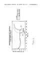
- FIG. 5is an illustrative simulation plot showing wafer temperatures as a function of bias power and time in accordance with the present invention.
- FIG. 6is an optical emission endpoint trace comparing etch times for a high temperature process in accordance with the present invention and a low temperature etch.
- the present inventionrelates to fabrication of integrated circuits, and more particularly to methods of dry etching thin films of “difficult to dry etch” materials such as Platinum, Iridium, Gold, refractory elements, transition elements, their alloys and/or compounds for the formation of structures in an integrated circuit.
- Plasma etchingis presented as a method to pattern or etch difficult to dry etch materials. These materials generally include metals, however other compounds are included which will be described in greater detail below.
- Some examples of etching hard to dry etch materialsinclude platinum or iridium electrodes of stacked capacitors for semiconductor memory devices. Plasma etching of these materials is, however, difficult since these materials do not readily form highly volatile compounds under conventional plasma etch conditions.
- the present inventionprovides a method to plasma etch films of platinum, iridium and other similar materials by using the plasma to heat the wafer to elevated temperatures (e.g., above 200 EC.) and to simultaneously etch the film using halogen including reactive gas mixtures, without using a high temperature (above 200 EC.) wafer electrode.
- the high wafer temperaturesignificantly reduces redeposition of material on the wafer by lowering the sticking probability and, in some cases, increases the volatility of etch by-products.
- the high energy ion bombardment from the plasma and high wafer temperaturefacilitates high etch rates and good etch rate uniformity. Since the wafer electrode is maintained at temperatures of less 100 EC., the present invention is advantageously compatible with other low temperature etch processes such as ARC open and hard mask open in the same chamber.
- the present inventionteaches a method to dry etch thin films of “difficult to dry etch” materials such as Platinum, Iridium, Gold and Copper, refractory elements, transition elements, their alloys and/or compounds.
- the present inventionemploys the plasma to simultaneously perform (a) heating of the wafer to an elevated temperature (e.g., greater than about 200 EC.) and (b) dry/plasma etching of the thin film material.
- a wafer 10is placed in an etch chamber 12 provided in block 100 .
- Etch chamber 12is preferably at about room temperature as is a wafer electrode 14 .
- Wafer 10is placed on wafer electrode 14 that is maintained at a temperature in a temperature range for plasma etching (e.g., less than about 100 EC.).
- the present inventionmay be employed in any plasma reactor in which the plasma is excited using RF or microwave power.
- plasma etchingcharged species from the plasma bombard the surface of wafer 10 and exchange energy with the wafer material which manifests itself in the form of thermal energy (heat).
- heat lossis minimized. This may include minimizing the heat loss from wafer 10 to wafer electrode 14 and to the surroundings by using minimal or zero backside helium cooling and using a very small clamping force on wafer. Other measures may be taken as well.
- a clamp forceis applied by employing chucks 16 to secure wafer 10 in place.
- an electrostatic clampis employed, although a mechanical clamp may be used.
- the clamping forceis set to a very small value, preferably between about 0.1 pounds to about 0 pounds.
- helium pressure on a back side 14 of wafer 10is applied.
- the helium pressure on back side 14 of wafer 10is set to a small value, preferably between about 50 to about 0 Torr.
- Steps 102 and 104ensure minimum loss or transfer of thermal energy from wafer 10 to wafer electrode 14 and to the surroundings. By doing so, most of the energy that is deposited into wafer 10 by the charged species from the plasma (and which is converted to heat) is conserved and therefore results in heating wafer 10 to an elevated temperature in a very short period of time using the charged particle bombardment from the plasma to impart thermal energy to the wafer. Elevated temperatures include temperatures of greater than about 200 EC. and more preferably greater than about 300 EC.
- a reagent gas 18 flow of halogen gasesis supplied to plasma etch chamber 12 .
- the halogen gasespreferably include Fluorine, Chlorine, Bromine and/or Iodine or mixtures thereof.
- An applied RF or microwave field 19 between an electrode 21 and wafer electrode 14disassociates and ionizes gas 18 to form reactive species.
- the reactive species from the plasmareact with thin films or layers 20 formed on wafer 10 .
- layers 20 of difficult to plasma (dry) etch materialse.g., Platinum
- the high wafer temperature along with ion bombardment from the plasmafacilitate the removal of the reaction products from the wafer surface.
- a bias power of etch chamber 12is selected such that the desired high wafer temperature is achieved, by applying RF or microwave power to generate a plasma and applying bias power to wafer electrode 14 to impart high bombardment energy to the ions incident on wafer 10 from the plasma.
- a bias power of between 450 W and about 500 Wmay be employed to achieve temperatures of about 300EC at the surface of wafer 10 .
- Device 30may include a semiconductor memory device, such as a dynamic random access memory (DRAM), a processing chip, an application specific chip or any other semiconductor chip which employs difficult to dry etch materials.
- a layer 32is formed on a substrate 34 .
- Substrate 34may include one or more layers for forming various components for device 30 .
- Layer 32has a mask layer 36 patterned thereon to be employed in patterning layer 32 .
- Layer 32may include Platinum, Iridium, Copper, Gold, transition elements, refractory elements and/or their alloys and compounds.
- Mask layer 36may include one or more of silicon dioxide, silicon nitride, titanium nitride, titanium or other hard mask materials such as Barium Strontium Titanium oxide (BST).
- BSTBarium Strontium Titanium oxide
- device 30is subjected to a plasma etch as described above in accordance with the present invention.
- Exposed portion of layer 32are dry etched to provide structures 38 .
- Structures 38may include conductive lines, interconnects, stacked capacitor electrodes or any other component needed for a particular device design.
- High wafer temperature(e.g. greater than 300 EC.) are achieved without using a high temperature wafer electrode.
- elevated wafer temperatures of greater than about 300 EC.can be achieved using a room temperature (about 25 EC.) electrode.
- FIG. 5an illustrative plot shows experimental data along with simulation results for wafer temperature versus time. The simulation results are shown for different amounts of energy transferred from the plasma to the wafer. These amounts of energy are indicated in the legend of FIG. 5 and have units of mA/cm 2 ⁇ eV.
- the simulationemploys a heat transfer coefficient h equal to 0.002 W/cm 2 ⁇ K and the chuck temperature is 303 K or 30 EC. Wafer surface temperatures at about steady state are indicated to the right of their respective curves.
- a plasma etch reactor used in accordance with the present inventionis therefore compatible with additional etch processes such as ARC (antireflection coating) open etch processes and hard mask open etch processes that operate at wafer temperatures of less than 100 EC.
- ARCantireflection coating
- hard mask open etch processesthat operate at wafer temperatures of less than 100 EC.
- the high wafer temperaturefacilitates etch rate enhancement.
- Platinumis employed to demonstrate the improvements in etch rate for the present invention. Note that the less the endpoint time, the higher the etch rate. As indicated by arrow “A” the etch rate is 30-100% higher, depending on etch conditions than the etch rate indicated for arrow “B”. As indicated in the legend of FIG. 6, a higher temperature provides a shorter end point.
- the present inventionsubstantially increases the end point value by heating the wafer during processing without heating the wafer electrode. In addition, good Pt etch rate uniformity is achieved, for example, within about +/ ⁇ 10%.
- the optical emission endpoint traceemployed light having a wavelength between about 650 nm to about 700 nm. The Platinum was etched using a HBr/O 2 chemistry.
- the present inventionis compatible with a variety of hard mask materials for difficult to dry etch materials including SiO 2 , Si 3 N 4 , TiN, Ti, Barium Strontium Titanium oxide (BST) etc. Experiments performed by the inventors have shown the hard mask remains intact, and there is very little redeposition of the etched materials on features.
- the approach of the present inventionmay be employed to etch other “difficult to plasma (dry) etch” materials such as Iridium, Gold and Copper, refractory elements, transition elements, their alloys and/or compounds.
- the present inventionis particularly useful for patterning Platinum bottom electrodes of stacked capacitors for DRAM chips.
- the present inventionmay be applied industry-wide to etch other materials that do not readily form highly volatile compounds in a plasma such as Copper, Iridium, refractory and transition metals and their alloys.
Landscapes
- Engineering & Computer Science (AREA)
- Chemical & Material Sciences (AREA)
- Physics & Mathematics (AREA)
- Chemical Kinetics & Catalysis (AREA)
- Condensed Matter Physics & Semiconductors (AREA)
- Organic Chemistry (AREA)
- Mechanical Engineering (AREA)
- Plasma & Fusion (AREA)
- Materials Engineering (AREA)
- General Chemical & Material Sciences (AREA)
- Metallurgy (AREA)
- General Physics & Mathematics (AREA)
- Manufacturing & Machinery (AREA)
- Computer Hardware Design (AREA)
- Microelectronics & Electronic Packaging (AREA)
- Power Engineering (AREA)
- Drying Of Semiconductors (AREA)
Abstract
Description
- 1. Technical Field[0001]
- The present invention relates to fabrication of integrated circuits, and in particular to methods of dry etching thin films of “difficult to dry etch” materials such as Platinum, Iridium, Gold, refractory elements, transition elements, their alloys and/or compounds for the formation of structures in an integrated circuit.[0002]
- 2. Description of the Related Art[0003]
- Plasma etching is widely used for the fabrication of microelectronic devices. In plasma etching, a wafer with a desired film to be etched is placed in a plasma environment. The reactive species (neutrals and ionized species) from the plasma react with the wafer surface material to form reaction products. The reaction products are readily removed from the wafer surface due to their highly volatile nature and are pumped away, thereby leading to etching (or removal) of the wafer surface material.[0004]
- The wafer temperature is typically controlled in the less than 100 EC. range in conventional plasma etching, for various technological reasons. This is achieved by placing the wafer on a wafer electrode that is maintained at a desired temperature (e.g., <100 C.). To facilitate the transfer of heat to or from the wafer, Helium gas pressure (or flow) is normally used on the back side of the wafer. The wafer must be clamped to hold the wafer in place during processing, to provide mechanical support to the wafer and to reduce the leakage of the Helium from the backside of the wafer to the plasma environment on the front of the wafer. Clamping is achieved either by mechanical means (using a mechanical clamp) or by using electrostatic force (using a electrostatic clamp or ESC). The wafer electrode is powered using a Bias Power supply to control the energy of ions bombarding the wafer surface.[0005]
- Certain materials such as Platinum, Iridium, Gold and Copper, refractory and transition elements, their alloys and compounds do not dry etch readily in a plasma environment. This is due to the fact that these materials do not form highly volatile compounds under the conditions of conventional plasma etching. For the purpose of the discussion here, such materials are defined as “difficult to dry etch.”[0006]
- Attempts at dry etching these materials using physical etch conditions such as ion beam etching has been shown to result in problems. Due to the low volatility of the etch product species and their associated light sticking probability, significant amount of redeposition occurs leading to critical dimension growth or formation of fence like structures. Halogen containing volatile compounds of Platinum, Iridium, Gold and Copper, refractory and transition elements, their alloys can be formed in absence of a plasma in a purely chemical reaction at very high temperatures (for example >600 EC.). However, the use of heated wafer electrodes to heat the wafer to an elevated temperature (>200 EC.) has many disadvantages. Some of these disadvantages include the following:[0007]
- (1) Since heated wafer electrodes are typically designed for elevated temperature (>200 EC.) service, the electrodes cannot be readily cooled down to conventional processing temperatures (<100 EC.) in a short period of time (such as for use within a process recipe). As a result, a plasma etch chamber equipped with a heated wafer electrode is not compatible with other lower temperature (<100 EC.) processes such as ARC open etch and hard mask open etch. A separate chamber must therefore be used for any additional etch processes that operate at conventional wafer temperatures.[0008]
- (2) The materials of construction for the heated electrode must be chosen very carefully to be compatible with a high vacuum plasma reaction chamber. Thermal isolation of the electrode must be achieved in addition to electrical isolation from other parts of the tool. Due to the stringent design and operation requirements of the speciality materials, the electrodes tend to be expensive and add to the cost of the tool. In addition, an electrode that is heated to elevated temperatures of >200 EC. requires additional safety precautions and cool-down times for maintenance.[0009]
- (3) Clamping and de-clamping reliability may be an issue for electrodes operating at elevated temperatures, especially for electrostatic clamps.[0010]
- Therefore, a need exists for a method for dry etching “difficult to dry etch” materials which employs electrode temperatures of less than about 100 EC. for an electrode equipped plasma etch chamber. A further need exists for a method for achieving high wafer temperature for dry etch processing of “difficult to dry etch” materials.[0011]
- A method for etching material which does not readily form volatile compounds in a plasma, in accordance with the present invention, includes providing a plasma etch chamber including a wafer electrode at an initial temperature. The wafer electrode supports a wafer, and the wafer includes a layer of the material which does not readily form volatile compounds in plasma. The wafer is bombarded with charged particles from a plasma generated in the plasma etch chamber to impart thermal energy to the wafer. A reactive gas flow is provided to react with etch products of the material. Bias power is applied to the wafer electrode to impart bombardment energy to the charged particles incident on the wafer from the plasma such that a predetermined temperature is generated on a surface of the wafer wherein the wafer electrode is maintained at about the initial temperature.[0012]
- In other methods, the step of applying bias power to the wafer electrode may include the step of selecting the bias power to reach a predetermined temperature on the wafer of greater than 200 degrees Celsius. The method may further include the step of reducing heat loss from the wafer to the wafer electrode and to wafer surroundings. The step of reducing heat loss may include the step of substantially eliminating backside cooling of the wafer and/or reducing a clamping force to between about 0.1 pounds to about 0.0 pounds between the wafer and the wafer electrode. The initial temperature may be about room temperature. The predetermined temperature may be greater than about 300 degrees Celsius. The method may further include the step of etching the material to form interconnect structures in an integrated circuit. The step of etching the material to form capacitor electrodes in an integrated circuit may be included. The material may include at least one of Platinum, Iridium, Gold, Copper, a refractory element and a transition element. The step of providing a reactive gas flow may include the step of providing the reactive gas flow with halogens.[0013]
- A method for plasma etching a layer of at least one of Platinum, Iridium, Gold, Copper, a refractory element and a transition element, in accordance with the present invention, includes forming a hard mask on the layer for providing an etch pattern on the layer, the layer being formed on a wafer, providing a plasma etch chamber including a wafer electrode at an initial temperature, securing the wafer to the wafer electrode with a clamping force of substantially zero, bombarding the wafer with charged particles from a plasma generated in the plasma etch chamber to impart thermal energy to the wafer, providing a reactive gas flow including halogens to react with the layer to form etch products of the layer and applying bias power to the wafer electrode to impart bombardment energy to the charged particles incident on the wafer from the plasma such that a predetermined temperature is generated on a surface of the wafer while the wafer electrode is maintained at about the initial temperature, the predetermined temperature having a value sufficient to make the etch products volatile to react with the reactive gas flow.[0014]
- In other methods, the step of applying bias power to the wafer electrode may include the step of selecting the bias power to reach a predetermined temperature on the wafer of greater than 200 degrees Celsius. The step of reducing heat loss from the wafer to the wafer electrode and to wafer surroundings by substantially eliminating backside cooling of the wafer may be included. The clamping force may be between about 0.1 pounds to about 0.0 pounds between the wafer and the wafer electrode. The initial temperature may be about room temperature. The method may further include the step of etching the layer to form interconnect structures in an integrated circuit. The method may further include the step of etching the layer to form capacitor electrodes in an integrated circuit.[0015]
- A method for patterning platinum electrodes for stacked capacitors for dynamic random access memory chips, in accordance with the present invention, includes providing a wafer having a layer of Platinum formed thereon, patterning a hard mask on the layer of Platinum, securing the wafer to a wafer electrode in a plasma etch chamber, the wafer electrode being at an initial temperature, bombarding the wafer with charged particles from a plasma generated in the plasma etch chamber to impart thermal energy to the wafer, providing a reactive gas flow to react to form etch products of the Platinum and to etch the Platinum in accordance with the hard mask, and applying bias power to the wafer electrode to impart bombardment energy to the charged particles incident on the wafer from the plasma such that a temperature of greater than about 200 degrees Celsius is generated on a surface of the wafer wherein the wafer electrode is maintained at about the initial temperature.[0016]
- In other methods, the step of reducing heat loss from the wafer to the wafer electrode and to wafer surroundings by substantially eliminating backside cooling of the wafer may be included. The step of securing the wafer to a wafer electrode may include the step of clamping the wafer to the wafer electrodes with a clamping force between about 0.1 pounds to about 0.0 pounds. The initial temperature may be about room temperature. The hard mask may include Barium Strontium Titanium oxide (BST). The reagent gas preferably includes halogens.[0017]
- These and other objects, features and advantages of the present invention will become apparent from the following detailed description of illustrative embodiments thereof, which is to be read in connection with the accompanying drawings.[0018]
- This disclosure will present in detail the following description of preferred embodiments with reference to the following figures wherein:[0019]
- FIG. 1 is a block diagram of showing a plasma etch chamber employed in accordance with the present invention;[0020]
- FIG. 2 is a flow diagram of one method for etching “difficult to plasma (dry) etch” materials in accordance with the present invention;[0021]
- FIG. 3 is a cross-sectional view of a semiconductor device showing a hard mask patterned on a “difficult to plasma (dry) etch” material for processing in accordance with the present invention;[0022]
- FIG. 4 is a cross-sectional view of the semiconductor device of FIG. 3 showing the “difficult to plasma (dry) etch” material plasma (dry) etched in accordance with the present invention;[0023]
- FIG. 5 is an illustrative simulation plot showing wafer temperatures as a function of bias power and time in accordance with the present invention; and[0024]
- FIG. 6 is an optical emission endpoint trace comparing etch times for a high temperature process in accordance with the present invention and a low temperature etch.[0025]
- The present invention relates to fabrication of integrated circuits, and more particularly to methods of dry etching thin films of “difficult to dry etch” materials such as Platinum, Iridium, Gold, refractory elements, transition elements, their alloys and/or compounds for the formation of structures in an integrated circuit. Plasma etching is presented as a method to pattern or etch difficult to dry etch materials. These materials generally include metals, however other compounds are included which will be described in greater detail below. Some examples of etching hard to dry etch materials include platinum or iridium electrodes of stacked capacitors for semiconductor memory devices. Plasma etching of these materials is, however, difficult since these materials do not readily form highly volatile compounds under conventional plasma etch conditions.[0026]
- The present invention provides a method to plasma etch films of platinum, iridium and other similar materials by using the plasma to heat the wafer to elevated temperatures (e.g., above 200 EC.) and to simultaneously etch the film using halogen including reactive gas mixtures, without using a high temperature (above 200 EC.) wafer electrode. The high wafer temperature significantly reduces redeposition of material on the wafer by lowering the sticking probability and, in some cases, increases the volatility of etch by-products. The high energy ion bombardment from the plasma and high wafer temperature facilitates high etch rates and good etch rate uniformity. Since the wafer electrode is maintained at temperatures of less 100 EC., the present invention is advantageously compatible with other low temperature etch processes such as ARC open and hard mask open in the same chamber.[0027]
- The present invention teaches a method to dry etch thin films of “difficult to dry etch” materials such as Platinum, Iridium, Gold and Copper, refractory elements, transition elements, their alloys and/or compounds. The present invention employs the plasma to simultaneously perform (a) heating of the wafer to an elevated temperature (e.g., greater than about 200 EC.) and (b) dry/plasma etching of the thin film material.[0028]
- Referring now in specific detail to the drawings in which like reference numerals identify similar or identical elements throughout the several views, and initially to FIGS. 1 and 2, a[0029]
wafer 10 is placed in anetch chamber 12 provided inblock 100.Etch chamber 12 is preferably at about room temperature as is awafer electrode 14.Wafer 10 is placed onwafer electrode 14 that is maintained at a temperature in a temperature range for plasma etching (e.g., less than about 100 EC.). - The present invention may be employed in any plasma reactor in which the plasma is excited using RF or microwave power. During plasma etching, charged species from the plasma bombard the surface of[0030]
wafer 10 and exchange energy with the wafer material which manifests itself in the form of thermal energy (heat). Inblock 103, heat loss is minimized. This may include minimizing the heat loss fromwafer 10 towafer electrode 14 and to the surroundings by using minimal or zero backside helium cooling and using a very small clamping force on wafer. Other measures may be taken as well. Inblock 102, a clamp force is applied by employingchucks 16 to securewafer 10 in place. In a preferred embodiment, an electrostatic clamp is employed, although a mechanical clamp may be used. The clamping force is set to a very small value, preferably between about 0.1 pounds to about 0 pounds. Inblock 104, helium pressure on aback side 14 ofwafer 10 is applied. In a preferred embodiment, the helium pressure onback side 14 ofwafer 10 is set to a small value, preferably between about 50 to about 0 Torr.Steps wafer 10 towafer electrode 14 and to the surroundings. By doing so, most of the energy that is deposited intowafer 10 by the charged species from the plasma (and which is converted to heat) is conserved and therefore results inheating wafer 10 to an elevated temperature in a very short period of time using the charged particle bombardment from the plasma to impart thermal energy to the wafer. Elevated temperatures include temperatures of greater than about 200 EC. and more preferably greater than about 300 EC. - In[0031]
block 106, a reagent gas18 flow of halogen gases is supplied toplasma etch chamber 12. The halogen gases preferably include Fluorine, Chlorine, Bromine and/or Iodine or mixtures thereof. An applied RF or microwave field19 between an electrode21 andwafer electrode 14 disassociates and ionizes gas18 to form reactive species. The reactive species from the plasma react with thin films or layers20 formed onwafer 10. Inblock 108, layers20 of difficult to plasma (dry) etch materials (e.g., Platinum) form reaction products (a thin layer of halogenated material). The high wafer temperature along with ion bombardment from the plasma facilitate the removal of the reaction products from the wafer surface. Due to the high wafer temperature, the sticking probability on the wafer surface is reduced significantly, thus reducing or eliminating completely residue or fence build-up. The high wafer temperature also facilitates high etch rate oflayers 20. Advantageously,layer 20 is dry etched without etch products building up while maintaining alow wafer electrode 14 temperature. Inblock 110, a bias power ofetch chamber 12 is selected such that the desired high wafer temperature is achieved, by applying RF or microwave power to generate a plasma and applying bias power towafer electrode 14 to impart high bombardment energy to the ions incident onwafer 10 from the plasma. For example, a bias power of between 450 W and about 500 W may be employed to achieve temperatures of about 300EC at the surface ofwafer 10. - Referring to FIG. 3, an illustrative cross-sectional view of a[0032]
semiconductor device 30 is shown.Device 30 may include a semiconductor memory device, such as a dynamic random access memory (DRAM), a processing chip, an application specific chip or any other semiconductor chip which employs difficult to dry etch materials. Alayer 32 is formed on asubstrate 34.Substrate 34 may include one or more layers for forming various components fordevice 30.Layer 32 has amask layer 36 patterned thereon to be employed inpatterning layer 32.Layer 32 may include Platinum, Iridium, Copper, Gold, transition elements, refractory elements and/or their alloys and compounds.Mask layer 36 may include one or more of silicon dioxide, silicon nitride, titanium nitride, titanium or other hard mask materials such as Barium Strontium Titanium oxide (BST). - Referring to FIG. 4,[0033]
device 30 is subjected to a plasma etch as described above in accordance with the present invention. Exposed portion oflayer 32 are dry etched to providestructures 38.Structures 38 may include conductive lines, interconnects, stacked capacitor electrodes or any other component needed for a particular device design. - Some of the advantages of the present invention include the following:[0034]
- (1) High wafer temperature (e.g. greater than 300 EC.) are achieved without using a high temperature wafer electrode. In fact, elevated wafer temperatures of greater than about 300 EC. can be achieved using a room temperature (about 25 EC.) electrode. Referring to FIG. 5, an illustrative plot shows experimental data along with simulation results for wafer temperature versus time. The simulation results are shown for different amounts of energy transferred from the plasma to the wafer. These amounts of energy are indicated in the legend of FIG. 5 and have units of mA/cm[0035]2−eV. The simulation employs a heat transfer coefficient h equal to 0.002 W/cm2−K and the chuck temperature is 303 K or 30 EC. Wafer surface temperatures at about steady state are indicated to the right of their respective curves.
- A plasma etch reactor used in accordance with the present invention is therefore compatible with additional etch processes such as ARC (antireflection coating) open etch processes and hard mask open etch processes that operate at wafer temperatures of less than 100 EC.[0036]
- (2) The high wafer temperature facilitates etch rate enhancement. In the illustrative optical endpoint trace of FIG. 6, Platinum is employed to demonstrate the improvements in etch rate for the present invention. Note that the less the endpoint time, the higher the etch rate. As indicated by arrow “A” the etch rate is 30-100% higher, depending on etch conditions than the etch rate indicated for arrow “B”. As indicated in the legend of FIG. 6, a higher temperature provides a shorter end point. The present invention substantially increases the end point value by heating the wafer during processing without heating the wafer electrode. In addition, good Pt etch rate uniformity is achieved, for example, within about +/−10%. The optical emission endpoint trace employed light having a wavelength between about 650 nm to about 700 nm. The Platinum was etched using a HBr/O[0037]2chemistry.
- (3) The present invention is compatible with a variety of hard mask materials for difficult to dry etch materials including SiO[0038]2, Si3N4, TiN, Ti, Barium Strontium Titanium oxide (BST) etc. Experiments performed by the inventors have shown the hard mask remains intact, and there is very little redeposition of the etched materials on features.
- (4) The high wafer temperature achieved using the present invention decreases sticking probability of reaction products thereby reducing the amount of redeposited material on the sidewalls of the etched feature.[0039]
- (5) The approach of the present invention may be employed to etch other “difficult to plasma (dry) etch” materials such as Iridium, Gold and Copper, refractory elements, transition elements, their alloys and/or compounds.[0040]
- The present invention is particularly useful for patterning Platinum bottom electrodes of stacked capacitors for DRAM chips. However, the present invention may be applied industry-wide to etch other materials that do not readily form highly volatile compounds in a plasma such as Copper, Iridium, refractory and transition metals and their alloys.[0041]
- Having described preferred embodiments for a method of plasma etching thin films of difficult to dry etch materials (which are intended to be illustrative and not limiting), it is noted that modifications and variations can be made by persons skilled in the art in light of the above teachings. It is therefore to be understood that changes may be made in the particular embodiments of the invention disclosed which are within the scope and spirit of the invention as outlined by the appended claims. Having thus described the invention with the details and particularity required by the patent laws, what is claimed and desired protected by Letters Patent is set forth in the appended claims.[0042]
Claims (24)
Priority Applications (3)
| Application Number | Priority Date | Filing Date | Title |
|---|---|---|---|
| US09/396,178US6548414B2 (en) | 1999-09-14 | 1999-09-14 | Method of plasma etching thin films of difficult to dry etch materials |
| PCT/US2000/023097WO2001020655A1 (en) | 1999-09-14 | 2000-08-24 | Method of plasma etching thin films of difficult to dry etch materials |
| TW089117625ATW478065B (en) | 1999-09-14 | 2000-08-30 | Method of plasma etching thin films of difficult to dry etch materials |
Applications Claiming Priority (1)
| Application Number | Priority Date | Filing Date | Title |
|---|---|---|---|
| US09/396,178US6548414B2 (en) | 1999-09-14 | 1999-09-14 | Method of plasma etching thin films of difficult to dry etch materials |
Publications (2)
| Publication Number | Publication Date |
|---|---|
| US20010053610A1true US20010053610A1 (en) | 2001-12-20 |
| US6548414B2 US6548414B2 (en) | 2003-04-15 |
Family
ID=23566179
Family Applications (1)
| Application Number | Title | Priority Date | Filing Date |
|---|---|---|---|
| US09/396,178Expired - LifetimeUS6548414B2 (en) | 1999-09-14 | 1999-09-14 | Method of plasma etching thin films of difficult to dry etch materials |
Country Status (3)
| Country | Link |
|---|---|
| US (1) | US6548414B2 (en) |
| TW (1) | TW478065B (en) |
| WO (1) | WO2001020655A1 (en) |
Cited By (125)
| Publication number | Priority date | Publication date | Assignee | Title |
|---|---|---|---|---|
| US20030162401A1 (en)* | 2002-02-28 | 2003-08-28 | Fujitsu Limited | Semiconductor device manufacturing method |
| US6692648B2 (en)* | 2000-12-22 | 2004-02-17 | Applied Materials Inc. | Method of plasma heating and etching a substrate |
| US20040042134A1 (en)* | 2002-09-04 | 2004-03-04 | Kim Ki-Nam | Methods for forming electronic devices including capacitor structures |
| US6709609B2 (en)* | 2000-12-22 | 2004-03-23 | Applied Materials Inc. | Plasma heating of a substrate with subsequent high temperature etching |
| US20060108323A1 (en)* | 2003-06-30 | 2006-05-25 | Shuichi Okawa | Dry etching method |
| US20090181545A1 (en)* | 2004-06-23 | 2009-07-16 | Nobuyuki Negishi | Dry-etching method and apparatus |
| US20110156012A1 (en)* | 2009-11-12 | 2011-06-30 | Sony Corporation | Double layer hardmask for organic devices |
| US20150014152A1 (en)* | 2013-07-12 | 2015-01-15 | International Business Machines Corporation | Selective sputtering for pattern transfer |
| US9349605B1 (en) | 2015-08-07 | 2016-05-24 | Applied Materials, Inc. | Oxide etch selectivity systems and methods |
| US9368364B2 (en) | 2014-09-24 | 2016-06-14 | Applied Materials, Inc. | Silicon etch process with tunable selectivity to SiO2 and other materials |
| US9373522B1 (en) | 2015-01-22 | 2016-06-21 | Applied Mateials, Inc. | Titanium nitride removal |
| US9373517B2 (en) | 2012-08-02 | 2016-06-21 | Applied Materials, Inc. | Semiconductor processing with DC assisted RF power for improved control |
| US9378969B2 (en) | 2014-06-19 | 2016-06-28 | Applied Materials, Inc. | Low temperature gas-phase carbon removal |
| US9378978B2 (en) | 2014-07-31 | 2016-06-28 | Applied Materials, Inc. | Integrated oxide recess and floating gate fin trimming |
| US9385028B2 (en) | 2014-02-03 | 2016-07-05 | Applied Materials, Inc. | Air gap process |
| US9384997B2 (en) | 2012-11-20 | 2016-07-05 | Applied Materials, Inc. | Dry-etch selectivity |
| US9390937B2 (en) | 2012-09-20 | 2016-07-12 | Applied Materials, Inc. | Silicon-carbon-nitride selective etch |
| US9396989B2 (en) | 2014-01-27 | 2016-07-19 | Applied Materials, Inc. | Air gaps between copper lines |
| US9406523B2 (en) | 2014-06-19 | 2016-08-02 | Applied Materials, Inc. | Highly selective doped oxide removal method |
| US9412608B2 (en) | 2012-11-30 | 2016-08-09 | Applied Materials, Inc. | Dry-etch for selective tungsten removal |
| US9418858B2 (en) | 2011-10-07 | 2016-08-16 | Applied Materials, Inc. | Selective etch of silicon by way of metastable hydrogen termination |
| US9425058B2 (en) | 2014-07-24 | 2016-08-23 | Applied Materials, Inc. | Simplified litho-etch-litho-etch process |
| US9437451B2 (en) | 2012-09-18 | 2016-09-06 | Applied Materials, Inc. | Radical-component oxide etch |
| US9449845B2 (en) | 2012-12-21 | 2016-09-20 | Applied Materials, Inc. | Selective titanium nitride etching |
| US9449846B2 (en) | 2015-01-28 | 2016-09-20 | Applied Materials, Inc. | Vertical gate separation |
| US9472412B2 (en) | 2013-12-02 | 2016-10-18 | Applied Materials, Inc. | Procedure for etch rate consistency |
| US9472417B2 (en) | 2013-11-12 | 2016-10-18 | Applied Materials, Inc. | Plasma-free metal etch |
| US9478432B2 (en) | 2014-09-25 | 2016-10-25 | Applied Materials, Inc. | Silicon oxide selective removal |
| US9478434B2 (en) | 2014-09-24 | 2016-10-25 | Applied Materials, Inc. | Chlorine-based hardmask removal |
| US9496167B2 (en) | 2014-07-31 | 2016-11-15 | Applied Materials, Inc. | Integrated bit-line airgap formation and gate stack post clean |
| US9502258B2 (en) | 2014-12-23 | 2016-11-22 | Applied Materials, Inc. | Anisotropic gap etch |
| US9499898B2 (en) | 2014-03-03 | 2016-11-22 | Applied Materials, Inc. | Layered thin film heater and method of fabrication |
| US9553102B2 (en) | 2014-08-19 | 2017-01-24 | Applied Materials, Inc. | Tungsten separation |
| US9564296B2 (en) | 2014-03-20 | 2017-02-07 | Applied Materials, Inc. | Radial waveguide systems and methods for post-match control of microwaves |
| US9576809B2 (en) | 2013-11-04 | 2017-02-21 | Applied Materials, Inc. | Etch suppression with germanium |
| US9607856B2 (en) | 2013-03-05 | 2017-03-28 | Applied Materials, Inc. | Selective titanium nitride removal |
| US9659792B2 (en) | 2013-03-15 | 2017-05-23 | Applied Materials, Inc. | Processing systems and methods for halide scavenging |
| US9659753B2 (en) | 2014-08-07 | 2017-05-23 | Applied Materials, Inc. | Grooved insulator to reduce leakage current |
| US9691645B2 (en) | 2015-08-06 | 2017-06-27 | Applied Materials, Inc. | Bolted wafer chuck thermal management systems and methods for wafer processing systems |
| US9721789B1 (en) | 2016-10-04 | 2017-08-01 | Applied Materials, Inc. | Saving ion-damaged spacers |
| US9728437B2 (en) | 2015-02-03 | 2017-08-08 | Applied Materials, Inc. | High temperature chuck for plasma processing systems |
| US9741593B2 (en) | 2015-08-06 | 2017-08-22 | Applied Materials, Inc. | Thermal management systems and methods for wafer processing systems |
| US9754800B2 (en) | 2010-05-27 | 2017-09-05 | Applied Materials, Inc. | Selective etch for silicon films |
| US9768034B1 (en) | 2016-11-11 | 2017-09-19 | Applied Materials, Inc. | Removal methods for high aspect ratio structures |
| US9773648B2 (en) | 2013-08-30 | 2017-09-26 | Applied Materials, Inc. | Dual discharge modes operation for remote plasma |
| US9842744B2 (en) | 2011-03-14 | 2017-12-12 | Applied Materials, Inc. | Methods for etch of SiN films |
| US9865484B1 (en) | 2016-06-29 | 2018-01-09 | Applied Materials, Inc. | Selective etch using material modification and RF pulsing |
| US9881805B2 (en) | 2015-03-02 | 2018-01-30 | Applied Materials, Inc. | Silicon selective removal |
| US9885117B2 (en) | 2014-03-31 | 2018-02-06 | Applied Materials, Inc. | Conditioned semiconductor system parts |
| US9934942B1 (en) | 2016-10-04 | 2018-04-03 | Applied Materials, Inc. | Chamber with flow-through source |
| US9947549B1 (en) | 2016-10-10 | 2018-04-17 | Applied Materials, Inc. | Cobalt-containing material removal |
| US9966240B2 (en) | 2014-10-14 | 2018-05-08 | Applied Materials, Inc. | Systems and methods for internal surface conditioning assessment in plasma processing equipment |
| US9978564B2 (en) | 2012-09-21 | 2018-05-22 | Applied Materials, Inc. | Chemical control features in wafer process equipment |
| US10026621B2 (en) | 2016-11-14 | 2018-07-17 | Applied Materials, Inc. | SiN spacer profile patterning |
| US10043674B1 (en) | 2017-08-04 | 2018-08-07 | Applied Materials, Inc. | Germanium etching systems and methods |
| US10043684B1 (en) | 2017-02-06 | 2018-08-07 | Applied Materials, Inc. | Self-limiting atomic thermal etching systems and methods |
| US10049891B1 (en) | 2017-05-31 | 2018-08-14 | Applied Materials, Inc. | Selective in situ cobalt residue removal |
| US10062587B2 (en) | 2012-07-18 | 2018-08-28 | Applied Materials, Inc. | Pedestal with multi-zone temperature control and multiple purge capabilities |
| US10062579B2 (en) | 2016-10-07 | 2018-08-28 | Applied Materials, Inc. | Selective SiN lateral recess |
| US10062578B2 (en) | 2011-03-14 | 2018-08-28 | Applied Materials, Inc. | Methods for etch of metal and metal-oxide films |
| US10062575B2 (en) | 2016-09-09 | 2018-08-28 | Applied Materials, Inc. | Poly directional etch by oxidation |
| US10062585B2 (en) | 2016-10-04 | 2018-08-28 | Applied Materials, Inc. | Oxygen compatible plasma source |
| US10128086B1 (en) | 2017-10-24 | 2018-11-13 | Applied Materials, Inc. | Silicon pretreatment for nitride removal |
| US10163696B2 (en) | 2016-11-11 | 2018-12-25 | Applied Materials, Inc. | Selective cobalt removal for bottom up gapfill |
| US10170336B1 (en) | 2017-08-04 | 2019-01-01 | Applied Materials, Inc. | Methods for anisotropic control of selective silicon removal |
| US10224210B2 (en) | 2014-12-09 | 2019-03-05 | Applied Materials, Inc. | Plasma processing system with direct outlet toroidal plasma source |
| US10242908B2 (en) | 2016-11-14 | 2019-03-26 | Applied Materials, Inc. | Airgap formation with damage-free copper |
| US10256112B1 (en) | 2017-12-08 | 2019-04-09 | Applied Materials, Inc. | Selective tungsten removal |
| US10256079B2 (en) | 2013-02-08 | 2019-04-09 | Applied Materials, Inc. | Semiconductor processing systems having multiple plasma configurations |
| US10283321B2 (en) | 2011-01-18 | 2019-05-07 | Applied Materials, Inc. | Semiconductor processing system and methods using capacitively coupled plasma |
| US10283324B1 (en) | 2017-10-24 | 2019-05-07 | Applied Materials, Inc. | Oxygen treatment for nitride etching |
| US10297458B2 (en) | 2017-08-07 | 2019-05-21 | Applied Materials, Inc. | Process window widening using coated parts in plasma etch processes |
| US10319739B2 (en) | 2017-02-08 | 2019-06-11 | Applied Materials, Inc. | Accommodating imperfectly aligned memory holes |
| US10319600B1 (en) | 2018-03-12 | 2019-06-11 | Applied Materials, Inc. | Thermal silicon etch |
| US10319649B2 (en) | 2017-04-11 | 2019-06-11 | Applied Materials, Inc. | Optical emission spectroscopy (OES) for remote plasma monitoring |
| US10354889B2 (en) | 2017-07-17 | 2019-07-16 | Applied Materials, Inc. | Non-halogen etching of silicon-containing materials |
| US10403507B2 (en) | 2017-02-03 | 2019-09-03 | Applied Materials, Inc. | Shaped etch profile with oxidation |
| US10424485B2 (en) | 2013-03-01 | 2019-09-24 | Applied Materials, Inc. | Enhanced etching processes using remote plasma sources |
| US10431429B2 (en) | 2017-02-03 | 2019-10-01 | Applied Materials, Inc. | Systems and methods for radial and azimuthal control of plasma uniformity |
| US10468267B2 (en) | 2017-05-31 | 2019-11-05 | Applied Materials, Inc. | Water-free etching methods |
| US10465294B2 (en) | 2014-05-28 | 2019-11-05 | Applied Materials, Inc. | Oxide and metal removal |
| US10490406B2 (en) | 2018-04-10 | 2019-11-26 | Appled Materials, Inc. | Systems and methods for material breakthrough |
| US10497573B2 (en) | 2018-03-13 | 2019-12-03 | Applied Materials, Inc. | Selective atomic layer etching of semiconductor materials |
| US10504754B2 (en) | 2016-05-19 | 2019-12-10 | Applied Materials, Inc. | Systems and methods for improved semiconductor etching and component protection |
| US10504700B2 (en) | 2015-08-27 | 2019-12-10 | Applied Materials, Inc. | Plasma etching systems and methods with secondary plasma injection |
| US10522371B2 (en) | 2016-05-19 | 2019-12-31 | Applied Materials, Inc. | Systems and methods for improved semiconductor etching and component protection |
| US10541184B2 (en) | 2017-07-11 | 2020-01-21 | Applied Materials, Inc. | Optical emission spectroscopic techniques for monitoring etching |
| US10541246B2 (en) | 2017-06-26 | 2020-01-21 | Applied Materials, Inc. | 3D flash memory cells which discourage cross-cell electrical tunneling |
| US10546729B2 (en) | 2016-10-04 | 2020-01-28 | Applied Materials, Inc. | Dual-channel showerhead with improved profile |
| US10566206B2 (en) | 2016-12-27 | 2020-02-18 | Applied Materials, Inc. | Systems and methods for anisotropic material breakthrough |
| US10573527B2 (en) | 2018-04-06 | 2020-02-25 | Applied Materials, Inc. | Gas-phase selective etching systems and methods |
| US10573496B2 (en) | 2014-12-09 | 2020-02-25 | Applied Materials, Inc. | Direct outlet toroidal plasma source |
| US10593560B2 (en) | 2018-03-01 | 2020-03-17 | Applied Materials, Inc. | Magnetic induction plasma source for semiconductor processes and equipment |
| US10593523B2 (en) | 2014-10-14 | 2020-03-17 | Applied Materials, Inc. | Systems and methods for internal surface conditioning in plasma processing equipment |
| US10615047B2 (en) | 2018-02-28 | 2020-04-07 | Applied Materials, Inc. | Systems and methods to form airgaps |
| US10629473B2 (en) | 2016-09-09 | 2020-04-21 | Applied Materials, Inc. | Footing removal for nitride spacer |
| US10672642B2 (en) | 2018-07-24 | 2020-06-02 | Applied Materials, Inc. | Systems and methods for pedestal configuration |
| US10679870B2 (en) | 2018-02-15 | 2020-06-09 | Applied Materials, Inc. | Semiconductor processing chamber multistage mixing apparatus |
| US10699879B2 (en) | 2018-04-17 | 2020-06-30 | Applied Materials, Inc. | Two piece electrode assembly with gap for plasma control |
| US10727080B2 (en) | 2017-07-07 | 2020-07-28 | Applied Materials, Inc. | Tantalum-containing material removal |
| US10755941B2 (en) | 2018-07-06 | 2020-08-25 | Applied Materials, Inc. | Self-limiting selective etching systems and methods |
| US10854426B2 (en) | 2018-01-08 | 2020-12-01 | Applied Materials, Inc. | Metal recess for semiconductor structures |
| US10872778B2 (en) | 2018-07-06 | 2020-12-22 | Applied Materials, Inc. | Systems and methods utilizing solid-phase etchants |
| US10886137B2 (en) | 2018-04-30 | 2021-01-05 | Applied Materials, Inc. | Selective nitride removal |
| US10892198B2 (en) | 2018-09-14 | 2021-01-12 | Applied Materials, Inc. | Systems and methods for improved performance in semiconductor processing |
| US10903054B2 (en) | 2017-12-19 | 2021-01-26 | Applied Materials, Inc. | Multi-zone gas distribution systems and methods |
| US10920319B2 (en) | 2019-01-11 | 2021-02-16 | Applied Materials, Inc. | Ceramic showerheads with conductive electrodes |
| US10920320B2 (en) | 2017-06-16 | 2021-02-16 | Applied Materials, Inc. | Plasma health determination in semiconductor substrate processing reactors |
| US10943834B2 (en) | 2017-03-13 | 2021-03-09 | Applied Materials, Inc. | Replacement contact process |
| US10964512B2 (en) | 2018-02-15 | 2021-03-30 | Applied Materials, Inc. | Semiconductor processing chamber multistage mixing apparatus and methods |
| US11049755B2 (en) | 2018-09-14 | 2021-06-29 | Applied Materials, Inc. | Semiconductor substrate supports with embedded RF shield |
| US11062887B2 (en) | 2018-09-17 | 2021-07-13 | Applied Materials, Inc. | High temperature RF heater pedestals |
| US11121002B2 (en) | 2018-10-24 | 2021-09-14 | Applied Materials, Inc. | Systems and methods for etching metals and metal derivatives |
| CN113643973A (en)* | 2020-04-27 | 2021-11-12 | 中微半导体设备(上海)股份有限公司 | Method and device for low temperature etching |
| US11239061B2 (en) | 2014-11-26 | 2022-02-01 | Applied Materials, Inc. | Methods and systems to enhance process uniformity |
| US11257693B2 (en) | 2015-01-09 | 2022-02-22 | Applied Materials, Inc. | Methods and systems to improve pedestal temperature control |
| US11276559B2 (en) | 2017-05-17 | 2022-03-15 | Applied Materials, Inc. | Semiconductor processing chamber for multiple precursor flow |
| US11276590B2 (en) | 2017-05-17 | 2022-03-15 | Applied Materials, Inc. | Multi-zone semiconductor substrate supports |
| US11328909B2 (en) | 2017-12-22 | 2022-05-10 | Applied Materials, Inc. | Chamber conditioning and removal processes |
| US11417534B2 (en) | 2018-09-21 | 2022-08-16 | Applied Materials, Inc. | Selective material removal |
| US11437242B2 (en) | 2018-11-27 | 2022-09-06 | Applied Materials, Inc. | Selective removal of silicon-containing materials |
| US11594428B2 (en) | 2015-02-03 | 2023-02-28 | Applied Materials, Inc. | Low temperature chuck for plasma processing systems |
| US11682560B2 (en) | 2018-10-11 | 2023-06-20 | Applied Materials, Inc. | Systems and methods for hafnium-containing film removal |
| US11721527B2 (en) | 2019-01-07 | 2023-08-08 | Applied Materials, Inc. | Processing chamber mixing systems |
| US12340979B2 (en) | 2017-05-17 | 2025-06-24 | Applied Materials, Inc. | Semiconductor processing chamber for improved precursor flow |
Families Citing this family (7)
| Publication number | Priority date | Publication date | Assignee | Title |
|---|---|---|---|---|
| US6541361B2 (en)* | 2001-06-27 | 2003-04-01 | Lam Research Corp. | Plasma enhanced method for increasing silicon-containing photoresist selectivity |
| US6728591B1 (en)* | 2001-08-01 | 2004-04-27 | Advanced Micro Devices, Inc. | Method and apparatus for run-to-run control of trench profiles |
| TWI278532B (en)* | 2002-06-23 | 2007-04-11 | Asml Us Inc | Method for energy-assisted atomic layer deposition and removal |
| US20050109276A1 (en)* | 2003-11-25 | 2005-05-26 | Applied Materials, Inc. | Thermal chemical vapor deposition of silicon nitride using BTBAS bis(tertiary-butylamino silane) in a single wafer chamber |
| US20060025049A1 (en)* | 2004-07-30 | 2006-02-02 | Applied Materials, Inc. | Spray slurry delivery system for polish performance improvement and cost reduction |
| US20070082507A1 (en)* | 2005-10-06 | 2007-04-12 | Applied Materials, Inc. | Method and apparatus for the low temperature deposition of doped silicon nitride films |
| US20080145536A1 (en)* | 2006-12-13 | 2008-06-19 | Applied Materials, Inc. | METHOD AND APPARATUS FOR LOW TEMPERATURE AND LOW K SiBN DEPOSITION |
Family Cites Families (9)
| Publication number | Priority date | Publication date | Assignee | Title |
|---|---|---|---|---|
| JP3122579B2 (en)* | 1994-07-27 | 2001-01-09 | シャープ株式会社 | Pt film etching method |
| KR0175017B1 (en)* | 1995-10-23 | 1999-04-01 | 윤종용 | Etching method using alumina forming apparatus and alumina mask |
| US5914851A (en)* | 1995-12-22 | 1999-06-22 | International Business Machines Corporation | Isolated sidewall capacitor |
| US6008139A (en)* | 1996-06-17 | 1999-12-28 | Applied Materials Inc. | Method of etching polycide structures |
| WO1998000859A1 (en)* | 1996-07-03 | 1998-01-08 | Tegal Corporation | Method and apparatus for etching a semiconductor wafer |
| US6010603A (en)* | 1997-07-09 | 2000-01-04 | Applied Materials, Inc. | Patterned copper etch for micron and submicron features, using enhanced physical bombardment |
| US6008140A (en)* | 1997-08-13 | 1999-12-28 | Applied Materials, Inc. | Copper etch using HCI and HBr chemistry |
| JP2003526191A (en)* | 1997-08-13 | 2003-09-02 | アプライド マテリアルズ インコーポレイテッド | Copper etching method for semiconductor device |
| US6010966A (en)* | 1998-08-07 | 2000-01-04 | Applied Materials, Inc. | Hydrocarbon gases for anisotropic etching of metal-containing layers |
- 1999
- 1999-09-14USUS09/396,178patent/US6548414B2/ennot_activeExpired - Lifetime
- 2000
- 2000-08-24WOPCT/US2000/023097patent/WO2001020655A1/enactiveApplication Filing
- 2000-08-30TWTW089117625Apatent/TW478065B/ennot_activeIP Right Cessation
Cited By (175)
| Publication number | Priority date | Publication date | Assignee | Title |
|---|---|---|---|---|
| US6692648B2 (en)* | 2000-12-22 | 2004-02-17 | Applied Materials Inc. | Method of plasma heating and etching a substrate |
| US6709609B2 (en)* | 2000-12-22 | 2004-03-23 | Applied Materials Inc. | Plasma heating of a substrate with subsequent high temperature etching |
| US7763545B2 (en)* | 2002-02-28 | 2010-07-27 | Fujitsu Semiconductor Limited | Semiconductor device manufacturing method |
| US20030162401A1 (en)* | 2002-02-28 | 2003-08-28 | Fujitsu Limited | Semiconductor device manufacturing method |
| US20040042134A1 (en)* | 2002-09-04 | 2004-03-04 | Kim Ki-Nam | Methods for forming electronic devices including capacitor structures |
| US6911362B2 (en)* | 2002-09-04 | 2005-06-28 | Samsung Electronics Co., Ltd. | Methods for forming electronic devices including capacitor structures |
| US20060108323A1 (en)* | 2003-06-30 | 2006-05-25 | Shuichi Okawa | Dry etching method |
| US7727412B2 (en)* | 2003-06-30 | 2010-06-01 | Tdk Corporation | Dry etching method |
| US20090181545A1 (en)* | 2004-06-23 | 2009-07-16 | Nobuyuki Negishi | Dry-etching method and apparatus |
| US20110156012A1 (en)* | 2009-11-12 | 2011-06-30 | Sony Corporation | Double layer hardmask for organic devices |
| US9754800B2 (en) | 2010-05-27 | 2017-09-05 | Applied Materials, Inc. | Selective etch for silicon films |
| US10283321B2 (en) | 2011-01-18 | 2019-05-07 | Applied Materials, Inc. | Semiconductor processing system and methods using capacitively coupled plasma |
| US9842744B2 (en) | 2011-03-14 | 2017-12-12 | Applied Materials, Inc. | Methods for etch of SiN films |
| US10062578B2 (en) | 2011-03-14 | 2018-08-28 | Applied Materials, Inc. | Methods for etch of metal and metal-oxide films |
| US9418858B2 (en) | 2011-10-07 | 2016-08-16 | Applied Materials, Inc. | Selective etch of silicon by way of metastable hydrogen termination |
| US10062587B2 (en) | 2012-07-18 | 2018-08-28 | Applied Materials, Inc. | Pedestal with multi-zone temperature control and multiple purge capabilities |
| US9373517B2 (en) | 2012-08-02 | 2016-06-21 | Applied Materials, Inc. | Semiconductor processing with DC assisted RF power for improved control |
| US10032606B2 (en) | 2012-08-02 | 2018-07-24 | Applied Materials, Inc. | Semiconductor processing with DC assisted RF power for improved control |
| US9437451B2 (en) | 2012-09-18 | 2016-09-06 | Applied Materials, Inc. | Radical-component oxide etch |
| US9390937B2 (en) | 2012-09-20 | 2016-07-12 | Applied Materials, Inc. | Silicon-carbon-nitride selective etch |
| US10354843B2 (en) | 2012-09-21 | 2019-07-16 | Applied Materials, Inc. | Chemical control features in wafer process equipment |
| US9978564B2 (en) | 2012-09-21 | 2018-05-22 | Applied Materials, Inc. | Chemical control features in wafer process equipment |
| US11264213B2 (en) | 2012-09-21 | 2022-03-01 | Applied Materials, Inc. | Chemical control features in wafer process equipment |
| US9384997B2 (en) | 2012-11-20 | 2016-07-05 | Applied Materials, Inc. | Dry-etch selectivity |
| US9412608B2 (en) | 2012-11-30 | 2016-08-09 | Applied Materials, Inc. | Dry-etch for selective tungsten removal |
| US9449845B2 (en) | 2012-12-21 | 2016-09-20 | Applied Materials, Inc. | Selective titanium nitride etching |
| US10256079B2 (en) | 2013-02-08 | 2019-04-09 | Applied Materials, Inc. | Semiconductor processing systems having multiple plasma configurations |
| US11024486B2 (en) | 2013-02-08 | 2021-06-01 | Applied Materials, Inc. | Semiconductor processing systems having multiple plasma configurations |
| US10424485B2 (en) | 2013-03-01 | 2019-09-24 | Applied Materials, Inc. | Enhanced etching processes using remote plasma sources |
| US9607856B2 (en) | 2013-03-05 | 2017-03-28 | Applied Materials, Inc. | Selective titanium nitride removal |
| US9659792B2 (en) | 2013-03-15 | 2017-05-23 | Applied Materials, Inc. | Processing systems and methods for halide scavenging |
| US9704723B2 (en) | 2013-03-15 | 2017-07-11 | Applied Materials, Inc. | Processing systems and methods for halide scavenging |
| US20150014152A1 (en)* | 2013-07-12 | 2015-01-15 | International Business Machines Corporation | Selective sputtering for pattern transfer |
| US9493879B2 (en)* | 2013-07-12 | 2016-11-15 | Applied Materials, Inc. | Selective sputtering for pattern transfer |
| US9773648B2 (en) | 2013-08-30 | 2017-09-26 | Applied Materials, Inc. | Dual discharge modes operation for remote plasma |
| US9576809B2 (en) | 2013-11-04 | 2017-02-21 | Applied Materials, Inc. | Etch suppression with germanium |
| US9520303B2 (en) | 2013-11-12 | 2016-12-13 | Applied Materials, Inc. | Aluminum selective etch |
| US9472417B2 (en) | 2013-11-12 | 2016-10-18 | Applied Materials, Inc. | Plasma-free metal etch |
| US9711366B2 (en) | 2013-11-12 | 2017-07-18 | Applied Materials, Inc. | Selective etch for metal-containing materials |
| US9472412B2 (en) | 2013-12-02 | 2016-10-18 | Applied Materials, Inc. | Procedure for etch rate consistency |
| US9396989B2 (en) | 2014-01-27 | 2016-07-19 | Applied Materials, Inc. | Air gaps between copper lines |
| US9385028B2 (en) | 2014-02-03 | 2016-07-05 | Applied Materials, Inc. | Air gap process |
| US9499898B2 (en) | 2014-03-03 | 2016-11-22 | Applied Materials, Inc. | Layered thin film heater and method of fabrication |
| US9837249B2 (en) | 2014-03-20 | 2017-12-05 | Applied Materials, Inc. | Radial waveguide systems and methods for post-match control of microwaves |
| US9564296B2 (en) | 2014-03-20 | 2017-02-07 | Applied Materials, Inc. | Radial waveguide systems and methods for post-match control of microwaves |
| US9885117B2 (en) | 2014-03-31 | 2018-02-06 | Applied Materials, Inc. | Conditioned semiconductor system parts |
| US9903020B2 (en) | 2014-03-31 | 2018-02-27 | Applied Materials, Inc. | Generation of compact alumina passivation layers on aluminum plasma equipment components |
| US10465294B2 (en) | 2014-05-28 | 2019-11-05 | Applied Materials, Inc. | Oxide and metal removal |
| US9378969B2 (en) | 2014-06-19 | 2016-06-28 | Applied Materials, Inc. | Low temperature gas-phase carbon removal |
| US9406523B2 (en) | 2014-06-19 | 2016-08-02 | Applied Materials, Inc. | Highly selective doped oxide removal method |
| US9425058B2 (en) | 2014-07-24 | 2016-08-23 | Applied Materials, Inc. | Simplified litho-etch-litho-etch process |
| US9496167B2 (en) | 2014-07-31 | 2016-11-15 | Applied Materials, Inc. | Integrated bit-line airgap formation and gate stack post clean |
| US9378978B2 (en) | 2014-07-31 | 2016-06-28 | Applied Materials, Inc. | Integrated oxide recess and floating gate fin trimming |
| US9773695B2 (en) | 2014-07-31 | 2017-09-26 | Applied Materials, Inc. | Integrated bit-line airgap formation and gate stack post clean |
| US9659753B2 (en) | 2014-08-07 | 2017-05-23 | Applied Materials, Inc. | Grooved insulator to reduce leakage current |
| US9553102B2 (en) | 2014-08-19 | 2017-01-24 | Applied Materials, Inc. | Tungsten separation |
| US9478434B2 (en) | 2014-09-24 | 2016-10-25 | Applied Materials, Inc. | Chlorine-based hardmask removal |
| US9368364B2 (en) | 2014-09-24 | 2016-06-14 | Applied Materials, Inc. | Silicon etch process with tunable selectivity to SiO2 and other materials |
| US9478432B2 (en) | 2014-09-25 | 2016-10-25 | Applied Materials, Inc. | Silicon oxide selective removal |
| US9837284B2 (en) | 2014-09-25 | 2017-12-05 | Applied Materials, Inc. | Oxide etch selectivity enhancement |
| US9613822B2 (en) | 2014-09-25 | 2017-04-04 | Applied Materials, Inc. | Oxide etch selectivity enhancement |
| US10490418B2 (en) | 2014-10-14 | 2019-11-26 | Applied Materials, Inc. | Systems and methods for internal surface conditioning assessment in plasma processing equipment |
| US10707061B2 (en) | 2014-10-14 | 2020-07-07 | Applied Materials, Inc. | Systems and methods for internal surface conditioning in plasma processing equipment |
| US10593523B2 (en) | 2014-10-14 | 2020-03-17 | Applied Materials, Inc. | Systems and methods for internal surface conditioning in plasma processing equipment |
| US9966240B2 (en) | 2014-10-14 | 2018-05-08 | Applied Materials, Inc. | Systems and methods for internal surface conditioning assessment in plasma processing equipment |
| US10796922B2 (en) | 2014-10-14 | 2020-10-06 | Applied Materials, Inc. | Systems and methods for internal surface conditioning assessment in plasma processing equipment |
| US11637002B2 (en) | 2014-11-26 | 2023-04-25 | Applied Materials, Inc. | Methods and systems to enhance process uniformity |
| US11239061B2 (en) | 2014-11-26 | 2022-02-01 | Applied Materials, Inc. | Methods and systems to enhance process uniformity |
| US10573496B2 (en) | 2014-12-09 | 2020-02-25 | Applied Materials, Inc. | Direct outlet toroidal plasma source |
| US10224210B2 (en) | 2014-12-09 | 2019-03-05 | Applied Materials, Inc. | Plasma processing system with direct outlet toroidal plasma source |
| US9502258B2 (en) | 2014-12-23 | 2016-11-22 | Applied Materials, Inc. | Anisotropic gap etch |
| US11257693B2 (en) | 2015-01-09 | 2022-02-22 | Applied Materials, Inc. | Methods and systems to improve pedestal temperature control |
| US9373522B1 (en) | 2015-01-22 | 2016-06-21 | Applied Mateials, Inc. | Titanium nitride removal |
| US9449846B2 (en) | 2015-01-28 | 2016-09-20 | Applied Materials, Inc. | Vertical gate separation |
| US12009228B2 (en) | 2015-02-03 | 2024-06-11 | Applied Materials, Inc. | Low temperature chuck for plasma processing systems |
| US10468285B2 (en) | 2015-02-03 | 2019-11-05 | Applied Materials, Inc. | High temperature chuck for plasma processing systems |
| US9728437B2 (en) | 2015-02-03 | 2017-08-08 | Applied Materials, Inc. | High temperature chuck for plasma processing systems |
| US11594428B2 (en) | 2015-02-03 | 2023-02-28 | Applied Materials, Inc. | Low temperature chuck for plasma processing systems |
| US9881805B2 (en) | 2015-03-02 | 2018-01-30 | Applied Materials, Inc. | Silicon selective removal |
| US9691645B2 (en) | 2015-08-06 | 2017-06-27 | Applied Materials, Inc. | Bolted wafer chuck thermal management systems and methods for wafer processing systems |
| US9741593B2 (en) | 2015-08-06 | 2017-08-22 | Applied Materials, Inc. | Thermal management systems and methods for wafer processing systems |
| US10147620B2 (en) | 2015-08-06 | 2018-12-04 | Applied Materials, Inc. | Bolted wafer chuck thermal management systems and methods for wafer processing systems |
| US10607867B2 (en) | 2015-08-06 | 2020-03-31 | Applied Materials, Inc. | Bolted wafer chuck thermal management systems and methods for wafer processing systems |
| US11158527B2 (en) | 2015-08-06 | 2021-10-26 | Applied Materials, Inc. | Thermal management systems and methods for wafer processing systems |
| US10468276B2 (en) | 2015-08-06 | 2019-11-05 | Applied Materials, Inc. | Thermal management systems and methods for wafer processing systems |
| US9349605B1 (en) | 2015-08-07 | 2016-05-24 | Applied Materials, Inc. | Oxide etch selectivity systems and methods |
| US10424463B2 (en) | 2015-08-07 | 2019-09-24 | Applied Materials, Inc. | Oxide etch selectivity systems and methods |
| US10424464B2 (en) | 2015-08-07 | 2019-09-24 | Applied Materials, Inc. | Oxide etch selectivity systems and methods |
| US11476093B2 (en) | 2015-08-27 | 2022-10-18 | Applied Materials, Inc. | Plasma etching systems and methods with secondary plasma injection |
| US10504700B2 (en) | 2015-08-27 | 2019-12-10 | Applied Materials, Inc. | Plasma etching systems and methods with secondary plasma injection |
| US11735441B2 (en) | 2016-05-19 | 2023-08-22 | Applied Materials, Inc. | Systems and methods for improved semiconductor etching and component protection |
| US10522371B2 (en) | 2016-05-19 | 2019-12-31 | Applied Materials, Inc. | Systems and methods for improved semiconductor etching and component protection |
| US10504754B2 (en) | 2016-05-19 | 2019-12-10 | Applied Materials, Inc. | Systems and methods for improved semiconductor etching and component protection |
| US9865484B1 (en) | 2016-06-29 | 2018-01-09 | Applied Materials, Inc. | Selective etch using material modification and RF pulsing |
| US12057329B2 (en) | 2016-06-29 | 2024-08-06 | Applied Materials, Inc. | Selective etch using material modification and RF pulsing |
| US10062575B2 (en) | 2016-09-09 | 2018-08-28 | Applied Materials, Inc. | Poly directional etch by oxidation |
| US10629473B2 (en) | 2016-09-09 | 2020-04-21 | Applied Materials, Inc. | Footing removal for nitride spacer |
| US10546729B2 (en) | 2016-10-04 | 2020-01-28 | Applied Materials, Inc. | Dual-channel showerhead with improved profile |
| US10541113B2 (en) | 2016-10-04 | 2020-01-21 | Applied Materials, Inc. | Chamber with flow-through source |
| US11049698B2 (en) | 2016-10-04 | 2021-06-29 | Applied Materials, Inc. | Dual-channel showerhead with improved profile |
| US9934942B1 (en) | 2016-10-04 | 2018-04-03 | Applied Materials, Inc. | Chamber with flow-through source |
| US10062585B2 (en) | 2016-10-04 | 2018-08-28 | Applied Materials, Inc. | Oxygen compatible plasma source |
| US9721789B1 (en) | 2016-10-04 | 2017-08-01 | Applied Materials, Inc. | Saving ion-damaged spacers |
| US10224180B2 (en) | 2016-10-04 | 2019-03-05 | Applied Materials, Inc. | Chamber with flow-through source |
| US10062579B2 (en) | 2016-10-07 | 2018-08-28 | Applied Materials, Inc. | Selective SiN lateral recess |
| US10319603B2 (en) | 2016-10-07 | 2019-06-11 | Applied Materials, Inc. | Selective SiN lateral recess |
| US9947549B1 (en) | 2016-10-10 | 2018-04-17 | Applied Materials, Inc. | Cobalt-containing material removal |
| US10186428B2 (en) | 2016-11-11 | 2019-01-22 | Applied Materials, Inc. | Removal methods for high aspect ratio structures |
| US10163696B2 (en) | 2016-11-11 | 2018-12-25 | Applied Materials, Inc. | Selective cobalt removal for bottom up gapfill |
| US9768034B1 (en) | 2016-11-11 | 2017-09-19 | Applied Materials, Inc. | Removal methods for high aspect ratio structures |
| US10770346B2 (en) | 2016-11-11 | 2020-09-08 | Applied Materials, Inc. | Selective cobalt removal for bottom up gapfill |
| US10242908B2 (en) | 2016-11-14 | 2019-03-26 | Applied Materials, Inc. | Airgap formation with damage-free copper |
| US10026621B2 (en) | 2016-11-14 | 2018-07-17 | Applied Materials, Inc. | SiN spacer profile patterning |
| US10600639B2 (en) | 2016-11-14 | 2020-03-24 | Applied Materials, Inc. | SiN spacer profile patterning |
| US10566206B2 (en) | 2016-12-27 | 2020-02-18 | Applied Materials, Inc. | Systems and methods for anisotropic material breakthrough |
| US10431429B2 (en) | 2017-02-03 | 2019-10-01 | Applied Materials, Inc. | Systems and methods for radial and azimuthal control of plasma uniformity |
| US10403507B2 (en) | 2017-02-03 | 2019-09-03 | Applied Materials, Inc. | Shaped etch profile with oxidation |
| US10903052B2 (en) | 2017-02-03 | 2021-01-26 | Applied Materials, Inc. | Systems and methods for radial and azimuthal control of plasma uniformity |
| US10043684B1 (en) | 2017-02-06 | 2018-08-07 | Applied Materials, Inc. | Self-limiting atomic thermal etching systems and methods |
| US10319739B2 (en) | 2017-02-08 | 2019-06-11 | Applied Materials, Inc. | Accommodating imperfectly aligned memory holes |
| US10325923B2 (en) | 2017-02-08 | 2019-06-18 | Applied Materials, Inc. | Accommodating imperfectly aligned memory holes |
| US10529737B2 (en) | 2017-02-08 | 2020-01-07 | Applied Materials, Inc. | Accommodating imperfectly aligned memory holes |
| US10943834B2 (en) | 2017-03-13 | 2021-03-09 | Applied Materials, Inc. | Replacement contact process |
| US10319649B2 (en) | 2017-04-11 | 2019-06-11 | Applied Materials, Inc. | Optical emission spectroscopy (OES) for remote plasma monitoring |
| US12340979B2 (en) | 2017-05-17 | 2025-06-24 | Applied Materials, Inc. | Semiconductor processing chamber for improved precursor flow |
| US11361939B2 (en) | 2017-05-17 | 2022-06-14 | Applied Materials, Inc. | Semiconductor processing chamber for multiple precursor flow |
| US11276590B2 (en) | 2017-05-17 | 2022-03-15 | Applied Materials, Inc. | Multi-zone semiconductor substrate supports |
| US11276559B2 (en) | 2017-05-17 | 2022-03-15 | Applied Materials, Inc. | Semiconductor processing chamber for multiple precursor flow |
| US11915950B2 (en) | 2017-05-17 | 2024-02-27 | Applied Materials, Inc. | Multi-zone semiconductor substrate supports |
| US10049891B1 (en) | 2017-05-31 | 2018-08-14 | Applied Materials, Inc. | Selective in situ cobalt residue removal |
| US10468267B2 (en) | 2017-05-31 | 2019-11-05 | Applied Materials, Inc. | Water-free etching methods |
| US10497579B2 (en) | 2017-05-31 | 2019-12-03 | Applied Materials, Inc. | Water-free etching methods |
| US10920320B2 (en) | 2017-06-16 | 2021-02-16 | Applied Materials, Inc. | Plasma health determination in semiconductor substrate processing reactors |
| US10541246B2 (en) | 2017-06-26 | 2020-01-21 | Applied Materials, Inc. | 3D flash memory cells which discourage cross-cell electrical tunneling |
| US10727080B2 (en) | 2017-07-07 | 2020-07-28 | Applied Materials, Inc. | Tantalum-containing material removal |
| US10541184B2 (en) | 2017-07-11 | 2020-01-21 | Applied Materials, Inc. | Optical emission spectroscopic techniques for monitoring etching |
| US10354889B2 (en) | 2017-07-17 | 2019-07-16 | Applied Materials, Inc. | Non-halogen etching of silicon-containing materials |
| US10593553B2 (en) | 2017-08-04 | 2020-03-17 | Applied Materials, Inc. | Germanium etching systems and methods |
| US10043674B1 (en) | 2017-08-04 | 2018-08-07 | Applied Materials, Inc. | Germanium etching systems and methods |
| US10170336B1 (en) | 2017-08-04 | 2019-01-01 | Applied Materials, Inc. | Methods for anisotropic control of selective silicon removal |
| US10297458B2 (en) | 2017-08-07 | 2019-05-21 | Applied Materials, Inc. | Process window widening using coated parts in plasma etch processes |
| US11101136B2 (en) | 2017-08-07 | 2021-08-24 | Applied Materials, Inc. | Process window widening using coated parts in plasma etch processes |
| US10128086B1 (en) | 2017-10-24 | 2018-11-13 | Applied Materials, Inc. | Silicon pretreatment for nitride removal |
| US10283324B1 (en) | 2017-10-24 | 2019-05-07 | Applied Materials, Inc. | Oxygen treatment for nitride etching |
| US10256112B1 (en) | 2017-12-08 | 2019-04-09 | Applied Materials, Inc. | Selective tungsten removal |
| US12148597B2 (en) | 2017-12-19 | 2024-11-19 | Applied Materials, Inc. | Multi-zone gas distribution systems and methods |
| US10903054B2 (en) | 2017-12-19 | 2021-01-26 | Applied Materials, Inc. | Multi-zone gas distribution systems and methods |
| US11328909B2 (en) | 2017-12-22 | 2022-05-10 | Applied Materials, Inc. | Chamber conditioning and removal processes |
| US10854426B2 (en) | 2018-01-08 | 2020-12-01 | Applied Materials, Inc. | Metal recess for semiconductor structures |
| US10861676B2 (en) | 2018-01-08 | 2020-12-08 | Applied Materials, Inc. | Metal recess for semiconductor structures |
| US10699921B2 (en) | 2018-02-15 | 2020-06-30 | Applied Materials, Inc. | Semiconductor processing chamber multistage mixing apparatus |
| US10964512B2 (en) | 2018-02-15 | 2021-03-30 | Applied Materials, Inc. | Semiconductor processing chamber multistage mixing apparatus and methods |
| US10679870B2 (en) | 2018-02-15 | 2020-06-09 | Applied Materials, Inc. | Semiconductor processing chamber multistage mixing apparatus |
| US10615047B2 (en) | 2018-02-28 | 2020-04-07 | Applied Materials, Inc. | Systems and methods to form airgaps |
| US10593560B2 (en) | 2018-03-01 | 2020-03-17 | Applied Materials, Inc. | Magnetic induction plasma source for semiconductor processes and equipment |
| US10319600B1 (en) | 2018-03-12 | 2019-06-11 | Applied Materials, Inc. | Thermal silicon etch |
| US11004689B2 (en) | 2018-03-12 | 2021-05-11 | Applied Materials, Inc. | Thermal silicon etch |
| US10497573B2 (en) | 2018-03-13 | 2019-12-03 | Applied Materials, Inc. | Selective atomic layer etching of semiconductor materials |
| US10573527B2 (en) | 2018-04-06 | 2020-02-25 | Applied Materials, Inc. | Gas-phase selective etching systems and methods |
| US10490406B2 (en) | 2018-04-10 | 2019-11-26 | Appled Materials, Inc. | Systems and methods for material breakthrough |
| US10699879B2 (en) | 2018-04-17 | 2020-06-30 | Applied Materials, Inc. | Two piece electrode assembly with gap for plasma control |
| US10886137B2 (en) | 2018-04-30 | 2021-01-05 | Applied Materials, Inc. | Selective nitride removal |
| US10872778B2 (en) | 2018-07-06 | 2020-12-22 | Applied Materials, Inc. | Systems and methods utilizing solid-phase etchants |
| US10755941B2 (en) | 2018-07-06 | 2020-08-25 | Applied Materials, Inc. | Self-limiting selective etching systems and methods |
| US10672642B2 (en) | 2018-07-24 | 2020-06-02 | Applied Materials, Inc. | Systems and methods for pedestal configuration |
| US11049755B2 (en) | 2018-09-14 | 2021-06-29 | Applied Materials, Inc. | Semiconductor substrate supports with embedded RF shield |
| US10892198B2 (en) | 2018-09-14 | 2021-01-12 | Applied Materials, Inc. | Systems and methods for improved performance in semiconductor processing |
| US11062887B2 (en) | 2018-09-17 | 2021-07-13 | Applied Materials, Inc. | High temperature RF heater pedestals |
| US11417534B2 (en) | 2018-09-21 | 2022-08-16 | Applied Materials, Inc. | Selective material removal |
| US11682560B2 (en) | 2018-10-11 | 2023-06-20 | Applied Materials, Inc. | Systems and methods for hafnium-containing film removal |
| US11121002B2 (en) | 2018-10-24 | 2021-09-14 | Applied Materials, Inc. | Systems and methods for etching metals and metal derivatives |
| US11437242B2 (en) | 2018-11-27 | 2022-09-06 | Applied Materials, Inc. | Selective removal of silicon-containing materials |
| US11721527B2 (en) | 2019-01-07 | 2023-08-08 | Applied Materials, Inc. | Processing chamber mixing systems |
| US10920319B2 (en) | 2019-01-11 | 2021-02-16 | Applied Materials, Inc. | Ceramic showerheads with conductive electrodes |
| CN113643973A (en)* | 2020-04-27 | 2021-11-12 | 中微半导体设备(上海)股份有限公司 | Method and device for low temperature etching |
Also Published As
| Publication number | Publication date |
|---|---|
| US6548414B2 (en) | 2003-04-15 |
| TW478065B (en) | 2002-03-01 |
| WO2001020655A1 (en) | 2001-03-22 |
Similar Documents
| Publication | Publication Date | Title |
|---|---|---|
| US6548414B2 (en) | Method of plasma etching thin films of difficult to dry etch materials | |
| US10847377B2 (en) | Method of achieving high selectivity for high aspect ratio dielectric etch | |
| US6090717A (en) | High density plasma etching of metallization layer using chlorine and nitrogen | |
| Armacost et al. | Plasma-etching processes for ULSI semiconductor circuits | |
| KR100523365B1 (en) | Methods and apparatus for removing photoresist mask defects in a plasma reactor | |
| US5707485A (en) | Method and apparatus for facilitating removal of material from the backside of wafers via a plasma etch | |
| US6617257B2 (en) | Method of plasma etching organic antireflective coating | |
| US7662723B2 (en) | Methods and apparatus for in-situ substrate processing | |
| US20040005726A1 (en) | Plasma chamber equipped with temperature-controlled focus ring and method of operating | |
| JP4084020B2 (en) | Method for removing photoresist material | |
| US5827437A (en) | Multi-step metallization etch | |
| KR20170100435A (en) | Ion beam etching utilizing cryogenic wafer temperatures | |
| US4383885A (en) | Reactive sputter etching of polysilicon utilizing a chlorine etch gas | |
| KR101335120B1 (en) | Apparatus for the optimization of atmospheric plasma in a plasma processing system | |
| Pu | Plasma etch equipment | |
| EP1160849A2 (en) | Method of anisotropic plasma etching using non-chlorofluorocarbon, fluorine-based chemistry | |
| US7037832B1 (en) | Method of forming a conductive pattern by removing a compound with heat in a substantially inert atmosphere | |
| Ephrath | Dry Etching for VLSI—A Review | |
| JP3887123B2 (en) | Dry etching method | |
| US7189653B2 (en) | Etching method and etching apparatus | |
| WO2000039839A2 (en) | High aspect ratio sub-micron contact etch process in an inductively-coupled plasma processing system | |
| US6153849A (en) | Method and apparatus for preventing etch rate drop after machine idle in plasma etch chamber | |
| US7279429B1 (en) | Method to improve ignition in plasma etching or plasma deposition steps | |
| US5904862A (en) | Methods for etching borophosphosilicate glass | |
| US7229563B2 (en) | Plasma etching of Ni-containing materials |
Legal Events
| Date | Code | Title | Description |
|---|---|---|---|
| AS | Assignment | Owner name:INFINEON TECHNOLOGIES CORPORATION, CALIFORNIA Free format text:ASSIGNMENT OF ASSIGNORS INTEREST;ASSIGNOR:GUTSCHE, MARTIN;REEL/FRAME:010248/0066 Effective date:19990906 Owner name:INTERNATIONAL BUSINESS MACHINES CORPORATION, NEW Y Free format text:ASSIGNMENT OF ASSIGNORS INTEREST;ASSIGNOR:ATHAVALE, SATISH D.;REEL/FRAME:010248/0033 Effective date:19990819 | |
| AS | Assignment | Owner name:INFINEON TECHNOLOGIES NORTH AMERICA CORP., CALIFOR Free format text:CHANGE OF NAME;ASSIGNOR:INFINEON TECHNOLOGIES CORPORATION;REEL/FRAME:010885/0625 Effective date:19990930 | |
| FEPP | Fee payment procedure | Free format text:PAYOR NUMBER ASSIGNED (ORIGINAL EVENT CODE: ASPN); ENTITY STATUS OF PATENT OWNER: LARGE ENTITY | |
| AS | Assignment | Owner name:INFINEON TECHNOLOGIES AG, GERMANY Free format text:ASSIGNMENT OF ASSIGNORS INTEREST;ASSIGNOR:INFINEON TECHNOLOGIES NORTH AMERICA CORP.;REEL/FRAME:013416/0828 Effective date:20030103 | |
| STCF | Information on status: patent grant | Free format text:PATENTED CASE | |
| CC | Certificate of correction | ||
| FEPP | Fee payment procedure | Free format text:PAYOR NUMBER ASSIGNED (ORIGINAL EVENT CODE: ASPN); ENTITY STATUS OF PATENT OWNER: LARGE ENTITY Free format text:PAYER NUMBER DE-ASSIGNED (ORIGINAL EVENT CODE: RMPN); ENTITY STATUS OF PATENT OWNER: LARGE ENTITY | |
| FPAY | Fee payment | Year of fee payment:4 | |
| AS | Assignment | Owner name:QIMONDA AG, GERMANY Free format text:ASSIGNMENT OF ASSIGNORS INTEREST;ASSIGNOR:INFINEON TECHNOLOGIES AG;REEL/FRAME:023788/0535 Effective date:20060425 | |
| FPAY | Fee payment | Year of fee payment:8 | |
| FPAY | Fee payment | Year of fee payment:12 | |
| AS | Assignment | Owner name:INFINEON TECHNOLOGIES AG, GERMANY Free format text:ASSIGNMENT OF ASSIGNORS INTEREST;ASSIGNOR:QIMONDA AG;REEL/FRAME:035623/0001 Effective date:20141009 |