US20010051407A1 - Semiconductor processing methods of forming integrated circuitry - Google Patents
Semiconductor processing methods of forming integrated circuitryDownload PDFInfo
- Publication number
- US20010051407A1 US20010051407A1US09/388,856US38885699AUS2001051407A1US 20010051407 A1US20010051407 A1US 20010051407A1US 38885699 AUS38885699 AUS 38885699AUS 2001051407 A1US2001051407 A1US 2001051407A1
- Authority
- US
- United States
- Prior art keywords
- devices
- masking
- source
- peripheral circuitry
- transistor devices
- Prior art date
- Legal status (The legal status is an assumption and is not a legal conclusion. Google has not performed a legal analysis and makes no representation as to the accuracy of the status listed.)
- Granted
Links
- 239000004065semiconductorSubstances0.000titleclaimsabstractdescription41
- 238000003672processing methodMethods0.000titleclaimsabstractdescription31
- 239000007943implantSubstances0.000claimsabstractdescription81
- 230000002093peripheral effectEffects0.000claimsabstractdescription80
- 125000001475halogen functional groupChemical group0.000claimsabstractdescription68
- 230000000873masking effectEffects0.000claimsabstractdescription65
- 239000000758substrateSubstances0.000claimsabstractdescription27
- 238000000034methodMethods0.000claimsdescription34
- 230000005669field effectEffects0.000claimsdescription12
- 125000006850spacer groupChemical group0.000claimsdescription9
- 230000015572biosynthetic processEffects0.000claimsdescription8
- 230000014759maintenance of locationEffects0.000claims2
- 210000000352storage cellAnatomy0.000claims2
- 239000012634fragmentSubstances0.000description9
- 239000000463materialSubstances0.000description7
- ZOXJGFHDIHLPTG-UHFFFAOYSA-NBoronChemical compound[B]ZOXJGFHDIHLPTG-UHFFFAOYSA-N0.000description3
- 229910052796boronInorganic materials0.000description3
- 239000002019doping agentSubstances0.000description3
- 238000002513implantationMethods0.000description3
- 239000012535impuritySubstances0.000description3
- 230000000712assemblyEffects0.000description2
- 238000000429assemblyMethods0.000description2
- 238000010276constructionMethods0.000description2
- 230000003247decreasing effectEffects0.000description2
- 230000000694effectsEffects0.000description2
- 229910021420polycrystalline siliconInorganic materials0.000description2
- 229920005591polysiliconPolymers0.000description2
- 229910052785arsenicInorganic materials0.000description1
- RQNWIZPPADIBDY-UHFFFAOYSA-Narsenic atomChemical compound[As]RQNWIZPPADIBDY-UHFFFAOYSA-N0.000description1
- 230000009286beneficial effectEffects0.000description1
- 230000008021depositionEffects0.000description1
- 238000009792diffusion processMethods0.000description1
- 230000005684electric fieldEffects0.000description1
- 238000005530etchingMethods0.000description1
- 238000010304firingMethods0.000description1
- BHEPBYXIRTUNPN-UHFFFAOYSA-Nhydridophosphorus(.) (triplet)Chemical compound[PH]BHEPBYXIRTUNPN-UHFFFAOYSA-N0.000description1
- 230000001939inductive effectEffects0.000description1
- 238000004519manufacturing processMethods0.000description1
- 238000012986modificationMethods0.000description1
- 230000004048modificationEffects0.000description1
- 230000003647oxidationEffects0.000description1
- 238000007254oxidation reactionMethods0.000description1
- 229910021332silicideInorganic materials0.000description1
- FVBUAEGBCNSCDD-UHFFFAOYSA-Nsilicide(4-)Chemical compound[Si-4]FVBUAEGBCNSCDD-UHFFFAOYSA-N0.000description1
Images


Classifications
- H—ELECTRICITY
- H10—SEMICONDUCTOR DEVICES; ELECTRIC SOLID-STATE DEVICES NOT OTHERWISE PROVIDED FOR
- H10B—ELECTRONIC MEMORY DEVICES
- H10B12/00—Dynamic random access memory [DRAM] devices
- H10B12/01—Manufacture or treatment
- H10B12/09—Manufacture or treatment with simultaneous manufacture of the peripheral circuit region and memory cells
- H—ELECTRICITY
- H10—SEMICONDUCTOR DEVICES; ELECTRIC SOLID-STATE DEVICES NOT OTHERWISE PROVIDED FOR
- H10D—INORGANIC ELECTRIC SEMICONDUCTOR DEVICES
- H10D84/00—Integrated devices formed in or on semiconductor substrates that comprise only semiconducting layers, e.g. on Si wafers or on GaAs-on-Si wafers
- H10D84/01—Manufacture or treatment
- H10D84/0123—Integrating together multiple components covered by H10D12/00 or H10D30/00, e.g. integrating multiple IGBTs
- H10D84/0126—Integrating together multiple components covered by H10D12/00 or H10D30/00, e.g. integrating multiple IGBTs the components including insulated gates, e.g. IGFETs
- H10D84/0128—Manufacturing their channels
- H—ELECTRICITY
- H10—SEMICONDUCTOR DEVICES; ELECTRIC SOLID-STATE DEVICES NOT OTHERWISE PROVIDED FOR
- H10D—INORGANIC ELECTRIC SEMICONDUCTOR DEVICES
- H10D84/00—Integrated devices formed in or on semiconductor substrates that comprise only semiconducting layers, e.g. on Si wafers or on GaAs-on-Si wafers
- H10D84/01—Manufacture or treatment
- H10D84/0123—Integrating together multiple components covered by H10D12/00 or H10D30/00, e.g. integrating multiple IGBTs
- H10D84/0126—Integrating together multiple components covered by H10D12/00 or H10D30/00, e.g. integrating multiple IGBTs the components including insulated gates, e.g. IGFETs
- H10D84/013—Manufacturing their source or drain regions, e.g. silicided source or drain regions
- H10D84/0133—Manufacturing common source or drain regions between multiple IGFETs
- H—ELECTRICITY
- H10—SEMICONDUCTOR DEVICES; ELECTRIC SOLID-STATE DEVICES NOT OTHERWISE PROVIDED FOR
- H10D—INORGANIC ELECTRIC SEMICONDUCTOR DEVICES
- H10D84/00—Integrated devices formed in or on semiconductor substrates that comprise only semiconducting layers, e.g. on Si wafers or on GaAs-on-Si wafers
- H10D84/01—Manufacture or treatment
- H10D84/02—Manufacture or treatment characterised by using material-based technologies
- H10D84/03—Manufacture or treatment characterised by using material-based technologies using Group IV technology, e.g. silicon technology or silicon-carbide [SiC] technology
- H10D84/038—Manufacture or treatment characterised by using material-based technologies using Group IV technology, e.g. silicon technology or silicon-carbide [SiC] technology using silicon technology, e.g. SiGe
Definitions
- This inventionrelates generally to semiconductor processing methods of forming integrated circuitry, and particularly to methods of forming integrated circuit devices having different threshold voltages.
- Field effect transistorsare characterized by a source region, a drain region and a gate.
- the source and drain regionsare typically received within a semiconductive material, such as a semiconductive substrate.
- the gateis typically disposed elevationally over the source and drain regions.
- a gate voltage of sufficient minimum magnitudecan be placed on the gate to induce a channel region underneath the gate and between the source and drain regions.
- Such channel-inducing voltageis typically referred to as the transistor's threshold voltage, or V t . Accordingly, the threshold voltage turns the transistor on. Once the magnitude of the threshold voltage has been exceeded, current can flow between the source and drain regions in accordance with a voltage called the source/drain voltage, or V ds .
- Threshold voltage magnitudescan be affected by channel implants. Specifically, during fabrication of semiconductor devices, a substrate can be implanted with certain types of impurity to modify or change the threshold voltage of a resultant device. Such channel implants can also affect a condition known as subsurface punchthrough. Punchthrough is a phenomenon which is associated with a merging of the source and drain depletion regions within a MOSFET. Specifically, as the channel gets shorter (as device dimensions get smaller), depletion region edges get closer together. When the channel length is decreased to roughly the sum of the two junction depletion widths, punchthrough is established. Punchthrough is an undesired effect in MOSFETS.
- halo implantalso known as a “pocket” implant.
- Halo implantsare formed by implanting dopants (opposite in type to that of the source and drain) within the substrate proximate the source and drain regions, and are typically disposed underneath the channel region.
- the implanted halo dopantraises the doping concentration only on the inside walls of the source/drain junctions, so that the channel length can be decreased without needing to use a higher doped substrate. That is, punchthrough does not set in until a shorter channel length because of the halo.
- MOSFETSwith different threshold voltages depending upon the context in which the integrated circuitry of which they comprise a part is to be used. In the context of memory devices it can be beneficial to have transistors with different threshold voltages.
- This inventionarose out of concerns associated with improving the methods through which integrated circuits are fabricated.
- the inventionarose concerns associated with providing improved methods of forming memory devices.
- memory circuitry and peripheral circuitryare formed over a substrate.
- the peripheral circuitrycomprises first and second type MOS transistors. Second type halo implants are conducted into the first type MOS transistors in less than all of the peripheral MOS transistors of the first type.
- a plurality of n-type transistor devicesare formed over a substrate and comprise memory array circuitry and peripheral circuitry. At least some of the individual peripheral circuitry n-type transistor devices are partially masked, and a halo implant is conducted for unmasked portions of the partially masked peripheral circuitry n-type transistor devices.
- At least a portion of only one of the source and drain regionsis masked, and at least a portion of the other of the source and drains regions is exposed for at least some of the peripheral circuitry n-type transistor devices.
- a halo implantis conducted relative to the exposed portions of the source and drain regions.
- a common masking stepis used and a halo implant is conducted of devices formed over a substrate comprising memory circuitry and peripheral circuitry sufficient to impart to at least three of the devices three different respective threshold voltages.
- FIG. 1is a diagrammatic side sectional view of a semiconductor wafer fragment in process, which is suitable for use in connection with one or more embodiments of the present invention.
- FIG. 2is a side sectional view of a semiconductor wafer fragment in process in accordance with one embodiment of the invention.
- FIG. 3is a side sectional view of a semiconductor wafer fragment in process in accordance with one embodiment of the invention.
- FIG. 4is a side sectional view of a semiconductor wafer fragment in process in accordance with one embodiment of the invention.
- FIG. 5is a side sectional view of a semiconductor wafer fragment in process in accordance with one embodiment of the invention.
- FIG. 6is a side sectional view of a semiconductor wafer fragment in process in accordance with one embodiment of the invention.
- FIG. 7is a side sectional view of a semiconductor wafer fragment in process in accordance with one embodiment of the invention.
- a semiconductor wafer fragment in processis shown generally at 10 and includes a semiconductive substrate 12 .
- semiconductive substrateis defined to mean any construction comprising semiconductive material, including, but not limited to, bulk semiconductive materials such as a semiconductive wafer (either alone or in assemblies comprising other materials thereon), and semiconductive material layers (either alone or in assemblies comprising other materials).
- substraterefers to any supporting structure, including, but not limited to, the semiconductive substrates described above.
- Memory array circuitry 14 and peripheral circuitry 16are formed over substrate 12 .
- Memory circuitry 14comprises individual transistors 20 , 22 .
- Peripheral circuitry 16comprises a transistor 26 . These transistors are shown for example only. Each exemplary transistor will typically include a conductive gate line 28 (designated for transistors 20 and 26 only) having a gate oxide layer 30 , a polysilicon layer 32 , a silicide layer 34 , and an overlying insulative cap 36 . Conventional sidewall spacers SS are optionally provided over the sidewalls of gate line 28 . Of course, other gate line constructions could be used. Source/drain regions 37 and 38 are provided within substrate 12 .
- the drain regions 37may be formed in several different ways.
- the drain regions 37are doped first with a blanket n-minus implant, which may be performed before or after formation of the sidewalls SS.
- the term “blanket implant”refers to an implant process that does not employ a masking step.
- the drain regions 37are doped by out-diffusion of dopants from a doped polysilicon layer forming a portion of a storage node 39 .
- the source regions 38may also be formed in several different ways.
- the source regionsare doped first with a blanket n-minus implant 37 ′ and then with a n-plus implant, followed by a halo implant 41 .
- the transistors forming peripheral circuitry 16will include first- and second-type MOS transistors.
- first-type MOS transistorswill comprise n-type transistors
- second-type MOS transistorswill comprise p-type transistors.
- implants comprising a second-type of materialwill comprise p-type implants such as boron.
- Transistor 42can constitute a transistor which is disposed within the memory array, or one which is disposed within the peripheral area.
- transistor 26(FIG. 3) can constitute a transistor which is disposed within the memory array, or one which is disposed within the peripheral area.
- Transistor 26can represent one of many similar partially-masked transistors in either the peripheral area or the memory array.
- a second-type halo implantis conducted into transistor 26 and in less than all transistors of the first type. The halo implant forms a halo region 41 received within substrate 12 .
- transistor 42can constitute a transistor which does not receive the halo implant.
- transistorswhen transistors receive the halo implant, only one side of the transistor receives the implant, such as shown in FIG. 3. This constitutes a different transistor having a different threshold voltage V t than those transistors not receiving the halo implant.
- transistor 26comprises an n-type transistor device which is partially masked, and the halo implant is conducted for unmasked portions of the transistor or transistors.
- Various portions of transistor 26can be masked to result in a partially masked transistor.
- at least a portion of one of the source and drain regionscan be masked, and at least a portion of the other of the source and drain regions can be exposed.
- a majority portion of one of the drain regionscan be masked, while a majority portion of the other of the source regions is not masked for at least some of the devices.
- an entirety of one of the drain regionsis masked, and the entirety of the other of the source regions is not masked.
- the transistorwill have a configuration similar to a source follower configuration.
- the transistorcan have its electric field suppressed proximate the drain.
- the second-type halo implantsare conducted into only one of the source and drain regions in less than all of the MOS transistors of the first type, and not the other of the source and drain regions of those peripheral MOS transistors of the first type.
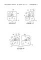
- Leftmost transistor 26can comprise any of the partially-masked configurations described with respect to FIG. 3.
- Rightmost transistor 26 ahas both source and drain regions masked, and constitutes other n-type transistor devices which do not receive a halo implant. As a result, the rightmost transistor 26 a has a lower threshold voltage V t than transistors receiving the halo implant.
- Leftmost transistor 26can comprise any of the partially-masked configurations described with respect to FIG. 3.
- Transistor 26 bhas both of its source and drain regions left exposed during the halo implant. Accordingly, halo regions 41 are formed proximate the source/drain regions of transistor 26 b.
- Leftmost transistor 26can comprise any of the partially-masked configurations described with respect to FIG. 3.
- portions of transistors in either the peripheral or the memory array regionare partially masked, and, in addition, the source regions and drain regions for some other individual transistor devices are masked, e.g. transistor 26 a, while different other individual peripheral transistor devices, e.g. transistor 26 b, have their source regions and drain regions exposed during the halo implant. Accordingly, where both of the source and drain regions are exposed, a pair of halo regions 41 is formed.
- These associated transistor devices having both source and drain regions exposedare, for purposes of this document, referred to as first transistor devices.
- a common masking stepis utilized and in a common implant step, a halo implant is conducted of devices formed over a substrate comprising memory circuitry and peripheral circuitry, sufficient to impart to at least three of the devices three different respective threshold voltages.
- the three devicescomprise NMOS field effect transistors.
- NMOS field effect transistorsin which the implanted halo impurity comprises a p-type impurity, those transistors whose source and drain regions are fully exposed, will typically have the highest threshold voltage V t1 .
- Those transistors which are partially masked during the halo implantwill typically have a threshold voltage V t2 which is somewhat lower than threshold voltage V t1 .
- Those transistors whose source and drain regions are completely blocked during the halo implantwill typically have the lowest threshold voltage V t3 of the threshold voltages. Accordingly, three different threshold voltages are provided through one common masking step.
- FIG. 7is a side sectional view of a semiconductor wafer fragment in process in accordance with one embodiment of the invention.
- Transistors 20 and 22 of FIG. 1now form memory access transistors 45 having a threshold voltage that corresponds to a single halo implant 41 on a bitline contact side of the access transistors 45 .
- Storage node sides 47 of the access transistors 45are masked by the masking layer 40 to prevent boron from being implanted. Forming access transistors 45 in this way improves refresh capabilities.
- the one-sided halo implant 41 in the access transistors 45allows the channel doping to be reduced while maintaining the same threshold voltage V t and subthreshold voltage. The lower channel doping, in turn, gives rise to improved DRAM refresh characteristics, because charge leakage from the storage nodes 47 is reduced.
- the halo implant and the mask 40 thereformay be effectuated before formation of sidewall spacers (denoted “SS” in FIG. 1), as shown in FIGS. 2 - 7 , or after formation of sidewall spacers (as shown in FIG. 1).
- the sidewall spacers SS shown in FIG. 1may be formed using conventional deposition, oxidation and/or etching techniques. It will be appreciated that when boron is implanted into a n-type device, n-well bias plugs and other conventional features should be masked to avoid compromise of the conductivity of these features.
- n-minus implant 37When the halo implant is done with a mask, prior to formation of sidewall spacers SS, it is normally accompanied by an n-minus implant 37 , using either phosphorous or arsenic. When the halo implant is done after formation of the sidewall spacers SS, it is assumed that the n-minus layer 37 was formed earlier as part of a LDD (lightly doped drain) structure. This same halo implant is normally accompanied by an n+ source drain implantation.
- LDDlightly doped drain
- One preferred application for such devicescan be in the context of peripheral circuitry comprising a so-called equilibrating device, which is typically connected between bit lines D and D* in dynamic random access memory circuitry in order to bring the bit lines to a common voltage potential (typically V cc /2) prior to firing the word lines to perform a sensing operation.
- a common voltage potentialtypically V cc /2
- Another applicationcan be for the cross-coupled transistors in a sense amplifier circuit, where lower threshold voltage V t is preferred for better margin and refresh properties.
- Other applicationscan include various low-voltage applications which will be apparent to the skilled artisan.
Landscapes
- Engineering & Computer Science (AREA)
- Manufacturing & Machinery (AREA)
- Metal-Oxide And Bipolar Metal-Oxide Semiconductor Integrated Circuits (AREA)
- Semiconductor Memories (AREA)
- Non-Volatile Memory (AREA)
Abstract
Description
- This invention relates generally to semiconductor processing methods of forming integrated circuitry, and particularly to methods of forming integrated circuit devices having different threshold voltages.[0001]
- Field effect transistors are characterized by a source region, a drain region and a gate. The source and drain regions are typically received within a semiconductive material, such as a semiconductive substrate. The gate is typically disposed elevationally over the source and drain regions. A gate voltage of sufficient minimum magnitude can be placed on the gate to induce a channel region underneath the gate and between the source and drain regions. Such channel-inducing voltage is typically referred to as the transistor's threshold voltage, or V[0002]t. Accordingly, the threshold voltage turns the transistor on. Once the magnitude of the threshold voltage has been exceeded, current can flow between the source and drain regions in accordance with a voltage called the source/drain voltage, or Vds.
- Threshold voltage magnitudes can be affected by channel implants. Specifically, during fabrication of semiconductor devices, a substrate can be implanted with certain types of impurity to modify or change the threshold voltage of a resultant device. Such channel implants can also affect a condition known as subsurface punchthrough. Punchthrough is a phenomenon which is associated with a merging of the source and drain depletion regions within a MOSFET. Specifically, as the channel gets shorter (as device dimensions get smaller), depletion region edges get closer together. When the channel length is decreased to roughly the sum of the two junction depletion widths, punchthrough is established. Punchthrough is an undesired effect in MOSFETS.[0003]
- One way of addressing punchthrough in sub-micron devices is through provision of a so-called halo implant, also known as a “pocket” implant. Halo implants are formed by implanting dopants (opposite in type to that of the source and drain) within the substrate proximate the source and drain regions, and are typically disposed underneath the channel region. The implanted halo dopant raises the doping concentration only on the inside walls of the source/drain junctions, so that the channel length can be decreased without needing to use a higher doped substrate. That is, punchthrough does not set in until a shorter channel length because of the halo.[0004]
- It is desirable to have MOSFETS with different threshold voltages depending upon the context in which the integrated circuitry of which they comprise a part is to be used. In the context of memory devices it can be beneficial to have transistors with different threshold voltages.[0005]
- This invention arose out of concerns associated with improving the methods through which integrated circuits are fabricated. In particular, the invention arose concerns associated with providing improved methods of forming memory devices.[0006]
- Semiconductor processing methods of forming integrated circuitry are described. In one embodiment, memory circuitry and peripheral circuitry are formed over a substrate. The peripheral circuitry comprises first and second type MOS transistors. Second type halo implants are conducted into the first type MOS transistors in less than all of the peripheral MOS transistors of the first type. In another embodiment, a plurality of n-type transistor devices are formed over a substrate and comprise memory array circuitry and peripheral circuitry. At least some of the individual peripheral circuitry n-type transistor devices are partially masked, and a halo implant is conducted for unmasked portions of the partially masked peripheral circuitry n-type transistor devices. In yet another embodiment, at least a portion of only one of the source and drain regions is masked, and at least a portion of the other of the source and drains regions is exposed for at least some of the peripheral circuitry n-type transistor devices. A halo implant is conducted relative to the exposed portions of the source and drain regions. In another embodiment, a common masking step is used and a halo implant is conducted of devices formed over a substrate comprising memory circuitry and peripheral circuitry sufficient to impart to at least three of the devices three different respective threshold voltages.[0007]
- Preferred embodiments of the invention are described below with reference to the following accompanying drawings.[0008]
- FIG. 1 is a diagrammatic side sectional view of a semiconductor wafer fragment in process, which is suitable for use in connection with one or more embodiments of the present invention.[0009]
- FIG. 2 is a side sectional view of a semiconductor wafer fragment in process in accordance with one embodiment of the invention.[0010]
- FIG. 3 is a side sectional view of a semiconductor wafer fragment in process in accordance with one embodiment of the invention.[0011]
- FIG. 4 is a side sectional view of a semiconductor wafer fragment in process in accordance with one embodiment of the invention.[0012]
- FIG. 5 is a side sectional view of a semiconductor wafer fragment in process in accordance with one embodiment of the invention.[0013]
- FIG. 6 is a side sectional view of a semiconductor wafer fragment in process in accordance with one embodiment of the invention.[0014]
- FIG. 7 is a side sectional view of a semiconductor wafer fragment in process in accordance with one embodiment of the invention.[0015]
- This disclosure of the invention is submitted in furtherance of the constitutional purposes of the U.S. Patent Laws “to promote the progress of science and useful arts” ([0016]
Article 1, Section 8). - Referring to FIG. 1, a semiconductor wafer fragment in process is shown generally at[0017]10 and includes a
semiconductive substrate 12. In the context of this document, the term “semiconductive substrate” is defined to mean any construction comprising semiconductive material, including, but not limited to, bulk semiconductive materials such as a semiconductive wafer (either alone or in assemblies comprising other materials thereon), and semiconductive material layers (either alone or in assemblies comprising other materials). The term “substrate” refers to any supporting structure, including, but not limited to, the semiconductive substrates described above. - [0018]
Memory array circuitry 14 andperipheral circuitry 16 are formed oversubstrate 12.Memory circuitry 14 comprisesindividual transistors Peripheral circuitry 16 comprises atransistor 26. These transistors are shown for example only. Each exemplary transistor will typically include a conductive gate line28 (designated fortransistors gate oxide layer 30, apolysilicon layer 32, asilicide layer 34, and an overlyinginsulative cap 36. Conventional sidewall spacers SS are optionally provided over the sidewalls ofgate line 28. Of course, other gate line constructions could be used. Source/drain regions substrate 12. - The[0019]
drain regions 37 may be formed in several different ways. In one embodiment, thedrain regions 37 are doped first with a blanket n-minus implant, which may be performed before or after formation of the sidewalls SS. As used herein, the term “blanket implant” refers to an implant process that does not employ a masking step. In one embodiment, thedrain regions 37 are doped by out-diffusion of dopants from a doped polysilicon layer forming a portion of astorage node 39. - The[0020]
source regions 38 may also be formed in several different ways. In one embodiment, the source regions are doped first with a blanket n-minus implant 37′ and then with a n-plus implant, followed by ahalo implant 41. - Typically, the transistors forming[0021]
peripheral circuitry 16 will include first- and second-type MOS transistors. For example and for purposes of the on-going discussion, first-type MOS transistors will comprise n-type transistors, and second-type MOS transistors will comprise p-type transistors. Similarly, in this example, implants comprising a second-type of material will comprise p-type implants such as boron. - Referring to FIGS. 2 and 3, a[0022]
masking layer 40 is formed oversubstrate 12. Transistor42 (FIG. 2) can constitute a transistor which is disposed within the memory array, or one which is disposed within the peripheral area. Similarly, transistor26 (FIG. 3) can constitute a transistor which is disposed within the memory array, or one which is disposed within the peripheral area.Transistor 26 can represent one of many similar partially-masked transistors in either the peripheral area or the memory array. In one embodiment, and with maskinglayer 40 in place, a second-type halo implant is conducted intotransistor 26 and in less than all transistors of the first type. The halo implant forms ahalo region 41 received withinsubstrate 12. In this case,transistor 42 can constitute a transistor which does not receive the halo implant. In one embodiment, when transistors receive the halo implant, only one side of the transistor receives the implant, such as shown in FIG. 3. This constitutes a different transistor having a different threshold voltage Vtthan those transistors not receiving the halo implant. - Specifically, in one embodiment,[0023]
transistor 26 comprises an n-type transistor device which is partially masked, and the halo implant is conducted for unmasked portions of the transistor or transistors. Various portions oftransistor 26 can be masked to result in a partially masked transistor. For example, at least a portion of one of the source and drain regions can be masked, and at least a portion of the other of the source and drain regions can be exposed. As a further example, a majority portion of one of the drain regions can be masked, while a majority portion of the other of the source regions is not masked for at least some of the devices. In the illustrated example, an entirety of one of the drain regions is masked, and the entirety of the other of the source regions is not masked. Where a transistor's source region is masked, after the halo implantation, the transistor will have a configuration similar to a source follower configuration. Where a transistor's drain region is masked, after the halo implantation, the transistor can have its electric field suppressed proximate the drain. - In another embodiment, the second-type halo implants are conducted into only one of the source and drain regions in less than all of the MOS transistors of the first type, and not the other of the source and drain regions of those peripheral MOS transistors of the first type.[0024]
- Referring to FIG. 4, another embodiment of the invention is shown.[0025]
Leftmost transistor 26 can comprise any of the partially-masked configurations described with respect to FIG. 3.Rightmost transistor 26ahas both source and drain regions masked, and constitutes other n-type transistor devices which do not receive a halo implant. As a result, therightmost transistor 26ahas a lower threshold voltage Vtthan transistors receiving the halo implant. - Referring to FIG. 5, another embodiment of the invention is shown.[0026]
Leftmost transistor 26 can comprise any of the partially-masked configurations described with respect to FIG. 3.Transistor 26bhas both of its source and drain regions left exposed during the halo implant. Accordingly,halo regions 41 are formed proximate the source/drain regions oftransistor 26b. - Referring to FIG. 6, another embodiment of the invention is shown.[0027]
Leftmost transistor 26 can comprise any of the partially-masked configurations described with respect to FIG. 3. In this embodiment, portions of transistors in either the peripheral or the memory array region are partially masked, and, in addition, the source regions and drain regions for some other individual transistor devices are masked,e.g. transistor 26a,while different other individual peripheral transistor devices,e.g. transistor 26b,have their source regions and drain regions exposed during the halo implant. Accordingly, where both of the source and drain regions are exposed, a pair ofhalo regions 41 is formed. These associated transistor devices having both source and drain regions exposed are, for purposes of this document, referred to as first transistor devices. Where both of the source and drain regions are masked or otherwise blocked, no halo regions are formed. These associated transistor devices having both source and drain regions masked or blocked are, for purposes of this document, referred to as second transistor devices. Where a portion of a transistor device is exposed, a halo region can, in some instances, be formed with respect to only one of the source and drain regions. These associated transistor devices are, for purposes of this document, referred to as third transistor devices. Preferably, these associated transistor devices are all NMOS transistor devices. - Alternately considered, and in a preferred embodiment, a common masking step is utilized and in a common implant step, a halo implant is conducted of devices formed over a substrate comprising memory circuitry and peripheral circuitry, sufficient to impart to at least three of the devices three different respective threshold voltages. In one embodiment, the three devices comprise NMOS field effect transistors.[0028]
- In the context of NMOS field effect transistors in which the implanted halo impurity comprises a p-type impurity, those transistors whose source and drain regions are fully exposed, will typically have the highest threshold voltage V[0029]t1. Those transistors which are partially masked during the halo implant will typically have a threshold voltage Vt2which is somewhat lower than threshold voltage Vt1. Those transistors whose source and drain regions are completely blocked during the halo implant will typically have the lowest threshold voltage Vt3of the threshold voltages. Accordingly, three different threshold voltages are provided through one common masking step.
- FIG. 7 is a side sectional view of a semiconductor wafer fragment in process in accordance with one embodiment of the invention.[0030]
Transistors memory access transistors 45 having a threshold voltage that corresponds to asingle halo implant 41 on a bitline contact side of theaccess transistors 45. Storage node sides47 of theaccess transistors 45 are masked by themasking layer 40 to prevent boron from being implanted. Formingaccess transistors 45 in this way improves refresh capabilities. The one-sided halo implant 41 in theaccess transistors 45 allows the channel doping to be reduced while maintaining the same threshold voltage Vtand subthreshold voltage. The lower channel doping, in turn, gives rise to improved DRAM refresh characteristics, because charge leakage from thestorage nodes 47 is reduced. - It will be appreciated that the halo implant and the[0031]
mask 40 therefor may be effectuated before formation of sidewall spacers (denoted “SS” in FIG. 1), as shown in FIGS.2-7, or after formation of sidewall spacers (as shown in FIG. 1). The sidewall spacers SS shown in FIG. 1 may be formed using conventional deposition, oxidation and/or etching techniques. It will be appreciated that when boron is implanted into a n-type device, n-well bias plugs and other conventional features should be masked to avoid compromise of the conductivity of these features. - When the halo implant is done with a mask, prior to formation of sidewall spacers SS, it is normally accompanied by an n-[0032]
minus implant 37, using either phosphorous or arsenic. When the halo implant is done after formation of the sidewall spacers SS, it is assumed that the n-minus layer 37 was formed earlier as part of a LDD (lightly doped drain) structure. This same halo implant is normally accompanied by an n+ source drain implantation. - One preferred application for such devices can be in the context of peripheral circuitry comprising a so-called equilibrating device, which is typically connected between bit lines D and D* in dynamic random access memory circuitry in order to bring the bit lines to a common voltage potential (typically V[0033]cc/2) prior to firing the word lines to perform a sensing operation. Another application can be for the cross-coupled transistors in a sense amplifier circuit, where lower threshold voltage Vtis preferred for better margin and refresh properties. Other applications can include various low-voltage applications which will be apparent to the skilled artisan.
- In compliance with the statute, the invention has been described in language more or less specific as to structural and methodical features. It is to be understood, however, that the invention is not limited to the specific features shown and described, since the means herein disclosed comprise preferred forms of putting the invention into effect. The invention is, therefore, claimed in any of its forms or modifications within the proper scope of the appended claims appropriately interpreted in accordance with the doctrine of equivalents.[0034]
Claims (49)
Priority Applications (8)
| Application Number | Priority Date | Filing Date | Title |
|---|---|---|---|
| US09/388,856US6579751B2 (en) | 1999-09-01 | 1999-09-01 | Semiconductor processing methods of forming integrated circuitry |
| US09/848,846US7341901B2 (en) | 1999-09-01 | 2001-05-03 | Semiconductor processing methods of forming integrated circuitry |
| US10/264,615US6875646B2 (en) | 1999-09-01 | 2002-10-03 | Semiconductor processing methods of forming integrated circuitry |
| US10/376,106US7176093B2 (en) | 1999-09-01 | 2003-02-26 | Semiconductor processing methods of forming integrated circuitry |
| US10/618,471US7045405B2 (en) | 1999-09-01 | 2003-07-11 | Semiconductor processing methods of forming integrated circuitry |
| US10/844,714US7135363B2 (en) | 1999-09-01 | 2004-05-12 | Semiconductor processing methods of forming integrated circuitry |
| US10/899,833US20050042810A1 (en) | 1999-09-01 | 2004-07-26 | Semiconductor processing methods of forming integrated circuitry |
| US11/437,970US20060211207A1 (en) | 1999-09-01 | 2006-05-19 | Semiconductor processing methods of forming integrated circuitry |
Applications Claiming Priority (1)
| Application Number | Priority Date | Filing Date | Title |
|---|---|---|---|
| US09/388,856US6579751B2 (en) | 1999-09-01 | 1999-09-01 | Semiconductor processing methods of forming integrated circuitry |
Related Child Applications (2)
| Application Number | Title | Priority Date | Filing Date |
|---|---|---|---|
| US09/848,846DivisionUS7341901B2 (en) | 1999-09-01 | 2001-05-03 | Semiconductor processing methods of forming integrated circuitry |
| US10/376,106ContinuationUS7176093B2 (en) | 1999-09-01 | 2003-02-26 | Semiconductor processing methods of forming integrated circuitry |
Publications (2)
| Publication Number | Publication Date |
|---|---|
| US20010051407A1true US20010051407A1 (en) | 2001-12-13 |
| US6579751B2 US6579751B2 (en) | 2003-06-17 |
Family
ID=23535820
Family Applications (8)
| Application Number | Title | Priority Date | Filing Date |
|---|---|---|---|
| US09/388,856Expired - LifetimeUS6579751B2 (en) | 1999-09-01 | 1999-09-01 | Semiconductor processing methods of forming integrated circuitry |
| US09/848,846Expired - Fee RelatedUS7341901B2 (en) | 1999-09-01 | 2001-05-03 | Semiconductor processing methods of forming integrated circuitry |
| US10/264,615Expired - LifetimeUS6875646B2 (en) | 1999-09-01 | 2002-10-03 | Semiconductor processing methods of forming integrated circuitry |
| US10/376,106Expired - LifetimeUS7176093B2 (en) | 1999-09-01 | 2003-02-26 | Semiconductor processing methods of forming integrated circuitry |
| US10/618,471Expired - Fee RelatedUS7045405B2 (en) | 1999-09-01 | 2003-07-11 | Semiconductor processing methods of forming integrated circuitry |
| US10/844,714Expired - LifetimeUS7135363B2 (en) | 1999-09-01 | 2004-05-12 | Semiconductor processing methods of forming integrated circuitry |
| US10/899,833AbandonedUS20050042810A1 (en) | 1999-09-01 | 2004-07-26 | Semiconductor processing methods of forming integrated circuitry |
| US11/437,970AbandonedUS20060211207A1 (en) | 1999-09-01 | 2006-05-19 | Semiconductor processing methods of forming integrated circuitry |
Family Applications After (7)
| Application Number | Title | Priority Date | Filing Date |
|---|---|---|---|
| US09/848,846Expired - Fee RelatedUS7341901B2 (en) | 1999-09-01 | 2001-05-03 | Semiconductor processing methods of forming integrated circuitry |
| US10/264,615Expired - LifetimeUS6875646B2 (en) | 1999-09-01 | 2002-10-03 | Semiconductor processing methods of forming integrated circuitry |
| US10/376,106Expired - LifetimeUS7176093B2 (en) | 1999-09-01 | 2003-02-26 | Semiconductor processing methods of forming integrated circuitry |
| US10/618,471Expired - Fee RelatedUS7045405B2 (en) | 1999-09-01 | 2003-07-11 | Semiconductor processing methods of forming integrated circuitry |
| US10/844,714Expired - LifetimeUS7135363B2 (en) | 1999-09-01 | 2004-05-12 | Semiconductor processing methods of forming integrated circuitry |
| US10/899,833AbandonedUS20050042810A1 (en) | 1999-09-01 | 2004-07-26 | Semiconductor processing methods of forming integrated circuitry |
| US11/437,970AbandonedUS20060211207A1 (en) | 1999-09-01 | 2006-05-19 | Semiconductor processing methods of forming integrated circuitry |
Country Status (1)
| Country | Link |
|---|---|
| US (8) | US6579751B2 (en) |
Cited By (6)
| Publication number | Priority date | Publication date | Assignee | Title |
|---|---|---|---|---|
| US6458665B1 (en)* | 1999-05-10 | 2002-10-01 | Hyundai Electronics Industries Co., Ltd. | Halo ion implantation method for fabricating a semiconductor device |
| US6630724B1 (en) | 2000-08-31 | 2003-10-07 | Micron Technology, Inc. | Gate dielectric antifuse circuits and methods for operating same |
| US20040041167A1 (en)* | 2002-08-29 | 2004-03-04 | Micron Technology, Inc. | Gate dielectric antifuse circuit to protect a high-voltage transistor |
| US20040042317A1 (en)* | 2002-08-29 | 2004-03-04 | Micron Technology, Inc. | Circuits and methods to protect a gate dielectric antifuse |
| WO2004025693A3 (en)* | 2002-09-02 | 2004-04-29 | Infineon Technologies Ag | Method for the production of a semi-conductive structure comprising a plurality of gate stacks arranged on a semi-conductor substrate and corresponding semi-conductive structure |
| US20040106253A1 (en)* | 1999-09-01 | 2004-06-03 | Tran Luan C. | Semiconductor processing methods of forming integrated circuitry |
Families Citing this family (13)
| Publication number | Priority date | Publication date | Assignee | Title |
|---|---|---|---|---|
| US6545904B2 (en)* | 2001-03-16 | 2003-04-08 | Micron Technology, Inc. | 6f2 dram array, a dram array formed on a semiconductive substrate, a method of forming memory cells in a 6f2 dram array and a method of isolating a single row of memory cells in a 6f2 dram array |
| WO2004004010A1 (en)* | 2002-06-28 | 2004-01-08 | Stmicroelectronics Nv | Method for the production of mos transistors |
| US7417285B2 (en)* | 2002-07-15 | 2008-08-26 | Kabushiki Kaisha Toshiba | Semiconductor device having a trench capacitor and a MOSFET connected by a diffusion layer and manufacturing method thereof |
| KR100580796B1 (en)* | 2003-12-10 | 2006-05-17 | 동부일렉트로닉스 주식회사 | Manufacturing Method of Semiconductor Device |
| KR100574172B1 (en)* | 2003-12-23 | 2006-04-27 | 동부일렉트로닉스 주식회사 | Manufacturing method of semiconductor device |
| KR100521440B1 (en)* | 2003-12-27 | 2005-10-13 | 동부아남반도체 주식회사 | Method for fabricating the halo region in NMOS transistor |
| JP2007258568A (en)* | 2006-03-24 | 2007-10-04 | Fujitsu Ltd | Manufacturing method of semiconductor device |
| US8822293B2 (en)* | 2008-03-13 | 2014-09-02 | Taiwan Semiconductor Manufacturing Company, Ltd. | Self-aligned halo/pocket implantation for reducing leakage and source/drain resistance in MOS devices |
| US7824973B2 (en)* | 2008-10-02 | 2010-11-02 | Infineon Technologies Ag | Method of forming a semiconductor device and semiconductor device thereof |
| US20100244151A1 (en)* | 2009-03-27 | 2010-09-30 | National Semiconductor Corporation | Structure and fabrication of field-effect transistor having source/drain extension defined by multiple local concentration maxima |
| US8026142B2 (en)* | 2009-05-08 | 2011-09-27 | Globalfoundries Inc. | Method of fabricating semiconductor transistor devices with asymmetric extension and/or halo implants |
| US8193062B2 (en)* | 2009-09-25 | 2012-06-05 | International Business Machines Corporation | Asymmetric silicon-on-insulator SRAM cell |
| US10026837B2 (en)* | 2015-09-03 | 2018-07-17 | Texas Instruments Incorporated | Embedded SiGe process for multi-threshold PMOS transistors |
Family Cites Families (40)
| Publication number | Priority date | Publication date | Assignee | Title |
|---|---|---|---|---|
| US203745A (en)* | 1878-05-14 | Improvement in stench-valves for wash-basins | ||
| US4417325A (en) | 1981-07-13 | 1983-11-22 | Eliyahou Harari | Highly scaleable dynamic ram cell with self-signal amplification |
| JPS62174968A (en) | 1986-01-29 | 1987-07-31 | Hitachi Ltd | semiconductor equipment |
| US5272367A (en)* | 1988-05-02 | 1993-12-21 | Micron Technology, Inc. | Fabrication of complementary n-channel and p-channel circuits (ICs) useful in the manufacture of dynamic random access memories (drams) |
| US5252504A (en)* | 1988-05-02 | 1993-10-12 | Micron Technology, Inc. | Reverse polysilicon CMOS fabrication |
| KR100199258B1 (en)* | 1990-02-09 | 1999-06-15 | 가나이 쓰도무 | Semiconductor integrated circuit device |
| US5371026A (en)* | 1992-11-30 | 1994-12-06 | Motorola Inc. | Method for fabricating paired MOS transistors having a current-gain differential |
| FI94909C (en)* | 1994-04-19 | 1995-11-10 | Valtion Teknillinen | Acoustic flow measurement method and applicable device |
| US5773863A (en)* | 1994-08-18 | 1998-06-30 | Sun Microsystems, Inc. | Low power, high performance junction transistor |
| KR960026960A (en)* | 1994-12-16 | 1996-07-22 | 리 패치 | Asymmetric Low Power Morse Device |
| US5661054A (en)* | 1995-05-19 | 1997-08-26 | Micron Technology, Inc. | Method of forming a non-volatile memory array |
| US6004854A (en) | 1995-07-17 | 1999-12-21 | Micron Technology, Inc. | Method of forming CMOS integrated circuitry |
| US5534449A (en)* | 1995-07-17 | 1996-07-09 | Micron Technology, Inc. | Methods of forming complementary metal oxide semiconductor (CMOS) integrated circuitry |
| US5786249A (en)* | 1996-03-07 | 1998-07-28 | Micron Technology, Inc. | Method of forming dram circuitry on a semiconductor substrate |
| US5706806A (en)* | 1996-04-26 | 1998-01-13 | Bioanalytical Systems, Inc. | Linear microdialysis probe with support fiber |
| US6166840A (en)* | 1996-04-29 | 2000-12-26 | Esel-Krabbe Systems A/S | Electronic circuit for receiving and discriminating modulated light and an electronic price display comprising said circuit |
| US6020244A (en) | 1996-12-30 | 2000-02-01 | Intel Corporation | Channel dopant implantation with automatic compensation for variations in critical dimension |
| JP3272979B2 (en)* | 1997-01-08 | 2002-04-08 | 株式会社東芝 | Semiconductor device |
| US5837584A (en)* | 1997-01-15 | 1998-11-17 | Macronix International Co., Ltd. | Virtual ground flash cell with asymmetrically placed source and drain and method of fabrication |
| US5963808A (en)* | 1997-01-15 | 1999-10-05 | Macronix International Co., Ltd. | Method of forming an asymmetric bird's beak cell for a flash EEPROM |
| KR100399291B1 (en)* | 1997-01-27 | 2004-01-24 | 가부시키가이샤 아드반스트 디스프레이 | Liquid crystal display device using semiconductor thin film transistor, manufacturing method thereof, semiconductor thin film transistor array substrate and corresponding semiconductor thin film transistor array substrate |
| TW417256B (en)* | 1997-01-31 | 2001-01-01 | Seiko Epson Corp | Semiconductor MOS device and its manufacturing method |
| US6008080A (en)* | 1997-11-21 | 1999-12-28 | United Microelectronics Corp. | Method of making a low power SRAM |
| US6312997B1 (en)* | 1998-08-12 | 2001-11-06 | Micron Technology, Inc. | Low voltage high performance semiconductor devices and methods |
| GB2343240A (en)* | 1998-10-26 | 2000-05-03 | Michael Ernest Saxby | Projectiles |
| US6200863B1 (en)* | 1999-03-24 | 2001-03-13 | Advanced Micro Devices, Inc. | Process for fabricating a semiconductor device having assymetric source-drain extension regions |
| US6238967B1 (en)* | 1999-04-12 | 2001-05-29 | Motorola, Inc. | Method of forming embedded DRAM structure |
| US6391756B1 (en)* | 1999-08-31 | 2002-05-21 | Micron Technology, Inc. | Semiconductor processing methods of forming contact openings |
| US6579751B2 (en)* | 1999-09-01 | 2003-06-17 | Micron Technology, Inc. | Semiconductor processing methods of forming integrated circuitry |
| TW451317B (en)* | 2000-03-24 | 2001-08-21 | Vanguard Int Semiconduct Corp | Manufacturing method of asymmetrical source/drain of DRAM cell |
| JP3938462B2 (en)* | 2000-06-27 | 2007-06-27 | 株式会社リコー | Mounting structure for solid-state imaging device, imaging unit, and image reading apparatus having the imaging unit |
| US6455362B1 (en)* | 2000-08-22 | 2002-09-24 | Micron Technology, Inc. | Double LDD devices for improved dram refresh |
| US6545904B2 (en)* | 2001-03-16 | 2003-04-08 | Micron Technology, Inc. | 6f2 dram array, a dram array formed on a semiconductive substrate, a method of forming memory cells in a 6f2 dram array and a method of isolating a single row of memory cells in a 6f2 dram array |
| US6466489B1 (en)* | 2001-05-18 | 2002-10-15 | International Business Machines Corporation | Use of source/drain asymmetry MOSFET devices in dynamic and analog circuits |
| KR100434702B1 (en)* | 2001-12-27 | 2004-06-07 | 주식회사 하이닉스반도체 | Method of manufacturing semiconductor device to improve refresh property |
| KR100470388B1 (en)* | 2002-05-03 | 2005-02-07 | 주식회사 하이닉스반도체 | Dram cell having independent and asymmetric source/drain and method for forming the same |
| US6620679B1 (en)* | 2002-08-20 | 2003-09-16 | Taiwan Semiconductor Manufacturing Company | Method to integrate high performance 1T ram in a CMOS process using asymmetric structure |
| JP4232675B2 (en)* | 2004-04-01 | 2009-03-04 | セイコーエプソン株式会社 | Manufacturing method of semiconductor device |
| US6972230B1 (en)* | 2004-06-10 | 2005-12-06 | Macronix International Co., Ltd. | Method for fabricating a floating gate memory device |
| KR100642407B1 (en)* | 2004-12-29 | 2006-11-08 | 주식회사 하이닉스반도체 | Method for manufacturing cell transistor of semiconductor memory device |
- 1999
- 1999-09-01USUS09/388,856patent/US6579751B2/ennot_activeExpired - Lifetime
- 2001
- 2001-05-03USUS09/848,846patent/US7341901B2/ennot_activeExpired - Fee Related
- 2002
- 2002-10-03USUS10/264,615patent/US6875646B2/ennot_activeExpired - Lifetime
- 2003
- 2003-02-26USUS10/376,106patent/US7176093B2/ennot_activeExpired - Lifetime
- 2003-07-11USUS10/618,471patent/US7045405B2/ennot_activeExpired - Fee Related
- 2004
- 2004-05-12USUS10/844,714patent/US7135363B2/ennot_activeExpired - Lifetime
- 2004-07-26USUS10/899,833patent/US20050042810A1/ennot_activeAbandoned
- 2006
- 2006-05-19USUS11/437,970patent/US20060211207A1/ennot_activeAbandoned
Cited By (18)
| Publication number | Priority date | Publication date | Assignee | Title |
|---|---|---|---|---|
| US6458665B1 (en)* | 1999-05-10 | 2002-10-01 | Hyundai Electronics Industries Co., Ltd. | Halo ion implantation method for fabricating a semiconductor device |
| US20040106253A1 (en)* | 1999-09-01 | 2004-06-03 | Tran Luan C. | Semiconductor processing methods of forming integrated circuitry |
| US7045405B2 (en)* | 1999-09-01 | 2006-05-16 | Micron Technology, Inc. | Semiconductor processing methods of forming integrated circuitry |
| US20060097345A1 (en)* | 2000-08-31 | 2006-05-11 | Micron Technology, Inc. | Gate dielectric antifuse circuits and methods for operating same |
| US20040065941A1 (en)* | 2000-08-31 | 2004-04-08 | Micron Technology, Inc. | Gate dielectric antifuse circuits and methods for operating same |
| US6630724B1 (en) | 2000-08-31 | 2003-10-07 | Micron Technology, Inc. | Gate dielectric antifuse circuits and methods for operating same |
| US7030458B2 (en) | 2000-08-31 | 2006-04-18 | Micron Technology, Inc. | Gate dielectric antifuse circuits and methods for operating same |
| US6751150B2 (en) | 2002-08-29 | 2004-06-15 | Micron Technology, Inc. | Circuits and method to protect a gate dielectric antifuse |
| US20040155315A1 (en)* | 2002-08-29 | 2004-08-12 | Micron Technology, Inc. | Circuits and methods to protect a gate dielectric antifuse |
| US20050029598A1 (en)* | 2002-08-29 | 2005-02-10 | Micron Technology, Inc. | Gate dielectric antifuse circuit to protect a high-voltage transistor |
| US6936909B2 (en) | 2002-08-29 | 2005-08-30 | Micron Technology, Inc. | Gate dielectric antifuse circuit to protect a high-voltage transistor |
| US20040042317A1 (en)* | 2002-08-29 | 2004-03-04 | Micron Technology, Inc. | Circuits and methods to protect a gate dielectric antifuse |
| US20040041167A1 (en)* | 2002-08-29 | 2004-03-04 | Micron Technology, Inc. | Gate dielectric antifuse circuit to protect a high-voltage transistor |
| US7101738B2 (en) | 2002-08-29 | 2006-09-05 | Micron Technology, Inc. | Gate dielectric antifuse circuit to protect a high-voltage transistor |
| US20060231922A1 (en)* | 2002-08-29 | 2006-10-19 | Micron Technology, Inc. | Gate dielectric antifuse circuit to protect a high-voltage transistor |
| US7126871B2 (en) | 2002-08-29 | 2006-10-24 | Micron Technology, Inc. | Circuits and methods to protect a gate dielectric antifuse |
| US7405463B2 (en) | 2002-08-29 | 2008-07-29 | Micron Technology, Inc. | Gate dielectric antifuse circuit to protect a high-voltage transistor |
| WO2004025693A3 (en)* | 2002-09-02 | 2004-04-29 | Infineon Technologies Ag | Method for the production of a semi-conductive structure comprising a plurality of gate stacks arranged on a semi-conductor substrate and corresponding semi-conductive structure |
Also Published As
| Publication number | Publication date |
|---|---|
| US6875646B2 (en) | 2005-04-05 |
| US20030153138A1 (en) | 2003-08-14 |
| US20030036235A1 (en) | 2003-02-20 |
| US20040209421A1 (en) | 2004-10-21 |
| US7176093B2 (en) | 2007-02-13 |
| US7045405B2 (en) | 2006-05-16 |
| US20060211207A1 (en) | 2006-09-21 |
| US7341901B2 (en) | 2008-03-11 |
| US7135363B2 (en) | 2006-11-14 |
| US20010018251A1 (en) | 2001-08-30 |
| US20040106253A1 (en) | 2004-06-03 |
| US6579751B2 (en) | 2003-06-17 |
| US20050042810A1 (en) | 2005-02-24 |
Similar Documents
| Publication | Publication Date | Title |
|---|---|---|
| US20060211207A1 (en) | Semiconductor processing methods of forming integrated circuitry | |
| US7195995B2 (en) | Method of manufacturing a multilayered doped conductor for a contact in an integrated circuit device | |
| US20010054734A1 (en) | Methods of forming integrated circuits using masks to provide ion implantation shielding to portions of a substrate adjacent to an isolation region therein and integrated circuits formed using same | |
| US7253047B2 (en) | Semiconductor processing methods of forming transistors, semiconductor processing methods of forming dynamic random access memory circuitry, and related integrated circuitry | |
| KR100214841B1 (en) | Semiconductor device and its fabrication process | |
| KR100486187B1 (en) | Semiconductor device and its manufacturing method | |
| KR100302648B1 (en) | Semiconductor device and manufacturing method thereof | |
| US10134744B1 (en) | Semiconductor memory device | |
| US20070018253A1 (en) | Memory cell and manufacturing methods | |
| US5986314A (en) | Depletion mode MOS capacitor with patterned Vt implants | |
| US7554130B1 (en) | Reducing effects of parasitic transistors in thyristor-based memory using an isolation or damage region | |
| US6413814B2 (en) | Manufacture of a semiconductor device with retrograded wells | |
| JPH1056147A (en) | Semiconductor device and manufacturing method thereof | |
| US4811066A (en) | Compact multi-state ROM cell | |
| KR0170311B1 (en) | Static random access memory and manufacturing method thereof | |
| JP3102923B2 (en) | Semiconductor storage device | |
| US7588991B2 (en) | Method for fabricating embedded static random access memory | |
| US6686635B2 (en) | Four transistors static-random-access-memory | |
| US8174046B1 (en) | Reducing effects of parasitic transistors in thyristor-based memory using local thinning or implanting | |
| US7259060B2 (en) | Method for fabricating a semiconductor structure | |
| US5548548A (en) | Pass transistor for a 256 megabit dram with negatively biased substrate | |
| JP3146993B2 (en) | Semiconductor device and manufacturing method thereof | |
| KR100195189B1 (en) | Fabrication method of semiconductor device | |
| JP2000323686A (en) | DRAM cell with reduced transfer device leakage and method of manufacturing the same |
Legal Events
| Date | Code | Title | Description |
|---|---|---|---|
| AS | Assignment | Owner name:MICRON TECHNOLOGY, INC., IDAHO Free format text:ASSIGNMENT OF ASSIGNORS INTEREST;ASSIGNOR:TRAN, LUAN C.;REEL/FRAME:010222/0552 Effective date:19990831 | |
| STCF | Information on status: patent grant | Free format text:PATENTED CASE | |
| FPAY | Fee payment | Year of fee payment:4 | |
| FPAY | Fee payment | Year of fee payment:8 | |
| FPAY | Fee payment | Year of fee payment:12 | |
| AS | Assignment | Owner name:U.S. BANK NATIONAL ASSOCIATION, AS COLLATERAL AGENT, CALIFORNIA Free format text:SECURITY INTEREST;ASSIGNOR:MICRON TECHNOLOGY, INC.;REEL/FRAME:038669/0001 Effective date:20160426 Owner name:U.S. BANK NATIONAL ASSOCIATION, AS COLLATERAL AGEN Free format text:SECURITY INTEREST;ASSIGNOR:MICRON TECHNOLOGY, INC.;REEL/FRAME:038669/0001 Effective date:20160426 | |
| AS | Assignment | Owner name:MORGAN STANLEY SENIOR FUNDING, INC., AS COLLATERAL AGENT, MARYLAND Free format text:PATENT SECURITY AGREEMENT;ASSIGNOR:MICRON TECHNOLOGY, INC.;REEL/FRAME:038954/0001 Effective date:20160426 Owner name:MORGAN STANLEY SENIOR FUNDING, INC., AS COLLATERAL Free format text:PATENT SECURITY AGREEMENT;ASSIGNOR:MICRON TECHNOLOGY, INC.;REEL/FRAME:038954/0001 Effective date:20160426 | |
| AS | Assignment | Owner name:U.S. BANK NATIONAL ASSOCIATION, AS COLLATERAL AGENT, CALIFORNIA Free format text:CORRECTIVE ASSIGNMENT TO CORRECT THE REPLACE ERRONEOUSLY FILED PATENT #7358718 WITH THE CORRECT PATENT #7358178 PREVIOUSLY RECORDED ON REEL 038669 FRAME 0001. ASSIGNOR(S) HEREBY CONFIRMS THE SECURITY INTEREST;ASSIGNOR:MICRON TECHNOLOGY, INC.;REEL/FRAME:043079/0001 Effective date:20160426 Owner name:U.S. BANK NATIONAL ASSOCIATION, AS COLLATERAL AGEN Free format text:CORRECTIVE ASSIGNMENT TO CORRECT THE REPLACE ERRONEOUSLY FILED PATENT #7358718 WITH THE CORRECT PATENT #7358178 PREVIOUSLY RECORDED ON REEL 038669 FRAME 0001. ASSIGNOR(S) HEREBY CONFIRMS THE SECURITY INTEREST;ASSIGNOR:MICRON TECHNOLOGY, INC.;REEL/FRAME:043079/0001 Effective date:20160426 | |
| AS | Assignment | Owner name:JPMORGAN CHASE BANK, N.A., AS COLLATERAL AGENT, ILLINOIS Free format text:SECURITY INTEREST;ASSIGNORS:MICRON TECHNOLOGY, INC.;MICRON SEMICONDUCTOR PRODUCTS, INC.;REEL/FRAME:047540/0001 Effective date:20180703 Owner name:JPMORGAN CHASE BANK, N.A., AS COLLATERAL AGENT, IL Free format text:SECURITY INTEREST;ASSIGNORS:MICRON TECHNOLOGY, INC.;MICRON SEMICONDUCTOR PRODUCTS, INC.;REEL/FRAME:047540/0001 Effective date:20180703 | |
| AS | Assignment | Owner name:MICRON TECHNOLOGY, INC., IDAHO Free format text:RELEASE BY SECURED PARTY;ASSIGNOR:U.S. BANK NATIONAL ASSOCIATION, AS COLLATERAL AGENT;REEL/FRAME:047243/0001 Effective date:20180629 | |
| AS | Assignment | Owner name:MICRON TECHNOLOGY, INC., IDAHO Free format text:RELEASE BY SECURED PARTY;ASSIGNOR:MORGAN STANLEY SENIOR FUNDING, INC., AS COLLATERAL AGENT;REEL/FRAME:050937/0001 Effective date:20190731 | |
| AS | Assignment | Owner name:MICRON TECHNOLOGY, INC., IDAHO Free format text:RELEASE BY SECURED PARTY;ASSIGNOR:JPMORGAN CHASE BANK, N.A., AS COLLATERAL AGENT;REEL/FRAME:051028/0001 Effective date:20190731 Owner name:MICRON SEMICONDUCTOR PRODUCTS, INC., IDAHO Free format text:RELEASE BY SECURED PARTY;ASSIGNOR:JPMORGAN CHASE BANK, N.A., AS COLLATERAL AGENT;REEL/FRAME:051028/0001 Effective date:20190731 |