US20010043274A1 - Optical test structure for measuring charge-transfer efficiency - Google Patents
Optical test structure for measuring charge-transfer efficiencyDownload PDFInfo
- Publication number
- US20010043274A1 US20010043274A1US09/736,936US73693600AUS2001043274A1US 20010043274 A1US20010043274 A1US 20010043274A1US 73693600 AUS73693600 AUS 73693600AUS 2001043274 A1US2001043274 A1US 2001043274A1
- Authority
- US
- United States
- Prior art keywords
- column
- photoactive
- image sensor
- shift register
- horizontal shift
- Prior art date
- Legal status (The legal status is an assumption and is not a legal conclusion. Google has not performed a legal analysis and makes no representation as to the accuracy of the status listed.)
- Granted
Links
- 238000012546transferMethods0.000titleclaimsabstractdescription58
- 238000012360testing methodMethods0.000titleclaimsabstractdescription25
- 230000003287optical effectEffects0.000titleabstractdescription50
- 239000000463materialSubstances0.000abstractdescription4
- 239000002184metalSubstances0.000abstractdescription3
- 238000001444catalytic combustion detectionMethods0.000abstract8
- 239000000758substrateSubstances0.000abstract3
- 239000004065semiconductorSubstances0.000abstract1
- 238000002347injectionMethods0.000description46
- 239000007924injectionSubstances0.000description46
- 230000002000scavenging effectEffects0.000description19
- 238000009792diffusion processMethods0.000description11
- 238000012512characterization methodMethods0.000description4
- 238000010586diagramMethods0.000description4
- 238000003491arrayMethods0.000description3
- 238000005259measurementMethods0.000description3
- 238000011065in-situ storageMethods0.000description2
- 238000012544monitoring processMethods0.000description2
- 230000005855radiationEffects0.000description2
- 238000010521absorption reactionMethods0.000description1
- 239000003086colorantSubstances0.000description1
- 238000003384imaging methodMethods0.000description1
- 238000004519manufacturing processMethods0.000description1
- 238000012986modificationMethods0.000description1
- 230000004048modificationEffects0.000description1
- 238000012552reviewMethods0.000description1
- 230000035945sensitivityEffects0.000description1
- 230000007704transitionEffects0.000description1
Images


Classifications
- H—ELECTRICITY
- H10—SEMICONDUCTOR DEVICES; ELECTRIC SOLID-STATE DEVICES NOT OTHERWISE PROVIDED FOR
- H10F—INORGANIC SEMICONDUCTOR DEVICES SENSITIVE TO INFRARED RADIATION, LIGHT, ELECTROMAGNETIC RADIATION OF SHORTER WAVELENGTH OR CORPUSCULAR RADIATION
- H10F39/00—Integrated devices, or assemblies of multiple devices, comprising at least one element covered by group H10F30/00, e.g. radiation detectors comprising photodiode arrays
- H10F39/10—Integrated devices
- H10F39/12—Image sensors
- H10F39/15—Charge-coupled device [CCD] image sensors
- H10F39/151—Geometry or disposition of pixel elements, address lines or gate electrodes
- H10F39/1515—Optical shielding
- H—ELECTRICITY
- H10—SEMICONDUCTOR DEVICES; ELECTRIC SOLID-STATE DEVICES NOT OTHERWISE PROVIDED FOR
- H10F—INORGANIC SEMICONDUCTOR DEVICES SENSITIVE TO INFRARED RADIATION, LIGHT, ELECTROMAGNETIC RADIATION OF SHORTER WAVELENGTH OR CORPUSCULAR RADIATION
- H10F39/00—Integrated devices, or assemblies of multiple devices, comprising at least one element covered by group H10F30/00, e.g. radiation detectors comprising photodiode arrays
- H10F39/10—Integrated devices
- H10F39/12—Image sensors
- H10F39/15—Charge-coupled device [CCD] image sensors
- H10F39/153—Two-dimensional or three-dimensional array CCD image sensors
- H10F39/1536—Frame transfer
Definitions
- the present inventionrelates to a charge-coupled device (CCD) solid-state image sensor having a built in test structure which utilizes an optical injection to measure the charge transfer efficiency for a CCD solid-state image sensor.
- CCDcharge-coupled device
- CCD image sensorsMany high-end imaging applications today utilize large format, area CCD image sensors. These area arrays are composed of a two-dimensional array of pixels, often called the vertical or parallel registers, that are usually transferred row by row into a single row, often called the horizontal or serial register that is used to clock out the signal. Some sensors may have more than one horizontal register.
- the benefits of this architectureare the high sensitivity, high charge capacity and low dark currents resulting in very large dynamic ranges.
- An important measure of performance for these large format imager sensorsis charge transfer efficiency (CTE), which measures how completely charge is transferred along a CCD register.
- CTEcharge transfer efficiency
- CTICTE in both the vertical and horizontal registers
- good CTE in the horizontal registeris more difficult to achieve because of the higher clock frequency, or, alternatively, the short time available to transfer charge from one phase to the next. Since many of the large format image sensors now require well over 5000 transfers in a register, CTI of less than 10 ⁇ 5 (or CTE>0.99999) is important to maintain signal integrity and prevent contrast loss and color errors.
- CTEis typically measured by the inclusion of a “fill and spill” electrical injection circuit (M. F. Tompsett, IEEE Transactions on Electron Devices, ED-22, No. 6, June 1975, pp. 305-309 and W. F. Kosonocky and J. E. Cames, RCA Review, 36, p. 566, September 1975, incorporated herein by reference) incorporated on the input end of the CCD shift register (usually the horizontal).
- the difficulty with electrical injection structuresis that they require adjustment for each individual die, thus making automation of testing more difficult.
- these small gatesare sensitive to electrostatic discharge (ESD); loss of an otherwise functional device can result from ESD failure of the test structure.
- X-ray radiation sourcessuch as Fe 55
- Fe 55provide a known and constant input level, but the additional apparatus and safety precautions inhibit its use in a production test environment.
- the fixed energy levels of a particular isotopealso prohibit the ability of measuring CTE as a function of signal level.
- one of the most useful sources, Fe 55has a limited useful lifetime.
- Optical injectioni.e., the use of optically generated packets
- Herbert J. ErhardtU.S. Pat. No. 5,369,357 of Nov. 29, 1994 incorporated herein by reference, describes an implementation for linear CCD arrays. This requires separate gate controls to transfer the optically generated packets into the CCD register for characterization of CTE. This would be difficult to implement for area arrays.
- This inventionincorporates special pixels in the CCD imager that enable in-situ monitoring of CTE.
- These special pixelsinclude a photoactive column (or columns) at the leading and trailing edge of the device beyond the dark reference regions. This column (or columns) is referred to as a vertical optical injection column.
- a charge packet for the CTE measurementis “injected” from the vertical optical injection column into the horizontal register by a normal row transfer.
- adjacent scavenging columnsIn order to remove optical and diffusion crosstalk components arriving from the photoactive column, adjacent scavenging columns are added that transfer charge in the opposite direction of normal vertical charge transfer. These scavenging columns collect charge generated by stray light or charge generated below the depletion region of the optically active pixels that diffuses to the adjacent scavenging columns. These scavenging columns are electrically connected to drains at the top of the array to remove any charge collected in these pixels. The scavenging columns are not electrically connected to the horizontal CCD register; thus no charge is transferred from a vertical row into the corresponding pixels of the horizontal register under the scavenging columns.
- the only charge read out from the horizontal pixel that follows the pixel containing the optical injection signalmust come from charge that was not transferred so that an accurate measurement of CTE can be made.
- the input stimulusis supplied by illuminating the sensor with light. Varying light intensity or exposure produces a transfer curve of transfer efficiency as a function of signal. For each different exposure, there will be a resultant signal level.
- the resulting horizontal profilecan be used to calculate the transfer efficiency in the case of few transfers (leading edge) and many transfers (trailing edge). If the sensor is uniformly illuminated or if it is read out such that the same charge is transferred from each pixel of the optical injection column or columns, horizontal profiles may be averaged to improve the accuracy of the CTE calculation. Software routines within a camera can use this information to compensate for such inefficiencies.
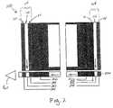
- FIG. 1is a schematic architectural diagram of an image sensor
- FIG. 2is a schematic diagram illustrating detail of the dark area along the edge of the image sensor shown in FIG. 1;
- FIG. 3is a graph illustrating a plot of the signal value of the light sensitive column as a function of signal found in the adjacent trailing column;
- FIG. 4is a schematic diagram illustrating an image sensor
- FIG. 5is a plot of signal vs. column number for the structure shown in FIG. 4;
- FIG. 6is a schematic diagram showing a detailed cross section for a portion of the image sensor shown in FIG. 4;
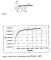
- FIG. 7is a transfer curve of horizontal CTE vs. signal level.
- the fullframe CCD image sensor shown in FIG. 1is used as an exemplary image sensor 100 in the following discussion. Not all aspects of the structure shown in FIG. 1 are known conventionally. Vertical CCD shift registers are formed, which serves as both the integrating photoactive region and for parallel (line by line) readout of the pixels.
- Each vertical (parallel) registerincludes a rectangular array of pixels.
- the photoactive area or image area, 103is usually surrounded by a dark reference area 102 comprising pixels covered with an opaque material or light shield 1021 , such as metal, which blocks the incident radiation of interest.
- a horizontal register, 200accepts each row or line from the vertical registers one at a time, and shifts charge packets from the pixels to a single output node V out in a serial fashion.
- the output node V outconverts each charge packet into a voltage, which can be processed and digitized.
- optical injection structure 104Contained within the column grouping forming the optical injection structure 104 (see FIG. 2) at the leading and trailing edges of the device beyond the dark reference regions 102 are special pixels that enable in-situ monitoring of CTE. As shown in FIG. 2, these pixels include optical injection columns 110 and 112 , which are photoactive and are bounded on each side by scavenging columns 114 . In order to remove optical and diffusion crosstalk components and spurious charges from the periphery 1102 (FIG. 4), scavenging columns 114 are added on both sides of the optical injection columns 110 and 112 .
- the scavenging columns 114may be covered with an opaque material such as metal and transfer any collected charge in the opposite direction of normal vertical charge transfer to a drain (as shown by the arrows in FIG. 2). More importantly, since the scavenging columns are not connected to the horizontal register 200 , no spurious signal is transferred into the horizontal pixels 214 of the horizontal register. As shown in FIG. 4, a drain 1104 at the top of the array is electrically connected to the scavenging columns 114 to remove any charge collected in these scavenging pixels.
- the input stimulusis supplied by illuminating the sensor with light. Electrons generated by this light in the optical injection columns 110 and 112 are “injected” or transferred from each row into pixels 210 and 212 , respectively of the horizontal register 200 .
- the resulting horizontal profileshown in FIG. 5, can be used to calculate the transfer efficiency in the case of few transfers (leading edge) and many transfers (trailing edge).
- Horizontal charge transfer efficiencyis composed of several components; among these are charge transfer from the first phase of the horizontal register over the gate onto the output structure and transfer along the horizontal register.
- the optical injection structure 104 at the leading edgewhich includes the optical injection column 110 , primarily measures the CTE over the first gate onto the output structure, since there are so few transfers from the optical injection column 110 to the output.
- the CTE along the horizontal registerusually dominates for the optical injection structure 104 at the trailing edge, containing the optical injection column 112 , since this typically involves thousands of transfers.
- FIG. 7shows a typical transfer curve for the case of injection from optical injection column 112 at the trailing edge of the register.
- the inventionprovides an optical structure for injecting charge into the horizontal register of an area-array CCD image sensor for characterization and calibration of the horizontal register.
- This structurecan be used to measure the charge-transfer efficiency (CTE) of the horizontal register versus signal level.
- CTEcharge-transfer efficiency
- FIG. 5shows a plot of the signal at the output amplifier vs. column number for a typical line of the imager.
- the signal 1300 from the “dummy” or overclock regioncontains no charge. This is the zero reference level for the image.
- the signal 1302 from the first optical injection column 110is followed by the trailing signal 1314 in the trailing horizontal pixel 214 .
- Scavenging columns 114do not contribute any signal to horizontal pixels 214 since the columns are not connected to the horizontal register 200 .
- the trailing signal 1314is only due to charge left behind due to transfer inefficiency. It is usually more useful to consider the size of 1314 for the leading optical injection structure 104 rather than the CTI, since there are so few transfers.
- the box 1303represents signal lost by CTI (which shows up as 1314 in the trailing pixel) and signal lost by diffusion from the optical injection columns 110 to the scavenging columns 114 .
- the signal 1306is the dark current signal from the dark reference columns under the light shield 1021 .
- the dark reference column adjacent to the first photoactive column in the image area 103has an additional signal 1310 which is partly composed of the signal 1316 lost due to diffusion of photo-generated electrons under the first photoactive column of the image area 103 . All other photoactive columns in the image area 103 lose charge due to diffusion, but most of them also gain diffusion charge from adjacent columns. The first and last photoactive columns have less signal because they don't have a photoactive column on one side to contribute diffusion charge.
- the first and last “few” columnsshould have less signal, depending on the wavelength of the incident light, but this application simplifies, to first order for the sake of ease of understanding.
- This size of the signals 1310 and 1311depends on the wavelength of light. The signal is smaller for incident blue light and grows larger as the incident wavelength grows larger (redder). Incident light with a longer wavelength (red) will create a larger diffusion signal 1310 (or 1311 ) since it has a longer absorption depth. Charge is generated further below the pixel depletion (or collection) region and more will by diffuse to adjacent pixels.
- Each row of the image area 103contributes signal 1308 , which is transferred to pixels 203 of the horizontal register.
- the sensoris illuminated with a spatially uniform light source.
- the signal in the last photoactive column of the image area 103also experiences a signal loss 1316 due to diffusion of charge to the dark reference region 102 .
- This lost signalshows up as a part of the additional signal 1311 in the first trailing column of the dark reference region 102 .
- Optical crosstalkalso contributes to 1311 .
- the signal 1311also has a component due to CTI, since this pixel trails a photoactive column.
- FIG. 6illustrates an exploded detail cross section of the circle shown as item 1100 in FIG. 4. More specifically, FIG. 6 illustrates the dark reference region 102 and a few of the pixels 1200 that are adjacent to an edge of the dark reference region 102 .
- Light 1204 that is incident at the edge of the dark reference light shield 1021may be “piped” by the optical waveguiding of the layers to pixels 1200 .
- electrons 1202 generated below the depletion regionalso may diffuse to pixels 1200 .
- This extra signal in pixels 1200is due to optical and diffusive crosstalk and to CTI.
- This signal 1311 from the first trailing dark reference column of the dark reference region 102is transferred into the horizontal register.
- this trailing signal 1311depends on the wavelength of the incident light.
- the signal 1306known to be charge transferred into the horizontal pixels 202 from the dark reference region 102 and can be separated from signal 1310 .
- the signal 1300 due to charge packets in horizontal pixels 214does not contain any charge from the scavenging column (or columns) 114 in the vertical register since these columns are not connected to the horizontal register.
- the signal 1300gives the background or zero reference for the optical injection column. If desired, the scavenging column on the leading side of the optical injection column can be omitted.
- the signal 1304is due to charge transferred from the trailing optical injection column 112 .
- a key point of this inventionis that the signal 1315 in the adjacent, trailing pixel in the horizontal register is only from charge left behind due to transfer inefficiency, since no signal from the scavenging column (or columns) 114 is transferred into the horizontal pixels 214 . Further, the signal 1315 is independent of the wavelength of incident light used in the test, since the adjacent column containing the charge due to diffusion is not connected to the horizontal register.
- the signal 1300is from the horizontal overclock, which is the repeated transfer of empty pixels after the signal from all the columns has been transferred out.
- Nis the number of transfers from pixel 212 to the output.
- the leading optical injection column 110Assume that the horizontal overclock signal 1300 is 2000 electrons, the optical injection signal 1302 in pixel 210 (from optical injection column 110 ) is 12000 electrons, the trailing signal 1314 is 80 electrons, and the optical injection column number is 20 for a two-phase horizontal clock.
- the trailing optical injection column 112Consider the trailing optical injection column 112 .
- the leading optical injection structure 104shows that most of the transfer inefficiency occurs at the transfer from the first horizontal phase, since there are so few transfers to the output from 210 .
- the trailing optical injection structure 104indicates that the transfer efficiency along the horizontal register is good.
- this estimatecan be improved by iteration. More specifically, the invention can decompose the CTI into the sum of charge loss at the first phase to the output and charge loss due to N transfers along the register and substitute [S( 1315 )-S( 1314 )] for S( 1315 ) and calculate CTI per transfer using pixel 212 of the trailing optical injection structure 104 , ignoring the charge loss at the first phase. Thus, the invention can use this estimate of CTI per transfer to calculate the charge loss at the first phase using the leading optical injection structure 104 and iterate until the results converge.
- optical test structurecould be used on interline transfer, frame transfer, and frame interline transfer CCD image sensors.
- adjacent and abutting columns that do not transfer charge into the horizontal registersurround the optical injection column (or columns).
- exemplary image sensor102 dark reference area (or region) 103 image area 104 optical injection structure 110 optical injection column 112 optical injection column 114 scavenging column 200 horizontal register 202 horizontal pixels 203 pixel 210 pixel 212 pixel 214 horizontal pixels 1021 light shield 1100 item 1102 periphery 1104 drain 1200 pixel 1202 electrons 1204 light 1300 signal 1302 signal 1303 box 1304 signal 1306 signal 1308 signal 1310 signal 1311 signal 1314 signal 1315 signal 1316 signal
Landscapes
- Solid State Image Pick-Up Elements (AREA)
- Transforming Light Signals Into Electric Signals (AREA)
Abstract
Description
- The present invention relates to a charge-coupled device (CCD) solid-state image sensor having a built in test structure which utilizes an optical injection to measure the charge transfer efficiency for a CCD solid-state image sensor.[0001]
- Many high-end imaging applications today utilize large format, area CCD image sensors. These area arrays are composed of a two-dimensional array of pixels, often called the vertical or parallel registers, that are usually transferred row by row into a single row, often called the horizontal or serial register that is used to clock out the signal. Some sensors may have more than one horizontal register. The benefits of this architecture are the high sensitivity, high charge capacity and low dark currents resulting in very large dynamic ranges. An important measure of performance for these large format imager sensors is charge transfer efficiency (CTE), which measures how completely charge is transferred along a CCD register. Brodersen, et al., in “Experimental Characterization of Transfer Efficiency in Charge-Coupled Devices”, published in IEEE Transactions on Electron Devices, ED-22, No. 2, February 1975, pp. 40-46, (incorporated herein by reference) describe the fixed loss, proportional loss and nonlinear loss of charge which degrade CTE. If CTE=1, then all of the charge has been transferred from one phase to the next. The fraction of charge left behind is called the charge transfer inefficiency (CTI) and CTI=1−CTE. If a fraction of charge from one pixel is left behind during transfer, it will result in a loss of contrast between adjacent pixels in the image. For color sensors, it can result in a hue shift, since the charge in adjacent pixels usually represents different colors. Mixing of the charge in adjacent pixels due to CTI will result in a change in color. Good CTE in both the vertical and horizontal registers is important, however, good CTE in the horizontal register is more difficult to achieve because of the higher clock frequency, or, alternatively, the short time available to transfer charge from one phase to the next. Since many of the large format image sensors now require well over 5000 transfers in a register, CTI of less than 10[0002]−5(or CTE>0.99999) is important to maintain signal integrity and prevent contrast loss and color errors.
- CTE is typically measured by the inclusion of a “fill and spill” electrical injection circuit (M. F. Tompsett, IEEE Transactions on Electron Devices, ED-22, No. 6, June 1975, pp. 305-309 and W. F. Kosonocky and J. E. Cames, RCA Review, 36, p. 566, September 1975, incorporated herein by reference) incorporated on the input end of the CCD shift register (usually the horizontal). The difficulty with electrical injection structures (additional gates and diodes added at the end of a CCD shift register where charge packets are created by “clocking” a charge packet into the array) is that they require adjustment for each individual die, thus making automation of testing more difficult. In addition these small gates are sensitive to electrostatic discharge (ESD); loss of an otherwise functional device can result from ESD failure of the test structure.[0003]
- X-ray radiation sources, such as Fe[0004]55, provide a known and constant input level, but the additional apparatus and safety precautions inhibit its use in a production test environment. The fixed energy levels of a particular isotope also prohibit the ability of measuring CTE as a function of signal level. In addition, one of the most useful sources, Fe55, has a limited useful lifetime.
- Optical injection, i.e., the use of optically generated packets, has also been used for characterization of CTE for a linear array. Herbert J. Erhardt, U.S. Pat. No. 5,369,357 of Nov. 29, 1994 incorporated herein by reference, describes an implementation for linear CCD arrays. This requires separate gate controls to transfer the optically generated packets into the CCD register for characterization of CTE. This would be difficult to implement for area arrays.[0005]
- This invention incorporates special pixels in the CCD imager that enable in-situ monitoring of CTE. These special pixels include a photoactive column (or columns) at the leading and trailing edge of the device beyond the dark reference regions. This column (or columns) is referred to as a vertical optical injection column. A charge packet for the CTE measurement is “injected” from the vertical optical injection column into the horizontal register by a normal row transfer.[0006]
- In order to remove optical and diffusion crosstalk components arriving from the photoactive column, adjacent scavenging columns are added that transfer charge in the opposite direction of normal vertical charge transfer. These scavenging columns collect charge generated by stray light or charge generated below the depletion region of the optically active pixels that diffuses to the adjacent scavenging columns. These scavenging columns are electrically connected to drains at the top of the array to remove any charge collected in these pixels. The scavenging columns are not electrically connected to the horizontal CCD register; thus no charge is transferred from a vertical row into the corresponding pixels of the horizontal register under the scavenging columns.[0007]
- The only charge read out from the horizontal pixel that follows the pixel containing the optical injection signal must come from charge that was not transferred so that an accurate measurement of CTE can be made. The input stimulus is supplied by illuminating the sensor with light. Varying light intensity or exposure produces a transfer curve of transfer efficiency as a function of signal. For each different exposure, there will be a resultant signal level. The resulting horizontal profile can be used to calculate the transfer efficiency in the case of few transfers (leading edge) and many transfers (trailing edge). If the sensor is uniformly illuminated or if it is read out such that the same charge is transferred from each pixel of the optical injection column or columns, horizontal profiles may be averaged to improve the accuracy of the CTE calculation. Software routines within a camera can use this information to compensate for such inefficiencies.[0008]
- The foregoing and other objects, aspects and advantages will be better understood from the following detailed description of a preferred embodiment of the invention with reference to the drawings, in which:[0009]
- FIG. 1 is a schematic architectural diagram of an image sensor;[0010]
- FIG. 2 is a schematic diagram illustrating detail of the dark area along the edge of the image sensor shown in FIG. 1;[0011]
- FIG. 3 is a graph illustrating a plot of the signal value of the light sensitive column as a function of signal found in the adjacent trailing column;[0012]
- FIG. 4 is a schematic diagram illustrating an image sensor;[0013]
- FIG. 5 is a plot of signal vs. column number for the structure shown in FIG. 4;[0014]
- FIG. 6 is a schematic diagram showing a detailed cross section for a portion of the image sensor shown in FIG. 4; and[0015]
- FIG. 7 is a transfer curve of horizontal CTE vs. signal level.[0016]
- The fullframe CCD image sensor shown in FIG. 1 is used as an[0017]
exemplary image sensor 100 in the following discussion. Not all aspects of the structure shown in FIG. 1 are known conventionally. Vertical CCD shift registers are formed, which serves as both the integrating photoactive region and for parallel (line by line) readout of the pixels. - Each vertical (parallel) register includes a rectangular array of pixels. The photoactive area or image area,[0018]103, is usually surrounded by a
dark reference area 102 comprising pixels covered with an opaque material orlight shield 1021, such as metal, which blocks the incident radiation of interest. A horizontal register,200, accepts each row or line from the vertical registers one at a time, and shifts charge packets from the pixels to a single output node Voutin a serial fashion. The output node Voutconverts each charge packet into a voltage, which can be processed and digitized. - Contained within the column grouping forming the optical injection structure[0019]104 (see FIG. 2) at the leading and trailing edges of the device beyond the
dark reference regions 102 are special pixels that enable in-situ monitoring of CTE. As shown in FIG. 2, these pixels includeoptical injection columns scavenging columns 114. In order to remove optical and diffusion crosstalk components and spurious charges from the periphery1102 (FIG. 4), scavengingcolumns 114 are added on both sides of theoptical injection columns columns 114 may be covered with an opaque material such as metal and transfer any collected charge in the opposite direction of normal vertical charge transfer to a drain (as shown by the arrows in FIG. 2). More importantly, since the scavenging columns are not connected to thehorizontal register 200, no spurious signal is transferred into thehorizontal pixels 214 of the horizontal register. As shown in FIG. 4, adrain 1104 at the top of the array is electrically connected to the scavengingcolumns 114 to remove any charge collected in these scavenging pixels. - The input stimulus is supplied by illuminating the sensor with light. Electrons generated by this light in the[0020]
optical injection columns pixels horizontal register 200. The resulting horizontal profile, shown in FIG. 5, can be used to calculate the transfer efficiency in the case of few transfers (leading edge) and many transfers (trailing edge). - Horizontal charge transfer efficiency is composed of several components; among these are charge transfer from the first phase of the horizontal register over the gate onto the output structure and transfer along the horizontal register. The[0021]
optical injection structure 104 at the leading edge, which includes theoptical injection column 110, primarily measures the CTE over the first gate onto the output structure, since there are so few transfers from theoptical injection column 110 to the output. The CTE along the horizontal register usually dominates for theoptical injection structure 104 at the trailing edge, containing theoptical injection column 112, since this typically involves thousands of transfers. A sequence of measurements with varying light intensity or exposure, e.g., from low to high exposure, produces a transfer curve of transfer efficiency as a function of signal. FIG. 7 shows a typical transfer curve for the case of injection fromoptical injection column 112 at the trailing edge of the register. - The invention provides an optical structure for injecting charge into the horizontal register of an area-array CCD image sensor for characterization and calibration of the horizontal register. This structure can be used to measure the charge-transfer efficiency (CTE) of the horizontal register versus signal level. After a line of a vertical register has been transferred into the[0022]
horizontal register 200, it is transferred serially to the output amplifier Vout. FIG. 5 shows a plot of the signal at the output amplifier vs. column number for a typical line of the imager. Thesignal 1300 from the “dummy” or overclock region contains no charge. This is the zero reference level for the image. Thesignal 1302 from the firstoptical injection column 110 is followed by the trailingsignal 1314 in the trailinghorizontal pixel 214. Scavengingcolumns 114 do not contribute any signal tohorizontal pixels 214 since the columns are not connected to thehorizontal register 200. The trailingsignal 1314 is only due to charge left behind due to transfer inefficiency. It is usually more useful to consider the size of1314 for the leadingoptical injection structure 104 rather than the CTI, since there are so few transfers. - The[0023]
box 1303 represents signal lost by CTI (which shows up as1314 in the trailing pixel) and signal lost by diffusion from theoptical injection columns 110 to the scavengingcolumns 114. Thesignal 1306 is the dark current signal from the dark reference columns under thelight shield 1021. The dark reference column adjacent to the first photoactive column in theimage area 103 has anadditional signal 1310 which is partly composed of thesignal 1316 lost due to diffusion of photo-generated electrons under the first photoactive column of theimage area 103. All other photoactive columns in theimage area 103 lose charge due to diffusion, but most of them also gain diffusion charge from adjacent columns. The first and last photoactive columns have less signal because they don't have a photoactive column on one side to contribute diffusion charge. (Actually, the first and last “few” columns should have less signal, depending on the wavelength of the incident light, but this application simplifies, to first order for the sake of ease of understanding.) This size of thesignals - Each row of the[0024]
image area 103 contributessignal 1308, which is transferred topixels 203 of the horizontal register. In this example, we have assumed that the sensor is illuminated with a spatially uniform light source. The signal in the last photoactive column of theimage area 103 also experiences asignal loss 1316 due to diffusion of charge to thedark reference region 102. This lost signal shows up as a part of theadditional signal 1311 in the first trailing column of thedark reference region 102. Optical crosstalk also contributes to1311. Unlike1310, thesignal 1311 also has a component due to CTI, since this pixel trails a photoactive column. - FIG. 6 illustrates an exploded detail cross section of the circle shown as[0025]
item 1100 in FIG. 4. More specifically, FIG. 6 illustrates thedark reference region 102 and a few of thepixels 1200 that are adjacent to an edge of thedark reference region 102.Light 1204 that is incident at the edge of the darkreference light shield 1021 may be “piped” by the optical waveguiding of the layers topixels 1200. In addition,electrons 1202 generated below the depletion region also may diffuse topixels 1200. This extra signal inpixels 1200 is due to optical and diffusive crosstalk and to CTI. Thissignal 1311 from the first trailing dark reference column of thedark reference region 102 is transferred into the horizontal register. In conventional structures, it is difficult to decide how much of the trailingsignal 1311 is due to diffusion of charge from an adjacent column in the vertical register or waveguiding of light and how much is due to transfer inefficiency in the horizontal register. This seriously compromises any CTI calculation at the transition from the last column in theimage area 103 to the first column in thedark reference region 102. In addition, this trailingsignal 1311 depends on the wavelength of the incident light. - However, with the invention, the[0026]
signal 1306 known to be charge transferred into thehorizontal pixels 202 from thedark reference region 102 and can be separated fromsignal 1310. Further, because of thedrain 1104 connection to the scavengingcolumns 114, thesignal 1300 due to charge packets inhorizontal pixels 214 does not contain any charge from the scavenging column (or columns)114 in the vertical register since these columns are not connected to the horizontal register. Thesignal 1300 gives the background or zero reference for the optical injection column. If desired, the scavenging column on the leading side of the optical injection column can be omitted. - The[0027]
signal 1304 is due to charge transferred from the trailingoptical injection column 112. A key point of this invention is that thesignal 1315 in the adjacent, trailing pixel in the horizontal register is only from charge left behind due to transfer inefficiency, since no signal from the scavenging column (or columns)114 is transferred into thehorizontal pixels 214. Further, thesignal 1315 is independent of the wavelength of incident light used in the test, since the adjacent column containing the charge due to diffusion is not connected to the horizontal register. Thesignal 1300 is from the horizontal overclock, which is the repeated transfer of empty pixels after the signal from all the columns has been transferred out. - From FIG. 5, a simple estimate of the CTI per transfer from[0028]
optical injection column 112 can be calculated as CTI=(S(1315)-S(1300))/(S(1304)-S(1300)+S(1315)-S(1300))/N, where N is the number of transfers frompixel 212 to the output. This assumes that the trailing signal after1315 is negligible (in other words, the CTE is relatively good) and that the CTI due to the transfer at the first stage is neglected. A similar equation holds for the CTI per transfer from theoptical injection column 110 of the leadingoptical injection structure 104, but S(1315) is replaced by S(1314) and N is the number of transfers frompixel 210 to the output. - Consider the following example for the leading[0029]
optical injection column 110. Assume that thehorizontal overclock signal 1300 is 2000 electrons, theoptical injection signal 1302 in pixel210 (from optical injection column110) is 12000 electrons, the trailingsignal 1314 is 80 electrons, and the optical injection column number is20 for a two-phase horizontal clock. The CTI would be CTI=(80)/(12000−2000)/20*2322E-4 and CTE=1−CTI=0.9998. Consider the trailingoptical injection column 112. Assume that thehorizontal overclock signal 1300 is 2000 electrons, theoptical injection signal 1304 fromoptical injection column 112 is 12000 electrons, the trailingsignal 1315 is 100 electrons, and the optical injection column number is1000 for a two-phase horizontal clock, the CTI would be CTI=(100) (12000−2000)1000*2=5E-6 and CTE=1−CTI=0.999995. In this example, the trailing signal1314 (following pixel210), 80 electrons, at the leading injection structure is almost as large as the trailing signal1315 (following pixel212) of 100 electrons at the trailing injection structure. Thus, the leadingoptical injection structure 104 shows that most of the transfer inefficiency occurs at the transfer from the first horizontal phase, since there are so few transfers to the output from210. The trailingoptical injection structure 104 indicates that the transfer efficiency along the horizontal register is good. - If necessary, this estimate can be improved by iteration. More specifically, the invention can decompose the CTI into the sum of charge loss at the first phase to the output and charge loss due to N transfers along the register and substitute [S([0030]1315)-S(1314)] for S(1315) and calculate CTI per
transfer using pixel 212 of the trailingoptical injection structure 104, ignoring the charge loss at the first phase. Thus, the invention can use this estimate of CTI per transfer to calculate the charge loss at the first phase using the leadingoptical injection structure 104 and iterate until the results converge. - The invention has been described in detail with particular reference to certain preferred embodiments thereof, but it will be understood that variations and modifications can be effected within the spirit and scope of the invention. For example, this optical test structure could be used on interline transfer, frame transfer, and frame interline transfer CCD image sensors. In each case, adjacent and abutting columns that do not transfer charge into the horizontal register surround the optical injection column (or columns).[0031]
PARTS LIST 100 exemplary image sensor 102 dark reference area (or region) 103 image area 104 optical injection structure 110 optical injection column 112 optical injection column 114 scavenging column 200 horizontal register 202 horizontal pixels 203 pixel 210 pixel 212 pixel 214 horizontal pixels 1021 light shield 1100 item 1102 periphery 1104 drain 1200 pixel 1202 electrons 1204 light 1300 signal 1302 signal 1303 box 1304 signal 1306 signal 1308 signal 1310 signal 1311 signal 1314 signal 1315 signal 1316 signal
Claims (20)
Priority Applications (1)
| Application Number | Priority Date | Filing Date | Title |
|---|---|---|---|
| US09/736,936US6803960B2 (en) | 1999-12-22 | 2000-12-14 | Optical test structure for measuring charge-transfer efficiency |
Applications Claiming Priority (2)
| Application Number | Priority Date | Filing Date | Title |
|---|---|---|---|
| US17169899P | 1999-12-22 | 1999-12-22 | |
| US09/736,936US6803960B2 (en) | 1999-12-22 | 2000-12-14 | Optical test structure for measuring charge-transfer efficiency |
Publications (2)
| Publication Number | Publication Date |
|---|---|
| US20010043274A1true US20010043274A1 (en) | 2001-11-22 |
| US6803960B2 US6803960B2 (en) | 2004-10-12 |
Family
ID=22624794
Family Applications (1)
| Application Number | Title | Priority Date | Filing Date |
|---|---|---|---|
| US09/736,936Expired - LifetimeUS6803960B2 (en) | 1999-12-22 | 2000-12-14 | Optical test structure for measuring charge-transfer efficiency |
Country Status (5)
| Country | Link |
|---|---|
| US (1) | US6803960B2 (en) |
| EP (1) | EP1159760B1 (en) |
| JP (1) | JP5309284B2 (en) |
| DE (1) | DE60039419D1 (en) |
| WO (1) | WO2001047022A1 (en) |
Cited By (13)
| Publication number | Priority date | Publication date | Assignee | Title |
|---|---|---|---|---|
| US20060012838A1 (en)* | 2004-06-30 | 2006-01-19 | Ilia Ovsiannikov | Shielding black reference pixels in image sensors |
| US20060022231A1 (en)* | 2004-02-02 | 2006-02-02 | Rhodes Howard E | Barrier regions for image sensors |
| US20060049432A1 (en)* | 2004-02-02 | 2006-03-09 | Rhodes Howard E | Barrier regions for image sensors |
| US7053458B2 (en)* | 2002-04-30 | 2006-05-30 | Ess Technology, Inc. | Suppressing radiation charges from reaching dark signal sensor |
| US20080043397A1 (en)* | 2006-06-02 | 2008-02-21 | Ke-Xun Sun | Charge management of electrically isolated objects via modulated photoelectric charge transfer |
| US7438732B2 (en) | 2003-06-11 | 2008-10-21 | Trulite, Inc | Hydrogen generator cartridge |
| US20090027504A1 (en)* | 2007-07-25 | 2009-01-29 | Suk Hwan Lim | System and method for calibrating a camera |
| US7556660B2 (en) | 2003-06-11 | 2009-07-07 | James Kevin Shurtleff | Apparatus and system for promoting a substantially complete reaction of an anhydrous hydride reactant |
| US7648786B2 (en) | 2006-07-27 | 2010-01-19 | Trulite, Inc | System for generating electricity from a chemical hydride |
| US7651542B2 (en) | 2006-07-27 | 2010-01-26 | Thulite, Inc | System for generating hydrogen from a chemical hydride |
| US20120098975A1 (en)* | 2010-10-21 | 2012-04-26 | Taiwan Semiconductor Manufacturing Co., Ltd. | Color image sensor array with color crosstalk test patterns |
| US8357214B2 (en) | 2007-04-26 | 2013-01-22 | Trulite, Inc. | Apparatus, system, and method for generating a gas from solid reactant pouches |
| US8364287B2 (en) | 2007-07-25 | 2013-01-29 | Trulite, Inc. | Apparatus, system, and method to manage the generation and use of hybrid electric power |
Families Citing this family (9)
| Publication number | Priority date | Publication date | Assignee | Title |
|---|---|---|---|---|
| KR100654342B1 (en)* | 2005-02-07 | 2006-12-08 | 삼성전자주식회사 | image sensor |
| GB0506564D0 (en)* | 2005-03-31 | 2005-05-04 | E2V Tech Uk Ltd | Method of identifying a photoelectric sensor array size |
| JP4732795B2 (en)* | 2005-05-16 | 2011-07-27 | 富士フイルム株式会社 | Solid-state imaging device and image correction method |
| US7643072B2 (en)* | 2005-08-16 | 2010-01-05 | Fujifilm Corporation | Signal processing method for image capturing apparatus, and image capturing apparatus including calculating image transfer efficiency |
| JP4305516B2 (en)* | 2007-01-30 | 2009-07-29 | ソニー株式会社 | Solid-state imaging device and solid-state imaging device |
| US8059180B2 (en)* | 2008-11-25 | 2011-11-15 | Omnivision Technologies, Inc. | Image sensors having non-uniform light shields |
| US20120081591A1 (en)* | 2010-09-30 | 2012-04-05 | Nelson Edward T | Linear image sensor with multiple outputs |
| US8610044B2 (en) | 2010-12-17 | 2013-12-17 | Truesence Imaging, Inc. | Method for producing a linear image sensor having multiple outputs |
| US8742782B2 (en) | 2011-07-27 | 2014-06-03 | International Business Machines Corporation | Noncontact electrical testing with optical techniques |
Citations (4)
| Publication number | Priority date | Publication date | Assignee | Title |
|---|---|---|---|---|
| US4989095A (en)* | 1988-06-15 | 1991-01-29 | Nec Corporation | Controlling method for two dimensional charge-coupled device improved in anti-blooming capability |
| US5486859A (en)* | 1992-11-06 | 1996-01-23 | Sharp Kabushiki Kaisha | Charge-coupled device type solid state imaging device making best use of effective pixels and obtaining images of different two or more kinds of aspect ratios |
| US6157407A (en)* | 1996-03-12 | 2000-12-05 | Sanyo Electric Co., Inc. | Digital camera with analog and digital clamp circuit |
| US6721009B1 (en)* | 1994-11-12 | 2004-04-13 | Sony Corporation | Method of driving solid state imaging device |
Family Cites Families (7)
| Publication number | Priority date | Publication date | Assignee | Title |
|---|---|---|---|---|
| JPS6488167A (en)* | 1987-09-29 | 1989-04-03 | Toshiba Corp | Characteristic measuring method for solid-state image pickup element |
| JPH01286584A (en)* | 1988-05-12 | 1989-11-17 | Nec Corp | Solid-state image pickup device |
| US5521639A (en) | 1992-04-30 | 1996-05-28 | Sony Corporation | Solid-state imaging apparatus including a reference pixel in the optically-black region |
| US5369357A (en) | 1992-06-18 | 1994-11-29 | Eastman Kodak Company | CCD imager with test structure |
| JP3326940B2 (en) | 1993-12-07 | 2002-09-24 | ソニー株式会社 | Solid-state imaging device and method of manufacturing the same |
| KR100205314B1 (en) | 1996-09-17 | 1999-07-01 | 구본준 | Solid-state imaging device |
| JPH11317516A (en) | 1998-05-06 | 1999-11-16 | Sony Corp | Solid-state image-pickup device |
- 2000
- 2000-12-14USUS09/736,936patent/US6803960B2/ennot_activeExpired - Lifetime
- 2000-12-20EPEP00988278Apatent/EP1159760B1/ennot_activeExpired - Lifetime
- 2000-12-20DEDE60039419Tpatent/DE60039419D1/ennot_activeExpired - Lifetime
- 2000-12-20JPJP2001547658Apatent/JP5309284B2/ennot_activeExpired - Lifetime
- 2000-12-20WOPCT/US2000/034954patent/WO2001047022A1/enactiveApplication Filing
Patent Citations (4)
| Publication number | Priority date | Publication date | Assignee | Title |
|---|---|---|---|---|
| US4989095A (en)* | 1988-06-15 | 1991-01-29 | Nec Corporation | Controlling method for two dimensional charge-coupled device improved in anti-blooming capability |
| US5486859A (en)* | 1992-11-06 | 1996-01-23 | Sharp Kabushiki Kaisha | Charge-coupled device type solid state imaging device making best use of effective pixels and obtaining images of different two or more kinds of aspect ratios |
| US6721009B1 (en)* | 1994-11-12 | 2004-04-13 | Sony Corporation | Method of driving solid state imaging device |
| US6157407A (en)* | 1996-03-12 | 2000-12-05 | Sanyo Electric Co., Inc. | Digital camera with analog and digital clamp circuit |
Cited By (24)
| Publication number | Priority date | Publication date | Assignee | Title |
|---|---|---|---|---|
| US7053458B2 (en)* | 2002-04-30 | 2006-05-30 | Ess Technology, Inc. | Suppressing radiation charges from reaching dark signal sensor |
| US7438732B2 (en) | 2003-06-11 | 2008-10-21 | Trulite, Inc | Hydrogen generator cartridge |
| US8357213B2 (en) | 2003-06-11 | 2013-01-22 | Trulite, Inc. | Apparatus, system, and method for promoting a substantially complete reaction of an anhydrous hydride reactant |
| US7556660B2 (en) | 2003-06-11 | 2009-07-07 | James Kevin Shurtleff | Apparatus and system for promoting a substantially complete reaction of an anhydrous hydride reactant |
| US7772027B2 (en)* | 2004-02-02 | 2010-08-10 | Aptina Imaging Corporation | Barrier regions for image sensors |
| US8105864B2 (en)* | 2004-02-02 | 2012-01-31 | Aptina Imaging Corporation | Method of forming barrier regions for image sensors |
| US20070063301A1 (en)* | 2004-02-02 | 2007-03-22 | Micron Technology, Inc. | Barrier regions for image sensors |
| US20060049432A1 (en)* | 2004-02-02 | 2006-03-09 | Rhodes Howard E | Barrier regions for image sensors |
| US20060022231A1 (en)* | 2004-02-02 | 2006-02-02 | Rhodes Howard E | Barrier regions for image sensors |
| US7902624B2 (en)* | 2004-02-02 | 2011-03-08 | Aptina Imaging Corporation | Barrier regions for image sensors |
| US8411174B2 (en) | 2004-06-30 | 2013-04-02 | Micron Technology, Inc. | Shielding black reference pixels in image sensors |
| US20060012838A1 (en)* | 2004-06-30 | 2006-01-19 | Ilia Ovsiannikov | Shielding black reference pixels in image sensors |
| US7920185B2 (en) | 2004-06-30 | 2011-04-05 | Micron Technology, Inc. | Shielding black reference pixels in image sensors |
| US20110205405A1 (en)* | 2004-06-30 | 2011-08-25 | Ilia Ovsiannikov | Shielding black reference pixels in image sensors |
| US20080043397A1 (en)* | 2006-06-02 | 2008-02-21 | Ke-Xun Sun | Charge management of electrically isolated objects via modulated photoelectric charge transfer |
| US7751170B2 (en)* | 2006-06-02 | 2010-07-06 | The Board Of Trustees Of The Leland Stanford Junior University | Charge management of electrically isolated objects via modulated photoelectric charge transfer |
| US7648786B2 (en) | 2006-07-27 | 2010-01-19 | Trulite, Inc | System for generating electricity from a chemical hydride |
| US7651542B2 (en) | 2006-07-27 | 2010-01-26 | Thulite, Inc | System for generating hydrogen from a chemical hydride |
| US8357214B2 (en) | 2007-04-26 | 2013-01-22 | Trulite, Inc. | Apparatus, system, and method for generating a gas from solid reactant pouches |
| US8364287B2 (en) | 2007-07-25 | 2013-01-29 | Trulite, Inc. | Apparatus, system, and method to manage the generation and use of hybrid electric power |
| US20090027504A1 (en)* | 2007-07-25 | 2009-01-29 | Suk Hwan Lim | System and method for calibrating a camera |
| US20120098975A1 (en)* | 2010-10-21 | 2012-04-26 | Taiwan Semiconductor Manufacturing Co., Ltd. | Color image sensor array with color crosstalk test patterns |
| US8350934B2 (en)* | 2010-10-21 | 2013-01-08 | Taiwan Semiconductor Manufacturing Co., Ltd. | Color image sensor array with color crosstalk test patterns |
| US8767100B2 (en) | 2010-10-21 | 2014-07-01 | Taiwan Semiconductor Manufacturing Co., Ltd. | Color image sensor array with color crosstalk test patterns |
Also Published As
| Publication number | Publication date |
|---|---|
| WO2001047022A1 (en) | 2001-06-28 |
| JP2003518746A (en) | 2003-06-10 |
| JP5309284B2 (en) | 2013-10-09 |
| US6803960B2 (en) | 2004-10-12 |
| DE60039419D1 (en) | 2008-08-21 |
| EP1159760B1 (en) | 2008-07-09 |
| EP1159760A1 (en) | 2001-12-05 |
Similar Documents
| Publication | Publication Date | Title |
|---|---|---|
| US6803960B2 (en) | Optical test structure for measuring charge-transfer efficiency | |
| Mackay | Charge-coupled devices in astronomy | |
| Bilhorn et al. | Charge transfer device detectors for analytical optical spectroscopy—operation and characteristics | |
| Janesick et al. | Scientific charge-coupled devices | |
| US5430481A (en) | Multimode frame transfer image sensor | |
| US7042058B1 (en) | Image sensor with guard ring for suppressing radiation charges | |
| KR20010070481A (en) | Active pixel sensor with improved reference signal | |
| US7084973B1 (en) | Variable binning CCD for spectroscopy | |
| US5369357A (en) | CCD imager with test structure | |
| Janesick et al. | Scientific CMOS pixels | |
| US5432335A (en) | Charge-coupled device for spectroscopic detection | |
| US5483091A (en) | Charge-coupled device array for spectroscopic detection | |
| EP0690614B1 (en) | Reduction of charge transfer inefficiency in a ccd image sensor | |
| US7655493B2 (en) | Multi spectral sensor | |
| Meisenzahl et al. | 3.2-million-pixel full-frame true 2-phase CCD image sensor incorporating transparent gate technology | |
| JPH09512391A (en) | Charge coupled imager | |
| Treis et al. | Advancements in DEPMOSFET device developments for XEUS | |
| CN106973247B (en) | Method for clock control of image sensor | |
| Lowrance | A review of solid state image sensors | |
| Zarnowski et al. | Performance of a large-format charge-injection device | |
| Meisenzahl et al. | Six-million-pixel full-frame true 2-f CCD image sensor incorporating transparent gate technology and optional antiblooming protection | |
| Hynecek | Design and performance of a high-resolution image sensor for color TV applications | |
| Janesick et al. | Scientific CMOS pixels | |
| Washkurak et al. | A wide dynamic range tapped linear array image sensor | |
| JPS62206878A (en) | Solid-state image pickup element |
Legal Events
| Date | Code | Title | Description |
|---|---|---|---|
| FEPP | Fee payment procedure | Free format text:PAYOR NUMBER ASSIGNED (ORIGINAL EVENT CODE: ASPN); ENTITY STATUS OF PATENT OWNER: LARGE ENTITY | |
| STCF | Information on status: patent grant | Free format text:PATENTED CASE | |
| FPAY | Fee payment | Year of fee payment:4 | |
| AS | Assignment | Owner name:IMAGE SENSOR TECHNOLOGIES ACQUISITION CORPORATION, Free format text:ASSIGNMENT OF ASSIGNORS INTEREST;ASSIGNOR:EASTMAN KODAK COMPANY;REEL/FRAME:027328/0903 Effective date:20111110 | |
| AS | Assignment | Owner name:PNC BANK, NATIONAL ASSOCIATION, CALIFORNIA Free format text:SECURITY AGREEMENT;ASSIGNOR:TRUESENSE IMAGING, INC.;REEL/FRAME:027354/0722 Effective date:20111207 | |
| AS | Assignment | Owner name:TRUESENSE IMAGING, INC., NEW YORK Free format text:CHANGE OF NAME;ASSIGNOR:IMAGE SENSOR TECHNOLOGIES ACQUISITION CORPORATION;REEL/FRAME:027463/0530 Effective date:20111202 | |
| FPAY | Fee payment | Year of fee payment:8 | |
| AS | Assignment | Owner name:TRUESENSE IMAGING, INC., NEW YORK Free format text:TERMINATION AND RELEASE OF PATENT SECURITY AGREEMENT;ASSIGNOR:PNC BANK, NATIONAL ASSOCIATION;REEL/FRAME:032936/0167 Effective date:20140430 | |
| AS | Assignment | Owner name:SEMICONDUCTOR COMPONENTS INDUSTRIES, LLC, ARIZONA Free format text:ASSIGNMENT OF ASSIGNORS INTEREST;ASSIGNOR:TRUESENSE IMAGING, INC.;REEL/FRAME:033460/0457 Effective date:20140730 | |
| AS | Assignment | Owner name:EASTMAN KODAK COMPANY, NEW YORK Free format text:ASSIGNMENT OF ASSIGNORS INTEREST;ASSIGNORS:SHEPHERD, JOHN P;STEVENS, ERIC G;REEL/FRAME:034827/0762 Effective date:20000121 | |
| AS | Assignment | Owner name:PNC BANK, NATIONAL ASSOCIATION, OHIO Free format text:RELEASE BY SECURED PARTY;ASSIGNOR:TRUESENSE IMAGING, INC;REEL/FRAME:036656/0412 Effective date:20150917 | |
| FPAY | Fee payment | Year of fee payment:12 | |
| AS | Assignment | Owner name:DEUTSCHE BANK AG NEW YORK BRANCH, NEW YORK Free format text:SECURITY INTEREST;ASSIGNOR:SEMICONDUCTOR COMPONENTS INDUSTRIES, LLC;REEL/FRAME:038620/0087 Effective date:20160415 | |
| AS | Assignment | Owner name:DEUTSCHE BANK AG NEW YORK BRANCH, AS COLLATERAL AG Free format text:CORRECTIVE ASSIGNMENT TO CORRECT THE INCORRECT PATENT NUMBER 5859768 AND TO RECITE COLLATERAL AGENT ROLE OF RECEIVING PARTY IN THE SECURITY INTEREST PREVIOUSLY RECORDED ON REEL 038620 FRAME 0087. ASSIGNOR(S) HEREBY CONFIRMS THE SECURITY INTEREST;ASSIGNOR:SEMICONDUCTOR COMPONENTS INDUSTRIES, LLC;REEL/FRAME:039853/0001 Effective date:20160415 Owner name:DEUTSCHE BANK AG NEW YORK BRANCH, AS COLLATERAL AGENT, NEW YORK Free format text:CORRECTIVE ASSIGNMENT TO CORRECT THE INCORRECT PATENT NUMBER 5859768 AND TO RECITE COLLATERAL AGENT ROLE OF RECEIVING PARTY IN THE SECURITY INTEREST PREVIOUSLY RECORDED ON REEL 038620 FRAME 0087. ASSIGNOR(S) HEREBY CONFIRMS THE SECURITY INTEREST;ASSIGNOR:SEMICONDUCTOR COMPONENTS INDUSTRIES, LLC;REEL/FRAME:039853/0001 Effective date:20160415 | |
| AS | Assignment | Owner name:FAIRCHILD SEMICONDUCTOR CORPORATION, ARIZONA Free format text:RELEASE OF SECURITY INTEREST IN PATENTS RECORDED AT REEL 038620, FRAME 0087;ASSIGNOR:DEUTSCHE BANK AG NEW YORK BRANCH, AS COLLATERAL AGENT;REEL/FRAME:064070/0001 Effective date:20230622 Owner name:SEMICONDUCTOR COMPONENTS INDUSTRIES, LLC, ARIZONA Free format text:RELEASE OF SECURITY INTEREST IN PATENTS RECORDED AT REEL 038620, FRAME 0087;ASSIGNOR:DEUTSCHE BANK AG NEW YORK BRANCH, AS COLLATERAL AGENT;REEL/FRAME:064070/0001 Effective date:20230622 |