US20010042503A1 - Method for design of epitaxial layer and substrate structures for high-quality epitaxial growth on lattice-mismatched substrates - Google Patents
Method for design of epitaxial layer and substrate structures for high-quality epitaxial growth on lattice-mismatched substratesDownload PDFInfo
- Publication number
- US20010042503A1 US20010042503A1US09/247,413US24741399AUS2001042503A1US 20010042503 A1US20010042503 A1US 20010042503A1US 24741399 AUS24741399 AUS 24741399AUS 2001042503 A1US2001042503 A1US 2001042503A1
- Authority
- US
- United States
- Prior art keywords
- substrate
- buffer layer
- epilayer
- layer
- lattice
- Prior art date
- Legal status (The legal status is an assumption and is not a legal conclusion. Google has not performed a legal analysis and makes no representation as to the accuracy of the status listed.)
- Abandoned
Links
- 239000000758substrateSubstances0.000titleclaimsabstractdescription163
- 238000000034methodMethods0.000titleclaimsabstractdescription45
- 238000013461designMethods0.000titledescription16
- 239000002131composite materialSubstances0.000claimsabstractdescription32
- 239000000463materialSubstances0.000claimsabstractdescription27
- 230000007547defectEffects0.000claimsabstractdescription9
- 238000005452bendingMethods0.000claimsdescription15
- 238000000137annealingMethods0.000claimsdescription12
- 229910000980Aluminium gallium arsenideInorganic materials0.000claimsdescription11
- 229910000530Gallium indium arsenideInorganic materials0.000claimsdescription5
- 238000000151depositionMethods0.000claimsdescription3
- -1InAlAsInorganic materials0.000claims1
- 230000003993interactionEffects0.000abstractdescription5
- 230000035882stressEffects0.000description28
- 238000013459approachMethods0.000description14
- 239000004065semiconductorSubstances0.000description12
- 230000008646thermal stressEffects0.000description10
- 229910001218Gallium arsenideInorganic materials0.000description8
- 235000012431wafersNutrition0.000description8
- 150000001875compoundsChemical class0.000description7
- 230000006835compressionEffects0.000description4
- 238000007906compressionMethods0.000description4
- 239000013598vectorSubstances0.000description4
- 230000003287optical effectEffects0.000description3
- 229910000577Silicon-germaniumInorganic materials0.000description2
- 238000001073sample coolingMethods0.000description2
- 229910002704AlGaNInorganic materials0.000description1
- 229910005542GaSbInorganic materials0.000description1
- 230000001010compromised effectEffects0.000description1
- 238000012938design processMethods0.000description1
- 238000011161developmentMethods0.000description1
- 238000011982device technologyMethods0.000description1
- 230000000694effectsEffects0.000description1
- 230000002349favourable effectEffects0.000description1
- 238000001914filtrationMethods0.000description1
- 235000015220hamburgersNutrition0.000description1
- WPYVAWXEWQSOGY-UHFFFAOYSA-Nindium antimonideChemical compound[Sb]#[In]WPYVAWXEWQSOGY-UHFFFAOYSA-N0.000description1
- 230000010354integrationEffects0.000description1
- 238000004377microelectronicMethods0.000description1
- 239000000203mixtureSubstances0.000description1
- 230000006911nucleationEffects0.000description1
- 238000010899nucleationMethods0.000description1
- 230000005693optoelectronicsEffects0.000description1
- 238000011160researchMethods0.000description1
- 238000012552reviewMethods0.000description1
- SBIBMFFZSBJNJF-UHFFFAOYSA-Nselenium;zincChemical compound[Se]=[Zn]SBIBMFFZSBJNJF-UHFFFAOYSA-N0.000description1
- WGPCGCOKHWGKJJ-UHFFFAOYSA-NsulfanylidenezincChemical group[Zn]=SWGPCGCOKHWGKJJ-UHFFFAOYSA-N0.000description1
Images

Classifications
- H—ELECTRICITY
- H01—ELECTRIC ELEMENTS
- H01L—SEMICONDUCTOR DEVICES NOT COVERED BY CLASS H10
- H01L21/00—Processes or apparatus adapted for the manufacture or treatment of semiconductor or solid state devices or of parts thereof
- H01L21/02—Manufacture or treatment of semiconductor devices or of parts thereof
- H01L21/02104—Forming layers
- H01L21/02365—Forming inorganic semiconducting materials on a substrate
- H01L21/02436—Intermediate layers between substrates and deposited layers
- H01L21/02494—Structure
- H01L21/02496—Layer structure
- H01L21/02502—Layer structure consisting of two layers
- H—ELECTRICITY
- H01—ELECTRIC ELEMENTS
- H01L—SEMICONDUCTOR DEVICES NOT COVERED BY CLASS H10
- H01L21/00—Processes or apparatus adapted for the manufacture or treatment of semiconductor or solid state devices or of parts thereof
- H01L21/02—Manufacture or treatment of semiconductor devices or of parts thereof
- H01L21/02104—Forming layers
- H01L21/02365—Forming inorganic semiconducting materials on a substrate
- H01L21/02367—Substrates
- H01L21/0237—Materials
- H01L21/02373—Group 14 semiconducting materials
- H01L21/02381—Silicon, silicon germanium, germanium
- H—ELECTRICITY
- H01—ELECTRIC ELEMENTS
- H01L—SEMICONDUCTOR DEVICES NOT COVERED BY CLASS H10
- H01L21/00—Processes or apparatus adapted for the manufacture or treatment of semiconductor or solid state devices or of parts thereof
- H01L21/02—Manufacture or treatment of semiconductor devices or of parts thereof
- H01L21/02104—Forming layers
- H01L21/02365—Forming inorganic semiconducting materials on a substrate
- H01L21/02367—Substrates
- H01L21/0237—Materials
- H01L21/02387—Group 13/15 materials
- H01L21/02392—Phosphides
- H—ELECTRICITY
- H01—ELECTRIC ELEMENTS
- H01L—SEMICONDUCTOR DEVICES NOT COVERED BY CLASS H10
- H01L21/00—Processes or apparatus adapted for the manufacture or treatment of semiconductor or solid state devices or of parts thereof
- H01L21/02—Manufacture or treatment of semiconductor devices or of parts thereof
- H01L21/02104—Forming layers
- H01L21/02365—Forming inorganic semiconducting materials on a substrate
- H01L21/02436—Intermediate layers between substrates and deposited layers
- H01L21/02439—Materials
- H01L21/02455—Group 13/15 materials
- H01L21/02461—Phosphides
- H—ELECTRICITY
- H01—ELECTRIC ELEMENTS
- H01L—SEMICONDUCTOR DEVICES NOT COVERED BY CLASS H10
- H01L21/00—Processes or apparatus adapted for the manufacture or treatment of semiconductor or solid state devices or of parts thereof
- H01L21/02—Manufacture or treatment of semiconductor devices or of parts thereof
- H01L21/02104—Forming layers
- H01L21/02365—Forming inorganic semiconducting materials on a substrate
- H01L21/02436—Intermediate layers between substrates and deposited layers
- H01L21/02439—Materials
- H01L21/02455—Group 13/15 materials
- H01L21/02463—Arsenides
- H—ELECTRICITY
- H01—ELECTRIC ELEMENTS
- H01L—SEMICONDUCTOR DEVICES NOT COVERED BY CLASS H10
- H01L21/00—Processes or apparatus adapted for the manufacture or treatment of semiconductor or solid state devices or of parts thereof
- H01L21/02—Manufacture or treatment of semiconductor devices or of parts thereof
- H01L21/02104—Forming layers
- H01L21/02365—Forming inorganic semiconducting materials on a substrate
- H01L21/02518—Deposited layers
- H01L21/02521—Materials
- H01L21/02538—Group 13/15 materials
- H01L21/02543—Phosphides
Definitions
- the inventionpertains to the field of semiconductor design. More particularly, the invention pertains to ensuring high-quality epitaxial growth on lattice mismatched substrates.
- Threading dislocationsare the primary defects in the heteroepitaxial layers, although other types of defects such as stacking faults, micro twins, and anti-phase domains may also exist.
- two approacheshave been developed: one focusing on the epitaxial growth and the other focusing on the substrate design.
- the popular techniques in the first approachare the growth of buffer layers and growth on small mesas; and the techniques in the second approach include compliant substrates and stress-engineered substrates.
- Our inventionthe co-design of the substrate and epitaxial layers, combines the merits of both approaches without the drawbacks of each. To appreciate the inherent merits of the new method, let us briefly review the existing approaches first.
- one popular buffer layer designuses a strain-graded buffered layer 12 to gradually transform the lattice constant from the value of the substrate 10 to the final desired value of epitaxial layer 14 .
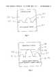
- a buffer layer designuses strained superlattices to bend threading dislocations.
- a buffer layer 21joins a strained superlattice 22 to a substrate 20 .
- a buffer layer 23joins a strained superlattice 24 to strained superlattice 22 .
- a device epitaxial layer 25is grown on top of strained superlattice 24 .
- a threading dislocation 26shows a dislocation section 27 bent by superlattice 22 and a dislocation section 28 bent by superlattice 24 .
- the effectiveness of the strained superlattice approachis limited by its narrow stressed region.
- the bending moment of the threading dislocationhas to be very large, or equivalently, the radius of curvature of the dislocation has to be comparable to the thickness of the superlattice, typically only a few hundred Angstroms. If the dislocation can not be confined to the narrow region of the superlattice, it will propagate through the superlattice region. With a limited number of superlattice regions that one can use, the approach of a strained superlattice can only reduce the number of threading dislocations while not completely eliminating them.
- a compliant substratecan be viewed as a relatively “energetically unstable” template.
- the stressis relaxed through elastic or plastic deformation of the template.
- the templatemay sacrifice itself as a sink of all the dislocations, to preserve the quality of the epitaxial layer.
- the substrateapplies a “long range” stress field to the heteroepitaxial layer to constrain dislocations.
- the “sign” of the applied stress field, tension or compression,is often determined by the relative thermal expansion coefficients between the epitaxial layer and the substrate since thermal stress is the most controllable means to provide the long range stress. If the thermal expansion of the epitaxial layer is greater than the substrate and the temperature is higher than the epitaxial growth temperature, the applied stress should be compressive; otherwise, the stress should be tensile.
- the stress-engineered substrate approachis different because the stress field exists throughout the entire heteroepitaxial layer, independent of the thickness of the epitaxial layer.
- the stress field in the strained superlatticeonly exists in the superlattice region, thus limiting its effectiveness in dislocation confinement.
- thermal stress originating from different thermal expansion coefficients between the epitaxial layers and the substrateis the most effective mechanism.
- thermal stressthe “sign” of stress will be reversed when the material temperature varies from higher than to lower than the epitaxial growth temperature at which the thermal stress is zero.
- the thermal stresscan confine dislocations at high temperatures, the stress from the very source can “unleash” the confined dislocations at low temperatures.
- multi-layer substratesthat can dynamically adjust the stress over different temperatures were designed.
- This inventiondiscusses new solutions to the problem for stress control over a wide range of temperatures.
- the basic concept of dislocation filteringis similar to that of the stress-engineered substrates, but the invention combines the design of substrates, epitaxial layer structures, and growth parameters to more easily and effectively confine dislocations at all temperatures.
- the layer structure, substrate structure, and growth parametersWith proper choices of the layer structure, substrate structure, and growth parameters, one can form low defect density epitaxial layers on lattice-mismatched substrates. Through interactions between dislocations and the stress field in the epitaxial layer, dislocations can be most effectively confined following the design of this invention.
- the design conceptcan be applied to any heteroepitaxial material systems as long as enough information about the dislocation structures in the epitaxial layers is available.
- a method for forming low defect density epitaxial layers on lattice-mismatched substratesincludes confining dislocations through interactions between the dislocations and the stress field in the epitaxial layer. This method is applicable to any heteroepitaxial material systems with any degree of lattice mismatch.
- the methodincludes choosing the desired epilayer and the top substrate layer for epitaxial growth, determining the lattice constant and thermal expansion coefficient of the final epilayer and the top substrate layer, bonding an additional substrate layer under the top substrate layer to form a composite substrate so that the desired epilayer has negative (positive) or zero thermal mismatch to the composite substrate if the lattice mismatch between the epilayer and the top substrate layer is positive (negative), and choosing a buffer layer to be deposited before the desired epilayer which is lattice matched to the epilayer.
- the chosen buffer layershould have a positive (negative) thermal mismatch to the entire substrate if the lattice mismatch is also positive (negative).
- a method for forming low defect density epitaxial layers on lattice-mismatched substratesincludes (a) choosing a first epilayer and a top substrate layer for epitaxial growth; (b) determining a first lattice constant and a first thermal expansion coefficient of the first epilayer; (c) determining a second lattice constant and a second thermal expansion coefficient of the top substrate layer; (d) bonding an additional substrate layer to the top substrate layer to form a composite substrate so that the first epilayer has either positive lattice mismatch and negative or zero thermal mismatch to the composite substrate, or negative lattice mismatch and positive thermal mismatch to the composite substrate; and (e) choosing a buffer layer which is lattice matched to the first epilayer to be deposited on the composite substrate before depositing the first epilayer, wherein (i) the buffer layer has positive thermal mismatch to the composite substrate when the buffer layer and the top substrate layer have positive lattice mismatch, and (ii) the buffer
- FIG. 1shows an example of the prior art of using a graded lattice constant buffer layer to reduce threading dislocations where the lattice constant of the buffer layer varies from the value of the substrate to the value of the desired epitaxial layer.
- FIG. 2shows an example of the prior art of using multiple strained superlattice regions to bend threading dislocations.
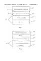
- FIG. 3shows an example of the prior art of using stress-engineered substrate to achieve a high-quality heteroepitaxial layer.
- FIG. 4shows a schematic illustration of the invention in which the substrate includes a single type of material or more than one type of material (composite substrate) in order to achieve the desired thermal expansion coefficient, where the dislocation confining buffer layer and the final epitaxial layer have the same lattice constant.
- FIG. 5shows a schematic of the visible LED (AlInGaP) layers grown on a lattice-mismatched, transparent composite substrate made of GaP and InP.
- FIG. 6shows a schematic of InP-based epitaxial layers grown on a lattice-mismatched composite substrate made of Si and Ge.
- Ris the bending radius (radius of bending curvature)
- ⁇is between 0.5 and 1
- Gis the shear modulus
- bis the length of the Burgers vector
- ⁇is the shear stress in the dislocation glide plane resolved in the direction of b.
- the Burgers vector of most threading dislocationsis known, that is, they are either 60-degree dislocations or partial dislocations.
- the knowledge of the possible Burgers vectors and magnitude of stressallows us to calculate the “worst case” or the “largest possible” radius of bending curvature for dislocations. Those dislocations that are bent downward may recombine and form loops at the growth interface or terminate themselves at the boundaries of the wafer.
- the heteroepitaxial layershould be dislocation free in principle as shown in FIG. 3.
- the stress-engineered substratesconsisting of more than two materials are often needed.
- the stress-engineered substratesmay consist of multilayers including GaP, Si, a thin joining layer with a low melting-point, and Ge.
- the complicated process and use of multiple substrate layers to form a stress-engineered substratemay increase the cost and reduce the product yield.
- Our new substrate/epilayer co-design processcan be summarized in the following steps:
- [0036](4) choose a buffer layer to be deposited before the desired epilayer which is lattice matched to the epilayer. Furthermore, the chosen buffer layer should have a positive (negative) thermal mismatch to the entire substrate if the lattice mismatch is also positive (negative).
- Steps (1) to (4)outline the procedure for co-design of the substrate and buffer layer. After the substrate and buffer layer structures are decided, the following growth procedure is preferred:
- dislocations 41 , 42 , 43are confined through interactions between dislocations 41 , 42 , 43 and thermal stress during thermal annealing of buffer layer 44 .
- the reversed sign of the thermal stress in buffer layer 44may unleash the originally confined dislocations.
- the dislocation unleashing forcevanishes at an epi/buffer interface 45 and turns into a dislocation confinement force in the epitaxial layer region, those unleashed dislocations can at most reach interface 45 between epilayer 46 and buffer layer 44 . If substrate 47 satisfies the necessary conditions without being formed as a composite substrate, then there is no need to bond an additional substrate layer on its bottom.
- AlInGaP compound semiconductor materialis the primary material for making red/orange/yellow light-emitting diodes (LEDs).
- LEDsred/orange/yellow light-emitting diodes
- the materialis grown epitaxially on a lattice-matched GaAs substrate. Because the GaAs substrate is opaque to visible light, most of the light generated by AlInGaP compounds is absorbed by the substrate, which significantly reduces the brightness of the LED. It would be ideal if the AlInGaP layers were grown directly on a transparent GaP substrate, but the 4% lattice mismatch between the epilayer and GaP makes that nearly impossible. This problem can be solved using our invented method.
- an InP substrate 51is first bonded to a backside of a GaP substrate 52 to adjust the overall thermal expansion coefficient of a composite substrate 53 .
- a high Al-content AlGaAs buffer layer 54which is lattice matched to a desired AlInGaP layer 55 is grown on GaP substrate 52 , followed by high temperature (e.g., 900° C.) annealing.
- AlGaAs layer 54has a larger thermal expansion coefficient than the GaP/InP composite substrate 53 , AlGaAs layer 54 is under compression at the annealing temperature. With a 4% positive lattice mismatch, the dislocations (not shown) in AlGaAs layer 54 are bent towards an Al GaAs/GaP interface 56 through the dislocation/stress interaction.
- the desired AlInGaP LED layers 55are grown.
- the thermal stress in AlGaAs layer 54is reversed from compression to tension, causing possible dislocation unleashing.
- the unleashed dislocationsmay terminate at an AlInGaP/AlGaAs interface 57 since AlInGaP layer 55 is thermally matched to composite GaP/InP substrate 53 so the dislocation unleashing stress vanishes in AlInGaP layer 55 .
- AlInGaP epilayer 55may even be slightly under compression at lower than the growth temperature, thus making dislocations in AlGaAs buffer layer 54 even more unlikely to penetrate into AlInGaP layer 55 .
- our techniquecan not only produce high brightness red/orange/yellow AlInGaP LEDs on GaP transparent substrates but also extend the color range of the LEDs to the yellow/green regime.
- the AlInGaP layers grown in our methodcan have different lattice constants than GaAs.
- the In compositioncan be adjusted from about 35% to 65% as long as the buffer layer is adjusted accordingly (e.g., using AlGaAsP or AlInGaAsP to replace AlGaAs as the buffer layer) to match the chosen AlInGaP compounds. This flexibility allows us to make high brightness yellow/green LEDs that are not available today.
- InP-based compound semiconductors on Si substratesoffers compelling advantages to optical and electronic devices such as solar cells, high-speed transistors, and infrared laser diodes.
- the cost of Si substrateis only about one thirtieth of the InP substrate, while the mechanical and thermal properties of Si wafers are far superior to InP wafers.
- InP-based electronic transistorssuch as heterojunction bipolar transistors (HBTs) and optical devices such as lasers, detectors, and optical modulators directly on Si facilitates integration of InP and Si devices.
- HBTsheterojunction bipolar transistors
- optical devicessuch as lasers, detectors, and optical modulators
- a composite substratefirst by bonding a Ge wafer (substrate) 61 to a backside of a Si wafer (substrate) 62 for adjustment of the thermal expansion coefficient of a composite substrate 63 .
- InAlAs or InGaAs buffer layers 64which are lattice matched to InP are grown on Si substrate 62 . Many dislocations are formed in these buffer layers due to the large positive lattice mismatch to Si.
- High temperature thermal annealingis then conducted after growth of each InAlAs or InGaAs buffer layer 64 .
- buffer layer 64The positive thermal mismatch between buffer layer 64 and composite substrate 63 creates a compressive stress in the buffer layer, which bends the dislocations (not shown) downward.
- InP epitaxial layer 65After repeating the buffer layer growth and thermal annealing process several times, we grow an InP epitaxial layer 65 . Finally, InP-based compound device layers 66 are grown on top InP layer 65 .
- InP layer 65is thick enough (e.g., 2 ⁇ m) to isolate the stress effect from the top device layers 66 .
- the above discussionassumes that one wants to grow InP-based material on the Si-side of the Si/Ge composite wafer. It is also possible to grow the same structure on the Ge-side of such a wafer. In fact, two advantages of growing InP-based materials on the Ge-side of the wafer are a smaller lattice mismatch (3.7% as opposed to 7.7%) and the availability of an initial defect-free GaAs buffer layer on Ge. As a result, all InP-based epilayers may be grown on a GaAs buffer layer for better nucleation and fewer antiphase domain problems.
- InP-based materialshave the same lattice constant of InP (i.e., lattice matched), it does not have to be so.
- the invented techniqueapplies as well to materials containing In or P but not necessarily matched to InP.
- InGaAsP or InGaAlAs quaternary compounds with lattice constants 1 to 2% smaller or greater than InPcan also be grown on the Si/Ge substrate using the disclosed technique.
- Sb-based semiconductorssuch as GaSb, InSb, or InGaSbAs, etc.
- N-based semiconductorsincluding (In)GaN, AlGaN, AlN, BN, etc.
- As-based semiconductorsincluding N-doped GaAs, InGaAs, etc.
- II-VI compound semiconductorssuch as ZnSe
- Si-based semiconductorssuch as SiGe and C-doped SiGe
- C-based semiconductorssuch as SiC, and so on.
Landscapes
- Engineering & Computer Science (AREA)
- Physics & Mathematics (AREA)
- Condensed Matter Physics & Semiconductors (AREA)
- General Physics & Mathematics (AREA)
- Manufacturing & Machinery (AREA)
- Computer Hardware Design (AREA)
- Microelectronics & Electronic Packaging (AREA)
- Power Engineering (AREA)
- Chemical & Material Sciences (AREA)
- Materials Engineering (AREA)
- Recrystallisation Techniques (AREA)
Abstract
Description
- The invention pertains to the field of semiconductor design. More particularly, the invention pertains to ensuring high-quality epitaxial growth on lattice mismatched substrates.[0001]
- Many advanced semiconductor electronic and optoelectronic devices are made of epitaxial layers. A critical condition for obtaining high quality epitaxial layers is that the lattice constant of the epilayers has to be equal to that of the substrate. Even with a lattice mismatch as small as 1%, the density of defects in the epilayers can rise drastically when the epitaxial layers are thicker than a few hundred Angstroms. Over the years, the requirement of lattice match has severely limited the advance of semiconductor device technologies. Device performance is often compromised because the optimal epitaxial materials do not happen to have the same lattice constant as the substrate. As mixed-signal circuits and heterogeneously integrated systems-on-a-chip become the trend for future microelectronics, the inability to grow high-quality epitaxial layers on lattice-mismatched substrates (e.g., growing InP on Si) has made this development difficult and costly. In fact, forming high-quality epitaxial layers on lattice-mismatched substrates has been and will continue to be the foremost challenge for semiconductor material research.[0002]
- Threading dislocations are the primary defects in the heteroepitaxial layers, although other types of defects such as stacking faults, micro twins, and anti-phase domains may also exist. To cope with the problem of threading dislocations, two approaches have been developed: one focusing on the epitaxial growth and the other focusing on the substrate design. Among the popular techniques in the first approach are the growth of buffer layers and growth on small mesas; and the techniques in the second approach include compliant substrates and stress-engineered substrates. Our invention, the co-design of the substrate and epitaxial layers, combines the merits of both approaches without the drawbacks of each. To appreciate the inherent merits of the new method, let us briefly review the existing approaches first.[0003]
- Referring to FIG. 1, one popular buffer layer design uses a strain-graded buffered[0004]
layer 12 to gradually transform the lattice constant from the value of thesubstrate 10 to the final desired value ofepitaxial layer 14. - Referring to FIG. 2, another buffer layer design uses strained superlattices to bend threading dislocations. A[0005]
buffer layer 21 joins a strained superlattice22 to asubstrate 20. Abuffer layer 23 joins a strained superlattice24 to strained superlattice22. A deviceepitaxial layer 25 is grown on top of strained superlattice24. A threading dislocation26 shows adislocation section 27 bent by superlattice22 and adislocation section 28 bent by superlattice24. - These two approaches can be used jointly with the technique of mesa growth so that threading dislocations may either be bent or annihilated in the superlattice regions or be terminated at the periphery of the mesas. Although the strained superlattice and mesa growth methods have proved to be effective in reducing the number of threading dislocations, there still exist an appreciable amount of threading dislocations in the epilayers, severe enough to degrade the device performance and reliability. The effectiveness of the mesa growth is limited by the achievable mesa size. The first approach is most effective only when the mesa size is smaller than the epitaxial layer thickness. However, this condition can rarely be satisfied in practice. On the other hand, the effectiveness of the strained superlattice approach is limited by its narrow stressed region. To bend a threading dislocation to the plane of superlattice, the bending moment of the threading dislocation has to be very large, or equivalently, the radius of curvature of the dislocation has to be comparable to the thickness of the superlattice, typically only a few hundred Angstroms. If the dislocation can not be confined to the narrow region of the superlattice, it will propagate through the superlattice region. With a limited number of superlattice regions that one can use, the approach of a strained superlattice can only reduce the number of threading dislocations while not completely eliminating them.[0006]
- The approaches of compliant substrates and stress-engineered substrates are based on a different principle from the previous approaches. A compliant substrate can be viewed as a relatively “energetically unstable” template. When stress is applied to the template by the heteroepitaxial layer, the stress is relaxed through elastic or plastic deformation of the template. As a result, the template may sacrifice itself as a sink of all the dislocations, to preserve the quality of the epitaxial layer. For stress-engineered substrates, the substrate applies a “long range” stress field to the heteroepitaxial layer to constrain dislocations. The “sign” of the applied stress field, tension or compression, is often determined by the relative thermal expansion coefficients between the epitaxial layer and the substrate since thermal stress is the most controllable means to provide the long range stress. If the thermal expansion of the epitaxial layer is greater than the substrate and the temperature is higher than the epitaxial growth temperature, the applied stress should be compressive; otherwise, the stress should be tensile.[0007]
- Although the previously mentioned superlattice approach also uses stress to confine threading dislocations, the stress-engineered substrate approach is different because the stress field exists throughout the entire heteroepitaxial layer, independent of the thickness of the epitaxial layer. In contrast, the stress field in the strained superlattice only exists in the superlattice region, thus limiting its effectiveness in dislocation confinement. To create such a long range stress, thermal stress originating from different thermal expansion coefficients between the epitaxial layers and the substrate is the most effective mechanism.[0008]
- However, one problem associated with thermal stress is that the “sign” of stress will be reversed when the material temperature varies from higher than to lower than the epitaxial growth temperature at which the thermal stress is zero. In other words, if the thermal stress can confine dislocations at high temperatures, the stress from the very source can “unleash” the confined dislocations at low temperatures. To overcome this problem, multi-layer substrates that can dynamically adjust the stress over different temperatures were designed. Although these designs of stress-engineered substrates solve the thermal stress sign reversal problems, they increase the substrate cost and process complexity.[0009]
- This invention discusses new solutions to the problem for stress control over a wide range of temperatures. The basic concept of dislocation filtering is similar to that of the stress-engineered substrates, but the invention combines the design of substrates, epitaxial layer structures, and growth parameters to more easily and effectively confine dislocations at all temperatures. With proper choices of the layer structure, substrate structure, and growth parameters, one can form low defect density epitaxial layers on lattice-mismatched substrates. Through interactions between dislocations and the stress field in the epitaxial layer, dislocations can be most effectively confined following the design of this invention. The design concept can be applied to any heteroepitaxial material systems as long as enough information about the dislocation structures in the epitaxial layers is available.[0010]
- Briefly stated, a method for forming low defect density epitaxial layers on lattice-mismatched substrates includes confining dislocations through interactions between the dislocations and the stress field in the epitaxial layer. This method is applicable to any heteroepitaxial material systems with any degree of lattice mismatch. The method includes choosing the desired epilayer and the top substrate layer for epitaxial growth, determining the lattice constant and thermal expansion coefficient of the final epilayer and the top substrate layer, bonding an additional substrate layer under the top substrate layer to form a composite substrate so that the desired epilayer has negative (positive) or zero thermal mismatch to the composite substrate if the lattice mismatch between the epilayer and the top substrate layer is positive (negative), and choosing a buffer layer to be deposited before the desired epilayer which is lattice matched to the epilayer. The chosen buffer layer should have a positive (negative) thermal mismatch to the entire substrate if the lattice mismatch is also positive (negative).[0011]
- According to an embodiment of the invention, a method for forming low defect density epitaxial layers on lattice-mismatched substrates includes (a) choosing a first epilayer and a top substrate layer for epitaxial growth; (b) determining a first lattice constant and a first thermal expansion coefficient of the first epilayer; (c) determining a second lattice constant and a second thermal expansion coefficient of the top substrate layer; (d) bonding an additional substrate layer to the top substrate layer to form a composite substrate so that the first epilayer has either positive lattice mismatch and negative or zero thermal mismatch to the composite substrate, or negative lattice mismatch and positive thermal mismatch to the composite substrate; and (e) choosing a buffer layer which is lattice matched to the first epilayer to be deposited on the composite substrate before depositing the first epilayer, wherein (i) the buffer layer has positive thermal mismatch to the composite substrate when the buffer layer and the top substrate layer have positive lattice mismatch, and (ii) the buffer layer has negative thermal mismatch to the composite substrate when the buffer layer and the top substrate layer have negative lattice mismatch.[0012]
- FIG. 1 shows an example of the prior art of using a graded lattice constant buffer layer to reduce threading dislocations where the lattice constant of the buffer layer varies from the value of the substrate to the value of the desired epitaxial layer.[0013]
- FIG. 2 shows an example of the prior art of using multiple strained superlattice regions to bend threading dislocations.[0014]
- FIG. 3 shows an example of the prior art of using stress-engineered substrate to achieve a high-quality heteroepitaxial layer.[0015]
- FIG. 4 shows a schematic illustration of the invention in which the substrate includes a single type of material or more than one type of material (composite substrate) in order to achieve the desired thermal expansion coefficient, where the dislocation confining buffer layer and the final epitaxial layer have the same lattice constant.[0016]
- FIG. 5 shows a schematic of the visible LED (AlInGaP) layers grown on a lattice-mismatched, transparent composite substrate made of GaP and InP.[0017]
- FIG. 6 shows a schematic of InP-based epitaxial layers grown on a lattice-mismatched composite substrate made of Si and Ge.[0018]
- Referring to FIG. 3, assuming for illustration purposes that an epilayer (epitaxial layer)[0019]30 has a larger lattice constant than a
substrate 31 on which epilayer30 is directly grown, thenthreading dislocations - R=αGb/τ (1)
- where R is the bending radius (radius of bending curvature), α is between 0.5 and 1, G is the shear modulus, b is the length of the Burgers vector, and τ is the shear stress in the dislocation glide plane resolved in the direction of b. Assuming the following typical numbers of α=1, b=4 Å, G=10[0020]11dynes/cm2, and t=108dynes/cm2, the radius of bending curvature, R, is 0.4 μm. The above calculation is approximate because it assumes the material has zero Poisson ratio, i.e., that the energy for screw and edge dislocations are the same. For a given lattice structure of the heteroepitaxial layer such as the popular zinc blende structure, the Burgers vector of most threading dislocations is known, that is, they are either 60-degree dislocations or partial dislocations. The knowledge of the possible Burgers vectors and magnitude of stress allows us to calculate the “worst case” or the “largest possible” radius of bending curvature for dislocations. Those dislocations that are bent downward may recombine and form loops at the growth interface or terminate themselves at the boundaries of the wafer. Hence when the epitaxial layer thickness is substantially greater than the “worst case” bending radius, the heteroepitaxial layer should be dislocation free in principle as shown in FIG. 3.
- Once the lattice constant between the epitaxial layer and the substrate is determined, one can choose other materials of proper thermal expansion coefficients to form a composite substrate and proper epitaxial buffer layers most favorable to dislocation confinement. The methods of choosing the substrate materials have been discussed in great detail in the previous invention on stress-engineered substrates filed on Dec. 11, 1998 as U.S. application Ser. No. 09/210,166 incorporated herein by reference. For reference purposes, we summarize the design principles of stress-engineered substrates as contained therein:[0021]
- (1) choose the materials for the epitaxial layers and the top layer of the substrate,[0022]
- (2) compare their lattice constants and thermal expansion coefficients,[0023]
- (3) if the epilayer has a larger lattice constant (positive lattice mismatch) and a larger thermal expansion coefficient (positive thermal mismatch) than the top substrate layer, bond a low thermal-expansion layer at the bottom of the substrate, and[0024]
- (4) ensure that the bonded substrate layer does not significantly affect the overall thermal expansion coefficient of the substrate at a higher than the epi-growth temperature, but makes the overall thermal expansion coefficient of the substrate less than or equal to that of the epilayer at lower than the epi-growth temperature.[0025]
- If principle (3) is reversed, that is, if there is negative lattice and thermal mismatch, then principle (4) becomes[0026]
- (4a) ensure that the bonded substrate layer does not significantly affect the overall thermal expansion coefficient of the substrate at a higher than the epi-growth temperature, but makes the overall thermal expansion coefficient of the substrate greater than that of the epilayer at lower than the epi-growth temperature.[0027]
- If only the lattice constant relation in principle (3) is reversed, then principle (4) becomes[0028]
- (4b) ensure that the bonded substrate layer makes the overall thermal expansion coefficient greater than that of the epilayer at higher than the epi-growth temperature, but does not significantly affect the overall substrate thermal expansion coefficient at lower than the epi-growth temperature.[0029]
- If only the thermal expansion coefficient relation in principle (3) is reversed, then principle (4) becomes[0030]
- (4c) ensure that the bonded substrate layer makes the overall thermal expansion coefficient of the substrate less than that of the epilayer at higher than the epi-growth temperature, but does not significantly affect the overall substrate thermal expansion coefficient at lower than the epi-growth temperature.[0031]
- In practice, it is not always easy to satisfy the above criteria. Particularly in the last two situations outlined above, stress-engineered substrates consisting of more than two materials are often needed. For example, should one want to grow AlInGaP on GaP substrates to make red, orange and yellow LEDs, the stress-engineered substrates may consist of multilayers including GaP, Si, a thin joining layer with a low melting-point, and Ge. The complicated process and use of multiple substrate layers to form a stress-engineered substrate may increase the cost and reduce the product yield. In this invention, we make use of the flexibility of selecting epitaxial buffer layers to simplify the substrate design. Our new substrate/epilayer co-design process can be summarized in the following steps:[0032]
- (1) choose the desired epilayer and the top substrate layer for epitaxial growth,[0033]
- (2) determine the lattice constant and thermal expansion coefficient of the final epilayer and the top substrate layer,[0034]
- (3) if necessary, bond an additional substrate layer under the top substrate layer to form a composite substrate so that the desired epilayer has positive (negative) lattice mismatch and negative (positive) or zero thermal mismatch to the substrate, and[0035]
- (4) choose a buffer layer to be deposited before the desired epilayer which is lattice matched to the epilayer. Furthermore, the chosen buffer layer should have a positive (negative) thermal mismatch to the entire substrate if the lattice mismatch is also positive (negative).[0036]
- Steps (1) to (4) outline the procedure for co-design of the substrate and buffer layer. After the substrate and buffer layer structures are decided, the following growth procedure is preferred:[0037]
- (1) grow the buffer layer on the substrate synthesized according to the above design,[0038]
- (2) when the buffer layer reaches the thickness of the bending radius of most threading dislocations, perform thermal annealing (typically a few hundred degrees higher than the growth temperature),[0039]
- (3) grow another buffer layer and anneal again, repeating the growth and annealing process several times until the aggregate buffer layer thickness is well above the “worst case” dislocation bending radius, and[0040]
- (4) grow the desired epilayers for device applications.[0041]
- Using the new design and growth procedure, one can simplify the substrate design because the confined dislocations in the buffer layer can not penetrate the epilayer/buffer layer interface.[0042]
- Referring to FIG. 4, after a[0043]
buffer layer 44 is grown on asubstrate 47,dislocations dislocations buffer layer 44. When the material temperature falls below the growth temperature, the reversed sign of the thermal stress inbuffer layer 44 may unleash the originally confined dislocations. However, since the dislocation unleashing force vanishes at an epi/buffer interface 45 and turns into a dislocation confinement force in the epitaxial layer region, those unleashed dislocations can atmost reach interface 45 betweenepilayer 46 andbuffer layer 44. Ifsubstrate 47 satisfies the necessary conditions without being formed as a composite substrate, then there is no need to bond an additional substrate layer on its bottom. - Growth of AlInGaP Visible LEDs on Transparent GaP Substrates[0044]
- AlInGaP compound semiconductor material is the primary material for making red/orange/yellow light-emitting diodes (LEDs). Today, the material is grown epitaxially on a lattice-matched GaAs substrate. Because the GaAs substrate is opaque to visible light, most of the light generated by AlInGaP compounds is absorbed by the substrate, which significantly reduces the brightness of the LED. It would be ideal if the AlInGaP layers were grown directly on a transparent GaP substrate, but the 4% lattice mismatch between the epilayer and GaP makes that nearly impossible. This problem can be solved using our invented method.[0045]
- Referring to FIG. 5, an[0046]
InP substrate 51 is first bonded to a backside of aGaP substrate 52 to adjust the overall thermal expansion coefficient of acomposite substrate 53. After some necessary epitaxial buffer layers (not shown) usually needed to establish the surface conditions for epitaxial growth, a high Al-contentAlGaAs buffer layer 54 which is lattice matched to a desiredAlInGaP layer 55 is grown onGaP substrate 52, followed by high temperature (e.g., 900° C.) annealing. BecauseAlGaAs layer 54 has a larger thermal expansion coefficient than the GaP/InPcomposite substrate 53,AlGaAs layer 54 is under compression at the annealing temperature. With a 4% positive lattice mismatch, the dislocations (not shown) inAlGaAs layer 54 are bent towards an Al GaAs/GaP interface 56 through the dislocation/stress interaction. - After repeating the AlGaAs buffer layer growth and annealing process a few times so that the aggregate AlGaAs layer thickness is well above the worst case dislocation bending radius, the desired AlInGaP LED layers[0047]55 are grown. During sample cooling, the thermal stress in
AlGaAs layer 54 is reversed from compression to tension, causing possible dislocation unleashing. However, the unleashed dislocations may terminate at an AlInGaP/AlGaAs interface 57 sinceAlInGaP layer 55 is thermally matched to composite GaP/InP substrate 53 so the dislocation unleashing stress vanishes inAlInGaP layer 55. If we choose the GaP to InP thickness ratio greater than one,AlInGaP epilayer 55 may even be slightly under compression at lower than the growth temperature, thus making dislocations inAlGaAs buffer layer 54 even more unlikely to penetrate intoAlInGaP layer 55. - Finally, our technique can not only produce high brightness red/orange/yellow AlInGaP LEDs on GaP transparent substrates but also extend the color range of the LEDs to the yellow/green regime. Unlike the conventional approach where the AlInGaP layers have to be lattice matched to GaAs, the AlInGaP layers grown in our method can have different lattice constants than GaAs. In other words, the In composition can be adjusted from about 35% to 65% as long as the buffer layer is adjusted accordingly (e.g., using AlGaAsP or AlInGaAsP to replace AlGaAs as the buffer layer) to match the chosen AlInGaP compounds. This flexibility allows us to make high brightness yellow/green LEDs that are not available today.[0048]
- Growth of InP on Si or Ge for Solar Cells, High-speed Transistors, and Laser Diodes.[0049]
- Growing high quality InP-based compound semiconductors on Si substrates offers compelling advantages to optical and electronic devices such as solar cells, high-speed transistors, and infrared laser diodes. The cost of Si substrate is only about one thirtieth of the InP substrate, while the mechanical and thermal properties of Si wafers are far superior to InP wafers. In addition, growing InP-based electronic transistors such as heterojunction bipolar transistors (HBTs) and optical devices such as lasers, detectors, and optical modulators directly on Si facilitates integration of InP and Si devices. The main difficulty with InP-on-Si heteroepitaxial growth is again in the 7.7% positive lattice mismatch between the materials.[0050]
- Referring to FIG. 6, using the invented method, we can form a composite substrate first by bonding a Ge wafer (substrate)[0051]61 to a backside of a Si wafer (substrate)62 for adjustment of the thermal expansion coefficient of a
composite substrate 63. After standard buffer layer growth onSi substrate 62, InAlAs or InGaAs buffer layers64 which are lattice matched to InP are grown onSi substrate 62. Many dislocations are formed in these buffer layers due to the large positive lattice mismatch to Si. High temperature thermal annealing is then conducted after growth of each InAlAs orInGaAs buffer layer 64. The positive thermal mismatch betweenbuffer layer 64 andcomposite substrate 63 creates a compressive stress in the buffer layer, which bends the dislocations (not shown) downward. After repeating the buffer layer growth and thermal annealing process several times, we grow anInP epitaxial layer 65. Finally, InP-based compound device layers66 are grown ontop InP layer 65. - During sample cooling, the sign reversal of the thermal stress in InAlAs/[0052]
InGaAs buffer layer 64 may unleash the dislocations. However, those unleashed dislocations can not propagate throughInP layer 65 becauseInP layer 65 has zero stress or compressive stress at lower than the growth temperature due to its equal or smaller thermal expansion coefficient difference from the composite Si/Ge substrate 63. If dislocations can not penetrateInP layer 65, they can not enter the device epitaxial layers66 on top ofInP layer 65. - This statement is particularly true when[0053]
InP layer 65 is thick enough (e.g., 2 μm) to isolate the stress effect from the top device layers66. The above discussion assumes that one wants to grow InP-based material on the Si-side of the Si/Ge composite wafer. It is also possible to grow the same structure on the Ge-side of such a wafer. In fact, two advantages of growing InP-based materials on the Ge-side of the wafer are a smaller lattice mismatch (3.7% as opposed to 7.7%) and the availability of an initial defect-free GaAs buffer layer on Ge. As a result, all InP-based epilayers may be grown on a GaAs buffer layer for better nucleation and fewer antiphase domain problems. It should also be noted that although we have referred to InP-based materials as having the same lattice constant of InP (i.e., lattice matched), it does not have to be so. The invented technique applies as well to materials containing In or P but not necessarily matched to InP. For example, InGaAsP or InGaAlAs quaternary compounds withlattice constants 1 to 2% smaller or greater than InP can also be grown on the Si/Ge substrate using the disclosed technique. - Furthermore, the same principle can be applied to many other material systems including Sb-based semiconductors such as GaSb, InSb, or InGaSbAs, etc., N-based semiconductors including (In)GaN, AlGaN, AlN, BN, etc., As-based semiconductors including N-doped GaAs, InGaAs, etc., II-VI compound semiconductors such as ZnSe, Si-based semiconductors such as SiGe and C-doped SiGe, C-based semiconductors such as SiC, and so on.[0054]
- Accordingly, it is to be understood that the embodiments of the invention herein described are merely illustrative of the application of the principles of the invention. Reference herein to details of the illustrated embodiments are not intended to limit the scope of the claims, which themselves recite those features regarded as essential to the invention.[0055]
Claims (17)
1. A method for forming low defect density epitaxial layers on lattice-mismatched substrates, comprising the steps of:
a) choosing a first epilayer and a top substrate layer for epitaxial growth;
b) determining a first lattice constant and a first thermal expansion coefficient of said first epilayer;
c) determining a second lattice constant and a second thermal expansion coefficient of said top substrate layer;
d) bonding an additional substrate layer to said top substrate layer to form a composite substrate so that said first epilayer has either positive lattice mismatch and negative or zero thermal mismatch to said composite substrate, or negative lattice mismatch and positive or zero thermal mismatch to said composite substrate; and
e) choosing a buffer layer which is lattice matched to said first epilayer to be deposited on said composite substrate before depositing said first epilayer, wherein
said buffer layer has positive thermal mismatch to said composite substrate when said buffer layer and said top substrate layer have positive lattice mismatch, and
said buffer layer has negative thermal mismatch to said composite substrate when said buffer layer and said top substrate layer have negative lattice mismatch.
2. A method according to
claim 1
growing said buffer layer on said composite substrate;
thermally annealing said buffer layer and composite substrate when said buffer layer reaches a thickness of a bending radius of at least a majority of threading dislocations present in said buffer layer; and
repeating the steps of growing and thermally annealing until an aggregate buffer layer thickness is above said bending radius of all threading dislocations present in said buffer layer.
3. A method according to
claim 2
4. A method according to
claim 2
5. A method according to
claim 2
6. A method according to
claim 5
7. A method according to
claim 1
8. A method according to
claim 7
9. A method according to
claim 8
10. A method according to
claim 9
11. A method according to
claim 10
12. A method for forming low defect density epitaxial layers on lattice-mismatched substrates, comprising the steps of:
a) choosing a first epilayer and a substrate for epitaxial growth;
b) determining a first lattice constant and a first thermal expansion coefficient of said first epilayer;
c) determining a second lattice constant and a second thermal expansion coefficient of said substrate;
d) ensuring that said first epilayer has either positive lattice mismatch and negative or zero thermal mismatch to said substrate, or negative lattice mismatch and positive or zero thermal mismatch to said substrate; and
e) choosing a buffer layer which is lattice matched to said first epilayer to be deposited on said substrate before depositing said first epilayer, wherein
said buffer layer has positive thermal mismatch to said substrate when said buffer layer and said substrate have positive lattice mismatch, and
said buffer layer has negative thermal mismatch to said substrate when said buffer layer and said substrate have negative lattice mismatch.
13. A method according to
claim 12
growing said buffer layer on said substrate;
thermally annealing said buffer layer and substrate when said buffer layer reaches a thickness of a bending radius of at least a majority of threading dislocations present in said buffer layer; and
repeating the steps of growing and thermally annealing until an aggregate buffer layer thickness is above said bending radius of all threading dislocations present in said buffer layer.
14. A product made according to the method of
claim 1
15. A product made according to the method of
claim 2
16. A product made according to the method of
claim 12
17. A product made according to the method of
claim 13
Priority Applications (5)
| Application Number | Priority Date | Filing Date | Title |
|---|---|---|---|
| US09/247,413US20010042503A1 (en) | 1999-02-10 | 1999-02-10 | Method for design of epitaxial layer and substrate structures for high-quality epitaxial growth on lattice-mismatched substrates |
| PCT/US2000/003023WO2000048239A1 (en) | 1999-02-10 | 2000-02-04 | Heteroepitaxial growth with thermal expansion- and lattice-mismatch |
| JP2000599070AJP2002536844A (en) | 1999-02-10 | 2000-02-04 | Heteroepitaxial growth under thermal expansion and lattice mismatch |
| EP00910087AEP1155443A1 (en) | 1999-02-10 | 2000-02-04 | Heteroepitaxial growth with thermal expansion and lattice mismatch |
| TW089102083ATW494475B (en) | 1999-02-10 | 2000-03-28 | Method for design of epitaxial layer and substrate structures for high-quality epitaxial growth on lattice-mismatched substrates |
Applications Claiming Priority (1)
| Application Number | Priority Date | Filing Date | Title |
|---|---|---|---|
| US09/247,413US20010042503A1 (en) | 1999-02-10 | 1999-02-10 | Method for design of epitaxial layer and substrate structures for high-quality epitaxial growth on lattice-mismatched substrates |
Publications (1)
| Publication Number | Publication Date |
|---|---|
| US20010042503A1true US20010042503A1 (en) | 2001-11-22 |
Family
ID=22934831
Family Applications (1)
| Application Number | Title | Priority Date | Filing Date |
|---|---|---|---|
| US09/247,413AbandonedUS20010042503A1 (en) | 1999-02-10 | 1999-02-10 | Method for design of epitaxial layer and substrate structures for high-quality epitaxial growth on lattice-mismatched substrates |
Country Status (5)
| Country | Link |
|---|---|
| US (1) | US20010042503A1 (en) |
| EP (1) | EP1155443A1 (en) |
| JP (1) | JP2002536844A (en) |
| TW (1) | TW494475B (en) |
| WO (1) | WO2000048239A1 (en) |
Cited By (48)
| Publication number | Priority date | Publication date | Assignee | Title |
|---|---|---|---|---|
| US6617060B2 (en) | 2000-12-14 | 2003-09-09 | Nitronex Corporation | Gallium nitride materials and methods |
| US20050130424A1 (en)* | 2002-07-16 | 2005-06-16 | International Business Machines Corporation | Use of hydrogen implantation to improve material properties of silicon-germanium-on-insulator material made by thermal diffusion |
| US20050133818A1 (en)* | 2003-12-17 | 2005-06-23 | Johnson Jerry W. | Gallium nitride material devices including an electrode-defining layer and methods of forming the same |
| US20050145851A1 (en)* | 2003-12-17 | 2005-07-07 | Nitronex Corporation | Gallium nitride material structures including isolation regions and methods |
| US20050167775A1 (en)* | 2003-08-05 | 2005-08-04 | Nitronex Corporation | Gallium nitride material transistors and methods associated with the same |
| US20050285142A1 (en)* | 2004-06-28 | 2005-12-29 | Nitronex Corporation | Gallium nitride materials and methods associated with the same |
| US20050285155A1 (en)* | 2004-06-28 | 2005-12-29 | Nitronex Corporation | Semiconductor device-based sensors and methods associated with the same |
| US20060006500A1 (en)* | 2004-07-07 | 2006-01-12 | Nitronex Corporation | III-nitride materials including low dislocation densities and methods associated with the same |
| US20060214289A1 (en)* | 2004-10-28 | 2006-09-28 | Nitronex Corporation | Gallium nitride material-based monolithic microwave integrated circuits |
| US20060249748A1 (en)* | 2005-05-03 | 2006-11-09 | Nitronex Corporation | Gallium nitride material structures including substrates and methods associated with the same |
| US7247889B2 (en) | 2004-12-03 | 2007-07-24 | Nitronex Corporation | III-nitride material structures including silicon substrates |
| US20070187696A1 (en)* | 2004-03-29 | 2007-08-16 | Shigeya Naritsuka | Semiconductor light emitting device |
| US20070202360A1 (en)* | 2005-10-04 | 2007-08-30 | Nitronex Corporation | Gallium nitride material transistors and methods for wideband applications |
| US20070272957A1 (en)* | 2005-12-02 | 2007-11-29 | Nitronex Corporation | Gallium nitride material devices and associated methods |
| US20080026502A1 (en)* | 2005-05-31 | 2008-01-31 | The Regents Of The University Of California | Growth of non-polar m-plane iii-nitride film using metalorganic chemical vapor deposition (mocvd) |
| US20080035143A1 (en)* | 2006-08-14 | 2008-02-14 | Sievers Robert E | Human-powered dry powder inhaler and dry powder inhaler compositions |
| US20080113496A1 (en)* | 2006-11-15 | 2008-05-15 | The Regents Of The University Of California | METHOD FOR HETEROEPITAXIAL GROWTH OF HIGH-QUALITY N-FACE GaN, InN, AND AlN AND THEIR ALLOYS BY METAL ORGANIC CHEMICAL VAPOR DEPOSITION |
| US20080173895A1 (en)* | 2007-01-24 | 2008-07-24 | Sharp Laboratories Of America, Inc. | Gallium nitride on silicon with a thermal expansion transition buffer layer |
| CN100472749C (en)* | 2004-01-09 | 2009-03-25 | S.O.I.Tec绝缘体上硅技术公司 | Substrate with defined coefficient of thermal expansion |
| US7566913B2 (en) | 2005-12-02 | 2009-07-28 | Nitronex Corporation | Gallium nitride material devices including conductive regions and methods associated with the same |
| US20090194773A1 (en)* | 2008-02-05 | 2009-08-06 | Nitronex Corporation | Gallium nitride material devices including diamond regions and methods associated with the same |
| US20090224269A1 (en)* | 2008-03-10 | 2009-09-10 | Kabushiki Kaisha Toshiba | Semiconductor light emitting device and method for manufacturing same, and epitaxial wafer |
| US20090246944A1 (en)* | 2006-11-15 | 2009-10-01 | The Regents Of The University Of California | METHOD FOR HETEROEPITAXIAL GROWTH OF HIGH-QUALITY N-FACE GaN, InN, AND AlN AND THEIR ALLOYS BY METAL ORGANIC CHEMICAL VAPOR DEPOSITION |
| US20090267188A1 (en)* | 2008-04-29 | 2009-10-29 | Nitronex Corporation | Gallium nitride material processing and related device structures |
| US7655090B2 (en) | 2000-08-04 | 2010-02-02 | The Regents Of The University Of California | Method of controlling stress in gallium nitride films deposited on substrates |
| US20100116327A1 (en)* | 2008-11-10 | 2010-05-13 | Emcore Corporation | Four junction inverted metamorphic multijunction solar cell |
| US7745848B1 (en) | 2007-08-15 | 2010-06-29 | Nitronex Corporation | Gallium nitride material devices and thermal designs thereof |
| CN103066157A (en)* | 2013-01-07 | 2013-04-24 | 中国科学院上海微系统与信息技术研究所 | Method of reducing surface roughness of InP-base InGaAs heteroblastic material |
| US20140299872A1 (en)* | 2011-04-06 | 2014-10-09 | Isis Innovation Limited | Heterogeneous intergration of group iii-v or ii-vi materials with silicon or germanium |
| WO2014209390A1 (en)* | 2013-06-28 | 2014-12-31 | Intel Corporation | Selective epitaxially grown iii-v materials based devices |
| US20150061030A1 (en)* | 2013-08-29 | 2015-03-05 | Samsung Electronics Co., Ltd. | Semiconductor structure including metal silicide buffer layers and methods of fabricating the same |
| US9343874B2 (en)* | 2012-08-01 | 2016-05-17 | Ucl Business Plc | Semiconductor device and fabrication method |
| WO2016099494A1 (en)* | 2014-12-17 | 2016-06-23 | Intel Corporation | Integrated circuit die having reduced defect group iii-nitride layer and methods associated therewith |
| US9627473B2 (en) | 2015-09-08 | 2017-04-18 | Macom Technology Solutions Holdings, Inc. | Parasitic channel mitigation in III-nitride material semiconductor structures |
| US9673281B2 (en) | 2015-09-08 | 2017-06-06 | Macom Technology Solutions Holdings, Inc. | Parasitic channel mitigation using rare-earth oxide and/or rare-earth nitride diffusion barrier regions |
| US9704705B2 (en) | 2015-09-08 | 2017-07-11 | Macom Technology Solutions Holdings, Inc. | Parasitic channel mitigation via reaction with active species |
| US9773898B2 (en) | 2015-09-08 | 2017-09-26 | Macom Technology Solutions Holdings, Inc. | III-nitride semiconductor structures comprising spatially patterned implanted species |
| US9799520B2 (en) | 2015-09-08 | 2017-10-24 | Macom Technology Solutions Holdings, Inc. | Parasitic channel mitigation via back side implantation |
| US9806182B2 (en) | 2015-09-08 | 2017-10-31 | Macom Technology Solutions Holdings, Inc. | Parasitic channel mitigation using elemental diboride diffusion barrier regions |
| US9853107B2 (en) | 2014-03-28 | 2017-12-26 | Intel Corporation | Selective epitaxially grown III-V materials based devices |
| US10211294B2 (en) | 2015-09-08 | 2019-02-19 | Macom Technology Solutions Holdings, Inc. | III-nitride semiconductor structures comprising low atomic mass species |
| US11038023B2 (en) | 2018-07-19 | 2021-06-15 | Macom Technology Solutions Holdings, Inc. | III-nitride material semiconductor structures on conductive silicon substrates |
| RU2752291C2 (en)* | 2018-01-17 | 2021-07-26 | Интел Корпорейшн | Apparatuses based on selectively epitaxially grown iii-v group materials |
| US11264465B2 (en) | 2015-09-08 | 2022-03-01 | Macom Technology Solutions Holdings, Inc. | Parasitic channel mitigation using silicon carbide diffusion barrier regions |
| CN114300556A (en)* | 2021-12-30 | 2022-04-08 | 中国科学院苏州纳米技术与纳米仿生研究所 | Epitaxial structure, epitaxial growth method and optoelectronic device |
| US11935973B2 (en) | 2018-02-28 | 2024-03-19 | Asahi Kasei Microdevices Corporation | Infrared detecting device |
| US12057524B2 (en) | 2018-12-28 | 2024-08-06 | Epistar Corporation | Semiconductor stack, semiconductor device and method for manufacturing the same |
| EP4576165A1 (en)* | 2023-12-21 | 2025-06-25 | Imec VZW | A method for growing epitaxial layers on an engineered substrate |
Families Citing this family (44)
| Publication number | Priority date | Publication date | Assignee | Title |
|---|---|---|---|---|
| JP3535527B2 (en) | 1997-06-24 | 2004-06-07 | マサチューセッツ インスティテュート オブ テクノロジー | Controlling threading dislocations in germanium-on-silicon using graded GeSi layer and planarization |
| US7227176B2 (en) | 1998-04-10 | 2007-06-05 | Massachusetts Institute Of Technology | Etch stop layer system |
| JP2003520444A (en) | 2000-01-20 | 2003-07-02 | アンバーウェーブ システムズ コーポレイション | Low threading dislocation density lattice-mismatched epilayer that does not require high-temperature growth |
| US6750130B1 (en) | 2000-01-20 | 2004-06-15 | Amberwave Systems Corporation | Heterointegration of materials using deposition and bonding |
| US6602613B1 (en) | 2000-01-20 | 2003-08-05 | Amberwave Systems Corporation | Heterointegration of materials using deposition and bonding |
| US6392257B1 (en) | 2000-02-10 | 2002-05-21 | Motorola Inc. | Semiconductor structure, semiconductor device, communicating device, integrated circuit, and process for fabricating the same |
| JP2004503920A (en) | 2000-05-31 | 2004-02-05 | モトローラ・インコーポレイテッド | Semiconductor device and method of manufacturing the semiconductor device |
| WO2002009187A2 (en) | 2000-07-24 | 2002-01-31 | Motorola, Inc. | Heterojunction tunneling diodes and process for fabricating same |
| US6573126B2 (en) | 2000-08-16 | 2003-06-03 | Massachusetts Institute Of Technology | Process for producing semiconductor article using graded epitaxial growth |
| US6649480B2 (en) | 2000-12-04 | 2003-11-18 | Amberwave Systems Corporation | Method of fabricating CMOS inverter and integrated circuits utilizing strained silicon surface channel MOSFETs |
| US20020096683A1 (en) | 2001-01-19 | 2002-07-25 | Motorola, Inc. | Structure and method for fabricating GaN devices utilizing the formation of a compliant substrate |
| US6558973B2 (en)* | 2001-01-22 | 2003-05-06 | Honeywell International Inc. | Metamorphic long wavelength high-speed photodiode |
| US6703688B1 (en) | 2001-03-02 | 2004-03-09 | Amberwave Systems Corporation | Relaxed silicon germanium platform for high speed CMOS electronics and high speed analog circuits |
| WO2002082551A1 (en) | 2001-04-02 | 2002-10-17 | Motorola, Inc. | A semiconductor structure exhibiting reduced leakage current |
| WO2002082514A1 (en) | 2001-04-04 | 2002-10-17 | Massachusetts Institute Of Technology | A method for semiconductor device fabrication |
| US6992321B2 (en) | 2001-07-13 | 2006-01-31 | Motorola, Inc. | Structure and method for fabricating semiconductor structures and devices utilizing piezoelectric materials |
| US7019332B2 (en) | 2001-07-20 | 2006-03-28 | Freescale Semiconductor, Inc. | Fabrication of a wavelength locker within a semiconductor structure |
| US6855992B2 (en) | 2001-07-24 | 2005-02-15 | Motorola Inc. | Structure and method for fabricating configurable transistor devices utilizing the formation of a compliant substrate for materials used to form the same |
| US20030034491A1 (en) | 2001-08-14 | 2003-02-20 | Motorola, Inc. | Structure and method for fabricating semiconductor structures and devices for detecting an object |
| US6933518B2 (en) | 2001-09-24 | 2005-08-23 | Amberwave Systems Corporation | RF circuits including transistors having strained material layers |
| US20030071327A1 (en) | 2001-10-17 | 2003-04-17 | Motorola, Inc. | Method and apparatus utilizing monocrystalline insulator |
| WO2003079415A2 (en) | 2002-03-14 | 2003-09-25 | Amberwave Systems Corporation | Methods for fabricating strained layers on semiconductor substrates |
| US6916717B2 (en) | 2002-05-03 | 2005-07-12 | Motorola, Inc. | Method for growing a monocrystalline oxide layer and for fabricating a semiconductor device on a monocrystalline substrate |
| US6995430B2 (en) | 2002-06-07 | 2006-02-07 | Amberwave Systems Corporation | Strained-semiconductor-on-insulator device structures |
| US7615829B2 (en) | 2002-06-07 | 2009-11-10 | Amberwave Systems Corporation | Elevated source and drain elements for strained-channel heterojuntion field-effect transistors |
| US7074623B2 (en) | 2002-06-07 | 2006-07-11 | Amberwave Systems Corporation | Methods of forming strained-semiconductor-on-insulator finFET device structures |
| US7335545B2 (en) | 2002-06-07 | 2008-02-26 | Amberwave Systems Corporation | Control of strain in device layers by prevention of relaxation |
| US7307273B2 (en) | 2002-06-07 | 2007-12-11 | Amberwave Systems Corporation | Control of strain in device layers by selective relaxation |
| US6946371B2 (en) | 2002-06-10 | 2005-09-20 | Amberwave Systems Corporation | Methods of fabricating semiconductor structures having epitaxially grown source and drain elements |
| US6982474B2 (en) | 2002-06-25 | 2006-01-03 | Amberwave Systems Corporation | Reacted conductive gate electrodes |
| AU2003274922A1 (en) | 2002-08-23 | 2004-03-11 | Amberwave Systems Corporation | Semiconductor heterostructures having reduced dislocation pile-ups and related methods |
| US7594967B2 (en) | 2002-08-30 | 2009-09-29 | Amberwave Systems Corporation | Reduction of dislocation pile-up formation during relaxed lattice-mismatched epitaxy |
| US7169619B2 (en) | 2002-11-19 | 2007-01-30 | Freescale Semiconductor, Inc. | Method for fabricating semiconductor structures on vicinal substrates using a low temperature, low pressure, alkaline earth metal-rich process |
| US6885065B2 (en) | 2002-11-20 | 2005-04-26 | Freescale Semiconductor, Inc. | Ferromagnetic semiconductor structure and method for forming the same |
| JP4659732B2 (en) | 2003-01-27 | 2011-03-30 | 台湾積體電路製造股▲ふん▼有限公司 | Method for forming a semiconductor layer |
| US6965128B2 (en) | 2003-02-03 | 2005-11-15 | Freescale Semiconductor, Inc. | Structure and method for fabricating semiconductor microresonator devices |
| US7020374B2 (en) | 2003-02-03 | 2006-03-28 | Freescale Semiconductor, Inc. | Optical waveguide structure and method for fabricating the same |
| WO2004081982A2 (en) | 2003-03-07 | 2004-09-23 | Amberwave Systems Corporation | Shallow trench isolation process |
| US7393733B2 (en) | 2004-12-01 | 2008-07-01 | Amberwave Systems Corporation | Methods of forming hybrid fin field-effect transistor structures |
| JP6130774B2 (en)* | 2013-12-05 | 2017-05-17 | 日本電信電話株式会社 | Semiconductor device and manufacturing method thereof |
| GB2552444A (en)* | 2016-03-21 | 2018-01-31 | Univ Warwick | Heterostructure |
| JP2019114772A (en)* | 2017-12-21 | 2019-07-11 | 旭化成エレクトロニクス株式会社 | Infrared light emitting device |
| JP7060530B2 (en)* | 2019-02-06 | 2022-04-26 | 旭化成エレクトロニクス株式会社 | Infrared light emitting element |
| CN113410352B (en)* | 2021-07-30 | 2023-07-28 | 山西中科潞安紫外光电科技有限公司 | Composite AlN template and preparation method thereof |
Family Cites Families (5)
| Publication number | Priority date | Publication date | Assignee | Title |
|---|---|---|---|---|
| US5011550A (en)* | 1987-05-13 | 1991-04-30 | Sharp Kabushiki Kaisha | Laminated structure of compound semiconductors |
| US4830984A (en)* | 1987-08-19 | 1989-05-16 | Texas Instruments Incorporated | Method for heteroepitaxial growth using tensioning layer on rear substrate surface |
| US4935385A (en)* | 1988-07-22 | 1990-06-19 | Xerox Corporation | Method of forming intermediate buffer films with low plastic deformation threshold using lattice mismatched heteroepitaxy |
| JPH03112138A (en)* | 1989-09-26 | 1991-05-13 | Fujitsu Ltd | Manufacture of semiconductor device |
| US6010937A (en)* | 1995-09-05 | 2000-01-04 | Spire Corporation | Reduction of dislocations in a heteroepitaxial semiconductor structure |
- 1999
- 1999-02-10USUS09/247,413patent/US20010042503A1/ennot_activeAbandoned
- 2000
- 2000-02-04WOPCT/US2000/003023patent/WO2000048239A1/ennot_activeApplication Discontinuation
- 2000-02-04EPEP00910087Apatent/EP1155443A1/ennot_activeWithdrawn
- 2000-02-04JPJP2000599070Apatent/JP2002536844A/enactivePending
- 2000-03-28TWTW089102083Apatent/TW494475B/enactive
Cited By (104)
| Publication number | Priority date | Publication date | Assignee | Title |
|---|---|---|---|---|
| US9691712B2 (en) | 2000-08-04 | 2017-06-27 | The Regents Of The University Of California | Method of controlling stress in group-III nitride films deposited on substrates |
| US7816764B2 (en) | 2000-08-04 | 2010-10-19 | The Regents Of The University Of California | Method of controlling stress in gallium nitride films deposited on substrates |
| US7655090B2 (en) | 2000-08-04 | 2010-02-02 | The Regents Of The University Of California | Method of controlling stress in gallium nitride films deposited on substrates |
| US8525230B2 (en) | 2000-08-04 | 2013-09-03 | The Regents Of The University Of California | Field-effect transistor with compositionally graded nitride layer on a silicaon substrate |
| US6649287B2 (en) | 2000-12-14 | 2003-11-18 | Nitronex Corporation | Gallium nitride materials and methods |
| US20040119067A1 (en)* | 2000-12-14 | 2004-06-24 | Nitronex Corporation | Gallium nitride materials and methods |
| US6617060B2 (en) | 2000-12-14 | 2003-09-09 | Nitronex Corporation | Gallium nitride materials and methods |
| US20090104758A1 (en)* | 2000-12-14 | 2009-04-23 | Nitronex Corporation | Gallium nitride materials and methods |
| US8105921B2 (en) | 2000-12-14 | 2012-01-31 | International Rectifier Corporation | Gallium nitride materials and methods |
| US20050130424A1 (en)* | 2002-07-16 | 2005-06-16 | International Business Machines Corporation | Use of hydrogen implantation to improve material properties of silicon-germanium-on-insulator material made by thermal diffusion |
| US7304328B2 (en)* | 2002-07-16 | 2007-12-04 | International Business Machines Corporation | Use of hydrogen implantation to improve material properties of silicon-germanium-on-insulator material made by thermal diffusion |
| US20080246058A1 (en)* | 2003-08-05 | 2008-10-09 | Nitronex Corporation | Gallium nitride material transistors and methods associated with the same |
| US20050167775A1 (en)* | 2003-08-05 | 2005-08-04 | Nitronex Corporation | Gallium nitride material transistors and methods associated with the same |
| US20100019850A1 (en)* | 2003-08-05 | 2010-01-28 | Nitronex Corporation | Gallium nitride material transistors and methods associated with the same |
| US7569871B2 (en) | 2003-08-05 | 2009-08-04 | Nitronex Corporation | Gallium nitride material transistors and methods associated with the same |
| US7135720B2 (en) | 2003-08-05 | 2006-11-14 | Nitronex Corporation | Gallium nitride material transistors and methods associated with the same |
| US7994540B2 (en) | 2003-08-05 | 2011-08-09 | International Rectifier Corporation | Gallium nitride material transistors and methods associated with the same |
| US20050145851A1 (en)* | 2003-12-17 | 2005-07-07 | Nitronex Corporation | Gallium nitride material structures including isolation regions and methods |
| US7071498B2 (en) | 2003-12-17 | 2006-07-04 | Nitronex Corporation | Gallium nitride material devices including an electrode-defining layer and methods of forming the same |
| US20060249750A1 (en)* | 2003-12-17 | 2006-11-09 | Nitronex Corporation | Gallium nitride material devices including an electrode-defining layer and methods of forming the same |
| US20050133818A1 (en)* | 2003-12-17 | 2005-06-23 | Johnson Jerry W. | Gallium nitride material devices including an electrode-defining layer and methods of forming the same |
| CN100472749C (en)* | 2004-01-09 | 2009-03-25 | S.O.I.Tec绝缘体上硅技术公司 | Substrate with defined coefficient of thermal expansion |
| US20070187696A1 (en)* | 2004-03-29 | 2007-08-16 | Shigeya Naritsuka | Semiconductor light emitting device |
| US20050285141A1 (en)* | 2004-06-28 | 2005-12-29 | Piner Edwin L | Gallium nitride materials and methods associated with the same |
| US20050285155A1 (en)* | 2004-06-28 | 2005-12-29 | Nitronex Corporation | Semiconductor device-based sensors and methods associated with the same |
| US7361946B2 (en) | 2004-06-28 | 2008-04-22 | Nitronex Corporation | Semiconductor device-based sensors |
| US8748298B2 (en) | 2004-06-28 | 2014-06-10 | International Rectifier Corporation | Gallium nitride materials and methods associated with the same |
| US7352015B2 (en) | 2004-06-28 | 2008-04-01 | Nitronex Corporation | Gallium nitride materials and methods associated with the same |
| US10096701B2 (en) | 2004-06-28 | 2018-10-09 | Infineon Technologies Americas Corp. | Gallium nitride materials and methods associated with the same |
| US20080200013A1 (en)* | 2004-06-28 | 2008-08-21 | Nitronex Corporation | Gallium nitride materials and methods associated with the same |
| US20050285142A1 (en)* | 2004-06-28 | 2005-12-29 | Nitronex Corporation | Gallium nitride materials and methods associated with the same |
| US7339205B2 (en) | 2004-06-28 | 2008-03-04 | Nitronex Corporation | Gallium nitride materials and methods associated with the same |
| US8368117B2 (en) | 2004-07-07 | 2013-02-05 | International Rectifier Corporation | III-nitride materials including low dislocation densities and methods associated with the same |
| US20100295056A1 (en)* | 2004-07-07 | 2010-11-25 | Nitronex Corporation | Iii-nitride materials including low dislocation densities and methods associated with the same |
| US7687827B2 (en) | 2004-07-07 | 2010-03-30 | Nitronex Corporation | III-nitride materials including low dislocation densities and methods associated with the same |
| US20060006500A1 (en)* | 2004-07-07 | 2006-01-12 | Nitronex Corporation | III-nitride materials including low dislocation densities and methods associated with the same |
| US20060214289A1 (en)* | 2004-10-28 | 2006-09-28 | Nitronex Corporation | Gallium nitride material-based monolithic microwave integrated circuits |
| US7247889B2 (en) | 2004-12-03 | 2007-07-24 | Nitronex Corporation | III-nitride material structures including silicon substrates |
| US20060249748A1 (en)* | 2005-05-03 | 2006-11-09 | Nitronex Corporation | Gallium nitride material structures including substrates and methods associated with the same |
| US7365374B2 (en) | 2005-05-03 | 2008-04-29 | Nitronex Corporation | Gallium nitride material structures including substrates and methods associated with the same |
| US7791106B2 (en) | 2005-05-03 | 2010-09-07 | Nitronex Corporation | Gallium nitride material structures including substrates and methods associated with the same |
| US8097481B2 (en) | 2005-05-31 | 2012-01-17 | The Regents Of The University Of California | Growth of non-polar M-plane III-nitride film using metalorganic chemical vapor deposition (MOCVD) |
| US8795440B2 (en) | 2005-05-31 | 2014-08-05 | The Regents Of The University Of California | Growth of non-polar M-plane III-nitride film using metalorganic chemical vapor deposition (MOCVD) |
| US20080026502A1 (en)* | 2005-05-31 | 2008-01-31 | The Regents Of The University Of California | Growth of non-polar m-plane iii-nitride film using metalorganic chemical vapor deposition (mocvd) |
| US20070202360A1 (en)* | 2005-10-04 | 2007-08-30 | Nitronex Corporation | Gallium nitride material transistors and methods for wideband applications |
| US8067786B2 (en) | 2005-12-02 | 2011-11-29 | International Rectifier Corporation | Gallium nitride material devices including conductive regions |
| US9608102B2 (en) | 2005-12-02 | 2017-03-28 | Infineon Technologies Americas Corp. | Gallium nitride material devices and associated methods |
| US20070272957A1 (en)* | 2005-12-02 | 2007-11-29 | Nitronex Corporation | Gallium nitride material devices and associated methods |
| US9978858B2 (en) | 2005-12-02 | 2018-05-22 | Infineon Technologies Americas Corp. | Methods of manufacturing gallium nitride devices |
| US7566913B2 (en) | 2005-12-02 | 2009-07-28 | Nitronex Corporation | Gallium nitride material devices including conductive regions and methods associated with the same |
| US20080035143A1 (en)* | 2006-08-14 | 2008-02-14 | Sievers Robert E | Human-powered dry powder inhaler and dry powder inhaler compositions |
| US8193020B2 (en) | 2006-11-15 | 2012-06-05 | The Regents Of The University Of California | Method for heteroepitaxial growth of high-quality N-face GaN, InN, and AlN and their alloys by metal organic chemical vapor deposition |
| US7566580B2 (en) | 2006-11-15 | 2009-07-28 | The Regents Of The University Of California | Method for heteroepitaxial growth of high-quality N-face GaN, InN, and AIN and their alloys by metal organic chemical vapor deposition |
| US20090246944A1 (en)* | 2006-11-15 | 2009-10-01 | The Regents Of The University Of California | METHOD FOR HETEROEPITAXIAL GROWTH OF HIGH-QUALITY N-FACE GaN, InN, AND AlN AND THEIR ALLOYS BY METAL ORGANIC CHEMICAL VAPOR DEPOSITION |
| US20080113496A1 (en)* | 2006-11-15 | 2008-05-15 | The Regents Of The University Of California | METHOD FOR HETEROEPITAXIAL GROWTH OF HIGH-QUALITY N-FACE GaN, InN, AND AlN AND THEIR ALLOYS BY METAL ORGANIC CHEMICAL VAPOR DEPOSITION |
| US8455885B2 (en) | 2006-11-15 | 2013-06-04 | The Regents Of The University Of California | Method for heteroepitaxial growth of high-quality N-face gallium nitride, indium nitride, and aluminum nitride and their alloys by metal organic chemical vapor deposition |
| US20080173895A1 (en)* | 2007-01-24 | 2008-07-24 | Sharp Laboratories Of America, Inc. | Gallium nitride on silicon with a thermal expansion transition buffer layer |
| US7745848B1 (en) | 2007-08-15 | 2010-06-29 | Nitronex Corporation | Gallium nitride material devices and thermal designs thereof |
| US20090194773A1 (en)* | 2008-02-05 | 2009-08-06 | Nitronex Corporation | Gallium nitride material devices including diamond regions and methods associated with the same |
| US8026581B2 (en) | 2008-02-05 | 2011-09-27 | International Rectifier Corporation | Gallium nitride material devices including diamond regions and methods associated with the same |
| US8299480B2 (en)* | 2008-03-10 | 2012-10-30 | Kabushiki Kaisha Toshiba | Semiconductor light emitting device and method for manufacturing same, and epitaxial wafer |
| US20090224269A1 (en)* | 2008-03-10 | 2009-09-10 | Kabushiki Kaisha Toshiba | Semiconductor light emitting device and method for manufacturing same, and epitaxial wafer |
| US20090267188A1 (en)* | 2008-04-29 | 2009-10-29 | Nitronex Corporation | Gallium nitride material processing and related device structures |
| US8343824B2 (en) | 2008-04-29 | 2013-01-01 | International Rectifier Corporation | Gallium nitride material processing and related device structures |
| US8236600B2 (en)* | 2008-11-10 | 2012-08-07 | Emcore Solar Power, Inc. | Joining method for preparing an inverted metamorphic multijunction solar cell |
| US20100116327A1 (en)* | 2008-11-10 | 2010-05-13 | Emcore Corporation | Four junction inverted metamorphic multijunction solar cell |
| US20140299872A1 (en)* | 2011-04-06 | 2014-10-09 | Isis Innovation Limited | Heterogeneous intergration of group iii-v or ii-vi materials with silicon or germanium |
| US20160233647A1 (en)* | 2012-08-01 | 2016-08-11 | Ucl Business Plc | Semiconductor device and fabrication method |
| US9793686B2 (en)* | 2012-08-01 | 2017-10-17 | Ucl Business Plc | Semiconductor device and fabrication method |
| US9343874B2 (en)* | 2012-08-01 | 2016-05-17 | Ucl Business Plc | Semiconductor device and fabrication method |
| CN103066157A (en)* | 2013-01-07 | 2013-04-24 | 中国科学院上海微系统与信息技术研究所 | Method of reducing surface roughness of InP-base InGaAs heteroblastic material |
| DE112013007031B4 (en) | 2013-06-28 | 2022-02-24 | Intel Corporation | Devices based on selectively epitaxially grown III-V materials |
| CN105308719B (en)* | 2013-06-28 | 2019-07-26 | 英特尔公司 | Device based on selective epitaxial growth of III-V materials |
| KR20160051684A (en)* | 2013-06-28 | 2016-05-11 | 인텔 코포레이션 | Selective epitaxially grown iii-v materials based devices |
| US9640622B2 (en) | 2013-06-28 | 2017-05-02 | Intel Corporation | Selective epitaxially grown III-V materials based devices |
| KR102099841B1 (en)* | 2013-06-28 | 2020-04-13 | 인텔 코포레이션 | Selective epitaxially grown iii-v materials based devices |
| WO2014209390A1 (en)* | 2013-06-28 | 2014-12-31 | Intel Corporation | Selective epitaxially grown iii-v materials based devices |
| US10573717B2 (en) | 2013-06-28 | 2020-02-25 | Intel Corporation | Selective epitaxially grown III-V materials based devices |
| CN105308719A (en)* | 2013-06-28 | 2016-02-03 | 英特尔公司 | Devices based on selectively grown III-V materials |
| GB2530195A (en)* | 2013-06-28 | 2016-03-16 | Intel Corp | Selective epitaxially grown III-V materials based devices |
| GB2530195B (en)* | 2013-06-28 | 2018-12-12 | Intel Corp | Selective epitaxially grown III-V materials based devices |
| US10181518B2 (en) | 2013-06-28 | 2019-01-15 | Intel Corporation | Selective epitaxially grown III-V materials based devices |
| RU2643931C2 (en)* | 2013-06-28 | 2018-02-06 | Интел Корпорейшн | Devices based on selectively grown epitaxial materials of groups iii-v |
| US20150061030A1 (en)* | 2013-08-29 | 2015-03-05 | Samsung Electronics Co., Ltd. | Semiconductor structure including metal silicide buffer layers and methods of fabricating the same |
| US9853107B2 (en) | 2014-03-28 | 2017-12-26 | Intel Corporation | Selective epitaxially grown III-V materials based devices |
| US9922826B2 (en) | 2014-12-17 | 2018-03-20 | Intel Corporation | Integrated circuit die having reduced defect group III-nitride layer and methods associated therewith |
| WO2016099494A1 (en)* | 2014-12-17 | 2016-06-23 | Intel Corporation | Integrated circuit die having reduced defect group iii-nitride layer and methods associated therewith |
| US9799520B2 (en) | 2015-09-08 | 2017-10-24 | Macom Technology Solutions Holdings, Inc. | Parasitic channel mitigation via back side implantation |
| US11264465B2 (en) | 2015-09-08 | 2022-03-01 | Macom Technology Solutions Holdings, Inc. | Parasitic channel mitigation using silicon carbide diffusion barrier regions |
| US10211294B2 (en) | 2015-09-08 | 2019-02-19 | Macom Technology Solutions Holdings, Inc. | III-nitride semiconductor structures comprising low atomic mass species |
| US9773898B2 (en) | 2015-09-08 | 2017-09-26 | Macom Technology Solutions Holdings, Inc. | III-nitride semiconductor structures comprising spatially patterned implanted species |
| US9704705B2 (en) | 2015-09-08 | 2017-07-11 | Macom Technology Solutions Holdings, Inc. | Parasitic channel mitigation via reaction with active species |
| US9673281B2 (en) | 2015-09-08 | 2017-06-06 | Macom Technology Solutions Holdings, Inc. | Parasitic channel mitigation using rare-earth oxide and/or rare-earth nitride diffusion barrier regions |
| US11810955B2 (en) | 2015-09-08 | 2023-11-07 | Macom Technology Solutions Holdings, Inc. | Parasitic channel mitigation using silicon carbide diffusion barrier regions |
| US9806182B2 (en) | 2015-09-08 | 2017-10-31 | Macom Technology Solutions Holdings, Inc. | Parasitic channel mitigation using elemental diboride diffusion barrier regions |
| US9627473B2 (en) | 2015-09-08 | 2017-04-18 | Macom Technology Solutions Holdings, Inc. | Parasitic channel mitigation in III-nitride material semiconductor structures |
| RU2752291C2 (en)* | 2018-01-17 | 2021-07-26 | Интел Корпорейшн | Apparatuses based on selectively epitaxially grown iii-v group materials |
| US11935973B2 (en) | 2018-02-28 | 2024-03-19 | Asahi Kasei Microdevices Corporation | Infrared detecting device |
| US12408473B2 (en) | 2018-02-28 | 2025-09-02 | Asahi Kasei Microdevices Corporation | Infrared detecting device |
| US11038023B2 (en) | 2018-07-19 | 2021-06-15 | Macom Technology Solutions Holdings, Inc. | III-nitride material semiconductor structures on conductive silicon substrates |
| US11942518B2 (en) | 2018-07-19 | 2024-03-26 | Macom Technology Solutions Holdings, Inc. | Reduced interfacial area III-nitride material semiconductor structures |
| US12057524B2 (en) | 2018-12-28 | 2024-08-06 | Epistar Corporation | Semiconductor stack, semiconductor device and method for manufacturing the same |
| CN114300556A (en)* | 2021-12-30 | 2022-04-08 | 中国科学院苏州纳米技术与纳米仿生研究所 | Epitaxial structure, epitaxial growth method and optoelectronic device |
| EP4576165A1 (en)* | 2023-12-21 | 2025-06-25 | Imec VZW | A method for growing epitaxial layers on an engineered substrate |
Also Published As
| Publication number | Publication date |
|---|---|
| JP2002536844A (en) | 2002-10-29 |
| WO2000048239A1 (en) | 2000-08-17 |
| EP1155443A1 (en) | 2001-11-21 |
| TW494475B (en) | 2002-07-11 |
Similar Documents
| Publication | Publication Date | Title |
|---|---|---|
| US20010042503A1 (en) | Method for design of epitaxial layer and substrate structures for high-quality epitaxial growth on lattice-mismatched substrates | |
| US6329063B2 (en) | Method for producing high quality heteroepitaxial growth using stress engineering and innovative substrates | |
| US5221367A (en) | Strained defect-free epitaxial mismatched heterostructures and method of fabrication | |
| US7198671B2 (en) | Layered substrates for epitaxial processing, and device | |
| JP5095064B2 (en) | Semiconductor film having nitride layer deposited on silicon substrate and method for manufacturing the same | |
| Yonezu | Control of structural defects in group III–V–N alloys grown on Si | |
| JP2669368B2 (en) | Method for manufacturing compound semiconductor laminated structure on Si substrate | |
| US6495868B2 (en) | Relaxed InxGa1−xAs buffers | |
| US6746777B1 (en) | Alternative substrates for epitaxial growth | |
| KR100319300B1 (en) | Semiconductor Device with Quantum dot buffer in heterojunction structures | |
| US5294808A (en) | Pseudomorphic and dislocation free heteroepitaxial structures | |
| US20090035921A1 (en) | Formation of lattice-tuning semiconductor substrates | |
| US20170256403A1 (en) | Method of Manufacturing Buffer Layers Having Composite Structures | |
| KR20160128246A (en) | Relaxed semiconductor layers with reduced defects and methods of forming the same | |
| US8168517B2 (en) | Method for epitaxial growth and epitaxial layer structure using the method | |
| US6594293B1 (en) | Relaxed InxGa1-xAs layers integrated with Si | |
| US4517047A (en) | MBE growth technique for matching superlattices grown on GaAs substrates | |
| US5714006A (en) | Method of growing compound semiconductor layer | |
| US20070164311A1 (en) | Ingaas/gaas lasers on-silicon produced by-lepecvd and mocvd | |
| Yablonovitch et al. | Regrowth of GaAs quantum wells on GaAs liftoff films ‘Van Der Waals bonded’to silicon substrates | |
| US20230138899A1 (en) | Semiconductor epitaxy structure | |
| CN110506338B (en) | A kind of semiconductor structure and the method for preparing semiconductor structure | |
| JPS63186416A (en) | compound semiconductor substrate | |
| JPH0469921A (en) | Semiconductor device | |
| JPH0799733B2 (en) | Semiconductor substrate |
Legal Events
| Date | Code | Title | Description |
|---|---|---|---|
| AS | Assignment | Owner name:NOVA CRYSTALS, INC., NEW YORK Free format text:ASSIGNMENT OF ASSIGNORS INTEREST;ASSIGNORS:ZUA, ZUHUA;LO, YU-HWA;EJECKAM, FELIX;REEL/FRAME:009838/0644;SIGNING DATES FROM 19990218 TO 19990224 | |
| STCB | Information on status: application discontinuation | Free format text:ABANDONED -- FAILURE TO RESPOND TO AN OFFICE ACTION |