US20010040907A1 - Optical device including carbon-doped contact layers - Google Patents
Optical device including carbon-doped contact layersDownload PDFInfo
- Publication number
- US20010040907A1 US20010040907A1US09/097,205US9720598DUS2001040907A1US 20010040907 A1US20010040907 A1US 20010040907A1US 9720598 DUS9720598 DUS 9720598DUS 2001040907 A1US2001040907 A1US 2001040907A1
- Authority
- US
- United States
- Prior art keywords
- region
- contact
- dopant
- waveguide
- layer
- Prior art date
- Legal status (The legal status is an assumption and is not a legal conclusion. Google has not performed a legal analysis and makes no representation as to the accuracy of the status listed.)
- Granted
Links
Images


Classifications
- H—ELECTRICITY
- H01—ELECTRIC ELEMENTS
- H01S—DEVICES USING THE PROCESS OF LIGHT AMPLIFICATION BY STIMULATED EMISSION OF RADIATION [LASER] TO AMPLIFY OR GENERATE LIGHT; DEVICES USING STIMULATED EMISSION OF ELECTROMAGNETIC RADIATION IN WAVE RANGES OTHER THAN OPTICAL
- H01S5/00—Semiconductor lasers
- H01S5/02—Structural details or components not essential to laser action
- H01S5/026—Monolithically integrated components, e.g. waveguides, monitoring photo-detectors, drivers
- H01S5/0265—Intensity modulators
- H—ELECTRICITY
- H01—ELECTRIC ELEMENTS
- H01S—DEVICES USING THE PROCESS OF LIGHT AMPLIFICATION BY STIMULATED EMISSION OF RADIATION [LASER] TO AMPLIFY OR GENERATE LIGHT; DEVICES USING STIMULATED EMISSION OF ELECTROMAGNETIC RADIATION IN WAVE RANGES OTHER THAN OPTICAL
- H01S5/00—Semiconductor lasers
- H01S5/04—Processes or apparatus for excitation, e.g. pumping, e.g. by electron beams
- H01S5/042—Electrical excitation ; Circuits therefor
- H01S5/0421—Electrical excitation ; Circuits therefor characterised by the semiconducting contacting layers
- H—ELECTRICITY
- H01—ELECTRIC ELEMENTS
- H01S—DEVICES USING THE PROCESS OF LIGHT AMPLIFICATION BY STIMULATED EMISSION OF RADIATION [LASER] TO AMPLIFY OR GENERATE LIGHT; DEVICES USING STIMULATED EMISSION OF ELECTROMAGNETIC RADIATION IN WAVE RANGES OTHER THAN OPTICAL
- H01S5/00—Semiconductor lasers
- H01S5/20—Structure or shape of the semiconductor body to guide the optical wave ; Confining structures perpendicular to the optical axis, e.g. index or gain guiding, stripe geometry, broad area lasers, gain tailoring, transverse or lateral reflectors, special cladding structures, MQW barrier reflection layers
- H01S5/22—Structure or shape of the semiconductor body to guide the optical wave ; Confining structures perpendicular to the optical axis, e.g. index or gain guiding, stripe geometry, broad area lasers, gain tailoring, transverse or lateral reflectors, special cladding structures, MQW barrier reflection layers having a ridge or stripe structure
- H01S5/227—Buried mesa structure ; Striped active layer
- H—ELECTRICITY
- H01—ELECTRIC ELEMENTS
- H01S—DEVICES USING THE PROCESS OF LIGHT AMPLIFICATION BY STIMULATED EMISSION OF RADIATION [LASER] TO AMPLIFY OR GENERATE LIGHT; DEVICES USING STIMULATED EMISSION OF ELECTROMAGNETIC RADIATION IN WAVE RANGES OTHER THAN OPTICAL
- H01S5/00—Semiconductor lasers
- H01S5/30—Structure or shape of the active region; Materials used for the active region
- H01S5/305—Structure or shape of the active region; Materials used for the active region characterised by the doping materials used in the laser structure
- H01S5/3054—Structure or shape of the active region; Materials used for the active region characterised by the doping materials used in the laser structure p-doping
- H—ELECTRICITY
- H01—ELECTRIC ELEMENTS
- H01S—DEVICES USING THE PROCESS OF LIGHT AMPLIFICATION BY STIMULATED EMISSION OF RADIATION [LASER] TO AMPLIFY OR GENERATE LIGHT; DEVICES USING STIMULATED EMISSION OF ELECTROMAGNETIC RADIATION IN WAVE RANGES OTHER THAN OPTICAL
- H01S5/00—Semiconductor lasers
- H01S5/30—Structure or shape of the active region; Materials used for the active region
- H01S5/32—Structure or shape of the active region; Materials used for the active region comprising PN junctions, e.g. hetero- or double- heterostructures
- H01S5/323—Structure or shape of the active region; Materials used for the active region comprising PN junctions, e.g. hetero- or double- heterostructures in AIIIBV compounds, e.g. AlGaAs-laser, InP-based laser
- H01S5/3235—Structure or shape of the active region; Materials used for the active region comprising PN junctions, e.g. hetero- or double- heterostructures in AIIIBV compounds, e.g. AlGaAs-laser, InP-based laser emitting light at a wavelength longer than 1000 nm, e.g. InP-based 1300 nm and 1500 nm lasers
- H01S5/32391—Structure or shape of the active region; Materials used for the active region comprising PN junctions, e.g. hetero- or double- heterostructures in AIIIBV compounds, e.g. AlGaAs-laser, InP-based laser emitting light at a wavelength longer than 1000 nm, e.g. InP-based 1300 nm and 1500 nm lasers based on In(Ga)(As)P
- H—ELECTRICITY
- H10—SEMICONDUCTOR DEVICES; ELECTRIC SOLID-STATE DEVICES NOT OTHERWISE PROVIDED FOR
- H10H—INORGANIC LIGHT-EMITTING SEMICONDUCTOR DEVICES HAVING POTENTIAL BARRIERS
- H10H20/00—Individual inorganic light-emitting semiconductor devices having potential barriers, e.g. light-emitting diodes [LED]
- H10H20/80—Constructional details
- H10H20/81—Bodies
- H10H20/822—Materials of the light-emitting regions
- H10H20/826—Materials of the light-emitting regions comprising only Group IV materials
- H10H20/8262—Materials of the light-emitting regions comprising only Group IV materials characterised by the dopants
Definitions
- This inventionrelates to semiconductor optical devices, including lasers and electroabsorption modulators, and detectors.
- Electroabsorption modulated laser (EML) deviceshave recently received a great deal of attention for use in high speed optical systems. Such devices typically include a semiconductor laser and modulator found in a single substrate. These devices usually include a semiconductor multi quantum well (MQW) active region, a contact layer formed thereover to facilitate electrical contact with the active layer, a current blocking layer for directing current to the active region, and a cladding layer to continue light to the active region.
- MQWsemiconductor multi quantum well
- Znis a commonly used p-type dopant for the blocking, contact and cladding layers, and the performance of the laser and modulator depends critically on the level of Zn in the various layers of the device.
- the inventionin accordance with one aspect is an optical device comprising a semiconductor waveguide region (which may include an active region), a cladding region including a dopant comprising in, formed adjacent to the waveguide region, and a semiconductor contact region.
- the contact regionis selected from the materials InGaAs and InGaAsP, and is formed over the waveguide region.
- the contact regionincludes a p-type dopant comprising carbon to provide sufficient conductivity to make low resistance contact to the waveguide region.
- the inventionis a method of fabricating an optical device including the steps of epitaxially forming a semiconductor waveguide region over the substrate, and forming a cladding region adjacent to the waveguide region, the cladding region including a dopant comprising Zn.
- a contact region selected from the materials InGaAs and InGaAsPis epitaxially formed over the waveguide region.
- the contact layerincludes a p-type dopant comprising carbon to provide sufficient conductivity to make a low resistance contact to the waveguide region.
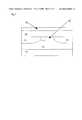
- FIG. 1is perspective view of an optical device according to one embodiment of the invention.
- FIGS. 2 - 4are views of the device of FIG. 1 during various stages of fabrication.
- FIG. 5is a front view of a device according to a further embodiment of the invention.
- FIG. 1illustrates a typical electroabsorption modulated laser (EML) device, 10 , which includes features of the invention.
- the device, 10basically comprises two portions, a laser portion, 11 , and a modulator portion, 12 , formed on a single substrate. 13 .
- the substrate, 13typically comprises InP.
- Formed on the substrate. 13is a waveguide region. 14 , which comprises a combination of active layer and optical confinement layer and is typically InGaAsP.
- the region, 14includes a p-n junction, 26 .
- the properties of the constituents of the waveguide 14are chosen so that in the laser portion, 11 , the waveguide will function as an active region and in the modulator portion, 12 , the waveguide will absorb a certain amount of the emitted light depending upon the electrical bias supplied thereto.
- Johnson et al“High Speed Integrated Electroabsorption Modulators”, Proceedings of SPIE, Vol. 3038, pp. 30-38 (Feb. 1997).
- a “waveguide” regionrefers to a region which will confine light to a designated portion of the device, and can include, alone or in combination, an active region, a modulator region, and a detector region (not shown).
- a blocking layer, 25is formed adjacent to the waveguide 14 .
- This layertypically comprises alternate n, p-type and intrinsic layers of InP, and is used to block current in areas outside the waveguide 14 .
- a cladding layer, 15is also formed adjacent to the waveguide, 14 , and extending above it.
- the layer, 15in combination with 14 , provides the necessary structure for proper operation of an optical waveguide.
- the layer, 15is typically a binary material, e.g., InP.
- the cladding layertypically includes Zn as a p-type dopant in a controlled profile.
- a contact layer, 16is formed over the waveguide and cladding region. This layer is doped to provide sufficient conductivity to make low resistance contact to the section, 14 .
- the layer, 16typically comprises InGaAs and includes a p-type dopant to adjust the conductivity.
- the impurityis carbon, and the impurity concentration is within the range 1 ⁇ 10 18 -5 ⁇ 10 19 cm ⁇ 3 .
- Carbonbehaves as a p-type dopant in ternary material, although it acts as n-type dopant in other material such as InP.
- the elimination of Zn dopant in the contact layer, 16effectively eliminates the problems associated with Zn migration during growth and processing, such as an increase in internal loss in the waveguide. 14 , in the laser portion. In addition, it aids in preserving the location of p-n junction. 26 , within section 14 .
- the device, 10also includes electrodes 17 and 18 formed on the contact layer. 16 , in the laser and modulator portions, 11 and 12 , respectively and an electrode, 19 , formed on the bottom surface of the substrate, 13 . These electrodes provide the bias to produce light emission in the laser portion, 11 , and control the absorption of the emitted light in the modulator portion, 12 .
- FIGS. 2 - 4A method for fabricating the device of FIG. I is illustrated in FIGS. 2 - 4 .
- the region, 14is formed on the substrate, 13 , by first forming mask segments, 20 and 21 , which are typically SiO 2 and leaving a central portion of the substrate exposed.
- the region 14is then grown on the exposed surface typically by metallorganic chemical vapor deposition (MOCVD) or gas source molecular beam epitaxy (GSMBE).
- MOCVDmetalorganic chemical vapor deposition
- GSMBEgas source molecular beam epitaxy
- segments 20 and 21are then removed, another SiO 2 mask (not shown) is formed on the region, 14 , and then the region is etched to form a mesa structure.
- the blocking layer 25 and cladding layer, 15are then formed by epitaxially growing the semiconductor layers on the exposed surfaces of the substrate, 13 . This is usually done by MOCVD.
- the layer, 15typically includes a Zn dopant having a desired profile as a function of the layer thickness so as to form the p-n junction.
- the concentration of Zn dopantusually varies from 5 ⁇ 10 17 cm 3 to 3 ⁇ 10 18 cm 3 .
- the contact layer, 16is formed on the cladding layer, 15 , typically by MOCVD.
- the layer, 16includes carbon as a p-type dopant to provide the desired conductivity.
- the dopant concentrationis in the range 2 ⁇ 10 18 -3 ⁇ 10 19 cm ⁇ 3 .
- the contact layer. 16is typically InGaAs, but other materials such as InGaAsP might be employed if carbon will act as a p-type dopant therein.
- the layer 16is typically 0.1 ⁇ m-0.5 ⁇ m micron thick.
- Electrodes 17 , 18 and 19are typically Ti/Pt/Au or Be-Au and deposited by e-beam evaporation.
- a capped Mesa Buried Heterostructure (CMBH) laserillustrated in FIG. 5, includes a substrate, 30 , typically InP on which is formed a n-type undercladding layer 31 , an active region and waveguide, 32 , for light emission, and blocking regions, 33 and 34 , adjacent to the active region, layer 35 .
- the active regiontypically comprises MQW or bulk layers of InGaAsP, and the blocking regions, 33 and 34 , typically comprise InP.
- a p-type cladding layer, 35comprising typically InP was formed over the waveguide and active region. This was followed by the growth of layer 36 as a contact layer.
- the contact layer, 36was InGaAs and include carbon as the p-type dopant with a concentration in the range 1 ⁇ 10 18 -3 ⁇ 10 19 cm ⁇ 3 .
Landscapes
- Physics & Mathematics (AREA)
- Condensed Matter Physics & Semiconductors (AREA)
- General Physics & Mathematics (AREA)
- Electromagnetism (AREA)
- Optics & Photonics (AREA)
- Semiconductor Lasers (AREA)
Abstract
Description
- This invention relates to semiconductor optical devices, including lasers and electroabsorption modulators, and detectors.[0001]
- Electroabsorption modulated laser (EML) devices have recently received a great deal of attention for use in high speed optical systems. Such devices typically include a semiconductor laser and modulator found in a single substrate. These devices usually include a semiconductor multi quantum well (MQW) active region, a contact layer formed thereover to facilitate electrical contact with the active layer, a current blocking layer for directing current to the active region, and a cladding layer to continue light to the active region. Zn is a commonly used p-type dopant for the blocking, contact and cladding layers, and the performance of the laser and modulator depends critically on the level of Zn in the various layers of the device.[0002]
- It is desired to maintain a certain Zn dopant profile in the device structure for optimum performance. However, the Zn profile in the blocking and cladding layers may get modified during the growth of the contact layer due to the migration of the Zn dopant from the contact layer. One solution to the problem is to reduce the amount of Zn in the cladding, blocking, and contact layers. However, this approach also adversely affects other device properties, such as total device resistance.[0003]
- It is desirable, therefore, to provide a process and resulting device which mitigate the problem of Zn migration in optical devices.[0004]
- The invention in accordance with one aspect is an optical device comprising a semiconductor waveguide region (which may include an active region), a cladding region including a dopant comprising in, formed adjacent to the waveguide region, and a semiconductor contact region. The contact region is selected from the materials InGaAs and InGaAsP, and is formed over the waveguide region. The contact region includes a p-type dopant comprising carbon to provide sufficient conductivity to make low resistance contact to the waveguide region.[0005]
- In accordance with another aspect the invention is a method of fabricating an optical device including the steps of epitaxially forming a semiconductor waveguide region over the substrate, and forming a cladding region adjacent to the waveguide region, the cladding region including a dopant comprising Zn. A contact region selected from the materials InGaAs and InGaAsP is epitaxially formed over the waveguide region. The contact layer includes a p-type dopant comprising carbon to provide sufficient conductivity to make a low resistance contact to the waveguide region.[0006]
- These and other features of the invention are delineated in detail in the following description. In the drawing:[0007]
- FIG. 1 is perspective view of an optical device according to one embodiment of the invention.[0008]
- FIGS.[0009]2-4 are views of the device of FIG. 1 during various stages of fabrication; and
- FIG. 5 is a front view of a device according to a further embodiment of the invention.[0010]
- It will be appreciated that, for purposes of illustration, these figures are not necessarily drawn to scale.[0011]
- FIG. 1 illustrates a typical electroabsorption modulated laser (EML) device,[0012]10, which includes features of the invention. The device,10, basically comprises two portions, a laser portion,11, and a modulator portion,12, formed on a single substrate.13. The substrate,13, typically comprises InP. Formed on the substrate.13, is a waveguide region.14, which comprises a combination of active layer and optical confinement layer and is typically InGaAsP. The region,14, includes a p-n junction,26. As known in the art, the properties of the constituents of the
waveguide 14 are chosen so that in the laser portion,11, the waveguide will function as an active region and in the modulator portion,12, the waveguide will absorb a certain amount of the emitted light depending upon the electrical bias supplied thereto. (See, e.g., Johnson et al “High Speed Integrated Electroabsorption Modulators”, Proceedings of SPIE, Vol. 3038, pp. 30-38 (Feb. 1997). - Thus, in the context of this application, a “waveguide” region refers to a region which will confine light to a designated portion of the device, and can include, alone or in combination, an active region, a modulator region, and a detector region (not shown).[0013]
- A blocking layer,[0014]25, is formed adjacent to the
waveguide 14. This layer typically comprises alternate n, p-type and intrinsic layers of InP, and is used to block current in areas outside thewaveguide 14. - A cladding layer,[0015]15, is also formed adjacent to the waveguide,14, and extending above it. The layer,15, in combination with14, provides the necessary structure for proper operation of an optical waveguide. The layer,15, is typically a binary material, e.g., InP. The cladding layer typically includes Zn as a p-type dopant in a controlled profile. A contact layer,16, is formed over the waveguide and cladding region. This layer is doped to provide sufficient conductivity to make low resistance contact to the section,14. The layer,16, typically comprises InGaAs and includes a p-type dopant to adjust the conductivity. In accordance with a preferred embodiment, the impurity is carbon, and the impurity concentration is within the range 1×10¹⁸-5×1019cm−3. Carbon behaves as a p-type dopant in ternary material, although it acts as n-type dopant in other material such as InP. The elimination of Zn dopant in the contact layer,16, effectively eliminates the problems associated with Zn migration during growth and processing, such as an increase in internal loss in the waveguide.14, in the laser portion. In addition, it aids in preserving the location of p-n junction.26, within
section 14. - The device,[0016]10, also includes
electrodes - A method for fabricating the device of FIG. I is illustrated in FIGS.[0017]2-4. As illustrated in FIG. 2, the region,14, is formed on the substrate,13, by first forming mask segments,20 and21, which are typically SiO2and leaving a central portion of the substrate exposed. The
region 14 is then grown on the exposed surface typically by metallorganic chemical vapor deposition (MOCVD) or gas source molecular beam epitaxy (GSMBE). - Typically,[0018]
segments - As illustrated in FIG. 3, the[0019]
blocking layer 25 and cladding layer,15, are then formed by epitaxially growing the semiconductor layers on the exposed surfaces of the substrate,13. This is usually done by MOCVD. The layer,15, typically includes a Zn dopant having a desired profile as a function of the layer thickness so as to form the p-n junction. For example, the concentration of Zn dopant usually varies from 5×1017cm3to 3×1018cm3. - As illustrated in FIG. 4, the contact layer,[0020]16, is formed on the cladding layer,15, typically by MOCVD. The layer,16, includes carbon as a p-type dopant to provide the desired conductivity. Preferably, the dopant concentration is in the range 2×10¹⁸-3×1019cm−3. The contact layer.16, is typically InGaAs, but other materials such as InGaAsP might be employed if carbon will act as a p-type dopant therein. The
layer 16, is typically 0.1 μm-0.5 μm micron thick. - The structure is completed by depositing[0021]
electrodes - While the invention has been described with reference to an EML device, it should be apparent that it is useful for other optical devices requiring a p-type contact layer. For example, a capped Mesa Buried Heterostructure (CMBH) laser, illustrated in FIG. 5, includes a substrate,[0022]30, typically InP on which is formed a n-
type undercladding layer 31, an active region and waveguide,32, for light emission, and blocking regions,33 and34, adjacent to the active region,layer 35. The active region typically comprises MQW or bulk layers of InGaAsP, and the blocking regions,33 and34, typically comprise InP. A p-type cladding layer,35, comprising typically InP was formed over the waveguide and active region. This was followed by the growth oflayer 36 as a contact layer. The contact layer,36, was InGaAs and include carbon as the p-type dopant with a concentration in the range 1×10¹⁸-3×1019cm−3. - This device was tested, and it was discovered that such lasers have lower threshold currents and higher slope efficiency than similar devices made with Zn-doped contact layers. Further, the internal loss in the laser cavity was lower for devices made in accordance with the invention as a result of the absence of Zn diffusion into the active region.[0023]
Claims (7)
Applications Claiming Priority (1)
| Application Number | Priority Date | Filing Date | Title |
|---|---|---|---|
| US09/097,205US6317444B1 (en) | 1998-06-12 | 1998-06-12 | Optical device including carbon-doped contact layers |
Publications (1)
| Publication Number | Publication Date |
|---|---|
| US20010040907A1true US20010040907A1 (en) | 2001-11-15 |
Family
ID=22262037
Family Applications (2)
| Application Number | Title | Priority Date | Filing Date |
|---|---|---|---|
| US09/097,205GrantedUS20010040907A1 (en) | 1998-06-12 | 1998-06-12 | Optical device including carbon-doped contact layers |
| US09/097,205Expired - LifetimeUS6317444B1 (en) | 1998-06-12 | 1998-06-12 | Optical device including carbon-doped contact layers |
Family Applications After (1)
| Application Number | Title | Priority Date | Filing Date |
|---|---|---|---|
| US09/097,205Expired - LifetimeUS6317444B1 (en) | 1998-06-12 | 1998-06-12 | Optical device including carbon-doped contact layers |
Country Status (4)
| Country | Link |
|---|---|
| US (2) | US20010040907A1 (en) |
| EP (1) | EP0964489A1 (en) |
| JP (1) | JP2000031580A (en) |
| CN (1) | CN1239342A (en) |
Cited By (26)
| Publication number | Priority date | Publication date | Assignee | Title |
|---|---|---|---|---|
| US7479421B2 (en) | 2005-09-28 | 2009-01-20 | Intel Corporation | Process for integrating planar and non-planar CMOS transistors on a bulk substrate and article made thereby |
| US7518196B2 (en)* | 2005-02-23 | 2009-04-14 | Intel Corporation | Field effect transistor with narrow bandgap source and drain regions and method of fabrication |
| US7547637B2 (en) | 2005-06-21 | 2009-06-16 | Intel Corporation | Methods for patterning a semiconductor film |
| US7550333B2 (en) | 2004-10-25 | 2009-06-23 | Intel Corporation | Nonplanar device with thinned lower body portion and method of fabrication |
| US7579280B2 (en) | 2004-06-01 | 2009-08-25 | Intel Corporation | Method of patterning a film |
| US7736956B2 (en) | 2005-08-17 | 2010-06-15 | Intel Corporation | Lateral undercut of metal gate in SOI device |
| US7781771B2 (en) | 2004-03-31 | 2010-08-24 | Intel Corporation | Bulk non-planar transistor having strained enhanced mobility and methods of fabrication |
| US7820513B2 (en) | 2003-06-27 | 2010-10-26 | Intel Corporation | Nonplanar semiconductor device with partially or fully wrapped around gate electrode and methods of fabrication |
| US7879675B2 (en) | 2005-03-14 | 2011-02-01 | Intel Corporation | Field effect transistor with metal source/drain regions |
| US7898041B2 (en) | 2005-06-30 | 2011-03-01 | Intel Corporation | Block contact architectures for nanoscale channel transistors |
| US7902014B2 (en) | 2005-09-28 | 2011-03-08 | Intel Corporation | CMOS devices with a single work function gate electrode and method of fabrication |
| US7960794B2 (en) | 2004-08-10 | 2011-06-14 | Intel Corporation | Non-planar pMOS structure with a strained channel region and an integrated strained CMOS flow |
| US7989280B2 (en) | 2005-11-30 | 2011-08-02 | Intel Corporation | Dielectric interface for group III-V semiconductor device |
| US8084818B2 (en) | 2004-06-30 | 2011-12-27 | Intel Corporation | High mobility tri-gate devices and methods of fabrication |
| US8268709B2 (en) | 2004-09-29 | 2012-09-18 | Intel Corporation | Independently accessed double-gate and tri-gate transistors in same process flow |
| US8362566B2 (en) | 2008-06-23 | 2013-01-29 | Intel Corporation | Stress in trigate devices using complimentary gate fill materials |
| US8405164B2 (en) | 2003-06-27 | 2013-03-26 | Intel Corporation | Tri-gate transistor device with stress incorporation layer and method of fabrication |
| US8617945B2 (en) | 2006-08-02 | 2013-12-31 | Intel Corporation | Stacking fault and twin blocking barrier for integrating III-V on Si |
| US9337307B2 (en) | 2005-06-15 | 2016-05-10 | Intel Corporation | Method for fabricating transistor with thinned channel |
| CN106461987A (en)* | 2014-02-24 | 2017-02-22 | 洛克利光子有限公司 | Detector remodulator |
| US10401656B2 (en) | 2017-07-05 | 2019-09-03 | Rockley Photonics Limited | Optoelectronic device |
| US10928659B2 (en) | 2014-02-24 | 2021-02-23 | Rockley Photonics Limited | Optoelectronic device |
| US11036006B2 (en) | 2016-12-02 | 2021-06-15 | Rockley Photonics Limited | Waveguide device and method of doping a waveguide device |
| US11101256B2 (en) | 2016-11-23 | 2021-08-24 | Rockley Photonics Limited | Optical modulators |
| US11105975B2 (en) | 2016-12-02 | 2021-08-31 | Rockley Photonics Limited | Waveguide optoelectronic device |
| US11150494B2 (en) | 2015-03-05 | 2021-10-19 | Rockley Photonics Limited | Waveguide modulator structures |
Families Citing this family (9)
| Publication number | Priority date | Publication date | Assignee | Title |
|---|---|---|---|---|
| US7160746B2 (en) | 2001-07-27 | 2007-01-09 | Lightwave Microsystems Corporation | GeBPSG top clad for a planar lightwave circuit |
| US6553170B2 (en) | 2001-08-31 | 2003-04-22 | Lightwave Microsystems Corporation | Method and system for a combination of high boron and low boron BPSG top clad fabrication process for a planar lightwave circuit |
| JP4500516B2 (en)* | 2002-12-13 | 2010-07-14 | 三菱電機株式会社 | Semiconductor laser device and manufacturing method thereof |
| US7142342B2 (en)* | 2003-06-02 | 2006-11-28 | Avago Technologies Fiber Ip (Singapore) Pte. Ltd. | Electroabsorption modulator |
| DE102004006648B4 (en)* | 2004-02-11 | 2008-11-13 | Pfw Aerospace Ag | Cargo hold floor for aircraft |
| US7332439B2 (en) | 2004-09-29 | 2008-02-19 | Intel Corporation | Metal gate transistors with epitaxial source and drain regions |
| JP5243901B2 (en)* | 2008-09-19 | 2013-07-24 | 日本オクラロ株式会社 | Coaxial type semiconductor optical module |
| CN111682400B (en)* | 2020-06-22 | 2021-07-20 | 苏州长光华芯光电技术股份有限公司 | Method for manufacturing contact layer, semiconductor laser and manufacturing method thereof |
| EP4568030A1 (en)* | 2022-08-04 | 2025-06-11 | Sumitomo Electric Industries, Ltd. | Semiconductor laminate, semiconductor element, and method for producing semiconductor laminate |
Family Cites Families (9)
| Publication number | Priority date | Publication date | Assignee | Title |
|---|---|---|---|---|
| JPS61258487A (en) | 1985-05-11 | 1986-11-15 | Fujitsu Ltd | Manufacturing method of quantum well laser |
| JPH01214190A (en) | 1988-02-23 | 1989-08-28 | Toshiba Corp | Semiconductor laser device |
| JPH05198895A (en) | 1991-10-31 | 1993-08-06 | Fujitsu Ltd | Semiconductor light emitting device and method of manufacturing the same |
| US5212703A (en)* | 1992-02-18 | 1993-05-18 | Eastman Kodak Company | Surface emitting lasers with low resistance bragg reflectors |
| JP2809124B2 (en) | 1995-02-09 | 1998-10-08 | 日本電気株式会社 | Optical semiconductor integrated device and method of manufacturing the same |
| US5706306A (en)* | 1996-03-15 | 1998-01-06 | Motorola | VCSEL with distributed Bragg reflectors for visible light |
| US5719893A (en) | 1996-07-17 | 1998-02-17 | Motorola, Inc. | Passivated vertical cavity surface emitting laser |
| US5818861A (en)* | 1996-07-19 | 1998-10-06 | Hewlett-Packard Company | Vertical cavity surface emitting laser with low band gap highly doped contact layer |
| JPH10135567A (en) | 1996-11-01 | 1998-05-22 | Sharp Corp | Semiconductor laser device |
- 1998
- 1998-06-12USUS09/097,205patent/US20010040907A1/enactiveGranted
- 1998-06-12USUS09/097,205patent/US6317444B1/ennot_activeExpired - Lifetime
- 1999
- 1999-06-08EPEP99304469Apatent/EP0964489A1/ennot_activeWithdrawn
- 1999-06-11CNCN99108378Apatent/CN1239342A/enactivePending
- 1999-06-11JPJP11165298Apatent/JP2000031580A/enactivePending
Cited By (61)
| Publication number | Priority date | Publication date | Assignee | Title |
|---|---|---|---|---|
| US20110020987A1 (en)* | 2003-06-27 | 2011-01-27 | Hareland Scott A | Nonplanar semiconductor device with partially or fully wrapped around gate electrode and methods of fabrication |
| US8273626B2 (en) | 2003-06-27 | 2012-09-25 | Intel Corporationn | Nonplanar semiconductor device with partially or fully wrapped around gate electrode and methods of fabrication |
| US8405164B2 (en) | 2003-06-27 | 2013-03-26 | Intel Corporation | Tri-gate transistor device with stress incorporation layer and method of fabrication |
| US7820513B2 (en) | 2003-06-27 | 2010-10-26 | Intel Corporation | Nonplanar semiconductor device with partially or fully wrapped around gate electrode and methods of fabrication |
| US7781771B2 (en) | 2004-03-31 | 2010-08-24 | Intel Corporation | Bulk non-planar transistor having strained enhanced mobility and methods of fabrication |
| US7579280B2 (en) | 2004-06-01 | 2009-08-25 | Intel Corporation | Method of patterning a film |
| US8084818B2 (en) | 2004-06-30 | 2011-12-27 | Intel Corporation | High mobility tri-gate devices and methods of fabrication |
| US7960794B2 (en) | 2004-08-10 | 2011-06-14 | Intel Corporation | Non-planar pMOS structure with a strained channel region and an integrated strained CMOS flow |
| US8399922B2 (en) | 2004-09-29 | 2013-03-19 | Intel Corporation | Independently accessed double-gate and tri-gate transistors |
| US8268709B2 (en) | 2004-09-29 | 2012-09-18 | Intel Corporation | Independently accessed double-gate and tri-gate transistors in same process flow |
| US8749026B2 (en) | 2004-10-25 | 2014-06-10 | Intel Corporation | Nonplanar device with thinned lower body portion and method of fabrication |
| US8502351B2 (en) | 2004-10-25 | 2013-08-06 | Intel Corporation | Nonplanar device with thinned lower body portion and method of fabrication |
| US9190518B2 (en) | 2004-10-25 | 2015-11-17 | Intel Corporation | Nonplanar device with thinned lower body portion and method of fabrication |
| US7550333B2 (en) | 2004-10-25 | 2009-06-23 | Intel Corporation | Nonplanar device with thinned lower body portion and method of fabrication |
| US9741809B2 (en) | 2004-10-25 | 2017-08-22 | Intel Corporation | Nonplanar device with thinned lower body portion and method of fabrication |
| US10236356B2 (en) | 2004-10-25 | 2019-03-19 | Intel Corporation | Nonplanar device with thinned lower body portion and method of fabrication |
| US8067818B2 (en) | 2004-10-25 | 2011-11-29 | Intel Corporation | Nonplanar device with thinned lower body portion and method of fabrication |
| US9614083B2 (en)* | 2005-02-23 | 2017-04-04 | Intel Corporation | Field effect transistor with narrow bandgap source and drain regions and method of fabrication |
| US8664694B2 (en) | 2005-02-23 | 2014-03-04 | Intel Corporation | Field effect transistor with narrow bandgap source and drain regions and method of fabrication |
| US8183646B2 (en)* | 2005-02-23 | 2012-05-22 | Intel Corporation | Field effect transistor with narrow bandgap source and drain regions and method of fabrication |
| US7518196B2 (en)* | 2005-02-23 | 2009-04-14 | Intel Corporation | Field effect transistor with narrow bandgap source and drain regions and method of fabrication |
| US10121897B2 (en) | 2005-02-23 | 2018-11-06 | Intel Corporation | Field effect transistor with narrow bandgap source and drain regions and method of fabrication |
| US9748391B2 (en) | 2005-02-23 | 2017-08-29 | Intel Corporation | Field effect transistor with narrow bandgap source and drain regions and method of fabrication |
| US9368583B2 (en) | 2005-02-23 | 2016-06-14 | Intel Corporation | Field effect transistor with narrow bandgap source and drain regions and method of fabrication |
| US9048314B2 (en) | 2005-02-23 | 2015-06-02 | Intel Corporation | Field effect transistor with narrow bandgap source and drain regions and method of fabrication |
| US8368135B2 (en) | 2005-02-23 | 2013-02-05 | Intel Corporation | Field effect transistor with narrow bandgap source and drain regions and method of fabrication |
| US8816394B2 (en) | 2005-02-23 | 2014-08-26 | Intel Corporation | Field effect transistor with narrow bandgap source and drain regions and method of fabrication |
| US7893506B2 (en) | 2005-02-23 | 2011-02-22 | Intel Corporation | Field effect transistor with narrow bandgap source and drain regions and method of fabrication |
| US7825481B2 (en) | 2005-02-23 | 2010-11-02 | Intel Corporation | Field effect transistor with narrow bandgap source and drain regions and method of fabrication |
| US7879675B2 (en) | 2005-03-14 | 2011-02-01 | Intel Corporation | Field effect transistor with metal source/drain regions |
| US9806195B2 (en) | 2005-06-15 | 2017-10-31 | Intel Corporation | Method for fabricating transistor with thinned channel |
| US9337307B2 (en) | 2005-06-15 | 2016-05-10 | Intel Corporation | Method for fabricating transistor with thinned channel |
| US11978799B2 (en) | 2005-06-15 | 2024-05-07 | Tahoe Research, Ltd. | Method for fabricating transistor with thinned channel |
| US10937907B2 (en) | 2005-06-15 | 2021-03-02 | Intel Corporation | Method for fabricating transistor with thinned channel |
| US10367093B2 (en) | 2005-06-15 | 2019-07-30 | Intel Corporation | Method for fabricating transistor with thinned channel |
| US7547637B2 (en) | 2005-06-21 | 2009-06-16 | Intel Corporation | Methods for patterning a semiconductor film |
| US9385180B2 (en) | 2005-06-21 | 2016-07-05 | Intel Corporation | Semiconductor device structures and methods of forming semiconductor structures |
| US8071983B2 (en) | 2005-06-21 | 2011-12-06 | Intel Corporation | Semiconductor device structures and methods of forming semiconductor structures |
| US8581258B2 (en) | 2005-06-21 | 2013-11-12 | Intel Corporation | Semiconductor device structures and methods of forming semiconductor structures |
| US8933458B2 (en) | 2005-06-21 | 2015-01-13 | Intel Corporation | Semiconductor device structures and methods of forming semiconductor structures |
| US9761724B2 (en) | 2005-06-21 | 2017-09-12 | Intel Corporation | Semiconductor device structures and methods of forming semiconductor structures |
| US7898041B2 (en) | 2005-06-30 | 2011-03-01 | Intel Corporation | Block contact architectures for nanoscale channel transistors |
| US7736956B2 (en) | 2005-08-17 | 2010-06-15 | Intel Corporation | Lateral undercut of metal gate in SOI device |
| US8193567B2 (en) | 2005-09-28 | 2012-06-05 | Intel Corporation | Process for integrating planar and non-planar CMOS transistors on a bulk substrate and article made thereby |
| US7479421B2 (en) | 2005-09-28 | 2009-01-20 | Intel Corporation | Process for integrating planar and non-planar CMOS transistors on a bulk substrate and article made thereby |
| US7902014B2 (en) | 2005-09-28 | 2011-03-08 | Intel Corporation | CMOS devices with a single work function gate electrode and method of fabrication |
| US8294180B2 (en) | 2005-09-28 | 2012-10-23 | Intel Corporation | CMOS devices with a single work function gate electrode and method of fabrication |
| US7989280B2 (en) | 2005-11-30 | 2011-08-02 | Intel Corporation | Dielectric interface for group III-V semiconductor device |
| US8617945B2 (en) | 2006-08-02 | 2013-12-31 | Intel Corporation | Stacking fault and twin blocking barrier for integrating III-V on Si |
| US9450092B2 (en) | 2008-06-23 | 2016-09-20 | Intel Corporation | Stress in trigate devices using complimentary gate fill materials |
| US9806193B2 (en) | 2008-06-23 | 2017-10-31 | Intel Corporation | Stress in trigate devices using complimentary gate fill materials |
| US8362566B2 (en) | 2008-06-23 | 2013-01-29 | Intel Corporation | Stress in trigate devices using complimentary gate fill materials |
| US9224754B2 (en) | 2008-06-23 | 2015-12-29 | Intel Corporation | Stress in trigate devices using complimentary gate fill materials |
| US8741733B2 (en) | 2008-06-23 | 2014-06-03 | Intel Corporation | Stress in trigate devices using complimentary gate fill materials |
| CN106461987A (en)* | 2014-02-24 | 2017-02-22 | 洛克利光子有限公司 | Detector remodulator |
| US10928659B2 (en) | 2014-02-24 | 2021-02-23 | Rockley Photonics Limited | Optoelectronic device |
| US11150494B2 (en) | 2015-03-05 | 2021-10-19 | Rockley Photonics Limited | Waveguide modulator structures |
| US11101256B2 (en) | 2016-11-23 | 2021-08-24 | Rockley Photonics Limited | Optical modulators |
| US11036006B2 (en) | 2016-12-02 | 2021-06-15 | Rockley Photonics Limited | Waveguide device and method of doping a waveguide device |
| US11105975B2 (en) | 2016-12-02 | 2021-08-31 | Rockley Photonics Limited | Waveguide optoelectronic device |
| US10401656B2 (en) | 2017-07-05 | 2019-09-03 | Rockley Photonics Limited | Optoelectronic device |
Also Published As
| Publication number | Publication date |
|---|---|
| EP0964489A1 (en) | 1999-12-15 |
| CN1239342A (en) | 1999-12-22 |
| JP2000031580A (en) | 2000-01-28 |
| US6317444B1 (en) | 2001-11-13 |
Similar Documents
| Publication | Publication Date | Title |
|---|---|---|
| US6317444B1 (en) | Optical device including carbon-doped contact layers | |
| US6437372B1 (en) | Diffusion barrier spikes for III-V structures | |
| US4864581A (en) | Semiconductor structures and a method of manufacturing semiconductor structures | |
| EP0132081B1 (en) | Semiconductor laser device | |
| EP0103415A2 (en) | Light-emitting semiconductor devices and methods of producing the same | |
| US6911713B2 (en) | Optical device having a carrier-depleted layer | |
| US5661743A (en) | Semiconductor laser | |
| US5020068A (en) | Semiconductor laser device | |
| EP0083697A1 (en) | Double channel planar buried heterostructure laser | |
| US6391671B2 (en) | Method of producing an optical semiconductor device having a waveguide layer buried in an InP current blocking layer | |
| US6706542B1 (en) | Application of InAIAs double-layer to block dopant out-diffusion in III-V device Fabrication | |
| US4766472A (en) | Monolithic semiconductor structure of a laser and a field effect transistor | |
| US5335241A (en) | Buried stripe type semiconductor laser device | |
| EP0293000B1 (en) | Light emitting device | |
| US5309465A (en) | Ridge waveguide semiconductor laser with thin active region | |
| EP0915542B1 (en) | Semiconductor laser having improved current blocking layers and method of forming the same | |
| US6819695B1 (en) | Dopant diffusion barrier layer for use in III-V structures | |
| US5770471A (en) | Method of making semiconductor laser with aluminum-free etch stopping layer | |
| US5518954A (en) | Method for fabricating a semiconductor laser | |
| JPH09214045A (en) | Semiconductor laser and manufacturing method thereof | |
| EP1271722A1 (en) | Semiconductor laser structure and method of manufacturing same | |
| US5572539A (en) | II-VI semiconductor laser with different guide layers | |
| US20030112841A1 (en) | Means of controlling dopant diffusion in a semiconductor heterostructure | |
| US4517674A (en) | Zinc-diffused narrow stripe AlGaAs/GaAs double heterostructure laser | |
| US20030062517A1 (en) | Semiconductor device with current confinement structure |
Legal Events
| Date | Code | Title | Description |
|---|---|---|---|
| AS | Assignment | Owner name:DEUTSCHE BANK AG NEW YORK BRANCH, AS COLLATERAL AG Free format text:PATENT SECURITY AGREEMENT;ASSIGNORS:LSI CORPORATION;AGERE SYSTEMS LLC;REEL/FRAME:032856/0031 Effective date:20140506 | |
| AS | Assignment | Owner name:AVAGO TECHNOLOGIES GENERAL IP (SINGAPORE) PTE. LTD Free format text:ASSIGNMENT OF ASSIGNORS INTEREST;ASSIGNOR:AGERE SYSTEMS LLC;REEL/FRAME:035365/0634 Effective date:20140804 | |
| AS | Assignment | Owner name:LSI CORPORATION, CALIFORNIA Free format text:TERMINATION AND RELEASE OF SECURITY INTEREST IN PATENT RIGHTS (RELEASES RF 032856-0031);ASSIGNOR:DEUTSCHE BANK AG NEW YORK BRANCH, AS COLLATERAL AGENT;REEL/FRAME:037684/0039 Effective date:20160201 Owner name:AGERE SYSTEMS LLC, PENNSYLVANIA Free format text:TERMINATION AND RELEASE OF SECURITY INTEREST IN PATENT RIGHTS (RELEASES RF 032856-0031);ASSIGNOR:DEUTSCHE BANK AG NEW YORK BRANCH, AS COLLATERAL AGENT;REEL/FRAME:037684/0039 Effective date:20160201 | |
| AS | Assignment | Owner name:BANK OF AMERICA, N.A., AS COLLATERAL AGENT, NORTH CAROLINA Free format text:PATENT SECURITY AGREEMENT;ASSIGNOR:AVAGO TECHNOLOGIES GENERAL IP (SINGAPORE) PTE. LTD.;REEL/FRAME:037808/0001 Effective date:20160201 Owner name:BANK OF AMERICA, N.A., AS COLLATERAL AGENT, NORTH Free format text:PATENT SECURITY AGREEMENT;ASSIGNOR:AVAGO TECHNOLOGIES GENERAL IP (SINGAPORE) PTE. LTD.;REEL/FRAME:037808/0001 Effective date:20160201 | |
| AS | Assignment | Owner name:AVAGO TECHNOLOGIES GENERAL IP (SINGAPORE) PTE. LTD., SINGAPORE Free format text:TERMINATION AND RELEASE OF SECURITY INTEREST IN PATENTS;ASSIGNOR:BANK OF AMERICA, N.A., AS COLLATERAL AGENT;REEL/FRAME:041710/0001 Effective date:20170119 Owner name:AVAGO TECHNOLOGIES GENERAL IP (SINGAPORE) PTE. LTD Free format text:TERMINATION AND RELEASE OF SECURITY INTEREST IN PATENTS;ASSIGNOR:BANK OF AMERICA, N.A., AS COLLATERAL AGENT;REEL/FRAME:041710/0001 Effective date:20170119 | |
| AS | Assignment | Owner name:AVAGO TECHNOLOGIES INTERNATIONAL SALES PTE. LIMITE Free format text:MERGER;ASSIGNOR:AVAGO TECHNOLOGIES GENERAL IP (SINGAPORE) PTE. LTD.;REEL/FRAME:047195/0026 Effective date:20180509 | |
| AS | Assignment | Owner name:AVAGO TECHNOLOGIES INTERNATIONAL SALES PTE. LIMITE Free format text:CORRECTIVE ASSIGNMENT TO CORRECT THE EFFECTIVE DATE OF MERGER PREVIOUSLY RECORDED ON REEL 047195 FRAME 0026. ASSIGNOR(S) HEREBY CONFIRMS THE MERGER;ASSIGNOR:AVAGO TECHNOLOGIES GENERAL IP (SINGAPORE) PTE. LTD.;REEL/FRAME:047477/0423 Effective date:20180905 |