US20010034097A1 - Method of forming metal nitride film by chemical vapor deposition and method of forming metal contact and capacitor of semiconductor device using the same - Google Patents
Method of forming metal nitride film by chemical vapor deposition and method of forming metal contact and capacitor of semiconductor device using the sameDownload PDFInfo
- Publication number
- US20010034097A1 US20010034097A1US09/765,531US76553101AUS2001034097A1US 20010034097 A1US20010034097 A1US 20010034097A1US 76553101 AUS76553101 AUS 76553101AUS 2001034097 A1US2001034097 A1US 2001034097A1
- Authority
- US
- United States
- Prior art keywords
- deposition chamber
- metal
- deposition
- source
- ticl
- Prior art date
- Legal status (The legal status is an assumption and is not a legal conclusion. Google has not performed a legal analysis and makes no representation as to the accuracy of the status listed.)
- Granted
Links
Images


Classifications
- H—ELECTRICITY
- H01—ELECTRIC ELEMENTS
- H01L—SEMICONDUCTOR DEVICES NOT COVERED BY CLASS H10
- H01L21/00—Processes or apparatus adapted for the manufacture or treatment of semiconductor or solid state devices or of parts thereof
- H01L21/70—Manufacture or treatment of devices consisting of a plurality of solid state components formed in or on a common substrate or of parts thereof; Manufacture of integrated circuit devices or of parts thereof
- H01L21/71—Manufacture of specific parts of devices defined in group H01L21/70
- H01L21/768—Applying interconnections to be used for carrying current between separate components within a device comprising conductors and dielectrics
- H01L21/76838—Applying interconnections to be used for carrying current between separate components within a device comprising conductors and dielectrics characterised by the formation and the after-treatment of the conductors
- H01L21/76841—Barrier, adhesion or liner layers
- H01L21/76843—Barrier, adhesion or liner layers formed in openings in a dielectric
- C—CHEMISTRY; METALLURGY
- C23—COATING METALLIC MATERIAL; COATING MATERIAL WITH METALLIC MATERIAL; CHEMICAL SURFACE TREATMENT; DIFFUSION TREATMENT OF METALLIC MATERIAL; COATING BY VACUUM EVAPORATION, BY SPUTTERING, BY ION IMPLANTATION OR BY CHEMICAL VAPOUR DEPOSITION, IN GENERAL; INHIBITING CORROSION OF METALLIC MATERIAL OR INCRUSTATION IN GENERAL
- C23C—COATING METALLIC MATERIAL; COATING MATERIAL WITH METALLIC MATERIAL; SURFACE TREATMENT OF METALLIC MATERIAL BY DIFFUSION INTO THE SURFACE, BY CHEMICAL CONVERSION OR SUBSTITUTION; COATING BY VACUUM EVAPORATION, BY SPUTTERING, BY ION IMPLANTATION OR BY CHEMICAL VAPOUR DEPOSITION, IN GENERAL
- C23C16/00—Chemical coating by decomposition of gaseous compounds, without leaving reaction products of surface material in the coating, i.e. chemical vapour deposition [CVD] processes
- C23C16/22—Chemical coating by decomposition of gaseous compounds, without leaving reaction products of surface material in the coating, i.e. chemical vapour deposition [CVD] processes characterised by the deposition of inorganic material, other than metallic material
- C23C16/30—Deposition of compounds, mixtures or solid solutions, e.g. borides, carbides, nitrides
- C23C16/34—Nitrides
- C—CHEMISTRY; METALLURGY
- C23—COATING METALLIC MATERIAL; COATING MATERIAL WITH METALLIC MATERIAL; CHEMICAL SURFACE TREATMENT; DIFFUSION TREATMENT OF METALLIC MATERIAL; COATING BY VACUUM EVAPORATION, BY SPUTTERING, BY ION IMPLANTATION OR BY CHEMICAL VAPOUR DEPOSITION, IN GENERAL; INHIBITING CORROSION OF METALLIC MATERIAL OR INCRUSTATION IN GENERAL
- C23C—COATING METALLIC MATERIAL; COATING MATERIAL WITH METALLIC MATERIAL; SURFACE TREATMENT OF METALLIC MATERIAL BY DIFFUSION INTO THE SURFACE, BY CHEMICAL CONVERSION OR SUBSTITUTION; COATING BY VACUUM EVAPORATION, BY SPUTTERING, BY ION IMPLANTATION OR BY CHEMICAL VAPOUR DEPOSITION, IN GENERAL
- C23C16/00—Chemical coating by decomposition of gaseous compounds, without leaving reaction products of surface material in the coating, i.e. chemical vapour deposition [CVD] processes
- C23C16/44—Chemical coating by decomposition of gaseous compounds, without leaving reaction products of surface material in the coating, i.e. chemical vapour deposition [CVD] processes characterised by the method of coating
- C23C16/455—Chemical coating by decomposition of gaseous compounds, without leaving reaction products of surface material in the coating, i.e. chemical vapour deposition [CVD] processes characterised by the method of coating characterised by the method used for introducing gases into reaction chamber or for modifying gas flows in reaction chamber
- C23C16/45523—Pulsed gas flow or change of composition over time
- C23C16/45525—Atomic layer deposition [ALD]
- C23C16/45553—Atomic layer deposition [ALD] characterized by the use of precursors specially adapted for ALD
- H—ELECTRICITY
- H01—ELECTRIC ELEMENTS
- H01L—SEMICONDUCTOR DEVICES NOT COVERED BY CLASS H10
- H01L21/00—Processes or apparatus adapted for the manufacture or treatment of semiconductor or solid state devices or of parts thereof
- H01L21/02—Manufacture or treatment of semiconductor devices or of parts thereof
- H01L21/04—Manufacture or treatment of semiconductor devices or of parts thereof the devices having potential barriers, e.g. a PN junction, depletion layer or carrier concentration layer
- H01L21/18—Manufacture or treatment of semiconductor devices or of parts thereof the devices having potential barriers, e.g. a PN junction, depletion layer or carrier concentration layer the devices having semiconductor bodies comprising elements of Group IV of the Periodic Table or AIIIBV compounds with or without impurities, e.g. doping materials
- H01L21/28—Manufacture of electrodes on semiconductor bodies using processes or apparatus not provided for in groups H01L21/20 - H01L21/268
- H01L21/283—Deposition of conductive or insulating materials for electrodes conducting electric current
- H01L21/285—Deposition of conductive or insulating materials for electrodes conducting electric current from a gas or vapour, e.g. condensation
- H01L21/28506—Deposition of conductive or insulating materials for electrodes conducting electric current from a gas or vapour, e.g. condensation of conductive layers
- H01L21/28512—Deposition of conductive or insulating materials for electrodes conducting electric current from a gas or vapour, e.g. condensation of conductive layers on semiconductor bodies comprising elements of Group IV of the Periodic Table
- H01L21/28556—Deposition of conductive or insulating materials for electrodes conducting electric current from a gas or vapour, e.g. condensation of conductive layers on semiconductor bodies comprising elements of Group IV of the Periodic Table by chemical means, e.g. CVD, LPCVD, PECVD, laser CVD
- H01L21/28562—Selective deposition
- H—ELECTRICITY
- H01—ELECTRIC ELEMENTS
- H01L—SEMICONDUCTOR DEVICES NOT COVERED BY CLASS H10
- H01L21/00—Processes or apparatus adapted for the manufacture or treatment of semiconductor or solid state devices or of parts thereof
- H01L21/70—Manufacture or treatment of devices consisting of a plurality of solid state components formed in or on a common substrate or of parts thereof; Manufacture of integrated circuit devices or of parts thereof
- H01L21/71—Manufacture of specific parts of devices defined in group H01L21/70
- H01L21/768—Applying interconnections to be used for carrying current between separate components within a device comprising conductors and dielectrics
- H01L21/76801—Applying interconnections to be used for carrying current between separate components within a device comprising conductors and dielectrics characterised by the formation and the after-treatment of the dielectrics, e.g. smoothing
- H01L21/76802—Applying interconnections to be used for carrying current between separate components within a device comprising conductors and dielectrics characterised by the formation and the after-treatment of the dielectrics, e.g. smoothing by forming openings in dielectrics
- H01L21/76804—Applying interconnections to be used for carrying current between separate components within a device comprising conductors and dielectrics characterised by the formation and the after-treatment of the dielectrics, e.g. smoothing by forming openings in dielectrics by forming tapered via holes
- H—ELECTRICITY
- H10—SEMICONDUCTOR DEVICES; ELECTRIC SOLID-STATE DEVICES NOT OTHERWISE PROVIDED FOR
- H10D—INORGANIC ELECTRIC SEMICONDUCTOR DEVICES
- H10D1/00—Resistors, capacitors or inductors
- H10D1/01—Manufacture or treatment
- H10D1/041—Manufacture or treatment of capacitors having no potential barriers
- H10D1/042—Manufacture or treatment of capacitors having no potential barriers using deposition processes to form electrode extensions
- H—ELECTRICITY
- H10—SEMICONDUCTOR DEVICES; ELECTRIC SOLID-STATE DEVICES NOT OTHERWISE PROVIDED FOR
- H10D—INORGANIC ELECTRIC SEMICONDUCTOR DEVICES
- H10D1/00—Resistors, capacitors or inductors
- H10D1/60—Capacitors
- H10D1/68—Capacitors having no potential barriers
- H10D1/692—Electrodes
- H10D1/711—Electrodes having non-planar surfaces, e.g. formed by texturisation
- H10D1/716—Electrodes having non-planar surfaces, e.g. formed by texturisation having vertical extensions
Definitions
- the present inventionrelates to a method of fabricating semiconductor devices, and more particularly, to a method of forming a metal nitride film by chemical vapor deposition (CVD) where a metal source and a nitrogen source are used as a precursor, and a method of forming a metal contact and a capacitor of a semiconductor device using the above method.
- CVDchemical vapor deposition
- a barrier metal layerwhich prevents mutual diffusion or chemical reaction between different materials, is indispensable to stabilize the contact interfaces of semiconductor devices.
- a metal nitridesuch as TiN, TaN or WN has been widely used as the barrier metal layer of semiconductor devices.
- TiNis a representative example among the above metal nitrides.
- FIGS. 9A and 9Bshow the cross-section of a via contact for connection between metal wiring.
- FIGS. 9A and 9Bshow a simple via contact and an anchor via contact, respectively.
- the formation processes thereofare as follows.
- a first metal layer composed of aluminum (Al)is formed on a semiconductor substrate 20 .
- a TiN film 40is formed as a capping film on the resultant structure by sputtering, and then an interlayer insulative film 50 or 51 is deposited.
- a contact holeis formed by etching the interlayer insulative film 50 or 51 on the first metal layer 30 .
- the step of forming an anchor A by wet etchingis added.
- Ti as an adhesive layer and TiN 60 or 61 as a barrier metal layeris deposited, a tungsten (W) plug 70 or 71 is formed to fill the contact hole, by CVD.
- tungsten at the upper portionis removed by chemical mechanical polishing or etch-back, and then a second metal layer is deposited on the resultant structure, thereby completing the connection between metal wiring.
- this last stepis not shown.
- the TiN film 60 or 61being the barrier metal layer, is deposited by sputtering, with inferior step coverage.
- the thickness of a TiN film on the bottom, comer and anchor A of the contact holeis reduced, with an increase in the aspect ratio of the via.
- Ti or Alcombines with fluorine remaining in tungsten source gas WF 6 during tungsten deposition being a subsequent process, and thus an insulative film X is formed of TiF x or ALF x , leading to a contact failure.
- a general process for forming a CVD-metal nitride filmuses a metal source containing chlorine (Cl), e.g., a precursor such as titanium chloride TiCl 4 .
- the CVD-metal nitride film using TiCl 4 as the precursorhas a high step coverage of 95% or higher and is quickly deposited, but Cl remains in the metal nitride film as impurities.
- the Cl remaining as impurities in the metal nitride filmcauses corrosion of metal wiring such as Al and increases resistivity.
- the Cl content in the metal nitride filmmust be reduced and the resistivity must be lowered, by deposition at high temperature.
- a deposition temperature of at least 675° C.is required to obtain resistivity of 200 ⁇ -cm or less.
- a deposition temperature of 600° C. or moreexceeds thermal budget and thermal stress limits which an underlayer can withstand.
- a deposition temperature of 480° C. or loweris required, so that a high temperature CVD-metal nitride film process cannot be used.
- a low temperature deposition CVD-metal nitride film processis possible, by adding MH (methylhydrazine, (CH 3 )HNNH 2 ) to the metal source such as TiCl 4 , but this method has a defect in that step coverage is decreased to 70% or lower.
- Another method capable of low temperature depositionis to form a MOCVD-metal nitride film using a metalorganic precursor such as TDEAT (tetrakis diethylamino Ti, Ti(N(CH 2 CH 3 ) 2 ) 4 ), or TDMAT (tetrakis dimethylamino Ti, Ti(N(CH 3 ) 2 ) 4 ).
- TDEATtetrakis diethylamino Ti, Ti(N(CH 2 CH 3 ) 2 ) 4
- TDMATtetrakis dimethylamino Ti, Ti(N(CH 3 ) 2 ) 4
- the MOCVD-metal nitride filmhas no problems due to Cl and can be deposited at low temperature. However, the MOCVD-metal nitride film contains a lot of carbon (C) as impurities, giving high resistivity, and has inferior step coverage of 70% or less.
- a method of forming a metal nitride film using atomic layer epitaxy (ALE)has been tried as an alternative to deposition, in order to overcome the problems due to Cl.
- ALEatomic layer epitaxy
- the ALEgrows the metal nitride film in units of an atomic layer using only chemical absorption, and the deposition speed (0.25 A/cycle or less) is too slow to apply the ALE to mass production.
- a TiN filmis also used as the electrode of a semiconductor capacitor.
- the TiN filmis usually used in a capacitor which uses tantalum oxide (Ta 2 O 5 ) as a dielectric film.
- Semiconductor capacitors, which use the TiN film as an electrode,also have the above-described problems.
- a semiconductor capacitorin order for a semiconductor capacitor to have a high capacitance per unit area of a semiconductor substrate, its electrode is designed three-dimensionally, as in cylindrical capacitors. Hence, the shape of the semiconductor capacitor is so complicated that it is critical to guarantee step coverage of deposited materials as its electrode. Accordingly, a TiN electrode formed by CVD using a Cl-containing metal source having an excellent step coverage as a precursor has been used as the electrode of a capacitor. However, as described above, the CVDed TiN film provokes corrosion of metal wiring and gives high resistivity, due to a high concentration of Cl, resulting in a degradation in the leakage current characteristics of a capacitor.
- an objective of the present inventionis to provide a method of forming a metal nitride film, which gives excellent step coverage even at a high deposition speed and a low temperature, low impurity concentration, and low resistivity.
- Another objective of the present inventionis to provide a method of forming a metal contact having a barrier metal layer which has excellent step coverage even at a high deposition speed and a low temperature, low impurity concentration, and low resistivity, by applying the metal nitride film formation method to a metal contact of a semiconductor device.
- Still another objective of the present inventionis to provide a method of forming a capacitor which gives excellent step coverage, low impurity concentration and low resistivity, using the metal nitride film formation method.
- a method of forming a metal nitride film using chemical vapor deposition (CVD) in which a metal source and a nitrogen source are used as a precursorin which a metal source and a nitrogen source are used as a precursor.
- CVDchemical vapor deposition
- a semiconductor substrateis introduced into a deposition chamber, and the metal source flows into the deposition chamber.
- a purge gasis introduced into the deposition chamber.
- the purge gasis cut off and the nitrogen source gas flows into the deposition chamber to react with the metal source adsorbed on the semiconductor substrate.
- the nitrogen source gas remaining in the deposition chamberis removed by cutting off the inflow of the nitrogen source gas and flowing the purge gas into the deposition chamber.
- the metal nitride filmis formed on the semiconductor substrate.
- a gas inflow cycle of a sequence of the metal source, the purge gas, the nitrogen source, and the purge gascan be repeated until a metal nitride film having a desired thickness is obtained.
- a titanium nitride film TiNcan be formed by using TiCl 4 (titanium chloride), TiCl 3 (titanium chloride), TiI 4 (titanium iodide), TiBr 2 (titanium bromide), TiF 4 (titanium fluoride), (C 5 H 5 ) 2 TiCl 2 (bis(cyclopentadienyl)titanium dichloride), ((CH 3 ) 5 C 5 ) 2 TiCl 2 (bis(pentamethylcyclopentadienyl) titanium dichloride), C 5 H 5 TiCl 3 (cyclopentadienyltitanium trichloride), C 9 H 10 BCl 3 N 6 Ti (hydrotris (1-pyrazolylborato) trichloro titanium), C 9 H 7 TiCl 3 (indenyltitanium trichloride), (C 5 (CH 3 ) 5 )TiCl 3 (pent
- the tantalum nitride film TaNcan be formed using a material selected from the group consisting of TaBr 5 (tantalum bromide), TaCl 5 (tantalum chloride), TaF 5 (tantalum fluoride), TaI 5 (Tantalum iodide), and(C 5 (CH 3 ) 5 )TaCl 4 (pentamethylcyclopentadienyltantalum tetrachloride), as the metal source, and using NH 3 as the nitrogen source.
- TaBr 5tantalum bromide
- TaCl 5tantalum chloride
- TaF 5tantalum fluoride
- TaI 5Talum iodide
- C 5 (CH 3 ) 5 )TaCl 4penentamethylcyclopentadienyltantalum tetrachloride
- the purge gasis an inert gas such as Ar or N 2 .
- 1-5 sccm of the metal sourceflows into the deposition chamber for 1 to 10 seconds
- 5-200 sccm of the nitrogen sourceflows thereinto for 1 to 10 seconds
- 10-200 sccm of the purge gasflows thereinto for 1 to 10 seconds.
- an atmospheric gassuch as Ar, He and N 2 can be continuously flowed into the deposition chamber, to maintain a constant pressure in the deposition chamber.
- the pressure in the deposition chamberis maintained to be 0.1-10 torr and the deposition temperature to be between 250° C. and 400° C.
- the pressure in the deposition chamberis maintained to be 1 to 20 torr and the deposition temperature is maintained to be between 400° C. and 500° C.
- a method of forming a metal contact of a semiconductor devicewherein a first metal layer, an interlayer insulative film, a contact hole, a barrier metal layer, a metal plug, and a second metal layer are sequentially formed on a semiconductor substrate.
- a process for forming the barrier metal layeris as follows. A metal source flows into the semiconductor substrate having the interlayer insulative film in which the contact hole exposing the first metal layer is formed. The metal source is adsorbed to the resultant structure. After a while, the metal source remaining in the deposition chamber is removed by cutting off the inflow of the metal source and flowing a purge gas into the deposition chamber.
- the purge gasis cut off, and a nitrogen source flows into the deposition chamber.
- the nitrogen sourcereacts with the metal source adsorbed on the semiconductor substrate, to thus form a metal nitride film, being the barrier metal layer, on the exposed first metal layer and the contact hole.
- the nitrogen source remaining in the deposition chamberis removed by cutting off the inflow of the nitrogen source and flowing the purge gas into the deposition chamber.
- the barrier metal layer formation processcan be repeated until a barrier metal layer having a desired thickness is obtained.
- a titanium nitride film TiN as the barrier metal layeris formed by using a material selected from the group consisting of TiCl 4 , TiCl 3 , TiI 4 , TiBr 2 , TiF 4 , (C 5 H 5 ) 2 TiCl 2 , ((CH 3 ) 5 C 5 ) 2 TiCl 2 , CsH 5 TiCl 3 , C 9 H 10 BCl 3 N 6 Ti, C 9 H 7 TiCl 3 , (C 5 (CH 3 ) 5 )TiCl 3 , TiCl 4 (NH 3 ) 2 , (CH 3 ) 5 C 5 Ti(CH 3 ) 3 , TDEAT and TDMAT as the metal source, and using NH 3 as the nitrogen source.
- the tantalum nitride film TaN as the barrier metal layeris formed using a material selected from the group consisting of TaBr 5 , TaCl 5 , TaF 5 , TaI 5 , and (C 5 (CH 3 ) 5 )TaCl 4 as the metal source, and NH3 as the nitrogen source.
- the purge gasis an inert gas such as Ar or N 2 .
- the flow amounts and flow times of the metal source, nitrogen source, and purge gas flowing into a deposition chamberare within the same ranges as in the above-mentioned method of forming the metal nitride film.
- the pressure within the deposition chamberis kept at about 0.1 to 10 torr when TDEAT or TDMAT is used as the metal source, and about 1 to 20 torr when materials other than TDEAT and TDMAT are used as the metal source.
- the constant pressureis maintained using an atmospheric gas such as Ar, He, or N 2 .
- a deposition temperature upon the formation of the barrier metal layeris about between 250° C. and 400° C. when TDEAT or TDMAT is used as the metal source, and between 400° C. and 500° C. when materials other than TDEAT and TDMAT are used as the metal source.
- a method of forming a semiconductor capacitorwherein a lower conductive layer, a dielectric film and an upper conductive layer are sequentially formed on the underlayer of a semiconductor substrate.
- a semiconductor substrate on which an underlayer or a dielectric film is formedis introduced into a deposition chamber, and a metal source flows into the deposition chamber.
- the metal sourceis chemically and physically adsorbed onto the substrate.
- the metal sourceis purged from the deposition chamber.
- a nitrogen sourceflows into the deposition chamber, and is chemically and physically adsorbed onto the substrate.
- the adsorbed metal source and nitrogen sourceare reacted to form a metal nitride film on the substrate.
- the nitrogen sourceis purged from the deposition chamber.
- the step of forming a metal nitride filmcan be repeated until a lower and/or upper conductive layer having a desired thickness is obtained.
- the metal source used to form the lower and/or upper conductive layeris selected from the group consisting of TiCl 4 , TiCl 3 , TiI 4 , TiBr 2 , TiF 4 , (C 5 H 5 ) 2 TiCl 2 , ((CH 3 ) 5 C 5 ) 2 TiCI 2 , C 5 H 5 TiCl 3 , C 9 H 10 BCl 3 N 6 Ti, C 9 H 7 TiCl 3 , (C 5 (CH 3 ) 5 )TiCl 3 , TiCl 4 (NH 3 ) 2 , (CH 3 ) 5 C 5 Ti(CH 3 ) 3 , TDEAT and TDMAT.
- the metal sourceis selected from the group consisting of TaBr 5 , TaCl 5 , TaF 5 , Tal 5 , and (C 5 (CH 3 ) 5 )TaCl 4 .
- the nitrogen sourceis NH 3 .
- the purge gasis an inert gas such as Ar or N 2 .
- the flow amounts and inflow times of a metal source, a nitrogen source and a purge gas flowing into the deposition chamberare within the same ranges as those in the metal nitride film formation method according to the present invention.
- the pressure within the deposition chamberis maintained to be about 0.1-10 torr when TDEAT or TDMAT is used as a metal source, and the pressure within the deposition chamber is maintained to be about 1-20 torr when materials other than TDEAT and TDMAT are used as the metal source.
- the constant pressureis maintained by the use of an atmospheric gas such as Ar, He or N 2 .
- the deposition temperature in each of the steps for forming a lower conductive layer and/or an upper conductive layeris between 250° C. and 500° C.
- the deposition temperature in each of the steps for forming a lower conductive layer and/or an upper conductive layeris between 400° C. and 500° C.
- a metal nitride film having low resistivity of 200 ⁇ -cm or less and a low content of Clcan be obtained even with excellent step coverage.
- a CVD-metal nitride filmcan be formed at a temperature of 500° C. or less even at a deposition speed of about 20 A/cycle, so that the deposition speed of the present invention is higher than that of a metal nitride film formation method using ALE having a growth speed of 0.25 A/cycle.
- a capacitor, in which a metal nitride film formed by the method according to the present invention is used as a lower and/or upper conductive layer,has excellent step coverage and excellent leakage current characteristics.
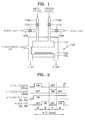
- FIG. 1shows a deposition chamber of a chemical vapor deposition (CVD) apparatus for depositing a metal nitride film on a semiconductor substrate, according to the present invention
- FIG. 2shows gas inflow timings for depositing a metal nitride film on a semiconductor substrate, according to the present invention
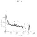
- FIG. 3is a graph of the results of Rutherford back scattering (RBS) of a metal nitride film deposited according to the present invention
- FIG. 4is a graph illustrating the resistivity and deposition speed of a metal nitride film with respect to flow amount of NH3, when the metal nitride film is deposited according to the present invention
- FIG. 5is a graph illustrating the resistivity and deposition speed of a metal nitride film with respect to pressure in a deposition chamber, when the metal nitride film is deposited according to the present invention
- FIG. 6is a graph illustrating the deposited thickness of a metal nitride film versus the number of cycles when the metal nitride film is deposited according to the present invention
- FIG. 7is a graph illustrating the deposition speed of a metal nitride film versus the number of cycles when the metal nitride film is deposited according to the present invention
- FIG. 8is a graph illustrating the resistivity of a metal nitride film versus deposition temperature when the metal nitride film is deposited according to the present invention
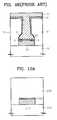
- FIGS. 9A and 9Bare cross-sections of a via contact formed by a conventional method
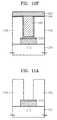
- FIGS. 10A through 10Fare cross-sectional views illustrating an example of a process for forming a via contact using the metal nitride film formation method of the present invention
- FIGS. 11A through 11Fare cross-sectional views illustrating another example of a process for forming a via contact using the metal nitride film formation method of the present invention.
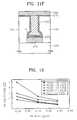
- FIG. 12is a graph illustrating the relationship between via resistivity and via width when a barrier metal layer is formed according to the present invention and the prior art
- FIG. 13is a graph illustrating via resistivity distributions when barrier metal layers are formed according to the present invention and the prior art
- FIGS. 14A through 14Dare cross-sectional views illustrating a process for forming a semiconductor capacitor using a metal nitride film formation method according to the present invention
- FIGS. 15A and 15Bare graphs showing the X-ray phonon spectroscopy (XPS) results of metal nitride films formed by a conventional method and a method according to the present invention, respectively;
- FIG. 16is a graph showing the leakage current characteristics of capacitors formed by a conventional method and a method according to the present invention.
- a plurality of gas lines 114 a and 114 b for introducing reaction gases into a deposition chamber 100are installed into the deposition chamber 100 .
- the number of gas linesdepends on the number of metal sources and nitrogen sources, i.e., the number of reaction gases, flowed into the deposition chamber 100 .
- two gas lines 114 a and 114 bare installed.
- the two gas lines 114 a and 114 bhave one end connected to a supply source (not shown) for a metal source and to a supply source (not shown) for a nitrogen source, respectively.
- a TiN filmis deposited on a semiconductor substrate 104
- TiCl 4is used as the metal source
- NH 3is used as the nitrogen source.
- the other ends of the gas lines 114 a and 114 bare connected to a shower head 110 isolated by a predetermined distance (D of FIG. 1) from the semiconductor substrate 104 seated in the deposition chamber 100 .
- reaction gases from the gas supply sourcesenter the deposition chamber 100 via the gas lines 114 a and 11 4 b and the shower head 110 connected to the ends of the gas lines 114 a and 114 b .
- the reaction gasesreact with each other in the deposition chamber, and the resultant forms a film on the semiconductor substrate 104 .
- the shower head 110is a multi-port shower head which allows the reaction gases to enter the deposition chamber 100 in an unmixed state.
- a two-port shower headis used.
- the gas lines 114 a and 114 bare provided with purge gas supply lines 114 c and 114 d to supply to the deposition chamber 100 a purge gas for exhausting residual gases after reaction.
- Valves 112are installed on the respective gas supply lines. According to the on/off state of the valves 112 , the purge gases or reaction gases may enter into the deposition chamber 100 or be cut off.
- the valves 112such as pneumatic valves, are controlled by a programmed control unit to be periodically turned on or off.
- Reference numeral 102is a heater for heating the semiconductor substrate 104 .
- a method of depositing a metal nitride such as TiN on a semiconductor substrate seated in the deposition chamber of a CVD apparatus having such a configuration, according to the present invention,will now be described in detail referring to FIGS. 1 and 2.
- the semiconductor substrate 104is introduced into the deposition chamber 100 .
- the semiconductor substrate 104may have devices such as transistors formed on its surface (see FIG. 1).
- a metal source such as TiCl 4flows into the deposition chamber 100 for the time of tS via the metal source supply line 114 a .
- the metal sourcecan be mixed with a carrier gas such as Ar or N 2 to provide a smooth gas flow into the deposition chamber 100 .
- valves other than the valve of the gas supply line 114 a for supplying a metal sourceare in off state. Accordingly, only the metal source such as TiCl 4 flows into the deposition chamber 100 .
- a part of the entering metal sourceis chemically and physically adsorbed on the surface of the substrate 104 , and the residual remains in the deposition chamber 100 .
- only one type of gasenters the deposition chamber 100 for a predetermined time, instead of simultaneously flowing reaction gases into the deposition chamber 100 . This is called gas pulsing (see FIG. 2).
- the valve of the gas supply line 114 a for introducing the metal sourceis closed, and then the valve of the purge gas supply line 114 c is opened to introduce the purge gas such as Ar or N 2 into the deposition chamber 100 for the time of tp, thereby exhausting TiCl 4 gases from the shower head 110 and the deposition chamber 100 (in the purge gas pulsing step of FIG. 2).
- the flow of the purge gas and the pressure of the deposition chamberare appropriately controlled to prevent the metal source chemically and physically adsorbed into the semiconductor substrate from being separated and exhausted, thereby exhausting only the source gas remaining within the deposition chamber.
- the valve of the purge gas supply line 114 cis closed, and the valve of the nitrogen gas source supply line 114 b is opened to introduce a nitrogen gas such as NH 3 into the deposition chamber 100 for a time tr.
- the nitrogen gasreacts with the metal source such as TiCl 4 chemically and physically adsorbed into the substrate 104 , thus forming the metal nitride such as TiN on the semiconductor substrate 104 . That is, because of the purge gas pulsing step before the nitrogen source such as NH 3 enters into the deposition chamber 100 , the metal source such as TiCl 4 remaining in the deposition chamber 100 is exhausted via the pump (see FIG. 1).
- the nitrogen source such as NH 3does not react with the metal source such as TiCl 4 within the deposition chamber 100 , except for on the semiconductor substrate 104 .
- the metal nitrideis formed on only the semiconductor substrate 104 into which TiCl 4 and NH 3 are adsorbed (in the NH 3 pulsing step of FIG. 2).
- the carrier gas such as Ar or N 2can be mixed with the nitrogen gas such as NH 3 for a smooth gas flow into the deposition chamber 100 .
- the residual nitrogen source remaining within the deposition chamber 100 after the reaction with the metal sourceis exhausted by another purge gas pulsing step (in the purge gas pulsing step of FIG. 2).
- an atmospheric gassuch as Ar or N 2 is continuously supplied into the deposition chamber 100 .
- the metal nitride film such as TiN having a predetermined thicknessis deposited through a cycle having a sequence of the TiCl 4 pulsing step, the purge gas pulsing step, the NH 3 pulsing step, and the purge gas pulsing step.
- a deposition speedis about 20 A/cycle, and when this cycle is repeated, the thickness of a thin film is proportionally increased, so that a thin film having a desired thickness can be deposited on the semiconductor substrate 100 .
- the thickness of the metal nitride film deposited for one cycleis determined by the flow amounts of the metal source and nitrogen source entering the deposition chamber 100 , the gas pulsing times, the flow amount of the purge gas, and the purge time.
- a TiN filmis deposited by the cycles comprising the gas pulsing steps, under the following reaction conditions, on the semiconductor substrate 104 which is maintained at a temperature of 500° C. or lower by the heater 102 of FIG. 1.
- object materialTiN
- flow amount of NH 3 , pulsing time (t r ) of NH 35-30 sccm, 5 sec
- carrier gas, flow amount of carrier gasAr, 10-100 sccm
- time (t t ) for one cycle30 sec
- FIG. 3shows the results of checking the state of the TiN thin film deposited on the semiconductor substrate 104 under the aforementioned conditions using an RBS method.
- a horizontal axisindicates channels in a multi-channel analyzer (MCA), and a vertical axis indicates the standardized yields of elements detected by the MCA.
- MCAmulti-channel analyzer
- E[eV]4.05′ channel+59.4.
- FIGS. 4 and 5show the resistivity and deposition speed of the TiN film deposited according to the present invention, at various flow amounts of the nitrogen source NH 3 and pressures in the deposition chamber, respectively.
- the deposition speedincreases with an increase in the flow amount of NH 3 and the pressure in the deposition chamber, and thus the resistivity also increases. Accordingly, it is preferable that the conditions for deposition are set in consideration of the thickness and the deposition speed and resistivity of the metal nitride film required according to places to apply the metal nitride film.
- a deposition speed for each cycle, the thickness and deposition speed of a TiN film deposited according to an increase in the number of cycles, and resistivity according to a change in deposition temperature,are measured under four deposition conditions as shown in the following Table 1.
- the metal sourceis TiCl 4
- the nitrogen sourceis NH 3
- the purge gasis Ar.
- FIGS. 6 and 7show the deposition thickness and deposition speed, respectively, according to an increase in the number of cycles.
- a deposition temperatureis 500° C.
- the deposition speedincreases slowly with an increase in the number of cycles, and the deposition thickness increases in proportion to the number of cycles.
- the thickness of the TiN film to be depositedcan be controlled by adjusting the number of cycles under consistent deposition conditions.
- FIG. 8is a graph showing resistivity of the TiN film with respect to deposition temperature according to the four deposition conditions described above. It can be seen from FIG. 8 that the resistivity decreases with an increase in the deposition temperature. Particularly, it can be seen that the resistivity sharply decreases under the deposition condition (TiN 00) in which the deposition speed is high. Also, we can recognize that resistivity of 200 ⁇ -cm or less is obtained at about 500° C. under all the four deposition conditions.
- a first metal layer 210 such as Alis formed on a semiconductor substrate 200 , and a TiN film 220 is deposited as a capping film on the resultant structure, as shown in FIG. 10A.
- the TiN film 220can be deposited by sputtering.
- an interlayer insulative film 230is deposited, and a portion on which a via is to be formed is etched, thereby forming the structure of FIG. 10B.
- a thin Ti film(not shown) is formed on the resultant structure to improve attachment strength of the TiN film, before the TiN film, being a barrier metal layer, is deposited. This Ti film can also be formed by sputtering.
- the TiN film 240being a barrier metal layer, is deposited by the metal nitride film formation method of the present invention, thus forming the structure of FIG. 10C. That is, as described above, a metal source, a purge gas, and a nitrogen source flow into the deposition apparatus of FIG. 1 in the sequence of the metal source, the purge gas, the nitrogen source, and the purge gas. This is repeated until a desired thickness is obtained.
- the metal sourceis TiCl 4 and the nitrogen source is NH 3 .
- the amounts of the metal source, the nitrogen source and the purge gasare 1 to 5 sccm, 5 to 200 sccm, and 10 to 200 sccm, respectively, and the inflow times thereof are about 1 to 10 seconds.
- a deposition temperatureis 480° C. or lower, and the pressure in the deposition chamber is between 1 torr and 20 torr. If necessary, an atmospheric gas such as Ar, He, or N 2 , and a carrier gas of Ar, N 2 , etc., can be used. These deposition conditions are appropriately controlled considering the deposition apparatus, the deposition speed, the thickness of the TiN film deposited, and the resistivity of the TiN film.
- a metal plug 250 such as Wis formed by a typical method, in FIG. 10D, and a metal deposited on the upper surface of an interlayer insulative film 230 is removed by chemical mechanical polishing or etch back, in FIG. 10E. Then, when a second metal layer 260 is formed on the resultant structure as shown in FIG. 10F, interconnection between metal layers is accomplished.
- FIGS. 11A through 11Fare cross-sectional views illustrating a process for forming an anchor via contact, which is fundamentally the same as the process of FIGS. 10A through 10F except that an anchor A is formed on the lower portion of a contact hole to lower resistance by increasing a contact area as shown in FIG. 11B.
- the anchor Ais formed by wet etching the interlayer insulative film 335 after forming the contact hole as shown in FIG. 11A.
- the other stepsare the same as those of FIGS. 10A through 10F, so they will not be described again.
- a Ti filmis deposited to a thickness of 100 A on contact holes of various different widths, by sputtering. Then, as a barrier metal layer, a TiN film according to the present invention, and a collimated TiN film formed by sputtering by a conventional method, are deposited to different thicknesses, and a plug is formed of CVD-W.
- the third experimentmeasures via resistance in this case.
- the deposition conditions of the TiN film according to the present inventionare equal to the deposition conditions of TiN 00 of the aforementioned second experiment, with a deposition temperature of 450° C.
- resistivitygenerally decreases with an increase in via width as shown in FIG. 12, and resistivity decreases with decreasing the thickness of the TiN film of the present invention.
- the 100 A-thick TiN film according to the present inventionhas a similar resistance to the collimated TiN film.
- the via widthis 0.39 ⁇ m
- the above five TiN filmshave similar via resistances.
- the TiN films of the present inventionwere formed at a high deposition speed per cycle (20 A/cycle) and with large resistivity (300 ⁇ -cm at 450° C.). Accordingly, if the TiN films of the present invention are formed at a lower deposition speed and with smaller resistivity, their via resistances can be significantly improved.
- FIG. 13is a graph showing the distribution of the via resistance of each TiN film when the via width is 0.39 ⁇ m. From the graph of FIG. 13, we can recognize that the collimated TiN film and the TiN films according to the present invention are evenly distributed, without a big difference, around 1.0 ⁇ .
- the present inventionhas been described by taking as an example the method wherein the TiN film is formed as a metal nitride film by using TiCl 4 and NH 3 as a precursor.
- the present inventioncan be applied to a TiN film using TiCl 3 , TiI 4 , TiBr 2 , TiF 4 , (C 5 H 5 ) 2 TiCl 2 , ((CH 3 ) 5 C 5 ) 2 TiCl 2 , C 5 H 5 TiCl 3 , C 9 H 10 BCl 3 N 6 Ti, C 9 H 7 TiCl 3 , (C 5 (CH 3 ) 5 )TiCl 3 , TiCl 4 (NH 3 ) 2 , (CH 3 ) 5 C 5 Ti(CH 3 ) 3 , TDEAT or TDMAT instead of TiCl 4 as the precursor, and also to other metal nitride films such as TaN firm using TaBr 5 , TaCl 5 , TaF 5 , TaI5,
- a deposition temperatureis between 250° C. and 400° C. and a pressure is about 0.1 to 10 torr, in contrast with the cases using the other materials as the precursor. Since the above precursors for forming the TaN film are all solid, a solid bubbler must be used to form a source gas.
- a semiconductor capacitoris formed by sequentially stacking a lower conductive layer, a dielectric film and an upper conductive layer.
- the process for forming a lower and/or upper conductive layer to form a semiconductor capacitor according to the present inventionadopts the metal nitride film formation method according to the present invention described above. That is, as described above, a metal source, a purge gas, and a nitrogen source flow into the deposition apparatus of FIG. 1 in the sequence of the metal source, the purge gas, the nitrogen source, and the purge gas. This is repeated until a desired thickness is obtained.
- the metal sourceis TiCl 4 and the nitrogen source is NH 3 .
- the amounts of the metal source, the nitrogen source and the purge gasare 1 to 5 sccm, 5 to 200 sccm, and 10 to 200 sccm, respectively, and the inflow times thereof are about 1 to 10 seconds.
- a deposition temperatureis 480° C. or lower, and the pressure in the deposition chamber is between 1 torr and 20 torr. If necessary, an atmospheric gas such as Ar, He, or N 2 , and a carrier gas of Ar, N 2 , etc., can be used. These deposition conditions are appropriately controlled considering the deposition apparatus, the deposition speed, the thickness of the TiN film deposited, and the resistivity of the TiN film.
- TiN filmis formed as a metal nitride film by using TiCl 4 and NH 3 as a precursor.
- TaN filmis formed as a metal nitride film
- TaBr 5 , TaCl 5 , TaF 5 , TaI 5 , or (C 5 (CH 3 ) 5 )TaCl 4can be used as precursors.
- a deposition temperatureis between 250° C. and 400° C. and a pressure is about 0.1 to 10 torr. Since the above precursors for forming the TaN film are all solid, a solid bubbler must be used to form a source gas.
- FIGS. 14A through 14Dare cross-sectional views illustrating a process for forming a semiconductor capacitor having a cylindrical electrode structure for measuring step coverage and leakage current characteristics.
- an SiO 2 sacrificial oxide film 440is formed on a semiconductor substrate 400 on which a predetermined contact 420 and an etch stop film 430 are formed.
- the contact 420electrically connects the active region of the semiconductor substrate to the electrode of a capacitor via the interlayer dielectric film 410 .
- cylindrical holes 447are formed by dry etching the sacrificial oxide film 440 , and then a lower conductive layer 450 is formed by chemical vapor depositing polysilicon.
- a lower electrode 455is formed by node separating the lower conductive layer 450 , and then the sacrificial oxide film 440 of FIG. 14B remaining between the lower electrodes 455 is removed.
- a dielectric film 460is formed by chemical vapor depositing Ta 2 O 5 on the semiconductor substrate on which the lower electrode has been formed, and an upper conductive layer is formed on the dielectric film at about 480° C.
- a conventional capacitoris formed by the same method as the above-described method by which the capacitor according to the present invention is formed, except that an upper conductive layer is formed by chemical vapor depositing a TiN film at about 620° C. using TiCl 4 and NH 3 as a source gas.
- 10 sccm of TiCl 4 and 50 sccm of NH 3are used when TiN is chemical vapor deposited.
- the upper and lower thicknessesdenote the thicknesses of an upper conductive layer at portions pointed by reference characters t 1 and t 2 shown in FIG. 14D, respectively.
- the step coverage of the capacitor according to the present inventionis significantly higher than that of the capacitor having a CVD'ed TiN upper conductive layer.
- the CVD techniquecan also improve step coverage by increasing the flow ratio of TiCl 4 /H 3 , but has a drawback in that the leakage current characteristics is degraded due to an increase in the concentration of Cl remaining within a film.
- the leakage current value of the capacitor according to the present inventionis lower than that of the capacitor having a CVDed upper conductive layer (CVD-TiN) in most of an applied voltage section.
- the leakage current value of the capacitor according to the present inventionis only about 1 ⁇ 3 or ⁇ fraction (1/15) ⁇ times that of the capacitor having a CVDed upper conductive layer.
- FIGS. 15A and 15Bshow the content of Cl contained in a conductive layer formed by a method according to the present invention and the content of Cl contained in a CVDed conductive layer, respectively.
- the measurement of the Cl contentis achieved by performing XPS with respect to a TiN film formed by the metal nitride film formation method according to the present invention and a CVDed TiN film which are separately formed on SiO 2 substrates.
- the left portioncorresponds to a TiN film region
- the right portion, where etching is further progressedcorresponds to an SiO 2 substrate region.
- the Cl content of the TiN film formed by a method according to the present inventionis a maximum of 0.4 atomic % in the TiN film region, but the Cl content of the TiN film formed by CVD is a maximum of 3.9 atomic % in the TiN film region.
- the Cl content in a general capacitoris maintained below 1%.
- a metal nitride filmhas low resistivity of 200 ⁇ -cm or less even with excellent step coverage and contains only a small amount of Cl.
- the metal nitride filmcan be formed at a temperature of 500° C. or lower, and also a deposition speed, approximately 20 A/cycle, is considerably higher than that in the metal nitride film formation method using ALE with a growth speed of 0.25 A/cycle.
- the metal nitride film formation method according to the present inventioncan be used to form the electrode of a semiconductor capacitor having a three-dimensional electrode structure, leading to the formation of a semiconductor capacitor having a very low content of Cl and excellent leakage current characteristics.
Landscapes
- Chemical & Material Sciences (AREA)
- Engineering & Computer Science (AREA)
- Manufacturing & Machinery (AREA)
- Chemical Kinetics & Catalysis (AREA)
- Physics & Mathematics (AREA)
- Computer Hardware Design (AREA)
- Microelectronics & Electronic Packaging (AREA)
- Power Engineering (AREA)
- Condensed Matter Physics & Semiconductors (AREA)
- General Physics & Mathematics (AREA)
- General Chemical & Material Sciences (AREA)
- Materials Engineering (AREA)
- Mechanical Engineering (AREA)
- Metallurgy (AREA)
- Organic Chemistry (AREA)
- Inorganic Chemistry (AREA)
- Chemical Vapour Deposition (AREA)
- Electrodes Of Semiconductors (AREA)
Abstract
Description
- This application is a continuation-in-part of U.S. patent application Ser. No. 09/156,724, filed Sep. 18, 1998, entitled METHOD OF FORMING METAL NITRIDE FILM CHEMICAL VAPOR DEPOSITION AND METHOD OF FORMING METAL CONTACT OF SEMICONDUCTOR DEVICE USING THE SAMEMETHOD OF FORMING METAL NITRIDE FILM CHEMICAL VAPOR DEPOSITION AND METHOD OF FORMING METAL CONTACT OF SEMICONDUCTOR DEVICE USING THE SAME.[0001]
- 1. Field of the Invention[0002]
- The present invention relates to a method of fabricating semiconductor devices, and more particularly, to a method of forming a metal nitride film by chemical vapor deposition (CVD) where a metal source and a nitrogen source are used as a precursor, and a method of forming a metal contact and a capacitor of a semiconductor device using the above method.[0003]
- 2. Description of the Related Art[0004]
- A barrier metal layer, which prevents mutual diffusion or chemical reaction between different materials, is indispensable to stabilize the contact interfaces of semiconductor devices. In general, a metal nitride such as TiN, TaN or WN has been widely used as the barrier metal layer of semiconductor devices. Here, TiN is a representative example among the above metal nitrides.[0005]
- However, when the metal nitride film such as TiN is fabricated by sputtering, its application to highly integrated semiconductor devices is not appropriate, due to low step coverage. For an example, FIGS. 9A and 9B show the cross-section of a via contact for connection between metal wiring. FIGS. 9A and 9B show a simple via contact and an anchor via contact, respectively. The formation processes thereof are as follows. A first metal layer composed of aluminum (Al) is formed on a[0006]
semiconductor substrate 20. A TiNfilm 40 is formed as a capping film on the resultant structure by sputtering, and then an interlayerinsulative film insulative film first metal layer 30. In FIG. 9B, the step of forming an anchor A by wet etching is added. After Ti as an adhesive layer andTiN plug - Here, in a conventional method, the TiN[0007]
film - When the contact failure is avoided by increasing the deposition time to increase the thickness of the[0008]
TiN film - A general process for forming a CVD-metal nitride film uses a metal source containing chlorine (Cl), e.g., a precursor such as titanium chloride TiCl[0009]4. The CVD-metal nitride film using TiCl4as the precursor has a high step coverage of 95% or higher and is quickly deposited, but Cl remains in the metal nitride film as impurities. The Cl remaining as impurities in the metal nitride film causes corrosion of metal wiring such as Al and increases resistivity. Thus, the Cl content in the metal nitride film must be reduced and the resistivity must be lowered, by deposition at high temperature. That is, in the CVD-metal nitride film process using the metal source such as TiCl4, a deposition temperature of at least 675° C. is required to obtain resistivity of 200 μΩ-cm or less. However, a deposition temperature of 600° C. or more exceeds thermal budget and thermal stress limits which an underlayer can withstand. In particular, when the metal nitride film is deposited on an Si contact or a via contact with an Al underlayer, a deposition temperature of 480° C. or lower is required, so that a high temperature CVD-metal nitride film process cannot be used.
- A low temperature deposition CVD-metal nitride film process is possible, by adding MH (methylhydrazine, (CH[0010]3)HNNH2) to the metal source such as TiCl4, but this method has a defect in that step coverage is decreased to 70% or lower.
- Another method capable of low temperature deposition is to form a MOCVD-metal nitride film using a metalorganic precursor such as TDEAT (tetrakis diethylamino Ti, Ti(N(CH[0011]2CH3)2)4), or TDMAT (tetrakis dimethylamino Ti, Ti(N(CH3)2)4). The MOCVD-metal nitride film has no problems due to Cl and can be deposited at low temperature. However, the MOCVD-metal nitride film contains a lot of carbon (C) as impurities, giving high resistivity, and has inferior step coverage of 70% or less.
- A method of forming a metal nitride film using atomic layer epitaxy (ALE) has been tried as an alternative to deposition, in order to overcome the problems due to Cl. However, the ALE grows the metal nitride film in units of an atomic layer using only chemical absorption, and the deposition speed (0.25 A/cycle or less) is too slow to apply the ALE to mass production.[0012]
- A TiN film is also used as the electrode of a semiconductor capacitor. In particular, the TiN film is usually used in a capacitor which uses tantalum oxide (Ta[0013]2O5) as a dielectric film. Semiconductor capacitors, which use the TiN film as an electrode, also have the above-described problems.
- That is, in order for a semiconductor capacitor to have a high capacitance per unit area of a semiconductor substrate, its electrode is designed three-dimensionally, as in cylindrical capacitors. Hence, the shape of the semiconductor capacitor is so complicated that it is critical to guarantee step coverage of deposited materials as its electrode. Accordingly, a TiN electrode formed by CVD using a Cl-containing metal source having an excellent step coverage as a precursor has been used as the electrode of a capacitor. However, as described above, the CVDed TiN film provokes corrosion of metal wiring and gives high resistivity, due to a high concentration of Cl, resulting in a degradation in the leakage current characteristics of a capacitor.[0014]
- To solve the above problems, an objective of the present invention is to provide a method of forming a metal nitride film, which gives excellent step coverage even at a high deposition speed and a low temperature, low impurity concentration, and low resistivity.[0015]
- Another objective of the present invention is to provide a method of forming a metal contact having a barrier metal layer which has excellent step coverage even at a high deposition speed and a low temperature, low impurity concentration, and low resistivity, by applying the metal nitride film formation method to a metal contact of a semiconductor device.[0016]
- Still another objective of the present invention is to provide a method of forming a capacitor which gives excellent step coverage, low impurity concentration and low resistivity, using the metal nitride film formation method.[0017]
- Accordingly, to achieve the first objective, there is provided a method of forming a metal nitride film using chemical vapor deposition (CVD) in which a metal source and a nitrogen source are used as a precursor. In this method, first, a semiconductor substrate is introduced into a deposition chamber, and the metal source flows into the deposition chamber. After a predetermine time, the flow of the metal is stopped, and a purge gas is introduced into the deposition chamber. After a predetermined time, the purge gas is cut off and the nitrogen source gas flows into the deposition chamber to react with the metal source adsorbed on the semiconductor substrate. Again, after a predetermined time, the nitrogen source gas remaining in the deposition chamber is removed by cutting off the inflow of the nitrogen source gas and flowing the purge gas into the deposition chamber. Thus, the metal nitride film is formed on the semiconductor substrate.[0018]
- In the metal nitride film formation method of the present invention, a gas inflow cycle of a sequence of the metal source, the purge gas, the nitrogen source, and the purge gas, can be repeated until a metal nitride film having a desired thickness is obtained.[0019]
- Here, a titanium nitride film TiN can be formed by using TiCl[0020]4(titanium chloride), TiCl3(titanium chloride), TiI4(titanium iodide), TiBr2(titanium bromide), TiF4(titanium fluoride), (C5H5)2TiCl2(bis(cyclopentadienyl)titanium dichloride), ((CH3)5C5)2TiCl2(bis(pentamethylcyclopentadienyl) titanium dichloride), C5H5TiCl3(cyclopentadienyltitanium trichloride), C9H10BCl3N6Ti (hydrotris (1-pyrazolylborato) trichloro titanium), C9H7TiCl3(indenyltitanium trichloride), (C5(CH3)5)TiCl3(pentamethylcyclopentadienyltitanium trichloride), TiCl4(NH3)2(tetrachlorodiaminotitanium), (CH3)5C5Ti(CH3)3(trimethylpentamethylcyclopentadienyltitanium), TDEAT or TDMAT as the metal source, and using NH3as the nitrogen source. Alternatively, the tantalum nitride film TaN can be formed using a material selected from the group consisting of TaBr5(tantalum bromide), TaCl5(tantalum chloride), TaF5(tantalum fluoride), TaI5(Tantalum iodide), and(C5(CH3)5)TaCl4(pentamethylcyclopentadienyltantalum tetrachloride), as the metal source, and using NH3as the nitrogen source.
- Also, it is preferable that the purge gas is an inert gas such as Ar or N[0021]2.
- Preferably, 1-5 sccm of the metal source flows into the deposition chamber for 1 to 10 seconds, 5-200 sccm of the nitrogen source flows thereinto for 1 to 10 seconds, and 10-200 sccm of the purge gas flows thereinto for 1 to 10 seconds.[0022]
- Also, an atmospheric gas such as Ar, He and N[0023]2can be continuously flowed into the deposition chamber, to maintain a constant pressure in the deposition chamber.
- Meanwhile, when the TiN film is formed using TDEAT or TDMAT as the metal source, it is preferable to maintain the pressure in the deposition chamber to be 0.1-10 torr and the deposition temperature to be between 250° C. and 400° C. When materials other than TDEAT and TDMAT are used as the metal source, the pressure in the deposition chamber is maintained to be 1 to 20 torr and the deposition temperature is maintained to be between 400° C. and 500° C.[0024]
- To achieve the second objective, there is provided a method of forming a metal contact of a semiconductor device, wherein a first metal layer, an interlayer insulative film, a contact hole, a barrier metal layer, a metal plug, and a second metal layer are sequentially formed on a semiconductor substrate. A process for forming the barrier metal layer is as follows. A metal source flows into the semiconductor substrate having the interlayer insulative film in which the contact hole exposing the first metal layer is formed. The metal source is adsorbed to the resultant structure. After a while, the metal source remaining in the deposition chamber is removed by cutting off the inflow of the metal source and flowing a purge gas into the deposition chamber. After a predetermined time, the purge gas is cut off, and a nitrogen source flows into the deposition chamber. The nitrogen source reacts with the metal source adsorbed on the semiconductor substrate, to thus form a metal nitride film, being the barrier metal layer, on the exposed first metal layer and the contact hole. Again, after a while, the nitrogen source remaining in the deposition chamber is removed by cutting off the inflow of the nitrogen source and flowing the purge gas into the deposition chamber.[0025]
- The barrier metal layer formation process can be repeated until a barrier metal layer having a desired thickness is obtained.[0026]
- Here, a titanium nitride film TiN as the barrier metal layer is formed by using a material selected from the group consisting of TiCl[0027]4, TiCl3, TiI4, TiBr2, TiF4, (C5H5)2TiCl2, ((CH3)5C5)2TiCl2, CsH5TiCl3, C9H10BCl3N6Ti, C9H7TiCl3, (C5(CH3)5)TiCl3, TiCl4(NH3)2, (CH3)5C5Ti(CH3)3, TDEAT and TDMAT as the metal source, and using NH3as the nitrogen source. Alternatively, the tantalum nitride film TaN as the barrier metal layer is formed using a material selected from the group consisting of TaBr5, TaCl5, TaF5, TaI5, and (C5(CH3)5)TaCl4as the metal source, and NH3 as the nitrogen source.
- Also, it is preferable that the purge gas is an inert gas such as Ar or N[0028]2.
- The flow amounts and flow times of the metal source, nitrogen source, and purge gas flowing into a deposition chamber are within the same ranges as in the above-mentioned method of forming the metal nitride film.[0029]
- Also, in order to maintain a constant pressure within the deposition chamber while forming a barrier metal layer, the pressure within the deposition chamber is kept at about 0.1 to 10 torr when TDEAT or TDMAT is used as the metal source, and about 1 to 20 torr when materials other than TDEAT and TDMAT are used as the metal source. The constant pressure is maintained using an atmospheric gas such as Ar, He, or N[0030]2.
- It is preferable that a deposition temperature upon the formation of the barrier metal layer is about between 250° C. and 400° C. when TDEAT or TDMAT is used as the metal source, and between 400° C. and 500° C. when materials other than TDEAT and TDMAT are used as the metal source.[0031]
- To achieve the third objective, there is provided a method of forming a semiconductor capacitor, wherein a lower conductive layer, a dielectric film and an upper conductive layer are sequentially formed on the underlayer of a semiconductor substrate. In a process for forming the lower and/or upper conductive layer, a semiconductor substrate on which an underlayer or a dielectric film is formed is introduced into a deposition chamber, and a metal source flows into the deposition chamber. The metal source is chemically and physically adsorbed onto the substrate. After a predetermined period of time, the metal source is purged from the deposition chamber. After a predetermined period of time, a nitrogen source flows into the deposition chamber, and is chemically and physically adsorbed onto the substrate. The adsorbed metal source and nitrogen source are reacted to form a metal nitride film on the substrate. After another predetermined period of time, the nitrogen source is purged from the deposition chamber.[0032]
- The step of forming a metal nitride film can be repeated until a lower and/or upper conductive layer having a desired thickness is obtained.[0033]
- Here, when Ti is used, the metal source used to form the lower and/or upper conductive layer is selected from the group consisting of TiCl[0034]4, TiCl3, TiI4, TiBr2, TiF4, (C5H5)2TiCl2, ((CH3)5C5)2TiCI2, C5H5TiCl3, C9H10BCl3N6Ti, C9H7TiCl3, (C5(CH3)5)TiCl3, TiCl4(NH3)2, (CH3)5C5Ti(CH3)3, TDEAT and TDMAT. When Ta is used, the metal source is selected from the group consisting of TaBr5, TaCl5, TaF5, Tal5, and (C5(CH3)5)TaCl4. The nitrogen source is NH3.
- Also, it is preferable that the purge gas is an inert gas such as Ar or N[0035]2.
- The flow amounts and inflow times of a metal source, a nitrogen source and a purge gas flowing into the deposition chamber are within the same ranges as those in the metal nitride film formation method according to the present invention.[0036]
- Also, in order to maintain a constant pressure within the deposition chamber while forming a lower and/or upper conductive layer, the pressure within the deposition chamber is maintained to be about 0.1-10 torr when TDEAT or TDMAT is used as a metal source, and the pressure within the deposition chamber is maintained to be about 1-20 torr when materials other than TDEAT and TDMAT are used as the metal source. The constant pressure is maintained by the use of an atmospheric gas such as Ar, He or N[0037]2.
- Preferably, when TDEAT or TDMAT is used as the metal source, the deposition temperature in each of the steps for forming a lower conductive layer and/or an upper conductive layer is between 250° C. and 500° C. Also, preferably, when other materials are used as the metal source, the deposition temperature in each of the steps for forming a lower conductive layer and/or an upper conductive layer is between 400° C. and 500° C.[0038]
- According to the present invention, a metal nitride film having low resistivity of 200μΩ-cm or less and a low content of Cl can be obtained even with excellent step coverage. Also, a CVD-metal nitride film can be formed at a temperature of 500° C. or less even at a deposition speed of about 20 A/cycle, so that the deposition speed of the present invention is higher than that of a metal nitride film formation method using ALE having a growth speed of 0.25 A/cycle. A capacitor, in which a metal nitride film formed by the method according to the present invention is used as a lower and/or upper conductive layer, has excellent step coverage and excellent leakage current characteristics.[0039]
- The above objectives and advantages of the present invention will become more apparent by describing in detail a preferred embodiment thereof with reference to the attached drawings in which:[0040]
- FIG. 1 shows a deposition chamber of a chemical vapor deposition (CVD) apparatus for depositing a metal nitride film on a semiconductor substrate, according to the present invention;[0041]
- FIG. 2 shows gas inflow timings for depositing a metal nitride film on a semiconductor substrate, according to the present invention;[0042]
- FIG. 3 is a graph of the results of Rutherford back scattering (RBS) of a metal nitride film deposited according to the present invention;[0043]
- FIG. 4 is a graph illustrating the resistivity and deposition speed of a metal nitride film with respect to flow amount of NH3, when the metal nitride film is deposited according to the present invention;[0044]
- FIG. 5 is a graph illustrating the resistivity and deposition speed of a metal nitride film with respect to pressure in a deposition chamber, when the metal nitride film is deposited according to the present invention;[0045]
- FIG. 6 is a graph illustrating the deposited thickness of a metal nitride film versus the number of cycles when the metal nitride film is deposited according to the present invention;[0046]
- FIG. 7 is a graph illustrating the deposition speed of a metal nitride film versus the number of cycles when the metal nitride film is deposited according to the present invention;[0047]
- FIG. 8 is a graph illustrating the resistivity of a metal nitride film versus deposition temperature when the metal nitride film is deposited according to the present invention;[0048]
- FIGS. 9A and 9B are cross-sections of a via contact formed by a conventional method;[0049]
- FIGS. 10A through 10F are cross-sectional views illustrating an example of a process for forming a via contact using the metal nitride film formation method of the present invention;[0050]
- FIGS. 11A through 11F are cross-sectional views illustrating another example of a process for forming a via contact using the metal nitride film formation method of the present invention;[0051]
- FIG. 12 is a graph illustrating the relationship between via resistivity and via width when a barrier metal layer is formed according to the present invention and the prior art;[0052]
- FIG. 13 is a graph illustrating via resistivity distributions when barrier metal layers are formed according to the present invention and the prior art;[0053]
- FIGS. 14A through 14D are cross-sectional views illustrating a process for forming a semiconductor capacitor using a metal nitride film formation method according to the present invention;[0054]
- FIGS. 15A and 15B are graphs showing the X-ray phonon spectroscopy (XPS) results of metal nitride films formed by a conventional method and a method according to the present invention, respectively; and[0055]
- FIG. 16 is a graph showing the leakage current characteristics of capacitors formed by a conventional method and a method according to the present invention.[0056]
- Referring to FIG. 1, a plurality of[0057]
gas lines deposition chamber 100 are installed into thedeposition chamber 100. Here, the number of gas lines depends on the number of metal sources and nitrogen sources, i.e., the number of reaction gases, flowed into thedeposition chamber 100. In an embodiment of the present invention, twogas lines - The two[0058]
gas lines semiconductor substrate 104, TiCl4is used as the metal source and NH3is used as the nitrogen source. Meanwhile, the other ends of thegas lines shower head 110 isolated by a predetermined distance (D of FIG. 1) from thesemiconductor substrate 104 seated in thedeposition chamber 100. Accordingly, the reaction gases from the gas supply sources (not shown) enter thedeposition chamber 100 via thegas lines shower head 110 connected to the ends of thegas lines semiconductor substrate 104. - It is preferable that the[0059]
shower head 110 is a multi-port shower head which allows the reaction gases to enter thedeposition chamber 100 in an unmixed state. In this embodiment, a two-port shower head is used. Also, it is preferable that thegas lines gas supply lines Valves 112 are installed on the respective gas supply lines. According to the on/off state of thevalves 112, the purge gases or reaction gases may enter into thedeposition chamber 100 or be cut off. It is preferable that thevalves 112, such as pneumatic valves, are controlled by a programmed control unit to be periodically turned on or off.Reference numeral 102 is a heater for heating thesemiconductor substrate 104. - A method of depositing a metal nitride such as TiN on a semiconductor substrate seated in the deposition chamber of a CVD apparatus having such a configuration, according to the present invention, will now be described in detail referring to FIGS. 1 and 2.[0060]
- First, the[0061]
semiconductor substrate 104 is introduced into thedeposition chamber 100. Thesemiconductor substrate 104 may have devices such as transistors formed on its surface (see FIG. 1). - A metal source such as TiCl[0062]4flows into the
deposition chamber 100 for the time of tS via the metalsource supply line 114a. Alternatively, the metal source can be mixed with a carrier gas such as Ar or N2to provide a smooth gas flow into thedeposition chamber 100. At this time, valves other than the valve of thegas supply line 114afor supplying a metal source are in off state. Accordingly, only the metal source such as TiCl4flows into thedeposition chamber 100. At this time, a part of the entering metal source is chemically and physically adsorbed on the surface of thesubstrate 104, and the residual remains in thedeposition chamber 100. As described above, only one type of gas enters thedeposition chamber 100 for a predetermined time, instead of simultaneously flowing reaction gases into thedeposition chamber 100. This is called gas pulsing (see FIG. 2). - When inflow of the metal source into the[0063]
deposition chamber 100 is completed, the valve of thegas supply line 114afor introducing the metal source is closed, and then the valve of the purgegas supply line 114cis opened to introduce the purge gas such as Ar or N2into thedeposition chamber 100 for the time of tp, thereby exhausting TiCl4gases from theshower head 110 and the deposition chamber100 (in the purge gas pulsing step of FIG. 2). At this time, the flow of the purge gas and the pressure of the deposition chamber are appropriately controlled to prevent the metal source chemically and physically adsorbed into the semiconductor substrate from being separated and exhausted, thereby exhausting only the source gas remaining within the deposition chamber. - Then, the valve of the purge[0064]
gas supply line 114cis closed, and the valve of the nitrogen gassource supply line 114bis opened to introduce a nitrogen gas such as NH3 into thedeposition chamber 100 for a time tr. The nitrogen gas reacts with the metal source such as TiCl4chemically and physically adsorbed into thesubstrate 104, thus forming the metal nitride such as TiN on thesemiconductor substrate 104. That is, because of the purge gas pulsing step before the nitrogen source such as NH3enters into thedeposition chamber 100, the metal source such as TiCl4remaining in thedeposition chamber 100 is exhausted via the pump (see FIG. 1). Accordingly, the nitrogen source such as NH3does not react with the metal source such as TiCl4within thedeposition chamber 100, except for on thesemiconductor substrate 104. Thus, the metal nitride is formed on only thesemiconductor substrate 104 into which TiCl4and NH3are adsorbed (in the NH3 pulsing step of FIG. 2). - At this time, the carrier gas such as Ar or N[0065]2can be mixed with the nitrogen gas such as NH3 for a smooth gas flow into the
deposition chamber 100. - In a conventional method of forming a metal nitride film using ALE, only the chemically-adsorbed source remains, after purging the source physically adsorbed on the substrate. On the other hand, in the metal nitride film formation method of the present invention, the sources both physically and chemically adsorbed on the substrate remain and react. This is the fundamental difference between the prior art and the present invention.[0066]
- Next, the residual nitrogen source remaining within the[0067]
deposition chamber 100 after the reaction with the metal source is exhausted by another purge gas pulsing step (in the purge gas pulsing step of FIG. 2). - Meanwhile, while the pressure in the[0068]
deposition chamber 100 is controlled during the above-described steps, it is preferable that an atmospheric gas such as Ar or N2is continuously supplied into thedeposition chamber 100. - As described above, in the method of forming a metal nitride film using gas pulsing, according to the present invention, the metal nitride film such as TiN having a predetermined thickness is deposited through a cycle having a sequence of the TiCl[0069]4pulsing step, the purge gas pulsing step, the NH3pulsing step, and the purge gas pulsing step. Here, a deposition speed is about 20 A/cycle, and when this cycle is repeated, the thickness of a thin film is proportionally increased, so that a thin film having a desired thickness can be deposited on the
semiconductor substrate 100. Here, the thickness of the metal nitride film deposited for one cycle is determined by the flow amounts of the metal source and nitrogen source entering thedeposition chamber 100, the gas pulsing times, the flow amount of the purge gas, and the purge time. - Hereinafter, experimental examples of forming a TiN film according to the present invention will be described.[0070]
- <First Experimental Example>[0071]
- A TiN film is deposited by the cycles comprising the gas pulsing steps, under the following reaction conditions, on the[0072]
semiconductor substrate 104 which is maintained at a temperature of 500° C. or lower by theheater 102 of FIG. 1. - Deposition Conditions[0073]
- object material: TiN[0074]
- atmospheric gas: Ar[0075]
- pressure in deposition chamber: 1-20Torr[0076]
- metal source, nitrogen source: TiCl[0077]4, NH3
- flow amount of TiCl[0078]4, pulsing time (ts) of TiCl4:1-5 sccm, 5 sec
- flow amount of NH[0079]3, pulsing time (tr) of NH3: 5-30 sccm, 5 sec
- purge gas, flow amount of purge gas, purge time (t[0080]p): Ar, 10-100 sccm, 10 sec
- carrier gas, flow amount of carrier gas: Ar, 10-100 sccm[0081]
- time (t[0082]t) for one cycle: 30 sec
- FIG. 3 shows the results of checking the state of the TiN thin film deposited on the[0083]
semiconductor substrate 104 under the aforementioned conditions using an RBS method. In FIG. 3, a horizontal axis indicates channels in a multi-channel analyzer (MCA), and a vertical axis indicates the standardized yields of elements detected by the MCA. Here, the relationship between each channel and energy is given by equation, E[eV]=4.05′ channel+59.4. - The TiN film deposited on the[0084]
semiconductor substrate 104 under the aforementioned conditions has a unique gold color, and has a perfect composition of Ti:N=1:1 as shown in FIG. 3. Cl is 0.3% or less of the total elements contained in the TiN thin film, which is the detection limit by RBS, as shown in FIG. 3. Also, the resistivity of the TiN film deposited on thesemiconductor substrate 104 under the above conditions was measured as a low value of about 130 μΩ-cm. Meanwhile, according to several experiments, it was verified that the thickness of the TiN thin film deposited for each cycle must be 20 A or less to provide such an excellent thin film property. - FIGS. 4 and 5 show the resistivity and deposition speed of the TiN film deposited according to the present invention, at various flow amounts of the nitrogen source NH[0085]3and pressures in the deposition chamber, respectively. As shown in FIGS. 4 and 5, the deposition speed increases with an increase in the flow amount of NH3and the pressure in the deposition chamber, and thus the resistivity also increases. Accordingly, it is preferable that the conditions for deposition are set in consideration of the thickness and the deposition speed and resistivity of the metal nitride film required according to places to apply the metal nitride film.
- <Second Experimental Example>[0086]
- A deposition speed for each cycle, the thickness and deposition speed of a TiN film deposited according to an increase in the number of cycles, and resistivity according to a change in deposition temperature, are measured under four deposition conditions as shown in the following Table 1. Here, the metal source is TiCl[0087]4, the nitrogen source is NH3, and the purge gas is Ar.
TABLE 1 amount amount amount and amount amount of deposition and time and time time of and time atmospheric conditions of metal source of purge gas nitrogen source of purge gas pressure gas TiN 00 5 sccm, 40 sccm, 150 sccm, 40 sccm, 3 torr 50 sccm 5 sec 5 sec 5 sec 5 sec TiN 01 3 sccm, 150 sccm, 30 sccm, 150 sccm, 2 torr 30 sccm 3 sec 3 sec 3 sec 3 sec TiN 02 3 sccm, 150 sccm, 50 sccm, 150 sccm, 3 torr 30 sccm 2 sec 2 sec 2 sec 2 sec TiN 03 3 sccm, 150 sccm, 100 sccm, 150 sccm, 3 torr 30 sccm 2 sec 2 sec 2 sec 2 sec - Deposition speeds per cycle under the above deposition conditions are as follows:[0088]
- TiN 00:20 A/cycle (60 A/min, since one cycle is 20 seconds)[0089]
- TiN 01:2 A/cycle (10 A/min, since one cycle is 12 seconds)[0090]
- TiN 02:3.5 A/cycle (26.3 A/min, since one cycle is 8 seconds)[0091]
- TiN 03:6 A/cycle (45 A/min, since one cycle is 8 seconds).[0092]
- FIGS. 6 and 7 show the deposition thickness and deposition speed, respectively, according to an increase in the number of cycles. Here, a deposition temperature is 500° C. As can be seen from FIGS. 6 and 7, the deposition speed increases slowly with an increase in the number of cycles, and the deposition thickness increases in proportion to the number of cycles. Thus, the thickness of the TiN film to be deposited can be controlled by adjusting the number of cycles under consistent deposition conditions.[0093]
- FIG. 8 is a graph showing resistivity of the TiN film with respect to deposition temperature according to the four deposition conditions described above. It can be seen from FIG. 8 that the resistivity decreases with an increase in the deposition temperature. Particularly, it can be seen that the resistivity sharply decreases under the deposition condition (TiN 00) in which the deposition speed is high. Also, we can recognize that resistivity of 200μΩ-cm or less is obtained at about 500° C. under all the four deposition conditions.[0094]
- An example of applying the metal nitride film formation method of the present invention to a via contact will now be described in detail, referring to FIGS. 10A through 11F.[0095]
- First, a[0096]
first metal layer 210 such as Al is formed on asemiconductor substrate 200, and aTiN film 220 is deposited as a capping film on the resultant structure, as shown in FIG. 10A. TheTiN film 220 can be deposited by sputtering. Then, aninterlayer insulative film 230 is deposited, and a portion on which a via is to be formed is etched, thereby forming the structure of FIG. 10B. A thin Ti film (not shown) is formed on the resultant structure to improve attachment strength of the TiN film, before the TiN film, being a barrier metal layer, is deposited. This Ti film can also be formed by sputtering. - Next, the[0097]
TiN film 240, being a barrier metal layer, is deposited by the metal nitride film formation method of the present invention, thus forming the structure of FIG. 10C. That is, as described above, a metal source, a purge gas, and a nitrogen source flow into the deposition apparatus of FIG. 1 in the sequence of the metal source, the purge gas, the nitrogen source, and the purge gas. This is repeated until a desired thickness is obtained. Here, the metal source is TiCl4and the nitrogen source is NH3. The amounts of the metal source, the nitrogen source and the purge gas are 1 to 5 sccm, 5 to 200 sccm, and 10 to 200 sccm, respectively, and the inflow times thereof are about 1 to 10 seconds. A deposition temperature is 480° C. or lower, and the pressure in the deposition chamber is between 1 torr and 20 torr. If necessary, an atmospheric gas such as Ar, He, or N2, and a carrier gas of Ar, N2, etc., can be used. These deposition conditions are appropriately controlled considering the deposition apparatus, the deposition speed, the thickness of the TiN film deposited, and the resistivity of the TiN film. - A[0098]
metal plug 250 such as W is formed by a typical method, in FIG. 10D, and a metal deposited on the upper surface of aninterlayer insulative film 230 is removed by chemical mechanical polishing or etch back, in FIG. 10E. Then, when asecond metal layer 260 is formed on the resultant structure as shown in FIG. 10F, interconnection between metal layers is accomplished. - FIGS. 11A through 11F are cross-sectional views illustrating a process for forming an anchor via contact, which is fundamentally the same as the process of FIGS. 10A through 10F except that an anchor A is formed on the lower portion of a contact hole to lower resistance by increasing a contact area as shown in FIG. 11B. The anchor A is formed by wet etching the[0099]
interlayer insulative film 335 after forming the contact hole as shown in FIG. 11A. The other steps are the same as those of FIGS. 10A through 10F, so they will not be described again. - As described above, when the metal nitride film formation method of the present invention is applied to the via contact, a barrier metal layer having an excellent step coverage can be obtained at low temperature. Thus, a contact failure X such as TiFx or AlFx shown in FIGS. 9A and 9B can be prevented.[0100]
- <Third Experimental Example>[0101]
- A Ti film is deposited to a thickness of[0102]100A on contact holes of various different widths, by sputtering. Then, as a barrier metal layer, a TiN film according to the present invention, and a collimated TiN film formed by sputtering by a conventional method, are deposited to different thicknesses, and a plug is formed of CVD-W. The third experiment measures via resistance in this case. Here, the deposition conditions of the TiN film according to the present invention are equal to the deposition conditions of
TiN 00 of the aforementioned second experiment, with a deposition temperature of 450° C. - Via widths: 0.24 μm, 0.32 μm, 0.39 μm (via depth: 0.9 μm) Thickness of TiN film: 100 A, 200 A, 400 A, 600 A (these are deposited by the method of the present invention), 700 A (collimated TiN film)[0103]
- As the results of measurement, resistivity generally decreases with an increase in via width as shown in FIG. 12, and resistivity decreases with decreasing the thickness of the TiN film of the present invention. The 100 A-thick TiN film according to the present invention has a similar resistance to the collimated TiN film. In particular, when the via width is 0.39 μm, the above five TiN films have similar via resistances. Meanwhile, in the second experiment and as shown in FIG. 8, the TiN films of the present invention were formed at a high deposition speed per cycle (20 A/cycle) and with large resistivity (300 μΩ-cm at 450° C.). Accordingly, if the TiN films of the present invention are formed at a lower deposition speed and with smaller resistivity, their via resistances can be significantly improved.[0104]
- FIG. 13 is a graph showing the distribution of the via resistance of each TiN film when the via width is 0.39 μm. From the graph of FIG. 13, we can recognize that the collimated TiN film and the TiN films according to the present invention are evenly distributed, without a big difference, around 1.0 Ω.[0105]
- Up to now, the present invention has been described by taking as an example the method wherein the TiN film is formed as a metal nitride film by using TiCl[0106]4and NH3as a precursor. However, the present invention can be applied to a TiN film using TiCl3, TiI4, TiBr2, TiF4, (C5H5)2TiCl2, ((CH3)5C5)2TiCl2, C5H5TiCl3, C9H10BCl3N6Ti, C9H7TiCl3, (C5(CH3)5)TiCl3, TiCl4(NH3)2, (CH3)5C5Ti(CH3)3, TDEAT or TDMAT instead of TiCl4as the precursor, and also to other metal nitride films such as TaN firm using TaBr5, TaCl5, TaF5, TaI5, or (C5(CH3)5)TaCl4as precursors, and further to almost any material layers deposited using CVD.
- However, when the TiN film is formed using TDEAT or TDMAT as the precursor, it is preferable that a deposition temperature is between 250° C. and 400° C. and a pressure is about 0.1 to 10 torr, in contrast with the cases using the other materials as the precursor. Since the above precursors for forming the TaN film are all solid, a solid bubbler must be used to form a source gas.[0107]
- An example of forming a semiconductor capacitor by applying the metal nitride formation method according to the present invention to a capacitor electrode will now be described in detail with reference to FIGS. 14 through 16.[0108]
- A semiconductor capacitor is formed by sequentially stacking a lower conductive layer, a dielectric film and an upper conductive layer. The process for forming a lower and/or upper conductive layer to form a semiconductor capacitor according to the present invention adopts the metal nitride film formation method according to the present invention described above. That is, as described above, a metal source, a purge gas, and a nitrogen source flow into the deposition apparatus of FIG. 1 in the sequence of the metal source, the purge gas, the nitrogen source, and the purge gas. This is repeated until a desired thickness is obtained. Here, the metal source is TiCl[0109]4and the nitrogen source is NH3. The amounts of the metal source, the nitrogen source and the purge gas are 1 to 5 sccm, 5 to 200 sccm, and 10 to 200 sccm, respectively, and the inflow times thereof are about 1 to 10 seconds. A deposition temperature is 480° C. or lower, and the pressure in the deposition chamber is between 1 torr and 20 torr. If necessary, an atmospheric gas such as Ar, He, or N2, and a carrier gas of Ar, N2, etc., can be used. These deposition conditions are appropriately controlled considering the deposition apparatus, the deposition speed, the thickness of the TiN film deposited, and the resistivity of the TiN film.
- Up to now, the present invention has been described by taking as an example the method wherein the TiN film is formed as a metal nitride film by using TiCl[0110]4and NH3as a precursor. However, TiCl3, TiI4, TiBr2, TiF4, (C5H5)2TiCl2, ((CH3)5C5)2TiCl2, C5H5TiCl3, C9H10BCl3N6Ti, C9H7TiCl3, (C5(CH3)5)TiCl3, TiCl4(NH3)2, (CH3)5C5Ti(CH3)3, TDEAT or TDMAT can be used as the precursor. In case that a TaN film is formed as a metal nitride film, TaBr5, TaCl5, TaF5, TaI5, or (C5(CH3)5)TaCl4can be used as precursors.
- When the TiN film is formed using TDEAT or TDMAT as the precursor, it is preferable that a deposition temperature is between 250° C. and 400° C. and a pressure is about 0.1 to 10 torr. Since the above precursors for forming the TaN film are all solid, a solid bubbler must be used to form a source gas.[0111]
- <Fourth Experimental Example>[0112]
- FIGS. 14A through 14D are cross-sectional views illustrating a process for forming a semiconductor capacitor having a cylindrical electrode structure for measuring step coverage and leakage current characteristics. Referring to FIG. 14A, an SiO[0113]2
sacrificial oxide film 440 is formed on asemiconductor substrate 400 on which apredetermined contact 420 and anetch stop film 430 are formed. Thecontact 420 electrically connects the active region of the semiconductor substrate to the electrode of a capacitor via theinterlayer dielectric film 410. - Referring to FIG. 14B,[0114]
cylindrical holes 447 are formed by dry etching thesacrificial oxide film 440, and then a lowerconductive layer 450 is formed by chemical vapor depositing polysilicon. Continuously, as shown in FIG. 14C, alower electrode 455 is formed by node separating the lowerconductive layer 450, and then thesacrificial oxide film 440 of FIG. 14B remaining between thelower electrodes 455 is removed. Next, as shown in FIG. 14D, adielectric film 460 is formed by chemical vapor depositing Ta2O5on the semiconductor substrate on which the lower electrode has been formed, and an upper conductive layer is formed on the dielectric film at about 480° C. using TiCl4nitrogen precursor and an NH3nitrogen source by the metal nitride film formation method according to the present invention. Thereafter, a polysilicon film is formed on the upper conductive layer, thereby forming the structure of a capacitor according to the present invention. A conventional capacitor is formed by the same method as the above-described method by which the capacitor according to the present invention is formed, except that an upper conductive layer is formed by chemical vapor depositing a TiN film at about 620° C. using TiCl4and NH3as a source gas. Here, 10 sccm of TiCl4and 50 sccm of NH3are used when TiN is chemical vapor deposited. - As to the capacitor formed by a method according to the present invention (expressed as SLD-TiN) and the capacitor having a chemically vapor deposited (CVDed) TiN upper conductive layer (expressed as CVD-TiN), the step coverage of an upper conductive layer and the leakage current characteristics are measured and shown in Table 2 and FIG. 16, respectively.[0115]
TABLE 2 Classification Lower thickness Upper thickness Step coverage CVD-TiN 35A 156A 22.6% SLD-TiN 188A 208A 90.1% - In Table 2, the upper and lower thicknesses denote the thicknesses of an upper conductive layer at portions pointed by reference characters t[0116]1and t2shown in FIG. 14D, respectively. As can be seen from Table 2, the step coverage of the capacitor according to the present invention is significantly higher than that of the capacitor having a CVD'ed TiN upper conductive layer. The CVD technique can also improve step coverage by increasing the flow ratio of TiCl4/H3, but has a drawback in that the leakage current characteristics is degraded due to an increase in the concentration of Cl remaining within a film.
- In FIG. 16, the leakage current value of the capacitor according to the present invention (SLD-TiN) is lower than that of the capacitor having a CVDed upper conductive layer (CVD-TiN) in most of an applied voltage section. In particular, around ±1.2 V, which is the basis of the leakage current characteristics of a capacitor, the leakage current value of the capacitor according to the present invention is only about ⅓ or {fraction (1/15)} times that of the capacitor having a CVDed upper conductive layer.[0117]
- FIGS. 15A and 15B show the content of Cl contained in a conductive layer formed by a method according to the present invention and the content of Cl contained in a CVDed conductive layer, respectively. The measurement of the Cl content is achieved by performing XPS with respect to a TiN film formed by the metal nitride film formation method according to the present invention and a CVDed TiN film which are separately formed on SiO[0118]2substrates. In the graphs of FIGS. 15A and 15B, the left portion corresponds to a TiN film region, and the right portion, where etching is further progressed, corresponds to an SiO2substrate region. As shown in FIGS. 15A and 15B, the Cl content of the TiN film formed by a method according to the present invention is a maximum of 0.4 atomic % in the TiN film region, but the Cl content of the TiN film formed by CVD is a maximum of 3.9 atomic % in the TiN film region. Preferably, the Cl content in a general capacitor is maintained below 1%. Thus, it can be seen that the TiN film formed by a method according to the present invention has a Cl content that is suitable for the conductive layer of a semiconductor capacitor.
- According to the metal nitride film fonnation method of the present invention as described above, a metal nitride film has low resistivity of 200 μΩ-cm or less even with excellent step coverage and contains only a small amount of Cl. Also, the metal nitride film can be formed at a temperature of 500° C. or lower, and also a deposition speed, approximately 20 A/cycle, is considerably higher than that in the metal nitride film formation method using ALE with a growth speed of 0.25 A/cycle.[0119]
- Accordingly, as opposed to when a metal nitride film is deposited at a temperature of 650° C. or higher in a conventional method, corrosion of metal wiring and high resistivity due to impurities (Cl) remaining in the metal nitride film can be solved, so that the present invention is applicable to a via contact which has a high aspect ratio and requires a low temperature. Also, since the present invention has a higher deposition speed than the metal nitride film formation method using ALE, it is suitable for mass production.[0120]
- Also, the metal nitride film formation method according to the present invention can be used to form the electrode of a semiconductor capacitor having a three-dimensional electrode structure, leading to the formation of a semiconductor capacitor having a very low content of Cl and excellent leakage current characteristics.[0121]
Claims (11)
1. A method of forming a semiconductor capacitor by sequentially forming a lower conductive layer, a dielectric film and an upper conductive layer on the underlayer of a semiconductor substrate, wherein the process for forming a lower conductive layer and/or an upper conductive layer comprises the steps of:
(a) inserting a semiconductor substrate on which the underlayer on the dielectric film is formed, into a deposition chamber;
(b) admitting a metal source into the deposition chamber
(c) chemisorbing a first portion of the metal source onto the substrate, and physisorbing a second portion of the metal source onto the substrate;
(d) purging the metal source from the deposition chamber;
(e) admitting a nitrogen source into the deposition chamber;
(f) chemisorbing a first portion of the nitrogen source onto the substrate, and physisorbing a second portion of the nitrogen source onto the substrate;
(g) reacting the chemisorbed and physisorbed metal source with the chemisorbed and physisorbed nitrogen source to form a metal nitride film on the substrate; and
(h) purging the nitrogen source from the deposition chamber.
2. The method as claimed in
claim 1
3. The method as claimed in
claim 2
4. The method as claimed in
claim 1
5. The method as claimed in
claim 4
6. The method as claimed in
claim 1
7. The method as claimed in
claim 6
8. The method as claimed in
claim 1
9. The method as claimed in
claim 1
10. The method as claimed in
claim 1
11. The method as claimed in
claim 1
Priority Applications (1)
| Application Number | Priority Date | Filing Date | Title |
|---|---|---|---|
| US09/765,531US6348376B2 (en) | 1997-09-29 | 2001-01-19 | Method of forming metal nitride film by chemical vapor deposition and method of forming metal contact and capacitor of semiconductor device using the same |
Applications Claiming Priority (6)
| Application Number | Priority Date | Filing Date | Title |
|---|---|---|---|
| KR19970049746 | 1997-09-29 | ||
| KR97-49746 | 1997-09-29 | ||
| KR98-29581 | 1998-07-22 | ||
| KR1019980029531AKR100304694B1 (en) | 1997-09-29 | 1998-07-22 | Forming method of chemical vapor deposited metal nitride film and forming method of metal contact in semiconductor device by using the same |
| US09/156,724US6197683B1 (en) | 1997-09-29 | 1998-09-18 | Method of forming metal nitride film by chemical vapor deposition and method of forming metal contact of semiconductor device using the same |
| US09/765,531US6348376B2 (en) | 1997-09-29 | 2001-01-19 | Method of forming metal nitride film by chemical vapor deposition and method of forming metal contact and capacitor of semiconductor device using the same |
Related Parent Applications (1)
| Application Number | Title | Priority Date | Filing Date |
|---|---|---|---|
| US09/156,724Continuation-In-PartUS6197683B1 (en) | 1997-09-29 | 1998-09-18 | Method of forming metal nitride film by chemical vapor deposition and method of forming metal contact of semiconductor device using the same |
Publications (2)
| Publication Number | Publication Date |
|---|---|
| US20010034097A1true US20010034097A1 (en) | 2001-10-25 |
| US6348376B2 US6348376B2 (en) | 2002-02-19 |
Family
ID=27349608
Family Applications (1)
| Application Number | Title | Priority Date | Filing Date |
|---|---|---|---|
| US09/765,531Expired - LifetimeUS6348376B2 (en) | 1997-09-29 | 2001-01-19 | Method of forming metal nitride film by chemical vapor deposition and method of forming metal contact and capacitor of semiconductor device using the same |
Country Status (1)
| Country | Link |
|---|---|
| US (1) | US6348376B2 (en) |
Cited By (335)
| Publication number | Priority date | Publication date | Assignee | Title |
|---|---|---|---|---|
| US6743473B1 (en)* | 2000-02-16 | 2004-06-01 | Applied Materials, Inc. | Chemical vapor deposition of barriers from novel precursors |
| US20040235191A1 (en)* | 2001-09-03 | 2004-11-25 | Toshio Hasegawa | Film forming method |
| US20050106877A1 (en)* | 1999-10-15 | 2005-05-19 | Kai-Erik Elers | Method for depositing nanolaminate thin films on sensitive surfaces |
| US20050260811A1 (en)* | 2004-05-20 | 2005-11-24 | Taiwan Semiconductor Manufacturing Co., Ltd. | Low temperature method for metal deposition |
| US20060068104A1 (en)* | 2003-06-16 | 2006-03-30 | Tokyo Electron Limited | Thin-film formation in semiconductor device fabrication process and film deposition apparatus |
| US20060151852A1 (en)* | 2002-07-19 | 2006-07-13 | Yoshihide Senzaki | In-situ formation of metal insulator metal capacitors cross reference to related applications |
| US20060193980A1 (en)* | 2003-02-20 | 2006-08-31 | Toshio Hasegawa | Method for forming film |
| US20070160757A1 (en)* | 2002-10-03 | 2007-07-12 | Tokyo Electron Limited | Processing method |
| US20070200243A1 (en)* | 2005-07-20 | 2007-08-30 | Micron Technology, Inc. | Ald formed titanium nitride films |
| US20120219710A1 (en)* | 2011-02-28 | 2012-08-30 | Tokyo Electron Limited | Method of forming titanium nitride film, apparatus for forming titanium nitride film, and program |
| US8841182B1 (en) | 2013-03-14 | 2014-09-23 | Asm Ip Holding B.V. | Silane and borane treatments for titanium carbide films |
| US8846550B1 (en) | 2013-03-14 | 2014-09-30 | Asm Ip Holding B.V. | Silane or borane treatment of metal thin films |
| US8993055B2 (en) | 2005-10-27 | 2015-03-31 | Asm International N.V. | Enhanced thin film deposition |
| US9394609B2 (en) | 2014-02-13 | 2016-07-19 | Asm Ip Holding B.V. | Atomic layer deposition of aluminum fluoride thin films |
| US9631272B2 (en) | 2008-04-16 | 2017-04-25 | Asm America, Inc. | Atomic layer deposition of metal carbide films using aluminum hydrocarbon compounds |
| US9704716B2 (en) | 2013-03-13 | 2017-07-11 | Asm Ip Holding B.V. | Deposition of smooth metal nitride films |
| US9786491B2 (en) | 2015-11-12 | 2017-10-10 | Asm Ip Holding B.V. | Formation of SiOCN thin films |
| US9786492B2 (en) | 2015-11-12 | 2017-10-10 | Asm Ip Holding B.V. | Formation of SiOCN thin films |
| US9941425B2 (en) | 2015-10-16 | 2018-04-10 | Asm Ip Holdings B.V. | Photoactive devices and materials |
| US20180114722A1 (en)* | 2016-10-25 | 2018-04-26 | Kwang Chul PARK | Deposition apparatus including uv annealing unit and method for fabricating non-volatile memory device by using the deposition apparatus |
| US10002936B2 (en) | 2014-10-23 | 2018-06-19 | Asm Ip Holding B.V. | Titanium aluminum and tantalum aluminum thin films |
| US10186420B2 (en) | 2016-11-29 | 2019-01-22 | Asm Ip Holding B.V. | Formation of silicon-containing thin films |
| US10236517B2 (en)* | 2017-08-16 | 2019-03-19 | GM Global Technology Operations LLC | Method for manufacturing and cleaning a stainless steel fuel cell bipolar plate |
| US20190304790A1 (en)* | 2018-03-27 | 2019-10-03 | Asm Ip Holding B.V. | Method of forming an electrode on a substrate and a semiconductor device structure including an electrode |
| US10504901B2 (en) | 2017-04-26 | 2019-12-10 | Asm Ip Holding B.V. | Substrate processing method and device manufactured using the same |
| US10600637B2 (en) | 2016-05-06 | 2020-03-24 | Asm Ip Holding B.V. | Formation of SiOC thin films |
| US10643925B2 (en) | 2014-04-17 | 2020-05-05 | Asm Ip Holding B.V. | Fluorine-containing conductive films |
| US10720331B2 (en) | 2016-11-01 | 2020-07-21 | ASM IP Holdings, B.V. | Methods for forming a transition metal nitride film on a substrate by atomic layer deposition and related semiconductor device structures |
| US10767789B2 (en) | 2018-07-16 | 2020-09-08 | Asm Ip Holding B.V. | Diaphragm valves, valve components, and methods for forming valve components |
| US10784102B2 (en) | 2016-12-22 | 2020-09-22 | Asm Ip Holding B.V. | Method of forming a structure on a substrate |
| US10787741B2 (en) | 2014-08-21 | 2020-09-29 | Asm Ip Holding B.V. | Method and system for in situ formation of gas-phase compounds |
| US10797133B2 (en) | 2018-06-21 | 2020-10-06 | Asm Ip Holding B.V. | Method for depositing a phosphorus doped silicon arsenide film and related semiconductor device structures |
| US10804098B2 (en) | 2009-08-14 | 2020-10-13 | Asm Ip Holding B.V. | Systems and methods for thin-film deposition of metal oxides using excited nitrogen-oxygen species |
| US10818758B2 (en) | 2018-11-16 | 2020-10-27 | Asm Ip Holding B.V. | Methods for forming a metal silicate film on a substrate in a reaction chamber and related semiconductor device structures |
| US10832903B2 (en) | 2011-10-28 | 2020-11-10 | Asm Ip Holding B.V. | Process feed management for semiconductor substrate processing |
| US10829852B2 (en) | 2018-08-16 | 2020-11-10 | Asm Ip Holding B.V. | Gas distribution device for a wafer processing apparatus |
| US10847529B2 (en) | 2017-04-13 | 2020-11-24 | Asm Ip Holding B.V. | Substrate processing method and device manufactured by the same |
| US10844484B2 (en) | 2017-09-22 | 2020-11-24 | Asm Ip Holding B.V. | Apparatus for dispensing a vapor phase reactant to a reaction chamber and related methods |
| US10847366B2 (en) | 2018-11-16 | 2020-11-24 | Asm Ip Holding B.V. | Methods for depositing a transition metal chalcogenide film on a substrate by a cyclical deposition process |
| US10844486B2 (en) | 2009-04-06 | 2020-11-24 | Asm Ip Holding B.V. | Semiconductor processing reactor and components thereof |
| US10851456B2 (en) | 2016-04-21 | 2020-12-01 | Asm Ip Holding B.V. | Deposition of metal borides |
| US10858737B2 (en) | 2014-07-28 | 2020-12-08 | Asm Ip Holding B.V. | Showerhead assembly and components thereof |
| US10865475B2 (en) | 2016-04-21 | 2020-12-15 | Asm Ip Holding B.V. | Deposition of metal borides and silicides |
| US10867788B2 (en) | 2016-12-28 | 2020-12-15 | Asm Ip Holding B.V. | Method of forming a structure on a substrate |
| US10867786B2 (en) | 2018-03-30 | 2020-12-15 | Asm Ip Holding B.V. | Substrate processing method |
| US10872771B2 (en) | 2018-01-16 | 2020-12-22 | Asm Ip Holding B. V. | Method for depositing a material film on a substrate within a reaction chamber by a cyclical deposition process and related device structures |
| US10883175B2 (en) | 2018-08-09 | 2021-01-05 | Asm Ip Holding B.V. | Vertical furnace for processing substrates and a liner for use therein |
| US10886123B2 (en) | 2017-06-02 | 2021-01-05 | Asm Ip Holding B.V. | Methods for forming low temperature semiconductor layers and related semiconductor device structures |
| TWI715787B (en)* | 2016-07-05 | 2021-01-11 | 日商Adeka股份有限公司 | Raw material for forming thin film and method for manufacturing thin film |
| US10892156B2 (en) | 2017-05-08 | 2021-01-12 | Asm Ip Holding B.V. | Methods for forming a silicon nitride film on a substrate and related semiconductor device structures |
| US10896820B2 (en) | 2018-02-14 | 2021-01-19 | Asm Ip Holding B.V. | Method for depositing a ruthenium-containing film on a substrate by a cyclical deposition process |
| TWI717530B (en)* | 2016-07-05 | 2021-02-01 | 日商Adeka股份有限公司 | Method manufacturing thin film containing metal carbide |
| US10910262B2 (en) | 2017-11-16 | 2021-02-02 | Asm Ip Holding B.V. | Method of selectively depositing a capping layer structure on a semiconductor device structure |
| US10914004B2 (en) | 2018-06-29 | 2021-02-09 | Asm Ip Holding B.V. | Thin-film deposition method and manufacturing method of semiconductor device |
| US10923344B2 (en) | 2017-10-30 | 2021-02-16 | Asm Ip Holding B.V. | Methods for forming a semiconductor structure and related semiconductor structures |
| US10928731B2 (en) | 2017-09-21 | 2021-02-23 | Asm Ip Holding B.V. | Method of sequential infiltration synthesis treatment of infiltrateable material and structures and devices formed using same |
| US10934619B2 (en) | 2016-11-15 | 2021-03-02 | Asm Ip Holding B.V. | Gas supply unit and substrate processing apparatus including the gas supply unit |
| US10943771B2 (en) | 2016-10-26 | 2021-03-09 | Asm Ip Holding B.V. | Methods for thermally calibrating reaction chambers |
| US10941490B2 (en) | 2014-10-07 | 2021-03-09 | Asm Ip Holding B.V. | Multiple temperature range susceptor, assembly, reactor and system including the susceptor, and methods of using the same |
| US10950432B2 (en) | 2017-04-25 | 2021-03-16 | Asm Ip Holding B.V. | Method of depositing thin film and method of manufacturing semiconductor device |
| USD913980S1 (en) | 2018-02-01 | 2021-03-23 | Asm Ip Holding B.V. | Gas supply plate for semiconductor manufacturing apparatus |
| US10975470B2 (en) | 2018-02-23 | 2021-04-13 | Asm Ip Holding B.V. | Apparatus for detecting or monitoring for a chemical precursor in a high temperature environment |
| US10991573B2 (en) | 2017-12-04 | 2021-04-27 | Asm Ip Holding B.V. | Uniform deposition of SiOC on dielectric and metal surfaces |
| US11004676B2 (en) | 2015-03-30 | 2021-05-11 | Kokusai Electric Corporation | Method for manufacturing semiconductor device, non-transitory computer-readable recording medium, and substrate processing apparatus |
| US11004977B2 (en) | 2017-07-19 | 2021-05-11 | Asm Ip Holding B.V. | Method for depositing a group IV semiconductor and related semiconductor device structures |
| US11001925B2 (en) | 2016-12-19 | 2021-05-11 | Asm Ip Holding B.V. | Substrate processing apparatus |
| US11015245B2 (en) | 2014-03-19 | 2021-05-25 | Asm Ip Holding B.V. | Gas-phase reactor and system having exhaust plenum and components thereof |
| US11018047B2 (en) | 2018-01-25 | 2021-05-25 | Asm Ip Holding B.V. | Hybrid lift pin |
| US11018002B2 (en) | 2017-07-19 | 2021-05-25 | Asm Ip Holding B.V. | Method for selectively depositing a Group IV semiconductor and related semiconductor device structures |
| US11024523B2 (en) | 2018-09-11 | 2021-06-01 | Asm Ip Holding B.V. | Substrate processing apparatus and method |
| US11022879B2 (en) | 2017-11-24 | 2021-06-01 | Asm Ip Holding B.V. | Method of forming an enhanced unexposed photoresist layer |
| US11031242B2 (en) | 2018-11-07 | 2021-06-08 | Asm Ip Holding B.V. | Methods for depositing a boron doped silicon germanium film |
| USD922229S1 (en) | 2019-06-05 | 2021-06-15 | Asm Ip Holding B.V. | Device for controlling a temperature of a gas supply unit |
| US11049751B2 (en) | 2018-09-14 | 2021-06-29 | Asm Ip Holding B.V. | Cassette supply system to store and handle cassettes and processing apparatus equipped therewith |
| US11053591B2 (en) | 2018-08-06 | 2021-07-06 | Asm Ip Holding B.V. | Multi-port gas injection system and reactor system including same |
| US11056567B2 (en) | 2018-05-11 | 2021-07-06 | Asm Ip Holding B.V. | Method of forming a doped metal carbide film on a substrate and related semiconductor device structures |
| US11056344B2 (en) | 2017-08-30 | 2021-07-06 | Asm Ip Holding B.V. | Layer forming method |
| US11069510B2 (en) | 2017-08-30 | 2021-07-20 | Asm Ip Holding B.V. | Substrate processing apparatus |
| US11081345B2 (en) | 2018-02-06 | 2021-08-03 | Asm Ip Holding B.V. | Method of post-deposition treatment for silicon oxide film |
| US11087997B2 (en) | 2018-10-31 | 2021-08-10 | Asm Ip Holding B.V. | Substrate processing apparatus for processing substrates |
| US11088002B2 (en) | 2018-03-29 | 2021-08-10 | Asm Ip Holding B.V. | Substrate rack and a substrate processing system and method |
| US11094546B2 (en) | 2017-10-05 | 2021-08-17 | Asm Ip Holding B.V. | Method for selectively depositing a metallic film on a substrate |
| US11094582B2 (en) | 2016-07-08 | 2021-08-17 | Asm Ip Holding B.V. | Selective deposition method to form air gaps |
| US11101370B2 (en) | 2016-05-02 | 2021-08-24 | Asm Ip Holding B.V. | Method of forming a germanium oxynitride film |
| US11107676B2 (en) | 2016-07-28 | 2021-08-31 | Asm Ip Holding B.V. | Method and apparatus for filling a gap |
| US11114294B2 (en) | 2019-03-08 | 2021-09-07 | Asm Ip Holding B.V. | Structure including SiOC layer and method of forming same |
| US11114283B2 (en) | 2018-03-16 | 2021-09-07 | Asm Ip Holding B.V. | Reactor, system including the reactor, and methods of manufacturing and using same |
| USD930782S1 (en) | 2019-08-22 | 2021-09-14 | Asm Ip Holding B.V. | Gas distributor |
| US11127589B2 (en) | 2019-02-01 | 2021-09-21 | Asm Ip Holding B.V. | Method of topology-selective film formation of silicon oxide |
| US11127617B2 (en) | 2017-11-27 | 2021-09-21 | Asm Ip Holding B.V. | Storage device for storing wafer cassettes for use with a batch furnace |
| USD931978S1 (en) | 2019-06-27 | 2021-09-28 | Asm Ip Holding B.V. | Showerhead vacuum transport |
| US11139191B2 (en) | 2017-08-09 | 2021-10-05 | Asm Ip Holding B.V. | Storage apparatus for storing cassettes for substrates and processing apparatus equipped therewith |
| US11139308B2 (en) | 2015-12-29 | 2021-10-05 | Asm Ip Holding B.V. | Atomic layer deposition of III-V compounds to form V-NAND devices |
| US11158513B2 (en) | 2018-12-13 | 2021-10-26 | Asm Ip Holding B.V. | Methods for forming a rhenium-containing film on a substrate by a cyclical deposition process and related semiconductor device structures |
| US11158500B2 (en) | 2017-05-05 | 2021-10-26 | Asm Ip Holding B.V. | Plasma enhanced deposition processes for controlled formation of oxygen containing thin films |
| US11164955B2 (en) | 2017-07-18 | 2021-11-02 | Asm Ip Holding B.V. | Methods for forming a semiconductor device structure and related semiconductor device structures |
| USD935572S1 (en) | 2019-05-24 | 2021-11-09 | Asm Ip Holding B.V. | Gas channel plate |
| US11168395B2 (en) | 2018-06-29 | 2021-11-09 | Asm Ip Holding B.V. | Temperature-controlled flange and reactor system including same |
| US11171025B2 (en) | 2019-01-22 | 2021-11-09 | Asm Ip Holding B.V. | Substrate processing device |
| US11205585B2 (en) | 2016-07-28 | 2021-12-21 | Asm Ip Holding B.V. | Substrate processing apparatus and method of operating the same |
| US11217444B2 (en) | 2018-11-30 | 2022-01-04 | Asm Ip Holding B.V. | Method for forming an ultraviolet radiation responsive metal oxide-containing film |
| USD940837S1 (en) | 2019-08-22 | 2022-01-11 | Asm Ip Holding B.V. | Electrode |
| US11222772B2 (en) | 2016-12-14 | 2022-01-11 | Asm Ip Holding B.V. | Substrate processing apparatus |
| US11227782B2 (en) | 2019-07-31 | 2022-01-18 | Asm Ip Holding B.V. | Vertical batch furnace assembly |
| US11227789B2 (en) | 2019-02-20 | 2022-01-18 | Asm Ip Holding B.V. | Method and apparatus for filling a recess formed within a substrate surface |
| US11233133B2 (en) | 2015-10-21 | 2022-01-25 | Asm Ip Holding B.V. | NbMC layers |
| US11232963B2 (en) | 2018-10-03 | 2022-01-25 | Asm Ip Holding B.V. | Substrate processing apparatus and method |
| US11230766B2 (en) | 2018-03-29 | 2022-01-25 | Asm Ip Holding B.V. | Substrate processing apparatus and method |
| US11242598B2 (en) | 2015-06-26 | 2022-02-08 | Asm Ip Holding B.V. | Structures including metal carbide material, devices including the structures, and methods of forming same |
| US11251040B2 (en) | 2019-02-20 | 2022-02-15 | Asm Ip Holding B.V. | Cyclical deposition method including treatment step and apparatus for same |
| US11251068B2 (en) | 2018-10-19 | 2022-02-15 | Asm Ip Holding B.V. | Substrate processing apparatus and substrate processing method |
| USD944946S1 (en) | 2019-06-14 | 2022-03-01 | Asm Ip Holding B.V. | Shower plate |
| US11270899B2 (en) | 2018-06-04 | 2022-03-08 | Asm Ip Holding B.V. | Wafer handling chamber with moisture reduction |
| US11274369B2 (en) | 2018-09-11 | 2022-03-15 | Asm Ip Holding B.V. | Thin film deposition method |
| US11282698B2 (en) | 2019-07-19 | 2022-03-22 | Asm Ip Holding B.V. | Method of forming topology-controlled amorphous carbon polymer film |
| US11286562B2 (en) | 2018-06-08 | 2022-03-29 | Asm Ip Holding B.V. | Gas-phase chemical reactor and method of using same |
| US11289326B2 (en) | 2019-05-07 | 2022-03-29 | Asm Ip Holding B.V. | Method for reforming amorphous carbon polymer film |
| US11286558B2 (en) | 2019-08-23 | 2022-03-29 | Asm Ip Holding B.V. | Methods for depositing a molybdenum nitride film on a surface of a substrate by a cyclical deposition process and related semiconductor device structures including a molybdenum nitride film |
| US11295980B2 (en) | 2017-08-30 | 2022-04-05 | Asm Ip Holding B.V. | Methods for depositing a molybdenum metal film over a dielectric surface of a substrate by a cyclical deposition process and related semiconductor device structures |
| USD947913S1 (en) | 2019-05-17 | 2022-04-05 | Asm Ip Holding B.V. | Susceptor shaft |
| USD948463S1 (en) | 2018-10-24 | 2022-04-12 | Asm Ip Holding B.V. | Susceptor for semiconductor substrate supporting apparatus |
| USD949319S1 (en) | 2019-08-22 | 2022-04-19 | Asm Ip Holding B.V. | Exhaust duct |
| US11306395B2 (en) | 2017-06-28 | 2022-04-19 | Asm Ip Holding B.V. | Methods for depositing a transition metal nitride film on a substrate by atomic layer deposition and related deposition apparatus |
| US11315794B2 (en) | 2019-10-21 | 2022-04-26 | Asm Ip Holding B.V. | Apparatus and methods for selectively etching films |
| US11342216B2 (en) | 2019-02-20 | 2022-05-24 | Asm Ip Holding B.V. | Cyclical deposition method and apparatus for filling a recess formed within a substrate surface |
| US11339476B2 (en) | 2019-10-08 | 2022-05-24 | Asm Ip Holding B.V. | Substrate processing device having connection plates, substrate processing method |
| US11345999B2 (en) | 2019-06-06 | 2022-05-31 | Asm Ip Holding B.V. | Method of using a gas-phase reactor system including analyzing exhausted gas |
| US11355338B2 (en) | 2019-05-10 | 2022-06-07 | Asm Ip Holding B.V. | Method of depositing material onto a surface and structure formed according to the method |
| US11361990B2 (en) | 2018-05-28 | 2022-06-14 | Asm Ip Holding B.V. | Substrate processing method and device manufactured by using the same |
| US11374112B2 (en) | 2017-07-19 | 2022-06-28 | Asm Ip Holding B.V. | Method for depositing a group IV semiconductor and related semiconductor device structures |
| US11378337B2 (en) | 2019-03-28 | 2022-07-05 | Asm Ip Holding B.V. | Door opener and substrate processing apparatus provided therewith |
| US11387120B2 (en) | 2017-09-28 | 2022-07-12 | Asm Ip Holding B.V. | Chemical dispensing apparatus and methods for dispensing a chemical to a reaction chamber |
| US11393690B2 (en) | 2018-01-19 | 2022-07-19 | Asm Ip Holding B.V. | Deposition method |
| US11390945B2 (en) | 2019-07-03 | 2022-07-19 | Asm Ip Holding B.V. | Temperature control assembly for substrate processing apparatus and method of using same |
| US11390946B2 (en) | 2019-01-17 | 2022-07-19 | Asm Ip Holding B.V. | Methods of forming a transition metal containing film on a substrate by a cyclical deposition process |
| US11390950B2 (en) | 2017-01-10 | 2022-07-19 | Asm Ip Holding B.V. | Reactor system and method to reduce residue buildup during a film deposition process |
| US11401605B2 (en) | 2019-11-26 | 2022-08-02 | Asm Ip Holding B.V. | Substrate processing apparatus |
| US11410851B2 (en) | 2017-02-15 | 2022-08-09 | Asm Ip Holding B.V. | Methods for forming a metallic film on a substrate by cyclical deposition and related semiconductor device structures |
| US11417545B2 (en) | 2017-08-08 | 2022-08-16 | Asm Ip Holding B.V. | Radiation shield |
| US11414760B2 (en) | 2018-10-08 | 2022-08-16 | Asm Ip Holding B.V. | Substrate support unit, thin film deposition apparatus including the same, and substrate processing apparatus including the same |
| US11424119B2 (en) | 2019-03-08 | 2022-08-23 | Asm Ip Holding B.V. | Method for selective deposition of silicon nitride layer and structure including selectively-deposited silicon nitride layer |
| US11430640B2 (en) | 2019-07-30 | 2022-08-30 | Asm Ip Holding B.V. | Substrate processing apparatus |
| US11430674B2 (en) | 2018-08-22 | 2022-08-30 | Asm Ip Holding B.V. | Sensor array, apparatus for dispensing a vapor phase reactant to a reaction chamber and related methods |
| US11437241B2 (en) | 2020-04-08 | 2022-09-06 | Asm Ip Holding B.V. | Apparatus and methods for selectively etching silicon oxide films |
| US11443926B2 (en) | 2019-07-30 | 2022-09-13 | Asm Ip Holding B.V. | Substrate processing apparatus |
| US11447864B2 (en) | 2019-04-19 | 2022-09-20 | Asm Ip Holding B.V. | Layer forming method and apparatus |
| US11447861B2 (en) | 2016-12-15 | 2022-09-20 | Asm Ip Holding B.V. | Sequential infiltration synthesis apparatus and a method of forming a patterned structure |
| USD965044S1 (en) | 2019-08-19 | 2022-09-27 | Asm Ip Holding B.V. | Susceptor shaft |
| US11453943B2 (en) | 2016-05-25 | 2022-09-27 | Asm Ip Holding B.V. | Method for forming carbon-containing silicon/metal oxide or nitride film by ALD using silicon precursor and hydrocarbon precursor |
| USD965524S1 (en) | 2019-08-19 | 2022-10-04 | Asm Ip Holding B.V. | Susceptor support |
| US11469098B2 (en) | 2018-05-08 | 2022-10-11 | Asm Ip Holding B.V. | Methods for depositing an oxide film on a substrate by a cyclical deposition process and related device structures |
| US11473195B2 (en) | 2018-03-01 | 2022-10-18 | Asm Ip Holding B.V. | Semiconductor processing apparatus and a method for processing a substrate |
| US11476109B2 (en) | 2019-06-11 | 2022-10-18 | Asm Ip Holding B.V. | Method of forming an electronic structure using reforming gas, system for performing the method, and structure formed using the method |
| US11482533B2 (en) | 2019-02-20 | 2022-10-25 | Asm Ip Holding B.V. | Apparatus and methods for plug fill deposition in 3-D NAND applications |
| US11482412B2 (en) | 2018-01-19 | 2022-10-25 | Asm Ip Holding B.V. | Method for depositing a gap-fill layer by plasma-assisted deposition |
| US11482418B2 (en) | 2018-02-20 | 2022-10-25 | Asm Ip Holding B.V. | Substrate processing method and apparatus |
| US11488819B2 (en) | 2018-12-04 | 2022-11-01 | Asm Ip Holding B.V. | Method of cleaning substrate processing apparatus |
| US11488854B2 (en) | 2020-03-11 | 2022-11-01 | Asm Ip Holding B.V. | Substrate handling device with adjustable joints |
| US11495459B2 (en) | 2019-09-04 | 2022-11-08 | Asm Ip Holding B.V. | Methods for selective deposition using a sacrificial capping layer |
| US11492703B2 (en) | 2018-06-27 | 2022-11-08 | Asm Ip Holding B.V. | Cyclic deposition methods for forming metal-containing material and films and structures including the metal-containing material |
| US11501968B2 (en) | 2019-11-15 | 2022-11-15 | Asm Ip Holding B.V. | Method for providing a semiconductor device with silicon filled gaps |
| US11501956B2 (en) | 2012-10-12 | 2022-11-15 | Asm Ip Holding B.V. | Semiconductor reaction chamber showerhead |
| US11499226B2 (en) | 2018-11-02 | 2022-11-15 | Asm Ip Holding B.V. | Substrate supporting unit and a substrate processing device including the same |
| US11499222B2 (en) | 2018-06-27 | 2022-11-15 | Asm Ip Holding B.V. | Cyclic deposition methods for forming metal-containing material and films and structures including the metal-containing material |
| US11515187B2 (en) | 2020-05-01 | 2022-11-29 | Asm Ip Holding B.V. | Fast FOUP swapping with a FOUP handler |
| US11515188B2 (en) | 2019-05-16 | 2022-11-29 | Asm Ip Holding B.V. | Wafer boat handling device, vertical batch furnace and method |
| US11521851B2 (en) | 2020-02-03 | 2022-12-06 | Asm Ip Holding B.V. | Method of forming structures including a vanadium or indium layer |
| US11527403B2 (en) | 2019-12-19 | 2022-12-13 | Asm Ip Holding B.V. | Methods for filling a gap feature on a substrate surface and related semiconductor structures |
| US11527400B2 (en) | 2019-08-23 | 2022-12-13 | Asm Ip Holding B.V. | Method for depositing silicon oxide film having improved quality by peald using bis(diethylamino)silane |
| US11530876B2 (en) | 2020-04-24 | 2022-12-20 | Asm Ip Holding B.V. | Vertical batch furnace assembly comprising a cooling gas supply |
| US11530483B2 (en) | 2018-06-21 | 2022-12-20 | Asm Ip Holding B.V. | Substrate processing system |
| US11532757B2 (en) | 2016-10-27 | 2022-12-20 | Asm Ip Holding B.V. | Deposition of charge trapping layers |
| US11551925B2 (en) | 2019-04-01 | 2023-01-10 | Asm Ip Holding B.V. | Method for manufacturing a semiconductor device |
| US11551912B2 (en) | 2020-01-20 | 2023-01-10 | Asm Ip Holding B.V. | Method of forming thin film and method of modifying surface of thin film |
| USD975665S1 (en) | 2019-05-17 | 2023-01-17 | Asm Ip Holding B.V. | Susceptor shaft |
| US11557474B2 (en) | 2019-07-29 | 2023-01-17 | Asm Ip Holding B.V. | Methods for selective deposition utilizing n-type dopants and/or alternative dopants to achieve high dopant incorporation |
| US11562901B2 (en) | 2019-09-25 | 2023-01-24 | Asm Ip Holding B.V. | Substrate processing method |
| US11572620B2 (en) | 2018-11-06 | 2023-02-07 | Asm Ip Holding B.V. | Methods for selectively depositing an amorphous silicon film on a substrate |
| US11581186B2 (en) | 2016-12-15 | 2023-02-14 | Asm Ip Holding B.V. | Sequential infiltration synthesis apparatus |
| US11587814B2 (en) | 2019-07-31 | 2023-02-21 | Asm Ip Holding B.V. | Vertical batch furnace assembly |
| US11587821B2 (en) | 2017-08-08 | 2023-02-21 | Asm Ip Holding B.V. | Substrate lift mechanism and reactor including same |
| US11587815B2 (en) | 2019-07-31 | 2023-02-21 | Asm Ip Holding B.V. | Vertical batch furnace assembly |
| US11594450B2 (en) | 2019-08-22 | 2023-02-28 | Asm Ip Holding B.V. | Method for forming a structure with a hole |
| US11594600B2 (en) | 2019-11-05 | 2023-02-28 | Asm Ip Holding B.V. | Structures with doped semiconductor layers and methods and systems for forming same |
| USD979506S1 (en) | 2019-08-22 | 2023-02-28 | Asm Ip Holding B.V. | Insulator |
| USD980813S1 (en) | 2021-05-11 | 2023-03-14 | Asm Ip Holding B.V. | Gas flow control plate for substrate processing apparatus |
| USD980814S1 (en) | 2021-05-11 | 2023-03-14 | Asm Ip Holding B.V. | Gas distributor for substrate processing apparatus |
| US11605528B2 (en) | 2019-07-09 | 2023-03-14 | Asm Ip Holding B.V. | Plasma device using coaxial waveguide, and substrate treatment method |
| US11610775B2 (en) | 2016-07-28 | 2023-03-21 | Asm Ip Holding B.V. | Method and apparatus for filling a gap |
| US11610774B2 (en) | 2019-10-02 | 2023-03-21 | Asm Ip Holding B.V. | Methods for forming a topographically selective silicon oxide film by a cyclical plasma-enhanced deposition process |
| US11615970B2 (en) | 2019-07-17 | 2023-03-28 | Asm Ip Holding B.V. | Radical assist ignition plasma system and method |
| USD981973S1 (en) | 2021-05-11 | 2023-03-28 | Asm Ip Holding B.V. | Reactor wall for substrate processing apparatus |
| US11626316B2 (en) | 2019-11-20 | 2023-04-11 | Asm Ip Holding B.V. | Method of depositing carbon-containing material on a surface of a substrate, structure formed using the method, and system for forming the structure |
| US11626308B2 (en) | 2020-05-13 | 2023-04-11 | Asm Ip Holding B.V. | Laser alignment fixture for a reactor system |
| US11629407B2 (en) | 2019-02-22 | 2023-04-18 | Asm Ip Holding B.V. | Substrate processing apparatus and method for processing substrates |
| US11629406B2 (en) | 2018-03-09 | 2023-04-18 | Asm Ip Holding B.V. | Semiconductor processing apparatus comprising one or more pyrometers for measuring a temperature of a substrate during transfer of the substrate |
| US11637011B2 (en) | 2019-10-16 | 2023-04-25 | Asm Ip Holding B.V. | Method of topology-selective film formation of silicon oxide |
| US11637014B2 (en) | 2019-10-17 | 2023-04-25 | Asm Ip Holding B.V. | Methods for selective deposition of doped semiconductor material |
| US11639548B2 (en) | 2019-08-21 | 2023-05-02 | Asm Ip Holding B.V. | Film-forming material mixed-gas forming device and film forming device |
| US11639811B2 (en) | 2017-11-27 | 2023-05-02 | Asm Ip Holding B.V. | Apparatus including a clean mini environment |
| US11646205B2 (en) | 2019-10-29 | 2023-05-09 | Asm Ip Holding B.V. | Methods of selectively forming n-type doped material on a surface, systems for selectively forming n-type doped material, and structures formed using same |
| US11646197B2 (en) | 2018-07-03 | 2023-05-09 | Asm Ip Holding B.V. | Method for depositing silicon-free carbon-containing film as gap-fill layer by pulse plasma-assisted deposition |
| US11646184B2 (en) | 2019-11-29 | 2023-05-09 | Asm Ip Holding B.V. | Substrate processing apparatus |
| US11644758B2 (en) | 2020-07-17 | 2023-05-09 | Asm Ip Holding B.V. | Structures and methods for use in photolithography |
| US11643724B2 (en) | 2019-07-18 | 2023-05-09 | Asm Ip Holding B.V. | Method of forming structures using a neutral beam |
| US11646204B2 (en) | 2020-06-24 | 2023-05-09 | Asm Ip Holding B.V. | Method for forming a layer provided with silicon |
| US11649546B2 (en) | 2016-07-08 | 2023-05-16 | Asm Ip Holding B.V. | Organic reactants for atomic layer deposition |
| US11658029B2 (en) | 2018-12-14 | 2023-05-23 | Asm Ip Holding B.V. | Method of forming a device structure using selective deposition of gallium nitride and system for same |
| US11658035B2 (en) | 2020-06-30 | 2023-05-23 | Asm Ip Holding B.V. | Substrate processing method |
| US11658030B2 (en) | 2017-03-29 | 2023-05-23 | Asm Ip Holding B.V. | Method for forming doped metal oxide films on a substrate by cyclical deposition and related semiconductor device structures |
| US11664245B2 (en) | 2019-07-16 | 2023-05-30 | Asm Ip Holding B.V. | Substrate processing device |
| US11664199B2 (en) | 2018-10-19 | 2023-05-30 | Asm Ip Holding B.V. | Substrate processing apparatus and substrate processing method |
| US11664267B2 (en) | 2019-07-10 | 2023-05-30 | Asm Ip Holding B.V. | Substrate support assembly and substrate processing device including the same |
| US11674220B2 (en) | 2020-07-20 | 2023-06-13 | Asm Ip Holding B.V. | Method for depositing molybdenum layers using an underlayer |
| US11676812B2 (en) | 2016-02-19 | 2023-06-13 | Asm Ip Holding B.V. | Method for forming silicon nitride film selectively on top/bottom portions |
| US11680839B2 (en) | 2019-08-05 | 2023-06-20 | Asm Ip Holding B.V. | Liquid level sensor for a chemical source vessel |
| US11685991B2 (en) | 2018-02-14 | 2023-06-27 | Asm Ip Holding B.V. | Method for depositing a ruthenium-containing film on a substrate by a cyclical deposition process |
| USD990534S1 (en) | 2020-09-11 | 2023-06-27 | Asm Ip Holding B.V. | Weighted lift pin |
| US11688603B2 (en) | 2019-07-17 | 2023-06-27 | Asm Ip Holding B.V. | Methods of forming silicon germanium structures |
| USD990441S1 (en) | 2021-09-07 | 2023-06-27 | Asm Ip Holding B.V. | Gas flow control plate |
| US11705333B2 (en) | 2020-05-21 | 2023-07-18 | Asm Ip Holding B.V. | Structures including multiple carbon layers and methods of forming and using same |
| US11718913B2 (en) | 2018-06-04 | 2023-08-08 | Asm Ip Holding B.V. | Gas distribution system and reactor system including same |
| US11725280B2 (en) | 2020-08-26 | 2023-08-15 | Asm Ip Holding B.V. | Method for forming metal silicon oxide and metal silicon oxynitride layers |
| US11725277B2 (en) | 2011-07-20 | 2023-08-15 | Asm Ip Holding B.V. | Pressure transmitter for a semiconductor processing environment |
| US11735422B2 (en) | 2019-10-10 | 2023-08-22 | Asm Ip Holding B.V. | Method of forming a photoresist underlayer and structure including same |
| US11742198B2 (en) | 2019-03-08 | 2023-08-29 | Asm Ip Holding B.V. | Structure including SiOCN layer and method of forming same |
| US11742189B2 (en) | 2015-03-12 | 2023-08-29 | Asm Ip Holding B.V. | Multi-zone reactor, system including the reactor, and method of using the same |
| US11767589B2 (en) | 2020-05-29 | 2023-09-26 | Asm Ip Holding B.V. | Substrate processing device |
| US11769682B2 (en) | 2017-08-09 | 2023-09-26 | Asm Ip Holding B.V. | Storage apparatus for storing cassettes for substrates and processing apparatus equipped therewith |
| US11776846B2 (en) | 2020-02-07 | 2023-10-03 | Asm Ip Holding B.V. | Methods for depositing gap filling fluids and related systems and devices |
| US11781221B2 (en) | 2019-05-07 | 2023-10-10 | Asm Ip Holding B.V. | Chemical source vessel with dip tube |
| US11781243B2 (en) | 2020-02-17 | 2023-10-10 | Asm Ip Holding B.V. | Method for depositing low temperature phosphorous-doped silicon |
| US11804364B2 (en) | 2020-05-19 | 2023-10-31 | Asm Ip Holding B.V. | Substrate processing apparatus |
| US11802338B2 (en) | 2017-07-26 | 2023-10-31 | Asm Ip Holding B.V. | Chemical treatment, deposition and/or infiltration apparatus and method for using the same |
| US11810788B2 (en) | 2016-11-01 | 2023-11-07 | Asm Ip Holding B.V. | Methods for forming a transition metal niobium nitride film on a substrate by atomic layer deposition and related semiconductor device structures |
| US11814747B2 (en) | 2019-04-24 | 2023-11-14 | Asm Ip Holding B.V. | Gas-phase reactor system-with a reaction chamber, a solid precursor source vessel, a gas distribution system, and a flange assembly |
| US11821078B2 (en) | 2020-04-15 | 2023-11-21 | Asm Ip Holding B.V. | Method for forming precoat film and method for forming silicon-containing film |
| US11823876B2 (en) | 2019-09-05 | 2023-11-21 | Asm Ip Holding B.V. | Substrate processing apparatus |
| US11823866B2 (en) | 2020-04-02 | 2023-11-21 | Asm Ip Holding B.V. | Thin film forming method |
| US11830730B2 (en) | 2017-08-29 | 2023-11-28 | Asm Ip Holding B.V. | Layer forming method and apparatus |
| US11827981B2 (en) | 2020-10-14 | 2023-11-28 | Asm Ip Holding B.V. | Method of depositing material on stepped structure |
| US11830738B2 (en) | 2020-04-03 | 2023-11-28 | Asm Ip Holding B.V. | Method for forming barrier layer and method for manufacturing semiconductor device |
| US11828707B2 (en) | 2020-02-04 | 2023-11-28 | Asm Ip Holding B.V. | Method and apparatus for transmittance measurements of large articles |
| US11840761B2 (en) | 2019-12-04 | 2023-12-12 | Asm Ip Holding B.V. | Substrate processing apparatus |
| US11848200B2 (en) | 2017-05-08 | 2023-12-19 | Asm Ip Holding B.V. | Methods for selectively forming a silicon nitride film on a substrate and related semiconductor device structures |
| US20230420490A1 (en)* | 2019-10-21 | 2023-12-28 | Samsung Electronics Co., Ltd. | Method of manufacturing metal nitride film and electronic device including metal nitride film |
| US11873557B2 (en) | 2020-10-22 | 2024-01-16 | Asm Ip Holding B.V. | Method of depositing vanadium metal |
| US11876356B2 (en) | 2020-03-11 | 2024-01-16 | Asm Ip Holding B.V. | Lockout tagout assembly and system and method of using same |
| USD1012873S1 (en) | 2020-09-24 | 2024-01-30 | Asm Ip Holding B.V. | Electrode for semiconductor processing apparatus |
| US11885023B2 (en) | 2018-10-01 | 2024-01-30 | Asm Ip Holding B.V. | Substrate retaining apparatus, system including the apparatus, and method of using same |
| US11887857B2 (en) | 2020-04-24 | 2024-01-30 | Asm Ip Holding B.V. | Methods and systems for depositing a layer comprising vanadium, nitrogen, and a further element |
| US11885013B2 (en) | 2019-12-17 | 2024-01-30 | Asm Ip Holding B.V. | Method of forming vanadium nitride layer and structure including the vanadium nitride layer |
| US11885020B2 (en) | 2020-12-22 | 2024-01-30 | Asm Ip Holding B.V. | Transition metal deposition method |
| US11891696B2 (en) | 2020-11-30 | 2024-02-06 | Asm Ip Holding B.V. | Injector configured for arrangement within a reaction chamber of a substrate processing apparatus |
| US11901179B2 (en) | 2020-10-28 | 2024-02-13 | Asm Ip Holding B.V. | Method and device for depositing silicon onto substrates |
| US11898243B2 (en) | 2020-04-24 | 2024-02-13 | Asm Ip Holding B.V. | Method of forming vanadium nitride-containing layer |
| US11915929B2 (en) | 2019-11-26 | 2024-02-27 | Asm Ip Holding B.V. | Methods for selectively forming a target film on a substrate comprising a first dielectric surface and a second metallic surface |
| US11923181B2 (en) | 2019-11-29 | 2024-03-05 | Asm Ip Holding B.V. | Substrate processing apparatus for minimizing the effect of a filling gas during substrate processing |
| US11923190B2 (en) | 2018-07-03 | 2024-03-05 | Asm Ip Holding B.V. | Method for depositing silicon-free carbon-containing film as gap-fill layer by pulse plasma-assisted deposition |
| US11929251B2 (en) | 2019-12-02 | 2024-03-12 | Asm Ip Holding B.V. | Substrate processing apparatus having electrostatic chuck and substrate processing method |
| US11946137B2 (en) | 2020-12-16 | 2024-04-02 | Asm Ip Holding B.V. | Runout and wobble measurement fixtures |
| US11961741B2 (en) | 2020-03-12 | 2024-04-16 | Asm Ip Holding B.V. | Method for fabricating layer structure having target topological profile |
| US11959168B2 (en) | 2020-04-29 | 2024-04-16 | Asm Ip Holding B.V. | Solid source precursor vessel |
| USD1023959S1 (en) | 2021-05-11 | 2024-04-23 | Asm Ip Holding B.V. | Electrode for substrate processing apparatus |
| US11967488B2 (en) | 2013-02-01 | 2024-04-23 | Asm Ip Holding B.V. | Method for treatment of deposition reactor |
| US11976359B2 (en) | 2020-01-06 | 2024-05-07 | Asm Ip Holding B.V. | Gas supply assembly, components thereof, and reactor system including same |
| US11986868B2 (en) | 2020-02-28 | 2024-05-21 | Asm Ip Holding B.V. | System dedicated for parts cleaning |
| US11987881B2 (en) | 2020-05-22 | 2024-05-21 | Asm Ip Holding B.V. | Apparatus for depositing thin films using hydrogen peroxide |
| US11996309B2 (en) | 2019-05-16 | 2024-05-28 | Asm Ip Holding B.V. | Wafer boat handling device, vertical batch furnace and method |
| US11996289B2 (en) | 2020-04-16 | 2024-05-28 | Asm Ip Holding B.V. | Methods of forming structures including silicon germanium and silicon layers, devices formed using the methods, and systems for performing the methods |
| US11993847B2 (en) | 2020-01-08 | 2024-05-28 | Asm Ip Holding B.V. | Injector |
| US11996292B2 (en) | 2019-10-25 | 2024-05-28 | Asm Ip Holding B.V. | Methods for filling a gap feature on a substrate surface and related semiconductor structures |
| US11993843B2 (en) | 2017-08-31 | 2024-05-28 | Asm Ip Holding B.V. | Substrate processing apparatus |
| US12009224B2 (en) | 2020-09-29 | 2024-06-11 | Asm Ip Holding B.V. | Apparatus and method for etching metal nitrides |
| US12006572B2 (en) | 2019-10-08 | 2024-06-11 | Asm Ip Holding B.V. | Reactor system including a gas distribution assembly for use with activated species and method of using same |
| US12009241B2 (en) | 2019-10-14 | 2024-06-11 | Asm Ip Holding B.V. | Vertical batch furnace assembly with detector to detect cassette |
| US12020934B2 (en) | 2020-07-08 | 2024-06-25 | Asm Ip Holding B.V. | Substrate processing method |
| US12027365B2 (en) | 2020-11-24 | 2024-07-02 | Asm Ip Holding B.V. | Methods for filling a gap and related systems and devices |
| US12025484B2 (en) | 2018-05-08 | 2024-07-02 | Asm Ip Holding B.V. | Thin film forming method |
| US12033885B2 (en) | 2020-01-06 | 2024-07-09 | Asm Ip Holding B.V. | Channeled lift pin |
| US12040199B2 (en) | 2018-11-28 | 2024-07-16 | Asm Ip Holding B.V. | Substrate processing apparatus for processing substrates |
| US12040200B2 (en) | 2017-06-20 | 2024-07-16 | Asm Ip Holding B.V. | Semiconductor processing apparatus and methods for calibrating a semiconductor processing apparatus |
| US12040177B2 (en) | 2020-08-18 | 2024-07-16 | Asm Ip Holding B.V. | Methods for forming a laminate film by cyclical plasma-enhanced deposition processes |
| US12051602B2 (en) | 2020-05-04 | 2024-07-30 | Asm Ip Holding B.V. | Substrate processing system for processing substrates with an electronics module located behind a door in a front wall of the substrate processing system |
| US12051567B2 (en) | 2020-10-07 | 2024-07-30 | Asm Ip Holding B.V. | Gas supply unit and substrate processing apparatus including gas supply unit |
| US12057314B2 (en) | 2020-05-15 | 2024-08-06 | Asm Ip Holding B.V. | Methods for silicon germanium uniformity control using multiple precursors |
| US12074022B2 (en) | 2020-08-27 | 2024-08-27 | Asm Ip Holding B.V. | Method and system for forming patterned structures using multiple patterning process |
| US12087586B2 (en) | 2020-04-15 | 2024-09-10 | Asm Ip Holding B.V. | Method of forming chromium nitride layer and structure including the chromium nitride layer |
| US12107005B2 (en) | 2020-10-06 | 2024-10-01 | Asm Ip Holding B.V. | Deposition method and an apparatus for depositing a silicon-containing material |
| US12106944B2 (en) | 2020-06-02 | 2024-10-01 | Asm Ip Holding B.V. | Rotating substrate support |
| US12112940B2 (en) | 2019-07-19 | 2024-10-08 | Asm Ip Holding B.V. | Method of forming topology-controlled amorphous carbon polymer film |
| US12125700B2 (en) | 2020-01-16 | 2024-10-22 | Asm Ip Holding B.V. | Method of forming high aspect ratio features |
| US12129545B2 (en) | 2020-12-22 | 2024-10-29 | Asm Ip Holding B.V. | Precursor capsule, a vessel and a method |
| US12131885B2 (en) | 2020-12-22 | 2024-10-29 | Asm Ip Holding B.V. | Plasma treatment device having matching box |
| US12142479B2 (en) | 2020-01-17 | 2024-11-12 | Asm Ip Holding B.V. | Formation of SiOCN thin films |
| US12148609B2 (en) | 2020-09-16 | 2024-11-19 | Asm Ip Holding B.V. | Silicon oxide deposition method |
| US12154824B2 (en) | 2020-08-14 | 2024-11-26 | Asm Ip Holding B.V. | Substrate processing method |
| US12159788B2 (en) | 2020-12-14 | 2024-12-03 | Asm Ip Holding B.V. | Method of forming structures for threshold voltage control |
| US12169361B2 (en) | 2019-07-30 | 2024-12-17 | Asm Ip Holding B.V. | Substrate processing apparatus and method |
| US12173402B2 (en) | 2018-02-15 | 2024-12-24 | Asm Ip Holding B.V. | Method of forming a transition metal containing film on a substrate by a cyclical deposition process, a method for supplying a transition metal halide compound to a reaction chamber, and related vapor deposition apparatus |
| US12173404B2 (en) | 2020-03-17 | 2024-12-24 | Asm Ip Holding B.V. | Method of depositing epitaxial material, structure formed using the method, and system for performing the method |
| US12195852B2 (en) | 2020-11-23 | 2025-01-14 | Asm Ip Holding B.V. | Substrate processing apparatus with an injector |
| US12209308B2 (en) | 2020-11-12 | 2025-01-28 | Asm Ip Holding B.V. | Reactor and related methods |
| US12211742B2 (en) | 2020-09-10 | 2025-01-28 | Asm Ip Holding B.V. | Methods for depositing gap filling fluid |
| US12217954B2 (en) | 2020-08-25 | 2025-02-04 | Asm Ip Holding B.V. | Method of cleaning a surface |
| US12217946B2 (en) | 2020-10-15 | 2025-02-04 | Asm Ip Holding B.V. | Method of manufacturing semiconductor device, and substrate treatment apparatus using ether-CAT |
| US12218000B2 (en) | 2020-09-25 | 2025-02-04 | Asm Ip Holding B.V. | Semiconductor processing method |
| USD1060598S1 (en) | 2021-12-03 | 2025-02-04 | Asm Ip Holding B.V. | Split showerhead cover |
| US12218269B2 (en) | 2020-02-13 | 2025-02-04 | Asm Ip Holding B.V. | Substrate processing apparatus including light receiving device and calibration method of light receiving device |
| US12221357B2 (en) | 2020-04-24 | 2025-02-11 | Asm Ip Holding B.V. | Methods and apparatus for stabilizing vanadium compounds |
| US12230531B2 (en) | 2018-04-09 | 2025-02-18 | Asm Ip Holding B.V. | Substrate supporting apparatus, substrate processing apparatus including the same, and substrate processing method |
| US12243757B2 (en) | 2020-05-21 | 2025-03-04 | Asm Ip Holding B.V. | Flange and apparatus for processing substrates |
| US12241158B2 (en) | 2020-07-20 | 2025-03-04 | Asm Ip Holding B.V. | Method for forming structures including transition metal layers |
| US12243747B2 (en) | 2020-04-24 | 2025-03-04 | Asm Ip Holding B.V. | Methods of forming structures including vanadium boride and vanadium phosphide layers |
| US12243742B2 (en) | 2020-04-21 | 2025-03-04 | Asm Ip Holding B.V. | Method for processing a substrate |
| US12240760B2 (en) | 2016-03-18 | 2025-03-04 | Asm Ip Holding B.V. | Aligned carbon nanotubes |
| US12247286B2 (en) | 2019-08-09 | 2025-03-11 | Asm Ip Holding B.V. | Heater assembly including cooling apparatus and method of using same |
| US12252785B2 (en) | 2019-06-10 | 2025-03-18 | Asm Ip Holding B.V. | Method for cleaning quartz epitaxial chambers |
| US12255053B2 (en) | 2020-12-10 | 2025-03-18 | Asm Ip Holding B.V. | Methods and systems for depositing a layer |
| US12266524B2 (en) | 2020-06-16 | 2025-04-01 | Asm Ip Holding B.V. | Method for depositing boron containing silicon germanium layers |
| US12272527B2 (en) | 2018-05-09 | 2025-04-08 | Asm Ip Holding B.V. | Apparatus for use with hydrogen radicals and method of using same |
| US12278129B2 (en) | 2020-03-04 | 2025-04-15 | Asm Ip Holding B.V. | Alignment fixture for a reactor system |
| US12276023B2 (en) | 2017-08-04 | 2025-04-15 | Asm Ip Holding B.V. | Showerhead assembly for distributing a gas within a reaction chamber |
| US12288710B2 (en) | 2020-12-18 | 2025-04-29 | Asm Ip Holding B.V. | Wafer processing apparatus with a rotatable table |
| US12322591B2 (en) | 2020-07-27 | 2025-06-03 | Asm Ip Holding B.V. | Thin film deposition process |
| US12341005B2 (en) | 2020-01-17 | 2025-06-24 | Asm Ip Holding B.V. | Formation of SiCN thin films |
| US12354877B2 (en) | 2020-06-24 | 2025-07-08 | Asm Ip Holding B.V. | Vapor deposition of films comprising molybdenum |
| US12359315B2 (en) | 2019-02-14 | 2025-07-15 | Asm Ip Holding B.V. | Deposition of oxides and nitrides |
| US12378665B2 (en) | 2018-10-26 | 2025-08-05 | Asm Ip Holding B.V. | High temperature coatings for a preclean and etch apparatus and related methods |
| US12406846B2 (en) | 2020-05-26 | 2025-09-02 | Asm Ip Holding B.V. | Method for depositing boron and gallium containing silicon germanium layers |
| US12410515B2 (en) | 2020-01-29 | 2025-09-09 | Asm Ip Holding B.V. | Contaminant trap system for a reactor system |
| US12428726B2 (en) | 2019-10-08 | 2025-09-30 | Asm Ip Holding B.V. | Gas injection system and reactor system including same |
| US12431354B2 (en) | 2020-07-01 | 2025-09-30 | Asm Ip Holding B.V. | Silicon nitride and silicon oxide deposition methods using fluorine inhibitor |
| US12431334B2 (en) | 2020-02-13 | 2025-09-30 | Asm Ip Holding B.V. | Gas distribution assembly |
| US12444599B2 (en) | 2021-12-08 | 2025-10-14 | Asm Ip Holding B.V. | Method for forming an ultraviolet radiation responsive metal oxide-containing film |
Families Citing this family (111)
| Publication number | Priority date | Publication date | Assignee | Title |
|---|---|---|---|---|
| US6974766B1 (en) | 1998-10-01 | 2005-12-13 | Applied Materials, Inc. | In situ deposition of a low κ dielectric layer, barrier layer, etch stop, and anti-reflective coating for damascene application |
| US6319766B1 (en) | 2000-02-22 | 2001-11-20 | Applied Materials, Inc. | Method of tantalum nitride deposition by tantalum oxide densification |
| US6620723B1 (en)* | 2000-06-27 | 2003-09-16 | Applied Materials, Inc. | Formation of boride barrier layers using chemisorption techniques |
| US6551929B1 (en)* | 2000-06-28 | 2003-04-22 | Applied Materials, Inc. | Bifurcated deposition process for depositing refractory metal layers employing atomic layer deposition and chemical vapor deposition techniques |
| US7101795B1 (en) | 2000-06-28 | 2006-09-05 | Applied Materials, Inc. | Method and apparatus for depositing refractory metal layers employing sequential deposition techniques to form a nucleation layer |
| US6936538B2 (en)* | 2001-07-16 | 2005-08-30 | Applied Materials, Inc. | Method and apparatus for depositing tungsten after surface treatment to improve film characteristics |
| US7405158B2 (en)* | 2000-06-28 | 2008-07-29 | Applied Materials, Inc. | Methods for depositing tungsten layers employing atomic layer deposition techniques |
| US20020036780A1 (en)* | 2000-09-27 | 2002-03-28 | Hiroaki Nakamura | Image processing apparatus |
| US6596643B2 (en)* | 2001-05-07 | 2003-07-22 | Applied Materials, Inc. | CVD TiSiN barrier for copper integration |
| US6686278B2 (en)* | 2001-06-19 | 2004-02-03 | United Microelectronics Corp. | Method for forming a plug metal layer |
| US6849545B2 (en)* | 2001-06-20 | 2005-02-01 | Applied Materials, Inc. | System and method to form a composite film stack utilizing sequential deposition techniques |
| US20030029715A1 (en)* | 2001-07-25 | 2003-02-13 | Applied Materials, Inc. | An Apparatus For Annealing Substrates In Physical Vapor Deposition Systems |
| US20090004850A1 (en) | 2001-07-25 | 2009-01-01 | Seshadri Ganguli | Process for forming cobalt and cobalt silicide materials in tungsten contact applications |
| US8110489B2 (en)* | 2001-07-25 | 2012-02-07 | Applied Materials, Inc. | Process for forming cobalt-containing materials |
| US9051641B2 (en)* | 2001-07-25 | 2015-06-09 | Applied Materials, Inc. | Cobalt deposition on barrier surfaces |
| JP2005504885A (en) | 2001-07-25 | 2005-02-17 | アプライド マテリアルズ インコーポレイテッド | Barrier formation using a novel sputter deposition method |
| US20080268635A1 (en)* | 2001-07-25 | 2008-10-30 | Sang-Ho Yu | Process for forming cobalt and cobalt silicide materials in copper contact applications |
| US6718126B2 (en) | 2001-09-14 | 2004-04-06 | Applied Materials, Inc. | Apparatus and method for vaporizing solid precursor for CVD or atomic layer deposition |
| US7049226B2 (en)* | 2001-09-26 | 2006-05-23 | Applied Materials, Inc. | Integration of ALD tantalum nitride for copper metallization |
| US20030059538A1 (en)* | 2001-09-26 | 2003-03-27 | Applied Materials, Inc. | Integration of barrier layer and seed layer |
| US6936906B2 (en)* | 2001-09-26 | 2005-08-30 | Applied Materials, Inc. | Integration of barrier layer and seed layer |
| US7780785B2 (en) | 2001-10-26 | 2010-08-24 | Applied Materials, Inc. | Gas delivery apparatus for atomic layer deposition |
| US6916398B2 (en)* | 2001-10-26 | 2005-07-12 | Applied Materials, Inc. | Gas delivery apparatus and method for atomic layer deposition |
| US6773507B2 (en)* | 2001-12-06 | 2004-08-10 | Applied Materials, Inc. | Apparatus and method for fast-cycle atomic layer deposition |
| US7081271B2 (en)* | 2001-12-07 | 2006-07-25 | Applied Materials, Inc. | Cyclical deposition of refractory metal silicon nitride |
| US6939801B2 (en)* | 2001-12-21 | 2005-09-06 | Applied Materials, Inc. | Selective deposition of a barrier layer on a dielectric material |
| US6911391B2 (en) | 2002-01-26 | 2005-06-28 | Applied Materials, Inc. | Integration of titanium and titanium nitride layers |
| US6998014B2 (en)* | 2002-01-26 | 2006-02-14 | Applied Materials, Inc. | Apparatus and method for plasma assisted deposition |
| US6833161B2 (en)* | 2002-02-26 | 2004-12-21 | Applied Materials, Inc. | Cyclical deposition of tungsten nitride for metal oxide gate electrode |
| US6972267B2 (en) | 2002-03-04 | 2005-12-06 | Applied Materials, Inc. | Sequential deposition of tantalum nitride using a tantalum-containing precursor and a nitrogen-containing precursor |
| US6846516B2 (en)* | 2002-04-08 | 2005-01-25 | Applied Materials, Inc. | Multiple precursor cyclical deposition system |
| US6720027B2 (en)* | 2002-04-08 | 2004-04-13 | Applied Materials, Inc. | Cyclical deposition of a variable content titanium silicon nitride layer |
| US7279432B2 (en)* | 2002-04-16 | 2007-10-09 | Applied Materials, Inc. | System and method for forming an integrated barrier layer |
| US7041335B2 (en)* | 2002-06-04 | 2006-05-09 | Applied Materials, Inc. | Titanium tantalum nitride silicide layer |
| US6838125B2 (en)* | 2002-07-10 | 2005-01-04 | Applied Materials, Inc. | Method of film deposition using activated precursor gases |
| US20040013803A1 (en)* | 2002-07-16 | 2004-01-22 | Applied Materials, Inc. | Formation of titanium nitride films using a cyclical deposition process |
| US6955211B2 (en) | 2002-07-17 | 2005-10-18 | Applied Materials, Inc. | Method and apparatus for gas temperature control in a semiconductor processing system |
| US7186385B2 (en)* | 2002-07-17 | 2007-03-06 | Applied Materials, Inc. | Apparatus for providing gas to a processing chamber |
| US7066194B2 (en)* | 2002-07-19 | 2006-06-27 | Applied Materials, Inc. | Valve design and configuration for fast delivery system |
| US6772072B2 (en)* | 2002-07-22 | 2004-08-03 | Applied Materials, Inc. | Method and apparatus for monitoring solid precursor delivery |
| US6915592B2 (en) | 2002-07-29 | 2005-07-12 | Applied Materials, Inc. | Method and apparatus for generating gas to a processing chamber |
| US6821563B2 (en) | 2002-10-02 | 2004-11-23 | Applied Materials, Inc. | Gas distribution system for cyclical layer deposition |
| US20040065255A1 (en)* | 2002-10-02 | 2004-04-08 | Applied Materials, Inc. | Cyclical layer deposition system |
| US6905737B2 (en)* | 2002-10-11 | 2005-06-14 | Applied Materials, Inc. | Method of delivering activated species for rapid cyclical deposition |
| EP1420080A3 (en) | 2002-11-14 | 2005-11-09 | Applied Materials, Inc. | Apparatus and method for hybrid chemical deposition processes |
| US7244683B2 (en)* | 2003-01-07 | 2007-07-17 | Applied Materials, Inc. | Integration of ALD/CVD barriers with porous low k materials |
| US7262133B2 (en) | 2003-01-07 | 2007-08-28 | Applied Materials, Inc. | Enhancement of copper line reliability using thin ALD tan film to cap the copper line |
| US6753248B1 (en) | 2003-01-27 | 2004-06-22 | Applied Materials, Inc. | Post metal barrier/adhesion film |
| US7211508B2 (en)* | 2003-06-18 | 2007-05-01 | Applied Materials, Inc. | Atomic layer deposition of tantalum based barrier materials |
| US7048968B2 (en)* | 2003-08-22 | 2006-05-23 | Micron Technology, Inc. | Methods of depositing materials over substrates, and methods of forming layers over substrates |
| US20050067103A1 (en)* | 2003-09-26 | 2005-03-31 | Applied Materials, Inc. | Interferometer endpoint monitoring device |
| US20050252449A1 (en) | 2004-05-12 | 2005-11-17 | Nguyen Son T | Control of gas flow and delivery to suppress the formation of particles in an MOCVD/ALD system |
| US8323754B2 (en)* | 2004-05-21 | 2012-12-04 | Applied Materials, Inc. | Stabilization of high-k dielectric materials |
| US20060019033A1 (en)* | 2004-05-21 | 2006-01-26 | Applied Materials, Inc. | Plasma treatment of hafnium-containing materials |
| US20060062917A1 (en)* | 2004-05-21 | 2006-03-23 | Shankar Muthukrishnan | Vapor deposition of hafnium silicate materials with tris(dimethylamino)silane |
| US20060153995A1 (en)* | 2004-05-21 | 2006-07-13 | Applied Materials, Inc. | Method for fabricating a dielectric stack |
| US7211509B1 (en)* | 2004-06-14 | 2007-05-01 | Novellus Systems, Inc, | Method for enhancing the nucleation and morphology of ruthenium films on dielectric substrates using amine containing compounds |
| US7148118B2 (en)* | 2004-07-08 | 2006-12-12 | Micron Technology, Inc. | Methods of forming metal nitride, and methods of forming capacitor constructions |
| KR100587686B1 (en)* | 2004-07-15 | 2006-06-08 | 삼성전자주식회사 | Titanium nitride film forming method and capacitor manufacturing method using the same |
| US7241686B2 (en)* | 2004-07-20 | 2007-07-10 | Applied Materials, Inc. | Atomic layer deposition of tantalum-containing materials using the tantalum precursor TAIMATA |
| US7429402B2 (en)* | 2004-12-10 | 2008-09-30 | Applied Materials, Inc. | Ruthenium as an underlayer for tungsten film deposition |
| US20070020890A1 (en)* | 2005-07-19 | 2007-01-25 | Applied Materials, Inc. | Method and apparatus for semiconductor processing |
| US20070065578A1 (en)* | 2005-09-21 | 2007-03-22 | Applied Materials, Inc. | Treatment processes for a batch ALD reactor |
| US20070099422A1 (en)* | 2005-10-28 | 2007-05-03 | Kapila Wijekoon | Process for electroless copper deposition |
| TWI332532B (en)* | 2005-11-04 | 2010-11-01 | Applied Materials Inc | Apparatus and process for plasma-enhanced atomic layer deposition |
| US7658802B2 (en)* | 2005-11-22 | 2010-02-09 | Applied Materials, Inc. | Apparatus and a method for cleaning a dielectric film |
| US20070252299A1 (en)* | 2006-04-27 | 2007-11-01 | Applied Materials, Inc. | Synchronization of precursor pulsing and wafer rotation |
| US7798096B2 (en)* | 2006-05-05 | 2010-09-21 | Applied Materials, Inc. | Plasma, UV and ion/neutral assisted ALD or CVD in a batch tool |
| TWI395335B (en)* | 2006-06-30 | 2013-05-01 | Applied Materials Inc | Formation of nanocrystals |
| US7521379B2 (en)* | 2006-10-09 | 2009-04-21 | Applied Materials, Inc. | Deposition and densification process for titanium nitride barrier layers |
| US20080099436A1 (en)* | 2006-10-30 | 2008-05-01 | Michael Grimbergen | Endpoint detection for photomask etching |
| US8092695B2 (en)* | 2006-10-30 | 2012-01-10 | Applied Materials, Inc. | Endpoint detection for photomask etching |
| US8821637B2 (en)* | 2007-01-29 | 2014-09-02 | Applied Materials, Inc. | Temperature controlled lid assembly for tungsten nitride deposition |
| US7585762B2 (en)* | 2007-09-25 | 2009-09-08 | Applied Materials, Inc. | Vapor deposition processes for tantalum carbide nitride materials |
| US7678298B2 (en)* | 2007-09-25 | 2010-03-16 | Applied Materials, Inc. | Tantalum carbide nitride materials by vapor deposition processes |
| US7824743B2 (en)* | 2007-09-28 | 2010-11-02 | Applied Materials, Inc. | Deposition processes for titanium nitride barrier and aluminum |
| US7767572B2 (en)* | 2008-02-21 | 2010-08-03 | Applied Materials, Inc. | Methods of forming a barrier layer in an interconnect structure |
| US7618893B2 (en)* | 2008-03-04 | 2009-11-17 | Applied Materials, Inc. | Methods of forming a layer for barrier applications in an interconnect structure |
| US20100062149A1 (en) | 2008-09-08 | 2010-03-11 | Applied Materials, Inc. | Method for tuning a deposition rate during an atomic layer deposition process |
| US8491967B2 (en)* | 2008-09-08 | 2013-07-23 | Applied Materials, Inc. | In-situ chamber treatment and deposition process |
| US8146896B2 (en)* | 2008-10-31 | 2012-04-03 | Applied Materials, Inc. | Chemical precursor ampoule for vapor deposition processes |
| US20100151676A1 (en)* | 2008-12-16 | 2010-06-17 | Applied Materials, Inc. | Densification process for titanium nitride layer for submicron applications |
| US8778204B2 (en) | 2010-10-29 | 2014-07-15 | Applied Materials, Inc. | Methods for reducing photoresist interference when monitoring a target layer in a plasma process |
| CN103443906B (en) | 2011-03-04 | 2016-03-30 | 应用材料公司 | How to clean the contacts |
| US8912096B2 (en) | 2011-04-28 | 2014-12-16 | Applied Materials, Inc. | Methods for precleaning a substrate prior to metal silicide fabrication process |
| US9218961B2 (en) | 2011-09-19 | 2015-12-22 | Applied Materials, Inc. | Methods of forming a metal containing layer on a substrate with high uniformity and good profile control |
| US8961804B2 (en) | 2011-10-25 | 2015-02-24 | Applied Materials, Inc. | Etch rate detection for photomask etching |
| US8808559B2 (en) | 2011-11-22 | 2014-08-19 | Applied Materials, Inc. | Etch rate detection for reflective multi-material layers etching |
| US8927423B2 (en) | 2011-12-16 | 2015-01-06 | Applied Materials, Inc. | Methods for annealing a contact metal layer to form a metal silicidation layer |
| US8900469B2 (en) | 2011-12-19 | 2014-12-02 | Applied Materials, Inc. | Etch rate detection for anti-reflective coating layer and absorber layer etching |
| US8586479B2 (en) | 2012-01-23 | 2013-11-19 | Applied Materials, Inc. | Methods for forming a contact metal layer in semiconductor devices |
| US9330939B2 (en) | 2012-03-28 | 2016-05-03 | Applied Materials, Inc. | Method of enabling seamless cobalt gap-fill |
| US9805939B2 (en) | 2012-10-12 | 2017-10-31 | Applied Materials, Inc. | Dual endpoint detection for advanced phase shift and binary photomasks |
| US8778574B2 (en) | 2012-11-30 | 2014-07-15 | Applied Materials, Inc. | Method for etching EUV material layers utilized to form a photomask |
| US9543163B2 (en) | 2013-08-20 | 2017-01-10 | Applied Materials, Inc. | Methods for forming features in a material layer utilizing a combination of a main etching and a cyclical etching process |
| TWI660429B (en) | 2013-09-27 | 2019-05-21 | 美商應用材料股份有限公司 | Method of enabling seamless cobalt gap-fill |
| US9508561B2 (en) | 2014-03-11 | 2016-11-29 | Applied Materials, Inc. | Methods for forming interconnection structures in an integrated cluster system for semicondcutor applications |
| US9528185B2 (en) | 2014-08-22 | 2016-12-27 | Applied Materials, Inc. | Plasma uniformity control by arrays of unit cell plasmas |
| US10224224B2 (en) | 2017-03-10 | 2019-03-05 | Micromaterials, LLC | High pressure wafer processing systems and related methods |
| US10622214B2 (en) | 2017-05-25 | 2020-04-14 | Applied Materials, Inc. | Tungsten defluorination by high pressure treatment |
| US10731250B2 (en) | 2017-06-06 | 2020-08-04 | Lam Research Corporation | Depositing ruthenium layers in interconnect metallization |
| US10276411B2 (en) | 2017-08-18 | 2019-04-30 | Applied Materials, Inc. | High pressure and high temperature anneal chamber |
| WO2019036157A1 (en) | 2017-08-18 | 2019-02-21 | Applied Materials, Inc. | High pressure and high temperature anneal chamber |
| CN117936420A (en) | 2017-11-11 | 2024-04-26 | 微材料有限责任公司 | Gas delivery system for high pressure processing chamber |
| KR20200075892A (en) | 2017-11-17 | 2020-06-26 | 어플라이드 머티어리얼스, 인코포레이티드 | Condenser system for high pressure treatment systems |
| SG11202008256WA (en) | 2018-03-09 | 2020-09-29 | Applied Materials Inc | High pressure annealing process for metal containing materials |
| US10950429B2 (en) | 2018-05-08 | 2021-03-16 | Applied Materials, Inc. | Methods of forming amorphous carbon hard mask layers and hard mask layers formed therefrom |
| US10748783B2 (en) | 2018-07-25 | 2020-08-18 | Applied Materials, Inc. | Gas delivery module |
| WO2020117462A1 (en) | 2018-12-07 | 2020-06-11 | Applied Materials, Inc. | Semiconductor processing system |
| EP3942088A4 (en)* | 2019-03-22 | 2022-12-21 | Applied Materials, Inc. | METHOD AND DEVICE FOR THE DEPOSITION OF METAL NITRIDE |
| US11901222B2 (en) | 2020-02-17 | 2024-02-13 | Applied Materials, Inc. | Multi-step process for flowable gap-fill film |
Family Cites Families (4)
| Publication number | Priority date | Publication date | Assignee | Title |
|---|---|---|---|---|
| US4800100A (en) | 1987-10-27 | 1989-01-24 | Massachusetts Institute Of Technology | Combined ion and molecular beam apparatus and method for depositing materials |
| JPH0963963A (en) | 1995-08-23 | 1997-03-07 | Hitachi Ltd | Semiconductor substrate processing apparatus and semiconductor substrate processing method |
| US5916365A (en) | 1996-08-16 | 1999-06-29 | Sherman; Arthur | Sequential chemical vapor deposition |
| US6197683B1 (en)* | 1997-09-29 | 2001-03-06 | Samsung Electronics Co., Ltd. | Method of forming metal nitride film by chemical vapor deposition and method of forming metal contact of semiconductor device using the same |
- 2001
- 2001-01-19USUS09/765,531patent/US6348376B2/ennot_activeExpired - Lifetime
Cited By (442)
| Publication number | Priority date | Publication date | Assignee | Title |
|---|---|---|---|---|
| US7329590B2 (en)* | 1999-10-15 | 2008-02-12 | Asm International N.V. | Method for depositing nanolaminate thin films on sensitive surfaces |
| US20050106877A1 (en)* | 1999-10-15 | 2005-05-19 | Kai-Erik Elers | Method for depositing nanolaminate thin films on sensitive surfaces |
| US20060079090A1 (en)* | 1999-10-15 | 2006-04-13 | Kai-Erik Elers | Method for depositing nanolaminate thin films on sensitive surfaces |
| US7749871B2 (en)* | 1999-10-15 | 2010-07-06 | Asm International N.V. | Method for depositing nanolaminate thin films on sensitive surfaces |
| US6743473B1 (en)* | 2000-02-16 | 2004-06-01 | Applied Materials, Inc. | Chemical vapor deposition of barriers from novel precursors |
| US20040235191A1 (en)* | 2001-09-03 | 2004-11-25 | Toshio Hasegawa | Film forming method |
| US7935384B2 (en) | 2001-09-03 | 2011-05-03 | Tokyo Electron Limited | Film forming method |
| US20060151852A1 (en)* | 2002-07-19 | 2006-07-13 | Yoshihide Senzaki | In-situ formation of metal insulator metal capacitors cross reference to related applications |
| EP1552547A4 (en)* | 2002-07-19 | 2008-09-24 | Aviza Tech Inc | IN-SITU TRAINING OF METALLISOLATOR METAL CAPACITORS CROSS-REFERENCE TO RELATED APPLICATIONS |
| US7335569B2 (en)* | 2002-07-19 | 2008-02-26 | Aviza Technology, Inc. | In-situ formation of metal insulator metal capacitors |
| US20070160757A1 (en)* | 2002-10-03 | 2007-07-12 | Tokyo Electron Limited | Processing method |
| EP1614768A4 (en)* | 2003-02-20 | 2007-07-04 | Tokyo Electron Ltd | Method for forming film |
| US20100047472A1 (en)* | 2003-02-20 | 2010-02-25 | Tokyo Electron Limited | Film forming method |
| US20060193980A1 (en)* | 2003-02-20 | 2006-08-31 | Toshio Hasegawa | Method for forming film |
| US20060068104A1 (en)* | 2003-06-16 | 2006-03-30 | Tokyo Electron Limited | Thin-film formation in semiconductor device fabrication process and film deposition apparatus |
| US7176081B2 (en)* | 2004-05-20 | 2007-02-13 | Taiwan Semiconductor Manufacturing Company, Ltd. | Low temperature method for metal deposition |
| US20050260811A1 (en)* | 2004-05-20 | 2005-11-24 | Taiwan Semiconductor Manufacturing Co., Ltd. | Low temperature method for metal deposition |
| US20070200243A1 (en)* | 2005-07-20 | 2007-08-30 | Micron Technology, Inc. | Ald formed titanium nitride films |
| US8633110B2 (en) | 2005-07-20 | 2014-01-21 | Micron Technology, Inc. | Titanium nitride films |
| EP1920456A4 (en)* | 2005-07-20 | 2011-01-19 | Micron Technology Inc | LOW RESISTANCE TITANIUM NITRIDE FILMS |
| US8058729B2 (en) | 2005-07-20 | 2011-11-15 | Micron Technology, Inc. | Titanium nitride films |
| TWI394203B (en)* | 2005-07-20 | 2013-04-21 | Micron Technology Inc | Method for forming titanium nitride film by atomic layer deposition method |
| US9831094B2 (en) | 2005-10-27 | 2017-11-28 | Asm International N.V. | Enhanced thin film deposition |
| US9127351B2 (en) | 2005-10-27 | 2015-09-08 | Asm International N.V. | Enhanced thin film deposition |
| US10964534B2 (en) | 2005-10-27 | 2021-03-30 | Asm International | Enhanced thin film deposition |
| US10297444B2 (en) | 2005-10-27 | 2019-05-21 | Asm International N.V. | Enhanced thin film deposition |
| US8993055B2 (en) | 2005-10-27 | 2015-03-31 | Asm International N.V. | Enhanced thin film deposition |
| US9631272B2 (en) | 2008-04-16 | 2017-04-25 | Asm America, Inc. | Atomic layer deposition of metal carbide films using aluminum hydrocarbon compounds |
| US10844486B2 (en) | 2009-04-06 | 2020-11-24 | Asm Ip Holding B.V. | Semiconductor processing reactor and components thereof |
| US10804098B2 (en) | 2009-08-14 | 2020-10-13 | Asm Ip Holding B.V. | Systems and methods for thin-film deposition of metal oxides using excited nitrogen-oxygen species |
| US8642127B2 (en)* | 2011-02-28 | 2014-02-04 | Tokyo Electron Limited | Method of forming titanium nitride film |
| US20120219710A1 (en)* | 2011-02-28 | 2012-08-30 | Tokyo Electron Limited | Method of forming titanium nitride film, apparatus for forming titanium nitride film, and program |
| US11725277B2 (en) | 2011-07-20 | 2023-08-15 | Asm Ip Holding B.V. | Pressure transmitter for a semiconductor processing environment |
| US10832903B2 (en) | 2011-10-28 | 2020-11-10 | Asm Ip Holding B.V. | Process feed management for semiconductor substrate processing |
| US11501956B2 (en) | 2012-10-12 | 2022-11-15 | Asm Ip Holding B.V. | Semiconductor reaction chamber showerhead |
| US11967488B2 (en) | 2013-02-01 | 2024-04-23 | Asm Ip Holding B.V. | Method for treatment of deposition reactor |
| US10074541B2 (en) | 2013-03-13 | 2018-09-11 | Asm Ip Holding B.V. | Deposition of smooth metal nitride films |
| US9704716B2 (en) | 2013-03-13 | 2017-07-11 | Asm Ip Holding B.V. | Deposition of smooth metal nitride films |
| US9111749B2 (en) | 2013-03-14 | 2015-08-18 | Asm Ip Holdings B.V. | Silane or borane treatment of metal thin films |
| US9583348B2 (en) | 2013-03-14 | 2017-02-28 | Asm Ip Holding B.V. | Silane and borane treatments for titanium carbide films |
| US9236247B2 (en) | 2013-03-14 | 2016-01-12 | Asm Ip Holding B.V. | Silane and borane treatments for titanium carbide films |
| US8846550B1 (en) | 2013-03-14 | 2014-09-30 | Asm Ip Holding B.V. | Silane or borane treatment of metal thin films |
| US8841182B1 (en) | 2013-03-14 | 2014-09-23 | Asm Ip Holding B.V. | Silane and borane treatments for titanium carbide films |
| US9394609B2 (en) | 2014-02-13 | 2016-07-19 | Asm Ip Holding B.V. | Atomic layer deposition of aluminum fluoride thin films |
| US11015245B2 (en) | 2014-03-19 | 2021-05-25 | Asm Ip Holding B.V. | Gas-phase reactor and system having exhaust plenum and components thereof |
| US10643925B2 (en) | 2014-04-17 | 2020-05-05 | Asm Ip Holding B.V. | Fluorine-containing conductive films |
| US11450591B2 (en) | 2014-04-17 | 2022-09-20 | Asm Ip Holding B.V. | Fluorine-containing conductive films |
| US11823976B2 (en) | 2014-04-17 | 2023-11-21 | ASM IP Holding, B.V. | Fluorine-containing conductive films |
| US10858737B2 (en) | 2014-07-28 | 2020-12-08 | Asm Ip Holding B.V. | Showerhead assembly and components thereof |
| US10787741B2 (en) | 2014-08-21 | 2020-09-29 | Asm Ip Holding B.V. | Method and system for in situ formation of gas-phase compounds |
| US11795545B2 (en) | 2014-10-07 | 2023-10-24 | Asm Ip Holding B.V. | Multiple temperature range susceptor, assembly, reactor and system including the susceptor, and methods of using the same |
| US10941490B2 (en) | 2014-10-07 | 2021-03-09 | Asm Ip Holding B.V. | Multiple temperature range susceptor, assembly, reactor and system including the susceptor, and methods of using the same |
| US11139383B2 (en) | 2014-10-23 | 2021-10-05 | Asm Ip Holding B.V. | Titanium aluminum and tantalum aluminum thin films |
| US10002936B2 (en) | 2014-10-23 | 2018-06-19 | Asm Ip Holding B.V. | Titanium aluminum and tantalum aluminum thin films |
| US10636889B2 (en) | 2014-10-23 | 2020-04-28 | Asm Ip Holding B.V. | Titanium aluminum and tantalum aluminum thin films |
| US12237392B2 (en) | 2014-10-23 | 2025-02-25 | Asm Ip Holding B.V. | Titanium aluminum and tantalum aluminum thin films |
| US11742189B2 (en) | 2015-03-12 | 2023-08-29 | Asm Ip Holding B.V. | Multi-zone reactor, system including the reactor, and method of using the same |
| US11004676B2 (en) | 2015-03-30 | 2021-05-11 | Kokusai Electric Corporation | Method for manufacturing semiconductor device, non-transitory computer-readable recording medium, and substrate processing apparatus |
| US11242598B2 (en) | 2015-06-26 | 2022-02-08 | Asm Ip Holding B.V. | Structures including metal carbide material, devices including the structures, and methods of forming same |
| US9941425B2 (en) | 2015-10-16 | 2018-04-10 | Asm Ip Holdings B.V. | Photoactive devices and materials |
| US10861986B2 (en) | 2015-10-16 | 2020-12-08 | Asm Ip Holding B.V. | Photoactive devices and materials |
| US11362222B2 (en) | 2015-10-16 | 2022-06-14 | Asm Ip Holding B.V. | Photoactive devices and materials |
| US11233133B2 (en) | 2015-10-21 | 2022-01-25 | Asm Ip Holding B.V. | NbMC layers |
| US10510529B2 (en) | 2015-11-12 | 2019-12-17 | Asm Ip Holding B.V. | Formation of SiOCN thin films |
| US10424476B2 (en) | 2015-11-12 | 2019-09-24 | Asm Ip Holding B.V. | Formation of SiOCN thin films |
| US9786492B2 (en) | 2015-11-12 | 2017-10-10 | Asm Ip Holding B.V. | Formation of SiOCN thin films |
| US9786491B2 (en) | 2015-11-12 | 2017-10-10 | Asm Ip Holding B.V. | Formation of SiOCN thin films |
| US11107673B2 (en) | 2015-11-12 | 2021-08-31 | Asm Ip Holding B.V. | Formation of SiOCN thin films |
| US11996284B2 (en) | 2015-11-12 | 2024-05-28 | Asm Ip Holding B.V. | Formation of SiOCN thin films |
| US11139308B2 (en) | 2015-12-29 | 2021-10-05 | Asm Ip Holding B.V. | Atomic layer deposition of III-V compounds to form V-NAND devices |
| US11956977B2 (en) | 2015-12-29 | 2024-04-09 | Asm Ip Holding B.V. | Atomic layer deposition of III-V compounds to form V-NAND devices |
| US11676812B2 (en) | 2016-02-19 | 2023-06-13 | Asm Ip Holding B.V. | Method for forming silicon nitride film selectively on top/bottom portions |
| US12240760B2 (en) | 2016-03-18 | 2025-03-04 | Asm Ip Holding B.V. | Aligned carbon nanotubes |
| US10865475B2 (en) | 2016-04-21 | 2020-12-15 | Asm Ip Holding B.V. | Deposition of metal borides and silicides |
| US10851456B2 (en) | 2016-04-21 | 2020-12-01 | Asm Ip Holding B.V. | Deposition of metal borides |
| US11101370B2 (en) | 2016-05-02 | 2021-08-24 | Asm Ip Holding B.V. | Method of forming a germanium oxynitride film |
| US11562900B2 (en) | 2016-05-06 | 2023-01-24 | Asm Ip Holding B.V. | Formation of SiOC thin films |
| US10600637B2 (en) | 2016-05-06 | 2020-03-24 | Asm Ip Holding B.V. | Formation of SiOC thin films |
| US12272546B2 (en) | 2016-05-06 | 2025-04-08 | Asm Ip Holding B.V. | Formation of SiOC thin films |
| US11453943B2 (en) | 2016-05-25 | 2022-09-27 | Asm Ip Holding B.V. | Method for forming carbon-containing silicon/metal oxide or nitride film by ALD using silicon precursor and hydrocarbon precursor |
| TWI715787B (en)* | 2016-07-05 | 2021-01-11 | 日商Adeka股份有限公司 | Raw material for forming thin film and method for manufacturing thin film |
| TWI717530B (en)* | 2016-07-05 | 2021-02-01 | 日商Adeka股份有限公司 | Method manufacturing thin film containing metal carbide |
| US11649546B2 (en) | 2016-07-08 | 2023-05-16 | Asm Ip Holding B.V. | Organic reactants for atomic layer deposition |
| US11749562B2 (en) | 2016-07-08 | 2023-09-05 | Asm Ip Holding B.V. | Selective deposition method to form air gaps |
| US11094582B2 (en) | 2016-07-08 | 2021-08-17 | Asm Ip Holding B.V. | Selective deposition method to form air gaps |
| US11610775B2 (en) | 2016-07-28 | 2023-03-21 | Asm Ip Holding B.V. | Method and apparatus for filling a gap |
| US11107676B2 (en) | 2016-07-28 | 2021-08-31 | Asm Ip Holding B.V. | Method and apparatus for filling a gap |
| US11694892B2 (en) | 2016-07-28 | 2023-07-04 | Asm Ip Holding B.V. | Method and apparatus for filling a gap |
| US11205585B2 (en) | 2016-07-28 | 2021-12-21 | Asm Ip Holding B.V. | Substrate processing apparatus and method of operating the same |
| US20180114722A1 (en)* | 2016-10-25 | 2018-04-26 | Kwang Chul PARK | Deposition apparatus including uv annealing unit and method for fabricating non-volatile memory device by using the deposition apparatus |
| US10008410B2 (en)* | 2016-10-25 | 2018-06-26 | Samsung Electronics Co., Ltd. | Deposition apparatus including UV annealing unit and method for fabricating non-volatile memory device by using the deposition apparatus |
| US10943771B2 (en) | 2016-10-26 | 2021-03-09 | Asm Ip Holding B.V. | Methods for thermally calibrating reaction chambers |
| US11532757B2 (en) | 2016-10-27 | 2022-12-20 | Asm Ip Holding B.V. | Deposition of charge trapping layers |
| US10720331B2 (en) | 2016-11-01 | 2020-07-21 | ASM IP Holdings, B.V. | Methods for forming a transition metal nitride film on a substrate by atomic layer deposition and related semiconductor device structures |
| US11810788B2 (en) | 2016-11-01 | 2023-11-07 | Asm Ip Holding B.V. | Methods for forming a transition metal niobium nitride film on a substrate by atomic layer deposition and related semiconductor device structures |
| US10934619B2 (en) | 2016-11-15 | 2021-03-02 | Asm Ip Holding B.V. | Gas supply unit and substrate processing apparatus including the gas supply unit |
| US11396702B2 (en) | 2016-11-15 | 2022-07-26 | Asm Ip Holding B.V. | Gas supply unit and substrate processing apparatus including the gas supply unit |
| US10186420B2 (en) | 2016-11-29 | 2019-01-22 | Asm Ip Holding B.V. | Formation of silicon-containing thin films |
| US11222772B2 (en) | 2016-12-14 | 2022-01-11 | Asm Ip Holding B.V. | Substrate processing apparatus |
| US12000042B2 (en) | 2016-12-15 | 2024-06-04 | Asm Ip Holding B.V. | Sequential infiltration synthesis apparatus and a method of forming a patterned structure |
| US11581186B2 (en) | 2016-12-15 | 2023-02-14 | Asm Ip Holding B.V. | Sequential infiltration synthesis apparatus |
| US11851755B2 (en) | 2016-12-15 | 2023-12-26 | Asm Ip Holding B.V. | Sequential infiltration synthesis apparatus and a method of forming a patterned structure |
| US11970766B2 (en) | 2016-12-15 | 2024-04-30 | Asm Ip Holding B.V. | Sequential infiltration synthesis apparatus |
| US11447861B2 (en) | 2016-12-15 | 2022-09-20 | Asm Ip Holding B.V. | Sequential infiltration synthesis apparatus and a method of forming a patterned structure |
| US11001925B2 (en) | 2016-12-19 | 2021-05-11 | Asm Ip Holding B.V. | Substrate processing apparatus |
| US11251035B2 (en) | 2016-12-22 | 2022-02-15 | Asm Ip Holding B.V. | Method of forming a structure on a substrate |
| US10784102B2 (en) | 2016-12-22 | 2020-09-22 | Asm Ip Holding B.V. | Method of forming a structure on a substrate |
| US10867788B2 (en) | 2016-12-28 | 2020-12-15 | Asm Ip Holding B.V. | Method of forming a structure on a substrate |
| US11390950B2 (en) | 2017-01-10 | 2022-07-19 | Asm Ip Holding B.V. | Reactor system and method to reduce residue buildup during a film deposition process |
| US12043899B2 (en) | 2017-01-10 | 2024-07-23 | Asm Ip Holding B.V. | Reactor system and method to reduce residue buildup during a film deposition process |
| US11410851B2 (en) | 2017-02-15 | 2022-08-09 | Asm Ip Holding B.V. | Methods for forming a metallic film on a substrate by cyclical deposition and related semiconductor device structures |
| US12106965B2 (en) | 2017-02-15 | 2024-10-01 | Asm Ip Holding B.V. | Methods for forming a metallic film on a substrate by cyclical deposition and related semiconductor device structures |
| US11658030B2 (en) | 2017-03-29 | 2023-05-23 | Asm Ip Holding B.V. | Method for forming doped metal oxide films on a substrate by cyclical deposition and related semiconductor device structures |
| US11195845B2 (en) | 2017-04-13 | 2021-12-07 | Asm Ip Holding B.V. | Substrate processing method and device manufactured by the same |
| US10847529B2 (en) | 2017-04-13 | 2020-11-24 | Asm Ip Holding B.V. | Substrate processing method and device manufactured by the same |
| US10950432B2 (en) | 2017-04-25 | 2021-03-16 | Asm Ip Holding B.V. | Method of depositing thin film and method of manufacturing semiconductor device |
| US10504901B2 (en) | 2017-04-26 | 2019-12-10 | Asm Ip Holding B.V. | Substrate processing method and device manufactured using the same |
| US11776807B2 (en) | 2017-05-05 | 2023-10-03 | ASM IP Holding, B.V. | Plasma enhanced deposition processes for controlled formation of oxygen containing thin films |
| US11158500B2 (en) | 2017-05-05 | 2021-10-26 | Asm Ip Holding B.V. | Plasma enhanced deposition processes for controlled formation of oxygen containing thin films |
| US10892156B2 (en) | 2017-05-08 | 2021-01-12 | Asm Ip Holding B.V. | Methods for forming a silicon nitride film on a substrate and related semiconductor device structures |
| US11848200B2 (en) | 2017-05-08 | 2023-12-19 | Asm Ip Holding B.V. | Methods for selectively forming a silicon nitride film on a substrate and related semiconductor device structures |
| US10886123B2 (en) | 2017-06-02 | 2021-01-05 | Asm Ip Holding B.V. | Methods for forming low temperature semiconductor layers and related semiconductor device structures |
| US12040200B2 (en) | 2017-06-20 | 2024-07-16 | Asm Ip Holding B.V. | Semiconductor processing apparatus and methods for calibrating a semiconductor processing apparatus |
| US11306395B2 (en) | 2017-06-28 | 2022-04-19 | Asm Ip Holding B.V. | Methods for depositing a transition metal nitride film on a substrate by atomic layer deposition and related deposition apparatus |
| US11976361B2 (en) | 2017-06-28 | 2024-05-07 | Asm Ip Holding B.V. | Methods for depositing a transition metal nitride film on a substrate by atomic layer deposition and related deposition apparatus |
| US11695054B2 (en) | 2017-07-18 | 2023-07-04 | Asm Ip Holding B.V. | Methods for forming a semiconductor device structure and related semiconductor device structures |
| US11164955B2 (en) | 2017-07-18 | 2021-11-02 | Asm Ip Holding B.V. | Methods for forming a semiconductor device structure and related semiconductor device structures |
| US11004977B2 (en) | 2017-07-19 | 2021-05-11 | Asm Ip Holding B.V. | Method for depositing a group IV semiconductor and related semiconductor device structures |
| US11018002B2 (en) | 2017-07-19 | 2021-05-25 | Asm Ip Holding B.V. | Method for selectively depositing a Group IV semiconductor and related semiconductor device structures |
| US12363960B2 (en) | 2017-07-19 | 2025-07-15 | Asm Ip Holding B.V. | Method for depositing a Group IV semiconductor and related semiconductor device structures |
| US11374112B2 (en) | 2017-07-19 | 2022-06-28 | Asm Ip Holding B.V. | Method for depositing a group IV semiconductor and related semiconductor device structures |
| US11802338B2 (en) | 2017-07-26 | 2023-10-31 | Asm Ip Holding B.V. | Chemical treatment, deposition and/or infiltration apparatus and method for using the same |
| US12276023B2 (en) | 2017-08-04 | 2025-04-15 | Asm Ip Holding B.V. | Showerhead assembly for distributing a gas within a reaction chamber |
| US11417545B2 (en) | 2017-08-08 | 2022-08-16 | Asm Ip Holding B.V. | Radiation shield |
| US11587821B2 (en) | 2017-08-08 | 2023-02-21 | Asm Ip Holding B.V. | Substrate lift mechanism and reactor including same |
| US11139191B2 (en) | 2017-08-09 | 2021-10-05 | Asm Ip Holding B.V. | Storage apparatus for storing cassettes for substrates and processing apparatus equipped therewith |
| US11769682B2 (en) | 2017-08-09 | 2023-09-26 | Asm Ip Holding B.V. | Storage apparatus for storing cassettes for substrates and processing apparatus equipped therewith |
| US10236517B2 (en)* | 2017-08-16 | 2019-03-19 | GM Global Technology Operations LLC | Method for manufacturing and cleaning a stainless steel fuel cell bipolar plate |
| US11830730B2 (en) | 2017-08-29 | 2023-11-28 | Asm Ip Holding B.V. | Layer forming method and apparatus |
| US11581220B2 (en) | 2017-08-30 | 2023-02-14 | Asm Ip Holding B.V. | Methods for depositing a molybdenum metal film over a dielectric surface of a substrate by a cyclical deposition process and related semiconductor device structures |
| US11295980B2 (en) | 2017-08-30 | 2022-04-05 | Asm Ip Holding B.V. | Methods for depositing a molybdenum metal film over a dielectric surface of a substrate by a cyclical deposition process and related semiconductor device structures |
| US11069510B2 (en) | 2017-08-30 | 2021-07-20 | Asm Ip Holding B.V. | Substrate processing apparatus |
| US11056344B2 (en) | 2017-08-30 | 2021-07-06 | Asm Ip Holding B.V. | Layer forming method |
| US11993843B2 (en) | 2017-08-31 | 2024-05-28 | Asm Ip Holding B.V. | Substrate processing apparatus |
| US10928731B2 (en) | 2017-09-21 | 2021-02-23 | Asm Ip Holding B.V. | Method of sequential infiltration synthesis treatment of infiltrateable material and structures and devices formed using same |
| US10844484B2 (en) | 2017-09-22 | 2020-11-24 | Asm Ip Holding B.V. | Apparatus for dispensing a vapor phase reactant to a reaction chamber and related methods |
| US11387120B2 (en) | 2017-09-28 | 2022-07-12 | Asm Ip Holding B.V. | Chemical dispensing apparatus and methods for dispensing a chemical to a reaction chamber |
| US11094546B2 (en) | 2017-10-05 | 2021-08-17 | Asm Ip Holding B.V. | Method for selectively depositing a metallic film on a substrate |
| US12033861B2 (en) | 2017-10-05 | 2024-07-09 | Asm Ip Holding B.V. | Method for selectively depositing a metallic film on a substrate |
| US10923344B2 (en) | 2017-10-30 | 2021-02-16 | Asm Ip Holding B.V. | Methods for forming a semiconductor structure and related semiconductor structures |
| US12040184B2 (en) | 2017-10-30 | 2024-07-16 | Asm Ip Holding B.V. | Methods for forming a semiconductor structure and related semiconductor structures |
| US10910262B2 (en) | 2017-11-16 | 2021-02-02 | Asm Ip Holding B.V. | Method of selectively depositing a capping layer structure on a semiconductor device structure |
| US11022879B2 (en) | 2017-11-24 | 2021-06-01 | Asm Ip Holding B.V. | Method of forming an enhanced unexposed photoresist layer |
| US11639811B2 (en) | 2017-11-27 | 2023-05-02 | Asm Ip Holding B.V. | Apparatus including a clean mini environment |
| US11127617B2 (en) | 2017-11-27 | 2021-09-21 | Asm Ip Holding B.V. | Storage device for storing wafer cassettes for use with a batch furnace |
| US11682572B2 (en) | 2017-11-27 | 2023-06-20 | Asm Ip Holdings B.V. | Storage device for storing wafer cassettes for use with a batch furnace |
| US10991573B2 (en) | 2017-12-04 | 2021-04-27 | Asm Ip Holding B.V. | Uniform deposition of SiOC on dielectric and metal surfaces |
| US10872771B2 (en) | 2018-01-16 | 2020-12-22 | Asm Ip Holding B. V. | Method for depositing a material film on a substrate within a reaction chamber by a cyclical deposition process and related device structures |
| US11501973B2 (en) | 2018-01-16 | 2022-11-15 | Asm Ip Holding B.V. | Method for depositing a material film on a substrate within a reaction chamber by a cyclical deposition process and related device structures |
| US11972944B2 (en) | 2018-01-19 | 2024-04-30 | Asm Ip Holding B.V. | Method for depositing a gap-fill layer by plasma-assisted deposition |
| US11393690B2 (en) | 2018-01-19 | 2022-07-19 | Asm Ip Holding B.V. | Deposition method |
| US12119228B2 (en) | 2018-01-19 | 2024-10-15 | Asm Ip Holding B.V. | Deposition method |
| US11482412B2 (en) | 2018-01-19 | 2022-10-25 | Asm Ip Holding B.V. | Method for depositing a gap-fill layer by plasma-assisted deposition |
| US11018047B2 (en) | 2018-01-25 | 2021-05-25 | Asm Ip Holding B.V. | Hybrid lift pin |
| USD913980S1 (en) | 2018-02-01 | 2021-03-23 | Asm Ip Holding B.V. | Gas supply plate for semiconductor manufacturing apparatus |
| US11081345B2 (en) | 2018-02-06 | 2021-08-03 | Asm Ip Holding B.V. | Method of post-deposition treatment for silicon oxide film |
| US11735414B2 (en) | 2018-02-06 | 2023-08-22 | Asm Ip Holding B.V. | Method of post-deposition treatment for silicon oxide film |
| US10896820B2 (en) | 2018-02-14 | 2021-01-19 | Asm Ip Holding B.V. | Method for depositing a ruthenium-containing film on a substrate by a cyclical deposition process |
| US11387106B2 (en) | 2018-02-14 | 2022-07-12 | Asm Ip Holding B.V. | Method for depositing a ruthenium-containing film on a substrate by a cyclical deposition process |
| US11685991B2 (en) | 2018-02-14 | 2023-06-27 | Asm Ip Holding B.V. | Method for depositing a ruthenium-containing film on a substrate by a cyclical deposition process |
| US12173402B2 (en) | 2018-02-15 | 2024-12-24 | Asm Ip Holding B.V. | Method of forming a transition metal containing film on a substrate by a cyclical deposition process, a method for supplying a transition metal halide compound to a reaction chamber, and related vapor deposition apparatus |
| US11482418B2 (en) | 2018-02-20 | 2022-10-25 | Asm Ip Holding B.V. | Substrate processing method and apparatus |
| US11939673B2 (en) | 2018-02-23 | 2024-03-26 | Asm Ip Holding B.V. | Apparatus for detecting or monitoring for a chemical precursor in a high temperature environment |
| US10975470B2 (en) | 2018-02-23 | 2021-04-13 | Asm Ip Holding B.V. | Apparatus for detecting or monitoring for a chemical precursor in a high temperature environment |
| US11473195B2 (en) | 2018-03-01 | 2022-10-18 | Asm Ip Holding B.V. | Semiconductor processing apparatus and a method for processing a substrate |
| US11629406B2 (en) | 2018-03-09 | 2023-04-18 | Asm Ip Holding B.V. | Semiconductor processing apparatus comprising one or more pyrometers for measuring a temperature of a substrate during transfer of the substrate |
| US11114283B2 (en) | 2018-03-16 | 2021-09-07 | Asm Ip Holding B.V. | Reactor, system including the reactor, and methods of manufacturing and using same |
| US10847371B2 (en)* | 2018-03-27 | 2020-11-24 | Asm Ip Holding B.V. | Method of forming an electrode on a substrate and a semiconductor device structure including an electrode |
| KR102816991B1 (en)* | 2018-03-27 | 2025-06-10 | 에이에스엠 아이피 홀딩 비.브이. | A semiconductor device structure including an electrode |
| US11398382B2 (en)* | 2018-03-27 | 2022-07-26 | Asm Ip Holding B.V. | Method of forming an electrode on a substrate and a semiconductor device structure including an electrode |
| US12020938B2 (en) | 2018-03-27 | 2024-06-25 | Asm Ip Holding B.V. | Method of forming an electrode on a substrate and a semiconductor device structure including an electrode |
| US20190304790A1 (en)* | 2018-03-27 | 2019-10-03 | Asm Ip Holding B.V. | Method of forming an electrode on a substrate and a semiconductor device structure including an electrode |
| KR20190113580A (en)* | 2018-03-27 | 2019-10-08 | 에이에스엠 아이피 홀딩 비.브이. | Method of forming an electrode on a substrate and a semiconductor device structure including an electrode |
| KR20240035782A (en)* | 2018-03-27 | 2024-03-18 | 에이에스엠 아이피 홀딩 비.브이. | Method of forming an electrode on a substrate and a semiconductor device structure including an electrode |
| KR102646467B1 (en)* | 2018-03-27 | 2024-03-11 | 에이에스엠 아이피 홀딩 비.브이. | Method of forming an electrode on a substrate and a semiconductor device structure including an electrode |
| US11088002B2 (en) | 2018-03-29 | 2021-08-10 | Asm Ip Holding B.V. | Substrate rack and a substrate processing system and method |
| US11230766B2 (en) | 2018-03-29 | 2022-01-25 | Asm Ip Holding B.V. | Substrate processing apparatus and method |
| US10867786B2 (en) | 2018-03-30 | 2020-12-15 | Asm Ip Holding B.V. | Substrate processing method |
| US12230531B2 (en) | 2018-04-09 | 2025-02-18 | Asm Ip Holding B.V. | Substrate supporting apparatus, substrate processing apparatus including the same, and substrate processing method |
| US11469098B2 (en) | 2018-05-08 | 2022-10-11 | Asm Ip Holding B.V. | Methods for depositing an oxide film on a substrate by a cyclical deposition process and related device structures |
| US12025484B2 (en) | 2018-05-08 | 2024-07-02 | Asm Ip Holding B.V. | Thin film forming method |
| US12272527B2 (en) | 2018-05-09 | 2025-04-08 | Asm Ip Holding B.V. | Apparatus for use with hydrogen radicals and method of using same |
| US11056567B2 (en) | 2018-05-11 | 2021-07-06 | Asm Ip Holding B.V. | Method of forming a doped metal carbide film on a substrate and related semiconductor device structures |
| US11361990B2 (en) | 2018-05-28 | 2022-06-14 | Asm Ip Holding B.V. | Substrate processing method and device manufactured by using the same |
| US11908733B2 (en) | 2018-05-28 | 2024-02-20 | Asm Ip Holding B.V. | Substrate processing method and device manufactured by using the same |
| US11718913B2 (en) | 2018-06-04 | 2023-08-08 | Asm Ip Holding B.V. | Gas distribution system and reactor system including same |
| US11270899B2 (en) | 2018-06-04 | 2022-03-08 | Asm Ip Holding B.V. | Wafer handling chamber with moisture reduction |
| US11837483B2 (en) | 2018-06-04 | 2023-12-05 | Asm Ip Holding B.V. | Wafer handling chamber with moisture reduction |
| US11286562B2 (en) | 2018-06-08 | 2022-03-29 | Asm Ip Holding B.V. | Gas-phase chemical reactor and method of using same |
| US10797133B2 (en) | 2018-06-21 | 2020-10-06 | Asm Ip Holding B.V. | Method for depositing a phosphorus doped silicon arsenide film and related semiconductor device structures |
| US11530483B2 (en) | 2018-06-21 | 2022-12-20 | Asm Ip Holding B.V. | Substrate processing system |
| US11296189B2 (en) | 2018-06-21 | 2022-04-05 | Asm Ip Holding B.V. | Method for depositing a phosphorus doped silicon arsenide film and related semiconductor device structures |
| US11952658B2 (en) | 2018-06-27 | 2024-04-09 | Asm Ip Holding B.V. | Cyclic deposition methods for forming metal-containing material and films and structures including the metal-containing material |
| US11492703B2 (en) | 2018-06-27 | 2022-11-08 | Asm Ip Holding B.V. | Cyclic deposition methods for forming metal-containing material and films and structures including the metal-containing material |
| US11814715B2 (en) | 2018-06-27 | 2023-11-14 | Asm Ip Holding B.V. | Cyclic deposition methods for forming metal-containing material and films and structures including the metal-containing material |
| US11499222B2 (en) | 2018-06-27 | 2022-11-15 | Asm Ip Holding B.V. | Cyclic deposition methods for forming metal-containing material and films and structures including the metal-containing material |
| US11168395B2 (en) | 2018-06-29 | 2021-11-09 | Asm Ip Holding B.V. | Temperature-controlled flange and reactor system including same |
| US10914004B2 (en) | 2018-06-29 | 2021-02-09 | Asm Ip Holding B.V. | Thin-film deposition method and manufacturing method of semiconductor device |
| US11923190B2 (en) | 2018-07-03 | 2024-03-05 | Asm Ip Holding B.V. | Method for depositing silicon-free carbon-containing film as gap-fill layer by pulse plasma-assisted deposition |
| US11646197B2 (en) | 2018-07-03 | 2023-05-09 | Asm Ip Holding B.V. | Method for depositing silicon-free carbon-containing film as gap-fill layer by pulse plasma-assisted deposition |
| US10767789B2 (en) | 2018-07-16 | 2020-09-08 | Asm Ip Holding B.V. | Diaphragm valves, valve components, and methods for forming valve components |
| US11053591B2 (en) | 2018-08-06 | 2021-07-06 | Asm Ip Holding B.V. | Multi-port gas injection system and reactor system including same |
| US10883175B2 (en) | 2018-08-09 | 2021-01-05 | Asm Ip Holding B.V. | Vertical furnace for processing substrates and a liner for use therein |
| US10829852B2 (en) | 2018-08-16 | 2020-11-10 | Asm Ip Holding B.V. | Gas distribution device for a wafer processing apparatus |
| US11430674B2 (en) | 2018-08-22 | 2022-08-30 | Asm Ip Holding B.V. | Sensor array, apparatus for dispensing a vapor phase reactant to a reaction chamber and related methods |
| US11804388B2 (en) | 2018-09-11 | 2023-10-31 | Asm Ip Holding B.V. | Substrate processing apparatus and method |
| US11274369B2 (en) | 2018-09-11 | 2022-03-15 | Asm Ip Holding B.V. | Thin film deposition method |
| US11024523B2 (en) | 2018-09-11 | 2021-06-01 | Asm Ip Holding B.V. | Substrate processing apparatus and method |
| US11049751B2 (en) | 2018-09-14 | 2021-06-29 | Asm Ip Holding B.V. | Cassette supply system to store and handle cassettes and processing apparatus equipped therewith |
| US11885023B2 (en) | 2018-10-01 | 2024-01-30 | Asm Ip Holding B.V. | Substrate retaining apparatus, system including the apparatus, and method of using same |
| US11232963B2 (en) | 2018-10-03 | 2022-01-25 | Asm Ip Holding B.V. | Substrate processing apparatus and method |
| US11414760B2 (en) | 2018-10-08 | 2022-08-16 | Asm Ip Holding B.V. | Substrate support unit, thin film deposition apparatus including the same, and substrate processing apparatus including the same |
| US11251068B2 (en) | 2018-10-19 | 2022-02-15 | Asm Ip Holding B.V. | Substrate processing apparatus and substrate processing method |
| US11664199B2 (en) | 2018-10-19 | 2023-05-30 | Asm Ip Holding B.V. | Substrate processing apparatus and substrate processing method |
| USD948463S1 (en) | 2018-10-24 | 2022-04-12 | Asm Ip Holding B.V. | Susceptor for semiconductor substrate supporting apparatus |
| US12378665B2 (en) | 2018-10-26 | 2025-08-05 | Asm Ip Holding B.V. | High temperature coatings for a preclean and etch apparatus and related methods |
| US11087997B2 (en) | 2018-10-31 | 2021-08-10 | Asm Ip Holding B.V. | Substrate processing apparatus for processing substrates |
| US11735445B2 (en) | 2018-10-31 | 2023-08-22 | Asm Ip Holding B.V. | Substrate processing apparatus for processing substrates |
| US11499226B2 (en) | 2018-11-02 | 2022-11-15 | Asm Ip Holding B.V. | Substrate supporting unit and a substrate processing device including the same |
| US11866823B2 (en) | 2018-11-02 | 2024-01-09 | Asm Ip Holding B.V. | Substrate supporting unit and a substrate processing device including the same |
| US11572620B2 (en) | 2018-11-06 | 2023-02-07 | Asm Ip Holding B.V. | Methods for selectively depositing an amorphous silicon film on a substrate |
| US11031242B2 (en) | 2018-11-07 | 2021-06-08 | Asm Ip Holding B.V. | Methods for depositing a boron doped silicon germanium film |
| US11244825B2 (en) | 2018-11-16 | 2022-02-08 | Asm Ip Holding B.V. | Methods for depositing a transition metal chalcogenide film on a substrate by a cyclical deposition process |
| US11411088B2 (en) | 2018-11-16 | 2022-08-09 | Asm Ip Holding B.V. | Methods for forming a metal silicate film on a substrate in a reaction chamber and related semiconductor device structures |
| US10847366B2 (en) | 2018-11-16 | 2020-11-24 | Asm Ip Holding B.V. | Methods for depositing a transition metal chalcogenide film on a substrate by a cyclical deposition process |
| US10818758B2 (en) | 2018-11-16 | 2020-10-27 | Asm Ip Holding B.V. | Methods for forming a metal silicate film on a substrate in a reaction chamber and related semiconductor device structures |
| US11798999B2 (en) | 2018-11-16 | 2023-10-24 | Asm Ip Holding B.V. | Methods for forming a metal silicate film on a substrate in a reaction chamber and related semiconductor device structures |
| US12040199B2 (en) | 2018-11-28 | 2024-07-16 | Asm Ip Holding B.V. | Substrate processing apparatus for processing substrates |
| US11217444B2 (en) | 2018-11-30 | 2022-01-04 | Asm Ip Holding B.V. | Method for forming an ultraviolet radiation responsive metal oxide-containing film |
| US11488819B2 (en) | 2018-12-04 | 2022-11-01 | Asm Ip Holding B.V. | Method of cleaning substrate processing apparatus |
| US11158513B2 (en) | 2018-12-13 | 2021-10-26 | Asm Ip Holding B.V. | Methods for forming a rhenium-containing film on a substrate by a cyclical deposition process and related semiconductor device structures |
| US11769670B2 (en) | 2018-12-13 | 2023-09-26 | Asm Ip Holding B.V. | Methods for forming a rhenium-containing film on a substrate by a cyclical deposition process and related semiconductor device structures |
| US11658029B2 (en) | 2018-12-14 | 2023-05-23 | Asm Ip Holding B.V. | Method of forming a device structure using selective deposition of gallium nitride and system for same |
| US11959171B2 (en) | 2019-01-17 | 2024-04-16 | Asm Ip Holding B.V. | Methods of forming a transition metal containing film on a substrate by a cyclical deposition process |
| US11390946B2 (en) | 2019-01-17 | 2022-07-19 | Asm Ip Holding B.V. | Methods of forming a transition metal containing film on a substrate by a cyclical deposition process |
| US11171025B2 (en) | 2019-01-22 | 2021-11-09 | Asm Ip Holding B.V. | Substrate processing device |
| US11127589B2 (en) | 2019-02-01 | 2021-09-21 | Asm Ip Holding B.V. | Method of topology-selective film formation of silicon oxide |
| US12359315B2 (en) | 2019-02-14 | 2025-07-15 | Asm Ip Holding B.V. | Deposition of oxides and nitrides |
| US11251040B2 (en) | 2019-02-20 | 2022-02-15 | Asm Ip Holding B.V. | Cyclical deposition method including treatment step and apparatus for same |
| US11342216B2 (en) | 2019-02-20 | 2022-05-24 | Asm Ip Holding B.V. | Cyclical deposition method and apparatus for filling a recess formed within a substrate surface |
| US11482533B2 (en) | 2019-02-20 | 2022-10-25 | Asm Ip Holding B.V. | Apparatus and methods for plug fill deposition in 3-D NAND applications |
| US11615980B2 (en) | 2019-02-20 | 2023-03-28 | Asm Ip Holding B.V. | Method and apparatus for filling a recess formed within a substrate surface |
| US11227789B2 (en) | 2019-02-20 | 2022-01-18 | Asm Ip Holding B.V. | Method and apparatus for filling a recess formed within a substrate surface |
| US11798834B2 (en) | 2019-02-20 | 2023-10-24 | Asm Ip Holding B.V. | Cyclical deposition method and apparatus for filling a recess formed within a substrate surface |
| US12176243B2 (en) | 2019-02-20 | 2024-12-24 | Asm Ip Holding B.V. | Method and apparatus for filling a recess formed within a substrate surface |
| US11629407B2 (en) | 2019-02-22 | 2023-04-18 | Asm Ip Holding B.V. | Substrate processing apparatus and method for processing substrates |
| US12410522B2 (en) | 2019-02-22 | 2025-09-09 | Asm Ip Holding B.V. | Substrate processing apparatus and method for processing substrates |
| US11742198B2 (en) | 2019-03-08 | 2023-08-29 | Asm Ip Holding B.V. | Structure including SiOCN layer and method of forming same |
| US11901175B2 (en) | 2019-03-08 | 2024-02-13 | Asm Ip Holding B.V. | Method for selective deposition of silicon nitride layer and structure including selectively-deposited silicon nitride layer |
| US11424119B2 (en) | 2019-03-08 | 2022-08-23 | Asm Ip Holding B.V. | Method for selective deposition of silicon nitride layer and structure including selectively-deposited silicon nitride layer |
| US11114294B2 (en) | 2019-03-08 | 2021-09-07 | Asm Ip Holding B.V. | Structure including SiOC layer and method of forming same |
| US11378337B2 (en) | 2019-03-28 | 2022-07-05 | Asm Ip Holding B.V. | Door opener and substrate processing apparatus provided therewith |
| US11551925B2 (en) | 2019-04-01 | 2023-01-10 | Asm Ip Holding B.V. | Method for manufacturing a semiconductor device |
| US11447864B2 (en) | 2019-04-19 | 2022-09-20 | Asm Ip Holding B.V. | Layer forming method and apparatus |
| US11814747B2 (en) | 2019-04-24 | 2023-11-14 | Asm Ip Holding B.V. | Gas-phase reactor system-with a reaction chamber, a solid precursor source vessel, a gas distribution system, and a flange assembly |
| US11289326B2 (en) | 2019-05-07 | 2022-03-29 | Asm Ip Holding B.V. | Method for reforming amorphous carbon polymer film |
| US11781221B2 (en) | 2019-05-07 | 2023-10-10 | Asm Ip Holding B.V. | Chemical source vessel with dip tube |
| US11355338B2 (en) | 2019-05-10 | 2022-06-07 | Asm Ip Holding B.V. | Method of depositing material onto a surface and structure formed according to the method |
| US11515188B2 (en) | 2019-05-16 | 2022-11-29 | Asm Ip Holding B.V. | Wafer boat handling device, vertical batch furnace and method |
| US11996309B2 (en) | 2019-05-16 | 2024-05-28 | Asm Ip Holding B.V. | Wafer boat handling device, vertical batch furnace and method |
| USD947913S1 (en) | 2019-05-17 | 2022-04-05 | Asm Ip Holding B.V. | Susceptor shaft |
| USD975665S1 (en) | 2019-05-17 | 2023-01-17 | Asm Ip Holding B.V. | Susceptor shaft |
| USD935572S1 (en) | 2019-05-24 | 2021-11-09 | Asm Ip Holding B.V. | Gas channel plate |
| USD922229S1 (en) | 2019-06-05 | 2021-06-15 | Asm Ip Holding B.V. | Device for controlling a temperature of a gas supply unit |
| US12195855B2 (en) | 2019-06-06 | 2025-01-14 | Asm Ip Holding B.V. | Gas-phase reactor system including a gas detector |
| US11345999B2 (en) | 2019-06-06 | 2022-05-31 | Asm Ip Holding B.V. | Method of using a gas-phase reactor system including analyzing exhausted gas |
| US11453946B2 (en) | 2019-06-06 | 2022-09-27 | Asm Ip Holding B.V. | Gas-phase reactor system including a gas detector |
| US12252785B2 (en) | 2019-06-10 | 2025-03-18 | Asm Ip Holding B.V. | Method for cleaning quartz epitaxial chambers |
| US11908684B2 (en) | 2019-06-11 | 2024-02-20 | Asm Ip Holding B.V. | Method of forming an electronic structure using reforming gas, system for performing the method, and structure formed using the method |
| US11476109B2 (en) | 2019-06-11 | 2022-10-18 | Asm Ip Holding B.V. | Method of forming an electronic structure using reforming gas, system for performing the method, and structure formed using the method |
| USD944946S1 (en) | 2019-06-14 | 2022-03-01 | Asm Ip Holding B.V. | Shower plate |
| USD931978S1 (en) | 2019-06-27 | 2021-09-28 | Asm Ip Holding B.V. | Showerhead vacuum transport |
| US11746414B2 (en) | 2019-07-03 | 2023-09-05 | Asm Ip Holding B.V. | Temperature control assembly for substrate processing apparatus and method of using same |
| US11390945B2 (en) | 2019-07-03 | 2022-07-19 | Asm Ip Holding B.V. | Temperature control assembly for substrate processing apparatus and method of using same |
| US11605528B2 (en) | 2019-07-09 | 2023-03-14 | Asm Ip Holding B.V. | Plasma device using coaxial waveguide, and substrate treatment method |
| US11664267B2 (en) | 2019-07-10 | 2023-05-30 | Asm Ip Holding B.V. | Substrate support assembly and substrate processing device including the same |
| US12107000B2 (en) | 2019-07-10 | 2024-10-01 | Asm Ip Holding B.V. | Substrate support assembly and substrate processing device including the same |
| US11664245B2 (en) | 2019-07-16 | 2023-05-30 | Asm Ip Holding B.V. | Substrate processing device |
| US11996304B2 (en) | 2019-07-16 | 2024-05-28 | Asm Ip Holding B.V. | Substrate processing device |
| US11688603B2 (en) | 2019-07-17 | 2023-06-27 | Asm Ip Holding B.V. | Methods of forming silicon germanium structures |
| US11615970B2 (en) | 2019-07-17 | 2023-03-28 | Asm Ip Holding B.V. | Radical assist ignition plasma system and method |
| US12129548B2 (en) | 2019-07-18 | 2024-10-29 | Asm Ip Holding B.V. | Method of forming structures using a neutral beam |
| US11643724B2 (en) | 2019-07-18 | 2023-05-09 | Asm Ip Holding B.V. | Method of forming structures using a neutral beam |
| US12112940B2 (en) | 2019-07-19 | 2024-10-08 | Asm Ip Holding B.V. | Method of forming topology-controlled amorphous carbon polymer film |
| US11282698B2 (en) | 2019-07-19 | 2022-03-22 | Asm Ip Holding B.V. | Method of forming topology-controlled amorphous carbon polymer film |
| US11557474B2 (en) | 2019-07-29 | 2023-01-17 | Asm Ip Holding B.V. | Methods for selective deposition utilizing n-type dopants and/or alternative dopants to achieve high dopant incorporation |
| US12169361B2 (en) | 2019-07-30 | 2024-12-17 | Asm Ip Holding B.V. | Substrate processing apparatus and method |
| US11443926B2 (en) | 2019-07-30 | 2022-09-13 | Asm Ip Holding B.V. | Substrate processing apparatus |
| US11430640B2 (en) | 2019-07-30 | 2022-08-30 | Asm Ip Holding B.V. | Substrate processing apparatus |
| US11876008B2 (en) | 2019-07-31 | 2024-01-16 | Asm Ip Holding B.V. | Vertical batch furnace assembly |
| US11587815B2 (en) | 2019-07-31 | 2023-02-21 | Asm Ip Holding B.V. | Vertical batch furnace assembly |
| US11227782B2 (en) | 2019-07-31 | 2022-01-18 | Asm Ip Holding B.V. | Vertical batch furnace assembly |
| US11587814B2 (en) | 2019-07-31 | 2023-02-21 | Asm Ip Holding B.V. | Vertical batch furnace assembly |
| US11680839B2 (en) | 2019-08-05 | 2023-06-20 | Asm Ip Holding B.V. | Liquid level sensor for a chemical source vessel |
| US12247286B2 (en) | 2019-08-09 | 2025-03-11 | Asm Ip Holding B.V. | Heater assembly including cooling apparatus and method of using same |
| USD965044S1 (en) | 2019-08-19 | 2022-09-27 | Asm Ip Holding B.V. | Susceptor shaft |
| USD965524S1 (en) | 2019-08-19 | 2022-10-04 | Asm Ip Holding B.V. | Susceptor support |
| US11639548B2 (en) | 2019-08-21 | 2023-05-02 | Asm Ip Holding B.V. | Film-forming material mixed-gas forming device and film forming device |
| US12040229B2 (en) | 2019-08-22 | 2024-07-16 | Asm Ip Holding B.V. | Method for forming a structure with a hole |
| USD930782S1 (en) | 2019-08-22 | 2021-09-14 | Asm Ip Holding B.V. | Gas distributor |
| USD949319S1 (en) | 2019-08-22 | 2022-04-19 | Asm Ip Holding B.V. | Exhaust duct |
| USD979506S1 (en) | 2019-08-22 | 2023-02-28 | Asm Ip Holding B.V. | Insulator |
| US11594450B2 (en) | 2019-08-22 | 2023-02-28 | Asm Ip Holding B.V. | Method for forming a structure with a hole |
| USD940837S1 (en) | 2019-08-22 | 2022-01-11 | Asm Ip Holding B.V. | Electrode |
| US11286558B2 (en) | 2019-08-23 | 2022-03-29 | Asm Ip Holding B.V. | Methods for depositing a molybdenum nitride film on a surface of a substrate by a cyclical deposition process and related semiconductor device structures including a molybdenum nitride film |
| US11827978B2 (en) | 2019-08-23 | 2023-11-28 | Asm Ip Holding B.V. | Methods for depositing a molybdenum nitride film on a surface of a substrate by a cyclical deposition process and related semiconductor device structures including a molybdenum nitride film |
| US11527400B2 (en) | 2019-08-23 | 2022-12-13 | Asm Ip Holding B.V. | Method for depositing silicon oxide film having improved quality by peald using bis(diethylamino)silane |
| US12033849B2 (en) | 2019-08-23 | 2024-07-09 | Asm Ip Holding B.V. | Method for depositing silicon oxide film having improved quality by PEALD using bis(diethylamino)silane |
| US11898242B2 (en) | 2019-08-23 | 2024-02-13 | Asm Ip Holding B.V. | Methods for forming a polycrystalline molybdenum film over a surface of a substrate and related structures including a polycrystalline molybdenum film |
| US11495459B2 (en) | 2019-09-04 | 2022-11-08 | Asm Ip Holding B.V. | Methods for selective deposition using a sacrificial capping layer |
| US11823876B2 (en) | 2019-09-05 | 2023-11-21 | Asm Ip Holding B.V. | Substrate processing apparatus |
| US11562901B2 (en) | 2019-09-25 | 2023-01-24 | Asm Ip Holding B.V. | Substrate processing method |
| US11610774B2 (en) | 2019-10-02 | 2023-03-21 | Asm Ip Holding B.V. | Methods for forming a topographically selective silicon oxide film by a cyclical plasma-enhanced deposition process |
| US12230497B2 (en) | 2019-10-02 | 2025-02-18 | Asm Ip Holding B.V. | Methods for forming a topographically selective silicon oxide film by a cyclical plasma-enhanced deposition process |
| US12428726B2 (en) | 2019-10-08 | 2025-09-30 | Asm Ip Holding B.V. | Gas injection system and reactor system including same |
| US11339476B2 (en) | 2019-10-08 | 2022-05-24 | Asm Ip Holding B.V. | Substrate processing device having connection plates, substrate processing method |
| US12006572B2 (en) | 2019-10-08 | 2024-06-11 | Asm Ip Holding B.V. | Reactor system including a gas distribution assembly for use with activated species and method of using same |
| US11735422B2 (en) | 2019-10-10 | 2023-08-22 | Asm Ip Holding B.V. | Method of forming a photoresist underlayer and structure including same |
| US12009241B2 (en) | 2019-10-14 | 2024-06-11 | Asm Ip Holding B.V. | Vertical batch furnace assembly with detector to detect cassette |
| US11637011B2 (en) | 2019-10-16 | 2023-04-25 | Asm Ip Holding B.V. | Method of topology-selective film formation of silicon oxide |
| US11637014B2 (en) | 2019-10-17 | 2023-04-25 | Asm Ip Holding B.V. | Methods for selective deposition of doped semiconductor material |
| US11315794B2 (en) | 2019-10-21 | 2022-04-26 | Asm Ip Holding B.V. | Apparatus and methods for selectively etching films |
| US20230420490A1 (en)* | 2019-10-21 | 2023-12-28 | Samsung Electronics Co., Ltd. | Method of manufacturing metal nitride film and electronic device including metal nitride film |
| US11996292B2 (en) | 2019-10-25 | 2024-05-28 | Asm Ip Holding B.V. | Methods for filling a gap feature on a substrate surface and related semiconductor structures |
| US11646205B2 (en) | 2019-10-29 | 2023-05-09 | Asm Ip Holding B.V. | Methods of selectively forming n-type doped material on a surface, systems for selectively forming n-type doped material, and structures formed using same |
| US12266695B2 (en) | 2019-11-05 | 2025-04-01 | Asm Ip Holding B.V. | Structures with doped semiconductor layers and methods and systems for forming same |
| US11594600B2 (en) | 2019-11-05 | 2023-02-28 | Asm Ip Holding B.V. | Structures with doped semiconductor layers and methods and systems for forming same |
| US11501968B2 (en) | 2019-11-15 | 2022-11-15 | Asm Ip Holding B.V. | Method for providing a semiconductor device with silicon filled gaps |
| US11626316B2 (en) | 2019-11-20 | 2023-04-11 | Asm Ip Holding B.V. | Method of depositing carbon-containing material on a surface of a substrate, structure formed using the method, and system for forming the structure |
| US11915929B2 (en) | 2019-11-26 | 2024-02-27 | Asm Ip Holding B.V. | Methods for selectively forming a target film on a substrate comprising a first dielectric surface and a second metallic surface |
| US11401605B2 (en) | 2019-11-26 | 2022-08-02 | Asm Ip Holding B.V. | Substrate processing apparatus |
| US11646184B2 (en) | 2019-11-29 | 2023-05-09 | Asm Ip Holding B.V. | Substrate processing apparatus |
| US11923181B2 (en) | 2019-11-29 | 2024-03-05 | Asm Ip Holding B.V. | Substrate processing apparatus for minimizing the effect of a filling gas during substrate processing |
| US11929251B2 (en) | 2019-12-02 | 2024-03-12 | Asm Ip Holding B.V. | Substrate processing apparatus having electrostatic chuck and substrate processing method |
| US11840761B2 (en) | 2019-12-04 | 2023-12-12 | Asm Ip Holding B.V. | Substrate processing apparatus |
| US11885013B2 (en) | 2019-12-17 | 2024-01-30 | Asm Ip Holding B.V. | Method of forming vanadium nitride layer and structure including the vanadium nitride layer |
| US12119220B2 (en) | 2019-12-19 | 2024-10-15 | Asm Ip Holding B.V. | Methods for filling a gap feature on a substrate surface and related semiconductor structures |
| US11527403B2 (en) | 2019-12-19 | 2022-12-13 | Asm Ip Holding B.V. | Methods for filling a gap feature on a substrate surface and related semiconductor structures |
| US11976359B2 (en) | 2020-01-06 | 2024-05-07 | Asm Ip Holding B.V. | Gas supply assembly, components thereof, and reactor system including same |
| US12033885B2 (en) | 2020-01-06 | 2024-07-09 | Asm Ip Holding B.V. | Channeled lift pin |
| US11993847B2 (en) | 2020-01-08 | 2024-05-28 | Asm Ip Holding B.V. | Injector |
| US12125700B2 (en) | 2020-01-16 | 2024-10-22 | Asm Ip Holding B.V. | Method of forming high aspect ratio features |
| US12341005B2 (en) | 2020-01-17 | 2025-06-24 | Asm Ip Holding B.V. | Formation of SiCN thin films |
| US12142479B2 (en) | 2020-01-17 | 2024-11-12 | Asm Ip Holding B.V. | Formation of SiOCN thin films |
| US11551912B2 (en) | 2020-01-20 | 2023-01-10 | Asm Ip Holding B.V. | Method of forming thin film and method of modifying surface of thin film |
| US12410515B2 (en) | 2020-01-29 | 2025-09-09 | Asm Ip Holding B.V. | Contaminant trap system for a reactor system |
| US11521851B2 (en) | 2020-02-03 | 2022-12-06 | Asm Ip Holding B.V. | Method of forming structures including a vanadium or indium layer |
| US11828707B2 (en) | 2020-02-04 | 2023-11-28 | Asm Ip Holding B.V. | Method and apparatus for transmittance measurements of large articles |
| US11776846B2 (en) | 2020-02-07 | 2023-10-03 | Asm Ip Holding B.V. | Methods for depositing gap filling fluids and related systems and devices |
| US12218269B2 (en) | 2020-02-13 | 2025-02-04 | Asm Ip Holding B.V. | Substrate processing apparatus including light receiving device and calibration method of light receiving device |
| US12431334B2 (en) | 2020-02-13 | 2025-09-30 | Asm Ip Holding B.V. | Gas distribution assembly |
| US11781243B2 (en) | 2020-02-17 | 2023-10-10 | Asm Ip Holding B.V. | Method for depositing low temperature phosphorous-doped silicon |
| US11986868B2 (en) | 2020-02-28 | 2024-05-21 | Asm Ip Holding B.V. | System dedicated for parts cleaning |
| US12278129B2 (en) | 2020-03-04 | 2025-04-15 | Asm Ip Holding B.V. | Alignment fixture for a reactor system |
| US11837494B2 (en) | 2020-03-11 | 2023-12-05 | Asm Ip Holding B.V. | Substrate handling device with adjustable joints |
| US11876356B2 (en) | 2020-03-11 | 2024-01-16 | Asm Ip Holding B.V. | Lockout tagout assembly and system and method of using same |
| US11488854B2 (en) | 2020-03-11 | 2022-11-01 | Asm Ip Holding B.V. | Substrate handling device with adjustable joints |
| US11961741B2 (en) | 2020-03-12 | 2024-04-16 | Asm Ip Holding B.V. | Method for fabricating layer structure having target topological profile |
| US12173404B2 (en) | 2020-03-17 | 2024-12-24 | Asm Ip Holding B.V. | Method of depositing epitaxial material, structure formed using the method, and system for performing the method |
| US11823866B2 (en) | 2020-04-02 | 2023-11-21 | Asm Ip Holding B.V. | Thin film forming method |
| US11830738B2 (en) | 2020-04-03 | 2023-11-28 | Asm Ip Holding B.V. | Method for forming barrier layer and method for manufacturing semiconductor device |
| US11437241B2 (en) | 2020-04-08 | 2022-09-06 | Asm Ip Holding B.V. | Apparatus and methods for selectively etching silicon oxide films |
| US11821078B2 (en) | 2020-04-15 | 2023-11-21 | Asm Ip Holding B.V. | Method for forming precoat film and method for forming silicon-containing film |
| US12087586B2 (en) | 2020-04-15 | 2024-09-10 | Asm Ip Holding B.V. | Method of forming chromium nitride layer and structure including the chromium nitride layer |
| US11996289B2 (en) | 2020-04-16 | 2024-05-28 | Asm Ip Holding B.V. | Methods of forming structures including silicon germanium and silicon layers, devices formed using the methods, and systems for performing the methods |
| US12243742B2 (en) | 2020-04-21 | 2025-03-04 | Asm Ip Holding B.V. | Method for processing a substrate |
| US11898243B2 (en) | 2020-04-24 | 2024-02-13 | Asm Ip Holding B.V. | Method of forming vanadium nitride-containing layer |
| US12243747B2 (en) | 2020-04-24 | 2025-03-04 | Asm Ip Holding B.V. | Methods of forming structures including vanadium boride and vanadium phosphide layers |
| US12130084B2 (en) | 2020-04-24 | 2024-10-29 | Asm Ip Holding B.V. | Vertical batch furnace assembly comprising a cooling gas supply |
| US12221357B2 (en) | 2020-04-24 | 2025-02-11 | Asm Ip Holding B.V. | Methods and apparatus for stabilizing vanadium compounds |
| US11887857B2 (en) | 2020-04-24 | 2024-01-30 | Asm Ip Holding B.V. | Methods and systems for depositing a layer comprising vanadium, nitrogen, and a further element |
| US11530876B2 (en) | 2020-04-24 | 2022-12-20 | Asm Ip Holding B.V. | Vertical batch furnace assembly comprising a cooling gas supply |
| US11959168B2 (en) | 2020-04-29 | 2024-04-16 | Asm Ip Holding B.V. | Solid source precursor vessel |
| US11515187B2 (en) | 2020-05-01 | 2022-11-29 | Asm Ip Holding B.V. | Fast FOUP swapping with a FOUP handler |
| US11798830B2 (en) | 2020-05-01 | 2023-10-24 | Asm Ip Holding B.V. | Fast FOUP swapping with a FOUP handler |
| US12051602B2 (en) | 2020-05-04 | 2024-07-30 | Asm Ip Holding B.V. | Substrate processing system for processing substrates with an electronics module located behind a door in a front wall of the substrate processing system |
| US11626308B2 (en) | 2020-05-13 | 2023-04-11 | Asm Ip Holding B.V. | Laser alignment fixture for a reactor system |
| US12057314B2 (en) | 2020-05-15 | 2024-08-06 | Asm Ip Holding B.V. | Methods for silicon germanium uniformity control using multiple precursors |
| US11804364B2 (en) | 2020-05-19 | 2023-10-31 | Asm Ip Holding B.V. | Substrate processing apparatus |
| US12243757B2 (en) | 2020-05-21 | 2025-03-04 | Asm Ip Holding B.V. | Flange and apparatus for processing substrates |
| US11705333B2 (en) | 2020-05-21 | 2023-07-18 | Asm Ip Holding B.V. | Structures including multiple carbon layers and methods of forming and using same |
| US11987881B2 (en) | 2020-05-22 | 2024-05-21 | Asm Ip Holding B.V. | Apparatus for depositing thin films using hydrogen peroxide |
| US12406846B2 (en) | 2020-05-26 | 2025-09-02 | Asm Ip Holding B.V. | Method for depositing boron and gallium containing silicon germanium layers |
| US11767589B2 (en) | 2020-05-29 | 2023-09-26 | Asm Ip Holding B.V. | Substrate processing device |
| US12106944B2 (en) | 2020-06-02 | 2024-10-01 | Asm Ip Holding B.V. | Rotating substrate support |
| US12266524B2 (en) | 2020-06-16 | 2025-04-01 | Asm Ip Holding B.V. | Method for depositing boron containing silicon germanium layers |
| US11646204B2 (en) | 2020-06-24 | 2023-05-09 | Asm Ip Holding B.V. | Method for forming a layer provided with silicon |
| US12354877B2 (en) | 2020-06-24 | 2025-07-08 | Asm Ip Holding B.V. | Vapor deposition of films comprising molybdenum |
| US11658035B2 (en) | 2020-06-30 | 2023-05-23 | Asm Ip Holding B.V. | Substrate processing method |
| US12431354B2 (en) | 2020-07-01 | 2025-09-30 | Asm Ip Holding B.V. | Silicon nitride and silicon oxide deposition methods using fluorine inhibitor |
| US12020934B2 (en) | 2020-07-08 | 2024-06-25 | Asm Ip Holding B.V. | Substrate processing method |
| US12055863B2 (en) | 2020-07-17 | 2024-08-06 | Asm Ip Holding B.V. | Structures and methods for use in photolithography |
| US11644758B2 (en) | 2020-07-17 | 2023-05-09 | Asm Ip Holding B.V. | Structures and methods for use in photolithography |
| US12241158B2 (en) | 2020-07-20 | 2025-03-04 | Asm Ip Holding B.V. | Method for forming structures including transition metal layers |
| US11674220B2 (en) | 2020-07-20 | 2023-06-13 | Asm Ip Holding B.V. | Method for depositing molybdenum layers using an underlayer |
| US12322591B2 (en) | 2020-07-27 | 2025-06-03 | Asm Ip Holding B.V. | Thin film deposition process |
| US12154824B2 (en) | 2020-08-14 | 2024-11-26 | Asm Ip Holding B.V. | Substrate processing method |
| US12040177B2 (en) | 2020-08-18 | 2024-07-16 | Asm Ip Holding B.V. | Methods for forming a laminate film by cyclical plasma-enhanced deposition processes |
| US12217954B2 (en) | 2020-08-25 | 2025-02-04 | Asm Ip Holding B.V. | Method of cleaning a surface |
| US11725280B2 (en) | 2020-08-26 | 2023-08-15 | Asm Ip Holding B.V. | Method for forming metal silicon oxide and metal silicon oxynitride layers |
| US12074022B2 (en) | 2020-08-27 | 2024-08-27 | Asm Ip Holding B.V. | Method and system for forming patterned structures using multiple patterning process |
| US12211742B2 (en) | 2020-09-10 | 2025-01-28 | Asm Ip Holding B.V. | Methods for depositing gap filling fluid |
| USD990534S1 (en) | 2020-09-11 | 2023-06-27 | Asm Ip Holding B.V. | Weighted lift pin |
| US12148609B2 (en) | 2020-09-16 | 2024-11-19 | Asm Ip Holding B.V. | Silicon oxide deposition method |
| USD1012873S1 (en) | 2020-09-24 | 2024-01-30 | Asm Ip Holding B.V. | Electrode for semiconductor processing apparatus |
| US12218000B2 (en) | 2020-09-25 | 2025-02-04 | Asm Ip Holding B.V. | Semiconductor processing method |
| US12009224B2 (en) | 2020-09-29 | 2024-06-11 | Asm Ip Holding B.V. | Apparatus and method for etching metal nitrides |
| US12107005B2 (en) | 2020-10-06 | 2024-10-01 | Asm Ip Holding B.V. | Deposition method and an apparatus for depositing a silicon-containing material |
| US12051567B2 (en) | 2020-10-07 | 2024-07-30 | Asm Ip Holding B.V. | Gas supply unit and substrate processing apparatus including gas supply unit |
| US11827981B2 (en) | 2020-10-14 | 2023-11-28 | Asm Ip Holding B.V. | Method of depositing material on stepped structure |
| US12217946B2 (en) | 2020-10-15 | 2025-02-04 | Asm Ip Holding B.V. | Method of manufacturing semiconductor device, and substrate treatment apparatus using ether-CAT |
| US11873557B2 (en) | 2020-10-22 | 2024-01-16 | Asm Ip Holding B.V. | Method of depositing vanadium metal |
| US11901179B2 (en) | 2020-10-28 | 2024-02-13 | Asm Ip Holding B.V. | Method and device for depositing silicon onto substrates |
| US12209308B2 (en) | 2020-11-12 | 2025-01-28 | Asm Ip Holding B.V. | Reactor and related methods |
| US12195852B2 (en) | 2020-11-23 | 2025-01-14 | Asm Ip Holding B.V. | Substrate processing apparatus with an injector |
| US12027365B2 (en) | 2020-11-24 | 2024-07-02 | Asm Ip Holding B.V. | Methods for filling a gap and related systems and devices |
| US11891696B2 (en) | 2020-11-30 | 2024-02-06 | Asm Ip Holding B.V. | Injector configured for arrangement within a reaction chamber of a substrate processing apparatus |
| US12255053B2 (en) | 2020-12-10 | 2025-03-18 | Asm Ip Holding B.V. | Methods and systems for depositing a layer |
| US12159788B2 (en) | 2020-12-14 | 2024-12-03 | Asm Ip Holding B.V. | Method of forming structures for threshold voltage control |
| US11946137B2 (en) | 2020-12-16 | 2024-04-02 | Asm Ip Holding B.V. | Runout and wobble measurement fixtures |
| US12288710B2 (en) | 2020-12-18 | 2025-04-29 | Asm Ip Holding B.V. | Wafer processing apparatus with a rotatable table |
| US12131885B2 (en) | 2020-12-22 | 2024-10-29 | Asm Ip Holding B.V. | Plasma treatment device having matching box |
| US11885020B2 (en) | 2020-12-22 | 2024-01-30 | Asm Ip Holding B.V. | Transition metal deposition method |
| US12129545B2 (en) | 2020-12-22 | 2024-10-29 | Asm Ip Holding B.V. | Precursor capsule, a vessel and a method |
| US12442082B2 (en) | 2021-05-04 | 2025-10-14 | Asm Ip Holding B.V. | Reactor system comprising a tuning circuit |
| USD980813S1 (en) | 2021-05-11 | 2023-03-14 | Asm Ip Holding B.V. | Gas flow control plate for substrate processing apparatus |
| USD980814S1 (en) | 2021-05-11 | 2023-03-14 | Asm Ip Holding B.V. | Gas distributor for substrate processing apparatus |
| USD981973S1 (en) | 2021-05-11 | 2023-03-28 | Asm Ip Holding B.V. | Reactor wall for substrate processing apparatus |
| USD1023959S1 (en) | 2021-05-11 | 2024-04-23 | Asm Ip Holding B.V. | Electrode for substrate processing apparatus |
| USD990441S1 (en) | 2021-09-07 | 2023-06-27 | Asm Ip Holding B.V. | Gas flow control plate |
| USD1060598S1 (en) | 2021-12-03 | 2025-02-04 | Asm Ip Holding B.V. | Split showerhead cover |
| US12444599B2 (en) | 2021-12-08 | 2025-10-14 | Asm Ip Holding B.V. | Method for forming an ultraviolet radiation responsive metal oxide-containing film |
Also Published As
| Publication number | Publication date |
|---|---|
| US6348376B2 (en) | 2002-02-19 |
Similar Documents
| Publication | Publication Date | Title |
|---|---|---|
| US6348376B2 (en) | Method of forming metal nitride film by chemical vapor deposition and method of forming metal contact and capacitor of semiconductor device using the same | |
| US6197683B1 (en) | Method of forming metal nitride film by chemical vapor deposition and method of forming metal contact of semiconductor device using the same | |
| US6627260B2 (en) | Deposition methods | |
| US6548402B2 (en) | Method of depositing a thick titanium nitride film | |
| US7244683B2 (en) | Integration of ALD/CVD barriers with porous low k materials | |
| US6399491B2 (en) | Method of manufacturing a barrier metal layer using atomic layer deposition | |
| US7745333B2 (en) | Methods for depositing tungsten layers employing atomic layer deposition techniques | |
| US7732325B2 (en) | Plasma-enhanced cyclic layer deposition process for barrier layers | |
| US7892602B2 (en) | Cyclical deposition of refractory metal silicon nitride | |
| US6399490B1 (en) | Highly conformal titanium nitride deposition process for high aspect ratio structures | |
| US20030082307A1 (en) | Integration of ALD tantalum nitride and alpha-phase tantalum for copper metallization application | |
| US20030190497A1 (en) | Cyclical deposition of a variable content titanium silicon nitride layer | |
| US20080254623A1 (en) | Methods for growing low-resistivity tungsten for high aspect ratio and small features | |
| US8349726B2 (en) | Method for fabricating a structure for a semiconductor device using a halogen based precursor | |
| US7375024B2 (en) | Method for fabricating metal interconnection line with use of barrier metal layer formed in low temperature | |
| TW202115270A (en) | Group vi metal deposition process | |
| JPH06283453A (en) | Manufacture of semiconductor device | |
| KR100304694B1 (en) | Forming method of chemical vapor deposited metal nitride film and forming method of metal contact in semiconductor device by using the same | |
| US6472318B2 (en) | Method of fabricating semiconductor device having trench interconnection | |
| KR100551073B1 (en) | Thin Film Formation Method Using Pulsed Chemical Vapor Deposition | |
| US20250246482A1 (en) | Growth suppression deposition for cvd tungsten gap fill with thermal treatment | |
| CN119956327A (en) | A semiconductor structure processing device and a processing method | |
| US20040074438A1 (en) | Novel method to reduce resistivity of atomic layer tungsten chemical vapor depositon |
Legal Events
| Date | Code | Title | Description |
|---|---|---|---|
| AS | Assignment | Owner name:SAMSUNG ELECTRONICS CO., LTD., KOREA, REPUBLIC OF Free format text:ASSIGNMENT OF ASSIGNORS INTEREST;ASSIGNORS:LIM, HYUN-SEOK;KANG, SANG-BOM;JEON, IN-SANG;AND OTHERS;REEL/FRAME:011775/0425;SIGNING DATES FROM 20010402 TO 20010406 | |
| FEPP | Fee payment procedure | Free format text:PAYOR NUMBER ASSIGNED (ORIGINAL EVENT CODE: ASPN); ENTITY STATUS OF PATENT OWNER: LARGE ENTITY | |
| STCF | Information on status: patent grant | Free format text:PATENTED CASE | |
| FPAY | Fee payment | Year of fee payment:4 | |
| FEPP | Fee payment procedure | Free format text:PAYER NUMBER DE-ASSIGNED (ORIGINAL EVENT CODE: RMPN); ENTITY STATUS OF PATENT OWNER: LARGE ENTITY Free format text:PAYOR NUMBER ASSIGNED (ORIGINAL EVENT CODE: ASPN); ENTITY STATUS OF PATENT OWNER: LARGE ENTITY | |
| FPAY | Fee payment | Year of fee payment:8 | |
| FPAY | Fee payment | Year of fee payment:12 |