US20010028095A1 - Semiconductor processing methods, semiconductor circuitry, and gate stacks - Google Patents
Semiconductor processing methods, semiconductor circuitry, and gate stacksDownload PDFInfo
- Publication number
- US20010028095A1 US20010028095A1US09/870,850US87085001AUS2001028095A1US 20010028095 A1US20010028095 A1US 20010028095A1US 87085001 AUS87085001 AUS 87085001AUS 2001028095 A1US2001028095 A1US 2001028095A1
- Authority
- US
- United States
- Prior art keywords
- layer
- silicon
- over
- nitrogen
- oxygen
- Prior art date
- Legal status (The legal status is an assumption and is not a legal conclusion. Google has not performed a legal analysis and makes no representation as to the accuracy of the status listed.)
- Granted
Links
- 239000004065semiconductorSubstances0.000titleclaimsabstractdescription12
- 238000003672processing methodMethods0.000titleclaimsabstractdescription8
- IJGRMHOSHXDMSA-UHFFFAOYSA-NAtomic nitrogenChemical compoundN#NIJGRMHOSHXDMSA-UHFFFAOYSA-N0.000claimsabstractdescription76
- 229910021332silicideInorganic materials0.000claimsabstractdescription60
- FVBUAEGBCNSCDD-UHFFFAOYSA-Nsilicide(4-)Chemical compound[Si-4]FVBUAEGBCNSCDD-UHFFFAOYSA-N0.000claimsabstractdescription60
- 229920002120photoresistant polymerPolymers0.000claimsabstractdescription43
- 229910052751metalInorganic materials0.000claimsabstractdescription42
- 239000002184metalSubstances0.000claimsabstractdescription42
- QVGXLLKOCUKJST-UHFFFAOYSA-Natomic oxygenChemical compound[O]QVGXLLKOCUKJST-UHFFFAOYSA-N0.000claimsabstractdescription39
- 239000000463materialSubstances0.000claimsabstractdescription39
- 229910052760oxygenInorganic materials0.000claimsabstractdescription39
- 239000001301oxygenSubstances0.000claimsabstractdescription39
- XUIMIQQOPSSXEZ-UHFFFAOYSA-NSiliconChemical compound[Si]XUIMIQQOPSSXEZ-UHFFFAOYSA-N0.000claimsabstractdescription37
- 238000000034methodMethods0.000claimsabstractdescription37
- 229910052757nitrogenInorganic materials0.000claimsabstractdescription37
- 229910052710siliconInorganic materials0.000claimsabstractdescription37
- 239000010703siliconSubstances0.000claimsabstractdescription37
- 229910052581Si3N4Inorganic materials0.000claimsabstractdescription35
- HQVNEWCFYHHQES-UHFFFAOYSA-Nsilicon nitrideChemical compoundN12[Si]34N5[Si]62N3[Si]51N64HQVNEWCFYHHQES-UHFFFAOYSA-N0.000claimsabstractdescription35
- 230000003667anti-reflective effectEffects0.000claimsabstractdescription31
- 229910021420polycrystalline siliconInorganic materials0.000claimsabstractdescription21
- 229920005591polysiliconPolymers0.000claimsabstractdescription21
- 239000000758substrateSubstances0.000claimsabstractdescription18
- 238000000151depositionMethods0.000claimsabstractdescription11
- 238000000137annealingMethods0.000claimsabstractdescription9
- 230000000873masking effectEffects0.000claimsabstractdescription7
- 238000000059patterningMethods0.000claimsabstractdescription7
- 238000005229chemical vapour depositionMethods0.000claimsdescription6
- UFHFLCQGNIYNRP-UHFFFAOYSA-NHydrogenChemical compound[H][H]UFHFLCQGNIYNRP-UHFFFAOYSA-N0.000claimsdescription5
- 229910020776SixNyInorganic materials0.000claimsdescription5
- 239000001257hydrogenSubstances0.000claimsdescription5
- 229910052739hydrogenInorganic materials0.000claimsdescription5
- 239000000126substanceSubstances0.000claimsdescription2
- 239000010410layerSubstances0.000description157
- 239000012634fragmentSubstances0.000description12
- 230000005855radiationEffects0.000description8
- VYPSYNLAJGMNEJ-UHFFFAOYSA-NSilicium dioxideChemical compoundO=[Si]=OVYPSYNLAJGMNEJ-UHFFFAOYSA-N0.000description6
- 150000004767nitridesChemical class0.000description6
- 230000006870functionEffects0.000description5
- 238000006243chemical reactionMethods0.000description4
- 238000004519manufacturing processMethods0.000description3
- 235000012239silicon dioxideNutrition0.000description3
- 239000000377silicon dioxideSubstances0.000description3
- 239000002904solventSubstances0.000description3
- OKTJSMMVPCPJKN-UHFFFAOYSA-NCarbonChemical compound[C]OKTJSMMVPCPJKN-UHFFFAOYSA-N0.000description2
- BLRPTPMANUNPDV-UHFFFAOYSA-NSilaneChemical compound[SiH4]BLRPTPMANUNPDV-UHFFFAOYSA-N0.000description2
- 230000002411adverseEffects0.000description2
- 238000000429assemblyMethods0.000description2
- 230000000712assemblyEffects0.000description2
- 229910052799carbonInorganic materials0.000description2
- 238000010276constructionMethods0.000description2
- RWRIWBAIICGTTQ-UHFFFAOYSA-NdifluoromethaneChemical compoundFCFRWRIWBAIICGTTQ-UHFFFAOYSA-N0.000description2
- 230000000694effectsEffects0.000description2
- 239000002243precursorSubstances0.000description2
- 229910020781SixOyInorganic materials0.000description1
- 238000002835absorbanceMethods0.000description1
- 230000008021depositionEffects0.000description1
- 229910001873dinitrogenInorganic materials0.000description1
- 239000002019doping agentSubstances0.000description1
- 230000008030eliminationEffects0.000description1
- 238000003379elimination reactionMethods0.000description1
- 238000005516engineering processMethods0.000description1
- -1for exampleChemical compound0.000description1
- 230000003116impacting effectEffects0.000description1
- 238000012986modificationMethods0.000description1
- 230000004048modificationEffects0.000description1
- 229910021421monocrystalline siliconInorganic materials0.000description1
- 239000012044organic layerSubstances0.000description1
- 230000000737periodic effectEffects0.000description1
- 238000000623plasma-assisted chemical vapour depositionMethods0.000description1
- 230000001902propagating effectEffects0.000description1
- 238000010926purgeMethods0.000description1
- 239000002356single layerSubstances0.000description1
- 125000006850spacer groupChemical group0.000description1
- 229910021341titanium silicideInorganic materials0.000description1
- WQJQOUPTWCFRMM-UHFFFAOYSA-Ntungsten disilicideChemical compound[Si]#[W]#[Si]WQJQOUPTWCFRMM-UHFFFAOYSA-N0.000description1
- 229910021342tungsten silicideInorganic materials0.000description1
Images


Classifications
- H—ELECTRICITY
- H01—ELECTRIC ELEMENTS
- H01L—SEMICONDUCTOR DEVICES NOT COVERED BY CLASS H10
- H01L21/00—Processes or apparatus adapted for the manufacture or treatment of semiconductor or solid state devices or of parts thereof
- H01L21/02—Manufacture or treatment of semiconductor devices or of parts thereof
- H01L21/04—Manufacture or treatment of semiconductor devices or of parts thereof the devices having potential barriers, e.g. a PN junction, depletion layer or carrier concentration layer
- H01L21/18—Manufacture or treatment of semiconductor devices or of parts thereof the devices having potential barriers, e.g. a PN junction, depletion layer or carrier concentration layer the devices having semiconductor bodies comprising elements of Group IV of the Periodic Table or AIIIBV compounds with or without impurities, e.g. doping materials
- H01L21/28—Manufacture of electrodes on semiconductor bodies using processes or apparatus not provided for in groups H01L21/20 - H01L21/268
- H—ELECTRICITY
- H01—ELECTRIC ELEMENTS
- H01L—SEMICONDUCTOR DEVICES NOT COVERED BY CLASS H10
- H01L21/00—Processes or apparatus adapted for the manufacture or treatment of semiconductor or solid state devices or of parts thereof
- H01L21/02—Manufacture or treatment of semiconductor devices or of parts thereof
- H01L21/04—Manufacture or treatment of semiconductor devices or of parts thereof the devices having potential barriers, e.g. a PN junction, depletion layer or carrier concentration layer
- H01L21/18—Manufacture or treatment of semiconductor devices or of parts thereof the devices having potential barriers, e.g. a PN junction, depletion layer or carrier concentration layer the devices having semiconductor bodies comprising elements of Group IV of the Periodic Table or AIIIBV compounds with or without impurities, e.g. doping materials
- H01L21/30—Treatment of semiconductor bodies using processes or apparatus not provided for in groups H01L21/20 - H01L21/26
- H01L21/31—Treatment of semiconductor bodies using processes or apparatus not provided for in groups H01L21/20 - H01L21/26 to form insulating layers thereon, e.g. for masking or by using photolithographic techniques; After treatment of these layers; Selection of materials for these layers
- H01L21/3105—After-treatment
- H01L21/311—Etching the insulating layers by chemical or physical means
- H01L21/31144—Etching the insulating layers by chemical or physical means using masks
- H—ELECTRICITY
- H01—ELECTRIC ELEMENTS
- H01L—SEMICONDUCTOR DEVICES NOT COVERED BY CLASS H10
- H01L21/00—Processes or apparatus adapted for the manufacture or treatment of semiconductor or solid state devices or of parts thereof
- H01L21/02—Manufacture or treatment of semiconductor devices or of parts thereof
- H01L21/027—Making masks on semiconductor bodies for further photolithographic processing not provided for in group H01L21/18 or H01L21/34
- H01L21/0271—Making masks on semiconductor bodies for further photolithographic processing not provided for in group H01L21/18 or H01L21/34 comprising organic layers
- H01L21/0273—Making masks on semiconductor bodies for further photolithographic processing not provided for in group H01L21/18 or H01L21/34 comprising organic layers characterised by the treatment of photoresist layers
- H01L21/0274—Photolithographic processes
- H01L21/0276—Photolithographic processes using an anti-reflective coating
- H—ELECTRICITY
- H01—ELECTRIC ELEMENTS
- H01L—SEMICONDUCTOR DEVICES NOT COVERED BY CLASS H10
- H01L21/00—Processes or apparatus adapted for the manufacture or treatment of semiconductor or solid state devices or of parts thereof
- H01L21/02—Manufacture or treatment of semiconductor devices or of parts thereof
- H01L21/04—Manufacture or treatment of semiconductor devices or of parts thereof the devices having potential barriers, e.g. a PN junction, depletion layer or carrier concentration layer
- H01L21/18—Manufacture or treatment of semiconductor devices or of parts thereof the devices having potential barriers, e.g. a PN junction, depletion layer or carrier concentration layer the devices having semiconductor bodies comprising elements of Group IV of the Periodic Table or AIIIBV compounds with or without impurities, e.g. doping materials
- H01L21/28—Manufacture of electrodes on semiconductor bodies using processes or apparatus not provided for in groups H01L21/20 - H01L21/268
- H01L21/28008—Making conductor-insulator-semiconductor electrodes
- H01L21/28017—Making conductor-insulator-semiconductor electrodes the insulator being formed after the semiconductor body, the semiconductor being silicon
- H01L21/28026—Making conductor-insulator-semiconductor electrodes the insulator being formed after the semiconductor body, the semiconductor being silicon characterised by the conductor
- H01L21/28123—Lithography-related aspects, e.g. sub-lithography lengths; Isolation-related aspects, e.g. to solve problems arising at the crossing with the side of the device isolation; Planarisation aspects
- H—ELECTRICITY
- H01—ELECTRIC ELEMENTS
- H01L—SEMICONDUCTOR DEVICES NOT COVERED BY CLASS H10
- H01L21/00—Processes or apparatus adapted for the manufacture or treatment of semiconductor or solid state devices or of parts thereof
- H01L21/02—Manufacture or treatment of semiconductor devices or of parts thereof
- H01L21/04—Manufacture or treatment of semiconductor devices or of parts thereof the devices having potential barriers, e.g. a PN junction, depletion layer or carrier concentration layer
- H01L21/18—Manufacture or treatment of semiconductor devices or of parts thereof the devices having potential barriers, e.g. a PN junction, depletion layer or carrier concentration layer the devices having semiconductor bodies comprising elements of Group IV of the Periodic Table or AIIIBV compounds with or without impurities, e.g. doping materials
- H01L21/30—Treatment of semiconductor bodies using processes or apparatus not provided for in groups H01L21/20 - H01L21/26
- H01L21/31—Treatment of semiconductor bodies using processes or apparatus not provided for in groups H01L21/20 - H01L21/26 to form insulating layers thereon, e.g. for masking or by using photolithographic techniques; After treatment of these layers; Selection of materials for these layers
- H01L21/3205—Deposition of non-insulating-, e.g. conductive- or resistive-, layers on insulating layers; After-treatment of these layers
- H01L21/321—After treatment
- H01L21/3213—Physical or chemical etching of the layers, e.g. to produce a patterned layer from a pre-deposited extensive layer
- H01L21/32139—Physical or chemical etching of the layers, e.g. to produce a patterned layer from a pre-deposited extensive layer using masks
Definitions
- the inventionpertains to methods of forming and utilizing antireflective materials.
- the inventionalso pertains to semiconductor processing methods of forming stacks of materials, such as, for example, gate stacks.
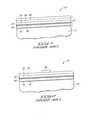
- FIG. 1illustrates a semiconductive wafer fragment 10 at a preliminary step of a prior art gate structure patterning process.
- Semiconductive wafer fragment 10comprises a substrate 12 having a stack 14 of materials formed thereover.
- Substrate 12can comprise, for example, monocrystalline silicon lightly doped with a p-type background dopant.
- the term “semiconductive substrate”is defined to mean any construction comprising semiconductive material, including, but not limited to, bulk semiconductive materials such as a semiconductive wafer (either alone or in assemblies comprising other materials thereon), and semiconductive material layers (either alone or in assemblies comprising other materials).
- substraterefers to any supporting structure, including, but not limited to, the semiconductive substrates described above.
- Stack 14comprises a gate oxide layer 16 , a polysilicon layer 18 , a metal silicide layer 20 , an oxide layer 22 , a nitride layer 24 , an antireflective material layer 26 , and a photoresist layer 28 .
- Gate oxide layer 16can comprise, for example, silicon dioxide, and forms an insulating layer between polysilicon layer 18 and substrate 12 .
- Polysilicon layer 18can comprise, for example, conductively doped polysilicon, and will ultimately be patterned into a first conductive portion of a transistor gate.
- Silicide layer 20comprises a metal silicide, such as, for example, tungsten silicide or titanium silicide, and will ultimately comprise a second conductive portion of a transistor gate.
- a metal silicidesuch as, for example, tungsten silicide or titanium silicide
- the silicidePrior to utilization of silicide layer 20 as a conductive portion of a transistor gate, the silicide is typically subjected to an anneal to improve crystallinity and conductivity of the silicide material of layer 20 .
- Such annealcan comprise, for example, a temperature of from about 800° C. to about 900° C. for a time of about thirty minutes with a nitrogen (N 2 ) purge.
- oxide layer 22is preferably provided over silicide layer 20 prior to the anneal.
- Oxide layer 22can comprise, for example, silicon dioxide.
- Another purpose of having oxide layer 22 over silicide layer 20is as an insulative layer to prevent electrical contact of silicide layer 20 with other conductive layers ultimately formed proximate silicide layer 20 .
- Nitride layer 24can comprise, for example, silicon nitride, and is provided to further electrically insulate conductive layers 18 and 20 from other conductive layers which may ultimately be formed proximate layers 18 and 20 .
- Nitride layer 24is a thick layer (a typical thickness can be on the order of several hundred, or a few thousand Angstroms) and can create stress on underlying layers. Accordingly, another function of oxide layer 22 is to alleviate stress induced by nitride layer 24 on underlying layers 18 and 20 .
- Antireflective material layer 26can comprise, for example, an organic layer that is spun over nitride layer 24 .
- layer 26can be a deposited inorganic antireflective material, such as, for example, Si x O y N z :H, wherein x is from 0.39 to 0.65, y is from 0.02 to 0.56, and z is from 0.05 to 0.33.
- the layercan be substantially inorganic, with the term “substantially inorganic” indicating that the layer can contain a small amount of carbon (less than 1% by weight). Alternatively, if, for example, organic precursors are utilized, the layer can have greater than or equal to 1% carbon, by weight.
- Photoresist layer 28can comprise either a positive or a negative photoresist.
- Photoresist layer 28is patterned by exposing the layer to light through a masked light source.
- the maskcontains clear and opaque features defining a pattern to be created in photoresist layer 28 .
- Regions of photoresist layer 28 which are exposed to lightare made either soluble or insoluble in a solvent. If the exposed regions are soluble, a positive image of the mask is produced in photoresist layer 28 and the resist is termed a positive photoresist.
- the photoresistis referred to as a negative photoresist.
- a difficulty that can occur when exposing photoresist layer 28 to radiationis that waves of the radiation can propagate through photoresist 28 to a layer beneath the photoresist and then be reflected back up through the photoresist to interact with other waves of the radiation which are propagating through the photoresist.
- the reflected wavescan constructively and/or destructively interfere with the other waves to create periodic variations of light intensity within the photoresist.
- Such variations of light intensitycan cause the photoresist to receive non-uniform doses of energy throughout its thickness.
- the non-uniform dosescan decrease the accuracy and precision with which a masked pattern is transferred to the photoresist.
- Antireflective material 26is provided to suppress waves from reflecting back into photoresist layer 28 .
- Antireflective layer 26comprises materials which absorb and/or attenuate radiation and which therefore reduce or eliminate reflection of the radiation.
- FIG. 2shows semiconductive wafer fragment 10 after photoresist layer 28 is patterned by exposure to light and solvent to remove portions of layer 28 .
- a pattern from layer 28is transferred to underlying layers 16 , 18 , 20 , 22 , 24 , and 26 to form a patterned stack 30 .
- Such transfer of a pattern from masking layer 28can occur by a suitable etch, such as, for example, a plasma etch utilizing one or more of Cl, HBr, CF 4 , CH 2 F 2 , He, and NF 3 .
- layers 28 and 26can be removed to leave a patterned gate stack comprising layers 16 , 18 , 20 , 22 , and 24 .
- a continuing goal in semiconductor wafer fabrication technologiesis to reduce process complexity. Such reduction can comprise, for example, reducing a number of process steps, or reducing a number of layers utilized in forming a particular semiconductor structure. Accordingly, it would be desirable to develop alternative methods of forming patterned gate stacks wherein fewer steps and/or layers are utilized than those utilized in the prior art embodiment described with reference to FIGS. 1 - 3 .
- the inventionencompasses a semiconductor processing method.
- a metal silicide layeris formed over a substrate.
- An antireflective material layeris chemical vapor deposited in physical contact with the metal silicide layer.
- a layer of photoresistis applied over the antireflective material layer and patterned photolithographically.
- the inventionencompasses a gate stack forming method.
- a polysilicon layeris formed over a substrate.
- a metal silicide layeris formed over the polysilicon layer.
- An antireflective material layeris deposited over the metal silicide layer.
- a silicon nitride layeris formed over the antireflective material layer and a layer of photoresist is formed over the silicon nitride layer.
- the layer of photoresistis photolithographically patterned to form a masking layer from the layer of photoresist.
- a patternis transferred from the masking layer to the silicon nitride layer, antireflective material layer, metal silicide layer and polysilicon layer to pattern the silicon nitride layer, antireflective material layer, metal silicide layer and polysilicon layer into a gate stack.
- the inventionencompasses a gate stack comprising a polysilicon layer over a semiconductive substrate.
- the gate stackfurther comprises a metal silicide layer over the polysilicon layer, and a layer comprising silicon, oxygen and nitrogen over the metal silicide.
- the gate stackcomprises a silicon nitride layer over the layer comprising silicon, oxygen and nitrogen.
- FIG. 1is a fragmentary, diagrammatic, cross-sectional view of a semiconductive wafer fragment at a preliminary processing step of a prior art process.
- FIG. 2is a view of the FIG. 1 wafer fragment at a prior art processing step subsequent to that of FIG. 1.
- FIG. 3is a view of the FIG. 1 wafer fragment at a prior art processing step subsequent to that of FIG. 2.
- FIG. 4is a fragmentary, diagrammatic, cross-sectional view of a semiconductive wafer fragment at a preliminary processing step of a method of the present invention.
- FIG. 5is a view of the FIG. 4 wafer fragment at a processing step subsequent to that of FIG. 4.
- FIG. 6is a view of the FIG. 4 wafer fragment at a processing step subsequent to that of FIG. 5.
- FIGS. 4 - 6An embodiment encompassed by the present invention is described with reference to FIGS. 4 - 6 .
- similar numbering to that utilized above in describing the prior art processing of FIGS. 1 - 3will be used, with differences indicated by the suffix “a”, or by different numerals.
- Wafer fragment 10 ais illustrated at a preliminary processing step.
- Wafer fragment 10 alike the wafer fragment 10 of FIGS. 1 - 3 , comprises a substrate 12 , a gate oxide layer 16 , a polysilicon layer 18 , and a silicide layer 20 .
- a layer 50comprising silicon, nitrogen, and oxygen is formed over silicide 20 , and in the shown preferred embodiment is formed in physical contact with silicide layer 20 .
- Layer 50thus replaces the oxide layer 22 of the prior art embodiment of FIGS. 1 - 3 .
- Layer 50is preferably formed by chemical vapor deposition (CVD).
- Layer 50can be formed by, for example, CVD utilizing SiH 4 and N 2 O as precursors, in a reaction chamber at a temperature of about 400° C. Such deposition can be performed either with or without a plasma being present within the reaction chamber.
- CVDchemical vapor deposition
- Exemplary conditions for depositing layer 50include flowing SiH 4 into a plasma-enhanced CVD chamber at a rate of from about 40 standard cubic centimeters per minute (SCCM) to about 300 SCCM (preferably about 80 SCCM), N 2 O at a rate of from about 80 SCCM to about 600 SCCM (preferably about 80 SCCM), He at a rate from about 1300 SCCM to about 2500 SCCM (preferably about 2200 SCCM), with a pressure within the chamber of from about 4 Torr to about 6.5 Torr, and a power to the chamber of from about 50 watts to about 200 watts (preferably about 100 watts).
- SCCMstandard cubic centimeters per minute
- N 2 Oat a rate of from about 80 SCCM to about 600 SCCM (preferably about 80 SCCM)
- Heat a rate from about 1300 SCCM to about 2500 SCCM (preferably about 2200 SCCM)
- a pressure within the chamberof from about 4 Torr to about 6.5 Torr
- a power to the chamberof from about 50
- the above-described exemplary conditionscan further include flowing nitrogen gas (N 2 ) into the reaction chamber at a rate of from greater than 0 SCCM to about 300 SCCM, and preferably at a rate of about 200 SCCM, and/or flowing NH 3 into the reaction chamber at a rate of from greater than 0 SCCM to about 100 SCCM.
- N 2nitrogen gas
- the relative values of x, y, z and the hydrogen contentcan be adjusted to alter absorbance characteristics of the deposited material.
- Layer 50preferably has a thickness of from about 250 ⁇ to about 650 ⁇ .
- Layer 50is preferably provided over silicide layer 20 before annealing layer 20 .
- Layer 50thus provides the above-described function of oxide layer 22 (described with reference to FIGS. 1 - 3 ) of protecting silicide layer 20 from exposure to gaseous oxygen during annealing of the silicide layer.
- a silicon nitride layer 24is formed over layer 50 , and can be in physical contact with layer 50 .
- silicon nitride layer 24can exert stress on underlying layers.
- layer 50can serve a function of prior art silicon dioxide layer 22 (discussed with reference to FIGS. 1 - 3 ) of alleviating such stress from adversely impacting underlying conductive layers 20 and 18 .
- Silicon nitride layer 24can be formed over layer 50 either before or after annealing silicide layer 20 .
- a photoresist layer 28is formed over silicon nitride layer 24 .
- layer 50is preferably utilized to serve the function of an antireflective material.
- nitride layer 24is effectively transparent to radiation utilized in patterning photoresist layer 28 . Accordingly, radiation which penetrates photoresist layer 28 will generally also penetrate silicon nitride layer 24 and thereafter enter layer 50 .
- the stoichiometry of silicon, oxygen and nitrogen of layer 50is appropriately adjusted to cancel radiation reaching layer 50 from being reflected back into photoresist layer 28 .
- Such adjustment of stoichiometrycan be adjusted with routine experimentation utilizing methods known to persons of ordinary skill in the art.
- Another way of describing the adjustment of layers 24 and 50is that layers 24 and 50 can be tuned in thickness (by adjusting thickness of one or both of layers 24 and 50 ) and stoichiometry (by adjusting a stoichiometry of layer 50 ) such that reflection back into an overlying layer of photoresist is minimized.
- photoresist layer 28is patterned to form a patterned mask over a stack 60 comprising layers 16 , 18 , 20 , 50 and 24 .
- a pattern from photoresist layer 28is transferred to stack 60 (FIG. 5) to form a patterned gate stack 70 comprising layers 16 , 18 , 20 , 50 and 24 .
- Such transfer of a pattern from layer 28can be accomplished by, for example, a plasma etch utilizing one or more of Cl, HBr, CF 4 , CH 2 F 2 , He and NF 3 .
- Photoresist layer 28can then be removed from over gate stack 70 . Subsequently, source and drain regions can be implanted adjacent the gate stack, and sidewall spacers can be provided over sidewalls of the gate stack to complete construction of a transistor gate from gate stack 70 .
- the method of the present inventioncan reduce complexity relative to the prior art gate stack forming method described above with reference to FIGS. 1 - 3 .
- the method of the present inventioncan utilize a single layer ( 50 ) to accomplish the various functions of protecting silicide during annealing, reducing stress from an overlying silicon nitride layer, and alleviating reflections of light during photolithographic processing of an overlying photoresist layer.
- the method of the present inventioncan eliminate an entire layer (antireflective layer 26 of FIGS. 1 - 3 ) relative to the prior art process described with reference to FIGS. 1 - 3 .
- Such elimination of a layeralso eliminates fabrication steps associated with forming and removing the layer. Accordingly, methods encompassed by the present invention can be more efficient semiconductor fabrication processes then prior art methods.
Landscapes
- Engineering & Computer Science (AREA)
- Condensed Matter Physics & Semiconductors (AREA)
- General Physics & Mathematics (AREA)
- Manufacturing & Machinery (AREA)
- Computer Hardware Design (AREA)
- Microelectronics & Electronic Packaging (AREA)
- Power Engineering (AREA)
- Physics & Mathematics (AREA)
- Insulated Gate Type Field-Effect Transistor (AREA)
- Electrodes Of Semiconductors (AREA)
- Internal Circuitry In Semiconductor Integrated Circuit Devices (AREA)
- Formation Of Insulating Films (AREA)
- Exposure Of Semiconductors, Excluding Electron Or Ion Beam Exposure (AREA)
- Semiconductor Memories (AREA)
- Semiconductor Integrated Circuits (AREA)
- Junction Field-Effect Transistors (AREA)
Abstract
Description
- The invention pertains to methods of forming and utilizing antireflective materials. The invention also pertains to semiconductor processing methods of forming stacks of materials, such as, for example, gate stacks.[0001]
- Semiconductor processing methods frequently involve patterning layers of materials to form a transistor gate structure. FIG. 1 illustrates a[0002]
semiconductive wafer fragment 10 at a preliminary step of a prior art gate structure patterning process.Semiconductive wafer fragment 10 comprises asubstrate 12 having astack 14 of materials formed thereover.Substrate 12 can comprise, for example, monocrystalline silicon lightly doped with a p-type background dopant. To aid in interpretation of the claims that follow, the term “semiconductive substrate” is defined to mean any construction comprising semiconductive material, including, but not limited to, bulk semiconductive materials such as a semiconductive wafer (either alone or in assemblies comprising other materials thereon), and semiconductive material layers (either alone or in assemblies comprising other materials). The term “substrate” refers to any supporting structure, including, but not limited to, the semiconductive substrates described above. - [0003]
Stack 14 comprises agate oxide layer 16, apolysilicon layer 18, ametal silicide layer 20, anoxide layer 22, anitride layer 24, anantireflective material layer 26, and aphotoresist layer 28.Gate oxide layer 16 can comprise, for example, silicon dioxide, and forms an insulating layer betweenpolysilicon layer 18 andsubstrate 12.Polysilicon layer 18 can comprise, for example, conductively doped polysilicon, and will ultimately be patterned into a first conductive portion of a transistor gate. - [0004]
Silicide layer 20 comprises a metal silicide, such as, for example, tungsten silicide or titanium silicide, and will ultimately comprise a second conductive portion of a transistor gate. Prior to utilization ofsilicide layer 20 as a conductive portion of a transistor gate, the silicide is typically subjected to an anneal to improve crystallinity and conductivity of the silicide material oflayer 20. Such anneal can comprise, for example, a temperature of from about 800° C. to about 900° C. for a time of about thirty minutes with a nitrogen (N2) purge. - If[0005]
silicide layer 20 is exposed to gaseous forms of oxygen during the anneal, the silicide layer can become oxidized, which can adversely effect conductivity of the layer. Accordingly,oxide layer 22 is preferably provided oversilicide layer 20 prior to the anneal.Oxide layer 22 can comprise, for example, silicon dioxide. Another purpose of havingoxide layer 22 oversilicide layer 20 is as an insulative layer to prevent electrical contact ofsilicide layer 20 with other conductive layers ultimately formedproximate silicide layer 20. - [0006]
Nitride layer 24 can comprise, for example, silicon nitride, and is provided to further electrically insulateconductive layers proximate layers layer 24 is a thick layer (a typical thickness can be on the order of several hundred, or a few thousand Angstroms) and can create stress on underlying layers. Accordingly, another function ofoxide layer 22 is to alleviate stress induced bynitride layer 24 onunderlying layers - [0007]
Antireflective material layer 26 can comprise, for example, an organic layer that is spun overnitride layer 24. Alternatively,layer 26 can be a deposited inorganic antireflective material, such as, for example, SixOyNz:H, wherein x is from 0.39 to 0.65, y is from 0.02 to 0.56, and z is from 0.05 to 0.33. In practice the layer can be substantially inorganic, with the term “substantially inorganic” indicating that the layer can contain a small amount of carbon (less than 1% by weight). Alternatively, if, for example, organic precursors are utilized, the layer can have greater than or equal to 1% carbon, by weight. - [0008]
Photoresist layer 28 can comprise either a positive or a negative photoresist.Photoresist layer 28 is patterned by exposing the layer to light through a masked light source. The mask contains clear and opaque features defining a pattern to be created inphotoresist layer 28. Regions ofphotoresist layer 28 which are exposed to light are made either soluble or insoluble in a solvent. If the exposed regions are soluble, a positive image of the mask is produced inphotoresist layer 28 and the resist is termed a positive photoresist. On the other hand, if the non-radiated regions are dissolved by the solvent, a negative image results, and the photoresist is referred to as a negative photoresist. - A difficulty that can occur when exposing[0009]
photoresist layer 28 to radiation is that waves of the radiation can propagate throughphotoresist 28 to a layer beneath the photoresist and then be reflected back up through the photoresist to interact with other waves of the radiation which are propagating through the photoresist. The reflected waves can constructively and/or destructively interfere with the other waves to create periodic variations of light intensity within the photoresist. Such variations of light intensity can cause the photoresist to receive non-uniform doses of energy throughout its thickness. The non-uniform doses can decrease the accuracy and precision with which a masked pattern is transferred to the photoresist.Antireflective material 26 is provided to suppress waves from reflecting back intophotoresist layer 28.Antireflective layer 26 comprises materials which absorb and/or attenuate radiation and which therefore reduce or eliminate reflection of the radiation. - FIG. 2 shows[0010]
semiconductive wafer fragment 10 afterphotoresist layer 28 is patterned by exposure to light and solvent to remove portions oflayer 28. - Referring to FIG. 3, a pattern from[0011]
layer 28 is transferred to underlyinglayers stack 30. Such transfer of a pattern frommasking layer 28 can occur by a suitable etch, such as, for example, a plasma etch utilizing one or more of Cl, HBr, CF4, CH2F2, He, and NF3. - After the patterning of[0012]
layers layers stack comprising layers - A continuing goal in semiconductor wafer fabrication technologies is to reduce process complexity. Such reduction can comprise, for example, reducing a number of process steps, or reducing a number of layers utilized in forming a particular semiconductor structure. Accordingly, it would be desirable to develop alternative methods of forming patterned gate stacks wherein fewer steps and/or layers are utilized than those utilized in the prior art embodiment described with reference to FIGS.[0013]1-3.
- In one aspect, the invention encompasses a semiconductor processing method. A metal silicide layer is formed over a substrate. An antireflective material layer is chemical vapor deposited in physical contact with the metal silicide layer. A layer of photoresist is applied over the antireflective material layer and patterned photolithographically.[0014]
- In another aspect, the invention encompasses a gate stack forming method. A polysilicon layer is formed over a substrate. A metal silicide layer is formed over the polysilicon layer. An antireflective material layer is deposited over the metal silicide layer. A silicon nitride layer is formed over the antireflective material layer and a layer of photoresist is formed over the silicon nitride layer. The layer of photoresist is photolithographically patterned to form a masking layer from the layer of photoresist. A pattern is transferred from the masking layer to the silicon nitride layer, antireflective material layer, metal silicide layer and polysilicon layer to pattern the silicon nitride layer, antireflective material layer, metal silicide layer and polysilicon layer into a gate stack.[0015]
- In yet another aspect, the invention encompasses a gate stack comprising a polysilicon layer over a semiconductive substrate. The gate stack further comprises a metal silicide layer over the polysilicon layer, and a layer comprising silicon, oxygen and nitrogen over the metal silicide. Additionally, the gate stack comprises a silicon nitride layer over the layer comprising silicon, oxygen and nitrogen.[0016]
- Preferred embodiments of the invention are described below with reference to the following accompanying drawings.[0017]
- FIG. 1 is a fragmentary, diagrammatic, cross-sectional view of a semiconductive wafer fragment at a preliminary processing step of a prior art process.[0018]
- FIG. 2 is a view of the FIG. 1 wafer fragment at a prior art processing step subsequent to that of FIG. 1.[0019]
- FIG. 3 is a view of the FIG. 1 wafer fragment at a prior art processing step subsequent to that of FIG. 2.[0020]
- FIG. 4 is a fragmentary, diagrammatic, cross-sectional view of a semiconductive wafer fragment at a preliminary processing step of a method of the present invention.[0021]
- FIG. 5 is a view of the FIG. 4 wafer fragment at a processing step subsequent to that of FIG. 4.[0022]
- FIG. 6 is a view of the FIG. 4 wafer fragment at a processing step subsequent to that of FIG. 5.[0023]
- This disclosure of the invention is submitted in furtherance of the constitutional purposes of the U.S. Patent Laws “to promote the progress of science and useful arts” (Article 1, Section 8).[0024]
- An embodiment encompassed by the present invention is described with reference to FIGS.[0025]4-6. In describing the embodiment of FIGS.4-6, similar numbering to that utilized above in describing the prior art processing of FIGS.1-3 will be used, with differences indicated by the suffix “a”, or by different numerals.
- Referring to FIG. 4, a semiconductive wafer fragment[0026]10ais illustrated at a preliminary processing step. Wafer fragment10a, like the
wafer fragment 10 of FIGS.1-3, comprises asubstrate 12, agate oxide layer 16, apolysilicon layer 18, and asilicide layer 20. However, in contrast to the prior art processing described above with reference to FIGS.1-3, alayer 50 comprising silicon, nitrogen, and oxygen is formed oversilicide 20, and in the shown preferred embodiment is formed in physical contact withsilicide layer 20.Layer 50 thus replaces theoxide layer 22 of the prior art embodiment of FIGS.1-3. - [0027]
Layer 50 is preferably formed by chemical vapor deposition (CVD).Layer 50 can be formed by, for example, CVD utilizing SiH4and N2O as precursors, in a reaction chamber at a temperature of about 400° C. Such deposition can be performed either with or without a plasma being present within the reaction chamber. Exemplary conditions for depositinglayer 50 include flowing SiH4into a plasma-enhanced CVD chamber at a rate of from about 40 standard cubic centimeters per minute (SCCM) to about 300 SCCM (preferably about 80 SCCM), N2O at a rate of from about 80 SCCM to about 600 SCCM (preferably about 80 SCCM), He at a rate from about 1300 SCCM to about 2500 SCCM (preferably about 2200 SCCM), with a pressure within the chamber of from about 4 Torr to about 6.5 Torr, and a power to the chamber of from about 50 watts to about 200 watts (preferably about 100 watts). - The above-described exemplary conditions can further include flowing nitrogen gas (N[0028]2) into the reaction chamber at a rate of from greater than 0 SCCM to about 300 SCCM, and preferably at a rate of about 200 SCCM, and/or flowing NH3into the reaction chamber at a rate of from greater than 0 SCCM to about 100 SCCM.
- An exemplary composition of[0029]
layer 50 is SixNyOz:H, wherein x=0.5, y=0.37, and z=0.13. The relative values of x, y, z and the hydrogen content can be adjusted to alter absorbance characteristics of the deposited material.Layer 50 preferably has a thickness of from about 250 Å to about 650 Å. - [0030]
Layer 50 is preferably provided oversilicide layer 20 before annealinglayer 20.Layer 50 thus provides the above-described function of oxide layer22 (described with reference to FIGS.1-3) of protectingsilicide layer 20 from exposure to gaseous oxygen during annealing of the silicide layer. - A[0031]
silicon nitride layer 24 is formed overlayer 50, and can be in physical contact withlayer 50. As discussed above in the background section of this disclosure,silicon nitride layer 24 can exert stress on underlying layers. Accordingly,layer 50 can serve a function of prior art silicon dioxide layer22 (discussed with reference to FIGS.1-3) of alleviating such stress from adversely impacting underlyingconductive layers Silicon nitride layer 24 can be formed overlayer 50 either before or after annealingsilicide layer 20. - A[0032]
photoresist layer 28 is formed oversilicon nitride layer 24. In contrast to the prior art embodiment discussed with reference to FIGS.1-3, there is no antireflective material layer formed betweensilicon nitride layer 24 andphotoresist layer 28. Instead,layer 50 is preferably utilized to serve the function of an antireflective material. Specifically,nitride layer 24 is effectively transparent to radiation utilized inpatterning photoresist layer 28. Accordingly, radiation which penetratesphotoresist layer 28 will generally also penetratesilicon nitride layer 24 and thereafter enterlayer 50. Preferably, the stoichiometry of silicon, oxygen and nitrogen oflayer 50 is appropriately adjusted to cancelradiation reaching layer 50 from being reflected back intophotoresist layer 28. Such adjustment of stoichiometry can be adjusted with routine experimentation utilizing methods known to persons of ordinary skill in the art. Another way of describing the adjustment oflayers layers 24 and50) and stoichiometry (by adjusting a stoichiometry of layer50) such that reflection back into an overlying layer of photoresist is minimized. - Referring to FIG. 5,[0033]
photoresist layer 28 is patterned to form a patterned mask over astack 60 comprisinglayers - Referring to FIG. 6, a pattern from[0034]
photoresist layer 28 is transferred to stack60 (FIG. 5) to form apatterned gate stack 70 comprisinglayers layer 28 can be accomplished by, for example, a plasma etch utilizing one or more of Cl, HBr, CF4, CH2F2, He and NF3.Photoresist layer 28 can then be removed from overgate stack 70. Subsequently, source and drain regions can be implanted adjacent the gate stack, and sidewall spacers can be provided over sidewalls of the gate stack to complete construction of a transistor gate fromgate stack 70. - The method of the present invention can reduce complexity relative to the prior art gate stack forming method described above with reference to FIGS.[0035]1-3. Specifically, the method of the present invention can utilize a single layer (50) to accomplish the various functions of protecting silicide during annealing, reducing stress from an overlying silicon nitride layer, and alleviating reflections of light during photolithographic processing of an overlying photoresist layer. Accordingly, the method of the present invention can eliminate an entire layer (
antireflective layer 26 of FIGS.1-3) relative to the prior art process described with reference to FIGS.1-3. Such elimination of a layer also eliminates fabrication steps associated with forming and removing the layer. Accordingly, methods encompassed by the present invention can be more efficient semiconductor fabrication processes then prior art methods. - In compliance with the statute, the invention has been described in language more or less specific as to structural and methodical features. It is to be understood, however, that the invention is not limited to the specific features shown and described, since the means herein disclosed comprise preferred forms of putting the invention into effect. The invention is, therefore, claimed in any of its forms or modifications within the proper scope of the appended claims appropriately interpreted in accordance with the doctrine of equivalents.[0036]
Claims (31)
Priority Applications (1)
| Application Number | Priority Date | Filing Date | Title |
|---|---|---|---|
| US09/870,850US6461950B2 (en) | 1998-09-03 | 2001-05-30 | Semiconductor processing methods, semiconductor circuitry, and gate stacks |
Applications Claiming Priority (2)
| Application Number | Priority Date | Filing Date | Title |
|---|---|---|---|
| US09/146,842US6281100B1 (en) | 1998-09-03 | 1998-09-03 | Semiconductor processing methods |
| US09/870,850US6461950B2 (en) | 1998-09-03 | 2001-05-30 | Semiconductor processing methods, semiconductor circuitry, and gate stacks |
Related Parent Applications (1)
| Application Number | Title | Priority Date | Filing Date |
|---|---|---|---|
| US09/146,842ContinuationUS6281100B1 (en) | 1998-09-03 | 1998-09-03 | Semiconductor processing methods |
Publications (2)
| Publication Number | Publication Date |
|---|---|
| US20010028095A1true US20010028095A1 (en) | 2001-10-11 |
| US6461950B2 US6461950B2 (en) | 2002-10-08 |
Family
ID=22519209
Family Applications (4)
| Application Number | Title | Priority Date | Filing Date |
|---|---|---|---|
| US09/146,842Expired - LifetimeUS6281100B1 (en) | 1998-09-03 | 1998-09-03 | Semiconductor processing methods |
| US09/559,903Expired - Fee RelatedUS7576400B1 (en) | 1998-09-03 | 2000-04-26 | Circuitry and gate stacks |
| US09/870,850Expired - LifetimeUS6461950B2 (en) | 1998-09-03 | 2001-05-30 | Semiconductor processing methods, semiconductor circuitry, and gate stacks |
| US12/537,577AbandonedUS20090294878A1 (en) | 1998-09-03 | 2009-08-07 | Circuitry and gate stacks |
Family Applications Before (2)
| Application Number | Title | Priority Date | Filing Date |
|---|---|---|---|
| US09/146,842Expired - LifetimeUS6281100B1 (en) | 1998-09-03 | 1998-09-03 | Semiconductor processing methods |
| US09/559,903Expired - Fee RelatedUS7576400B1 (en) | 1998-09-03 | 2000-04-26 | Circuitry and gate stacks |
Family Applications After (1)
| Application Number | Title | Priority Date | Filing Date |
|---|---|---|---|
| US12/537,577AbandonedUS20090294878A1 (en) | 1998-09-03 | 2009-08-07 | Circuitry and gate stacks |
Country Status (8)
| Country | Link |
|---|---|
| US (4) | US6281100B1 (en) |
| EP (1) | EP1114444B1 (en) |
| JP (1) | JP2003506854A (en) |
| KR (1) | KR100434560B1 (en) |
| AT (1) | ATE345580T1 (en) |
| AU (1) | AU5590699A (en) |
| DE (1) | DE69934019T2 (en) |
| WO (1) | WO2000014780A1 (en) |
Cited By (3)
| Publication number | Priority date | Publication date | Assignee | Title |
|---|---|---|---|---|
| US6798065B2 (en)* | 1999-03-24 | 2004-09-28 | Newport Fab, Llc | Method and apparatus for high-resolution in-situ plasma etching of inorganic and metals films |
| US20190229212A1 (en)* | 2018-01-19 | 2019-07-25 | Silergy Semiconductor Technology (Hangzhou) Ltd | LDMOS Transistor And Method For Manufacturing The Same |
| US20220130981A1 (en)* | 2020-10-23 | 2022-04-28 | Hangzhou Silicon-Magic Semiconductor Technology Co., Ltd. | Ldmos transistor and manufacturing method thereof |
Families Citing this family (24)
| Publication number | Priority date | Publication date | Assignee | Title |
|---|---|---|---|---|
| US6274292B1 (en)* | 1998-02-25 | 2001-08-14 | Micron Technology, Inc. | Semiconductor processing methods |
| US7804115B2 (en) | 1998-02-25 | 2010-09-28 | Micron Technology, Inc. | Semiconductor constructions having antireflective portions |
| US6291868B1 (en)* | 1998-02-26 | 2001-09-18 | Micron Technology, Inc. | Forming a conductive structure in a semiconductor device |
| US6268282B1 (en) | 1998-09-03 | 2001-07-31 | Micron Technology, Inc. | Semiconductor processing methods of forming and utilizing antireflective material layers, and methods of forming transistor gate stacks |
| US6828683B2 (en) | 1998-12-23 | 2004-12-07 | Micron Technology, Inc. | Semiconductor devices, and semiconductor processing methods |
| US7235499B1 (en)* | 1999-01-20 | 2007-06-26 | Micron Technology, Inc. | Semiconductor processing methods |
| US7067414B1 (en) | 1999-09-01 | 2006-06-27 | Micron Technology, Inc. | Low k interlevel dielectric layer fabrication methods |
| JP3498022B2 (en)* | 1999-10-15 | 2004-02-16 | Necエレクトロニクス株式会社 | Method for manufacturing semiconductor device |
| US6440860B1 (en) | 2000-01-18 | 2002-08-27 | Micron Technology, Inc. | Semiconductor processing methods of transferring patterns from patterned photoresists to materials, and structures comprising silicon nitride |
| KR100408743B1 (en)* | 2001-09-21 | 2003-12-11 | 삼성전자주식회사 | Method of forming a quantum dot and method of forming a gate electrode using the same |
| US6573175B1 (en)* | 2001-11-30 | 2003-06-03 | Micron Technology, Inc. | Dry low k film application for interlevel dielectric and method of cleaning etched features |
| US6777829B2 (en) | 2002-03-13 | 2004-08-17 | Celis Semiconductor Corporation | Rectifier utilizing a grounded antenna |
| US6720235B2 (en)* | 2002-09-10 | 2004-04-13 | Silicon Integrated System Corp. | Method of forming shallow trench isolation in a semiconductor substrate |
| US7384727B2 (en)* | 2003-06-26 | 2008-06-10 | Micron Technology, Inc. | Semiconductor processing patterning methods |
| US7115532B2 (en) | 2003-09-05 | 2006-10-03 | Micron Technolgoy, Inc. | Methods of forming patterned photoresist layers over semiconductor substrates |
| US7132201B2 (en)* | 2003-09-12 | 2006-11-07 | Micron Technology, Inc. | Transparent amorphous carbon structure in semiconductor devices |
| US7129180B2 (en)* | 2003-09-12 | 2006-10-31 | Micron Technology, Inc. | Masking structure having multiple layers including an amorphous carbon layer |
| US6969677B2 (en)* | 2003-10-20 | 2005-11-29 | Micron Technology, Inc. | Methods of forming conductive metal silicides by reaction of metal with silicon |
| US7026243B2 (en)* | 2003-10-20 | 2006-04-11 | Micron Technology, Inc. | Methods of forming conductive material silicides by reaction of metal with silicon |
| US7153769B2 (en)* | 2004-04-08 | 2006-12-26 | Micron Technology, Inc. | Methods of forming a reaction product and methods of forming a conductive metal silicide by reaction of metal with silicon |
| US7119031B2 (en)* | 2004-06-28 | 2006-10-10 | Micron Technology, Inc. | Methods of forming patterned photoresist layers over semiconductor substrates |
| US7241705B2 (en)* | 2004-09-01 | 2007-07-10 | Micron Technology, Inc. | Methods of forming conductive contacts to source/drain regions and methods of forming local interconnects |
| JP2009071232A (en)* | 2007-09-18 | 2009-04-02 | Elpida Memory Inc | Semiconductor device and manufacturing method thereof |
| KR102458034B1 (en) | 2015-10-16 | 2022-10-25 | 삼성전자주식회사 | Semiconductor package, Method of fabricating the Semiconductor package, And Semiconductor module |
Family Cites Families (210)
| Publication number | Priority date | Publication date | Assignee | Title |
|---|---|---|---|---|
| US2553314A (en) | 1944-07-01 | 1951-05-15 | Gen Electric | Method of rendering materials water repellent |
| US4158717A (en) | 1977-02-14 | 1979-06-19 | Varian Associates, Inc. | Silicon nitride film and method of deposition |
| US4523214A (en) | 1981-07-03 | 1985-06-11 | Fuji Photo Film Co., Ltd. | Solid state image pickup device utilizing microcrystalline and amorphous silicon |
| US4562091A (en) | 1982-12-23 | 1985-12-31 | International Business Machines Corporation | Use of plasma polymerized orgaosilicon films in fabrication of lift-off masks |
| US4444617A (en) | 1983-01-06 | 1984-04-24 | Rockwell International Corporation | Reactive ion etching of molybdenum silicide and N+ polysilicon |
| US4474975A (en) | 1983-05-09 | 1984-10-02 | The United States Of America As Represented By The Administrator Of The National Aeronautics And Space Administration | Process for producing tris (N-methylamino) methylsilane |
| US4600671A (en) | 1983-09-12 | 1986-07-15 | Canon Kabushiki Kaisha | Photoconductive member having light receiving layer of A-(Si-Ge) and N |
| US4702936A (en) | 1984-09-20 | 1987-10-27 | Applied Materials Japan, Inc. | Gas-phase growth process |
| US4552783A (en)* | 1984-11-05 | 1985-11-12 | General Electric Company | Enhancing the selectivity of tungsten deposition on conductor and semiconductor surfaces |
| US4592129A (en) | 1985-04-01 | 1986-06-03 | Motorola, Inc. | Method of making an integral, multiple layer antireflection coating by hydrogen ion implantation |
| JP2635021B2 (en) | 1985-09-26 | 1997-07-30 | 宣夫 御子柴 | Deposition film forming method and apparatus used for the same |
| US4648904A (en) | 1986-02-14 | 1987-03-10 | Scm Corporation | Aqueous systems containing silanes for rendering masonry surfaces water repellant |
| US6087267A (en) | 1986-03-04 | 2000-07-11 | Motorola, Inc. | Process for forming an integrated circuit |
| JPS63184340A (en)* | 1986-09-08 | 1988-07-29 | Nec Corp | semiconductor equipment |
| US4695859A (en) | 1986-10-20 | 1987-09-22 | Energy Conversion Devices, Inc. | Thin film light emitting diode, photonic circuit employing said diode imager employing said circuits |
| US4764247A (en) | 1987-03-18 | 1988-08-16 | Syn Labs, Inc. | Silicon containing resists |
| JPH043699Y2 (en) | 1987-03-30 | 1992-02-05 | ||
| JPS63316476A (en) | 1987-06-18 | 1988-12-23 | Seiko Instr & Electronics Ltd | Semiconductor device and manufacture thereof |
| US4905073A (en)* | 1987-06-22 | 1990-02-27 | At&T Bell Laboratories | Integrated circuit with improved tub tie |
| US4755478A (en) | 1987-08-13 | 1988-07-05 | International Business Machines Corporation | Method of forming metal-strapped polysilicon gate electrode for FET device |
| US4870470A (en) | 1987-10-16 | 1989-09-26 | International Business Machines Corporation | Non-volatile memory cell having Si rich silicon nitride charge trapping layer |
| US4863755A (en) | 1987-10-16 | 1989-09-05 | The Regents Of The University Of California | Plasma enhanced chemical vapor deposition of thin films of silicon nitride from cyclic organosilicon nitrogen precursors |
| US4833096A (en) | 1988-01-19 | 1989-05-23 | Atmel Corporation | EEPROM fabrication process |
| US4805683A (en) | 1988-03-04 | 1989-02-21 | International Business Machines Corporation | Method for producing a plurality of layers of metallurgy |
| US4940509A (en) | 1988-03-25 | 1990-07-10 | Texas Instruments, Incorporated | Isotropic etchant for capped silicide processes |
| JPH02285638A (en) | 1989-04-27 | 1990-11-22 | Toshiba Corp | semiconductor equipment |
| US5270267A (en) | 1989-05-31 | 1993-12-14 | Mitel Corporation | Curing and passivation of spin on glasses by a plasma process wherein an external polarization field is applied to the substrate |
| US4910160A (en) | 1989-06-06 | 1990-03-20 | National Semiconductor Corporation | High voltage complementary NPN/PNP process |
| US5061509A (en) | 1989-08-25 | 1991-10-29 | Kabushiki Kaisha Toshiba | Method of manufacturing polyimide thin film and method of manufacturing liquid crystal orientation film of polyimide |
| US4971655A (en)* | 1989-12-26 | 1990-11-20 | Micron Technology, Inc. | Protection of a refractory metal silicide during high-temperature processing using a dual-layer cap of silicon dioxide and silicon nitride |
| US5244537A (en) | 1989-12-27 | 1993-09-14 | Honeywell, Inc. | Fabrication of an electronic microvalve apparatus |
| US4992306A (en) | 1990-02-01 | 1991-02-12 | Air Products Abd Chemicals, Inc. | Deposition of silicon dioxide and silicon oxynitride films using azidosilane sources |
| US5140390A (en) | 1990-02-16 | 1992-08-18 | Hughes Aircraft Company | High speed silicon-on-insulator device |
| JP2814009B2 (en) | 1990-06-05 | 1998-10-22 | 三菱電機株式会社 | Method for manufacturing semiconductor device |
| US5219613A (en) | 1990-06-13 | 1993-06-15 | Wacker-Chemitronic Gesellschaft Fur Elektronik-Grundstoffe Mbh | Process for producing storage-stable surfaces of polished silicon wafers |
| JP2637265B2 (en) | 1990-06-28 | 1997-08-06 | 株式会社東芝 | Method of forming silicon nitride film |
| US5034348A (en) | 1990-08-16 | 1991-07-23 | International Business Machines Corp. | Process for forming refractory metal silicide layers of different thicknesses in an integrated circuit |
| US5356515A (en) | 1990-10-19 | 1994-10-18 | Tokyo Electron Limited | Dry etching method |
| WO1992012535A1 (en) | 1991-01-08 | 1992-07-23 | Fujitsu Limited | Process for forming silicon oxide film |
| US5302366A (en) | 1991-03-28 | 1994-04-12 | Phillips Petroleum Company | Production of silicon product containing both carbon and nitrogen |
| CA2056456C (en) | 1991-08-14 | 2001-05-08 | Luc Ouellet | High performance passivation for semiconductor devices |
| US5652187A (en) | 1991-10-30 | 1997-07-29 | Samsung Electronics Co., Ltd. | Method for fabricating doped interlayer-dielectric film of semiconductor device using a plasma treatment |
| KR940009599B1 (en) | 1991-10-30 | 1994-10-15 | 삼성전자 주식회사 | Forming method of inter-dielectric film for semiconductor device |
| US5470772A (en) | 1991-11-06 | 1995-11-28 | Intel Corporation | Silicidation method for contactless EPROM related devices |
| US5677111A (en) | 1991-12-20 | 1997-10-14 | Sony Corporation | Process for production of micropattern utilizing antireflection film |
| US5472829A (en) | 1991-12-30 | 1995-12-05 | Sony Corporation | Method of forming a resist pattern by using an anti-reflective layer |
| US5670297A (en) | 1991-12-30 | 1997-09-23 | Sony Corporation | Process for the formation of a metal pattern |
| US5472827A (en) | 1991-12-30 | 1995-12-05 | Sony Corporation | Method of forming a resist pattern using an anti-reflective layer |
| JPH0667019A (en) | 1992-01-17 | 1994-03-11 | Asahi Glass Co Ltd | Antireflection layer and its production |
| US5543654A (en) | 1992-01-28 | 1996-08-06 | Thunderbird Technologies, Inc. | Contoured-tub fermi-threshold field effect transistor and method of forming same |
| US5653619A (en) | 1992-03-02 | 1997-08-05 | Micron Technology, Inc. | Method to form self-aligned gate structures and focus rings |
| JPH05263255A (en) | 1992-03-19 | 1993-10-12 | Hitachi Electron Eng Co Ltd | Plasma cvd device |
| JPH05275345A (en) | 1992-03-30 | 1993-10-22 | Nippon Sheet Glass Co Ltd | Plasma cvd method and its device |
| EP0572704B1 (en) | 1992-06-05 | 2000-04-19 | Semiconductor Process Laboratory Co., Ltd. | Method for manufacturing a semiconductor device including method of reforming an insulating film formed by low temperature CVD |
| EP0731982B1 (en) | 1992-07-04 | 1999-12-01 | Trikon Equipments Limited | A method of treating a semiconductor wafer |
| TW363146B (en) | 1992-08-20 | 1999-07-01 | Sony Corp | An anti-reflective layer and a method of forming a photoresist pattern |
| US5286661A (en) | 1992-08-26 | 1994-02-15 | Motorola, Inc. | Method of forming a bipolar transistor having an emitter overhang |
| DE4231312C2 (en) | 1992-09-18 | 1996-10-02 | Siemens Ag | Anti-reflective layer and method for the lithographic structuring of a layer |
| JP2684942B2 (en) | 1992-11-30 | 1997-12-03 | 日本電気株式会社 | Chemical vapor deposition method, chemical vapor deposition apparatus, and method for manufacturing multilayer wiring |
| US5429987A (en) | 1993-01-25 | 1995-07-04 | Sharp Microelectronics Technology, Inc. | Method for profile control of selective metallization |
| JPH06244172A (en) | 1993-02-18 | 1994-09-02 | Toray Ind Inc | Multilayered wiring structure |
| US5312768A (en) | 1993-03-09 | 1994-05-17 | Micron Technology, Inc. | Integrated process for fabricating raised, source/drain, short-channel transistors |
| US5397684A (en) | 1993-04-27 | 1995-03-14 | International Business Machines Corporation | Antireflective polyimide dielectric for photolithography |
| US5378659A (en) | 1993-07-06 | 1995-01-03 | Motorola Inc. | Method and structure for forming an integrated circuit pattern on a semiconductor substrate |
| KR970004447B1 (en) | 1993-09-08 | 1997-03-27 | 삼성전자 주식회사 | A method for forming anti-reflect-film and its application to manufacturing semiconductor devices |
| KR970007116B1 (en) | 1993-08-31 | 1997-05-02 | 삼성전자 주식회사 | Method for forming insulating layer of semiconductor device and apparatus for forming same |
| JP2641385B2 (en) | 1993-09-24 | 1997-08-13 | アプライド マテリアルズ インコーポレイテッド | Film formation method |
| FR2711275B1 (en)* | 1993-10-15 | 1996-10-31 | Intel Corp | Automatically aligned contact process in semiconductor and product device manufacturing. |
| JP3326943B2 (en) | 1993-12-29 | 2002-09-24 | ソニー株式会社 | Semiconductor device manufacturing method and semiconductor device |
| JP3029235B2 (en) | 1993-12-29 | 2000-04-04 | 現代電子産業株式会社 | Method for forming charge storage electrode of semiconductor device |
| US5508881A (en)* | 1994-02-01 | 1996-04-16 | Quality Microcircuits Corporation | Capacitors and interconnect lines for use with integrated circuits |
| US5677015A (en) | 1994-03-17 | 1997-10-14 | Sony Corporation | High dielectric constant material containing tantalum, process for forming high dielectric constant film containing tantalum, and semiconductor device using the same |
| JP3254885B2 (en) | 1994-03-22 | 2002-02-12 | 双葉電子工業株式会社 | Manufacturing method of resistor |
| KR100366910B1 (en) | 1994-04-05 | 2003-03-04 | 소니 가부시끼 가이샤 | Manufacturing method of semiconductor device |
| US5441914A (en) | 1994-05-02 | 1995-08-15 | Motorola Inc. | Method of forming conductive interconnect structure |
| US5858880A (en) | 1994-05-14 | 1999-01-12 | Trikon Equipment Limited | Method of treating a semi-conductor wafer |
| US5461003A (en) | 1994-05-27 | 1995-10-24 | Texas Instruments Incorporated | Multilevel interconnect structure with air gaps formed between metal leads |
| CN1274009C (en) | 1994-06-15 | 2006-09-06 | 精工爱普生株式会社 | Method for making thin-film semicondcutor device |
| US5536857A (en) | 1994-07-05 | 1996-07-16 | Ford Motor Company | Single source volatile precursor for SiO2.TiO2 powders and films |
| JPH0845926A (en)* | 1994-07-26 | 1996-02-16 | Sony Corp | Semiconductor device and its manufacture |
| KR960005761A (en) | 1994-07-27 | 1996-02-23 | 이데이 노부유끼 | Semiconductor device |
| JPH0846186A (en) | 1994-07-27 | 1996-02-16 | Sony Corp | Semiconductor device |
| US5413963A (en) | 1994-08-12 | 1995-05-09 | United Microelectronics Corporation | Method for depositing an insulating interlayer in a semiconductor metallurgy system |
| US5482894A (en)* | 1994-08-23 | 1996-01-09 | Texas Instruments Incorporated | Method of fabricating a self-aligned contact using organic dielectric materials |
| JP3963961B2 (en) | 1994-08-31 | 2007-08-22 | 株式会社半導体エネルギー研究所 | Method for manufacturing semiconductor device |
| US5554567A (en) | 1994-09-01 | 1996-09-10 | Taiwan Semiconductor Manufacturing Company Ltd. | Method for improving adhesion to a spin-on-glass |
| US5439838A (en) | 1994-09-14 | 1995-08-08 | United Microelectronics Corporation | Method of thinning for EEPROM tunneling oxide device |
| US5600153A (en) | 1994-10-07 | 1997-02-04 | Micron Technology, Inc. | Conductive polysilicon lines and thin film transistors |
| JP3334370B2 (en)* | 1994-10-13 | 2002-10-15 | ヤマハ株式会社 | Semiconductor devices |
| US5498555A (en) | 1994-11-07 | 1996-03-12 | United Microelectronics Corporation | Method of making LDD with polysilicon and dielectric spacers |
| US5780891A (en) | 1994-12-05 | 1998-07-14 | Micron Technology, Inc. | Nonvolatile floating gate memory with improved interploy dielectric |
| DE19500674A1 (en) | 1995-01-12 | 1996-07-18 | Degussa | Surface modified pyrogenic mixed oxides, process for their production and use |
| NO303649B1 (en) | 1995-02-03 | 1998-08-10 | Bj Services As | The bridge plug |
| JP3348263B2 (en) | 1995-02-08 | 2002-11-20 | 富士通株式会社 | Method for manufacturing semiconductor device |
| JPH08239241A (en) | 1995-02-28 | 1996-09-17 | Toray Dow Corning Silicone Co Ltd | Water-repelling agent for glass and water-repelling glass |
| US5962581A (en) | 1995-04-28 | 1999-10-05 | Kabushiki Kaisha Toshiba | Silicone polymer composition, method of forming a pattern and method of forming an insulating film |
| FR2734402B1 (en) | 1995-05-15 | 1997-07-18 | Brouquet Pierre | PROCESS FOR ELECTRICAL ISOLATION IN MICROELECTRONICS, APPLICABLE TO NARROW CAVITIES, BY DEPOSITION OF OXIDE IN THE VISCOUS STATE AND CORRESPONDING DEVICE |
| US6040619A (en)* | 1995-06-07 | 2000-03-21 | Advanced Micro Devices | Semiconductor device including antireflective etch stop layer |
| US5710067A (en) | 1995-06-07 | 1998-01-20 | Advanced Micro Devices, Inc. | Silicon oxime film |
| JPH0950993A (en) | 1995-08-08 | 1997-02-18 | Fujitsu Ltd | Insulating film forming method and semiconductor device |
| JPH0955351A (en) | 1995-08-15 | 1997-02-25 | Sony Corp | Manufacture of semiconductor device |
| JP3061255B2 (en) | 1995-08-18 | 2000-07-10 | キヤノン販売株式会社 | Film formation method |
| JPH0982687A (en) | 1995-09-19 | 1997-03-28 | Mitsubishi Electric Corp | Method for manufacturing semiconductor device |
| US5948482A (en) | 1995-09-19 | 1999-09-07 | University Of New Mexico | Ambient pressure process for preparing aerogel thin films reliquified sols useful in preparing aerogel thin films |
| US5750442A (en) | 1995-09-25 | 1998-05-12 | Micron Technology, Inc. | Germanium as an antireflective coating and method of use |
| TW362118B (en) | 1995-10-30 | 1999-06-21 | Dow Corning | Method for depositing amorphous SiNC coatings |
| US5744399A (en) | 1995-11-13 | 1998-04-28 | Lsi Logic Corporation | Process for forming low dielectric constant layers using fullerenes |
| US5926739A (en) | 1995-12-04 | 1999-07-20 | Micron Technology, Inc. | Semiconductor processing method of promoting photoresist adhesion to an outer substrate layer predominately comprising silicon nitride |
| US5968324A (en) | 1995-12-05 | 1999-10-19 | Applied Materials, Inc. | Method and apparatus for depositing antireflective coating |
| EP0793271A3 (en)* | 1996-02-22 | 1998-12-02 | Matsushita Electric Industrial Co., Ltd. | Semiconductor device having a metal silicide film and method of fabricating the same |
| US5838052A (en) | 1996-03-07 | 1998-11-17 | Micron Technology, Inc. | Reducing reflectivity on a semiconductor wafer by annealing titanium and aluminum |
| US6008121A (en) | 1996-03-19 | 1999-12-28 | Siemens Aktiengesellschaft | Etching high aspect contact holes in solid state devices |
| US6127262A (en) | 1996-06-28 | 2000-10-03 | Applied Materials, Inc. | Method and apparatus for depositing an etch stop layer |
| KR100255512B1 (en) | 1996-06-29 | 2000-05-01 | 김영환 | Flash memory device manufacturing method |
| JPH1041506A (en) | 1996-07-25 | 1998-02-13 | Nec Corp | Semiconductor device and manufacturing method thereof |
| US5661093A (en) | 1996-09-12 | 1997-08-26 | Applied Materials, Inc. | Method for the stabilization of halogen-doped films through the use of multiple sealing layers |
| US5956605A (en) | 1996-09-20 | 1999-09-21 | Micron Technology, Inc. | Use of nitrides for flip-chip encapsulation |
| US5691212A (en) | 1996-09-27 | 1997-11-25 | Taiwan Semiconductor Manufacturing Company, Ltd. | MOS device structure and integration method |
| US5711987A (en) | 1996-10-04 | 1998-01-27 | Dow Corning Corporation | Electronic coatings |
| TW387107B (en) | 1996-10-15 | 2000-04-11 | Texas Instruments Inc | Optical interference layer for profile optimazations |
| KR100243266B1 (en) | 1996-10-24 | 2000-03-02 | 윤종용 | (Ge, Si)Nx antireflective layer and fabricating method of semiconductor device pattern using the same |
| US5994730A (en)* | 1996-11-21 | 1999-11-30 | Alliance Semiconductor Corporation | DRAM cell having storage capacitor contact self-aligned to bit lines and word lines |
| US5994217A (en) | 1996-12-16 | 1999-11-30 | Chartered Semiconductor Manufacturing Ltd. | Post metallization stress relief annealing heat treatment for ARC TiN over aluminum layers |
| US6184158B1 (en) | 1996-12-23 | 2001-02-06 | Lam Research Corporation | Inductively coupled plasma CVD |
| US5840610A (en) | 1997-01-16 | 1998-11-24 | Advanced Micro Devices, Inc. | Enhanced oxynitride gate dielectrics using NF3 gas |
| US5783493A (en) | 1997-01-27 | 1998-07-21 | Taiwan Semiconductor Manufacturing Company Ltd. | Method for reducing precipitate defects using a plasma treatment post BPSG etchback |
| US5807660A (en) | 1997-02-03 | 1998-09-15 | Taiwan Semiconductor Manufacturing Company Ltd. | Avoid photoresist lifting by post-oxide-dep plasma treatment |
| JPH10261574A (en) | 1997-03-19 | 1998-09-29 | Fujitsu Ltd | Method for manufacturing semiconductor device |
| US5792689A (en) | 1997-04-11 | 1998-08-11 | Vanguard International Semiconducter Corporation | Method for manufacturing double-crown capacitors self-aligned to node contacts on dynamic random access memory |
| US6284677B1 (en) | 1997-04-18 | 2001-09-04 | United Semiconductor Corp. | Method of forming fluorosilicate glass (FSG) layers with moisture-resistant capability |
| US5933721A (en) | 1997-04-21 | 1999-08-03 | Advanced Micro Devices, Inc. | Method for fabricating differential threshold voltage transistor pair |
| TW375779B (en) | 1997-06-03 | 1999-12-01 | United Microelectronics Corp | Method for treating via side wall |
| US5883011A (en) | 1997-06-18 | 1999-03-16 | Vlsi Technology, Inc. | Method of removing an inorganic antireflective coating from a semiconductor substrate |
| US6207587B1 (en) | 1997-06-24 | 2001-03-27 | Micron Technology, Inc. | Method for forming a dielectric |
| JPH1116904A (en) | 1997-06-26 | 1999-01-22 | Mitsubishi Electric Corp | Semiconductor device and manufacturing method thereof |
| JP3390329B2 (en) | 1997-06-27 | 2003-03-24 | 日本電気株式会社 | Semiconductor device and manufacturing method thereof |
| KR100248144B1 (en) | 1997-06-30 | 2000-03-15 | 김영환 | Method of forming contact of semicondcutor device |
| US5973356A (en) | 1997-07-08 | 1999-10-26 | Micron Technology, Inc. | Ultra high density flash memory |
| US6013553A (en) | 1997-07-24 | 2000-01-11 | Texas Instruments Incorporated | Zirconium and/or hafnium oxynitride gate dielectric |
| US6133618A (en) | 1997-08-14 | 2000-10-17 | Lucent Technologies Inc. | Semiconductor device having an anti-reflective layer and a method of manufacture thereof |
| US5959325A (en) | 1997-08-21 | 1999-09-28 | International Business Machines Corporation | Method for forming cornered images on a substrate and photomask formed thereby |
| US6121133A (en) | 1997-08-22 | 2000-09-19 | Micron Technology, Inc. | Isolation using an antireflective coating |
| US6060766A (en)* | 1997-08-25 | 2000-05-09 | Advanced Micro Devices, Inc. | Protection of hydrogen sensitive regions in semiconductor devices from the positive charge associated with plasma deposited barriers or layers |
| US5924000A (en) | 1997-09-19 | 1999-07-13 | Vanguard International Semiconductor Corporation | Method for forming residue free patterned polysilicon layer containing integrated circuit structures |
| FR2769781B1 (en) | 1997-10-14 | 2000-01-07 | Sagem | MOBILE TELEPHONE WITH BROADCAST OF SOUND MESSAGES |
| US5995595A (en) | 1997-10-14 | 1999-11-30 | Ameritech Corporation | Method of sharing and transferring information between ISDN telephones |
| US6541164B1 (en)* | 1997-10-22 | 2003-04-01 | Applied Materials, Inc. | Method for etching an anti-reflective coating |
| US6187694B1 (en) | 1997-11-10 | 2001-02-13 | Intel Corporation | Method of fabricating a feature in an integrated circuit using two edge definition layers and a spacer |
| US5968611A (en) | 1997-11-26 | 1999-10-19 | The Research Foundation Of State University Of New York | Silicon nitrogen-based films and method of making the same |
| US6218292B1 (en) | 1997-12-18 | 2001-04-17 | Advanced Micro Devices, Inc. | Dual layer bottom anti-reflective coating |
| JPH11195704A (en)* | 1998-01-05 | 1999-07-21 | Mitsubishi Electric Corp | Semiconductor device and manufacturing method thereof |
| US6436746B1 (en)* | 1998-01-12 | 2002-08-20 | Texas Instruments Incorporated | Transistor having an improved gate structure and method of construction |
| US6204168B1 (en) | 1998-02-02 | 2001-03-20 | Applied Materials, Inc. | Damascene structure fabricated using a layer of silicon-based photoresist material |
| US6133613A (en)* | 1998-02-03 | 2000-10-17 | Vanguard International Semiconductor Corporation | Anti-reflection oxynitride film for tungsten-silicide substrates |
| US6054379A (en) | 1998-02-11 | 2000-04-25 | Applied Materials, Inc. | Method of depositing a low k dielectric with organo silane |
| US6004850A (en) | 1998-02-23 | 1999-12-21 | Motorola Inc. | Tantalum oxide anti-reflective coating (ARC) integrated with a metallic transistor gate electrode and method of formation |
| EP0942330A1 (en) | 1998-03-11 | 1999-09-15 | Applied Materials, Inc. | Process for depositing and developing a plasma polymerized organosilicon photoresist film |
| US6136636A (en) | 1998-03-25 | 2000-10-24 | Texas Instruments - Acer Incorporated | Method of manufacturing deep sub-micron CMOS transistors |
| US6001741A (en) | 1998-04-15 | 1999-12-14 | Lucent Technologies Inc. | Method for making field effect devices and capacitors with improved thin film dielectrics and resulting devices |
| US6140151A (en) | 1998-05-22 | 2000-10-31 | Micron Technology, Inc. | Semiconductor wafer processing method |
| US6159871A (en) | 1998-05-29 | 2000-12-12 | Dow Corning Corporation | Method for producing hydrogenated silicon oxycarbide films having low dielectric constant |
| US6461970B1 (en) | 1998-06-10 | 2002-10-08 | Micron Technology, Inc. | Method of reducing defects in anti-reflective coatings and semiconductor structures fabricated thereby |
| US5960289A (en) | 1998-06-22 | 1999-09-28 | Motorola, Inc. | Method for making a dual-thickness gate oxide layer using a nitride/oxide composite region |
| US6140677A (en) | 1998-06-26 | 2000-10-31 | Advanced Micro Devices, Inc. | Semiconductor topography for a high speed MOSFET having an ultra narrow gate |
| US6001747A (en) | 1998-07-22 | 1999-12-14 | Vlsi Technology, Inc. | Process to improve adhesion of cap layers in integrated circuits |
| JP2000068261A (en) | 1998-08-19 | 2000-03-03 | Toshiba Corp | Method for manufacturing semiconductor device |
| US6159804A (en) | 1998-09-02 | 2000-12-12 | Advanced Micro Devices, Inc. | Disposable sidewall oxidation fabrication method for making a transistor having an ultra short channel length |
| US6268282B1 (en) | 1998-09-03 | 2001-07-31 | Micron Technology, Inc. | Semiconductor processing methods of forming and utilizing antireflective material layers, and methods of forming transistor gate stacks |
| US6087064A (en) | 1998-09-03 | 2000-07-11 | International Business Machines Corporation | Silsesquioxane polymers, method of synthesis, photoresist composition, and multilayer lithographic method |
| US6373114B1 (en) | 1998-10-23 | 2002-04-16 | Micron Technology, Inc. | Barrier in gate stack for improved gate dielectric integrity |
| US5981368A (en) | 1998-11-05 | 1999-11-09 | Advanced Micro Devices | Enhanced shallow junction design by polysilicon line width reduction using oxidation with integrated spacer formation |
| US6156674A (en) | 1998-11-25 | 2000-12-05 | Micron Technology, Inc. | Semiconductor processing methods of forming insulative materials |
| US6444593B1 (en) | 1998-12-02 | 2002-09-03 | Advanced Micro Devices, Inc. | Surface treatment of low-K SiOF to prevent metal interaction |
| US6133096A (en) | 1998-12-10 | 2000-10-17 | Su; Hung-Der | Process for simultaneously fabricating a stack gate flash memory cell and salicided periphereral devices |
| US6143670A (en) | 1998-12-28 | 2000-11-07 | Taiwan Semiconductor Manufacturing Company | Method to improve adhesion between low dielectric constant layer and silicon containing dielectric layer |
| US6235568B1 (en) | 1999-01-22 | 2001-05-22 | Intel Corporation | Semiconductor device having deposited silicon regions and a method of fabrication |
| US6492688B1 (en) | 1999-03-02 | 2002-12-10 | Siemens Aktiengesellschaft | Dual work function CMOS device |
| US6187657B1 (en) | 1999-03-24 | 2001-02-13 | Advanced Micro Devices, Inc. | Dual material gate MOSFET technique |
| US6028015A (en) | 1999-03-29 | 2000-02-22 | Lsi Logic Corporation | Process for treating damaged surfaces of low dielectric constant organo silicon oxide insulation material to inhibit moisture absorption |
| US6503818B1 (en) | 1999-04-02 | 2003-01-07 | Taiwan Semiconductor Manufacturing Company | Delamination resistant multi-layer composite dielectric layer employing low dielectric constant dielectric material |
| US6096656A (en) | 1999-06-24 | 2000-08-01 | Sandia Corporation | Formation of microchannels from low-temperature plasma-deposited silicon oxynitride |
| US6030901A (en) | 1999-06-24 | 2000-02-29 | Advanced Micro Devices, Inc. | Photoresist stripping without degrading low dielectric constant materials |
| US6130168A (en) | 1999-07-08 | 2000-10-10 | Taiwan Semiconductor Manufacturing Company | Using ONO as hard mask to reduce STI oxide loss on low voltage device in flash or EPROM process |
| US6221708B1 (en) | 1999-07-23 | 2001-04-24 | Micron Technology, Inc. | Field effect transistor assemblies, integrated circuitry, and methods of forming field effect transistors and integrated circuitry |
| US6281135B1 (en) | 1999-08-05 | 2001-08-28 | Axcelis Technologies, Inc. | Oxygen free plasma stripping process |
| US6153504A (en) | 1999-08-16 | 2000-11-28 | Advanced Micro Devices, Inc. | Method of using a silicon oxynitride ARC for final metal layer |
| EP1077479A1 (en) | 1999-08-17 | 2001-02-21 | Applied Materials, Inc. | Post-deposition treatment to enchance properties of Si-O-C low K film |
| EP1077477B1 (en) | 1999-08-17 | 2008-12-17 | Applied Materials, Inc. | Surface treatment of C-doped SiO2 film to enhance film stability during O2 ashing |
| US6198144B1 (en) | 1999-08-18 | 2001-03-06 | Micron Technology, Inc. | Passivation of sidewalls of a word line stack |
| US6235591B1 (en) | 1999-10-25 | 2001-05-22 | Chartered Semiconductor Manufacturing Company | Method to form gate oxides of different thicknesses on a silicon substrate |
| US6403464B1 (en) | 1999-11-03 | 2002-06-11 | Taiwan Semiconductor Manufacturing Company | Method to reduce the moisture content in an organic low dielectric constant material |
| JP2001160558A (en) | 1999-12-02 | 2001-06-12 | Nec Corp | Semiconductor device manufacturing method and manufacturing apparatus |
| US6518122B1 (en) | 1999-12-17 | 2003-02-11 | Chartered Semiconductor Manufacturing Ltd. | Low voltage programmable and erasable flash EEPROM |
| US6440860B1 (en) | 2000-01-18 | 2002-08-27 | Micron Technology, Inc. | Semiconductor processing methods of transferring patterns from patterned photoresists to materials, and structures comprising silicon nitride |
| GB0001179D0 (en) | 2000-01-19 | 2000-03-08 | Trikon Holdings Ltd | Methods & apparatus for forming a film on a substrate |
| US6558755B2 (en) | 2000-03-20 | 2003-05-06 | Dow Corning Corporation | Plasma curing process for porous silica thin film |
| US6794311B2 (en) | 2000-07-14 | 2004-09-21 | Applied Materials Inc. | Method and apparatus for treating low k dielectric layers to reduce diffusion |
| US20020033486A1 (en) | 2000-08-04 | 2002-03-21 | Samsung Electronics Co., Ltd. | Method for forming an interconnection line using a hydrosilsesquioxane (HSQ) layer as an interlayer insulating layer |
| JP2002110679A (en) | 2000-09-29 | 2002-04-12 | Hitachi Ltd | Method for manufacturing semiconductor integrated circuit device |
| TW462085B (en) | 2000-10-26 | 2001-11-01 | United Microelectronics Corp | Planarization of organic silicon low dielectric constant material by chemical mechanical polishing |
| US6436808B1 (en) | 2000-12-07 | 2002-08-20 | Advanced Micro Devices, Inc. | NH3/N2-plasma treatment to prevent organic ILD degradation |
| US6720247B2 (en) | 2000-12-14 | 2004-04-13 | Texas Instruments Incorporated | Pre-pattern surface modification for low-k dielectrics using A H2 plasma |
| US6583047B2 (en) | 2000-12-26 | 2003-06-24 | Honeywell International, Inc. | Method for eliminating reaction between photoresist and OSG |
| TW471134B (en) | 2001-02-27 | 2002-01-01 | United Microelectronics Corp | Manufacturing method for multilevel interconnects |
| US6486057B1 (en) | 2001-04-12 | 2002-11-26 | National Science Council | Process for preparing Cu damascene interconnection |
| US6498084B2 (en) | 2001-05-14 | 2002-12-24 | Maxim Integrated Products, Inc. | Method of forming high density EEPROM cell |
| US6930056B1 (en) | 2001-06-19 | 2005-08-16 | Lsi Logic Corporation | Plasma treatment of low dielectric constant dielectric material to form structures useful in formation of metal interconnects and/or filled vias for integrated circuit structure |
| US6979654B2 (en) | 2001-07-03 | 2005-12-27 | United Microelectronics Corp. | Method of avoiding dielectric layer deterioation with a low dielectric constant during a stripping process |
| US6656837B2 (en) | 2001-10-11 | 2003-12-02 | Applied Materials, Inc. | Method of eliminating photoresist poisoning in damascene applications |
| JP2004165634A (en) | 2002-08-15 | 2004-06-10 | Interuniv Micro Electronica Centrum Vzw | Plasma treatment for ALD surface treatment |
- 1998
- 1998-09-03USUS09/146,842patent/US6281100B1/ennot_activeExpired - Lifetime
- 1999
- 1999-08-31JPJP2000569430Apatent/JP2003506854A/enactivePending
- 1999-08-31ATAT99942555Tpatent/ATE345580T1/ennot_activeIP Right Cessation
- 1999-08-31WOPCT/US1999/020029patent/WO2000014780A1/enactiveIP Right Grant
- 1999-08-31DEDE69934019Tpatent/DE69934019T2/ennot_activeExpired - Lifetime
- 1999-08-31EPEP99942555Apatent/EP1114444B1/ennot_activeExpired - Lifetime
- 1999-08-31AUAU55906/99Apatent/AU5590699A/ennot_activeAbandoned
- 1999-08-31KRKR10-2001-7002811Apatent/KR100434560B1/ennot_activeExpired - Fee Related
- 2000
- 2000-04-26USUS09/559,903patent/US7576400B1/ennot_activeExpired - Fee Related
- 2001
- 2001-05-30USUS09/870,850patent/US6461950B2/ennot_activeExpired - Lifetime
- 2009
- 2009-08-07USUS12/537,577patent/US20090294878A1/ennot_activeAbandoned
Cited By (7)
| Publication number | Priority date | Publication date | Assignee | Title |
|---|---|---|---|---|
| US6798065B2 (en)* | 1999-03-24 | 2004-09-28 | Newport Fab, Llc | Method and apparatus for high-resolution in-situ plasma etching of inorganic and metals films |
| US20190229212A1 (en)* | 2018-01-19 | 2019-07-25 | Silergy Semiconductor Technology (Hangzhou) Ltd | LDMOS Transistor And Method For Manufacturing The Same |
| US11355631B2 (en)* | 2018-01-19 | 2022-06-07 | Hangzhou Silicon-Magic Semiconductor Technology Co., Ltd. | LDMOS transistor and method for manufacturing the same |
| US20220262947A1 (en)* | 2018-01-19 | 2022-08-18 | Hangzhou Silicon-Magic Semiconductor Technology Co., Ltd. | Ldmos transistor and method for manufacturing the same |
| US11757035B2 (en)* | 2018-01-19 | 2023-09-12 | Hangzhou Silicon-Magic Semiconductor Technology Co., Ltd. | LDMOS transistor and method for manufacturing the same |
| US20220130981A1 (en)* | 2020-10-23 | 2022-04-28 | Hangzhou Silicon-Magic Semiconductor Technology Co., Ltd. | Ldmos transistor and manufacturing method thereof |
| US12279442B2 (en)* | 2020-10-23 | 2025-04-15 | Hangzhou Silicon-Magic Semiconductor Technology Co., Ltd | LDMOS transistor and manufacturing method thereof |
Also Published As
| Publication number | Publication date |
|---|---|
| EP1114444B1 (en) | 2006-11-15 |
| AU5590699A (en) | 2000-03-27 |
| US6281100B1 (en) | 2001-08-28 |
| KR100434560B1 (en) | 2004-06-07 |
| EP1114444A1 (en) | 2001-07-11 |
| WO2000014780A1 (en) | 2000-03-16 |
| KR20010073111A (en) | 2001-07-31 |
| DE69934019T2 (en) | 2007-06-28 |
| US7576400B1 (en) | 2009-08-18 |
| ATE345580T1 (en) | 2006-12-15 |
| US6461950B2 (en) | 2002-10-08 |
| DE69934019D1 (en) | 2006-12-28 |
| US20090294878A1 (en) | 2009-12-03 |
| JP2003506854A (en) | 2003-02-18 |
Similar Documents
| Publication | Publication Date | Title |
|---|---|---|
| US6281100B1 (en) | Semiconductor processing methods | |
| US6727173B2 (en) | Semiconductor processing methods of forming an utilizing antireflective material layers, and methods of forming transistor gate stacks | |
| US6858523B2 (en) | Semiconductor processing methods of transferring patterns from patterned photoresists to materials, and structures comprising silicon nitride | |
| US8759223B2 (en) | Double patterning etching process | |
| US6703672B1 (en) | Polysilicon/amorphous silicon composite gate electrode | |
| US7064080B2 (en) | Semiconductor processing method using photoresist and an antireflective coating | |
| US20010044218A1 (en) | Semiconductor processing methods of forming photoresist over silicon nitride materials | |
| US7033960B1 (en) | Multi-chamber deposition of silicon oxynitride film for patterning | |
| US20020197835A1 (en) | Anti-reflective coating and methods of making the same | |
| US6323141B1 (en) | Method for forming anti-reflective coating layer with enhanced film thickness uniformity | |
| US20030219961A1 (en) | Method to reduce reflectivity of polysilicon layer | |
| US20070004227A1 (en) | Semiconductor processing methods |
Legal Events
| Date | Code | Title | Description |
|---|---|---|---|
| STCF | Information on status: patent grant | Free format text:PATENTED CASE | |
| FPAY | Fee payment | Year of fee payment:4 | |
| FPAY | Fee payment | Year of fee payment:8 | |
| FPAY | Fee payment | Year of fee payment:12 | |
| AS | Assignment | Owner name:U.S. BANK NATIONAL ASSOCIATION, AS COLLATERAL AGENT, CALIFORNIA Free format text:SECURITY INTEREST;ASSIGNOR:MICRON TECHNOLOGY, INC.;REEL/FRAME:038669/0001 Effective date:20160426 Owner name:U.S. BANK NATIONAL ASSOCIATION, AS COLLATERAL AGEN Free format text:SECURITY INTEREST;ASSIGNOR:MICRON TECHNOLOGY, INC.;REEL/FRAME:038669/0001 Effective date:20160426 | |
| AS | Assignment | Owner name:MORGAN STANLEY SENIOR FUNDING, INC., AS COLLATERAL AGENT, MARYLAND Free format text:PATENT SECURITY AGREEMENT;ASSIGNOR:MICRON TECHNOLOGY, INC.;REEL/FRAME:038954/0001 Effective date:20160426 Owner name:MORGAN STANLEY SENIOR FUNDING, INC., AS COLLATERAL Free format text:PATENT SECURITY AGREEMENT;ASSIGNOR:MICRON TECHNOLOGY, INC.;REEL/FRAME:038954/0001 Effective date:20160426 | |
| AS | Assignment | Owner name:U.S. BANK NATIONAL ASSOCIATION, AS COLLATERAL AGENT, CALIFORNIA Free format text:CORRECTIVE ASSIGNMENT TO CORRECT THE REPLACE ERRONEOUSLY FILED PATENT #7358718 WITH THE CORRECT PATENT #7358178 PREVIOUSLY RECORDED ON REEL 038669 FRAME 0001. ASSIGNOR(S) HEREBY CONFIRMS THE SECURITY INTEREST;ASSIGNOR:MICRON TECHNOLOGY, INC.;REEL/FRAME:043079/0001 Effective date:20160426 Owner name:U.S. BANK NATIONAL ASSOCIATION, AS COLLATERAL AGEN Free format text:CORRECTIVE ASSIGNMENT TO CORRECT THE REPLACE ERRONEOUSLY FILED PATENT #7358718 WITH THE CORRECT PATENT #7358178 PREVIOUSLY RECORDED ON REEL 038669 FRAME 0001. ASSIGNOR(S) HEREBY CONFIRMS THE SECURITY INTEREST;ASSIGNOR:MICRON TECHNOLOGY, INC.;REEL/FRAME:043079/0001 Effective date:20160426 | |
| AS | Assignment | Owner name:JPMORGAN CHASE BANK, N.A., AS COLLATERAL AGENT, ILLINOIS Free format text:SECURITY INTEREST;ASSIGNORS:MICRON TECHNOLOGY, INC.;MICRON SEMICONDUCTOR PRODUCTS, INC.;REEL/FRAME:047540/0001 Effective date:20180703 Owner name:JPMORGAN CHASE BANK, N.A., AS COLLATERAL AGENT, IL Free format text:SECURITY INTEREST;ASSIGNORS:MICRON TECHNOLOGY, INC.;MICRON SEMICONDUCTOR PRODUCTS, INC.;REEL/FRAME:047540/0001 Effective date:20180703 | |
| AS | Assignment | Owner name:MICRON TECHNOLOGY, INC., IDAHO Free format text:RELEASE BY SECURED PARTY;ASSIGNOR:U.S. BANK NATIONAL ASSOCIATION, AS COLLATERAL AGENT;REEL/FRAME:047243/0001 Effective date:20180629 | |
| AS | Assignment | Owner name:MICRON TECHNOLOGY, INC., IDAHO Free format text:RELEASE BY SECURED PARTY;ASSIGNOR:MORGAN STANLEY SENIOR FUNDING, INC., AS COLLATERAL AGENT;REEL/FRAME:050937/0001 Effective date:20190731 | |
| AS | Assignment | Owner name:MICRON SEMICONDUCTOR PRODUCTS, INC., IDAHO Free format text:RELEASE BY SECURED PARTY;ASSIGNOR:JPMORGAN CHASE BANK, N.A., AS COLLATERAL AGENT;REEL/FRAME:051028/0001 Effective date:20190731 Owner name:MICRON TECHNOLOGY, INC., IDAHO Free format text:RELEASE BY SECURED PARTY;ASSIGNOR:JPMORGAN CHASE BANK, N.A., AS COLLATERAL AGENT;REEL/FRAME:051028/0001 Effective date:20190731 |