US20010026006A1 - Method and apparatus on (110) surfaces of silicon structures with conduction in the <110> direction - Google Patents
Method and apparatus on (110) surfaces of silicon structures with conduction in the <110> directionDownload PDFInfo
- Publication number
- US20010026006A1 US20010026006A1US09/850,764US85076401AUS2001026006A1US 20010026006 A1US20010026006 A1US 20010026006A1US 85076401 AUS85076401 AUS 85076401AUS 2001026006 A1US2001026006 A1US 2001026006A1
- Authority
- US
- United States
- Prior art keywords
- trench
- conductive
- type
- region
- silicon wafer
- Prior art date
- Legal status (The legal status is an assumption and is not a legal conclusion. Google has not performed a legal analysis and makes no representation as to the accuracy of the status listed.)
- Granted
Links
- XUIMIQQOPSSXEZ-UHFFFAOYSA-NSiliconChemical group[Si]XUIMIQQOPSSXEZ-UHFFFAOYSA-N0.000titleclaimsabstractdescription156
- 238000000034methodMethods0.000titleclaimsabstractdescription109
- 229910052710siliconInorganic materials0.000claimsabstractdescription152
- 239000010703siliconSubstances0.000claimsabstractdescription152
- 239000004065semiconductorSubstances0.000claimsabstractdescription90
- 239000013078crystalSubstances0.000claimsabstractdescription87
- 229910044991metal oxideInorganic materials0.000claimsdescription16
- 150000004706metal oxidesChemical class0.000claimsdescription16
- 239000000463materialSubstances0.000claimsdescription14
- 230000005669field effectEffects0.000claimsdescription13
- 239000012212insulatorSubstances0.000claimsdescription11
- 239000002210silicon-based materialSubstances0.000claimsdescription10
- 230000008878couplingEffects0.000claims3
- 238000010168coupling processMethods0.000claims3
- 238000005859coupling reactionMethods0.000claims3
- 238000004519manufacturing processMethods0.000abstractdescription12
- 235000012431wafersNutrition0.000description72
- 230000015572biosynthetic processEffects0.000description9
- 238000000206photolithographyMethods0.000description9
- 210000000746body regionAnatomy0.000description6
- 230000005684electric fieldEffects0.000description6
- 238000005530etchingMethods0.000description6
- 239000011521glassSubstances0.000description6
- 239000000758substrateSubstances0.000description6
- 239000004020conductorSubstances0.000description5
- 238000005516engineering processMethods0.000description5
- 238000005468ion implantationMethods0.000description5
- 230000008901benefitEffects0.000description4
- 229910052581Si3N4Inorganic materials0.000description3
- 239000000969carrierSubstances0.000description3
- 238000005229chemical vapour depositionMethods0.000description3
- 238000000151depositionMethods0.000description3
- 239000002019doping agentSubstances0.000description3
- 229910021420polycrystalline siliconInorganic materials0.000description3
- 229920005591polysiliconPolymers0.000description3
- HQVNEWCFYHHQES-UHFFFAOYSA-Nsilicon nitrideChemical compoundN12[Si]34N5[Si]62N3[Si]51N64HQVNEWCFYHHQES-UHFFFAOYSA-N0.000description3
- 230000001419dependent effectEffects0.000description2
- 238000010586diagramMethods0.000description2
- 230000007246mechanismEffects0.000description2
- 230000006978adaptationEffects0.000description1
- 239000007943implantSubstances0.000description1
- 230000010354integrationEffects0.000description1
- 230000003071parasitic effectEffects0.000description1
- 238000001953recrystallisationMethods0.000description1
- 239000010409thin filmSubstances0.000description1
Images


Classifications
- H—ELECTRICITY
- H10—SEMICONDUCTOR DEVICES; ELECTRIC SOLID-STATE DEVICES NOT OTHERWISE PROVIDED FOR
- H10D—INORGANIC ELECTRIC SEMICONDUCTOR DEVICES
- H10D30/00—Field-effect transistors [FET]
- H10D30/01—Manufacture or treatment
- H10D30/021—Manufacture or treatment of FETs having insulated gates [IGFET]
- H10D30/026—Manufacture or treatment of FETs having insulated gates [IGFET] having laterally-coplanar source and drain regions, a gate at the sides of the bulk channel, and both horizontal and vertical current flow
- H—ELECTRICITY
- H10—SEMICONDUCTOR DEVICES; ELECTRIC SOLID-STATE DEVICES NOT OTHERWISE PROVIDED FOR
- H10B—ELECTRONIC MEMORY DEVICES
- H10B12/00—Dynamic random access memory [DRAM] devices
- H10B12/01—Manufacture or treatment
- H10B12/02—Manufacture or treatment for one transistor one-capacitor [1T-1C] memory cells
- H10B12/05—Making the transistor
- H10B12/053—Making the transistor the transistor being at least partially in a trench in the substrate
- H—ELECTRICITY
- H10—SEMICONDUCTOR DEVICES; ELECTRIC SOLID-STATE DEVICES NOT OTHERWISE PROVIDED FOR
- H10B—ELECTRONIC MEMORY DEVICES
- H10B12/00—Dynamic random access memory [DRAM] devices
- H10B12/01—Manufacture or treatment
- H10B12/02—Manufacture or treatment for one transistor one-capacitor [1T-1C] memory cells
- H10B12/05—Making the transistor
- H10B12/056—Making the transistor the transistor being a FinFET
- H—ELECTRICITY
- H10—SEMICONDUCTOR DEVICES; ELECTRIC SOLID-STATE DEVICES NOT OTHERWISE PROVIDED FOR
- H10D—INORGANIC ELECTRIC SEMICONDUCTOR DEVICES
- H10D30/00—Field-effect transistors [FET]
- H10D30/60—Insulated-gate field-effect transistors [IGFET]
- H10D30/62—Fin field-effect transistors [FinFET]
- H10D30/6211—Fin field-effect transistors [FinFET] having fin-shaped semiconductor bodies integral with the bulk semiconductor substrates
- H—ELECTRICITY
- H10—SEMICONDUCTOR DEVICES; ELECTRIC SOLID-STATE DEVICES NOT OTHERWISE PROVIDED FOR
- H10D—INORGANIC ELECTRIC SEMICONDUCTOR DEVICES
- H10D62/00—Semiconductor bodies, or regions thereof, of devices having potential barriers
- H10D62/10—Shapes, relative sizes or dispositions of the regions of the semiconductor bodies; Shapes of the semiconductor bodies
- H10D62/117—Shapes of semiconductor bodies
- H—ELECTRICITY
- H10—SEMICONDUCTOR DEVICES; ELECTRIC SOLID-STATE DEVICES NOT OTHERWISE PROVIDED FOR
- H10D—INORGANIC ELECTRIC SEMICONDUCTOR DEVICES
- H10D62/00—Semiconductor bodies, or regions thereof, of devices having potential barriers
- H10D62/40—Crystalline structures
- H10D62/405—Orientations of crystalline planes
- H—ELECTRICITY
- H10—SEMICONDUCTOR DEVICES; ELECTRIC SOLID-STATE DEVICES NOT OTHERWISE PROVIDED FOR
- H10D—INORGANIC ELECTRIC SEMICONDUCTOR DEVICES
- H10D84/00—Integrated devices formed in or on semiconductor substrates that comprise only semiconducting layers, e.g. on Si wafers or on GaAs-on-Si wafers
- H10D84/01—Manufacture or treatment
- H10D84/0123—Integrating together multiple components covered by H10D12/00 or H10D30/00, e.g. integrating multiple IGBTs
- H10D84/0126—Integrating together multiple components covered by H10D12/00 or H10D30/00, e.g. integrating multiple IGBTs the components including insulated gates, e.g. IGFETs
- H10D84/0128—Manufacturing their channels
- H—ELECTRICITY
- H10—SEMICONDUCTOR DEVICES; ELECTRIC SOLID-STATE DEVICES NOT OTHERWISE PROVIDED FOR
- H10D—INORGANIC ELECTRIC SEMICONDUCTOR DEVICES
- H10D84/00—Integrated devices formed in or on semiconductor substrates that comprise only semiconducting layers, e.g. on Si wafers or on GaAs-on-Si wafers
- H10D84/01—Manufacture or treatment
- H10D84/0123—Integrating together multiple components covered by H10D12/00 or H10D30/00, e.g. integrating multiple IGBTs
- H10D84/0126—Integrating together multiple components covered by H10D12/00 or H10D30/00, e.g. integrating multiple IGBTs the components including insulated gates, e.g. IGFETs
- H10D84/0151—Manufacturing their isolation regions
- H—ELECTRICITY
- H10—SEMICONDUCTOR DEVICES; ELECTRIC SOLID-STATE DEVICES NOT OTHERWISE PROVIDED FOR
- H10D—INORGANIC ELECTRIC SEMICONDUCTOR DEVICES
- H10D84/00—Integrated devices formed in or on semiconductor substrates that comprise only semiconducting layers, e.g. on Si wafers or on GaAs-on-Si wafers
- H10D84/01—Manufacture or treatment
- H10D84/0123—Integrating together multiple components covered by H10D12/00 or H10D30/00, e.g. integrating multiple IGBTs
- H10D84/0126—Integrating together multiple components covered by H10D12/00 or H10D30/00, e.g. integrating multiple IGBTs the components including insulated gates, e.g. IGFETs
- H10D84/0165—Integrating together multiple components covered by H10D12/00 or H10D30/00, e.g. integrating multiple IGBTs the components including insulated gates, e.g. IGFETs the components including complementary IGFETs, e.g. CMOS devices
- H10D84/0167—Manufacturing their channels
- H—ELECTRICITY
- H10—SEMICONDUCTOR DEVICES; ELECTRIC SOLID-STATE DEVICES NOT OTHERWISE PROVIDED FOR
- H10D—INORGANIC ELECTRIC SEMICONDUCTOR DEVICES
- H10D84/00—Integrated devices formed in or on semiconductor substrates that comprise only semiconducting layers, e.g. on Si wafers or on GaAs-on-Si wafers
- H10D84/01—Manufacture or treatment
- H10D84/0123—Integrating together multiple components covered by H10D12/00 or H10D30/00, e.g. integrating multiple IGBTs
- H10D84/0126—Integrating together multiple components covered by H10D12/00 or H10D30/00, e.g. integrating multiple IGBTs the components including insulated gates, e.g. IGFETs
- H10D84/0165—Integrating together multiple components covered by H10D12/00 or H10D30/00, e.g. integrating multiple IGBTs the components including insulated gates, e.g. IGFETs the components including complementary IGFETs, e.g. CMOS devices
- H10D84/0195—Integrating together multiple components covered by H10D12/00 or H10D30/00, e.g. integrating multiple IGBTs the components including insulated gates, e.g. IGFETs the components including complementary IGFETs, e.g. CMOS devices the components including vertical IGFETs
- H—ELECTRICITY
- H10—SEMICONDUCTOR DEVICES; ELECTRIC SOLID-STATE DEVICES NOT OTHERWISE PROVIDED FOR
- H10D—INORGANIC ELECTRIC SEMICONDUCTOR DEVICES
- H10D84/00—Integrated devices formed in or on semiconductor substrates that comprise only semiconducting layers, e.g. on Si wafers or on GaAs-on-Si wafers
- H10D84/01—Manufacture or treatment
- H10D84/02—Manufacture or treatment characterised by using material-based technologies
- H10D84/03—Manufacture or treatment characterised by using material-based technologies using Group IV technology, e.g. silicon technology or silicon-carbide [SiC] technology
- H10D84/038—Manufacture or treatment characterised by using material-based technologies using Group IV technology, e.g. silicon technology or silicon-carbide [SiC] technology using silicon technology, e.g. SiGe
- H—ELECTRICITY
- H10—SEMICONDUCTOR DEVICES; ELECTRIC SOLID-STATE DEVICES NOT OTHERWISE PROVIDED FOR
- H10D—INORGANIC ELECTRIC SEMICONDUCTOR DEVICES
- H10D86/00—Integrated devices formed in or on insulating or conducting substrates, e.g. formed in silicon-on-insulator [SOI] substrates or on stainless steel or glass substrates
- H10D86/01—Manufacture or treatment
- H—ELECTRICITY
- H01—ELECTRIC ELEMENTS
- H01L—SEMICONDUCTOR DEVICES NOT COVERED BY CLASS H10
- H01L21/00—Processes or apparatus adapted for the manufacture or treatment of semiconductor or solid state devices or of parts thereof
- H01L21/02—Manufacture or treatment of semiconductor devices or of parts thereof
- H01L21/04—Manufacture or treatment of semiconductor devices or of parts thereof the devices having potential barriers, e.g. a PN junction, depletion layer or carrier concentration layer
- H01L21/18—Manufacture or treatment of semiconductor devices or of parts thereof the devices having potential barriers, e.g. a PN junction, depletion layer or carrier concentration layer the devices having semiconductor bodies comprising elements of Group IV of the Periodic Table or AIIIBV compounds with or without impurities, e.g. doping materials
- H01L21/22—Diffusion of impurity materials, e.g. doping materials, electrode materials, into or out of a semiconductor body, or between semiconductor regions; Interactions between two or more impurities; Redistribution of impurities
- H01L21/225—Diffusion of impurity materials, e.g. doping materials, electrode materials, into or out of a semiconductor body, or between semiconductor regions; Interactions between two or more impurities; Redistribution of impurities using diffusion into or out of a solid from or into a solid phase, e.g. a doped oxide layer
- H01L21/2251—Diffusion into or out of group IV semiconductors
- H01L21/2254—Diffusion into or out of group IV semiconductors from or through or into an applied layer, e.g. photoresist, nitrides
- H01L21/2255—Diffusion into or out of group IV semiconductors from or through or into an applied layer, e.g. photoresist, nitrides the applied layer comprising oxides only, e.g. P2O5, PSG, H3BO3, doped oxides
- H—ELECTRICITY
- H01—ELECTRIC ELEMENTS
- H01L—SEMICONDUCTOR DEVICES NOT COVERED BY CLASS H10
- H01L21/00—Processes or apparatus adapted for the manufacture or treatment of semiconductor or solid state devices or of parts thereof
- H01L21/02—Manufacture or treatment of semiconductor devices or of parts thereof
- H01L21/04—Manufacture or treatment of semiconductor devices or of parts thereof the devices having potential barriers, e.g. a PN junction, depletion layer or carrier concentration layer
- H01L21/18—Manufacture or treatment of semiconductor devices or of parts thereof the devices having potential barriers, e.g. a PN junction, depletion layer or carrier concentration layer the devices having semiconductor bodies comprising elements of Group IV of the Periodic Table or AIIIBV compounds with or without impurities, e.g. doping materials
- H01L21/26—Bombardment with radiation
- H01L21/263—Bombardment with radiation with high-energy radiation
- H01L21/265—Bombardment with radiation with high-energy radiation producing ion implantation
- H01L21/26586—Bombardment with radiation with high-energy radiation producing ion implantation characterised by the angle between the ion beam and the crystal planes or the main crystal surface
- Y—GENERAL TAGGING OF NEW TECHNOLOGICAL DEVELOPMENTS; GENERAL TAGGING OF CROSS-SECTIONAL TECHNOLOGIES SPANNING OVER SEVERAL SECTIONS OF THE IPC; TECHNICAL SUBJECTS COVERED BY FORMER USPC CROSS-REFERENCE ART COLLECTIONS [XRACs] AND DIGESTS
- Y10—TECHNICAL SUBJECTS COVERED BY FORMER USPC
- Y10S—TECHNICAL SUBJECTS COVERED BY FORMER USPC CROSS-REFERENCE ART COLLECTIONS [XRACs] AND DIGESTS
- Y10S438/00—Semiconductor device manufacturing: process
- Y10S438/973—Substrate orientation
Definitions
- the present inventionrelates to integrated circuits, and more particularly, to a method, a structure and a system for providing semiconductor devices on ( 110 ) surfaces with conduction in the ⁇ 110 > direction.
- the standard silicon wafer crystal orientation for VLSIis the ( 100 ) orientation.
- This surface orientationwas chosen over the previously used ( 111 ) crystal orientation because of its comparatively low surface state density on thermally oxidized surfaces.
- a ( 111 ) crystal orientationhas a surface state charge density of approximately 5 ⁇ 10 11 e/centimeters 2 (cm 2 ) in comparison with a ( 100 ) crystal orientation which has a surface state charge density of approximately 9 ⁇ 10 10 e/cm 2 .
- NMOSMetal Oxide Semiconductor
- the surface state charge densityis approximately 2 ⁇ 10 11 e/cm 2 which is approximately twice the density level for ( 100 ) surfaces. In present day technology, this difference in density levels translates into less than 0.09 volts offset in active device threshold voltage and is readily compensated by a surface threshold voltage ion implant.
- a further benefit to a lower surface state charge density for NMOS devicesis that the electron mobility in inversion layers is greater on the ( 100 ) surface than on other lower order planes.
- CMOScomplementary metal oxide semiconductor
- FIG. 1includes a transistor 100 , which can be either an NMOS or PMOS transistor.
- Transistor 100is comprised of a silicon wafer 102 , a source region 104 , a drain region 106 , a gate 108 , an oxide layer 110 , a body region 111 and a channel region 112 between the source region 104 and the drain region 106 .
- a voltage differential between the source region 104 and the drain region 106induces an electric field across the channel region 112 .
- a gate potential applied to the gate 108can create an inversion layer in the body region 111 allowing the channel region 112 to form between the source region 104 and the drain region 106 .
- This electric fieldis expressed in terms of the voltage differential between the source region 104 and the drain region 106 per the length of the channel region 112 .
- FIG. 2illustrates a graph of the drift velocity for carriers (i.e., either holes or electrons) across the channel region 112 , expressed in cm/second (sec), versus an average source-to-drain electric field, expressed in volts/cm.
- a plot 202is the graphical plot of the drift velocity of electrons in the channel of an NMOS versus the electric field generated by the voltage differential between the source region 104 and the drain region 106 .
- a plot 204is the graphical plot of the drift velocity of holes in the channel of a PMOS versus the electric field generated by the voltage differential between the source region 104 and the drain region 106 .
- the plot 202reaches velocity saturation at approximately 10 4 V/cm (i.e., the point in which the graphical plot flattens).
- the plot 204has not reached the point of velocity saturation, even at 10 5 V/cm.
- Improved methods and structuresare provided that are lateral to surfaces with a ( 110 ) crystal plane orientation in which an electrical current of such structures is in a ⁇ 110 > direction.
- improvements in carrier mobility of approximately 50%can be obtained by orienting the structure's channel in a ( 110 ) plane such that the electrical current flow is in the ⁇ 110 > direction.
- these improved methods and structurescan be used in conjunction with existing fabrication and processing techniques with minimal or no added complexity.
- Embodiments of a method of forming an integrated circuitinclude forming a trench in a silicon wafer.
- a trench wall of the trenchhas a ( 110 ) crystal plane orientation.
- a semiconductor deviceis also formed lateral to the trench wall such that the semiconductor device is capable of conducting an electrical current in a ⁇ 110 > direction.
- One method of the present inventionprovides for forming an integrated circuit. Another method includes forming an integrated circuit including an array of MOSFETs while another method includes forming an integrated circuit including a number of lateral transistors. Another method includes forming a semiconductor device. Moreover, other embodiments provide for forming MOSFET devices (e.g., PMOS and NMOS devices). The present invention also includes structures as well as systems incorporating such structures all formed according to the methods provided in this application.
- FIG. 1is a cross-sectional view of a MOSFET device.
- FIG. 2is a graph that illustrates a drift velocity of carriers of a MOSFET device vs. average source-to-drain electric field for the MOSFET device.
- FIGS. 3 A- 3 Billustrate an embodiment of a process of fabrication of conduction regions on a silicon wafer according to the teachings of the present invention.
- FIG. 4is a silicon structure illustrating embodiments of crystal plane orientations of surfaces and electrical current flow directions.
- FIG. 5is a graph that illustrates inversion layer hole mobility vs. effective gate voltage.
- FIGS. 6 A- 6 Fillustrate an embodiment of a process of fabrication of conduction regions on a silicon wafer according to the teachings of the present invention.
- FIGS. 7 A- 7 Cillustrate another embodiment of a process of fabrication of conduction regions on a silicon wafer according to the teachings of the present invention.
- FIGS. 8 A- 8 Cillustrate another embodiment of a process of fabrication of conduction regions on a silicon wafer according to the teachings of the present invention.
- FIG. 9is a cross-sectional view of an embodiment of an integrated circuit according to the teachings of the present invention.
- FIG. 10is a cross-sectional view of an embodiment of a semiconductor device according to the teachings of the present invention.
- FIG. 11is a block diagram which illustrates an embodiment of a system according to teachings of the present invention.
- wafer and substrate used in the following descriptioninclude any structure having an exposed surface with which to form the integrated circuit (IC) structure of the invention.
- substrateis understood to include semiconductor wafers.
- substrateis also used to refer to semiconductor structures during processing, and may include other layers that have been fabricated thereupon. Both wafer and substrate include doped and undoped semiconductors, epitaxial semiconductor layers supported by a base semiconductor or insulator, as well as other semiconductor structures well known to one skilled in the art.
- conductoris understood to include semiconductors, and the term insulator is defined to include any material that is less electrically conductive than the materials referred to as conductors.
- an illustrative embodiment of the present inventionincludes a method of forming an integrated circuit.
- the methodincludes forming a trench in a silicon wafer.
- a trench wall of the trenchhas a ( 110 ) crystal plane orientation.
- a semiconductor deviceis formed lateral to the trench wall.
- the semiconductor deviceis capable of conducting an electrical current in a ⁇ 110 > direction.
- Another embodiment of the present inventionincludes a method of forming a semiconductor device.
- This methodincludes forming a first conductive region of a first type in a trench of a silicon wafer.
- the first conductive region of the first typeis lateral to a trench wall of the trench with the trench wall having a ( 110 ) crystal plane orientation.
- a second conductive region of the first typeis formed in the trench.
- the second conductive region of the first typeis formed lateral to the trench wall.
- the methodalso includes forming a conductive region of a second type in the trench.
- this conductive region of the second typeis lateral to the trench wall and between the first and second conductive regions of the first type.
- an electrical currentis capable of flowing between the first and the second conductive regions of the first type in a ⁇ 110 > direction.
- An alternative method embodiment of the present inventionincludes forming an integrated circuit which includes a number of lateral transistors.
- the methodincludes forming a trench in a silicon wafer, which has a top surface having a ( 100 ) crystal plane orientation. Additionally, the trench has a trench wall with a ( 110 ) crystal plane orientation.
- the methodalso includes forming a first conductive region in a first portion of the trench. In particular, this first conductive region is lateral to the trench wall.
- a second conductive regionis formed in a second portion of the trench such that this second conductive region is lateral to the trench wall.
- the methodalso includes forming a third conductive region in a third portion of the trench. This third conductive region is lateral to the trench wall and between the first and second conductive regions.
- an electrical currentis capable of flowing between the first conductive region and the second conductive region in a ⁇ 110 > direction.
- Another method embodiment of the present inventionincludes forming a p-channel Metal Oxide Semiconductor Field Effect Transistor (p-MOSFET) device.
- This methodincludes forming a trench in a silicon wafer such that the trench includes a trench wall having a ( 110 ) crystal plane orientation. Additionally, a first conductive p-type region is formed in the trench of the silicon wafer. In particular, this first conductive p-type region is lateral to the trench wall of the trench.
- the methodalso includes forming a second conductive p-type region in the trench such that the second conductive p-type region is lateral to the trench wall. Further a conductive n-type region is formed in the trench.
- This conductive n-type regionis formed lateral to the trench wall and between the first and second conductive p-type regions. Additionally, the p-MOSFET device is configured for conducting an electrical current between the first and the second conductive p-type regions in a direction lateral to the trench wall.
- An additional method embodiment of the present inventionincludes forming an integrated circuit including an array of Metal Oxide Semiconductor Field Effect Transistors (MOSFETs).
- the methodincludes forming a number of trenches in a silicon wafer such that the number of trenches have a trench wall in a ( 110 ) crystalline plane orientation.
- the methodalso includes forming a number of spaced MOSFETs in each trench.
- the formation of the number of spaced MOSFETsincludes forming a first conductive p-type region in the trench of the silicon wafer such that the first conductive p-type region is lateral to the trench wall of the trench.
- a second conductive p-type regionis formed in the trench such that the second conductive p-type region is lateral to the trench wall.
- the formation of the number of spaced MOSFETsalso includes forming a conductive n-type region in the trench such that the conductive n-type region is lateral to the trench wall and between the first and the second conductive p-type regions. Additionally, an electrical current is capable of flowing between the first and the second p-type regions in a ⁇ 110 > direction.
- An apparatus embodiment of the present inventionincludes an integrated circuit.
- the integrated circuitincludes a trench wall in a silicon wafer in which the trench wall has a ( 110 ) crystal plane orientation.
- the integrated circuitalso includes a semiconductor device lateral to the trench wall. Moreover, the semiconductor device is configured to conduct an electrical current in the ⁇ 110 > direction.
- the semiconductor deviceincludes a first conductive region of a first type in a trench of a silicon wafer. This first conductive region of the first type is lateral to a trench wall of the trench, and the trench wall has a ( 110 ) crystal plane orientation.
- the semiconductor devicealso includes a second conductive region of the first type in the trench. This second conductive region of the first type is lateral to the trench wall.
- the semiconductor deviceincludes a conductive region of a second type in the trench. This conductive region of the second type is lateral to the trench wall and between the first and second conductive regions of the first type.
- the semiconductor deviceis designed to conduct an electrical current between the first and second conductive regions of the first type in a ⁇ 110 > direction.
- An alternative apparatus embodiment of the present inventionincludes a dynamic random access memory (DRAM).
- the DRAMincludes an array of lateral transistors formed on a trench wall of a trench in a silicon wafer such that the silicon wafer has a top surface in a ( 100 ) crystal plane orientation and the trench wall has a ( 110 ) crystal plane orientation.
- each lateral transistorincludes a first conductive region in a first portion of the trench wall.
- Each lateral transistoralso includes a second conductive region in a second portion of the trench wall.
- each lateral transistorincludes a third conductive region in a third portion of the trench wall, such that the third conductive region is between the first and second conductive regions.
- each lateral transistoris configured to conduct an electrical current between the first conductive regions and the second conductive region in a ⁇ 110 > direction.
- the DRAMalso includes a wordline coupled to a gate of each lateral transistor formed on the trench wall of the trench of the silicon wafer.
- Another apparatus embodiment of the present inventionincludes a p-channel Metal Oxide Semiconductor Field Effect Transistor (p-MOSFET) device.
- the p-MOSFET deviceincludes a first conductive p-type region in a trench of a silicon wafer. This first conductive p-type region is lateral to a trench wall of the trench with the trench wall having a ( 110 ) crystal plane orientation.
- the p-MOSFET devicealso includes a second conductive p-type region in the trench in which the second conductive p-type region is lateral to the trench wall.
- the p-MOSFET deviceincludes a conductive n-type region in the trench. This conductive n-type region is lateral to the trench wall and between the first and second conductive p-type regions.
- an electrical currentis capable of flowing between the first and second conductive p-type regions in a direction lateral to the trench wall.
- MOSFETsMetal Oxide Semiconductor Field Effect Transistors
- the array of MOSFETsincludes a number of trenches formed in a silicon wafer.
- the array of MOSFETsalso includes a number of spaced MOSFETs in each trench.
- Each MOSFETincludes a first conductive p-type region in a trench of the silicon wafer such that the first conductive p-type region is lateral to a trench wall of the trench.
- the trench wallhas a ( 110 ) crystal plane orientation.
- Each MOSFETalso includes a second conductive p-type region in the trench such that the second conductive p-type region is lateral to the trench wall.
- each MOSFETincludes a conductive n-type region in the trench such that the conductive n-type region is lateral to the trench wall and between the first and second conductive p-type regions. Additionally, an electrical current is capable of flowing between the first and second conductive p-type regions in a ⁇ 110 > direction.
- An alternative apparatus embodiment of the present inventionincludes an electronic system.
- This electronic systemincludes a processor.
- This electronic systemalso includes an integrated circuit coupled to the processor.
- the integrated circuitis formed on a silicon wafer.
- the silicon waferincludes a trench wall that has a ( 110 ) crystal plane orientation.
- the silicon waferalso includes a semiconductor device lateral to the trench wall. The semiconductor device is capable of conducting an electrical current in a ⁇ 110 > direction.
- the electronic systemincludes a processor as well as a semiconductor device coupled to the processor.
- the semiconductor deviceincludes a first conductive region of a first type in a trench of a silicon wafer.
- the first conductive region of the first typeis lateral to a trench wall of the trench, and the trench wall has a ( 110 ) crystal plane orientation.
- the semiconductor devicealso includes a second conductive region of the first type in the trench. This second conductive region of the first type is lateral to the trench wall.
- the semiconductor deviceincludes a conductive region of a second type in the trench.
- the conductive region of the second typeis lateral to the trench wall and between the first and second conductive regions of the first type.
- an electrical currentis capable of flowing between the first and second conductive regions of the first type in a ⁇ 110 > direction.
- An alternative apparatus embodiment of the present inventionincludes an electronic system.
- the electronic systemincludes a processor as well as a memory coupled to the processor.
- the memoryincludes an array of lateral transistors formed on a trench wall of a trench in a silicon wafer.
- the silicon waferhas a top surface with a ( 100 ) crystal plane orientation, and the trench wall has a ( 110 ) crystal plane orientation.
- each lateral transistor in the array of lateral transistorsincludes a first conductive region in a first portion of the trench in which the first conductive region is lateral to the trench wall.
- each lateral transistorincludes a second conductive region in a second portion of the trench. In particular, this second conductive region is lateral to the trench wall.
- Each lateral transistoralso includes a third conductive region in a third portion of the trench. This third conductive region is lateral to the trench wall and between the first and second conductive regions. Moreover, an electrical current is capable of flowing between the first conductive region and the second conductive region in a ⁇ 110 > direction.
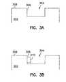
- FIGS. 3 A- 3 Billustrate an embodiment of a process of fabrication of conduction regions on a silicon wafer according to the teachings of the present invention.
- the sequencecan be followed as a method of forming an integrated circuit, as a method of forming a semiconductor device, as a method of forming an integrated circuit that includes a number of lateral transistors and as a method of forming a MOSFET device.
- FIG. 3Ashows the structure after the first sequence of processing.
- a trench 304is formed in a silicon wafer 302 using photolithography and etching techniques.
- the trench 304is specifically formed such that a trench wall 306 of the trench 304 has a ( 110 ) crystal plane orientation.
- the silicon wafer 302has a top surface 308 that has a ( 100 ) crystal plane.
- the top surface 308may have other specific crystal plane orientations (e.g., ( 111 ) crystal plane orientation).
- the silicon wafer 302includes a bulk silicon material.
- the silicon wafer 302includes a Silicon On Insulator (SOI) material.
- SOISilicon On Insulator
- FIG. 3Bshows the structure after the next sequence of processing.
- a semiconductor device 310is formed in the trench 304 using standard photolithography, etching, ion implantation and other processing techniques.
- the semiconductor device 310is formed lateral to the trench wall 306 .
- the semiconductor device 310is formed in the trench 304 such that it is capable of conducting an electrical current in a ⁇ 110 > direction.
- the electrical currentis capable of conducting an electrical current lateral to the trench wall 306 .
- the semiconductor device 310is a MOSFET device.
- the semiconductor device 310is a PMOS device.
- the semiconductor device 310is an NMOS device.
- FIG. 4illustrates one embodiment wherein an electrical current flow in a ⁇ 110 > direction.
- FIG. 4is a silicon structure having a top surface 402 .
- the top surface 402has a ( 100 ) crystal plane orientation.
- FIG. 4also illustrates a direction 404 coming from the top surface 402 , which is essentially perpendicular to such surface. Electrical current flow in direction 404 is in a ⁇ 100 > direction.
- the silicon structure of FIG. 4has a side surface 406 , which has a ( 110 ) crystal plane orientation.
- FIG. 4also illustrates a direction 408 , which runs essentially parallel to the side surface 406 and the top surface 402 . Electrical current flow in direction 408 is in a ⁇ 110 > direction.
- the room temperature hole mobility for a PMOS device and the resultant electrical current in the PMOS device formed according to the teachings of the present inventionis approximately two and a half times faster than a conventional planar device formed on a surface with a ( 100 ) crystal plane orientation. Because circuit performance is typically limited by the electrical current through PMOS devices, advantageously, a corresponding increase in performance for most logic applications generally occurs due to this increase in the speed of electrical current through PMOS devices.
- the graph of FIG. 5illustrates inversion layer hole mobility, expressed in velocity in centimeters per second divided by the field in V per centimeter, e.g. (cm 2 /Vsec), versus effective gate voltage, e.g. ⁇ (V G ⁇ V 96 ), expressed in volts (V), at a temperature of approximately 297° Kelvin (° K).
- FIG. 5includes a plot 502 and a plot 504 .
- the plot 502is the graphical plot of hole mobility versus a gate voltage for a MOSFET device on a silicon surface conducting in the ⁇ 100 > direction.
- the plot 504is the graphical plot of hole mobility versus a gate voltage for a MOSFET device on a silicon surface having a ( 110 ) crystalline plane orientation and conducting in the ⁇ 110 > direction. As illustrated in a region of normal operation 506 , the plot 504 has a hole mobility of approximately 250 cm 2 /V*sec. In contrast, as illustrated in the region of normal operation 506 , the plot 502 only has a hole mobility of approximately 100 cm 2 /V*sec.
- the formation and orientation of circuit devices lateral to surfaces having a ( 110 ) crystalline plane orientation in which the electrical current of such devices is flowing in the ⁇ 110 > directionallows for increases in the overall performance of such devices as well as of circuits which contain such devices.
- FIGS. 6 A- 6 Fillustrate a preferred embodiment of a process of fabrication of conduction regions on a silicon wafer according to the teachings of the present invention.
- the sequencecan be followed as a method of forming an integrated circuit, as a method of forming a semiconductor device, as a method of forming an integrated circuit that includes a number of lateral transistors and as a method of forming a MOSFET device.
- FIG. 6Ashows the structure after the first sequence of processing.
- a doped silicon layer 612is grown on silicon wafer 602 .
- the silicon wafer 602has a top surface 608 that has a ( 100 ) crystal plane orientation. However, it is important to appreciate that the top surface 608 may have other crystal plane orientations (e.g., ( 111 ) crystal plane orientation).
- the silicon wafer 602includes a bulk silicon material. In an alternative embodiment, the silicon wafer 602 includes a Silicon On Insulator (SOI) material.
- the doped silicon layer 612includes an n-type. In an alternative embodiment, the doped silicon layer 612 includes a p-type.
- FIG. 6Bshows the structure after the next sequence of processing.
- Trenches 604 a - bare formed in the doped silicon layer 612 , using conventional photolithography and etching techniques.
- the trenches 604 a - bare specifically formed such that a first and a second trench wall 606 and 610 of the trenches 604 a - b, respectively, have a ( 110 ) crystal plane orientation.
- FIG. 6Cshows the structure after the next sequence of processing.
- a thin silicon nitride (Si 3 Ni 4 ) layer 634is deposited by any suitable method, such as chemical vapor deposition (CVD), over the entire surface.
- the thin silicon nitride layer 634is selectively etched to leave a thin layer on the bottom of trenches 604 a - b.
- FIG. 6Dshows the structure after the next sequence of processing.
- a heavily doped glass layer 621which is of a different type than the type of the doped silicon layer 612 , is deposited across the entire surface.
- the doped silicon layer 612is an n-type semiconductor material, and the heavily doped glass layer 621 contains p-type dopant.
- the doped silicon layer 612is a p-type semiconductor material, and the heavily doped glass layer 621 contains n-type dopant.
- the heavily doped glass layer 621is deposited by any suitable means, such as by CVD.
- the heavily doped glass layer 621is then selectively etched to leave specific portions of the trenches 604 a - b, as shown in FIG. 6D.
- FIG. 6Eshows the structure after the next sequence of processing.
- the structureundergoes an anneal, such as a rapid thermal anneal (RTA), in order to drive the dopant species from the heavily doped glass layer 621 into the lateral walls of doped silicon layer 612 .
- RTArapid thermal anneal
- a first conductive region 614 or first conductive region of a first type 614is formed in the doped silicon layer 612 .
- a second conductive region 616 or second conductive region of a first type 616is also formed in the doped silicon layer 612 .
- the second conductive region 616is formed in reference to the first conductive region 614 to cause the formation of a third conductive region 618 or a conductive region of a second type 618 , in between the first conductive region 614 and the second conductive region 616 within the doped silicon layer 612 .
- a fourth conductive region 620 and a fifth conductive region 622are formed in the doped silicon layer 612 .
- the fifth conductive region 622is formed in reference to the fourth conductive region 620 to cause the formation of a sixth conductive region 624 in between the fourth conductive region 620 and the fifth conductive region 622 within the doped silicon layer 612 .
- the third and sixth conductive regions 618 and 624include an n-type semiconductor material. In another embodiment, the third and sixth conductive regions 616 and 624 include a p-type. In one embodiment, the third and sixth conductive regions 618 and 624 are of a different type conductive material in comparison with the first, second, fourth and fifth conductive regions 614 , 616 , 620 and 622 .
- an electrical currentis capable of flowing between the first conductive region 614 and the second conductive region 616 through the third conductive region 618 in a ⁇ 110 > direction, e.g. parallel to the top surface 608 of the silicon wafer 602 .
- the electrical currentis capable of flowing between the first conductive region 614 and the second conductive region 616 through the third conductive region 618 lateral to the first trench wall 606 .
- an electrical currentis capable of flowing between the fourth conductive region 620 and the fifth conductive region 622 through the sixth conductive region 624 in a ⁇ 110 > direction, e.g. parallel to the top surface 608 of the silicon wafer 602 .
- the electrical currentis capable of flowing between the fourth conductive region 620 and the fifth conductive region 622 through the sixth conductive region 624 lateral to the second trench wall 610 .
- FIG. 6Fshows the structure after the next sequence of processing.
- word lines 628 a and 628 b along with corresponding gate oxides 630 a and 630 bare formed lateral to the trench walls 606 and 610 of silicon wafer 602 , using standard photolithography and deposition techniques.
- word lines 628 a and 628 binclude gates formed lateral to the gate oxides, 630 a and 630 b respectively.
- word lines 628 a and 628 bare conductive lines constructed from a polysilicon.
- the configuration illustrated in FIG. 6Fincludes two access transistors used in conjunction with a DRAM.
- the third and sixth conductive regions 618 and 624are body regions of a transistor capable of forming a channel when a voltage potential is applied to the gates of such transistor. While only lateral transistors 640 and 650 are shown in FIG. 6F, one skilled in the art will recognize the repeatable structure shown and that any number of lateral transistors can be formed from the above described process and used in an array, hence, the details of a longer array are not disclosed in the present application.
- FIGS. 7 A- 7 Cillustrate another embodiment of a process of fabrication of conduction regions on a silicon wafer according to the teachings of the present invention.
- the sequencecan be followed as a method of forming an integrated circuit, as a method of forming a semiconductor device, as a method of forming an integrated circuit that includes a number of lateral transistors and as a method of forming a MOSFET device.
- FIG. 7Ashows the structure after the first sequence of processing.
- a doped silicon layer 712is grown on a silicon wafer 702 .
- the silicon wafer 702has a top surface 732 that has a ( 100 ) crystal plane orientation. However, it is important to appreciate that the top surface 732 may have other crystal plane orientations (e.g., ( 111 ) crystal plane orientation).
- the silicon wafer 702includes a bulk silicon material. In an alternative embodiment, the silicon wafer 702 includes a Silicon On Insulator (SOI) material.
- SOISilicon On Insulator
- the doped silicon layer 712includes an n-type. In an alternative embodiment, the doped silicon layer 712 includes a p-type. Additionally, a first conductive region 714 or first conductive region of a first type 714 is formed in the doped silicon layer 712 , using, for example, ion implantation techniques. A second conductive region 716 or second conductive region of a first type 716 is also formed in the doped silicon layer 712 . The second conductive region 716 can also be formed using, for example, ion implantation techniques.
- the second conductive region 716is formed in reference to the first conductive region 714 to cause the formation of a third conductive region 718 or a conductive region of a second type 718 , in between the first conductive region 714 and the second conductive region 716 within the doped silicon layer 712 .
- a fourth conductive region 720 and a fifth conductive region 722are formed in the doped silicon layer 712 , using, for example, ion implantation techniques.
- the fifth conductive region 722is formed in reference to the fourth conductive region 720 to cause the formation of a sixth conductive region 724 in between the fourth conductive region 720 and the fifth conductive region 722 within the doped silicon layer 712 .
- the first, second, fourth and fifth conductive regions 714 , 716 , 720 and 722include an n-type. In another embodiment, the first, second, fourth and fifth conductive regions 714 , 716 , 720 and 722 include a p-type. In one embodiment, the first and fourth conductive regions 714 and 720 are source regions and the second and fifth conductive regions 716 and 722 are drain regions of a transistor.
- FIG. 7Bshows the structure after the next sequence of processing.
- Trenches 704 a - bare etched in the silicon wafer 702 using conventional photolithography and etching techniques.
- the trenches 704 a - bare specifically etched such that a first and a second trench wall 708 and 710 of trenches 704 a - b, respectively, have a ( 110 ) crystal plane orientation.
- the first and the second trench walls 708 and 710are specifically etched in the first, second and third conductive regions and the fourth, fifth and sixth conductive regions, respectively, of the silicon wafer 102 .
- an electrical currentis capable of flowing between the first conductive region 714 and the second conductive region 716 through the third conductive region 718 in a ⁇ 110 > direction, e.g. parallel to the top surface 708 of the silicon wafer 702 .
- the electrical currentis capable of flowing between the first conductive region 714 and the second conductive region 716 through the third conductive region 718 lateral to the first trench wall 706 .
- an electrical currentis capable of flowing between the fourth conductive region 720 and the fifth conductive region 722 through the sixth conductive region 724 in a ⁇ 110 > direction, e.g. parallel to the top surface 708 of the silicon wafer 702 .
- the electrical currentis capable of flowing between the fourth conductive region 720 and the fifth conductive region 722 through the sixth conductive region 724 lateral to the second trench wall 710 .
- FIG. 7Cshows the structure after the next sequence of processing.
- word lines 728 a and 728 b along with corresponding gate oxides 730 a and 730 bare formed lateral to the trench walls 706 and 710 of silicon wafer 702 , using standard photolithography and deposition techniques.
- word lines 728 a and 728 binclude gates formed lateral to the gate oxides, 730 a and 730 b respectively.
- word lines 728 a and 728 bare conductive lines constructed from a polysilicon.
- the configuration illustrated in FIG. 7Cincludes two access transistors used in conjunction with a DRAM.
- the third and sixth conductive regions 718 and 724are body regions of a transistor capable of forming a channel when a voltage potential is applied to the gates of such transistor.
- the third and sixth conductive regions 718 and 724include an n-type semiconductor material.
- the third and sixth conductive regions 716 and 724include a p-type.
- the third and sixth conductive regions 718 and 724are of a different type conductive material in comparison with the first, second, fourth and fifth conductive regions 714 , 716 , 720 and 722 .
- lateral transistors 740 and 750are shown in FIG. 7C, one skilled in the art will recognize the repeatable structure shown and that any number of lateral transistors can be formed from the above described process and used in an array, hence, the details of a longer array are not disclosed in the present application.
- FIGS. 8 A- 8 Cillustrate another embodiment of a process of fabrication of conduction regions on a silicon wafer according to the teachings of the present invention.
- the sequencecan be followed as a method of forming an integrated circuit, as a method of forming a semiconductor device, as a method of forming an integrated circuit that includes a number of lateral transistors and as a method of forming a MOSFET device.
- FIG. 8Ashows the structure after the first sequence of processing.
- Trenches 804 a - bare formed in a silicon wafer 802 , using conventional photolithography and etching techniques.
- the trenches 804 a - bare specifically formed such that a first and a second trench wall 806 and 810 of the trenches 804 a - b, respectively, have a ( 110 ) crystal plane orientation.
- the silicon wafer 802has a top surface 808 that has a ( 100 ) crystal plane orientation.
- the top surface 808may have other crystal plane orientations (e.g., ( 111 ) crystal plane orientation).
- the silicon wafer 802includes a bulk silicon material.
- the silicon wafer 802includes a Silicon On Insulator (SOI) material.
- SOISilicon On Insulator
- FIG. 8Bshows the structure after the next sequence of processing.
- regions in the trench walls 806 and 810are doped using, for example, angled ion implantation, as shown.
- the doped regionsinclude (1) a first conductive region 814 or a first conductive region of a first type 814 , (2) a second conductive region 816 or a second conductive region of a first type 816 , (3) a fourth conductive region 820 , (4) a fifth conductive region 822 , and (5) a remaining region 826 of the top surface 808 .
- the remaining region 826includes a third conductive region 818 or a conductive region of a second type 818 and a sixth conductive region 824 .
- the doped regionsare formed such that the second conductive region 816 is formed in reference to the first conductive region 814 to cause the formation of the third conductive region 818 in between the first conductive region 814 and the second conductive region 816 . Additionally, the fifth conductive region 822 is formed in reference to the fourth conductive region 820 to cause the formation of the sixth conductive region 824 in between the fourth conductive region 820 and the fifth conductive region 822 .
- the remaining region 826which includes the third conductive region 818 and sixth conductive region 824 , is a different type conductive material in comparison with the first, second, fourth and fifth conductive regions 814 , 816 , 820 and 822 , respectively.
- the remaining region 826is an n-type, while the first, second, fourth and fifth conductive regions 814 , 816 , 820 and 822 , respectively, are a p-type.
- the remaining region 826is a p-type, and the first, second, fourth and fifth conductive regions 814 , 816 , 820 and 822 , respectively, are an n-type.
- the first and fourth conductive regions 814 and 820are source regions and the second and fifth conductive regions 816 and 822 are drain regions of a transistor.
- the third and sixth conductive regions 818 and 824are body regions of a transistor capable of forming a channel when a voltage potential is applied to the gates of such transistor.
- an electrical currentis capable of flowing between the first conductive region 814 and the second conductive region 816 through the third conductive region 818 in a ⁇ 110 > direction, e.g. parallel to the top surface 808 of the silicon wafer 802 .
- the electrical currentis capable of flowing between the first conductive region 814 and the second conductive region 816 through the third conductive region 818 lateral to the first trench wall 806 , which has a ( 110 ) crystal plane orientation.
- an electrical currentis capable of flowing between the fourth conductive region 820 and the fifth conductive region 822 through the sixth conductive region 824 in a ⁇ 110 > direction, e.g. parallel to the top surface 808 of the silicon wafer 802 .
- the electrical currentis capable of flowing between the fourth conductive region 820 and the fifth conductive region 822 through the sixth conductive region 824 lateral to the second trench wall 810 , which has a ( 110 ) crystal plane orientation.
- FIG. 8Cshows the structure after the next sequence of processing.
- word lines 828 a and 828 b along with corresponding gate oxides 830 a and 830 bare formed lateral to the trench walls 806 and 810 of silicon wafer 802 , using standard photolithography and deposition techniques.
- word lines 828 a and 828 binclude gates formed lateral to the gate oxides, 830 a and 830 b respectively.
- word lines 828 a and 828 bare conductive lines constructed from a polysilicon.
- the configuration illustrated in FIG. 8Cincludes two access transistors used in conjunction with a DRAM.
- lateral transistors 840 and 850are shown in FIG. 8C, one skilled in the art will recognize the repeatable structure shown and that any number of lateral transistors can be formed from the above described process and used in an array, hence, the details of a longer array are not disclosed in the present application.
- FIG. 9is a cross-sectional view of an embodiment of an integrated circuit according to the teachings of the present invention.
- the integrated circuit of FIG. 9is constructed in a similar manner according to any one of the methods presented in this application.
- the integrated circuitincludes a trench wall 906 of a trench 904 in a silicon wafer 902 .
- the trench wall 906has a ( 110 ) crystal plane orientation.
- the silicon wafer 902has a top surface 908 that has a ( 100 ) crystal plane orientation. However, it is important to appreciate that the top surface 908 may have other crystal plane orientations (e.g., ( 111 ) crystal plane orientation).
- the silicon wafer 902includes a bulk silicon material.
- the silicon wafer 902includes a Silicon On Insulator (SOI) material.
- SOISilicon On Insulator
- the integrated circuit of FIG. 9also includes a semiconductor device 910 which is lateral to the trench wall 906 .
- the semiconductor device 910is designed for or configured for conducting an electrical current in the ⁇ 110 > direction.
- the semiconductor device 910is a MOSFET device.
- the semiconductor device 910is a p-MOSFET device.
- the semiconductor device 910is a n-MOSFET device.
- FIG. 10is a cross-sectional view of an embodiment of a device according to the teachings of the present invention.
- the device of FIG. 10is constructed in a similar manner according to any one of the methods presented in this application.
- the device of FIG. 10is a semiconductor device.
- the device of FIG. 10is a MOSFET device.
- the deviceis an n-MOSFET device.
- the deviceis a p-MOSFET device.
- the deviceis a portion of a dynamic random access memory (DRAM) having an array of transistors.
- the deviceis a portion of an array of MOSFETs.
- the device of FIG. 10is a portion of an integrated circuit.
- DRAMdynamic random access memory
- the deviceincludes a first conductive region 1010 in a trench 1004 of a silicon wafer 1002 .
- the first conductive region 1010is of a first type and is lateral to a trench wall 1006 of the trench 1004 . Additionally, the trench wall 1006 has a ( 110 ) crystal plane orientation.
- the first typeis an n-type. In another embodiment, the first type is a p-type.
- the silicon wafer 1002has a top surface 1008 , which has a ( 100 ) crystal plane orientation.
- the device of FIG. 10also includes a second conductive region 1012 in the trench 1004 .
- the second conductive region 1012is of the first type and is lateral to the trench wall 1006 .
- the device of FIG. 10includes a third conductive region 1014 in the trench 1004 .
- the third conductive region 1014is of a second type and is lateral to the trench wall 1006 .
- An electrical currentis also capable of flowing between the first conductive region 1010 and the second conductive region 1012 in a ⁇ 110 > direction.
- the third conductive region 1014is a body region of a MOSFET device.
- FIG. 11is a block diagram which illustrates an embodiment of a system 1100 according to teachings of the present invention.
- the system 1100includes an integrated circuit 1110 which can include a memory, e.g. a DRAM.
- the integrated circuit 1110includes the embodiments of a device in a trench of a semiconductor wafer according to the structures and methods described above in this application.
- the deviceis lateral to a trench wall of the trench such that the trench wall has a ( 110 ) crystal plane orientation and an electrical current is capable of flowing in the device in a ⁇ 110 > direction, all according to the teachings of the present invention.
- the system 1100includes a processor 1120 that is operatively coupled to the integrated circuit 1110 .
- the processor 1120is coupled to the integrated circuit 1110 through a bus 1130 .
- the processor 1120 and the integrated circuit 1110are on the same semiconductor chip.
- improved methods and structuresare provided that are lateral to surfaces with a ( 110 ) crystal plane orientation such that an electrical current of such structures is in a ⁇ 110 > direction.
- improvements in hole carrier mobility of approximately 50%can be obtained by orienting the structure's channel in a ( 110 ) plane such that the electrical current flow is in the ⁇ 110 > direction.
- these improved methods and structurescan be used in conjunction with existing fabrication and processing techniques with minimal or no added complexity.
Landscapes
- Engineering & Computer Science (AREA)
- Manufacturing & Machinery (AREA)
- Metal-Oxide And Bipolar Metal-Oxide Semiconductor Integrated Circuits (AREA)
- Insulated Gate Type Field-Effect Transistor (AREA)
- Thin Film Transistor (AREA)
Abstract
Description
- This application is related to co-pending and co-filed application Ser. No. xx/xxx,xxx, attorney docket number 303.604US1, filed on even date herewith, entitled “Multiple Oxide Thicknesses for Merged Memory and Logic Applications” by inventors Leonard Forbes and William P. Noble, which is hereby incorporated by reference. This application is further related to co-pending and co-filed application Ser. No. xx/xxx,xxx, attorney docket number M4065.180/P180, filed on even date herewith, entitled “Vertical Sub-Micron CMOS Transistors on ([0001]110), (111), (311), (511), and Higher Order Surfaces of Bulk, SOI and Thin Film Structures and Method of Forming Same,” by inventors Leonard Forbes, William P. Noble and Alan R. Reinberg, which is hereby incorporated by reference. This application is also related to co-pending and co-filed application Ser. No. xx/xxx,xxx, attorney docket number M4065.0204/P204, filed on even date herewith, entitled “Method for Fabricating CMOS Transistors Having Matching Characteristics and Apparatus Formed Thereby,” by inventors Leonard Forbes and William P. Noble, which is hereby incorporated by reference.
- The present invention relates to integrated circuits, and more particularly, to a method, a structure and a system for providing semiconductor devices on ([0002]110) surfaces with conduction in the <110> direction.
- In general, the standard silicon wafer crystal orientation for VLSI (Very Large Scale Integration) is the ([0003]100) orientation. This surface orientation was chosen over the previously used (111) crystal orientation because of its comparatively low surface state density on thermally oxidized surfaces. In particular, a (111) crystal orientation has a surface state charge density of approximately 5×10¹¹e/centimeters2(cm2) in comparison with a (100) crystal orientation which has a surface state charge density of approximately 9×10¹⁰e/cm2.
- Surface state density was a particularly important consideration for n-channel Metal Oxide Semiconductor (NMOS) technologies because the higher this surface state density level the more difficult the controlling of active and parasitic device threshold voltages for devices using such technologies. For ([0004]110) surfaces, the surface state charge density is approximately 2×10¹¹e/cm2which is approximately twice the density level for (100) surfaces. In present day technology, this difference in density levels translates into less than 0.09 volts offset in active device threshold voltage and is readily compensated by a surface threshold voltage ion implant. A further benefit to a lower surface state charge density for NMOS devices is that the electron mobility in inversion layers is greater on the (100) surface than on other lower order planes.
- However, for modem day complimentary metal oxide semiconductor (CMOS) technology involving sub-micron devices, a different set of trade-offs are involved. For such short channel devices, the NMOS devices operate largely in velocity saturation resulting in a source to drain current which is independent of crystal orientation.[0005]
- In contrast as illustrated in FIGS. 1 and 2, p-channel Metal Oxide Semiconductor (PMOS) devices are less likely to operate in velocity saturation, and therefore are more dependent on the choice of crystal orientation around inversion layer hole mobility. In particular, FIG. 1 includes a[0006]
transistor 100, which can be either an NMOS or PMOS transistor.Transistor 100 is comprised of asilicon wafer 102, asource region 104, adrain region 106, agate 108, anoxide layer 110, abody region 111 and achannel region 112 between thesource region 104 and thedrain region 106. As is well-known in the art, a voltage differential between thesource region 104 and thedrain region 106 induces an electric field across thechannel region 112. A gate potential applied to thegate 108 can create an inversion layer in thebody region 111 allowing thechannel region 112 to form between thesource region 104 and thedrain region 106. This electric field is expressed in terms of the voltage differential between thesource region 104 and thedrain region 106 per the length of thechannel region 112. - FIG. 2 illustrates a graph of the drift velocity for carriers (i.e., either holes or electrons) across the[0007]
channel region 112, expressed in cm/second (sec), versus an average source-to-drain electric field, expressed in volts/cm. In particular, aplot 202 is the graphical plot of the drift velocity of electrons in the channel of an NMOS versus the electric field generated by the voltage differential between thesource region 104 and thedrain region 106. Additionally, aplot 204 is the graphical plot of the drift velocity of holes in the channel of a PMOS versus the electric field generated by the voltage differential between thesource region 104 and thedrain region 106. As illustrated, theplot 202 reaches velocity saturation at approximately 104V/cm (i.e., the point in which the graphical plot flattens). In contrast in the graph of FIG. 2, theplot 204 has not reached the point of velocity saturation, even at 105V/cm. Thus, a PMOS device that uses holes as carriers is more dependent on the choice of crystal orientation for inversion hole mobility. - Currently, surfaces with a ([0008]110) crystal plane orientation have been explored in the planar bulk and Silicon On Insulator (SOI) technologies by using (110) substrate wafers or causing the recrystallization of the surface of a substrate wafer to have a (110) crystal orientation. However, these structures and methods require re-tooling of crystal growth mechanisms used in conjunction with the standard (100) crystalline plane orientation and/or otherwise introduce costly, additional processing steps and procedures.
- Thus, there is a need for structures and methods which improve carrier mobility in semiconductor devices and which do so without the introduction of costly additional processing steps or which require any re-tooling of standard crystal growth mechanisms. For these and other reasons there is a need for the present invention.[0009]
- The above-mentioned problems and limitations associated with carrier mobility in semiconductor devices and other problems are addressed by the present invention and will be understood by reading and studying the following specification. Structures and methods are described which accord improved benefits.[0010]
- Improved methods and structures are provided that are lateral to surfaces with a ([0011]110) crystal plane orientation in which an electrical current of such structures is in a <110> direction. Advantageously, improvements in carrier mobility of approximately 50% can be obtained by orienting the structure's channel in a (110) plane such that the electrical current flow is in the <110> direction. Moreover, these improved methods and structures can be used in conjunction with existing fabrication and processing techniques with minimal or no added complexity.
- Embodiments of a method of forming an integrated circuit include forming a trench in a silicon wafer. A trench wall of the trench has a ([0012]110) crystal plane orientation. A semiconductor device is also formed lateral to the trench wall such that the semiconductor device is capable of conducting an electrical current in a <110> direction.
- One method of the present invention provides for forming an integrated circuit. Another method includes forming an integrated circuit including an array of MOSFETs while another method includes forming an integrated circuit including a number of lateral transistors. Another method includes forming a semiconductor device. Moreover, other embodiments provide for forming MOSFET devices (e.g., PMOS and NMOS devices). The present invention also includes structures as well as systems incorporating such structures all formed according to the methods provided in this application.[0013]
- These and other embodiments, aspects, advantages, and features of the present invention will be set forth in part in the description which follows, and in part will become apparent to those skilled in the art by reference to the following description of the invention and referenced drawings or by practice of the invention. The aspects, advantages, and features of the invention are realized and attained by means of the instrumentalities, procedures, and combinations particularly pointed out in the appended claims.[0014]
- FIG. 1 is a cross-sectional view of a MOSFET device.[0015]
- FIG. 2 is a graph that illustrates a drift velocity of carriers of a MOSFET device vs. average source-to-drain electric field for the MOSFET device.[0016]
- FIGS.[0017]3A-3B illustrate an embodiment of a process of fabrication of conduction regions on a silicon wafer according to the teachings of the present invention.
- FIG. 4 is a silicon structure illustrating embodiments of crystal plane orientations of surfaces and electrical current flow directions.[0018]
- FIG. 5 is a graph that illustrates inversion layer hole mobility vs. effective gate voltage.[0019]
- FIGS.[0020]6A-6F illustrate an embodiment of a process of fabrication of conduction regions on a silicon wafer according to the teachings of the present invention.
- FIGS.[0021]7A-7C illustrate another embodiment of a process of fabrication of conduction regions on a silicon wafer according to the teachings of the present invention.
- FIGS.[0022]8A-8C illustrate another embodiment of a process of fabrication of conduction regions on a silicon wafer according to the teachings of the present invention.
- FIG. 9 is a cross-sectional view of an embodiment of an integrated circuit according to the teachings of the present invention.[0023]
- FIG. 10 is a cross-sectional view of an embodiment of a semiconductor device according to the teachings of the present invention.[0024]
- FIG. 11 is a block diagram which illustrates an embodiment of a system according to teachings of the present invention.[0025]
- In the following detailed description of the invention, reference is made to the accompanying drawings which form a part hereof, and in which is shown, by way of illustration, specific embodiments in which the invention may be practiced. In the drawings, like numerals describe substantially similar components throughout the several views. These embodiments are described in sufficient detail to enable those skilled in the art to practice the invention. Other embodiments may be utilized and structural, logical, and electrical changes may be made without departing from the scope of the present invention.[0026]
- The terms wafer and substrate used in the following description include any structure having an exposed surface with which to form the integrated circuit (IC) structure of the invention. The term substrate is understood to include semiconductor wafers. The term substrate is also used to refer to semiconductor structures during processing, and may include other layers that have been fabricated thereupon. Both wafer and substrate include doped and undoped semiconductors, epitaxial semiconductor layers supported by a base semiconductor or insulator, as well as other semiconductor structures well known to one skilled in the art. The term conductor is understood to include semiconductors, and the term insulator is defined to include any material that is less electrically conductive than the materials referred to as conductors. The following detailed description is, therefore, not to be taken in a limiting sense, and the scope of the present invention is defined only by the appended claims, along with the full scope of equivalents to which such claims are entitled.[0027]
- In particular, an illustrative embodiment of the present invention includes a method of forming an integrated circuit. The method includes forming a trench in a silicon wafer. A trench wall of the trench has a ([0028]110) crystal plane orientation. Additionally, a semiconductor device is formed lateral to the trench wall. Moreover, the semiconductor device is capable of conducting an electrical current in a <110> direction.
- Another embodiment of the present invention includes a method of forming a semiconductor device. This method includes forming a first conductive region of a first type in a trench of a silicon wafer. In particular, the first conductive region of the first type is lateral to a trench wall of the trench with the trench wall having a ([0029]110) crystal plane orientation. Moreover, a second conductive region of the first type is formed in the trench. The second conductive region of the first type is formed lateral to the trench wall. The method also includes forming a conductive region of a second type in the trench. In particular, this conductive region of the second type is lateral to the trench wall and between the first and second conductive regions of the first type. Additionally, an electrical current is capable of flowing between the first and the second conductive regions of the first type in a <110> direction.
- An alternative method embodiment of the present invention includes forming an integrated circuit which includes a number of lateral transistors. The method includes forming a trench in a silicon wafer, which has a top surface having a ([0030]100) crystal plane orientation. Additionally, the trench has a trench wall with a (110) crystal plane orientation. The method also includes forming a first conductive region in a first portion of the trench. In particular, this first conductive region is lateral to the trench wall. Moreover, a second conductive region is formed in a second portion of the trench such that this second conductive region is lateral to the trench wall. The method also includes forming a third conductive region in a third portion of the trench. This third conductive region is lateral to the trench wall and between the first and second conductive regions. Moreover, an electrical current is capable of flowing between the first conductive region and the second conductive region in a <110> direction.
- Another method embodiment of the present invention includes forming a p-channel Metal Oxide Semiconductor Field Effect Transistor (p-MOSFET) device. This method includes forming a trench in a silicon wafer such that the trench includes a trench wall having a ([0031]110) crystal plane orientation. Additionally, a first conductive p-type region is formed in the trench of the silicon wafer. In particular, this first conductive p-type region is lateral to the trench wall of the trench. The method also includes forming a second conductive p-type region in the trench such that the second conductive p-type region is lateral to the trench wall. Further a conductive n-type region is formed in the trench. This conductive n-type region is formed lateral to the trench wall and between the first and second conductive p-type regions. Additionally, the p-MOSFET device is configured for conducting an electrical current between the first and the second conductive p-type regions in a direction lateral to the trench wall.
- An additional method embodiment of the present invention includes forming an integrated circuit including an array of Metal Oxide Semiconductor Field Effect Transistors (MOSFETs). The method includes forming a number of trenches in a silicon wafer such that the number of trenches have a trench wall in a ([0032]110) crystalline plane orientation. The method also includes forming a number of spaced MOSFETs in each trench. The formation of the number of spaced MOSFETs includes forming a first conductive p-type region in the trench of the silicon wafer such that the first conductive p-type region is lateral to the trench wall of the trench. Further, a second conductive p-type region is formed in the trench such that the second conductive p-type region is lateral to the trench wall. The formation of the number of spaced MOSFETs also includes forming a conductive n-type region in the trench such that the conductive n-type region is lateral to the trench wall and between the first and the second conductive p-type regions. Additionally, an electrical current is capable of flowing between the first and the second p-type regions in a <110> direction.
- An apparatus embodiment of the present invention includes an integrated circuit. The integrated circuit includes a trench wall in a silicon wafer in which the trench wall has a ([0033]110) crystal plane orientation. The integrated circuit also includes a semiconductor device lateral to the trench wall. Moreover, the semiconductor device is configured to conduct an electrical current in the <110> direction.
- Another apparatus embodiment of the present invention includes a semiconductor device. The semiconductor device includes a first conductive region of a first type in a trench of a silicon wafer. This first conductive region of the first type is lateral to a trench wall of the trench, and the trench wall has a ([0034]110) crystal plane orientation. The semiconductor device also includes a second conductive region of the first type in the trench. This second conductive region of the first type is lateral to the trench wall. Additionally, the semiconductor device includes a conductive region of a second type in the trench. This conductive region of the second type is lateral to the trench wall and between the first and second conductive regions of the first type. Moreover, the semiconductor device is designed to conduct an electrical current between the first and second conductive regions of the first type in a <110> direction.
- An alternative apparatus embodiment of the present invention includes a dynamic random access memory (DRAM). The DRAM includes an array of lateral transistors formed on a trench wall of a trench in a silicon wafer such that the silicon wafer has a top surface in a ([0035]100) crystal plane orientation and the trench wall has a (110) crystal plane orientation. Additionally, each lateral transistor includes a first conductive region in a first portion of the trench wall. Each lateral transistor also includes a second conductive region in a second portion of the trench wall. Further, each lateral transistor includes a third conductive region in a third portion of the trench wall, such that the third conductive region is between the first and second conductive regions. Additionally, each lateral transistor is configured to conduct an electrical current between the first conductive regions and the second conductive region in a <110> direction. The DRAM also includes a wordline coupled to a gate of each lateral transistor formed on the trench wall of the trench of the silicon wafer.
- Another apparatus embodiment of the present invention includes a p-channel Metal Oxide Semiconductor Field Effect Transistor (p-MOSFET) device. The p-MOSFET device includes a first conductive p-type region in a trench of a silicon wafer. This first conductive p-type region is lateral to a trench wall of the trench with the trench wall having a ([0036]110) crystal plane orientation. The p-MOSFET device also includes a second conductive p-type region in the trench in which the second conductive p-type region is lateral to the trench wall. Additionally, the p-MOSFET device includes a conductive n-type region in the trench. This conductive n-type region is lateral to the trench wall and between the first and second conductive p-type regions. Moreover, an electrical current is capable of flowing between the first and second conductive p-type regions in a direction lateral to the trench wall.
- Another apparatus embodiment of the present invention includes an array of Metal Oxide Semiconductor Field Effect Transistors (MOSFETs). The array of MOSFETs includes a number of trenches formed in a silicon wafer. The array of MOSFETs also includes a number of spaced MOSFETs in each trench. Each MOSFET includes a first conductive p-type region in a trench of the silicon wafer such that the first conductive p-type region is lateral to a trench wall of the trench. The trench wall has a ([0037]110) crystal plane orientation. Each MOSFET also includes a second conductive p-type region in the trench such that the second conductive p-type region is lateral to the trench wall. Further, each MOSFET includes a conductive n-type region in the trench such that the conductive n-type region is lateral to the trench wall and between the first and second conductive p-type regions. Additionally, an electrical current is capable of flowing between the first and second conductive p-type regions in a <110> direction.
- An alternative apparatus embodiment of the present invention includes an electronic system. This electronic system includes a processor. This electronic system also includes an integrated circuit coupled to the processor. In particular, the integrated circuit is formed on a silicon wafer. The silicon wafer includes a trench wall that has a ([0038]110) crystal plane orientation. The silicon wafer also includes a semiconductor device lateral to the trench wall. The semiconductor device is capable of conducting an electrical current in a <110> direction.
- Another apparatus embodiment of the present invention includes an electronic system. The electronic system includes a processor as well as a semiconductor device coupled to the processor. The semiconductor device includes a first conductive region of a first type in a trench of a silicon wafer. In particular, the first conductive region of the first type is lateral to a trench wall of the trench, and the trench wall has a ([0039]110) crystal plane orientation. The semiconductor device also includes a second conductive region of the first type in the trench. This second conductive region of the first type is lateral to the trench wall. Additionally, the semiconductor device includes a conductive region of a second type in the trench. In particular, the conductive region of the second type is lateral to the trench wall and between the first and second conductive regions of the first type. Moreover, an electrical current is capable of flowing between the first and second conductive regions of the first type in a <110> direction.
- An alternative apparatus embodiment of the present invention includes an electronic system. The electronic system includes a processor as well as a memory coupled to the processor. The memory includes an array of lateral transistors formed on a trench wall of a trench in a silicon wafer. The silicon wafer has a top surface with a ([0040]100) crystal plane orientation, and the trench wall has a (110) crystal plane orientation. Additionally, each lateral transistor in the array of lateral transistors includes a first conductive region in a first portion of the trench in which the first conductive region is lateral to the trench wall. Moreover, each lateral transistor includes a second conductive region in a second portion of the trench. In particular, this second conductive region is lateral to the trench wall. Each lateral transistor also includes a third conductive region in a third portion of the trench. This third conductive region is lateral to the trench wall and between the first and second conductive regions. Moreover, an electrical current is capable of flowing between the first conductive region and the second conductive region in a <110> direction.
- FIGS.[0041]3A-3B illustrate an embodiment of a process of fabrication of conduction regions on a silicon wafer according to the teachings of the present invention. The sequence can be followed as a method of forming an integrated circuit, as a method of forming a semiconductor device, as a method of forming an integrated circuit that includes a number of lateral transistors and as a method of forming a MOSFET device.
- FIG. 3A shows the structure after the first sequence of processing. A[0042]
trench 304 is formed in asilicon wafer 302 using photolithography and etching techniques. One of ordinary skill in the art will understand the manner in which photolithography and etching techniques can be used to form a trench in a silicon wafer. According to the teachings of the present invention, thetrench 304 is specifically formed such that atrench wall 306 of thetrench 304 has a (110) crystal plane orientation. In one embodiment, thesilicon wafer 302 has atop surface 308 that has a (100) crystal plane. However, it is important to appreciate that thetop surface 308 may have other specific crystal plane orientations (e.g., (111) crystal plane orientation). In one embodiment, thesilicon wafer 302 includes a bulk silicon material. In an alternative embodiment, thesilicon wafer 302 includes a Silicon On Insulator (SOI) material. - FIG. 3B shows the structure after the next sequence of processing. A semiconductor device[0043]310 is formed in the
trench 304 using standard photolithography, etching, ion implantation and other processing techniques. In particular, the semiconductor device310 is formed lateral to thetrench wall 306. Moreover, in one embodiment, the semiconductor device310 is formed in thetrench 304 such that it is capable of conducting an electrical current in a <110> direction. In one embodiment, the electrical current is capable of conducting an electrical current lateral to thetrench wall 306. In one embodiment, the semiconductor device310 is a MOSFET device. In one such embodiment, the semiconductor device310 is a PMOS device. In another such embodiment, the semiconductor device310 is an NMOS device. - FIG. 4 illustrates one embodiment wherein an electrical current flow in a <[0044]110> direction. In particular, FIG. 4 is a silicon structure having a
top surface 402. According to the teachings of the present invention, thetop surface 402 has a (100) crystal plane orientation. FIG. 4 also illustrates adirection 404 coming from thetop surface 402, which is essentially perpendicular to such surface. Electrical current flow indirection 404 is in a <100> direction. Additionally, the silicon structure of FIG. 4 has aside surface 406, which has a (110) crystal plane orientation. FIG. 4 also illustrates adirection 408, which runs essentially parallel to theside surface 406 and thetop surface 402. Electrical current flow indirection 408 is in a <110> direction. - As illustrated in FIG. 5, the room temperature hole mobility for a PMOS device and the resultant electrical current in the PMOS device formed according to the teachings of the present invention is approximately two and a half times faster than a conventional planar device formed on a surface with a ([0045]100) crystal plane orientation. Because circuit performance is typically limited by the electrical current through PMOS devices, advantageously, a corresponding increase in performance for most logic applications generally occurs due to this increase in the speed of electrical current through PMOS devices.
- In particular, the graph of FIG. 5 illustrates inversion layer hole mobility, expressed in velocity in centimeters per second divided by the field in V per centimeter, e.g. (cm[0046]2/Vsec), versus effective gate voltage, e.g. −(VG−V96), expressed in volts (V), at a temperature of approximately 297° Kelvin (° K). FIG. 5 includes a
plot 502 and aplot 504. Theplot 502 is the graphical plot of hole mobility versus a gate voltage for a MOSFET device on a silicon surface conducting in the <100> direction. Theplot 504 is the graphical plot of hole mobility versus a gate voltage for a MOSFET device on a silicon surface having a (110) crystalline plane orientation and conducting in the <110> direction. As illustrated in a region ofnormal operation 506, theplot 504 has a hole mobility of approximately 250 cm2/V*sec. In contrast, as illustrated in the region ofnormal operation 506, theplot 502 only has a hole mobility of approximately 100 cm2/V*sec. Thus, according to the teachings of the present invention, the formation and orientation of circuit devices lateral to surfaces having a (110) crystalline plane orientation in which the electrical current of such devices is flowing in the <110> direction allows for increases in the overall performance of such devices as well as of circuits which contain such devices. - FIGS.[0047]6A-6F illustrate a preferred embodiment of a process of fabrication of conduction regions on a silicon wafer according to the teachings of the present invention. The sequence can be followed as a method of forming an integrated circuit, as a method of forming a semiconductor device, as a method of forming an integrated circuit that includes a number of lateral transistors and as a method of forming a MOSFET device.
- FIG. 6A shows the structure after the first sequence of processing. A doped[0048]
silicon layer 612 is grown onsilicon wafer 602. In one embodiment, thesilicon wafer 602 has atop surface 608 that has a (100) crystal plane orientation. However, it is important to appreciate that thetop surface 608 may have other crystal plane orientations (e.g., (111) crystal plane orientation). In one embodiment, thesilicon wafer 602 includes a bulk silicon material. In an alternative embodiment, thesilicon wafer 602 includes a Silicon On Insulator (SOI) material. In one embodiment, the dopedsilicon layer 612 includes an n-type. In an alternative embodiment, the dopedsilicon layer 612 includes a p-type. - FIG. 6B shows the structure after the next sequence of processing. Trenches[0049]604a-bare formed in the doped
silicon layer 612, using conventional photolithography and etching techniques. In particular, the trenches604a-bare specifically formed such that a first and asecond trench wall - FIG. 6C shows the structure after the next sequence of processing. A thin silicon nitride (Si[0050]3Ni4)
layer 634 is deposited by any suitable method, such as chemical vapor deposition (CVD), over the entire surface. The thinsilicon nitride layer 634 is selectively etched to leave a thin layer on the bottom of trenches604a-b. - FIG. 6D shows the structure after the next sequence of processing. A heavily doped[0051]
glass layer 621, which is of a different type than the type of the dopedsilicon layer 612, is deposited across the entire surface. In one such embodiment, the dopedsilicon layer 612 is an n-type semiconductor material, and the heavily dopedglass layer 621 contains p-type dopant. In another such embodiment, the dopedsilicon layer 612 is a p-type semiconductor material, and the heavily dopedglass layer 621 contains n-type dopant. The heavily dopedglass layer 621 is deposited by any suitable means, such as by CVD. The heavily dopedglass layer 621 is then selectively etched to leave specific portions of the trenches604a-b,as shown in FIG. 6D. - FIG. 6E shows the structure after the next sequence of processing. The structure undergoes an anneal, such as a rapid thermal anneal (RTA), in order to drive the dopant species from the heavily doped[0052]
glass layer 621 into the lateral walls of dopedsilicon layer 612. Accordingly, a firstconductive region 614 or first conductive region of afirst type 614 is formed in the dopedsilicon layer 612. A secondconductive region 616 or second conductive region of afirst type 616 is also formed in the dopedsilicon layer 612. In particular, the secondconductive region 616 is formed in reference to the firstconductive region 614 to cause the formation of a thirdconductive region 618 or a conductive region of asecond type 618, in between the firstconductive region 614 and the secondconductive region 616 within the dopedsilicon layer 612. - Further, a fourth[0053]
conductive region 620 and a fifthconductive region 622 are formed in the dopedsilicon layer 612. In particular, the fifthconductive region 622 is formed in reference to the fourthconductive region 620 to cause the formation of a sixthconductive region 624 in between the fourthconductive region 620 and the fifthconductive region 622 within the dopedsilicon layer 612. - In one embodiment, the third and sixth[0054]
conductive regions conductive regions conductive regions conductive regions - Additionally, an electrical current is capable of flowing between the first[0055]
conductive region 614 and the secondconductive region 616 through the thirdconductive region 618 in a <110> direction, e.g. parallel to thetop surface 608 of thesilicon wafer 602. In one embodiment, the electrical current is capable of flowing between the firstconductive region 614 and the secondconductive region 616 through the thirdconductive region 618 lateral to thefirst trench wall 606. - Further, an electrical current is capable of flowing between the fourth[0056]
conductive region 620 and the fifthconductive region 622 through the sixthconductive region 624 in a <110> direction, e.g. parallel to thetop surface 608 of thesilicon wafer 602. In one embodiment, the electrical current is capable of flowing between the fourthconductive region 620 and the fifthconductive region 622 through the sixthconductive region 624 lateral to thesecond trench wall 610. - FIG. 6F shows the structure after the next sequence of processing. In particular, word lines[0057]628aand628balong with corresponding
gate oxides trench walls silicon wafer 602, using standard photolithography and deposition techniques. In one embodiment, word lines628aand628binclude gates formed lateral to the gate oxides,630aand630brespectively. In one embodiment, word lines628aand628bare conductive lines constructed from a polysilicon. In one embodiment, the configuration illustrated in FIG. 6F includes two access transistors used in conjunction with a DRAM. - In one embodiment, the third and sixth[0058]
conductive regions lateral transistors 640 and650 are shown in FIG. 6F, one skilled in the art will recognize the repeatable structure shown and that any number of lateral transistors can be formed from the above described process and used in an array, hence, the details of a longer array are not disclosed in the present application. - FIGS.[0059]7A-7C illustrate another embodiment of a process of fabrication of conduction regions on a silicon wafer according to the teachings of the present invention. The sequence can be followed as a method of forming an integrated circuit, as a method of forming a semiconductor device, as a method of forming an integrated circuit that includes a number of lateral transistors and as a method of forming a MOSFET device.
- FIG. 7A shows the structure after the first sequence of processing. A doped[0060]
silicon layer 712 is grown on asilicon wafer 702. In one embodiment, thesilicon wafer 702 has atop surface 732 that has a (100) crystal plane orientation. However, it is important to appreciate that thetop surface 732 may have other crystal plane orientations (e.g., (111) crystal plane orientation). In one embodiment, thesilicon wafer 702 includes a bulk silicon material. In an alternative embodiment, thesilicon wafer 702 includes a Silicon On Insulator (SOI) material. - In one embodiment, the doped[0061]
silicon layer 712 includes an n-type. In an alternative embodiment, the dopedsilicon layer 712 includes a p-type. Additionally, a firstconductive region 714 or first conductive region of afirst type 714 is formed in the dopedsilicon layer 712, using, for example, ion implantation techniques. A secondconductive region 716 or second conductive region of afirst type 716 is also formed in the dopedsilicon layer 712. The secondconductive region 716 can also be formed using, for example, ion implantation techniques. In particular, the secondconductive region 716 is formed in reference to the firstconductive region 714 to cause the formation of a thirdconductive region 718 or a conductive region of asecond type 718, in between the firstconductive region 714 and the secondconductive region 716 within the dopedsilicon layer 712. - Further, a fourth[0062]
conductive region 720 and a fifthconductive region 722 are formed in the dopedsilicon layer 712, using, for example, ion implantation techniques. In particular, the fifthconductive region 722 is formed in reference to the fourthconductive region 720 to cause the formation of a sixthconductive region 724 in between the fourthconductive region 720 and the fifthconductive region 722 within the dopedsilicon layer 712. - In one embodiment, the first, second, fourth and fifth[0063]
conductive regions conductive regions conductive regions conductive regions - FIG. 7B shows the structure after the next sequence of processing. Trenches[0064]704a-bare etched in the
silicon wafer 702 using conventional photolithography and etching techniques. In particular, the trenches704a-bare specifically etched such that a first and asecond trench wall second trench walls silicon wafer 102. - Additionally, an electrical current is capable of flowing between the first[0065]
conductive region 714 and the secondconductive region 716 through the thirdconductive region 718 in a <110> direction, e.g. parallel to thetop surface 708 of thesilicon wafer 702. In one embodiment, the electrical current is capable of flowing between the firstconductive region 714 and the secondconductive region 716 through the thirdconductive region 718 lateral to the first trench wall706. - Further, an electrical current is capable of flowing between the fourth[0066]
conductive region 720 and the fifthconductive region 722 through the sixthconductive region 724 in a <110> direction, e.g. parallel to thetop surface 708 of thesilicon wafer 702. In one embodiment, the electrical current is capable of flowing between the fourthconductive region 720 and the fifthconductive region 722 through the sixthconductive region 724 lateral to thesecond trench wall 710. - FIG. 7C shows the structure after the next sequence of processing. In particular, word lines[0067]728aand728balong with corresponding
gate oxides 730aand730bare formed lateral to thetrench walls 706 and710 ofsilicon wafer 702, using standard photolithography and deposition techniques. In one embodiment, word lines728aand728binclude gates formed lateral to the gate oxides,730aand730brespectively. In one embodiment, word lines728aand728bare conductive lines constructed from a polysilicon. In one embodiment, the configuration illustrated in FIG. 7C includes two access transistors used in conjunction with a DRAM. - In one embodiment, the third and sixth[0068]
conductive regions conductive regions conductive regions conductive regions conductive regions - While only[0069]
lateral transistors 740 and750 are shown in FIG. 7C, one skilled in the art will recognize the repeatable structure shown and that any number of lateral transistors can be formed from the above described process and used in an array, hence, the details of a longer array are not disclosed in the present application. - FIGS.[0070]8A-8C illustrate another embodiment of a process of fabrication of conduction regions on a silicon wafer according to the teachings of the present invention. The sequence can be followed as a method of forming an integrated circuit, as a method of forming a semiconductor device, as a method of forming an integrated circuit that includes a number of lateral transistors and as a method of forming a MOSFET device.
- FIG. 8A shows the structure after the first sequence of processing. Trenches[0071]804a-bare formed in a
silicon wafer 802, using conventional photolithography and etching techniques. In particular, the trenches804a-bare specifically formed such that a first and asecond trench wall silicon wafer 802 has atop surface 808 that has a (100) crystal plane orientation. However, it is important to appreciate that thetop surface 808 may have other crystal plane orientations (e.g., (111) crystal plane orientation). In one embodiment, thesilicon wafer 802 includes a bulk silicon material. In an alternative embodiment, thesilicon wafer 802 includes a Silicon On Insulator (SOI) material. - FIG. 8B shows the structure after the next sequence of processing. In particular, regions in the[0072]
trench walls conductive region 814 or a first conductive region of afirst type 814, (2) a secondconductive region 816 or a second conductive region of afirst type 816, (3) a fourthconductive region 820, (4) a fifthconductive region 822, and (5) a remainingregion 826 of thetop surface 808. The remainingregion 826 includes a thirdconductive region 818 or a conductive region of asecond type 818 and a sixthconductive region 824. - The doped regions are formed such that the second[0073]
conductive region 816 is formed in reference to the firstconductive region 814 to cause the formation of the thirdconductive region 818 in between the firstconductive region 814 and the secondconductive region 816. Additionally, the fifthconductive region 822 is formed in reference to the fourthconductive region 820 to cause the formation of the sixthconductive region 824 in between the fourthconductive region 820 and the fifthconductive region 822. - In one embodiment, the remaining[0074]
region 826, which includes the thirdconductive region 818 and sixthconductive region 824, is a different type conductive material in comparison with the first, second, fourth and fifthconductive regions region 826 is an n-type, while the first, second, fourth and fifthconductive regions region 826 is a p-type, and the first, second, fourth and fifthconductive regions conductive regions conductive regions conductive regions - Additionally, an electrical current is capable of flowing between the first[0075]
conductive region 814 and the secondconductive region 816 through the thirdconductive region 818 in a <110> direction, e.g. parallel to thetop surface 808 of thesilicon wafer 802. In one embodiment, the electrical current is capable of flowing between the firstconductive region 814 and the secondconductive region 816 through the thirdconductive region 818 lateral to thefirst trench wall 806, which has a (110) crystal plane orientation. - Further, an electrical current is capable of flowing between the fourth[0076]
conductive region 820 and the fifthconductive region 822 through the sixthconductive region 824 in a <110> direction, e.g. parallel to thetop surface 808 of thesilicon wafer 802. In one embodiment, the electrical current is capable of flowing between the fourthconductive region 820 and the fifthconductive region 822 through the sixthconductive region 824 lateral to thesecond trench wall 810, which has a (110) crystal plane orientation. - FIG. 8C shows the structure after the next sequence of processing. In particular, word lines[0077]828aand828balong with corresponding
gate oxides trench walls silicon wafer 802, using standard photolithography and deposition techniques. In one embodiment, word lines828aand828binclude gates formed lateral to the gate oxides,830aand830brespectively. In one embodiment, word lines828aand828bare conductive lines constructed from a polysilicon. In one embodiment, the configuration illustrated in FIG. 8C includes two access transistors used in conjunction with a DRAM. - While only[0078]
lateral transistors - FIG. 9 is a cross-sectional view of an embodiment of an integrated circuit according to the teachings of the present invention. The integrated circuit of FIG. 9 is constructed in a similar manner according to any one of the methods presented in this application. The integrated circuit includes a[0079]
trench wall 906 of atrench 904 in asilicon wafer 902. According to the teachings of the present invention, thetrench wall 906 has a (110) crystal plane orientation. In one embodiment, thesilicon wafer 902 has atop surface 908 that has a (100) crystal plane orientation. However, it is important to appreciate that thetop surface 908 may have other crystal plane orientations (e.g., (111) crystal plane orientation). In one embodiment, thesilicon wafer 902 includes a bulk silicon material. In an alternative embodiment, thesilicon wafer 902 includes a Silicon On Insulator (SOI) material. - The integrated circuit of FIG. 9 also includes a[0080]
semiconductor device 910 which is lateral to thetrench wall 906. Specifically, according to the teachings of the present invention, thesemiconductor device 910 is designed for or configured for conducting an electrical current in the <110> direction. In one embodiment, thesemiconductor device 910 is a MOSFET device. In one such embodiment, thesemiconductor device 910 is a p-MOSFET device. In another such embodiment, thesemiconductor device 910 is a n-MOSFET device. - FIG. 10 is a cross-sectional view of an embodiment of a device according to the teachings of the present invention. The device of FIG. 10 is constructed in a similar manner according to any one of the methods presented in this application. Additionally, in one embodiment, the device of FIG. 10 is a semiconductor device. In one embodiment, the device of FIG. 10 is a MOSFET device. In one such embodiment, the device is an n-MOSFET device. In another embodiment, the device is a p-MOSFET device. In another embodiment, the device is a portion of a dynamic random access memory (DRAM) having an array of transistors. In one embodiment, the device is a portion of an array of MOSFETs. In another embodiment, the device of FIG. 10 is a portion of an integrated circuit.[0081]
- While only one[0082]
device 1016 is shown in FIG. 10, one skilled in the art will recognize the repeatable structure shown and that any number of similar devices can be formed from the above described process and used as a portion of a DRAM, in an array, or portion of an integrated circuit. Hence, the details of a longer array are not disclosed in the present application. - The device includes a first[0083]
conductive region 1010 in atrench 1004 of asilicon wafer 1002. The firstconductive region 1010 is of a first type and is lateral to atrench wall 1006 of thetrench 1004. Additionally, thetrench wall 1006 has a (110) crystal plane orientation. In one embodiment, the first type is an n-type. In another embodiment, the first type is a p-type. In one embodiment, thesilicon wafer 1002 has atop surface 1008, which has a (100) crystal plane orientation. - The device of FIG. 10 also includes a second[0084]
conductive region 1012 in thetrench 1004. The secondconductive region 1012 is of the first type and is lateral to thetrench wall 1006. Additionally, the device of FIG. 10 includes a thirdconductive region 1014 in thetrench 1004. The thirdconductive region 1014 is of a second type and is lateral to thetrench wall 1006. An electrical current is also capable of flowing between the firstconductive region 1010 and the secondconductive region 1012 in a <110> direction. In one embodiment, the thirdconductive region 1014 is a body region of a MOSFET device. - FIG. 11 is a block diagram which illustrates an embodiment of a[0085]
system 1100 according to teachings of the present invention. Thesystem 1100 includes anintegrated circuit 1110 which can include a memory, e.g. a DRAM. Theintegrated circuit 1110 includes the embodiments of a device in a trench of a semiconductor wafer according to the structures and methods described above in this application. In particular, the device is lateral to a trench wall of the trench such that the trench wall has a (110) crystal plane orientation and an electrical current is capable of flowing in the device in a <110> direction, all according to the teachings of the present invention. Additionally, thesystem 1100 includes aprocessor 1120 that is operatively coupled to theintegrated circuit 1110. Theprocessor 1120 is coupled to theintegrated circuit 1110 through abus 1130. - In one embodiment, the[0086]
processor 1120 and theintegrated circuit 1110 are on the same semiconductor chip. - Thus, improved methods and structures are provided that are lateral to surfaces with a ([0087]110) crystal plane orientation such that an electrical current of such structures is in a <110> direction. Advantageously, improvements in hole carrier mobility of approximately 50% can be obtained by orienting the structure's channel in a (110) plane such that the electrical current flow is in the <110> direction. Moreover, these improved methods and structures can be used in conjunction with existing fabrication and processing techniques with minimal or no added complexity.
- Although specific embodiments have been illustrated and described herein, it will be appreciated by those of ordinary skill in the art that any arrangement which is calculated to achieve the same purpose may be substituted for the specific embodiment shown. This application is intended to cover any adaptations or variations of the present invention. It is to be understood that the above description is intended to be illustrative, and not restrictive. Combinations of the above embodiments, and other embodiments will be apparent to those of skill in the art upon reviewing the above description. The scope of the invention includes any other applications in which the above structures and fabrication methods are used. The scope of the invention should be determined with reference to the appended claims, along with the full scope of equivalents to which such claims are entitled.[0088]
Claims (60)
Priority Applications (4)
| Application Number | Priority Date | Filing Date | Title |
|---|---|---|---|
| US09/850,764US6580154B2 (en) | 1999-08-31 | 2001-05-08 | Method and apparatus on (110) surfaces of silicon structures with conduction in the <110> direction |
| US10/463,261US6960821B2 (en) | 1999-08-31 | 2003-06-17 | Method and apparatus on (110) surfaces of silicon structures with conduction in the <110> direction |
| US10/930,213US7045880B2 (en) | 1999-08-31 | 2004-08-31 | Method and apparatus on (110) surfaces of silicon structures with conduction in the <110> direction |
| US11/358,583US7282400B2 (en) | 1999-08-31 | 2006-02-21 | Method and apparatus on (110) surfaces of silicon structures with conduction in the <110> direction |
Applications Claiming Priority (2)
| Application Number | Priority Date | Filing Date | Title |
|---|---|---|---|
| US09/386,181US6245615B1 (en) | 1999-08-31 | 1999-08-31 | Method and apparatus on (110) surfaces of silicon structures with conduction in the <110> direction |
| US09/850,764US6580154B2 (en) | 1999-08-31 | 2001-05-08 | Method and apparatus on (110) surfaces of silicon structures with conduction in the <110> direction |
Related Parent Applications (1)
| Application Number | Title | Priority Date | Filing Date |
|---|---|---|---|
| US09/386,181DivisionUS6245615B1 (en) | 1999-08-31 | 1999-08-31 | Method and apparatus on (110) surfaces of silicon structures with conduction in the <110> direction |
Related Child Applications (1)
| Application Number | Title | Priority Date | Filing Date |
|---|---|---|---|
| US10/463,261DivisionUS6960821B2 (en) | 1999-08-31 | 2003-06-17 | Method and apparatus on (110) surfaces of silicon structures with conduction in the <110> direction |
Publications (2)
| Publication Number | Publication Date |
|---|---|
| US20010026006A1true US20010026006A1 (en) | 2001-10-04 |
| US6580154B2 US6580154B2 (en) | 2003-06-17 |
Family
ID=23524515
Family Applications (5)
| Application Number | Title | Priority Date | Filing Date |
|---|---|---|---|
| US09/386,181Expired - LifetimeUS6245615B1 (en) | 1999-08-31 | 1999-08-31 | Method and apparatus on (110) surfaces of silicon structures with conduction in the <110> direction |
| US09/850,764Expired - LifetimeUS6580154B2 (en) | 1999-08-31 | 2001-05-08 | Method and apparatus on (110) surfaces of silicon structures with conduction in the <110> direction |
| US10/463,261Expired - Fee RelatedUS6960821B2 (en) | 1999-08-31 | 2003-06-17 | Method and apparatus on (110) surfaces of silicon structures with conduction in the <110> direction |
| US10/930,213Expired - LifetimeUS7045880B2 (en) | 1999-08-31 | 2004-08-31 | Method and apparatus on (110) surfaces of silicon structures with conduction in the <110> direction |
| US11/358,583Expired - LifetimeUS7282400B2 (en) | 1999-08-31 | 2006-02-21 | Method and apparatus on (110) surfaces of silicon structures with conduction in the <110> direction |
Family Applications Before (1)
| Application Number | Title | Priority Date | Filing Date |
|---|---|---|---|
| US09/386,181Expired - LifetimeUS6245615B1 (en) | 1999-08-31 | 1999-08-31 | Method and apparatus on (110) surfaces of silicon structures with conduction in the <110> direction |
Family Applications After (3)
| Application Number | Title | Priority Date | Filing Date |
|---|---|---|---|
| US10/463,261Expired - Fee RelatedUS6960821B2 (en) | 1999-08-31 | 2003-06-17 | Method and apparatus on (110) surfaces of silicon structures with conduction in the <110> direction |
| US10/930,213Expired - LifetimeUS7045880B2 (en) | 1999-08-31 | 2004-08-31 | Method and apparatus on (110) surfaces of silicon structures with conduction in the <110> direction |
| US11/358,583Expired - LifetimeUS7282400B2 (en) | 1999-08-31 | 2006-02-21 | Method and apparatus on (110) surfaces of silicon structures with conduction in the <110> direction |
Country Status (1)
| Country | Link |
|---|---|
| US (5) | US6245615B1 (en) |
Cited By (29)
| Publication number | Priority date | Publication date | Assignee | Title |
|---|---|---|---|---|
| US20030086157A1 (en)* | 2001-10-30 | 2003-05-08 | Mcguire James P | Reducing aberration in optical systems comprising cubic crystalline optical elements |
| US20030086156A1 (en)* | 2001-10-30 | 2003-05-08 | Mcguire James P | Structures and methods for reducing aberration in optical systems |
| US20030086171A1 (en)* | 2001-10-30 | 2003-05-08 | Mcguire James P | Methods for reducing aberration in optical systems |
| US20030086071A1 (en)* | 2001-10-30 | 2003-05-08 | Mcguire James P | Structures and methods for reducing aberration in integrated circuit fabrication systems |
| US20030190791A1 (en)* | 2002-04-04 | 2003-10-09 | International Business Machines Corporation | Germanium field effect transistor and method of fabricating the same |
| US20030234981A1 (en)* | 2001-06-01 | 2003-12-25 | Optical Research Associates | Correction of birefringence in cubic crystalline optical systems |
| US20040036971A1 (en)* | 2002-08-22 | 2004-02-26 | Mcguire James P. | Methods for reducing polarization aberration in optical systems |
| US20040256700A1 (en)* | 2003-06-17 | 2004-12-23 | International Business Machines Corporation | High-performance CMOS devices on hybrid crystal oriented substrates |
| WO2004114399A1 (en)* | 2003-06-20 | 2004-12-29 | International Business Machines Corporation | Substrate engineering for optimum cmos device performance |
| US20040266076A1 (en)* | 2003-06-26 | 2004-12-30 | International Business Machines Corporation | HYBRID PLANAR AND FinFET CMOS DEVICES |
| US20050224891A1 (en)* | 2002-09-24 | 2005-10-13 | Xu Robert Q | Self aligned contact in a semiconductor device and method of fabricating the same |
| US20060186416A1 (en)* | 2005-02-24 | 2006-08-24 | International Business Machines Corporation | Multiple layer and crystal plane orientation semiconductor substrate |
| US20070221989A1 (en)* | 2006-03-21 | 2007-09-27 | The-Tu Chau | Ultra-low drain-source resistance power MOSFET |
| US20070262360A1 (en)* | 2005-12-22 | 2007-11-15 | Deva Pattanayak | High mobility power metal-oxide semiconductor field-effect transistors |
| US20080194067A1 (en)* | 2005-01-07 | 2008-08-14 | Seung-Chang Lee | Fabrication of optical-quality facets vertical to a (001) orientation substrate by selective epitaxial growth |
| US20080246081A1 (en)* | 2007-04-03 | 2008-10-09 | Vishay-Siliconix | Self-Aligned Trench MOSFET and Method of Manufacture |
| US20090072277A1 (en)* | 2007-09-17 | 2009-03-19 | Dsm Solutions, Inc. | System and Method for Enabling Higher Hole Mobility in a JFET |
| US20100065928A1 (en)* | 2008-09-12 | 2010-03-18 | Kabushiki Kaisha Toshiba | Semiconductor device and manufacturing method of semiconductor device |
| DE10338986B4 (en)* | 2002-09-04 | 2010-08-19 | Samsung Electronics Co., Ltd., Suwon | SRAM device |
| US20110053326A1 (en)* | 2009-08-27 | 2011-03-03 | Vishay-Siliconix | Super junction trench power mosfet device fabrication |
| US9412833B2 (en) | 2005-03-11 | 2016-08-09 | Vishay-Siliconix | Narrow semiconductor trench structure |
| US9425306B2 (en) | 2009-08-27 | 2016-08-23 | Vishay-Siliconix | Super junction trench power MOSFET devices |
| US9431530B2 (en) | 2009-10-20 | 2016-08-30 | Vishay-Siliconix | Super-high density trench MOSFET |
| US9437729B2 (en) | 2007-01-08 | 2016-09-06 | Vishay-Siliconix | High-density power MOSFET with planarized metalization |
| US9882044B2 (en) | 2014-08-19 | 2018-01-30 | Vishay-Siliconix | Edge termination for super-junction MOSFETs |
| US9887259B2 (en) | 2014-06-23 | 2018-02-06 | Vishay-Siliconix | Modulated super junction power MOSFET devices |
| US10084037B2 (en) | 2007-10-05 | 2018-09-25 | Vishay-Siliconix | MOSFET active area and edge termination area charge balance |
| US10229988B2 (en) | 2012-05-30 | 2019-03-12 | Vishay-Siliconix | Adaptive charge balanced edge termination |
| US10234486B2 (en) | 2014-08-19 | 2019-03-19 | Vishay/Siliconix | Vertical sense devices in vertical trench MOSFET |
Families Citing this family (28)
| Publication number | Priority date | Publication date | Assignee | Title |
|---|---|---|---|---|
| US6483171B1 (en)* | 1999-08-13 | 2002-11-19 | Micron Technology, Inc. | Vertical sub-micron CMOS transistors on (110), (111), (311), (511), and higher order surfaces of bulk, SOI and thin film structures and method of forming same |
| US6383871B1 (en)* | 1999-08-31 | 2002-05-07 | Micron Technology, Inc. | Method of forming multiple oxide thicknesses for merged memory and logic applications |
| US6245615B1 (en)* | 1999-08-31 | 2001-06-12 | Micron Technology, Inc. | Method and apparatus on (110) surfaces of silicon structures with conduction in the <110> direction |
| JP3356162B2 (en) | 1999-10-19 | 2002-12-09 | 株式会社デンソー | Semiconductor device and manufacturing method thereof |
| TW483171B (en)* | 2000-03-16 | 2002-04-11 | Trw Inc | Ultra high speed heterojunction bipolar transistor having a cantilevered base. |
| US6967351B2 (en)* | 2001-12-04 | 2005-11-22 | International Business Machines Corporation | Finfet SRAM cell using low mobility plane for cell stability and method for forming |
| US6635948B2 (en)* | 2001-12-05 | 2003-10-21 | Micron Technology, Inc. | Semiconductor device with electrically coupled spiral inductors |
| JP4723797B2 (en)* | 2003-06-13 | 2011-07-13 | 財団法人国際科学振興財団 | CMOS transistor |
| JP2005086024A (en)* | 2003-09-09 | 2005-03-31 | Toshiba Corp | Semiconductor device and method for manufacturing same |
| US7208815B2 (en)* | 2004-05-28 | 2007-04-24 | Taiwan Semiconductor Manufacturing Company, Ltd. | CMOS logic gate fabricated on hybrid crystal orientations and method of forming thereof |
| JP2006013303A (en)* | 2004-06-29 | 2006-01-12 | Toshiba Corp | Semiconductor device and manufacturing method thereof |
| KR100849177B1 (en)* | 2005-01-04 | 2008-07-30 | 삼성전자주식회사 | Semiconductor integrated circuit devices employing a MOS transistor with facet channels and methods of fabricating the same |
| US7274084B2 (en) | 2005-01-12 | 2007-09-25 | International Business Machines Corporation | Enhanced PFET using shear stress |
| US7696574B2 (en)* | 2005-10-26 | 2010-04-13 | International Business Machines Corporation | Semiconductor substrate with multiple crystallographic orientations |
| US7790581B2 (en)* | 2006-01-09 | 2010-09-07 | International Business Machines Corporation | Semiconductor substrate with multiple crystallographic orientations |
| US7723201B2 (en)* | 2006-01-09 | 2010-05-25 | International Business Machines Corporation | Structure and method for making on-chip capacitors with various capacitances |
| US7544584B2 (en) | 2006-02-16 | 2009-06-09 | Micron Technology, Inc. | Localized compressive strained semiconductor |
| US7566949B2 (en)* | 2006-04-28 | 2009-07-28 | International Business Machines Corporation | High performance 3D FET structures, and methods for forming the same using preferential crystallographic etching |
| US7709341B2 (en) | 2006-06-02 | 2010-05-04 | Micron Technology, Inc. | Methods of shaping vertical single crystal silicon walls and resulting structures |
| US7628932B2 (en) | 2006-06-02 | 2009-12-08 | Micron Technology, Inc. | Wet etch suitable for creating square cuts in si |
| US7625776B2 (en)* | 2006-06-02 | 2009-12-01 | Micron Technology, Inc. | Methods of fabricating intermediate semiconductor structures by selectively etching pockets of implanted silicon |
| US8962447B2 (en)* | 2006-08-03 | 2015-02-24 | Micron Technology, Inc. | Bonded strained semiconductor with a desired surface orientation and conductance direction |
| US7498265B2 (en) | 2006-10-04 | 2009-03-03 | Micron Technology, Inc. | Epitaxial silicon growth |
| US7915713B2 (en)* | 2008-07-30 | 2011-03-29 | Qimonda Ag | Field effect transistors with channels oriented to different crystal planes |
| CA2811423C (en) | 2010-09-30 | 2019-03-12 | Breathe Technologies, Inc. | Methods, systems and devices for humidifying a respiratory tract |
| US9412883B2 (en) | 2011-11-22 | 2016-08-09 | Taiwan Semiconductor Manufacturing Company, Ltd. | Methods and apparatus for MOS capacitors in replacement gate process |
| KR102046761B1 (en) | 2013-01-14 | 2019-12-02 | 삼성전자 주식회사 | Nonvolatile memory device |
| US9263586B2 (en) | 2014-06-06 | 2016-02-16 | Taiwan Semiconductor Manufacturing Company, Ltd. | Quantum well fin-like field effect transistor (QWFinFET) having a two-section combo QW structure |
Family Cites Families (34)
| Publication number | Priority date | Publication date | Assignee | Title |
|---|---|---|---|---|
| US3999282A (en) | 1964-02-13 | 1976-12-28 | Hitachi, Ltd. | Method for manufacturing semiconductor devices having oxide films and the semiconductor devices manufactured thereby |
| DE2801383A1 (en)* | 1978-01-13 | 1979-07-19 | Agfa Gevaert Ag | PHOTOGRAPHIC CAMERA WITH A FOCUSING DEVICE |
| US4466178A (en) | 1981-06-25 | 1984-08-21 | Rockwell International Corporation | Method of making extremely small area PNP lateral transistor by angled implant of deep trenches followed by refilling the same with dielectrics |
| JPS60253269A (en) | 1984-05-29 | 1985-12-13 | Meidensha Electric Mfg Co Ltd | Gate turn-off thyristor |
| JPS60253268A (en) | 1984-05-29 | 1985-12-13 | Meidensha Electric Mfg Co Ltd | semiconductor equipment |
| US4768076A (en) | 1984-09-14 | 1988-08-30 | Hitachi, Ltd. | Recrystallized CMOS with different crystal planes |
| JPS6292361A (en) | 1985-10-17 | 1987-04-27 | Toshiba Corp | Complementary semiconductor device |
| US5082795A (en)* | 1986-12-05 | 1992-01-21 | General Electric Company | Method of fabricating a field effect semiconductor device having a self-aligned structure |
| US4778583A (en)* | 1987-05-11 | 1988-10-18 | Eastman Kodak Company | Semiconductor etching process which produces oriented sloped walls |
| US4833516A (en)* | 1987-08-03 | 1989-05-23 | International Business Machines Corporation | High density memory cell structure having a vertical trench transistor self-aligned with a vertical trench capacitor and fabrication methods therefor |
| JP2788275B2 (en) | 1988-06-06 | 1998-08-20 | キヤノン株式会社 | Method for manufacturing semiconductor device |
| US6015737A (en)* | 1991-07-26 | 2000-01-18 | Denso Corporation | Production method of a vertical type MOSFET |
| US5196722A (en) | 1992-03-12 | 1993-03-23 | International Business Machines Corporation | Shadow ram cell having a shallow trench eeprom |
| US5364810A (en)* | 1992-07-28 | 1994-11-15 | Motorola, Inc. | Methods of forming a vertical field-effect transistor and a semiconductor memory cell |
| US5371383A (en) | 1993-05-14 | 1994-12-06 | Kobe Steel Usa Inc. | Highly oriented diamond film field-effect transistor |
| DE69534888T2 (en)* | 1994-04-06 | 2006-11-02 | Denso Corp., Kariya | Manufacturing method for semiconductor device with trench |
| US5583368A (en)* | 1994-08-11 | 1996-12-10 | International Business Machines Corporation | Stacked devices |
| US5883012A (en)* | 1995-12-21 | 1999-03-16 | Motorola, Inc. | Method of etching a trench into a semiconductor substrate |
| US5904543A (en) | 1996-03-28 | 1999-05-18 | Advanced Micro Devices, Inc | Method for formation of offset trench isolation by the use of disposable spacer and trench oxidation |
| US5770878A (en)* | 1996-04-10 | 1998-06-23 | Harris Corporation | Trench MOS gate device |
| US5998263A (en)* | 1996-05-16 | 1999-12-07 | Altera Corporation | High-density nonvolatile memory cell |
| US5888880A (en)* | 1996-10-30 | 1999-03-30 | Advanced Micro Devices, Inc. | Trench transistor with localized source/drain regions implanted through selectively grown oxide layer |
| DE19718721C2 (en)* | 1997-05-02 | 1999-10-07 | Siemens Ag | DRAM cell arrangement and method for its production |
| US6072209A (en) | 1997-07-08 | 2000-06-06 | Micro Technology, Inc. | Four F2 folded bit line DRAM cell structure having buried bit and word lines |
| US5907170A (en) | 1997-10-06 | 1999-05-25 | Micron Technology, Inc. | Circuit and method for an open bit line memory cell with a vertical transistor and trench plate trench capacitor |
| US6066869A (en) | 1997-10-06 | 2000-05-23 | Micron Technology, Inc. | Circuit and method for a folded bit line memory cell with vertical transistor and trench capacitor |
| US5991225A (en) | 1998-02-27 | 1999-11-23 | Micron Technology, Inc. | Programmable memory address decode array with vertical transistors |
| US6097065A (en) | 1998-03-30 | 2000-08-01 | Micron Technology, Inc. | Circuits and methods for dual-gated transistors |
| JP4214585B2 (en) | 1998-04-24 | 2009-01-28 | 富士ゼロックス株式会社 | Semiconductor device, semiconductor device manufacturing method and manufacturing apparatus |
| US6201730B1 (en)* | 1999-06-01 | 2001-03-13 | Infineon Technologies North America Corp. | Sensing of memory cell via a plateline |
| US6320215B1 (en) | 1999-07-22 | 2001-11-20 | International Business Machines Corporation | Crystal-axis-aligned vertical side wall device |
| US6245615B1 (en)* | 1999-08-31 | 2001-06-12 | Micron Technology, Inc. | Method and apparatus on (110) surfaces of silicon structures with conduction in the <110> direction |
| US6383871B1 (en) | 1999-08-31 | 2002-05-07 | Micron Technology, Inc. | Method of forming multiple oxide thicknesses for merged memory and logic applications |
| US6358867B1 (en) | 2000-06-16 | 2002-03-19 | Infineon Technologies Ag | Orientation independent oxidation of silicon |
- 1999
- 1999-08-31USUS09/386,181patent/US6245615B1/ennot_activeExpired - Lifetime
- 2001
- 2001-05-08USUS09/850,764patent/US6580154B2/ennot_activeExpired - Lifetime
- 2003
- 2003-06-17USUS10/463,261patent/US6960821B2/ennot_activeExpired - Fee Related
- 2004
- 2004-08-31USUS10/930,213patent/US7045880B2/ennot_activeExpired - Lifetime
- 2006
- 2006-02-21USUS11/358,583patent/US7282400B2/ennot_activeExpired - Lifetime
Cited By (81)
| Publication number | Priority date | Publication date | Assignee | Title |
|---|---|---|---|---|
| US20040145806A1 (en)* | 2001-06-01 | 2004-07-29 | Hoffman Jeffrey M. | Correction of birefringence in cubic crystalline optical systems |
| US7075696B2 (en) | 2001-06-01 | 2006-07-11 | Asml Netherlands B.V. | Correction of birefringence in cubic crystalline optical systems |
| US20060050400A1 (en)* | 2001-06-01 | 2006-03-09 | Asml Netherlands B.V. | Correction of birefringence in cubic crystalline optical systems |
| US7009769B2 (en) | 2001-06-01 | 2006-03-07 | Asml Netherlands B.V. | Correction of birefringence in cubic crystalline optical systems |
| US6947192B2 (en) | 2001-06-01 | 2005-09-20 | Asml Netherlands B.V. | Correction of birefringence in cubic crystalline optical systems |
| US6917458B2 (en) | 2001-06-01 | 2005-07-12 | Asml Netherlands B.V. | Correction of birefringence in cubic crystalline optical systems |
| US20030234981A1 (en)* | 2001-06-01 | 2003-12-25 | Optical Research Associates | Correction of birefringence in cubic crystalline optical systems |
| US6885488B2 (en)* | 2001-06-01 | 2005-04-26 | Optical Research Associates | Semiconductor device and method for forming the same using cubic crystalline optical system with reduced birefringence |
| US20050036201A1 (en)* | 2001-06-01 | 2005-02-17 | Asml Netherlands B.V. | Correction of birefringence in cubic crystalline optical systems |
| US6970232B2 (en) | 2001-10-30 | 2005-11-29 | Asml Netherlands B.V. | Structures and methods for reducing aberration in integrated circuit fabrication systems |
| US6995908B2 (en) | 2001-10-30 | 2006-02-07 | Asml Netherlands B.V. | Methods for reducing aberration in optical systems |
| US7453641B2 (en) | 2001-10-30 | 2008-11-18 | Asml Netherlands B.V. | Structures and methods for reducing aberration in optical systems |
| US20030086156A1 (en)* | 2001-10-30 | 2003-05-08 | Mcguire James P | Structures and methods for reducing aberration in optical systems |
| US20030086157A1 (en)* | 2001-10-30 | 2003-05-08 | Mcguire James P | Reducing aberration in optical systems comprising cubic crystalline optical elements |
| US20030086171A1 (en)* | 2001-10-30 | 2003-05-08 | Mcguire James P | Methods for reducing aberration in optical systems |
| US6844972B2 (en) | 2001-10-30 | 2005-01-18 | Mcguire, Jr. James P. | Reducing aberration in optical systems comprising cubic crystalline optical elements |
| US20030086071A1 (en)* | 2001-10-30 | 2003-05-08 | Mcguire James P | Structures and methods for reducing aberration in integrated circuit fabrication systems |
| US20030190791A1 (en)* | 2002-04-04 | 2003-10-09 | International Business Machines Corporation | Germanium field effect transistor and method of fabricating the same |
| US6864520B2 (en) | 2002-04-04 | 2005-03-08 | International Business Machines Corporation | Germanium field effect transistor and method of fabricating the same |
| CN100375291C (en)* | 2002-04-04 | 2008-03-12 | 国际商业机器公司 | Electronic chip and method for manufacturing the same |
| WO2003088360A1 (en)* | 2002-04-04 | 2003-10-23 | International Business Machines Corporation | N-fet and p-fet fabrication on the same wafer using different crystal planes for the optimization of carrier transport |
| US6958864B2 (en) | 2002-08-22 | 2005-10-25 | Asml Netherlands B.V. | Structures and methods for reducing polarization aberration in integrated circuit fabrication systems |
| US20040036971A1 (en)* | 2002-08-22 | 2004-02-26 | Mcguire James P. | Methods for reducing polarization aberration in optical systems |
| US20040036961A1 (en)* | 2002-08-22 | 2004-02-26 | Mcguire James P. | Structures and methods for reducing polarization aberration in optical systems |
| US20040036985A1 (en)* | 2002-08-22 | 2004-02-26 | Mcguire James P. | Structures and methods for reducing polarization aberration in integrated circuit fabrication systems |
| US7656582B2 (en) | 2002-08-22 | 2010-02-02 | Asml Netherlands B.V. | Methods for reducing polarization aberration in optical systems |
| US7072102B2 (en) | 2002-08-22 | 2006-07-04 | Asml Netherlands B.V. | Methods for reducing polarization aberration in optical systems |
| US7075720B2 (en) | 2002-08-22 | 2006-07-11 | Asml Netherlands B.V. | Structures and methods for reducing polarization aberration in optical systems |
| US7511885B2 (en) | 2002-08-22 | 2009-03-31 | Asml Netherlands B.V. | Methods for reducing polarization aberration in optical systems |
| DE10338986B4 (en)* | 2002-09-04 | 2010-08-19 | Samsung Electronics Co., Ltd., Suwon | SRAM device |
| US20050224891A1 (en)* | 2002-09-24 | 2005-10-13 | Xu Robert Q | Self aligned contact in a semiconductor device and method of fabricating the same |
| US8080459B2 (en) | 2002-09-24 | 2011-12-20 | Vishay-Siliconix | Self aligned contact in a semiconductor device and method of fabricating the same |
| US20040256700A1 (en)* | 2003-06-17 | 2004-12-23 | International Business Machines Corporation | High-performance CMOS devices on hybrid crystal oriented substrates |
| US7148559B2 (en) | 2003-06-20 | 2006-12-12 | International Business Machines Corporation | Substrate engineering for optimum CMOS device performance |
| US20060240611A1 (en)* | 2003-06-20 | 2006-10-26 | International Business Machines Corporation | Substrate engineering for optimum CMOS device performance |
| US20050001290A1 (en)* | 2003-06-20 | 2005-01-06 | International Business Machines Corporation | Substrate engineering for optimum cmos device performance |
| WO2004114399A1 (en)* | 2003-06-20 | 2004-12-29 | International Business Machines Corporation | Substrate engineering for optimum cmos device performance |
| US7482216B2 (en) | 2003-06-20 | 2009-01-27 | International Business Machines Corporation | Substrate engineering for optimum CMOS device performance |
| US7250658B2 (en) | 2003-06-26 | 2007-07-31 | International Business Machines Corporation | Hybrid planar and FinFET CMOS devices |
| US6911383B2 (en) | 2003-06-26 | 2005-06-28 | International Business Machines Corporation | Hybrid planar and finFET CMOS devices |
| US20040266076A1 (en)* | 2003-06-26 | 2004-12-30 | International Business Machines Corporation | HYBRID PLANAR AND FinFET CMOS DEVICES |
| US8841756B2 (en) | 2005-01-07 | 2014-09-23 | Stc.Unm | Fabrication of optical-quality facets vertical to a (001) orientation substrate by selective epitaxial growth |
| US20080194067A1 (en)* | 2005-01-07 | 2008-08-14 | Seung-Chang Lee | Fabrication of optical-quality facets vertical to a (001) orientation substrate by selective epitaxial growth |
| US7432161B2 (en)* | 2005-01-07 | 2008-10-07 | Stc.Unm | Fabrication of optical-quality facets vertical to a (001) orientation substrate by selective epitaxial growth |
| US20080315370A1 (en)* | 2005-01-07 | 2008-12-25 | Stc.Unm | Fabrication of optical-quality facets vertical to a (001) orientation substrate by selective epitaxial growth |
| US20080099844A1 (en)* | 2005-02-24 | 2008-05-01 | Toshiharu Furukawa | Multiple layer and cyrstal plane orientation semiconductor substrate |
| US20080102566A1 (en)* | 2005-02-24 | 2008-05-01 | Toshiharu Furukawa | Multiple layer and crystal plane orientation semiconductor substrate |
| US20060186416A1 (en)* | 2005-02-24 | 2006-08-24 | International Business Machines Corporation | Multiple layer and crystal plane orientation semiconductor substrate |
| US7348610B2 (en) | 2005-02-24 | 2008-03-25 | International Business Machines Corporation | Multiple layer and crystal plane orientation semiconductor substrate |
| US7521735B2 (en) | 2005-02-24 | 2009-04-21 | International Business Machines Corporation | Multiple layer and crystal plane orientation semiconductor substrate |
| US9412833B2 (en) | 2005-03-11 | 2016-08-09 | Vishay-Siliconix | Narrow semiconductor trench structure |
| US9685524B2 (en) | 2005-03-11 | 2017-06-20 | Vishay-Siliconix | Narrow semiconductor trench structure |
| US20080220571A1 (en)* | 2005-12-22 | 2008-09-11 | Vishay-Siliconix | High mobility power metal-oxide semiconductor field-effect transistors |
| JP2009521808A (en)* | 2005-12-22 | 2009-06-04 | ビシェイ−シリコニクス | High mobility power metal oxide semiconductor field effect transistor |
| US9437424B2 (en) | 2005-12-22 | 2016-09-06 | Vishay-Siliconix | High mobility power metal-oxide semiconductor field-effect transistors |
| US9425043B2 (en) | 2005-12-22 | 2016-08-23 | Vishay-Siliconix | High mobility power metal-oxide semiconductor field-effect transistors |
| US20070262360A1 (en)* | 2005-12-22 | 2007-11-15 | Deva Pattanayak | High mobility power metal-oxide semiconductor field-effect transistors |
| US8409954B2 (en) | 2006-03-21 | 2013-04-02 | Vishay-Silconix | Ultra-low drain-source resistance power MOSFET |
| US20070221989A1 (en)* | 2006-03-21 | 2007-09-27 | The-Tu Chau | Ultra-low drain-source resistance power MOSFET |
| US9887266B2 (en) | 2006-03-21 | 2018-02-06 | Vishay-Siliconix | Ultra-low drain-source resistance power MOSFET |
| US9437729B2 (en) | 2007-01-08 | 2016-09-06 | Vishay-Siliconix | High-density power MOSFET with planarized metalization |
| US9947770B2 (en) | 2007-04-03 | 2018-04-17 | Vishay-Siliconix | Self-aligned trench MOSFET and method of manufacture |
| US20080246081A1 (en)* | 2007-04-03 | 2008-10-09 | Vishay-Siliconix | Self-Aligned Trench MOSFET and Method of Manufacture |
| US9761696B2 (en) | 2007-04-03 | 2017-09-12 | Vishay-Siliconix | Self-aligned trench MOSFET and method of manufacture |
| WO2009038977A1 (en)* | 2007-09-17 | 2009-03-26 | Dsm Solutions, Inc. | System and method for enabling higher hole mobility in a jfet |
| US20090072277A1 (en)* | 2007-09-17 | 2009-03-19 | Dsm Solutions, Inc. | System and Method for Enabling Higher Hole Mobility in a JFET |
| US10084037B2 (en) | 2007-10-05 | 2018-09-25 | Vishay-Siliconix | MOSFET active area and edge termination area charge balance |
| US20100065928A1 (en)* | 2008-09-12 | 2010-03-18 | Kabushiki Kaisha Toshiba | Semiconductor device and manufacturing method of semiconductor device |
| US8159051B2 (en)* | 2008-09-12 | 2012-04-17 | Kabushiki Kaisha Toshiba | Semiconductor device and manufacturing method of semiconductor device |
| US20110053326A1 (en)* | 2009-08-27 | 2011-03-03 | Vishay-Siliconix | Super junction trench power mosfet device fabrication |
| US9443974B2 (en) | 2009-08-27 | 2016-09-13 | Vishay-Siliconix | Super junction trench power MOSFET device fabrication |
| US9425306B2 (en) | 2009-08-27 | 2016-08-23 | Vishay-Siliconix | Super junction trench power MOSFET devices |
| US9431530B2 (en) | 2009-10-20 | 2016-08-30 | Vishay-Siliconix | Super-high density trench MOSFET |
| US10229988B2 (en) | 2012-05-30 | 2019-03-12 | Vishay-Siliconix | Adaptive charge balanced edge termination |
| US9887259B2 (en) | 2014-06-23 | 2018-02-06 | Vishay-Siliconix | Modulated super junction power MOSFET devices |
| US10283587B2 (en) | 2014-06-23 | 2019-05-07 | Vishay-Siliconix | Modulated super junction power MOSFET devices |
| US9882044B2 (en) | 2014-08-19 | 2018-01-30 | Vishay-Siliconix | Edge termination for super-junction MOSFETs |
| US10234486B2 (en) | 2014-08-19 | 2019-03-19 | Vishay/Siliconix | Vertical sense devices in vertical trench MOSFET |
| US10340377B2 (en) | 2014-08-19 | 2019-07-02 | Vishay-Siliconix | Edge termination for super-junction MOSFETs |
| US10444262B2 (en) | 2014-08-19 | 2019-10-15 | Vishay-Siliconix | Vertical sense devices in vertical trench MOSFET |
| US10527654B2 (en) | 2014-08-19 | 2020-01-07 | Vishay SIliconix, LLC | Vertical sense devices in vertical trench MOSFET |
Also Published As
| Publication number | Publication date |
|---|---|
| US20030209782A1 (en) | 2003-11-13 |
| US6580154B2 (en) | 2003-06-17 |
| US20060141697A1 (en) | 2006-06-29 |
| US20050026369A1 (en) | 2005-02-03 |
| US6960821B2 (en) | 2005-11-01 |
| US7045880B2 (en) | 2006-05-16 |
| US7282400B2 (en) | 2007-10-16 |
| US6245615B1 (en) | 2001-06-12 |
Similar Documents
| Publication | Publication Date | Title |
|---|---|---|
| US6245615B1 (en) | Method and apparatus on (110) surfaces of silicon structures with conduction in the <110> direction | |
| US6518105B1 (en) | High performance PD SOI tunneling-biased MOSFET | |
| US11211406B2 (en) | Semiconductor device and method for controlling semiconductor device | |
| KR101013047B1 (en) | Backgate Controlled SRM with Coexistence Logic Devices | |
| EP0749165B1 (en) | Thin film transistor in insulated semiconductor substrate and manufacturing method thereof | |
| US5885876A (en) | Methods of fabricating short channel fermi-threshold field effect transistors including drain field termination region | |
| KR100647173B1 (en) | Novel field effect transistor and method of fabrication | |
| US7259428B2 (en) | Semiconductor device using SOI structure having a triple-well region | |
| US6734502B2 (en) | Field effect transistor circuitry | |
| US7122861B2 (en) | Semiconductor device and manufacturing method thereof | |
| US6462379B2 (en) | SOI semiconductor device and method for manufacturing the same | |
| US6506638B1 (en) | Vertical double gate transistor structure | |
| US6211555B1 (en) | Semiconductor device with a pair of transistors having dual work function gate electrodes | |
| US7432560B2 (en) | Body-tied-to-source MOSFETs with asymmetrical source and drain regions and methods of fabricating the same | |
| US4754314A (en) | Split-level CMOS | |
| EP1229576B1 (en) | Method of producing SOI MOSFET | |
| EP1135805A4 (en) | ISOLATED CHANNEL FIELD EFFECT TRANSISTOR COMPRISING A BOUNDARY REGION OF ELECTRIC FIELDS | |
| US20180076281A1 (en) | Deep channel isolated drain metal-oxide-semiconductor transistors | |
| JPH06216380A (en) | Semiconductor device and manufacture thereof | |
| US7187000B2 (en) | High performance tunneling-biased MOSFET and a process for its manufacture | |
| US20180076280A1 (en) | Shallow drain metal-oxide-semiconductor transistors | |
| JP2004146847A (en) | Semiconductor device and manufacturing method thereof |
Legal Events
| Date | Code | Title | Description |
|---|---|---|---|
| FEPP | Fee payment procedure | Free format text:PAYOR NUMBER ASSIGNED (ORIGINAL EVENT CODE: ASPN); ENTITY STATUS OF PATENT OWNER: LARGE ENTITY | |
| STCF | Information on status: patent grant | Free format text:PATENTED CASE | |
| CC | Certificate of correction | ||
| FPAY | Fee payment | Year of fee payment:4 | |
| FPAY | Fee payment | Year of fee payment:8 | |
| FPAY | Fee payment | Year of fee payment:12 | |
| AS | Assignment | Owner name:U.S. BANK NATIONAL ASSOCIATION, AS COLLATERAL AGENT, CALIFORNIA Free format text:SECURITY INTEREST;ASSIGNOR:MICRON TECHNOLOGY, INC.;REEL/FRAME:038669/0001 Effective date:20160426 Owner name:U.S. BANK NATIONAL ASSOCIATION, AS COLLATERAL AGEN Free format text:SECURITY INTEREST;ASSIGNOR:MICRON TECHNOLOGY, INC.;REEL/FRAME:038669/0001 Effective date:20160426 | |
| AS | Assignment | Owner name:MORGAN STANLEY SENIOR FUNDING, INC., AS COLLATERAL AGENT, MARYLAND Free format text:PATENT SECURITY AGREEMENT;ASSIGNOR:MICRON TECHNOLOGY, INC.;REEL/FRAME:038954/0001 Effective date:20160426 Owner name:MORGAN STANLEY SENIOR FUNDING, INC., AS COLLATERAL Free format text:PATENT SECURITY AGREEMENT;ASSIGNOR:MICRON TECHNOLOGY, INC.;REEL/FRAME:038954/0001 Effective date:20160426 | |
| AS | Assignment | Owner name:U.S. BANK NATIONAL ASSOCIATION, AS COLLATERAL AGENT, CALIFORNIA Free format text:CORRECTIVE ASSIGNMENT TO CORRECT THE REPLACE ERRONEOUSLY FILED PATENT #7358718 WITH THE CORRECT PATENT #7358178 PREVIOUSLY RECORDED ON REEL 038669 FRAME 0001. ASSIGNOR(S) HEREBY CONFIRMS THE SECURITY INTEREST;ASSIGNOR:MICRON TECHNOLOGY, INC.;REEL/FRAME:043079/0001 Effective date:20160426 Owner name:U.S. BANK NATIONAL ASSOCIATION, AS COLLATERAL AGEN Free format text:CORRECTIVE ASSIGNMENT TO CORRECT THE REPLACE ERRONEOUSLY FILED PATENT #7358718 WITH THE CORRECT PATENT #7358178 PREVIOUSLY RECORDED ON REEL 038669 FRAME 0001. ASSIGNOR(S) HEREBY CONFIRMS THE SECURITY INTEREST;ASSIGNOR:MICRON TECHNOLOGY, INC.;REEL/FRAME:043079/0001 Effective date:20160426 | |
| AS | Assignment | Owner name:JPMORGAN CHASE BANK, N.A., AS COLLATERAL AGENT, ILLINOIS Free format text:SECURITY INTEREST;ASSIGNORS:MICRON TECHNOLOGY, INC.;MICRON SEMICONDUCTOR PRODUCTS, INC.;REEL/FRAME:047540/0001 Effective date:20180703 Owner name:JPMORGAN CHASE BANK, N.A., AS COLLATERAL AGENT, IL Free format text:SECURITY INTEREST;ASSIGNORS:MICRON TECHNOLOGY, INC.;MICRON SEMICONDUCTOR PRODUCTS, INC.;REEL/FRAME:047540/0001 Effective date:20180703 | |
| AS | Assignment | Owner name:MICRON TECHNOLOGY, INC., IDAHO Free format text:RELEASE BY SECURED PARTY;ASSIGNOR:U.S. BANK NATIONAL ASSOCIATION, AS COLLATERAL AGENT;REEL/FRAME:047243/0001 Effective date:20180629 | |
| AS | Assignment | Owner name:MICRON TECHNOLOGY, INC., IDAHO Free format text:RELEASE BY SECURED PARTY;ASSIGNOR:MORGAN STANLEY SENIOR FUNDING, INC., AS COLLATERAL AGENT;REEL/FRAME:050937/0001 Effective date:20190731 | |
| AS | Assignment | Owner name:MICRON TECHNOLOGY, INC., IDAHO Free format text:RELEASE BY SECURED PARTY;ASSIGNOR:JPMORGAN CHASE BANK, N.A., AS COLLATERAL AGENT;REEL/FRAME:051028/0001 Effective date:20190731 Owner name:MICRON SEMICONDUCTOR PRODUCTS, INC., IDAHO Free format text:RELEASE BY SECURED PARTY;ASSIGNOR:JPMORGAN CHASE BANK, N.A., AS COLLATERAL AGENT;REEL/FRAME:051028/0001 Effective date:20190731 |