US20010025979A1 - Semiconductor device incorporated therein high K capacitor dielectric and method for the manufacture thereof - Google Patents
Semiconductor device incorporated therein high K capacitor dielectric and method for the manufacture thereofDownload PDFInfo
- Publication number
- US20010025979A1 US20010025979A1US09/727,584US72758400AUS2001025979A1US 20010025979 A1US20010025979 A1US 20010025979A1US 72758400 AUS72758400 AUS 72758400AUS 2001025979 A1US2001025979 A1US 2001025979A1
- Authority
- US
- United States
- Prior art keywords
- approximately
- layer
- semiconductor device
- lower electrodes
- composite
- Prior art date
- Legal status (The legal status is an assumption and is not a legal conclusion. Google has not performed a legal analysis and makes no representation as to the accuracy of the status listed.)
- Granted
Links
Images


Classifications
- H—ELECTRICITY
- H10—SEMICONDUCTOR DEVICES; ELECTRIC SOLID-STATE DEVICES NOT OTHERWISE PROVIDED FOR
- H10B—ELECTRONIC MEMORY DEVICES
- H10B12/00—Dynamic random access memory [DRAM] devices
- H—ELECTRICITY
- H10—SEMICONDUCTOR DEVICES; ELECTRIC SOLID-STATE DEVICES NOT OTHERWISE PROVIDED FOR
- H10D—INORGANIC ELECTRIC SEMICONDUCTOR DEVICES
- H10D1/00—Resistors, capacitors or inductors
- H10D1/60—Capacitors
- H10D1/68—Capacitors having no potential barriers
- H—ELECTRICITY
- H01—ELECTRIC ELEMENTS
- H01L—SEMICONDUCTOR DEVICES NOT COVERED BY CLASS H10
- H01L21/00—Processes or apparatus adapted for the manufacture or treatment of semiconductor or solid state devices or of parts thereof
- H01L21/02—Manufacture or treatment of semiconductor devices or of parts thereof
- H01L21/02104—Forming layers
- H01L21/02107—Forming insulating materials on a substrate
- H01L21/02109—Forming insulating materials on a substrate characterised by the type of layer, e.g. type of material, porous/non-porous, pre-cursors, mixtures or laminates
- H01L21/02112—Forming insulating materials on a substrate characterised by the type of layer, e.g. type of material, porous/non-porous, pre-cursors, mixtures or laminates characterised by the material of the layer
- H01L21/02172—Forming insulating materials on a substrate characterised by the type of layer, e.g. type of material, porous/non-porous, pre-cursors, mixtures or laminates characterised by the material of the layer the material containing at least one metal element, e.g. metal oxides, metal nitrides, metal oxynitrides or metal carbides
- H01L21/02175—Forming insulating materials on a substrate characterised by the type of layer, e.g. type of material, porous/non-porous, pre-cursors, mixtures or laminates characterised by the material of the layer the material containing at least one metal element, e.g. metal oxides, metal nitrides, metal oxynitrides or metal carbides characterised by the metal
- H01L21/02178—Forming insulating materials on a substrate characterised by the type of layer, e.g. type of material, porous/non-porous, pre-cursors, mixtures or laminates characterised by the material of the layer the material containing at least one metal element, e.g. metal oxides, metal nitrides, metal oxynitrides or metal carbides characterised by the metal the material containing aluminium, e.g. Al2O3
- H—ELECTRICITY
- H01—ELECTRIC ELEMENTS
- H01L—SEMICONDUCTOR DEVICES NOT COVERED BY CLASS H10
- H01L21/00—Processes or apparatus adapted for the manufacture or treatment of semiconductor or solid state devices or of parts thereof
- H01L21/02—Manufacture or treatment of semiconductor devices or of parts thereof
- H01L21/02104—Forming layers
- H01L21/02107—Forming insulating materials on a substrate
- H01L21/02109—Forming insulating materials on a substrate characterised by the type of layer, e.g. type of material, porous/non-porous, pre-cursors, mixtures or laminates
- H01L21/02112—Forming insulating materials on a substrate characterised by the type of layer, e.g. type of material, porous/non-porous, pre-cursors, mixtures or laminates characterised by the material of the layer
- H01L21/02172—Forming insulating materials on a substrate characterised by the type of layer, e.g. type of material, porous/non-porous, pre-cursors, mixtures or laminates characterised by the material of the layer the material containing at least one metal element, e.g. metal oxides, metal nitrides, metal oxynitrides or metal carbides
- H01L21/02175—Forming insulating materials on a substrate characterised by the type of layer, e.g. type of material, porous/non-porous, pre-cursors, mixtures or laminates characterised by the material of the layer the material containing at least one metal element, e.g. metal oxides, metal nitrides, metal oxynitrides or metal carbides characterised by the metal
- H01L21/02183—Forming insulating materials on a substrate characterised by the type of layer, e.g. type of material, porous/non-porous, pre-cursors, mixtures or laminates characterised by the material of the layer the material containing at least one metal element, e.g. metal oxides, metal nitrides, metal oxynitrides or metal carbides characterised by the metal the material containing tantalum, e.g. Ta2O5
- H—ELECTRICITY
- H01—ELECTRIC ELEMENTS
- H01L—SEMICONDUCTOR DEVICES NOT COVERED BY CLASS H10
- H01L21/00—Processes or apparatus adapted for the manufacture or treatment of semiconductor or solid state devices or of parts thereof
- H01L21/02—Manufacture or treatment of semiconductor devices or of parts thereof
- H01L21/02104—Forming layers
- H01L21/02107—Forming insulating materials on a substrate
- H01L21/02109—Forming insulating materials on a substrate characterised by the type of layer, e.g. type of material, porous/non-porous, pre-cursors, mixtures or laminates
- H01L21/02112—Forming insulating materials on a substrate characterised by the type of layer, e.g. type of material, porous/non-porous, pre-cursors, mixtures or laminates characterised by the material of the layer
- H01L21/02172—Forming insulating materials on a substrate characterised by the type of layer, e.g. type of material, porous/non-porous, pre-cursors, mixtures or laminates characterised by the material of the layer the material containing at least one metal element, e.g. metal oxides, metal nitrides, metal oxynitrides or metal carbides
- H01L21/02175—Forming insulating materials on a substrate characterised by the type of layer, e.g. type of material, porous/non-porous, pre-cursors, mixtures or laminates characterised by the material of the layer the material containing at least one metal element, e.g. metal oxides, metal nitrides, metal oxynitrides or metal carbides characterised by the metal
- H01L21/02194—Forming insulating materials on a substrate characterised by the type of layer, e.g. type of material, porous/non-porous, pre-cursors, mixtures or laminates characterised by the material of the layer the material containing at least one metal element, e.g. metal oxides, metal nitrides, metal oxynitrides or metal carbides characterised by the metal the material containing more than one metal element
- H—ELECTRICITY
- H01—ELECTRIC ELEMENTS
- H01L—SEMICONDUCTOR DEVICES NOT COVERED BY CLASS H10
- H01L21/00—Processes or apparatus adapted for the manufacture or treatment of semiconductor or solid state devices or of parts thereof
- H01L21/02—Manufacture or treatment of semiconductor devices or of parts thereof
- H01L21/02104—Forming layers
- H01L21/02107—Forming insulating materials on a substrate
- H01L21/02225—Forming insulating materials on a substrate characterised by the process for the formation of the insulating layer
- H01L21/0226—Forming insulating materials on a substrate characterised by the process for the formation of the insulating layer formation by a deposition process
- H01L21/02263—Forming insulating materials on a substrate characterised by the process for the formation of the insulating layer formation by a deposition process deposition from the gas or vapour phase
- H01L21/02271—Forming insulating materials on a substrate characterised by the process for the formation of the insulating layer formation by a deposition process deposition from the gas or vapour phase deposition by decomposition or reaction of gaseous or vapour phase compounds, i.e. chemical vapour deposition
- H01L21/0228—Forming insulating materials on a substrate characterised by the process for the formation of the insulating layer formation by a deposition process deposition from the gas or vapour phase deposition by decomposition or reaction of gaseous or vapour phase compounds, i.e. chemical vapour deposition deposition by cyclic CVD, e.g. ALD, ALE, pulsed CVD
- H—ELECTRICITY
- H10—SEMICONDUCTOR DEVICES; ELECTRIC SOLID-STATE DEVICES NOT OTHERWISE PROVIDED FOR
- H10B—ELECTRONIC MEMORY DEVICES
- H10B12/00—Dynamic random access memory [DRAM] devices
- H10B12/30—DRAM devices comprising one-transistor - one-capacitor [1T-1C] memory cells
- H10B12/31—DRAM devices comprising one-transistor - one-capacitor [1T-1C] memory cells having a storage electrode stacked over the transistor
- H10B12/315—DRAM devices comprising one-transistor - one-capacitor [1T-1C] memory cells having a storage electrode stacked over the transistor with the capacitor higher than a bit line
- H—ELECTRICITY
- H10—SEMICONDUCTOR DEVICES; ELECTRIC SOLID-STATE DEVICES NOT OTHERWISE PROVIDED FOR
- H10D—INORGANIC ELECTRIC SEMICONDUCTOR DEVICES
- H10D1/00—Resistors, capacitors or inductors
- H10D1/60—Capacitors
- H10D1/68—Capacitors having no potential barriers
- H10D1/692—Electrodes
- H10D1/711—Electrodes having non-planar surfaces, e.g. formed by texturisation
- H10D1/716—Electrodes having non-planar surfaces, e.g. formed by texturisation having vertical extensions
Definitions
- the present inventionrelates to a semiconductor device; and, more particularly, to a semiconductor memory device incorporating therein high K dielectric as a capacitor dielectric film.
- a dynamic random access memorywith at least one memory cell comprised of a transistor and a capacitor has a higher degree of integration mainly by downsizing through micronization.
- DRAMdynamic random access memory
- the capacitorsuch as a trench type or a stack type capacitor, which are arranged three-dimensionally in a memory device to reduce the cell area available to the capacitor.
- the process of manufacturing three-dimensionally arranged capacitoris a long and tedious one and consequently involves high manufacturing cost. Therefore, there is a strong demand for a new memory device that can reduce the cell area with securing a requisite volume of information without requiring complex manufacturing steps.
- a high K dielectrice.g., Ta 2 O 5 or the like
- a capacitor thin filmin place of conventional silicon oxide film and/or silicon nitride film. Since, however, a Ta 2 O 5 layer is grown with a columnar structure, the grown Ta 2 O 5 layer acts also as a high leakage current path. Therefore, it is very difficult for applying the Ta 2 O 5 layer to a capacitor thin film for use in memory device.
- a multi-layer dielectrice.g., Ta 2 O/TiO 2 or Ta 2 O/Al 2 O 3
- MOCVDmetal organic chemical deposition
- the MOCVD methodmakes a foreign material reside in the capacitor thin film. This result enforces the capacitor thin film to be performed a high temperature heat-treatment, which, in turn, generates a defect and a high leakage current in the capacitor thin film.
- a semiconductor device for use in a memory cellcomprising: an active matrix provided with a semiconductor substrate, a plurality of transistors formed on the semiconductor substrate and conductive plugs electrically connected to the transistors; a number of lower electrodes formed on top of the conductive plugs; Ta 2 O 5 films formed on the lower electrodes; composite films formed on the Ta 2 O 5 films; and upper electrodes formed on the composite films.
- a method for manufacturing a semiconductor device for use in a memory cellcomprising the steps of: a) preparing an active matrix provided with at least one transistor, a plurality of conductive plugs electrically connected to the transistors and an insulating layer formed around the conductive plugs; b) forming a first conductive layer on top of the active matrix; c) patterning the first conductive layer a predetermined configuration, thereby obtaining a number of lower electrodes; d) forming a Ta 2 O 5 layer on the lower electrodes; e) forming a Ta 2x Al 2(1-x) O y composite layer on the Ta 2 O 5 layer, x and y representing mole %; f) forming a second conductive layer on the Ta 2x Al 2(1-x) O y composite layer; and g) patterning the second conductive layer, the Ta 2 O 5 layer and the Ta 2x Al 2(1-X) O y
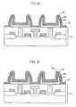
- FIG. 1is a cross sectional view setting forth a semiconductor device in accordance with the present invention.
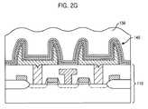
- FIGS. 2A to 2 Gare schematic cross sectional views setting forth a method for the manufacture of the semiconductor memory device in accordance with the present invention.
- FIGS. 1 and 2A to 2 Ga cross sectional view of a semiconductor device 100 for use in a memory cell and cross sectional views setting forth a method for the manufacture thereof in accordance with preferred embodiments of the present invention. It should be noted that like parts appearing in FIGS. 1 and 2A to 2 G are represented by like reference numerals.
- FIG. 1there is provided a cross sectional view of the inventive semiconductor device 100 comprising an active matrix and capacitor structures.
- the active matrixincludes a silicon substrate 102 , transistors formed on top of the silicon substrate 102 , an isolation region 104 for isolating the transistors, poly plugs 116 , a bit line 118 and word lines 120 .
- Each of the transistorshas diffusion regions 106 , a gate oxide 108 , a gate line 112 and a sidewall 114 .
- the bit line 118is electrically connected to one of the diffusion regions 106 to apply an electric potential.
- Each of the capacitor structuresis electrically connected to the other diffusion regions 106 through the poly plugs 116 .
- the bit line 118actually extends in right and left directions bypassing the poly plugs 116 , the drawing does not show these parts of the bit line 118 .
- the capacitor structurescan be connected to a plate line (not shown) to apply thereto a common constant potential.
- Each of the capacitor structuresincludes lower electrodes 125 , diffusion barriers 126 formed on top of the lower electrodes 125 , capacitor dielectrics 128 , composite films 130 and upper electrodes 132 formed on the composite films 130 .
- the capacitor dielectrics 128are disposed between the diffusion barriers 126 and the composite films 130 .
- the lower electrodes 125are made of a poly-Si and the upper electrodes 132 are made of a doped poly-Si with phosphine (PH 3 ) in such a way that its concentration ranges from approximately 1*10 20 to 5*10 20 .
- the composite films 130are made of Ta 2x Al 2(1-x) O y by using an atomic layer deposition (ALD).
- the capacitor dielectrics 128are made of Ta 2 O 5 and the diffusion barriers 126 are made of Si 3 N 4 for preventing diffusions between the lower electrodes 125 and the capacitor dielectrics 128 .
- FIGS. 2A to 2 Gare schematic cross sectional views setting forth the method for manufacture of a capacitor structure 140 for use in a semiconductor memory device in accordance with the present invention.
- the process for manufacturing the semiconductor devicebegins with the preparation of an active matrix 110 including a silicon substrate 102 , an isolation region 104 , diffusion regions 106 , gate oxides 108 , gate lines 112 , a sidewall 114 , a bit line 118 , poly plugs 116 and an insulating layer 122 , as shown in FIG. 2A.
- the bit line 118is electrically connected to one of the diffusion regions 106 to apply an electric potential.
- Each of the poly plugs 116is electrically connected to the other diffusion regions 106 , respectively.
- the capacitor structures 140can be connected to a plate line (not shown) to apply thereto a common constant potential.
- the insulating layer 122is made of a material, e.g., boron-phosphor-silicate glass (BPSG).
- lower electrodes 125are formed on top of the active matrix 110 by using a semiconductor process in such a way that each of the lower electrodes 125 is electrically connected to a corresponding poly plug 116 , as shown in FIG. 1B. It is preferable that the lower electrodes 125 are made of a poly-Si.
- diffusion barriers 126e.g., made of Si 3 N 4 , are formed on the lower electrodes 125 by using a rapid thermal nitrization (RTN) at a temperature ranging from approximately 750° C. to approximately 900° C. as shown in FIG. 2C.
- RTNrapid thermal nitrization
- a capacitor dielectric layer 128is formed on the diffusion barriers 126 and portions of the active matrix 110 , which are not covered with the diffusion barriers 126 , as shown in FIG. 2D.
- the capacitor dielectric layer 128is made of a high K dielectric material such as Ta 2 O 5 by using an atomic layer deposition (ALD).
- ALDatomic layer deposition
- the ALDis carried out at a temperature ranging from approximately 200° C. to approximately 400° C. and at a pressure ranging from approximately 50 mTorr to approximately 250 mTorr.
- the capacitor dielectric layer 128has a thickness ranging from approximately 60 ⁇ to approximately 150 ⁇ .
- the capacitor dielectric layer 128may be performed a surface treatment at a temperature ranging from approximately 200° C. to approximately 400° C.
- a reaction gasis selected from a group consisting Of O 2 , N 2 , N 2 O or the like. It is possible that the surface treatment is carried out by using UV ozone at a temperature ranging from approximately 350° C. to approximately 450° C.
- a composite layer 130is formed on the capacitor dielectric layer 128 by using ADL, as shown in FIG. 2E. It is preferably that the composite layer 130 is made of Ta 2x Al 2(1-x) O y , wherein x and y represents mole %. In the preferred embodiment, x is approximately equal to 0-1 and y is approximately equal to 3-5.
- the composite layer of of Ta 2x Al 2(1-x) O ycan be formed by as follows:
- a reactive gasis selected from a group consisting of O 2 gas, a N 2 O gas, N 2 gas or the like.
- the reaction chamberis maintained at a temperature ranging from approximately 200° C. to approximately 250° C. at a pressure ranging from approximately 50 mTorr to approximately 250 mTorr.
- the Ta 2x Al 2(1-X) O y composite layer 130is densified by heat-treating at a temperature ranging from approximately 650° C. to approximately 850° C. It is preferable that the predefined period of time is between approximately 0.1 seconds and approximately 20 seconds.
- the step d6)is carried out by using UV ozone at a temperature ranging from approximately 350° C. to approximately 450° C.
- the step d6)is carried out by using a plasma process at a temperature ranging from approximately 350° C. to approximately 450° C.
- the Ta 2x Al 2(1-x) O y composite layer 130has a thickness ranging from approximately 10 ⁇ to 30 ⁇ .
- cycles of step d1) to step d4)are controlled in such a way that x is approximately equal to 0-1 and y is approximately equal to 3-5.
- a conductive layer 132is formed on top of the Ta 2x Al 2(1-x) O y composite layer 130 at a temperature ranging from approximately 500° C. to approximately 620° C., as shown in FIG. 2F.
- the conductive layer 132has a thickness ranging from approximately 500 ⁇ to approximately 1,500 ⁇ . It is preferable that the conductive layer 132 is a poly-Si doped with PH 3 in such a way that its concentration ranges from approximately 1*10 20 to 5*10 20 .
- the conductive layer 132 , the Ta 2x Al 2(1-x) O y composite layer 130 and the capacitor dielectric layer 128are patterned into a memory block (not shown).
- an insulating layer 150e.g., made of BPSG, is formed on top of the conductive layer 132 by using a method such as a plasma CVD and made flat by using a method such as chemical mechanical polishing (CMP), as shown in FIG. 2G.
- CMPchemical mechanical polishing
Landscapes
- Semiconductor Memories (AREA)
- Formation Of Insulating Films (AREA)
- Semiconductor Integrated Circuits (AREA)
Abstract
Description
- The present invention relates to a semiconductor device; and, more particularly, to a semiconductor memory device incorporating therein high K dielectric as a capacitor dielectric film.[0001]
- As is well known, a dynamic random access memory (DRAM) with at least one memory cell comprised of a transistor and a capacitor has a higher degree of integration mainly by downsizing through micronization. However, there is still a demand for downsizing the area of the memory cell.[0002]
- To meet the demand, there have been proposed several structures for the capacitor, such as a trench type or a stack type capacitor, which are arranged three-dimensionally in a memory device to reduce the cell area available to the capacitor. However, the process of manufacturing three-dimensionally arranged capacitor is a long and tedious one and consequently involves high manufacturing cost. Therefore, there is a strong demand for a new memory device that can reduce the cell area with securing a requisite volume of information without requiring complex manufacturing steps.[0003]
- In attempt to meet the demand, there have been introduced a high K dielectric, e.g., Ta[0004]2O5or the like, as a capacitor thin film in place of conventional silicon oxide film and/or silicon nitride film. Since, however, a Ta2O5layer is grown with a columnar structure, the grown Ta2O5layer acts also as a high leakage current path. Therefore, it is very difficult for applying the Ta2O5layer to a capacitor thin film for use in memory device.
- Alternatively, a multi-layer dielectric, e.g., Ta[0005]2O/TiO2or Ta2O/Al2O3, has been proposed to use as a capacitor thin film by using a metal organic chemical deposition (MOCVD) to overcome the above-described problem. However, the MOCVD method makes a foreign material reside in the capacitor thin film. This result enforces the capacitor thin film to be performed a high temperature heat-treatment, which, in turn, generates a defect and a high leakage current in the capacitor thin film.
- There are still demands for developing a high K dielectric having a low leakage current which is compatible with a semiconductor process.[0006]
- It is, therefore, an object of the present invention to provide a semiconductor device incorporating therein a high K dielectric as a capacitor dielectric.[0007]
- It is another object of the present invention to provide a method for manufacturing a semiconductor device incorporating therein a high K dielectric as a capacitor dielectric.[0008]
- In accordance with one aspect of the present invention, there is provided a semiconductor device for use in a memory cell, comprising: an active matrix provided with a semiconductor substrate, a plurality of transistors formed on the semiconductor substrate and conductive plugs electrically connected to the transistors; a number of lower electrodes formed on top of the conductive plugs; Ta[0009]2O5films formed on the lower electrodes; composite films formed on the Ta2O5films; and upper electrodes formed on the composite films.
- In accordance with another aspect of the present invention, there is provided a method for manufacturing a semiconductor device for use in a memory cell, the method comprising the steps of: a) preparing an active matrix provided with at least one transistor, a plurality of conductive plugs electrically connected to the transistors and an insulating layer formed around the conductive plugs; b) forming a first conductive layer on top of the active matrix; c) patterning the first conductive layer a predetermined configuration, thereby obtaining a number of lower electrodes; d) forming a Ta[0010]2O5layer on the lower electrodes; e) forming a Ta2xAl2(1-x)Oycomposite layer on the Ta2O5layer, x and y representing mole %; f) forming a second conductive layer on the Ta2xAl2(1-x)Oycomposite layer; and g) patterning the second conductive layer, the Ta2O5layer and the Ta2xAl2(1-X)Oycomposite layer into a preset configuration, thereby obtaining the semiconductor device.
- The above and other objects and features of the present invention will become apparent from the following description of the preferred embodiments given in conjunction with the accompanying drawings, in which:[0011]
- FIG. 1 is a cross sectional view setting forth a semiconductor device in accordance with the present invention; and[0012]
- FIGS. 2A to[0013]2G are schematic cross sectional views setting forth a method for the manufacture of the semiconductor memory device in accordance with the present invention.
- There are provided in FIGS. 1 and 2A to[0014]2G a cross sectional view of a
semiconductor device 100 for use in a memory cell and cross sectional views setting forth a method for the manufacture thereof in accordance with preferred embodiments of the present invention. It should be noted that like parts appearing in FIGS. 1 and 2A to2G are represented by like reference numerals. - In FIG. 1, there is provided a cross sectional view of the[0015]
inventive semiconductor device 100 comprising an active matrix and capacitor structures. The active matrix includes asilicon substrate 102, transistors formed on top of thesilicon substrate 102, anisolation region 104 for isolating the transistors,poly plugs 116, abit line 118 andword lines 120. Each of the transistors hasdiffusion regions 106, agate oxide 108, agate line 112 and asidewall 114. - In the[0016]
semiconductor device 100, thebit line 118 is electrically connected to one of thediffusion regions 106 to apply an electric potential. Each of the capacitor structures is electrically connected to theother diffusion regions 106 through thepoly plugs 116. Although thebit line 118 actually extends in right and left directions bypassing thepoly plugs 116, the drawing does not show these parts of thebit line 118. The capacitor structures can be connected to a plate line (not shown) to apply thereto a common constant potential. - Each of the capacitor structures includes[0017]
lower electrodes 125,diffusion barriers 126 formed on top of thelower electrodes 125,capacitor dielectrics 128,composite films 130 andupper electrodes 132 formed on thecomposite films 130. Thecapacitor dielectrics 128 are disposed between thediffusion barriers 126 and thecomposite films 130. It is preferable that thelower electrodes 125 are made of a poly-Si and theupper electrodes 132 are made of a doped poly-Si with phosphine (PH3) in such a way that its concentration ranges from approximately 1*1020to 5*1020. And also, thecomposite films 130 are made of Ta2xAl2(1-x)Oyby using an atomic layer deposition (ALD). In the preferred embodiment, thecapacitor dielectrics 128 are made of Ta2O5and thediffusion barriers 126 are made of Si3N4for preventing diffusions between thelower electrodes 125 and thecapacitor dielectrics 128. - FIGS. 2A to[0018]2G are schematic cross sectional views setting forth the method for manufacture of a
capacitor structure 140 for use in a semiconductor memory device in accordance with the present invention. - The process for manufacturing the semiconductor device begins with the preparation of an[0019]
active matrix 110 including asilicon substrate 102, anisolation region 104,diffusion regions 106,gate oxides 108,gate lines 112, asidewall 114, abit line 118,poly plugs 116 and aninsulating layer 122, as shown in FIG. 2A. Thebit line 118 is electrically connected to one of thediffusion regions 106 to apply an electric potential. Each of thepoly plugs 116 is electrically connected to theother diffusion regions 106, respectively. Although thebit line 118 actually extends in right and left directions bypassing thepoly plugs 116, the drawing does not show these parts of thebit line 118. Thecapacitor structures 140 can be connected to a plate line (not shown) to apply thereto a common constant potential. Theinsulating layer 122 is made of a material, e.g., boron-phosphor-silicate glass (BPSG). - In an ensuing step,[0020]
lower electrodes 125 are formed on top of theactive matrix 110 by using a semiconductor process in such a way that each of thelower electrodes 125 is electrically connected to acorresponding poly plug 116, as shown in FIG. 1B. It is preferable that thelower electrodes 125 are made of a poly-Si. - Thereafter,[0021]
diffusion barriers 126, e.g., made of Si3N4, are formed on thelower electrodes 125 by using a rapid thermal nitrization (RTN) at a temperature ranging from approximately 750° C. to approximately 900° C. as shown in FIG. 2C. - In a following step, a capacitor[0022]
dielectric layer 128 is formed on thediffusion barriers 126 and portions of theactive matrix 110, which are not covered with thediffusion barriers 126, as shown in FIG. 2D. In the preferred embodiment, the capacitordielectric layer 128 is made of a high K dielectric material such as Ta2O5by using an atomic layer deposition (ALD). In this step, the ALD is carried out at a temperature ranging from approximately 200° C. to approximately 400° C. and at a pressure ranging from approximately 50 mTorr to approximately 250 mTorr. Preferably, the capacitordielectric layer 128 has a thickness ranging from approximately 60 Å to approximately 150 Å. Optionally, the capacitordielectric layer 128 may be performed a surface treatment at a temperature ranging from approximately 200° C. to approximately 400° C. In the surface treatment, a reaction gas is selected from a group consisting Of O2, N2, N2O or the like. It is possible that the surface treatment is carried out by using UV ozone at a temperature ranging from approximately 350° C. to approximately 450° C. - Thereafter, a[0023]
composite layer 130 is formed on the capacitordielectric layer 128 by using ADL, as shown in FIG. 2E. It is preferably that thecomposite layer 130 is made of Ta2xAl2(1-x)Oy, wherein x and y represents mole %. In the preferred embodiment, x is approximately equal to 0-1 and y is approximately equal to 3-5. The composite layer of of Ta2xAl2(1-x)Oycan be formed by as follows: - d1) flowing PET into a reaction chamber as a Ta source with a predefined period of time;[0024]
- d2) flowing H[0025]2O into the reaction chamber as an oxygen source with a predefined period of time;
- d3) flowing TMA into the reaction chamber as an aluminum source with a predefined period of time;[0026]
- d4) flowing H[0027]2O into the reaction chamber as an oxygen source;
- d5) repeating the steps d1) to d4) by a predetermined number of cycles, thereby obtaining the Ta[0028]2xAl2(1-X)Oy
composite layer 130; and - d6) heating the Ta[0029]2xAl2(1-x)Oy
composite layer 130 at a temperature ranging from approximately 650° C. to approximately 850° C. - In the preferred embodiment, during the step d6) a reactive gas is selected from a group consisting of O[0030]2gas, a N2O gas, N2gas or the like. The reaction chamber is maintained at a temperature ranging from approximately 200° C. to approximately 250° C. at a pressure ranging from approximately 50 mTorr to approximately 250 mTorr. Optionally, the Ta2xAl2(1-X)Oy
composite layer 130 is densified by heat-treating at a temperature ranging from approximately 650° C. to approximately 850° C. It is preferable that the predefined period of time is between approximately 0.1 seconds and approximately 20 seconds. - It is possible that the step d6) is carried out by using UV ozone at a temperature ranging from approximately 350° C. to approximately 450° C. Alternatively, the step d6) is carried out by using a plasma process at a temperature ranging from approximately 350° C. to approximately 450° C. Preferably, the Ta[0031]2xAl2(1-x)Oy
composite layer 130 has a thickness ranging from approximately 10 Å to 30 Å. In accordance with preferred embodiment, cycles of step d1) to step d4) are controlled in such a way that x is approximately equal to 0-1 and y is approximately equal to 3-5. - And then, a[0032]
conductive layer 132 is formed on top of the Ta2xAl2(1-x)Oycomposite layer 130 at a temperature ranging from approximately 500° C. to approximately 620° C., as shown in FIG. 2F. Theconductive layer 132 has a thickness ranging from approximately 500 Å to approximately 1,500 Å. It is preferable that theconductive layer 132 is a poly-Si doped with PH3in such a way that its concentration ranges from approximately 1*1020to 5*1020. - In the next step, the[0033]
conductive layer 132, the Ta2xAl2(1-x)Oycomposite layer 130 and thecapacitor dielectric layer 128 are patterned into a memory block (not shown). - Finally, an insulating[0034]
layer 150, e.g., made of BPSG, is formed on top of theconductive layer 132 by using a method such as a plasma CVD and made flat by using a method such as chemical mechanical polishing (CMP), as shown in FIG. 2G. - While the present invention has been described with respect to the particular embodiments, it will be apparent to those skilled in the art that various changes and modifications may be made without departing from the scope of the invention as defined in the following claims.[0035]
Claims (21)
1. A semiconductor device for use in a memory cell, comprising:
an active matrix provided with a semiconductor substrate, a plurality of transistors formed on the semiconductor substrate and conductive plugs electrically connected to the transistors;
a number of lower electrodes formed on top of the conductive plugs;
Ta2O5films formed on the lower electrodes;
composite films formed on the Ta2O5films; and
upper electrodes formed on the composite films.
2. The semiconductor device of
claim 1
3. The semiconductor device of
claim 2
4. The semiconductor device of
claim 3
5. The semiconductor device of
claim 4
6. A method for manufacturing a semiconductor device for use in a memory cell, the method comprising the steps of:
a) preparing an active matrix provided with at least one transistor, a plurality of conductive plugs electrically connected to the transistors and an insulating layer formed around the conductive plugs;
b) forming a first conductive layer on top of the active matrix;
c) patterning the first conductive layer a predetermined configuration, thereby obtaining a number of lower electrodes;
d) forming a Ta2O5layer on the lower electrodes;
e) forming a Ta2xAl2(1-x)Oycomposite layer on the Ta2O5layer, x and y representing mole %;
f) forming a second conductive layer on the Ta2xAl2(1-x)Oycomposite layer; and
g) patterning the second conductive layer, the Ta2O5layer and the Ta2xAl2(1-x)Oycomposite layer into a preset configuration, thereby obtaining the semiconductor device.
7. The method of
claim 6
8. The method of
claim 6
d1) flowing PET into a reaction chamber as a Ta source with a predefined period of time;
d2) flowing H2O into the reaction chamber as an oxygen source with a predefined period of time;
d3) flowing TMA into the reaction chamber as an aluminum source with a predefined period of time;
d4) flowing H2O into the reaction chamber as an oxygen source with a predefined period of time;
d5) repeating the steps d1) to d3) with a predetermined number of cycles, thereby obtaining the Ta2xAl2(1-x)Oycomposite layer; and
d6) heating the Ta2xAl2(1-x)Oycomposite layer at a temperature ranging from approximately 650° C. to approximately 850° C.
9. The method of
claim 8
10. The method of
claim 8
11. The method of
claim 10
12. The method of
claim 8
13. The method of
claim 8
14. The method of
claim 13
15. The method of
claim 8
16. The method of
claim 8
17. The method of
claim 8
18. The method of
claim 16
19. The method of
claim 18
20. The method of
claim 19
21. The method of
claim 20
Priority Applications (1)
| Application Number | Priority Date | Filing Date | Title |
|---|---|---|---|
| US10/269,997US6633062B2 (en) | 1999-12-22 | 2002-10-15 | Semiconductor device incorporated therein high K capacitor dielectric and method for the manufacture thereof |
Applications Claiming Priority (3)
| Application Number | Priority Date | Filing Date | Title |
|---|---|---|---|
| KR99-60534 | 1999-12-22 | ||
| KR1019990060534AKR100624903B1 (en) | 1999-12-22 | 1999-12-22 | Capacitor Manufacturing Method of Semiconductor Device |
| KR1999-60534 | 1999-12-22 |
Related Child Applications (1)
| Application Number | Title | Priority Date | Filing Date |
|---|---|---|---|
| US10/269,997DivisionUS6633062B2 (en) | 1999-12-22 | 2002-10-15 | Semiconductor device incorporated therein high K capacitor dielectric and method for the manufacture thereof |
Publications (2)
| Publication Number | Publication Date |
|---|---|
| US20010025979A1true US20010025979A1 (en) | 2001-10-04 |
| US6486021B2 US6486021B2 (en) | 2002-11-26 |
Family
ID=19628257
Family Applications (2)
| Application Number | Title | Priority Date | Filing Date |
|---|---|---|---|
| US09/727,584Expired - LifetimeUS6486021B2 (en) | 1999-12-22 | 2000-12-04 | Method for manufacturing a semiconductor device having incorporated therein a high K capacitor dielectric |
| US10/269,997Expired - LifetimeUS6633062B2 (en) | 1999-12-22 | 2002-10-15 | Semiconductor device incorporated therein high K capacitor dielectric and method for the manufacture thereof |
Family Applications After (1)
| Application Number | Title | Priority Date | Filing Date |
|---|---|---|---|
| US10/269,997Expired - LifetimeUS6633062B2 (en) | 1999-12-22 | 2002-10-15 | Semiconductor device incorporated therein high K capacitor dielectric and method for the manufacture thereof |
Country Status (4)
| Country | Link |
|---|---|
| US (2) | US6486021B2 (en) |
| JP (1) | JP4671207B2 (en) |
| KR (1) | KR100624903B1 (en) |
| TW (1) | TW478092B (en) |
Cited By (61)
| Publication number | Priority date | Publication date | Assignee | Title |
|---|---|---|---|---|
| US20030190497A1 (en)* | 2002-04-08 | 2003-10-09 | Applied Materials, Inc. | Cyclical deposition of a variable content titanium silicon nitride layer |
| US6638810B2 (en) | 2000-02-22 | 2003-10-28 | Applied Materials, Inc. | Tantalum nitride CVD deposition by tantalum oxide densification |
| US20030224578A1 (en)* | 2001-12-21 | 2003-12-04 | Hua Chung | Selective deposition of a barrier layer on a dielectric material |
| US20030232497A1 (en)* | 2002-04-16 | 2003-12-18 | Ming Xi | System and method for forming an integrated barrier layer |
| US6718126B2 (en) | 2001-09-14 | 2004-04-06 | Applied Materials, Inc. | Apparatus and method for vaporizing solid precursor for CVD or atomic layer deposition |
| US20040067641A1 (en)* | 2002-10-02 | 2004-04-08 | Applied Materials, Inc. | Gas distribution system for cyclical layer deposition |
| US20040077183A1 (en)* | 2002-06-04 | 2004-04-22 | Hua Chung | Titanium tantalum nitride silicide layer |
| US6753248B1 (en) | 2003-01-27 | 2004-06-22 | Applied Materials, Inc. | Post metal barrier/adhesion film |
| US6772072B2 (en) | 2002-07-22 | 2004-08-03 | Applied Materials, Inc. | Method and apparatus for monitoring solid precursor delivery |
| US6773507B2 (en) | 2001-12-06 | 2004-08-10 | Applied Materials, Inc. | Apparatus and method for fast-cycle atomic layer deposition |
| US6831004B2 (en) | 2000-06-27 | 2004-12-14 | Applied Materials, Inc. | Formation of boride barrier layers using chemisorption techniques |
| US6838125B2 (en) | 2002-07-10 | 2005-01-04 | Applied Materials, Inc. | Method of film deposition using activated precursor gases |
| US6846516B2 (en) | 2002-04-08 | 2005-01-25 | Applied Materials, Inc. | Multiple precursor cyclical deposition system |
| US20050067103A1 (en)* | 2003-09-26 | 2005-03-31 | Applied Materials, Inc. | Interferometer endpoint monitoring device |
| US6915592B2 (en) | 2002-07-29 | 2005-07-12 | Applied Materials, Inc. | Method and apparatus for generating gas to a processing chamber |
| US6916398B2 (en) | 2001-10-26 | 2005-07-12 | Applied Materials, Inc. | Gas delivery apparatus and method for atomic layer deposition |
| US6955211B2 (en) | 2002-07-17 | 2005-10-18 | Applied Materials, Inc. | Method and apparatus for gas temperature control in a semiconductor processing system |
| US6972267B2 (en) | 2002-03-04 | 2005-12-06 | Applied Materials, Inc. | Sequential deposition of tantalum nitride using a tantalum-containing precursor and a nitrogen-containing precursor |
| US20050287806A1 (en)* | 2004-06-24 | 2005-12-29 | Hiroyuki Matsuura | Vertical CVD apparatus and CVD method using the same |
| US6998014B2 (en) | 2002-01-26 | 2006-02-14 | Applied Materials, Inc. | Apparatus and method for plasma assisted deposition |
| US7049226B2 (en) | 2001-09-26 | 2006-05-23 | Applied Materials, Inc. | Integration of ALD tantalum nitride for copper metallization |
| US7066194B2 (en) | 2002-07-19 | 2006-06-27 | Applied Materials, Inc. | Valve design and configuration for fast delivery system |
| US7081271B2 (en) | 2001-12-07 | 2006-07-25 | Applied Materials, Inc. | Cyclical deposition of refractory metal silicon nitride |
| US7094685B2 (en) | 2002-01-26 | 2006-08-22 | Applied Materials, Inc. | Integration of titanium and titanium nitride layers |
| US7204886B2 (en) | 2002-11-14 | 2007-04-17 | Applied Materials, Inc. | Apparatus and method for hybrid chemical processing |
| US7211508B2 (en) | 2003-06-18 | 2007-05-01 | Applied Materials, Inc. | Atomic layer deposition of tantalum based barrier materials |
| US7220673B2 (en) | 2000-06-28 | 2007-05-22 | Applied Materials, Inc. | Method for depositing tungsten-containing layers by vapor deposition techniques |
| US7241686B2 (en) | 2004-07-20 | 2007-07-10 | Applied Materials, Inc. | Atomic layer deposition of tantalum-containing materials using the tantalum precursor TAIMATA |
| US7244683B2 (en) | 2003-01-07 | 2007-07-17 | Applied Materials, Inc. | Integration of ALD/CVD barriers with porous low k materials |
| US7262133B2 (en) | 2003-01-07 | 2007-08-28 | Applied Materials, Inc. | Enhancement of copper line reliability using thin ALD tan film to cap the copper line |
| US7352048B2 (en) | 2001-09-26 | 2008-04-01 | Applied Materials, Inc. | Integration of barrier layer and seed layer |
| US20080142866A1 (en)* | 2004-09-08 | 2008-06-19 | Samsung Electronics Co., Ltd. | Integrated Circuit Memory Devices and Capacitors Having Carbon Nanotube Electrodes |
| US7416979B2 (en) | 2001-07-25 | 2008-08-26 | Applied Materials, Inc. | Deposition methods for barrier and tungsten materials |
| US7429516B2 (en) | 2002-02-26 | 2008-09-30 | Applied Materials, Inc. | Tungsten nitride atomic layer deposition processes |
| US7429402B2 (en) | 2004-12-10 | 2008-09-30 | Applied Materials, Inc. | Ruthenium as an underlayer for tungsten film deposition |
| US7429361B2 (en) | 2002-07-17 | 2008-09-30 | Applied Materials, Inc. | Method and apparatus for providing precursor gas to a processing chamber |
| US7465666B2 (en) | 2000-06-28 | 2008-12-16 | Applied Materials, Inc. | Method for forming tungsten materials during vapor deposition processes |
| US7470611B2 (en) | 1998-10-01 | 2008-12-30 | Applied Materials, Inc. | In situ deposition of a low K dielectric layer, barrier layer, etch stop, and anti-reflective coating for damascene application |
| US7585762B2 (en) | 2007-09-25 | 2009-09-08 | Applied Materials, Inc. | Vapor deposition processes for tantalum carbide nitride materials |
| US7611990B2 (en) | 2001-07-25 | 2009-11-03 | Applied Materials, Inc. | Deposition methods for barrier and tungsten materials |
| US7678298B2 (en) | 2007-09-25 | 2010-03-16 | Applied Materials, Inc. | Tantalum carbide nitride materials by vapor deposition processes |
| US7682946B2 (en) | 2005-11-04 | 2010-03-23 | Applied Materials, Inc. | Apparatus and process for plasma-enhanced atomic layer deposition |
| US7745333B2 (en) | 2000-06-28 | 2010-06-29 | Applied Materials, Inc. | Methods for depositing tungsten layers employing atomic layer deposition techniques |
| US7780785B2 (en) | 2001-10-26 | 2010-08-24 | Applied Materials, Inc. | Gas delivery apparatus for atomic layer deposition |
| US7794544B2 (en) | 2004-05-12 | 2010-09-14 | Applied Materials, Inc. | Control of gas flow and delivery to suppress the formation of particles in an MOCVD/ALD system |
| US7798096B2 (en) | 2006-05-05 | 2010-09-21 | Applied Materials, Inc. | Plasma, UV and ion/neutral assisted ALD or CVD in a batch tool |
| US7824743B2 (en) | 2007-09-28 | 2010-11-02 | Applied Materials, Inc. | Deposition processes for titanium nitride barrier and aluminum |
| US8092695B2 (en) | 2006-10-30 | 2012-01-10 | Applied Materials, Inc. | Endpoint detection for photomask etching |
| US8110489B2 (en) | 2001-07-25 | 2012-02-07 | Applied Materials, Inc. | Process for forming cobalt-containing materials |
| US8146896B2 (en) | 2008-10-31 | 2012-04-03 | Applied Materials, Inc. | Chemical precursor ampoule for vapor deposition processes |
| US8187970B2 (en) | 2001-07-25 | 2012-05-29 | Applied Materials, Inc. | Process for forming cobalt and cobalt silicide materials in tungsten contact applications |
| US8323754B2 (en) | 2004-05-21 | 2012-12-04 | Applied Materials, Inc. | Stabilization of high-k dielectric materials |
| US8491967B2 (en) | 2008-09-08 | 2013-07-23 | Applied Materials, Inc. | In-situ chamber treatment and deposition process |
| US8778574B2 (en) | 2012-11-30 | 2014-07-15 | Applied Materials, Inc. | Method for etching EUV material layers utilized to form a photomask |
| US8778204B2 (en) | 2010-10-29 | 2014-07-15 | Applied Materials, Inc. | Methods for reducing photoresist interference when monitoring a target layer in a plasma process |
| US8808559B2 (en) | 2011-11-22 | 2014-08-19 | Applied Materials, Inc. | Etch rate detection for reflective multi-material layers etching |
| US8900469B2 (en) | 2011-12-19 | 2014-12-02 | Applied Materials, Inc. | Etch rate detection for anti-reflective coating layer and absorber layer etching |
| US8961804B2 (en) | 2011-10-25 | 2015-02-24 | Applied Materials, Inc. | Etch rate detection for photomask etching |
| US9051641B2 (en) | 2001-07-25 | 2015-06-09 | Applied Materials, Inc. | Cobalt deposition on barrier surfaces |
| US9418890B2 (en) | 2008-09-08 | 2016-08-16 | Applied Materials, Inc. | Method for tuning a deposition rate during an atomic layer deposition process |
| US9805939B2 (en) | 2012-10-12 | 2017-10-31 | Applied Materials, Inc. | Dual endpoint detection for advanced phase shift and binary photomasks |
Families Citing this family (10)
| Publication number | Priority date | Publication date | Assignee | Title |
|---|---|---|---|---|
| KR100663341B1 (en)* | 2000-08-11 | 2007-01-02 | 삼성전자주식회사 | Atomic Layer Deposition Capacitor Manufacturing Method and Apparatus |
| JP4282245B2 (en)* | 2001-01-31 | 2009-06-17 | 富士通株式会社 | Capacitor element, manufacturing method thereof, and semiconductor device |
| KR100431743B1 (en)* | 2001-12-19 | 2004-05-17 | 주식회사 하이닉스반도체 | Method for forming titanium-nitride layer by atomic layer deposition and method for fabricating capacitor using the same |
| KR20030085822A (en)* | 2002-05-02 | 2003-11-07 | 주성엔지니어링(주) | Method of fabricating capacitor for use in semiconductor device |
| US7060557B1 (en)* | 2002-07-05 | 2006-06-13 | Newport Fab, Llc, Inc. | Fabrication of high-density capacitors for mixed signal/RF circuits |
| US6808983B2 (en)* | 2002-08-27 | 2004-10-26 | Micron Technology, Inc. | Silicon nanocrystal capacitor and process for forming same |
| WO2004105070A2 (en)* | 2003-05-15 | 2004-12-02 | Osram Sylvania Inc. | Vuv-excited device with blue-emitting phosphor |
| KR20050007496A (en)* | 2003-07-08 | 2005-01-19 | 삼성전자주식회사 | Method for forming multi-layer using atomic layer deposition and method for forming capacitor of semiconductor device |
| US7285312B2 (en)* | 2004-01-16 | 2007-10-23 | Honeywell International, Inc. | Atomic layer deposition for turbine components |
| KR100593746B1 (en)* | 2004-12-24 | 2006-06-28 | 삼성전자주식회사 | DRAM capacitors and their formation methods |
Family Cites Families (20)
| Publication number | Priority date | Publication date | Assignee | Title |
|---|---|---|---|---|
| JPS61156865A (en)* | 1984-12-28 | 1986-07-16 | Nec Corp | Semiconductor device |
| JPH03157965A (en)* | 1989-11-15 | 1991-07-05 | Nec Corp | Semiconductor device |
| KR930012120B1 (en)* | 1991-07-03 | 1993-12-24 | 삼성전자 주식회사 | Semiconductor device and manufacturing method thereof |
| JPH05110024A (en)* | 1991-10-18 | 1993-04-30 | Sharp Corp | Semiconductor device and manufacture thereof |
| JPH0677402A (en)* | 1992-07-02 | 1994-03-18 | Natl Semiconductor Corp <Ns> | Dielectric structure for semiconductor device and manufacturing method thereof |
| JPH0766369A (en)* | 1993-08-26 | 1995-03-10 | Nec Corp | Method for manufacturing semiconductor device |
| JPH07263574A (en)* | 1994-03-24 | 1995-10-13 | Oki Electric Ind Co Ltd | Semiconductor device |
| JPH07263573A (en)* | 1994-03-24 | 1995-10-13 | Oki Electric Ind Co Ltd | Semiconductor device and manufacture thereof |
| JPH0951074A (en)* | 1995-08-08 | 1997-02-18 | Sony Corp | Semiconductor device with capacitor |
| JPH10229080A (en)* | 1996-12-10 | 1998-08-25 | Sony Corp | Processing method of oxide, deposition method of amorphous oxide film and amorphous tantalun oxide film |
| US5879459A (en)* | 1997-08-29 | 1999-03-09 | Genus, Inc. | Vertically-stacked process reactor and cluster tool system for atomic layer deposition |
| US5977582A (en)* | 1997-05-23 | 1999-11-02 | Lucent Technologies Inc. | Capacitor comprising improved TaOx -based dielectric |
| KR100269306B1 (en)* | 1997-07-31 | 2000-10-16 | 윤종용 | Integrate circuit device having buffer layer containing metal oxide stabilized by low temperature treatment and fabricating method thereof |
| JPH1174478A (en)* | 1997-09-01 | 1999-03-16 | Matsushita Electron Corp | Manufacture of dielectric film, semiconductor device, manufacture thereof, and manufacturing device therefor |
| KR100275727B1 (en)* | 1998-01-06 | 2001-01-15 | 윤종용 | Capacitor for semiconductor device & manufacturing method |
| JP4026908B2 (en)* | 1998-01-12 | 2007-12-26 | 沖電気工業株式会社 | Manufacturing method of semiconductor device |
| US20020009861A1 (en)* | 1998-06-12 | 2002-01-24 | Pravin K. Narwankar | Method and apparatus for the formation of dielectric layers |
| KR100549566B1 (en)* | 1998-10-29 | 2007-12-21 | 주식회사 하이닉스반도체 | Capacitor Formation Method of Semiconductor Device |
| US6143604A (en)* | 1999-06-04 | 2000-11-07 | Taiwan Semiconductor Manufacturing Company | Method for fabricating small-size two-step contacts for word-line strapping on dynamic random access memory (DRAM) |
| KR100306397B1 (en)* | 1999-12-15 | 2001-10-17 | 김응수 | Continuos deposition method of Al2O3 and Ta2O5 |
- 1999
- 1999-12-22KRKR1019990060534Apatent/KR100624903B1/ennot_activeExpired - Fee Related
- 2000
- 2000-12-04USUS09/727,584patent/US6486021B2/ennot_activeExpired - Lifetime
- 2000-12-18TWTW089127090Apatent/TW478092B/ennot_activeIP Right Cessation
- 2000-12-22JPJP2000391015Apatent/JP4671207B2/ennot_activeExpired - Fee Related
- 2002
- 2002-10-15USUS10/269,997patent/US6633062B2/ennot_activeExpired - Lifetime
Cited By (109)
| Publication number | Priority date | Publication date | Assignee | Title |
|---|---|---|---|---|
| US7470611B2 (en) | 1998-10-01 | 2008-12-30 | Applied Materials, Inc. | In situ deposition of a low K dielectric layer, barrier layer, etch stop, and anti-reflective coating for damascene application |
| US7670945B2 (en) | 1998-10-01 | 2010-03-02 | Applied Materials, Inc. | In situ deposition of a low κ dielectric layer, barrier layer, etch stop, and anti-reflective coating for damascene application |
| US6638810B2 (en) | 2000-02-22 | 2003-10-28 | Applied Materials, Inc. | Tantalum nitride CVD deposition by tantalum oxide densification |
| US7501344B2 (en) | 2000-06-27 | 2009-03-10 | Applied Materials, Inc. | Formation of boride barrier layers using chemisorption techniques |
| US7501343B2 (en) | 2000-06-27 | 2009-03-10 | Applied Materials, Inc. | Formation of boride barrier layers using chemisorption techniques |
| US6831004B2 (en) | 2000-06-27 | 2004-12-14 | Applied Materials, Inc. | Formation of boride barrier layers using chemisorption techniques |
| US7208413B2 (en) | 2000-06-27 | 2007-04-24 | Applied Materials, Inc. | Formation of boride barrier layers using chemisorption techniques |
| US7846840B2 (en) | 2000-06-28 | 2010-12-07 | Applied Materials, Inc. | Method for forming tungsten materials during vapor deposition processes |
| US7674715B2 (en) | 2000-06-28 | 2010-03-09 | Applied Materials, Inc. | Method for forming tungsten materials during vapor deposition processes |
| US7465665B2 (en) | 2000-06-28 | 2008-12-16 | Applied Materials, Inc. | Method for depositing tungsten-containing layers by vapor deposition techniques |
| US7709385B2 (en) | 2000-06-28 | 2010-05-04 | Applied Materials, Inc. | Method for depositing tungsten-containing layers by vapor deposition techniques |
| US7465666B2 (en) | 2000-06-28 | 2008-12-16 | Applied Materials, Inc. | Method for forming tungsten materials during vapor deposition processes |
| US7745333B2 (en) | 2000-06-28 | 2010-06-29 | Applied Materials, Inc. | Methods for depositing tungsten layers employing atomic layer deposition techniques |
| US7220673B2 (en) | 2000-06-28 | 2007-05-22 | Applied Materials, Inc. | Method for depositing tungsten-containing layers by vapor deposition techniques |
| US9209074B2 (en) | 2001-07-25 | 2015-12-08 | Applied Materials, Inc. | Cobalt deposition on barrier surfaces |
| US8110489B2 (en) | 2001-07-25 | 2012-02-07 | Applied Materials, Inc. | Process for forming cobalt-containing materials |
| US7611990B2 (en) | 2001-07-25 | 2009-11-03 | Applied Materials, Inc. | Deposition methods for barrier and tungsten materials |
| US8187970B2 (en) | 2001-07-25 | 2012-05-29 | Applied Materials, Inc. | Process for forming cobalt and cobalt silicide materials in tungsten contact applications |
| US8563424B2 (en) | 2001-07-25 | 2013-10-22 | Applied Materials, Inc. | Process for forming cobalt and cobalt silicide materials in tungsten contact applications |
| US9051641B2 (en) | 2001-07-25 | 2015-06-09 | Applied Materials, Inc. | Cobalt deposition on barrier surfaces |
| US7416979B2 (en) | 2001-07-25 | 2008-08-26 | Applied Materials, Inc. | Deposition methods for barrier and tungsten materials |
| US6718126B2 (en) | 2001-09-14 | 2004-04-06 | Applied Materials, Inc. | Apparatus and method for vaporizing solid precursor for CVD or atomic layer deposition |
| US7494908B2 (en) | 2001-09-26 | 2009-02-24 | Applied Materials, Inc. | Apparatus for integration of barrier layer and seed layer |
| US7352048B2 (en) | 2001-09-26 | 2008-04-01 | Applied Materials, Inc. | Integration of barrier layer and seed layer |
| US7049226B2 (en) | 2001-09-26 | 2006-05-23 | Applied Materials, Inc. | Integration of ALD tantalum nitride for copper metallization |
| US8293328B2 (en) | 2001-10-26 | 2012-10-23 | Applied Materials, Inc. | Enhanced copper growth with ultrathin barrier layer for high performance interconnects |
| US7780785B2 (en) | 2001-10-26 | 2010-08-24 | Applied Materials, Inc. | Gas delivery apparatus for atomic layer deposition |
| US6916398B2 (en) | 2001-10-26 | 2005-07-12 | Applied Materials, Inc. | Gas delivery apparatus and method for atomic layer deposition |
| US7780788B2 (en) | 2001-10-26 | 2010-08-24 | Applied Materials, Inc. | Gas delivery apparatus for atomic layer deposition |
| US8318266B2 (en) | 2001-10-26 | 2012-11-27 | Applied Materials, Inc. | Enhanced copper growth with ultrathin barrier layer for high performance interconnects |
| US8668776B2 (en) | 2001-10-26 | 2014-03-11 | Applied Materials, Inc. | Gas delivery apparatus and method for atomic layer deposition |
| US6773507B2 (en) | 2001-12-06 | 2004-08-10 | Applied Materials, Inc. | Apparatus and method for fast-cycle atomic layer deposition |
| US7081271B2 (en) | 2001-12-07 | 2006-07-25 | Applied Materials, Inc. | Cyclical deposition of refractory metal silicon nitride |
| US7892602B2 (en) | 2001-12-07 | 2011-02-22 | Applied Materials, Inc. | Cyclical deposition of refractory metal silicon nitride |
| US6939801B2 (en) | 2001-12-21 | 2005-09-06 | Applied Materials, Inc. | Selective deposition of a barrier layer on a dielectric material |
| US20030224578A1 (en)* | 2001-12-21 | 2003-12-04 | Hua Chung | Selective deposition of a barrier layer on a dielectric material |
| US7094685B2 (en) | 2002-01-26 | 2006-08-22 | Applied Materials, Inc. | Integration of titanium and titanium nitride layers |
| US7473638B2 (en) | 2002-01-26 | 2009-01-06 | Applied Materials, Inc. | Plasma-enhanced cyclic layer deposition process for barrier layers |
| US7779784B2 (en) | 2002-01-26 | 2010-08-24 | Applied Materials, Inc. | Apparatus and method for plasma assisted deposition |
| US7732325B2 (en) | 2002-01-26 | 2010-06-08 | Applied Materials, Inc. | Plasma-enhanced cyclic layer deposition process for barrier layers |
| US6998014B2 (en) | 2002-01-26 | 2006-02-14 | Applied Materials, Inc. | Apparatus and method for plasma assisted deposition |
| US7745329B2 (en) | 2002-02-26 | 2010-06-29 | Applied Materials, Inc. | Tungsten nitride atomic layer deposition processes |
| US7429516B2 (en) | 2002-02-26 | 2008-09-30 | Applied Materials, Inc. | Tungsten nitride atomic layer deposition processes |
| US7867896B2 (en) | 2002-03-04 | 2011-01-11 | Applied Materials, Inc. | Sequential deposition of tantalum nitride using a tantalum-containing precursor and a nitrogen-containing precursor |
| US6972267B2 (en) | 2002-03-04 | 2005-12-06 | Applied Materials, Inc. | Sequential deposition of tantalum nitride using a tantalum-containing precursor and a nitrogen-containing precursor |
| US7514358B2 (en) | 2002-03-04 | 2009-04-07 | Applied Materials, Inc. | Sequential deposition of tantalum nitride using a tantalum-containing precursor and a nitrogen-containing precursor |
| US20030190497A1 (en)* | 2002-04-08 | 2003-10-09 | Applied Materials, Inc. | Cyclical deposition of a variable content titanium silicon nitride layer |
| US6720027B2 (en) | 2002-04-08 | 2004-04-13 | Applied Materials, Inc. | Cyclical deposition of a variable content titanium silicon nitride layer |
| US6846516B2 (en) | 2002-04-08 | 2005-01-25 | Applied Materials, Inc. | Multiple precursor cyclical deposition system |
| US20030232497A1 (en)* | 2002-04-16 | 2003-12-18 | Ming Xi | System and method for forming an integrated barrier layer |
| US20080014352A1 (en)* | 2002-04-16 | 2008-01-17 | Ming Xi | System and method for forming an integrated barrier layer |
| US7867914B2 (en) | 2002-04-16 | 2011-01-11 | Applied Materials, Inc. | System and method for forming an integrated barrier layer |
| US7279432B2 (en) | 2002-04-16 | 2007-10-09 | Applied Materials, Inc. | System and method for forming an integrated barrier layer |
| US7041335B2 (en) | 2002-06-04 | 2006-05-09 | Applied Materials, Inc. | Titanium tantalum nitride silicide layer |
| US20040077183A1 (en)* | 2002-06-04 | 2004-04-22 | Hua Chung | Titanium tantalum nitride silicide layer |
| US6838125B2 (en) | 2002-07-10 | 2005-01-04 | Applied Materials, Inc. | Method of film deposition using activated precursor gases |
| US7678194B2 (en) | 2002-07-17 | 2010-03-16 | Applied Materials, Inc. | Method for providing gas to a processing chamber |
| US7569191B2 (en) | 2002-07-17 | 2009-08-04 | Applied Materials, Inc. | Method and apparatus for providing precursor gas to a processing chamber |
| US7588736B2 (en) | 2002-07-17 | 2009-09-15 | Applied Materials, Inc. | Apparatus and method for generating a chemical precursor |
| US6955211B2 (en) | 2002-07-17 | 2005-10-18 | Applied Materials, Inc. | Method and apparatus for gas temperature control in a semiconductor processing system |
| US7429361B2 (en) | 2002-07-17 | 2008-09-30 | Applied Materials, Inc. | Method and apparatus for providing precursor gas to a processing chamber |
| US7066194B2 (en) | 2002-07-19 | 2006-06-27 | Applied Materials, Inc. | Valve design and configuration for fast delivery system |
| US7228873B2 (en) | 2002-07-19 | 2007-06-12 | Applied Materials, Inc. | Valve design and configuration for fast delivery system |
| US6772072B2 (en) | 2002-07-22 | 2004-08-03 | Applied Materials, Inc. | Method and apparatus for monitoring solid precursor delivery |
| US7294208B2 (en) | 2002-07-29 | 2007-11-13 | Applied Materials, Inc. | Apparatus for providing gas to a processing chamber |
| US6915592B2 (en) | 2002-07-29 | 2005-07-12 | Applied Materials, Inc. | Method and apparatus for generating gas to a processing chamber |
| US6821563B2 (en) | 2002-10-02 | 2004-11-23 | Applied Materials, Inc. | Gas distribution system for cyclical layer deposition |
| US20040067641A1 (en)* | 2002-10-02 | 2004-04-08 | Applied Materials, Inc. | Gas distribution system for cyclical layer deposition |
| US7591907B2 (en) | 2002-11-14 | 2009-09-22 | Applied Materials, Inc. | Apparatus for hybrid chemical processing |
| US7204886B2 (en) | 2002-11-14 | 2007-04-17 | Applied Materials, Inc. | Apparatus and method for hybrid chemical processing |
| US7402210B2 (en) | 2002-11-14 | 2008-07-22 | Applied Materials, Inc. | Apparatus and method for hybrid chemical processing |
| US7244683B2 (en) | 2003-01-07 | 2007-07-17 | Applied Materials, Inc. | Integration of ALD/CVD barriers with porous low k materials |
| US7262133B2 (en) | 2003-01-07 | 2007-08-28 | Applied Materials, Inc. | Enhancement of copper line reliability using thin ALD tan film to cap the copper line |
| US6753248B1 (en) | 2003-01-27 | 2004-06-22 | Applied Materials, Inc. | Post metal barrier/adhesion film |
| US7211508B2 (en) | 2003-06-18 | 2007-05-01 | Applied Materials, Inc. | Atomic layer deposition of tantalum based barrier materials |
| US7595263B2 (en) | 2003-06-18 | 2009-09-29 | Applied Materials, Inc. | Atomic layer deposition of barrier materials |
| US20050067103A1 (en)* | 2003-09-26 | 2005-03-31 | Applied Materials, Inc. | Interferometer endpoint monitoring device |
| US20070023393A1 (en)* | 2003-09-26 | 2007-02-01 | Nguyen Khiem K | Interferometer endpoint monitoring device |
| US7682984B2 (en) | 2003-09-26 | 2010-03-23 | Applied Materials, Inc. | Interferometer endpoint monitoring device |
| US8282992B2 (en) | 2004-05-12 | 2012-10-09 | Applied Materials, Inc. | Methods for atomic layer deposition of hafnium-containing high-K dielectric materials |
| US8343279B2 (en) | 2004-05-12 | 2013-01-01 | Applied Materials, Inc. | Apparatuses for atomic layer deposition |
| US7794544B2 (en) | 2004-05-12 | 2010-09-14 | Applied Materials, Inc. | Control of gas flow and delivery to suppress the formation of particles in an MOCVD/ALD system |
| US8323754B2 (en) | 2004-05-21 | 2012-12-04 | Applied Materials, Inc. | Stabilization of high-k dielectric materials |
| US20050287806A1 (en)* | 2004-06-24 | 2005-12-29 | Hiroyuki Matsuura | Vertical CVD apparatus and CVD method using the same |
| US7927662B2 (en) | 2004-06-24 | 2011-04-19 | Tokyo Electron Limited | CVD method in vertical CVD apparatus using different reactive gases |
| US20080213478A1 (en)* | 2004-06-24 | 2008-09-04 | Tokyo Electron Limited | Vertical cvd apparatus and cvd method using the same |
| US7691742B2 (en) | 2004-07-20 | 2010-04-06 | Applied Materials, Inc. | Atomic layer deposition of tantalum-containing materials using the tantalum precursor TAIMATA |
| US7241686B2 (en) | 2004-07-20 | 2007-07-10 | Applied Materials, Inc. | Atomic layer deposition of tantalum-containing materials using the tantalum precursor TAIMATA |
| US20080142866A1 (en)* | 2004-09-08 | 2008-06-19 | Samsung Electronics Co., Ltd. | Integrated Circuit Memory Devices and Capacitors Having Carbon Nanotube Electrodes |
| US7429402B2 (en) | 2004-12-10 | 2008-09-30 | Applied Materials, Inc. | Ruthenium as an underlayer for tungsten film deposition |
| US7682946B2 (en) | 2005-11-04 | 2010-03-23 | Applied Materials, Inc. | Apparatus and process for plasma-enhanced atomic layer deposition |
| US7850779B2 (en) | 2005-11-04 | 2010-12-14 | Applied Materisals, Inc. | Apparatus and process for plasma-enhanced atomic layer deposition |
| US9032906B2 (en) | 2005-11-04 | 2015-05-19 | Applied Materials, Inc. | Apparatus and process for plasma-enhanced atomic layer deposition |
| US7798096B2 (en) | 2006-05-05 | 2010-09-21 | Applied Materials, Inc. | Plasma, UV and ion/neutral assisted ALD or CVD in a batch tool |
| US8092695B2 (en) | 2006-10-30 | 2012-01-10 | Applied Materials, Inc. | Endpoint detection for photomask etching |
| US8158526B2 (en) | 2006-10-30 | 2012-04-17 | Applied Materials, Inc. | Endpoint detection for photomask etching |
| US7585762B2 (en) | 2007-09-25 | 2009-09-08 | Applied Materials, Inc. | Vapor deposition processes for tantalum carbide nitride materials |
| US7678298B2 (en) | 2007-09-25 | 2010-03-16 | Applied Materials, Inc. | Tantalum carbide nitride materials by vapor deposition processes |
| US7824743B2 (en) | 2007-09-28 | 2010-11-02 | Applied Materials, Inc. | Deposition processes for titanium nitride barrier and aluminum |
| US8491967B2 (en) | 2008-09-08 | 2013-07-23 | Applied Materials, Inc. | In-situ chamber treatment and deposition process |
| US9418890B2 (en) | 2008-09-08 | 2016-08-16 | Applied Materials, Inc. | Method for tuning a deposition rate during an atomic layer deposition process |
| US8146896B2 (en) | 2008-10-31 | 2012-04-03 | Applied Materials, Inc. | Chemical precursor ampoule for vapor deposition processes |
| US8778204B2 (en) | 2010-10-29 | 2014-07-15 | Applied Materials, Inc. | Methods for reducing photoresist interference when monitoring a target layer in a plasma process |
| US8961804B2 (en) | 2011-10-25 | 2015-02-24 | Applied Materials, Inc. | Etch rate detection for photomask etching |
| US8808559B2 (en) | 2011-11-22 | 2014-08-19 | Applied Materials, Inc. | Etch rate detection for reflective multi-material layers etching |
| US8900469B2 (en) | 2011-12-19 | 2014-12-02 | Applied Materials, Inc. | Etch rate detection for anti-reflective coating layer and absorber layer etching |
| US9805939B2 (en) | 2012-10-12 | 2017-10-31 | Applied Materials, Inc. | Dual endpoint detection for advanced phase shift and binary photomasks |
| US10453696B2 (en) | 2012-10-12 | 2019-10-22 | Applied Materials, Inc. | Dual endpoint detection for advanced phase shift and binary photomasks |
| US8778574B2 (en) | 2012-11-30 | 2014-07-15 | Applied Materials, Inc. | Method for etching EUV material layers utilized to form a photomask |
Also Published As
| Publication number | Publication date |
|---|---|
| US20030040153A1 (en) | 2003-02-27 |
| KR100624903B1 (en) | 2006-09-19 |
| TW478092B (en) | 2002-03-01 |
| US6633062B2 (en) | 2003-10-14 |
| US6486021B2 (en) | 2002-11-26 |
| JP2001230386A (en) | 2001-08-24 |
| JP4671207B2 (en) | 2011-04-13 |
| KR20010063450A (en) | 2001-07-09 |
Similar Documents
| Publication | Publication Date | Title |
|---|---|---|
| US6633062B2 (en) | Semiconductor device incorporated therein high K capacitor dielectric and method for the manufacture thereof | |
| US7012001B2 (en) | Method for manufacturing a semiconductor device for use in a memory cell that includes forming a composite layer of tantalum oxide and titanium oxide over a bottom capacitor electrode | |
| US7157783B2 (en) | Platinum stuffed with silicon oxide as a diffusion oxygen barrier for semiconductor devices | |
| US5702970A (en) | Method for fabricating a capacitor of a semiconductor device | |
| US6642100B2 (en) | Semiconductor device with capacitor structure having hydrogen barrier layer and method for the manufacture thereof | |
| US6627462B1 (en) | Semiconductor device having a capacitor and method for the manufacture thereof | |
| US6475855B1 (en) | Method of forming integrated circuitry, method of forming a capacitor and method of forming DRAM integrated circuitry | |
| US20010001488A1 (en) | Completely encapsulated top electrode of a ferroelectric capacitor using a lead-enhanced encapsulation layer | |
| US20050074980A1 (en) | Method for forming a ruthenium metal layer | |
| US6228701B1 (en) | Apparatus and method for minimizing diffusion in stacked capacitors formed on silicon plugs | |
| US6479364B2 (en) | Method for forming a capacitor for semiconductor devices with diffusion barrier layer on both sides of dielectric layer | |
| US6417101B2 (en) | Method for manufacturing semiconductor memory device incorporating therein copacitor | |
| US6346424B1 (en) | Process for producing high-epsilon dielectric layer or ferroelectric layer | |
| JP3380372B2 (en) | Method for manufacturing semiconductor memory device | |
| US6358789B2 (en) | Method for manufacturing a semiconductor device having a capacitor | |
| CN1954430A (en) | Semiconductor device and process for fabricating same | |
| EP1742269B1 (en) | Semiconductor device and production method therefor | |
| US20010019140A1 (en) | Semiconductor memory device and method for the manufacture thereof | |
| US6465300B2 (en) | Method for forming a lower electrode for use in a semiconductor device | |
| KR0165408B1 (en) | Method for manufacturing capacitor of high dielectric film | |
| US20010046716A1 (en) | Method for manufacturing a semiconductor device | |
| US6437968B1 (en) | Capacitive element | |
| HK1020110A (en) | Polysilicon capacitor electrode |
Legal Events
| Date | Code | Title | Description |
|---|---|---|---|
| AS | Assignment | Owner name:HYUNDAI ELECTRONICS INDUSTRIES CO., LTD., KOREA, R Free format text:ASSIGNMENT OF ASSIGNORS INTEREST;ASSIGNORS:KIM, MIN-SOO;LIM, CHAN;REEL/FRAME:011802/0400 Effective date:20010420 | |
| STCF | Information on status: patent grant | Free format text:PATENTED CASE | |
| FEPP | Fee payment procedure | Free format text:PAYER NUMBER DE-ASSIGNED (ORIGINAL EVENT CODE: RMPN); ENTITY STATUS OF PATENT OWNER: LARGE ENTITY Free format text:PAYOR NUMBER ASSIGNED (ORIGINAL EVENT CODE: ASPN); ENTITY STATUS OF PATENT OWNER: LARGE ENTITY | |
| CC | Certificate of correction | ||
| FPAY | Fee payment | Year of fee payment:4 | |
| FEPP | Fee payment procedure | Free format text:PAYOR NUMBER ASSIGNED (ORIGINAL EVENT CODE: ASPN); ENTITY STATUS OF PATENT OWNER: LARGE ENTITY Free format text:PAYER NUMBER DE-ASSIGNED (ORIGINAL EVENT CODE: RMPN); ENTITY STATUS OF PATENT OWNER: LARGE ENTITY | |
| FPAY | Fee payment | Year of fee payment:8 | |
| FPAY | Fee payment | Year of fee payment:12 |