US20010022362A1 - Thin film semiconductor device and manufacturing method thereof - Google Patents
Thin film semiconductor device and manufacturing method thereofDownload PDFInfo
- Publication number
- US20010022362A1 US20010022362A1US09/808,957US80895701AUS2001022362A1US 20010022362 A1US20010022362 A1US 20010022362A1US 80895701 AUS80895701 AUS 80895701AUS 2001022362 A1US2001022362 A1US 2001022362A1
- Authority
- US
- United States
- Prior art keywords
- substrate
- manufacturing
- thin film
- product substrate
- film transistor
- Prior art date
- Legal status (The legal status is an assumption and is not a legal conclusion. Google has not performed a legal analysis and makes no representation as to the accuracy of the status listed.)
- Granted
Links
Images


Classifications
- H—ELECTRICITY
- H10—SEMICONDUCTOR DEVICES; ELECTRIC SOLID-STATE DEVICES NOT OTHERWISE PROVIDED FOR
- H10D—INORGANIC ELECTRIC SEMICONDUCTOR DEVICES
- H10D30/00—Field-effect transistors [FET]
- H10D30/60—Insulated-gate field-effect transistors [IGFET]
- H10D30/67—Thin-film transistors [TFT]
- H—ELECTRICITY
- H10—SEMICONDUCTOR DEVICES; ELECTRIC SOLID-STATE DEVICES NOT OTHERWISE PROVIDED FOR
- H10D—INORGANIC ELECTRIC SEMICONDUCTOR DEVICES
- H10D86/00—Integrated devices formed in or on insulating or conducting substrates, e.g. formed in silicon-on-insulator [SOI] substrates or on stainless steel or glass substrates
- H10D86/01—Manufacture or treatment
- H10D86/021—Manufacture or treatment of multiple TFTs
- H10D86/0214—Manufacture or treatment of multiple TFTs using temporary substrates
- H—ELECTRICITY
- H10—SEMICONDUCTOR DEVICES; ELECTRIC SOLID-STATE DEVICES NOT OTHERWISE PROVIDED FOR
- H10D—INORGANIC ELECTRIC SEMICONDUCTOR DEVICES
- H10D30/00—Field-effect transistors [FET]
- H10D30/60—Insulated-gate field-effect transistors [IGFET]
- H10D30/67—Thin-film transistors [TFT]
- H10D30/6704—Thin-film transistors [TFT] having supplementary regions or layers in the thin films or in the insulated bulk substrates for controlling properties of the device
- H10D30/6713—Thin-film transistors [TFT] having supplementary regions or layers in the thin films or in the insulated bulk substrates for controlling properties of the device characterised by the properties of the source or drain regions, e.g. compositions or sectional shapes
- H10D30/6715—Thin-film transistors [TFT] having supplementary regions or layers in the thin films or in the insulated bulk substrates for controlling properties of the device characterised by the properties of the source or drain regions, e.g. compositions or sectional shapes characterised by the doping profiles, e.g. having lightly-doped source or drain extensions
- H—ELECTRICITY
- H10—SEMICONDUCTOR DEVICES; ELECTRIC SOLID-STATE DEVICES NOT OTHERWISE PROVIDED FOR
- H10D—INORGANIC ELECTRIC SEMICONDUCTOR DEVICES
- H10D30/00—Field-effect transistors [FET]
- H10D30/60—Insulated-gate field-effect transistors [IGFET]
- H10D30/67—Thin-film transistors [TFT]
- H10D30/6758—Thin-film transistors [TFT] characterised by the insulating substrates
- H—ELECTRICITY
- H10—SEMICONDUCTOR DEVICES; ELECTRIC SOLID-STATE DEVICES NOT OTHERWISE PROVIDED FOR
- H10D—INORGANIC ELECTRIC SEMICONDUCTOR DEVICES
- H10D86/00—Integrated devices formed in or on insulating or conducting substrates, e.g. formed in silicon-on-insulator [SOI] substrates or on stainless steel or glass substrates
- H10D86/40—Integrated devices formed in or on insulating or conducting substrates, e.g. formed in silicon-on-insulator [SOI] substrates or on stainless steel or glass substrates characterised by multiple TFTs
- H10D86/60—Integrated devices formed in or on insulating or conducting substrates, e.g. formed in silicon-on-insulator [SOI] substrates or on stainless steel or glass substrates characterised by multiple TFTs wherein the TFTs are in active matrices
- H—ELECTRICITY
- H10—SEMICONDUCTOR DEVICES; ELECTRIC SOLID-STATE DEVICES NOT OTHERWISE PROVIDED FOR
- H10K—ORGANIC ELECTRIC SOLID-STATE DEVICES
- H10K71/00—Manufacture or treatment specially adapted for the organic devices covered by this subclass
- H—ELECTRICITY
- H10—SEMICONDUCTOR DEVICES; ELECTRIC SOLID-STATE DEVICES NOT OTHERWISE PROVIDED FOR
- H10K—ORGANIC ELECTRIC SOLID-STATE DEVICES
- H10K59/00—Integrated devices, or assemblies of multiple devices, comprising at least one organic light-emitting element covered by group H10K50/00
- H10K59/10—OLED displays
- H10K59/12—Active-matrix OLED [AMOLED] displays
- Y—GENERAL TAGGING OF NEW TECHNOLOGICAL DEVELOPMENTS; GENERAL TAGGING OF CROSS-SECTIONAL TECHNOLOGIES SPANNING OVER SEVERAL SECTIONS OF THE IPC; TECHNICAL SUBJECTS COVERED BY FORMER USPC CROSS-REFERENCE ART COLLECTIONS [XRACs] AND DIGESTS
- Y10—TECHNICAL SUBJECTS COVERED BY FORMER USPC
- Y10S—TECHNICAL SUBJECTS COVERED BY FORMER USPC CROSS-REFERENCE ART COLLECTIONS [XRACs] AND DIGESTS
- Y10S438/00—Semiconductor device manufacturing: process
- Y10S438/977—Thinning or removal of substrate
Definitions
- This inventionrelates to a thin film semiconductor device and a manufacturing method thereof. More specifically, it relates to a constitution of a substrate for integrating and forming a thin film transistor thereon.
- a thin film transistoris integrated and formed on an insulation substrate, for example, made of glass.
- the thin film transistorhas to be formed through steps such as CVD (Chemical Vapor Deposition), cleaning and heat treatment. Since different steps are successively applied, the substrate has to be transported between the stages for each of the processes. If the substrate is deformed such as by warping, automatic transportation using a manipulator is not possible. Therefore, a substrate for use in the thin film semiconductor device requires heat resistance capable of enduring the temperature for forming the thin film transistor. Further, it is necessary for a thickness of a predetermined level or more so as not to cause warping deformation during transportation.
- products using the thin film semiconductor device as a componentcan include, for example, an active matrix type liquid crystal display.
- the thin film semiconductor deviceis required for a structure reduced in weight and of less fracture. Therefore, manufacturing conditions required for the substrate and conditions for the products do not often agree with each other and there is a market complaint against the products.
- use of glass for the substrateis suitable in view of the manufacturing conditions such as heat resistance.
- the glass substratehas a draw back of heavy weight and easy cracking.
- the materialFor the liquid display used in portable electronic equipments such as palm-top computers or portable telephones, it is desirable for the material that the cost is as low as possible, it is reduced in the weight and endurable for some deformation and less cracking upon dropping.
- the glass substrateis heavy, sensitive to deformation and likely to be broken by dropping. That is, there is a difference between restrictions due to manufacturing conditions and preferred characteristics required for the products and it is difficult to satisfy both of the conditions or characteristics and which is left still undissolved.
- this inventionprovides a method of manufacturing a thin film semiconductor device comprising:
- a manufacturing substrate made of an inorganic material and a product substrate made of an organic materialare prepared.
- a moisture proof filmis formed on the surface of a product substrate made of an organic material and then a thin film transistor is formed thereon.
- the manufacturing substrateis bonded to the product substrate by using adhesives coated in the releasable manner.
- this inventionprovides a method of manufacturing a liquid crystal display device comprising:
- this inventionprovides a method of manufacturing an electroluminescence display device comprising:
- a manufacturing substratefor example, made of glass is previously appended to a product substrate, for example, made of a plastic material for reinforcement.
- a thin film transistoris integrated and formed on a product substrate made, for example, of a plastic material.
- the product substrate made, for example, of a plastic material or the likeis backed by the manufacturing substrate made, for example of glass, it has a rigidity as a whole capable of enduring the transportation by manipulators.
- the manufacturing substrate after useis separated from the product substrate.
- the thin film transistoris supported only by a thin and lightweight product substrate.
- An active matrix type liquid crystal display using a plastic substrateis suitable to the application use to the portable equipments.
- FIGS. 1A and 1Bare step charts illustrating a method of manufacturing a thin film semiconductor device according to this invention.
- FIG. 2is a step chart illustrating a method of manufacturing a thin film semiconductor device according to this invention
- FIG. 3is a fragmentary cross sectional view illustrating another embodiment of a thin film semiconductor device according to this invention.
- FIG. 4is a perspective view illustrating a liquid crystal display device according to this invention.
- FIG. 5is a schematic cross sectional view illustrating an electroluminescence display device according to this invention.
- FIGS. 1A and 1Bare an example of schematic step charts illustrating a method of manufacturing a thin film semiconductor device according to this invention.
- a manufacturing substrate 20having characteristics durable to the process for forming a thin film transistor and a product substrate 1 having characteristics suitable to direct mounting of a thin film transistor are prepared.
- a manufacturing substrate 20for example, made of an inorganic material such as glass and a product substrate 1 comprising made of an organic material such as plastic are prepared.
- non-alkali glassis used as the manufacturing substrate 20 .
- the heat resistance of the non-alkali glassis about 500° C.
- the standard thickness for the manufacturing substrate 20is, for example, 0.7 mm. If it is reduced to 0.5 mm, there is no particular problem in view of the manufacturing process. In this embodiment, non-alkali glass is used but, instead, metal plate such as of stainless steel, plastic plate, quartz and the like can be also be used. On the other hand, for the manufacturing substrate 1 , it is necessary to have such a heat resistance as capable of withstanding the processing temperature of a thin film transistor and it is necessary that the substrate is thinner and lighter compared with the manufacturing substrate 20 . In this embodiment, a plastic material is used with a thickness from about 0.1 mm to 0.5 mm.
- polyether sulfone resinPES
- polyethylene terephthalate resin or ARTON resinof excellent heat resistance
- the polyether sulfone resinhas the heat resistance as high as about 250° C.
- the plastic film used for the manufacturing substrate 1may be a single layer and, depending on the case, has a laminate structure.
- a metal platecan be used instead of the plastic material.
- the surfacehas to be insulated.
- the surfacehas to be previously covered with alumina.
- the manufacturing substrate 20is bonded to the product substrate 21 in order to support the product substrate 1 at the back.
- the manufacturing substrate 20is bonded to the product substrate 1 by using an adhesive 21 coated, for example, in a releasable state.
- a heat resistant resinis coated as the adhesive 21 . Since the resin has to endure heat upon forming the thin film transistor, a polyimide, silicon or Teflon type resin is used. However, when the processing temperature for the thin film transistor is lowered, various adhesives can be used. Coating is conducted by spin coating or printing a liquid material.
- the adhesive 21is not restricted only to the organic material but silicon or germanium and, further, metal (lead, aluminum, molybdenum, nickel or tin) may also be used. When such a material is used, it is formed as a film by a sputtering or the like to one of the substrates and bonded to the other of the substrates while being melted under laser irradiation or the like.
- a product substrate 1 made of aluminum or the like and a manufacturing substrate 20 made of glasscan be bonded directly by using an optical energy such as of laser.
- a thin film devicesuch as a thin film transistor 3 is integrated and formed on the surface of the product substrate 1 in a state reinforced with the manufacturing substrate 20 .
- a metalsuch as tantalum or molybdenum
- itis patterned by isotropic dry etching to fabricate into a gate electrode 5 .
- SiO 2is deposited, for example, to a thickness of 100 to 200 nm by a plasma CVD method (PE-CVD method) to form a gate insulation film 4 for covering the gate electrode 5 .
- PE-CVD methodplasma CVD method
- Amorphous siliconis deposited further thereon to a thickness, for example, of 20 to 60 nm to form a semiconductor thin film 2 .
- the insulation film 4 and the semiconductor thin film 2can be grown continuously without breaking vacuum in one identical film forming chamber.
- the semiconductor thin film 2is crystallized, for example, by irradiating an XeCl excimer laser beam at a wavelength of 308 nm for an extremely short period of time.
- the amorphous siliconis melted by the energy of the laser beam and forms polycrystal silicon when solidified. Since the irradiation time of the laser beam is extremely short, it gives no damages to the product substrate 1 .
- resistis coated on the semiconductor thin film 2 and back face exposure is applied by using a light shielding gate electrode 5 as a mask to obtain a mask aligned with the gate electrode 5 in self-alignment.
- impuritiesfor example, phosphorus
- impuritiesare implanted by way of the mask by an ion doping method into the semiconductor thin film 2 at a relatively low concentration.
- impuritiesfor example, phosphorus
- impuritiesare implanted at a relatively high concentration by an ion doping method to the semiconductor thin film 2 .
- a source region S and a drain region Dare thus formed.
- a channel region Ch previously implanted with P-type impurities (for example, boron) for threshold value controlis left just above the gate electrode 5 .
- P-type impuritiesfor example, boron
- an LDD region implanted with N-type impurities such as phosphorus at a relatively low concentrationis left.
- unnecessary photoresistis removed.
- the ion doping methodis a method of doping ions in a plasma state under electric field acceleration all at once into the semiconductor thin film 2 that enables short time processing. Successively, a laser beam is irradiated again for activating the doped atoms.
- SiO 2for example, is deposited to form an interlayer film 9 for insulation between interconnections.
- metal aluminum or the likeis deposited by sputtering, patterned to a predetermined shape and fabricated into interconnections 10 .
- a protection film 12 or a pixel electrode 14is formed optionally.
- an assembling stepis applied by bonding an opposing substrate previously formed with opposing electrodes to the product substrate formed with the pixel electrode 14 at a predetermined distance, and injecting liquid crystals into the gap.
- an organic electroluminescence deviceis previously formed on the pixel electrode 14 .
- a separation step of separating the used manufacturing substrate from the productivity substrate 1is applied.
- both of the substratescan be separated by dissolving adhesives interposed between the manufacturing substrate 20 and the product substrate 1 in a solvent.
- the solvent usedis different depending on the material of the adhesives.
- adhesive layeris extremely thin and takes much time till the solvent intrudes. Then, it is effective to promote the dissolution of the adhesives by using an energy such as of supersonic waves or laser beams. In the previous bonding step, it is not necessary to uniformly coat the adhesive over the entire surface of the substrate. Rather, dissolution using the solvent is facilitated by coating the adhesives discretely.
- the assembling step described abovemay be applied after separation of the manufacturing substrate 20 .
- a thin film transistor of the bottom gate structurehas been formed on the substrate 1 .
- a thin film transistor of a top gate structuremay also be integrated and formed.
- FIG. 3shows this embodiment.
- corresponding reference numeralsare attached to those portions corresponding to the previous embodiment shown in FIG. 1 and FIG. 2.
- the gate electrode 5is formed by way of the gate insulation film 4 on the semiconductor thin film 2 .
- a moisture proof buffer film 30is formed previously between the product substrate 1 and the thin film transistor.
- the buffer film 30comprises a silicon oxide film or a silicon nitride film formed by a CVD or sputtering method, which stops water passing through the manufacturing substrate 1 and suppresses impurities from intruding into the substrate.
- a buffer filmparticularly as a moisture proof countermeasure.
- FIG. 4is a schematic perspective view illustrating an example of an active matrix type liquid crystal display device assembled by using a thin film semiconductor device according to this invention as a driving substrate.
- the liquid crystal display devicehas a panel structure of possessing liquid crystals 50 between a product substrate 1 and an opposed substrate 60 .
- a pixel array area and a peripheral circuit areaare integrated and formed by the same thin film transistor as described above on the product substrate 1 .
- the peripheral circuit areais divided into a vertical scanning circuit 41 and a horizontal scanning circuit 42 .
- terminal electrodes 47 for external connectionare also formed on the upper end of the product substrate 1 . Each of the terminal electrode 47 is connected by way of interconnections 48 to the vertical scanning circuit 41 and the horizontal scanning circuit 42 .
- Gate interconnections 43 and signal interconnections 10 crossing to each otherare formed in the pixel array area.
- the gate electrode 43is connected with the vertical scanning circuit 41 while the signal interconnection 10 is connected with the horizontal scanning circuit 42 .
- a pixel electrode 14 and a thin film transistor 3 for driving the sameare formed at the intersection between both of the interconnections 43 and 10 .
- counter electrodesare formed although not illustrated to the inner surface of the opposing substrate.
- FIG. 5is a schematic fragmentary cross sectional view illustrating an active matrix type electroluminescence display device assembled using a thin film semiconductor device according to this invention as a driving substrate.
- an organic electroluminescence device OLEDis used as a pixel.
- the OLEDcomprises an anode A, an organic layer 110 and a cathode K stacked successively.
- the anode Ais isolated on every pixels and made, for example, of chromium and basically light reflecting.
- the cathode Kis connected in common between each of the pixels, has a laminate structure, for example, of a metal layer 111 and a transparent conduction layer 112 and is basically light permeable.
- a thin film transistor 3 for driving the OLEDcomprises a gate electrode 5 formed on a product substrate 1 made, for example, of a plastic material, a gate insulation film 4 stacked thereon and a semiconductor thin film 2 stacked above the gate electrode 5 by way of the gate insulation film 4 .
- the semiconductor thin film 2comprises, for example, a silicon thin film crystallized by laser annealing.
- the thin film transistor 3comprises a source region S, a channel region Ch and a drain region D as a passage for the current supply to the OLED.
- the channel region Chsituates just above the gate electrode 5 .
- the thin film transistor 3 having the bottom gate structureis covered with an interlayer film 9 , on which interconnections 10 are formed.
- the film of the OLED described aboveis formed on them by way of another interlayer film 11 .
- the anode A of the OLEDis electrically connected by way of the interconnections 10 to the thin film transistor 3 .
- this inventioncomprises a structure in which the manufacturing substrate having a characteristic durable to the process for forming the thin film transistor and the product substrate having a characteristic suitable to direct mounting of the thin film transistor are used, the manufacturing substrate is bonded to the product substrate for supporting the product substrate at the back, at least the thin film transistor is formed on the surface of the product substrate in a state reinforced with the manufacturing substrate, and the manufacturing substrate after use is separated from the product substrate.
- the manufacturing substrate after useis separated in a stage where the product is completed, the product itself is reduced in the weight and the thickness.
- the separated manufacturing substratecan further be utilized again to the thin film transistor manufacturing process, making it possible for recycling of resource.
Landscapes
- Engineering & Computer Science (AREA)
- Manufacturing & Machinery (AREA)
- Thin Film Transistor (AREA)
- Liquid Crystal (AREA)
- Electroluminescent Light Sources (AREA)
- Devices For Indicating Variable Information By Combining Individual Elements (AREA)
Abstract
Description
- 1. Field of the Invention[0001]
- This invention relates to a thin film semiconductor device and a manufacturing method thereof. More specifically, it relates to a constitution of a substrate for integrating and forming a thin film transistor thereon.[0002]
- 2. Description of the Related Art[0003]
- Generally, in a thin film semiconductor device, a thin film transistor is integrated and formed on an insulation substrate, for example, made of glass. The thin film transistor has to be formed through steps such as CVD (Chemical Vapor Deposition), cleaning and heat treatment. Since different steps are successively applied, the substrate has to be transported between the stages for each of the processes. If the substrate is deformed such as by warping, automatic transportation using a manipulator is not possible. Therefore, a substrate for use in the thin film semiconductor device requires heat resistance capable of enduring the temperature for forming the thin film transistor. Further, it is necessary for a thickness of a predetermined level or more so as not to cause warping deformation during transportation.[0004]
- On the other hand, products using the thin film semiconductor device as a component can include, for example, an active matrix type liquid crystal display. When a liquid crystal display is used for portable equipments, the thin film semiconductor device is required for a structure reduced in weight and of less fracture. Therefore, manufacturing conditions required for the substrate and conditions for the products do not often agree with each other and there is a market complaint against the products. As described above, use of glass for the substrate is suitable in view of the manufacturing conditions such as heat resistance. However, in view of the product conditions, the glass substrate has a draw back of heavy weight and easy cracking. For the liquid display used in portable electronic equipments such as palm-top computers or portable telephones, it is desirable for the material that the cost is as low as possible, it is reduced in the weight and endurable for some deformation and less cracking upon dropping. Actually, the glass substrate is heavy, sensitive to deformation and likely to be broken by dropping. That is, there is a difference between restrictions due to manufacturing conditions and preferred characteristics required for the products and it is difficult to satisfy both of the conditions or characteristics and which is left still undissolved.[0005]
- Various countermeasures have been proposed so far in order to overcome such problems. For example, it has been attempted to use a plastic substrate, for example, by lowering the process temperature for the thin film transistor as much as possible. However, the plastic substrate suffers from larger deformation compared with the glass substrate and no satisfactory products are obtained at present (N. D. Young, et al., Euro Display '96 Digest, 555, 1996). Further, there has been proposed a countermeasure of once forming a thin film transistor to a provisional substrate and then transferring the same to another substrate which is disclosed, for example, in Japanese Published Unexamined Patent Application Hei 11-243209. However, this method is complicated in the transfer step and involves a problem in view of the productivity. Further, since the provisional substrate used for forming the thin film transistor and a substrate for mounting the thin film transistor as a product are different, characteristic are liable to be fluctuated in the thin film transistor in view of the problem such as stresses and the like.[0006]
- For overcoming the foregoing problems in the prior art, this invention provides a method of manufacturing a thin film semiconductor device comprising:[0007]
- a preparatory step of preparing a manufacturing substrate having a characteristic capable of enduring a process for forming a thin film transistor and a product substrate having a characteristic suitable to direct mounting of the thin film transistor,[0008]
- a bonding step of bonding the manufacturing substrate to the product substrate for supporting the product substrate at the back,[0009]
- a formation step of forming at least a thin film transistor to the surface of the product substrate in a state reinforced with the manufacturing substrate and[0010]
- a separation step of separating the manufacturing substrate after use from the product substrate.[0011]
- Preferably, in the preparatory step, a manufacturing substrate made of an inorganic material and a product substrate made of an organic material are prepared. Optionally, in the formation step, a moisture proof film is formed on the surface of a product substrate made of an organic material and then a thin film transistor is formed thereon. Further, in the bonding step, the manufacturing substrate is bonded to the product substrate by using adhesives coated in the releasable manner.[0012]
- Further, this invention provides a method of manufacturing a liquid crystal display device comprising:[0013]
- a preparatory step of preparing a manufacturing substrate having a characteristic capable of enduring a process for forming a thin film transistor and a product substrate having a characteristic suitable to direct mounting of the thin film transistor,[0014]
- a bonding step of bonding the manufacturing substrate to the product substrate for supporting the product substrate at the back,[0015]
- a formation step of forming at least a thin film transistor and a pixel electrode to the surface of the product substrate in a state reinforced with the manufacturing substrate,[0016]
- a separation step of separating the manufacturing substrate after use from the product substrate, and[0017]
- an assembling step of joining an opposing substrate previously formed with opposing electrodes at a predetermined distance to the product substrate formed with the pixel electrodes before or after the separation step, and injecting liquid crystals in the gap.[0018]
- Furthermore, this invention provides a method of manufacturing an electroluminescence display device comprising:[0019]
- a preparatory step of preparing a manufacturing substrate having a characteristic capable of enduring a process for forming a thin film transistor and a product substrate having a characteristic suitable to direct mounting of the thin film transistor,[0020]
- a bonding step of bonding the manufacturing substrate to the product substrate for supporting the product substrate at the back,[0021]
- a formation step of forming at least a thin film transistor and an electroluminescence device to the surface of the product substrate in a state reinforced with the manufacturing substrate, and[0022]
- a separation step of separating the manufacturing substrate after use from the product substrate.[0023]
- According to this invention, in the preparatory step before forming the thin film transistor, a manufacturing substrate, for example, made of glass is previously appended to a product substrate, for example, made of a plastic material for reinforcement. Subsequently, a thin film transistor is integrated and formed on a product substrate made, for example, of a plastic material. In this case, since the product substrate made, for example, of a plastic material or the like is backed by the manufacturing substrate made, for example of glass, it has a rigidity as a whole capable of enduring the transportation by manipulators. Then, at the instance the manufacturing process for the thin film transistor has been completed, the manufacturing substrate after use is separated from the product substrate. Finally, the thin film transistor is supported only by a thin and lightweight product substrate. An active matrix type liquid crystal display using a plastic substrate is suitable to the application use to the portable equipments.[0024]
- FIGS. 1A and 1B are step charts illustrating a method of manufacturing a thin film semiconductor device according to this invention;[0025]
- FIG. 2 is a step chart illustrating a method of manufacturing a thin film semiconductor device according to this invention;[0026]
- FIG. 3 is a fragmentary cross sectional view illustrating another embodiment of a thin film semiconductor device according to this invention;[0027]
- FIG. 4 is a perspective view illustrating a liquid crystal display device according to this invention; and[0028]
- FIG. 5 is a schematic cross sectional view illustrating an electroluminescence display device according to this invention.[0029]
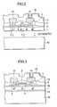
- Preferred embodiments of this invention are to be described in details with reference to the drawings. FIGS. 1A and 1B are an example of schematic step charts illustrating a method of manufacturing a thin film semiconductor device according to this invention. At first, as shown in FIG. 1A, a[0030]
manufacturing substrate 20 having characteristics durable to the process for forming a thin film transistor and aproduct substrate 1 having characteristics suitable to direct mounting of a thin film transistor are prepared. In the preparatory step, amanufacturing substrate 20, for example, made of an inorganic material such as glass and aproduct substrate 1 comprising made of an organic material such as plastic are prepared. In this embodiment, non-alkali glass is used as themanufacturing substrate 20. The heat resistance of the non-alkali glass is about 500° C. The standard thickness for themanufacturing substrate 20 is, for example, 0.7 mm. If it is reduced to 0.5 mm, there is no particular problem in view of the manufacturing process. In this embodiment, non-alkali glass is used but, instead, metal plate such as of stainless steel, plastic plate, quartz and the like can be also be used. On the other hand, for themanufacturing substrate 1, it is necessary to have such a heat resistance as capable of withstanding the processing temperature of a thin film transistor and it is necessary that the substrate is thinner and lighter compared with themanufacturing substrate 20. In this embodiment, a plastic material is used with a thickness from about 0.1 mm to 0.5 mm. Particularly, polyether sulfone resin (PES), polyethylene terephthalate resin or ARTON resin of excellent heat resistance is used. The polyether sulfone resin has the heat resistance as high as about 250° C. The plastic film used for themanufacturing substrate 1 may be a single layer and, depending on the case, has a laminate structure. Particularly, when this is used to a reflection type display not a transmission type display, a metal plate can be used instead of the plastic material. However, when the metal plate is used, the surface has to be insulated. For example, when an aluminum plate is used for theproduct substrate 1, the surface has to be previously covered with alumina. - Successively, as shown in FIG. 1A, the[0031]
manufacturing substrate 20 is bonded to theproduct substrate 21 in order to support theproduct substrate 1 at the back. In the bonding step, themanufacturing substrate 20 is bonded to theproduct substrate 1 by using an adhesive21 coated, for example, in a releasable state. In this embodiment, a heat resistant resin is coated as the adhesive21. Since the resin has to endure heat upon forming the thin film transistor, a polyimide, silicon or Teflon type resin is used. However, when the processing temperature for the thin film transistor is lowered, various adhesives can be used. Coating is conducted by spin coating or printing a liquid material. Instead, there is a method of appending a film-shaped adhesive to one of the substrate surfaces and then coating by heat melting the same. The adhesive21 is not restricted only to the organic material but silicon or germanium and, further, metal (lead, aluminum, molybdenum, nickel or tin) may also be used. When such a material is used, it is formed as a film by a sputtering or the like to one of the substrates and bonded to the other of the substrates while being melted under laser irradiation or the like. In a case of using an aluminum plate as theproduct substrate 1, aproduct substrate 1 made of aluminum or the like and amanufacturing substrate 20 made of glass can be bonded directly by using an optical energy such as of laser. - Successively, as shown in FIG. 1B, a thin film device such as a[0032]
thin film transistor 3 is integrated and formed on the surface of theproduct substrate 1 in a state reinforced with themanufacturing substrate 20. Specifically, after forming film of a metal such as tantalum or molybdenum by a sputtering method or the like at first, it is patterned by isotropic dry etching to fabricate into agate electrode 5. Successively, SiO2is deposited, for example, to a thickness of 100 to 200 nm by a plasma CVD method (PE-CVD method) to form agate insulation film 4 for covering thegate electrode 5. Amorphous silicon is deposited further thereon to a thickness, for example, of 20 to 60 nm to form a semiconductorthin film 2. Theinsulation film 4 and the semiconductorthin film 2 can be grown continuously without breaking vacuum in one identical film forming chamber. Subsequently, the semiconductorthin film 2 is crystallized, for example, by irradiating an XeCl excimer laser beam at a wavelength of 308 nm for an extremely short period of time. The amorphous silicon is melted by the energy of the laser beam and forms polycrystal silicon when solidified. Since the irradiation time of the laser beam is extremely short, it gives no damages to theproduct substrate 1. Subsequently, resist is coated on the semiconductorthin film 2 and back face exposure is applied by using a light shieldinggate electrode 5 as a mask to obtain a mask aligned with thegate electrode 5 in self-alignment. Then, impurities (for example, phosphorus) are implanted by way of the mask by an ion doping method into the semiconductorthin film 2 at a relatively low concentration. Further, after covering the mask and the peripheral thereof with another photoresist, impurities (for example, phosphorus) are implanted at a relatively high concentration by an ion doping method to the semiconductorthin film 2. A source region S and a drain region D are thus formed. Further, a channel region Ch previously implanted with P-type impurities (for example, boron) for threshold value control is left just above thegate electrode 5. Between the channel region Ch, and the source region S or the drain region D, an LDD region implanted with N-type impurities such as phosphorus at a relatively low concentration is left. Subsequently, unnecessary photoresist is removed. The ion doping method is a method of doping ions in a plasma state under electric field acceleration all at once into the semiconductorthin film 2 that enables short time processing. Successively, a laser beam is irradiated again for activating the doped atoms. This is the same method as for crystallization but a weak energy may suffice since there is no requirement for growing the crystals. Then, SiO2, for example, is deposited to form aninterlayer film 9 for insulation between interconnections. After making a contact hole in theinterlayer film 9, metal aluminum or the like is deposited by sputtering, patterned to a predetermined shape and fabricated intointerconnections 10. In the subsequent procedures, in a case of manufacturing a thin film semiconductor device for use in an active matrix type liquid crystal display, aprotection film 12 or apixel electrode 14 is formed optionally. Further, an assembling step is applied by bonding an opposing substrate previously formed with opposing electrodes to the product substrate formed with thepixel electrode 14 at a predetermined distance, and injecting liquid crystals into the gap. On the other hand, in a case of using the thin film semiconductor device for an active matrix type organic electroluminescence display, an organic electroluminescence device is previously formed on thepixel electrode 14. - Finally, as shown in FIG. 2, a separation step of separating the used manufacturing substrate from the[0033]
productivity substrate 1 is applied. Specifically, both of the substrates can be separated by dissolving adhesives interposed between the manufacturingsubstrate 20 and theproduct substrate 1 in a solvent. The solvent used is different depending on the material of the adhesives. Generally, adhesive layer is extremely thin and takes much time till the solvent intrudes. Then, it is effective to promote the dissolution of the adhesives by using an energy such as of supersonic waves or laser beams. In the previous bonding step, it is not necessary to uniformly coat the adhesive over the entire surface of the substrate. Rather, dissolution using the solvent is facilitated by coating the adhesives discretely. As described above, since only theproduct substrate 1 made of the plastic material or the like is left to the final product, a display light in weight and reduced in the thickness can be obtained. In the case of preparing a liquid crystal display, the assembling step described above may be applied after separation of themanufacturing substrate 20. - In the embodiment described above, a thin film transistor of the bottom gate structure has been formed on the[0034]
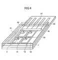
substrate 1. Instead, a thin film transistor of a top gate structure may also be integrated and formed. FIG. 3 shows this embodiment. For easy understanding, corresponding reference numerals are attached to those portions corresponding to the previous embodiment shown in FIG. 1 and FIG. 2. As shown in the drawing, in the thin film transistor of the top gate structure, thegate electrode 5 is formed by way of thegate insulation film 4 on the semiconductorthin film 2. In this embodiment, a moistureproof buffer film 30 is formed previously between theproduct substrate 1 and the thin film transistor. Thebuffer film 30 comprises a silicon oxide film or a silicon nitride film formed by a CVD or sputtering method, which stops water passing through themanufacturing substrate 1 and suppresses impurities from intruding into the substrate. In a case of using a plastic material for theproduct substrate 1, it is sometimes preferred to form a buffer film particularly as a moisture proof countermeasure. - FIG. 4 is a schematic perspective view illustrating an example of an active matrix type liquid crystal display device assembled by using a thin film semiconductor device according to this invention as a driving substrate. The liquid crystal display device has a panel structure of possessing[0035]
liquid crystals 50 between aproduct substrate 1 and anopposed substrate 60. A pixel array area and a peripheral circuit area are integrated and formed by the same thin film transistor as described above on theproduct substrate 1. The peripheral circuit area is divided into avertical scanning circuit 41 and ahorizontal scanning circuit 42. Further,terminal electrodes 47 for external connection are also formed on the upper end of theproduct substrate 1. Each of theterminal electrode 47 is connected by way ofinterconnections 48 to thevertical scanning circuit 41 and thehorizontal scanning circuit 42.Gate interconnections 43 andsignal interconnections 10 crossing to each other are formed in the pixel array area. Thegate electrode 43 is connected with thevertical scanning circuit 41 while thesignal interconnection 10 is connected with thehorizontal scanning circuit 42. Apixel electrode 14 and athin film transistor 3 for driving the same are formed at the intersection between both of theinterconnections product substrate 1 and identical plastic material is used as the opposingsubstrate 60, a panel extremely light in weight and resistant to damages can be obtained. - FIG. 5 is a schematic fragmentary cross sectional view illustrating an active matrix type electroluminescence display device assembled using a thin film semiconductor device according to this invention as a driving substrate. In this embodiment, an organic electroluminescence device OLED is used as a pixel. The OLED comprises an anode A, an[0036]
organic layer 110 and a cathode K stacked successively. The anode A is isolated on every pixels and made, for example, of chromium and basically light reflecting. The cathode K is connected in common between each of the pixels, has a laminate structure, for example, of ametal layer 111 and a transparent conduction layer112 and is basically light permeable. When a forward voltage (at about 10 V) is applied between the anode A and the cathode K of the OLED of such a structure, injection of carriers such as electrons or positive holes occurs and light emission is observed. It is considered that the operation of the OLED is light emission caused by exciters formed with holes injected from the anode A and electrons injected from the cathode K. - On the other hand, a[0037]
thin film transistor 3 for driving the OLED comprises agate electrode 5 formed on aproduct substrate 1 made, for example, of a plastic material, agate insulation film 4 stacked thereon and a semiconductorthin film 2 stacked above thegate electrode 5 by way of thegate insulation film 4. The semiconductorthin film 2 comprises, for example, a silicon thin film crystallized by laser annealing. Thethin film transistor 3 comprises a source region S, a channel region Ch and a drain region D as a passage for the current supply to the OLED. The channel region Ch situates just above thegate electrode 5. Thethin film transistor 3 having the bottom gate structure is covered with aninterlayer film 9, on whichinterconnections 10 are formed. The film of the OLED described above is formed on them by way of anotherinterlayer film 11. The anode A of the OLED is electrically connected by way of theinterconnections 10 to thethin film transistor 3. - As has been described above, this invention comprises a structure in which the manufacturing substrate having a characteristic durable to the process for forming the thin film transistor and the product substrate having a characteristic suitable to direct mounting of the thin film transistor are used, the manufacturing substrate is bonded to the product substrate for supporting the product substrate at the back, at least the thin film transistor is formed on the surface of the product substrate in a state reinforced with the manufacturing substrate, and the manufacturing substrate after use is separated from the product substrate. In the manufacturing steps, since the thin film transistor is integrated and formed on the substrate reinforced with bonding handling for substrate, etc. can be facilitated to contribute to the stabilization of the process. On the other hand, since the manufacturing substrate after use is separated in a stage where the product is completed, the product itself is reduced in the weight and the thickness. In addition, the separated manufacturing substrate can further be utilized again to the thin film transistor manufacturing process, making it possible for recycling of resource.[0038]
Claims (21)
1. A method of manufacturing a thin film semiconductor device comprising:
a preparatory step of preparing a manufacturing substrate having a characteristic capable of enduring a process for forming a thin film transistor and a product substrate having a characteristic suitable to direct mounting of the thin film transistor,
a bonding step of bonding the manufacturing substrate to the product substrate for supporting the product substrate at the back,
a formation step of forming at least a thin film transistor to the surface of the product substrate in a state reinforced with the manufacturing substrate, and
a separation step of separating the manufacturing substrate after use from the product substrate.
2. A method of manufacturing a thin film semiconductor device as claimed in
claim 1
3. A method of manufacturing a thin film semiconductor device as claimed in
claim 2
4. A method of manufacturing a thin film semiconductor device as claimed in
claim 1
5. A method of manufacturing a liquid crystal display device comprising:
a preparatory step of preparing a manufacturing substrate having a characteristic capable of enduring a process for forming a thin film transistor and a product substrate having a characteristic suitable to direct mounting of the thin film transistor,
a bonding step of bonding the manufacturing substrate to the product substrate for supporting the product substrate at the back,
a formation step of forming at least a thin film transistor and a pixel electrode to the surface of the product substrate in a state reinforced with the manufacturing substrate,
a separation step of separating the manufacturing substrate after use from the product substrate, and
an assembling step of joining an opposing substrate previously formed with opposing electrodes at a predetermined distance to the product substrate formed with the pixel electrodes before or after the separation step, and injecting liquid crystals in the gap.
6. A method of manufacturing a liquid crystal display device as claimed in
claim 5
7. A method of manufacturing a liquid crystal display device as claimed in
claim 6
8. A method of manufacturing a liquid crystal display device as claimed in
claim 5
9. A method of manufacturing an electroluminescence display device comprising:
a preparatory step of preparing a manufacturing substrate having a characteristic capable of enduring a process for forming a thin film transistor and a product substrate having a characteristic suitable to direct mounting of the thin film transistor,
a bonding step of bonding the manufacturing substrate to the product substrate for supporting the product substrate at the back,
a formation step of forming at least a thin film transistor and an electroluminescence device to the surface of the product substrate in a state reinforced with the manufacturing substrate, and
a separation step of separating the manufacturing substrate after use from the product substrate.
10. A method of manufacturing an electroluminescence display device as claimed in
claim 9
11. A method of manufacturing an electroluminescence display device as claimed in
claim 10
12. A method of manufacturing an electroluminescence display device as claimed in
claim 9
13. A thin film semiconductor device having a structure formed by using a manufacturing substrate having a characteristic capable of enduring a process for forming a thin film transistor and a product substrate having a characteristic suitable to direct mounting of the thin film transistor, bonding the manufacturing substrate to the product substrate for supporting the product substrate at the back, forming at least a thin film transistor to the surface of the product substrate in a state reinforced with the manufacturing substrate, and separating the manufacturing substrate after use from the product substrate.
14. A thin film semiconductor device as claimed in
claim 13
15. A thin film semiconductor device as claimed in
claim 14
16. A liquid crystal display device having a structure formed by using a manufacturing substrate having a characteristic capable of enduring the process for forming a thin film transistor and a product substrate having a characteristic suitable to direct mounting of the thin film transistor, bonding the manufacturing substrate to the product substrate for supporting the product substrate at the back, forming a thin film transistor and a pixel electrode on the surface of the product substrate in a state reinforced with the manufacturing substrate, joining an opposed substrate previously formed with opposing electrodes joined to the product substrate formed with the pixel electrode at a predetermined gap and possessing liquid crystals in the gap and separating the manufacturing substrate after use from the product substrate.
17. A liquid crystal display device as claimed in
claim 16
18. A liquid crystal display device as claimed in
claim 17
19. An electroluminescence display device having a structure formed by using a manufacturing substrate having a characteristic capable of enduring the process for forming a thin film transistor and a product substrate having a characteristic suitable to direct mounting of the thin film transistor, bonding the manufacturing substrate to the product substrate supporting the product substrate at the back, forming a thin film transistor and a electroluminescence display device on the surface of the product substrate in a state reinforced with the manufacturing substrate, and separating the manufacturing substrate after use from the product substrate.
20. An electroluminescence display device as claimed in
claim 19
21. An electroluminescence display device as claimed in
claim 20
Priority Applications (2)
| Application Number | Priority Date | Filing Date | Title |
|---|---|---|---|
| US10/259,454US6815240B2 (en) | 2000-03-17 | 2002-09-30 | Thin film semiconductor device and manufacturing method thereof |
| US10/642,131US6821803B2 (en) | 2000-03-17 | 2003-08-18 | Method of manufacturing an electroluminescence display device |
Applications Claiming Priority (2)
| Application Number | Priority Date | Filing Date | Title |
|---|---|---|---|
| JPP2000-075755 | 2000-03-17 | ||
| JP2000075755AJP2001267578A (en) | 2000-03-17 | 2000-03-17 | Thin film semiconductor device and method of manufacturing the same |
Related Child Applications (1)
| Application Number | Title | Priority Date | Filing Date |
|---|---|---|---|
| US10/259,454DivisionUS6815240B2 (en) | 2000-03-17 | 2002-09-30 | Thin film semiconductor device and manufacturing method thereof |
Publications (2)
| Publication Number | Publication Date |
|---|---|
| US20010022362A1true US20010022362A1 (en) | 2001-09-20 |
| US6943369B2 US6943369B2 (en) | 2005-09-13 |
Family
ID=18593596
Family Applications (3)
| Application Number | Title | Priority Date | Filing Date |
|---|---|---|---|
| US09/808,957Expired - Fee RelatedUS6943369B2 (en) | 2000-03-17 | 2001-03-16 | Substrate for integrating and forming a thin film semiconductor device thereon |
| US10/259,454Expired - Fee RelatedUS6815240B2 (en) | 2000-03-17 | 2002-09-30 | Thin film semiconductor device and manufacturing method thereof |
| US10/642,131Expired - Fee RelatedUS6821803B2 (en) | 2000-03-17 | 2003-08-18 | Method of manufacturing an electroluminescence display device |
Family Applications After (2)
| Application Number | Title | Priority Date | Filing Date |
|---|---|---|---|
| US10/259,454Expired - Fee RelatedUS6815240B2 (en) | 2000-03-17 | 2002-09-30 | Thin film semiconductor device and manufacturing method thereof |
| US10/642,131Expired - Fee RelatedUS6821803B2 (en) | 2000-03-17 | 2003-08-18 | Method of manufacturing an electroluminescence display device |
Country Status (4)
| Country | Link |
|---|---|
| US (3) | US6943369B2 (en) |
| JP (1) | JP2001267578A (en) |
| KR (1) | KR100709305B1 (en) |
| TW (1) | TW486826B (en) |
Cited By (14)
| Publication number | Priority date | Publication date | Assignee | Title |
|---|---|---|---|---|
| US20030025118A1 (en)* | 2001-07-27 | 2003-02-06 | Shunpei Yamazaki | Light emitting device, semiconductor device, and method of fabricating the devices |
| US20030047280A1 (en)* | 2001-08-22 | 2003-03-13 | Toru Takayama | Peeling method and method of manufacturing semiconductor device |
| US20030047732A1 (en)* | 2001-08-01 | 2003-03-13 | Semiconductor Energy Laboratory Co., Ltd. | Semiconductor device and manufacturing method thereof |
| US20030082889A1 (en)* | 2001-10-30 | 2003-05-01 | Junya Maruyama | Semiconductor device and method of manufacturing the same |
| US20040053449A1 (en)* | 2002-09-13 | 2004-03-18 | Chich-Shang Chang | Method for producing plastic active panel displays |
| US20040232413A1 (en)* | 2002-10-30 | 2004-11-25 | Semiconductor Energy Laboratory Co., Ltd. | Semiconductor device and manufacturing method thereof |
| US20050282357A1 (en)* | 2001-08-10 | 2005-12-22 | Semiconductor Energy Laboratory Co., Ltd. | Method of peeling off and method of manufacturing semiconductor device |
| US7335573B2 (en) | 2001-11-30 | 2008-02-26 | Semiconductor Energy Laboratory Co., Ltd. | Vehicle, display device and manufacturing method for a semiconductor device |
| WO2011153549A3 (en)* | 2010-06-04 | 2012-01-26 | Rjm Semiconductor, Llc | Copper indium gallium diselenide solar cell |
| US8415208B2 (en) | 2001-07-16 | 2013-04-09 | Semiconductor Energy Laboratory Co., Ltd. | Semiconductor device and peeling off method and method of manufacturing semiconductor device |
| US9377644B2 (en) | 2011-03-25 | 2016-06-28 | Sharp Kabushiki Kaisha | Display device |
| US20170371463A1 (en)* | 2016-06-28 | 2017-12-28 | Samsung Display Co., Ltd. | Flat panel display device including touch screen and method of manufacturing the same |
| US9947568B2 (en) | 2013-02-20 | 2018-04-17 | Semiconductor Energy Laboratory Co., Ltd. | Peeling method, semiconductor device, and peeling apparatus |
| US10189048B2 (en) | 2013-12-12 | 2019-01-29 | Semiconductor Energy Laboratory Co., Ltd. | Peeling method and peeling apparatus |
Families Citing this family (50)
| Publication number | Priority date | Publication date | Assignee | Title |
|---|---|---|---|---|
| US5814529A (en) | 1995-01-17 | 1998-09-29 | Semiconductor Energy Laboratory Co., Ltd. | Method for producing a semiconductor integrated circuit including a thin film transistor and a capacitor |
| US6878968B1 (en)* | 1999-05-10 | 2005-04-12 | Semiconductor Energy Laboratory Co., Ltd. | Semiconductor device |
| JP4727024B2 (en)* | 2000-07-17 | 2011-07-20 | 株式会社半導体エネルギー研究所 | Method for manufacturing semiconductor device |
| JP4869471B2 (en)* | 2000-07-17 | 2012-02-08 | 株式会社半導体エネルギー研究所 | Method for manufacturing semiconductor device |
| KR100496420B1 (en)* | 2001-03-02 | 2005-06-17 | 삼성에스디아이 주식회사 | TFT with souece/drain electrode of double layer and Method for Fabricating the Same and Active Matrix display device and Method for fabricating the Same using the TFT |
| JP4166455B2 (en)* | 2001-10-01 | 2008-10-15 | 株式会社半導体エネルギー研究所 | Polarizing film and light emitting device |
| DE10151440C1 (en) | 2001-10-18 | 2003-02-06 | Siemens Ag | Organic electronic component for implementing an encapsulated partially organic electronic component has components like a flexible foil as an antenna, a diode or capacitor and an organic transistor. |
| JP2003208105A (en)* | 2002-01-10 | 2003-07-25 | Matsushita Electric Ind Co Ltd | Display device and method of manufacturing the same |
| US7038239B2 (en) | 2002-04-09 | 2006-05-02 | Semiconductor Energy Laboratory Co., Ltd. | Semiconductor element and display device using the same |
| JP3989761B2 (en) | 2002-04-09 | 2007-10-10 | 株式会社半導体エネルギー研究所 | Semiconductor display device |
| JP3989763B2 (en) | 2002-04-15 | 2007-10-10 | 株式会社半導体エネルギー研究所 | Semiconductor display device |
| TWI270919B (en) | 2002-04-15 | 2007-01-11 | Semiconductor Energy Lab | Display device and method of fabricating the same |
| US7256421B2 (en) | 2002-05-17 | 2007-08-14 | Semiconductor Energy Laboratory, Co., Ltd. | Display device having a structure for preventing the deterioration of a light emitting device |
| KR20040021758A (en)* | 2002-09-04 | 2004-03-11 | 엘지.필립스 엘시디 주식회사 | Method for fabricating of a poly-Si TFT |
| JP2004119015A (en)* | 2002-09-20 | 2004-04-15 | Semiconductor Energy Lab Co Ltd | Light emitting device and manufacturing method thereof |
| JP2004119016A (en)* | 2002-09-20 | 2004-04-15 | Semiconductor Energy Lab Co Ltd | Light emitting device |
| EP1434282A3 (en)* | 2002-12-26 | 2007-06-27 | Konica Minolta Holdings, Inc. | Protective layer for an organic thin-film transistor |
| US7951687B2 (en)* | 2003-04-02 | 2011-05-31 | Polymer Vision Limited | Method of manufacturing a flexible electronic device and flexible device |
| JP4729843B2 (en)* | 2003-10-15 | 2011-07-20 | 凸版印刷株式会社 | Thin film transistor manufacturing method |
| JP2006049800A (en)* | 2004-03-10 | 2006-02-16 | Seiko Epson Corp | Thin film device supply body, thin film device supply body manufacturing method, transfer method, semiconductor device manufacturing method, and electronic apparatus |
| JP2004341557A (en)* | 2004-08-23 | 2004-12-02 | Semiconductor Energy Lab Co Ltd | Method for manufacturing semiconductor device |
| DE102005017655B4 (en) | 2005-04-15 | 2008-12-11 | Polyic Gmbh & Co. Kg | Multilayer composite body with electronic function |
| DE102005031448A1 (en) | 2005-07-04 | 2007-01-11 | Polyic Gmbh & Co. Kg | Activatable optical layer |
| DE102005035589A1 (en) | 2005-07-29 | 2007-02-01 | Polyic Gmbh & Co. Kg | Manufacturing electronic component on surface of substrate where component has two overlapping function layers |
| KR20070025845A (en) | 2005-09-05 | 2007-03-08 | 엘지.필립스 엘시디 주식회사 | Fast response electroluminescent display |
| DE102005044306A1 (en) | 2005-09-16 | 2007-03-22 | Polyic Gmbh & Co. Kg | Electronic circuit and method for producing such |
| JP2007251080A (en)* | 2006-03-20 | 2007-09-27 | Fujifilm Corp | Fixing method of plastic substrate, circuit board and manufacturing method thereof |
| KR100824880B1 (en)* | 2006-11-10 | 2008-04-23 | 삼성에스디아이 주식회사 | Organic electroluminescent display and manufacturing method thereof |
| KR100824881B1 (en)* | 2006-11-10 | 2008-04-23 | 삼성에스디아이 주식회사 | Organic electroluminescent display and manufacturing method thereof |
| KR100833738B1 (en) | 2006-11-30 | 2008-05-29 | 삼성에스디아이 주식회사 | Organic electroluminescent display and manufacturing method thereof |
| KR100824902B1 (en)* | 2006-12-13 | 2008-04-23 | 삼성에스디아이 주식회사 | Organic electroluminescent display and manufacturing method thereof |
| JP4340982B2 (en) | 2007-05-18 | 2009-10-07 | ソニー株式会社 | Manufacturing method of display device |
| CN101903974B (en)* | 2008-02-28 | 2012-07-25 | 夏普株式会社 | Method for manufacturing thin film multilayer device, method for manufacturing display device |
| JP5205122B2 (en)* | 2008-05-02 | 2013-06-05 | ローム株式会社 | Organic semiconductor device manufacturing method and element substrate |
| CN101944477B (en)* | 2009-07-03 | 2012-06-20 | 清华大学 | Manufacturing method for flexible semiconductor device |
| JP5292217B2 (en)* | 2009-08-04 | 2013-09-18 | 株式会社半導体エネルギー研究所 | Method for manufacturing semiconductor device and method for manufacturing electronic book |
| JP5147794B2 (en)* | 2009-08-04 | 2013-02-20 | 株式会社半導体エネルギー研究所 | Display device manufacturing method and electronic book manufacturing method |
| JP5608694B2 (en)* | 2012-03-02 | 2014-10-15 | 株式会社半導体エネルギー研究所 | Method for manufacturing semiconductor device |
| JP5685567B2 (en)* | 2012-09-28 | 2015-03-18 | 株式会社東芝 | Manufacturing method of display device |
| JP2013051430A (en)* | 2012-10-24 | 2013-03-14 | Semiconductor Energy Lab Co Ltd | Method for manufacturing device |
| JP5764616B2 (en)* | 2013-06-10 | 2015-08-19 | 株式会社半導体エネルギー研究所 | Method for manufacturing semiconductor device |
| JP2014211638A (en)* | 2014-05-22 | 2014-11-13 | 株式会社半導体エネルギー研究所 | Method for manufacturing semiconductor device |
| JP5955914B2 (en)* | 2014-09-08 | 2016-07-20 | 株式会社半導体エネルギー研究所 | Method for manufacturing light emitting device |
| JP6166761B2 (en)* | 2015-10-26 | 2017-07-19 | 株式会社半導体エネルギー研究所 | Method for manufacturing semiconductor device |
| JP6395786B2 (en)* | 2016-10-03 | 2018-09-26 | 株式会社半導体エネルギー研究所 | Manufacturing method of electronic equipment |
| DE102016124646A1 (en)* | 2016-12-16 | 2018-06-21 | Osram Opto Semiconductors Gmbh | Method for producing a semiconductor component |
| JP6378372B2 (en)* | 2017-01-17 | 2018-08-22 | 株式会社半導体エネルギー研究所 | Method for manufacturing semiconductor device |
| JP6457615B2 (en)* | 2017-11-09 | 2019-01-23 | 株式会社半導体エネルギー研究所 | Method for manufacturing light emitting device |
| JP2018142721A (en)* | 2018-04-27 | 2018-09-13 | 株式会社半導体エネルギー研究所 | Method for manufacturing semiconductor device |
| JP2019035986A (en)* | 2018-11-22 | 2019-03-07 | 株式会社半導体エネルギー研究所 | Method of manufacturing electronic apparatus |
Citations (2)
| Publication number | Priority date | Publication date | Assignee | Title |
|---|---|---|---|---|
| US5376561A (en)* | 1990-12-31 | 1994-12-27 | Kopin Corporation | High density electronic circuit modules |
| US6049106A (en)* | 1999-01-14 | 2000-04-11 | Micron Technology, Inc. | Large grain single crystal vertical thin film polysilicon MOSFETs |
Family Cites Families (36)
| Publication number | Priority date | Publication date | Assignee | Title |
|---|---|---|---|---|
| US164535A (en)* | 1875-06-15 | Improvement in stands for barrel-churns | ||
| US4476810A (en)* | 1983-05-31 | 1984-10-16 | Heras Roberto F | Dog training device |
| EP0292244B1 (en)* | 1987-05-18 | 1993-08-11 | Canon Kabushiki Kaisha | Polymeric liquid crystal composition and liquid crystal device |
| US5189549A (en)* | 1990-02-26 | 1993-02-23 | Molecular Displays, Inc. | Electrochromic, electroluminescent and electrochemiluminescent displays |
| JPH06208132A (en)* | 1990-03-24 | 1994-07-26 | Sony Corp | Liquid crystal display device |
| EP0484972B1 (en)* | 1990-11-09 | 1997-03-12 | Canon Kabushiki Kaisha | Liquid crystal device, display apparatus using same and display method using same |
| US5347154A (en)* | 1990-11-15 | 1994-09-13 | Seiko Instruments Inc. | Light valve device using semiconductive composite substrate |
| US5256562A (en)* | 1990-12-31 | 1993-10-26 | Kopin Corporation | Method for manufacturing a semiconductor device using a circuit transfer film |
| JPH05303086A (en)* | 1991-05-01 | 1993-11-16 | Canon Inc | Liquid crystal element and display device and display method using the device |
| JPH0549972A (en)* | 1991-08-09 | 1993-03-02 | Nippondenso Co Ltd | Cyclone separator |
| FR2684801B1 (en)* | 1991-12-06 | 1997-01-24 | Picogiga Sa | PROCESS FOR PRODUCING SEMICONDUCTOR COMPONENTS, ESPECIALLY ON GAAS OR INP, WITH CHEMICAL RECOVERY OF THE SUBSTRATE. |
| JP2832924B2 (en)* | 1992-04-06 | 1998-12-09 | 富士写真フイルム株式会社 | Photograph size confirmation scale and cutter blade |
| JP2821830B2 (en)* | 1992-05-14 | 1998-11-05 | セイコーインスツルメンツ株式会社 | Semiconductor thin film device and its application device and method of manufacturing semiconductor thin film device |
| DE69332142T2 (en)* | 1992-12-25 | 2003-03-06 | Sony Corp., Tokio/Tokyo | Active matrix substrate |
| GB9401770D0 (en)* | 1994-01-31 | 1994-03-23 | Philips Electronics Uk Ltd | Manufacture of electronic devices comprising thin-film circuits |
| US6198464B1 (en)* | 1995-01-13 | 2001-03-06 | Hitachi, Ltd. | Active matrix type liquid crystal display system and driving method therefor |
| US5757456A (en)* | 1995-03-10 | 1998-05-26 | Semiconductor Energy Laboratory Co., Ltd. | Display device and method of fabricating involving peeling circuits from one substrate and mounting on other |
| WO1996036072A2 (en)* | 1995-05-10 | 1996-11-14 | Philips Electronics N.V. | Method of manufacturing a device, by which method a substrate with semiconductor element and conductor tracks is glued to a support body with metallization |
| JP3907726B2 (en)* | 1995-12-09 | 2007-04-18 | 株式会社半導体エネルギー研究所 | Method for manufacturing microcrystalline silicon film, method for manufacturing semiconductor device, and method for manufacturing photoelectric conversion device |
| KR100218986B1 (en)* | 1995-12-27 | 1999-09-01 | 니시무로 타이죠 | Liquid crystal display device and its manufacture method |
| US6057234A (en)* | 1996-04-29 | 2000-05-02 | Semiconductor Energy Laboratory Co., Ltd. | Method for fabricating semiconductor device |
| US5900011A (en)* | 1996-07-01 | 1999-05-04 | Sun Microsystems, Inc. | Integrated processor/memory device with victim data cache |
| US6027958A (en)* | 1996-07-11 | 2000-02-22 | Kopin Corporation | Transferred flexible integrated circuit |
| JPH1082986A (en)* | 1996-07-15 | 1998-03-31 | Sony Corp | Reflection type guest-host liquid crystal display device |
| JP3043638B2 (en)* | 1996-11-05 | 2000-05-22 | 日本電気株式会社 | Reflective liquid crystal display device and method of manufacturing the same |
| TW477907B (en)* | 1997-03-07 | 2002-03-01 | Toshiba Corp | Array substrate, liquid crystal display device and their manufacturing method |
| JP3541625B2 (en)* | 1997-07-02 | 2004-07-14 | セイコーエプソン株式会社 | Display device and active matrix substrate |
| JPH11102867A (en)* | 1997-07-16 | 1999-04-13 | Sony Corp | Method of forming semiconductor thin film and plastic substrate |
| KR100277024B1 (en)* | 1997-10-31 | 2001-01-15 | 구본준 | Manufacturing Method of Liquid Crystal Display Using Selective Etching Technology |
| US6157426A (en)* | 1998-02-13 | 2000-12-05 | Ois Optical Imaging Systems, Inc. | Liquid crystal display with SiOx Ny inclusive multilayer black matrix |
| JPH11243209A (en) | 1998-02-25 | 1999-09-07 | Seiko Epson Corp | Transfer method of thin film device, thin film device, thin film integrated circuit device, active matrix substrate, liquid crystal display device, and electronic equipment |
| JPH11265155A (en)* | 1998-03-18 | 1999-09-28 | Toshiba Corp | Substrate for flat panel display |
| TW410478B (en)* | 1998-05-29 | 2000-11-01 | Lucent Technologies Inc | Thin-film transistor monolithically integrated with an organic light-emitting diode |
| US6228555B1 (en)* | 1999-12-28 | 2001-05-08 | 3M Innovative Properties Company | Thermal mass transfer donor element |
| KR100489873B1 (en)* | 1999-12-31 | 2005-05-17 | 엘지.필립스 엘시디 주식회사 | Liquid Crystal Display Device and Fabricating Method Thereof |
| US20020115263A1 (en)* | 2001-02-16 | 2002-08-22 | Worth Thomas Michael | Method and related apparatus of processing a substrate |
- 2000
- 2000-03-17JPJP2000075755Apatent/JP2001267578A/ennot_activeAbandoned
- 2001
- 2001-02-01TWTW090101984Apatent/TW486826B/ennot_activeIP Right Cessation
- 2001-03-12KRKR1020010012703Apatent/KR100709305B1/ennot_activeExpired - Fee Related
- 2001-03-16USUS09/808,957patent/US6943369B2/ennot_activeExpired - Fee Related
- 2002
- 2002-09-30USUS10/259,454patent/US6815240B2/ennot_activeExpired - Fee Related
- 2003
- 2003-08-18USUS10/642,131patent/US6821803B2/ennot_activeExpired - Fee Related
Patent Citations (2)
| Publication number | Priority date | Publication date | Assignee | Title |
|---|---|---|---|---|
| US5376561A (en)* | 1990-12-31 | 1994-12-27 | Kopin Corporation | High density electronic circuit modules |
| US6049106A (en)* | 1999-01-14 | 2000-04-11 | Micron Technology, Inc. | Large grain single crystal vertical thin film polysilicon MOSFETs |
Cited By (51)
| Publication number | Priority date | Publication date | Assignee | Title |
|---|---|---|---|---|
| US8415208B2 (en) | 2001-07-16 | 2013-04-09 | Semiconductor Energy Laboratory Co., Ltd. | Semiconductor device and peeling off method and method of manufacturing semiconductor device |
| US7534700B2 (en) | 2001-07-27 | 2009-05-19 | Semiconductor Energy Laboratory Co., Ltd. | Method of fabricating a semiconductor device having a film in contact with a debonded layer |
| US8390019B2 (en) | 2001-07-27 | 2013-03-05 | Semiconductor Energy Laboratory Co., Ltd. | Light emitting device, semiconductor device, and method of fabricating the devices |
| US20090302339A1 (en)* | 2001-07-27 | 2009-12-10 | Semiconductor Energy Laboratory Co., Ltd. | Light Emitting Device, Semiconductor Device, and Method of Fabricating the Devices |
| US7045438B2 (en) | 2001-07-27 | 2006-05-16 | Semiconductor Energy Laboratory Co., Ltd. | Light emitting device, semiconductor device, and method of fabricating the devices |
| US20030025118A1 (en)* | 2001-07-27 | 2003-02-06 | Shunpei Yamazaki | Light emitting device, semiconductor device, and method of fabricating the devices |
| US7180091B2 (en) | 2001-08-01 | 2007-02-20 | Semiconductor Energy Laboratory Co., Ltd. | Semiconductor device and manufacturing method thereof |
| US7777409B2 (en) | 2001-08-01 | 2010-08-17 | Semiconductor Energy Laboratory Co., Ltd. | Semiconductor device including a flexible support |
| US7442957B2 (en) | 2001-08-01 | 2008-10-28 | Semiconductor Energy Laboratory Co., Ltd. | Semiconductor device and manufacturing method thereof |
| US20070085138A1 (en)* | 2001-08-01 | 2007-04-19 | Shunpei Yamazaki | Semiconductor device and manufacturing method thereof |
| US20030047732A1 (en)* | 2001-08-01 | 2003-03-13 | Semiconductor Energy Laboratory Co., Ltd. | Semiconductor device and manufacturing method thereof |
| US20050282357A1 (en)* | 2001-08-10 | 2005-12-22 | Semiconductor Energy Laboratory Co., Ltd. | Method of peeling off and method of manufacturing semiconductor device |
| US7361573B2 (en) | 2001-08-10 | 2008-04-22 | Semiconductor Energy Laboratory Co., Ltd. | Method of peeling off and method of manufacturing semiconductor device |
| US9755148B2 (en) | 2001-08-22 | 2017-09-05 | Semiconductor Energy Laboratory Co., Ltd. | Peeling method and method of manufacturing semiconductor device |
| US7351300B2 (en) | 2001-08-22 | 2008-04-01 | Semiconductor Energy Laboratory Co., Ltd. | Peeling method and method of manufacturing semiconductor device |
| US9281403B2 (en) | 2001-08-22 | 2016-03-08 | Semiconductor Energy Laboratory Co., Ltd. | Peeling method and method of manufacturing semiconductor device |
| US8674364B2 (en) | 2001-08-22 | 2014-03-18 | Semiconductor Energy Laboratory Co., Ltd. | Peeling method and method of manufacturing semiconductor device |
| US20090042356A1 (en)* | 2001-08-22 | 2009-02-12 | Semiconductor Energy Laboratory Co., Ltd. | Peeling Method and Method of Manufacturing Semiconductor Device |
| US8338198B2 (en) | 2001-08-22 | 2012-12-25 | Semiconductor Energy Laboratory Co., Ltd. | Method of peeling thin film device and method of manufacturing semiconductor device using peeled thin film device |
| US9842994B2 (en) | 2001-08-22 | 2017-12-12 | Semiconductor Energy Laboratory Co., Ltd. | Peeling method and method of manufacturing semiconductor device |
| US20030047280A1 (en)* | 2001-08-22 | 2003-03-13 | Toru Takayama | Peeling method and method of manufacturing semiconductor device |
| US10529748B2 (en) | 2001-08-22 | 2020-01-07 | Semiconductor Energy Laboratory Co., Ltd. | Peeling method and method of manufacturing semiconductor device |
| US11296131B2 (en) | 2001-08-22 | 2022-04-05 | Semiconductor Energy Laboratory Co., Ltd. | Peeling method and method of manufacturing semiconductor device |
| US7825002B2 (en) | 2001-08-22 | 2010-11-02 | Semiconductor Energy Laboratory Co., Ltd. | Method of peeling thin film device and method of manufacturing semiconductor device using peeled thin film device |
| US7332381B2 (en) | 2001-10-30 | 2008-02-19 | Semiconductor Energy Laboratory Co., Ltd. | Semiconductor device and method of manufacturing the same |
| US20070212853A1 (en)* | 2001-10-30 | 2007-09-13 | Semiconductor Energy Laboratory Co., Ltd. | Semiconductor Device and Method of Manufacturing the Same |
| US7994506B2 (en) | 2001-10-30 | 2011-08-09 | Semiconductor Energy Laboratory Co., Ltd. | Semiconductor device and method of manufacturing the same |
| US20100148179A1 (en)* | 2001-10-30 | 2010-06-17 | Semiconductor Energy Laboratory Co., Ltd. | Semiconductor Device and Method of Manufacturing the Same |
| US7648862B2 (en) | 2001-10-30 | 2010-01-19 | Semiconductor Energy Laboratory Co., Ltd. | Semiconductor device and method of manufacturing the same |
| US10607883B2 (en) | 2001-10-30 | 2020-03-31 | Semiconductor Energy Laboratory Co., Ltd. | Semiconductor device and method of manufacturing the same |
| US8980700B2 (en) | 2001-10-30 | 2015-03-17 | Semiconductor Energy Laboratory Co., Ltd. | Semiconductor device and method of manufacturing the same |
| US9620408B2 (en) | 2001-10-30 | 2017-04-11 | Semiconductor Energy Laboratory Co., Ltd. | Semiconductor device and method of manufacturing the same |
| US20030082889A1 (en)* | 2001-10-30 | 2003-05-01 | Junya Maruyama | Semiconductor device and method of manufacturing the same |
| US9493119B2 (en) | 2001-11-30 | 2016-11-15 | Semiconductor Energy Laboratory Co., Ltd. | Vehicle, display device and manufacturing method for a semiconductor device |
| US10325940B2 (en) | 2001-11-30 | 2019-06-18 | Semiconductor Energy Laboratory Co., Ltd. | Vehicle, display device and manufacturing method for a semiconductor device |
| US10957723B2 (en) | 2001-11-30 | 2021-03-23 | Semiconductor Energy Laboratory Co., Ltd. | Vehicle, display device and manufacturing method for a semiconductor device |
| US10629637B2 (en) | 2001-11-30 | 2020-04-21 | Semiconductor Energy Laboratory Co., Ltd. | Vehicle, display device and manufacturing method for a semiconductor device |
| US7335573B2 (en) | 2001-11-30 | 2008-02-26 | Semiconductor Energy Laboratory Co., Ltd. | Vehicle, display device and manufacturing method for a semiconductor device |
| US20040053449A1 (en)* | 2002-09-13 | 2004-03-18 | Chich-Shang Chang | Method for producing plastic active panel displays |
| US20040232413A1 (en)* | 2002-10-30 | 2004-11-25 | Semiconductor Energy Laboratory Co., Ltd. | Semiconductor device and manufacturing method thereof |
| US7189631B2 (en) | 2002-10-30 | 2007-03-13 | Semiconductor Energy Laboratory Co., Ltd. | Semiconductor device and manufacturing method thereof |
| WO2011153549A3 (en)* | 2010-06-04 | 2012-01-26 | Rjm Semiconductor, Llc | Copper indium gallium diselenide solar cell |
| US9377644B2 (en) | 2011-03-25 | 2016-06-28 | Sharp Kabushiki Kaisha | Display device |
| US9947568B2 (en) | 2013-02-20 | 2018-04-17 | Semiconductor Energy Laboratory Co., Ltd. | Peeling method, semiconductor device, and peeling apparatus |
| US10636692B2 (en) | 2013-02-20 | 2020-04-28 | Semiconductor Energy Laboratory Co., Ltd. | Peeling method, semiconductor device, and peeling apparatus |
| US11355382B2 (en) | 2013-02-20 | 2022-06-07 | Semiconductor Energy Laboratory Co., Ltd. | Peeling method, semiconductor device, and peeling apparatus |
| US10189048B2 (en) | 2013-12-12 | 2019-01-29 | Semiconductor Energy Laboratory Co., Ltd. | Peeling method and peeling apparatus |
| US10303277B2 (en)* | 2016-06-28 | 2019-05-28 | Samsung Display Co., Ltd. | Flat panel display device including touch screen and method of manufacturing the same |
| CN107544709A (en)* | 2016-06-28 | 2018-01-05 | 三星显示有限公司 | Flat panel display device including touch screen and manufacturing method thereof |
| US20170371463A1 (en)* | 2016-06-28 | 2017-12-28 | Samsung Display Co., Ltd. | Flat panel display device including touch screen and method of manufacturing the same |
| US10866669B2 (en) | 2016-06-28 | 2020-12-15 | Samsung Display Co., Ltd. | Flat panel display device including touch screen and method of manufacturing the same |
Also Published As
| Publication number | Publication date |
|---|---|
| KR20010091992A (en) | 2001-10-23 |
| US20030027405A1 (en) | 2003-02-06 |
| KR100709305B1 (en) | 2007-04-20 |
| US6943369B2 (en) | 2005-09-13 |
| US6815240B2 (en) | 2004-11-09 |
| JP2001267578A (en) | 2001-09-28 |
| US20040038444A1 (en) | 2004-02-26 |
| TW486826B (en) | 2002-05-11 |
| US6821803B2 (en) | 2004-11-23 |
Similar Documents
| Publication | Publication Date | Title |
|---|---|---|
| US6815240B2 (en) | Thin film semiconductor device and manufacturing method thereof | |
| US6831727B2 (en) | Display device with adhesion layers in pixel & peripheral regions of plastic substrate and thin glass layer on adhesion layers | |
| US7045438B2 (en) | Light emitting device, semiconductor device, and method of fabricating the devices | |
| US7456059B2 (en) | Thin film device supply body, method of fabricating thin film device, method of transfer, method of fabricating semiconductor device, and electronic equipment | |
| CN102184970B (en) | Semiconductor device and manufacturing method thereof | |
| US7446843B2 (en) | Display device and method of fabricating the same | |
| JP5380266B2 (en) | Semiconductor device | |
| US6946361B2 (en) | Method of peeling off and method of manufacturing semiconductor device | |
| EP1944803B1 (en) | Organic light emitting diode display and fabricating method thereof | |
| US11476420B2 (en) | Method of fabricating flexible OLED display panel and flexible OLED display panel | |
| US20080111126A1 (en) | Organic light emitting display and fabrication method thereof | |
| WO2004040648A1 (en) | Semiconductor device and method for manufacturing semiconductor device | |
| US20150004306A1 (en) | Method for manufacturing display device | |
| CN100357991C (en) | Flat panel display and method for fabricating the same | |
| JP3850324B2 (en) | Active matrix display device and manufacturing method thereof | |
| JP4759917B2 (en) | Thin film device manufacturing method, thin film device, and liquid crystal display device | |
| JP2003017666A (en) | Semiconductor device manufacturing method, liquid crystal display device manufacturing method, and EL display device manufacturing method | |
| KR101343501B1 (en) | Method for fabricating polysilicon layer, method for fabricating tft using it, and method for fabricating organic electroluminescent display device | |
| JP5393848B2 (en) | Light emitting device and method for manufacturing light emitting device | |
| JPH118392A (en) | Thin-film transistor |
Legal Events
| Date | Code | Title | Description |
|---|---|---|---|
| AS | Assignment | Owner name:SONY CORPORATION, JAPAN Free format text:ASSIGNMENT OF ASSIGNORS INTEREST;ASSIGNOR:HAYASHI, HISAO;REEL/FRAME:011631/0804 Effective date:20010118 | |
| FPAY | Fee payment | Year of fee payment:4 | |
| REMI | Maintenance fee reminder mailed | ||
| LAPS | Lapse for failure to pay maintenance fees | ||
| STCH | Information on status: patent discontinuation | Free format text:PATENT EXPIRED DUE TO NONPAYMENT OF MAINTENANCE FEES UNDER 37 CFR 1.362 | |
| FP | Lapsed due to failure to pay maintenance fee | Effective date:20130913 |