US20010018236A1 - Methods for producing packaged integrated circuit devices & packaged integrated circuit devices produced thereby - Google Patents
Methods for producing packaged integrated circuit devices & packaged integrated circuit devices produced therebyDownload PDFInfo
- Publication number
- US20010018236A1 US20010018236A1US09/725,166US72516600AUS2001018236A1US 20010018236 A1US20010018236 A1US 20010018236A1US 72516600 AUS72516600 AUS 72516600AUS 2001018236 A1US2001018236 A1US 2001018236A1
- Authority
- US
- United States
- Prior art keywords
- crystalline substrate
- based device
- microstructure
- substrate based
- producing
- Prior art date
- Legal status (The legal status is an assumption and is not a legal conclusion. Google has not performed a legal analysis and makes no representation as to the accuracy of the status listed.)
- Granted
Links
Images


Classifications
- H—ELECTRICITY
- H10—SEMICONDUCTOR DEVICES; ELECTRIC SOLID-STATE DEVICES NOT OTHERWISE PROVIDED FOR
- H10F—INORGANIC SEMICONDUCTOR DEVICES SENSITIVE TO INFRARED RADIATION, LIGHT, ELECTROMAGNETIC RADIATION OF SHORTER WAVELENGTH OR CORPUSCULAR RADIATION
- H10F39/00—Integrated devices, or assemblies of multiple devices, comprising at least one element covered by group H10F30/00, e.g. radiation detectors comprising photodiode arrays
- H10F39/80—Constructional details of image sensors
- H10F39/804—Containers or encapsulations
- B—PERFORMING OPERATIONS; TRANSPORTING
- B81—MICROSTRUCTURAL TECHNOLOGY
- B81B—MICROSTRUCTURAL DEVICES OR SYSTEMS, e.g. MICROMECHANICAL DEVICES
- B81B7/00—Microstructural systems; Auxiliary parts of microstructural devices or systems
- B81B7/0032—Packages or encapsulation
- B81B7/0077—Other packages not provided for in groups B81B7/0035 - B81B7/0074
- B—PERFORMING OPERATIONS; TRANSPORTING
- B81—MICROSTRUCTURAL TECHNOLOGY
- B81B—MICROSTRUCTURAL DEVICES OR SYSTEMS, e.g. MICROMECHANICAL DEVICES
- B81B7/00—Microstructural systems; Auxiliary parts of microstructural devices or systems
- B81B7/0032—Packages or encapsulation
- B81B7/0067—Packages or encapsulation for controlling the passage of optical signals through the package
- B—PERFORMING OPERATIONS; TRANSPORTING
- B81—MICROSTRUCTURAL TECHNOLOGY
- B81B—MICROSTRUCTURAL DEVICES OR SYSTEMS, e.g. MICROMECHANICAL DEVICES
- B81B7/00—Microstructural systems; Auxiliary parts of microstructural devices or systems
- B81B7/0032—Packages or encapsulation
- B81B7/007—Interconnections between the MEMS and external electrical signals
- B—PERFORMING OPERATIONS; TRANSPORTING
- B81—MICROSTRUCTURAL TECHNOLOGY
- B81C—PROCESSES OR APPARATUS SPECIALLY ADAPTED FOR THE MANUFACTURE OR TREATMENT OF MICROSTRUCTURAL DEVICES OR SYSTEMS
- B81C1/00—Manufacture or treatment of devices or systems in or on a substrate
- B81C1/00015—Manufacture or treatment of devices or systems in or on a substrate for manufacturing microsystems
- B81C1/00261—Processes for packaging MEMS devices
- B81C1/00301—Connecting electric signal lines from the MEMS device with external electrical signal lines, e.g. through vias
- H—ELECTRICITY
- H01—ELECTRIC ELEMENTS
- H01L—SEMICONDUCTOR DEVICES NOT COVERED BY CLASS H10
- H01L21/00—Processes or apparatus adapted for the manufacture or treatment of semiconductor or solid state devices or of parts thereof
- H01L21/02—Manufacture or treatment of semiconductor devices or of parts thereof
- H01L21/04—Manufacture or treatment of semiconductor devices or of parts thereof the devices having potential barriers, e.g. a PN junction, depletion layer or carrier concentration layer
- H01L21/50—Assembly of semiconductor devices using processes or apparatus not provided for in a single one of the groups H01L21/18 - H01L21/326 or H10D48/04 - H10D48/07 e.g. sealing of a cap to a base of a container
- H—ELECTRICITY
- H01—ELECTRIC ELEMENTS
- H01L—SEMICONDUCTOR DEVICES NOT COVERED BY CLASS H10
- H01L23/00—Details of semiconductor or other solid state devices
- H01L23/02—Containers; Seals
- H01L23/10—Containers; Seals characterised by the material or arrangement of seals between parts, e.g. between cap and base of the container or between leads and walls of the container
- H—ELECTRICITY
- H03—ELECTRONIC CIRCUITRY
- H03H—IMPEDANCE NETWORKS, e.g. RESONANT CIRCUITS; RESONATORS
- H03H9/00—Networks comprising electromechanical or electro-acoustic elements; Electromechanical resonators
- H03H9/02—Details
- H03H9/05—Holders or supports
- H03H9/10—Mounting in enclosures
- H03H9/1007—Mounting in enclosures for bulk acoustic wave [BAW] devices
- H03H9/105—Mounting in enclosures for bulk acoustic wave [BAW] devices the enclosure being defined by a cover cap mounted on an element forming part of the BAW device
- H—ELECTRICITY
- H03—ELECTRONIC CIRCUITRY
- H03H—IMPEDANCE NETWORKS, e.g. RESONANT CIRCUITS; RESONATORS
- H03H9/00—Networks comprising electromechanical or electro-acoustic elements; Electromechanical resonators
- H03H9/02—Details
- H03H9/05—Holders or supports
- H03H9/10—Mounting in enclosures
- H03H9/1057—Mounting in enclosures for microelectro-mechanical devices
- H—ELECTRICITY
- H03—ELECTRONIC CIRCUITRY
- H03H—IMPEDANCE NETWORKS, e.g. RESONANT CIRCUITS; RESONATORS
- H03H9/00—Networks comprising electromechanical or electro-acoustic elements; Electromechanical resonators
- H03H9/02—Details
- H03H9/05—Holders or supports
- H03H9/10—Mounting in enclosures
- H03H9/1064—Mounting in enclosures for surface acoustic wave [SAW] devices
- H03H9/1092—Mounting in enclosures for surface acoustic wave [SAW] devices the enclosure being defined by a cover cap mounted on an element forming part of the surface acoustic wave [SAW] device on the side of the IDT's
- H—ELECTRICITY
- H10—SEMICONDUCTOR DEVICES; ELECTRIC SOLID-STATE DEVICES NOT OTHERWISE PROVIDED FOR
- H10F—INORGANIC SEMICONDUCTOR DEVICES SENSITIVE TO INFRARED RADIATION, LIGHT, ELECTROMAGNETIC RADIATION OF SHORTER WAVELENGTH OR CORPUSCULAR RADIATION
- H10F39/00—Integrated devices, or assemblies of multiple devices, comprising at least one element covered by group H10F30/00, e.g. radiation detectors comprising photodiode arrays
- H10F39/011—Manufacture or treatment of image sensors covered by group H10F39/12
- B—PERFORMING OPERATIONS; TRANSPORTING
- B81—MICROSTRUCTURAL TECHNOLOGY
- B81B—MICROSTRUCTURAL DEVICES OR SYSTEMS, e.g. MICROMECHANICAL DEVICES
- B81B2207/00—Microstructural systems or auxiliary parts thereof
- B81B2207/09—Packages
- B81B2207/091—Arrangements for connecting external electrical signals to mechanical structures inside the package
- B81B2207/097—Interconnects arranged on the substrate or the lid, and covered by the package seal
- B—PERFORMING OPERATIONS; TRANSPORTING
- B81—MICROSTRUCTURAL TECHNOLOGY
- B81C—PROCESSES OR APPARATUS SPECIALLY ADAPTED FOR THE MANUFACTURE OR TREATMENT OF MICROSTRUCTURAL DEVICES OR SYSTEMS
- B81C2203/00—Forming microstructural systems
- B81C2203/01—Packaging MEMS
- B81C2203/0118—Bonding a wafer on the substrate, i.e. where the cap consists of another wafer
- B—PERFORMING OPERATIONS; TRANSPORTING
- B81—MICROSTRUCTURAL TECHNOLOGY
- B81C—PROCESSES OR APPARATUS SPECIALLY ADAPTED FOR THE MANUFACTURE OR TREATMENT OF MICROSTRUCTURAL DEVICES OR SYSTEMS
- B81C2203/00—Forming microstructural systems
- B81C2203/03—Bonding two components
- B81C2203/032—Gluing
- H—ELECTRICITY
- H01—ELECTRIC ELEMENTS
- H01L—SEMICONDUCTOR DEVICES NOT COVERED BY CLASS H10
- H01L2224/00—Indexing scheme for arrangements for connecting or disconnecting semiconductor or solid-state bodies and methods related thereto as covered by H01L24/00
- H01L2224/01—Means for bonding being attached to, or being formed on, the surface to be connected, e.g. chip-to-package, die-attach, "first-level" interconnects; Manufacturing methods related thereto
- H01L2224/10—Bump connectors; Manufacturing methods related thereto
- H01L2224/11—Manufacturing methods
- H—ELECTRICITY
- H01—ELECTRIC ELEMENTS
- H01L—SEMICONDUCTOR DEVICES NOT COVERED BY CLASS H10
- H01L2224/00—Indexing scheme for arrangements for connecting or disconnecting semiconductor or solid-state bodies and methods related thereto as covered by H01L24/00
- H01L2224/01—Means for bonding being attached to, or being formed on, the surface to be connected, e.g. chip-to-package, die-attach, "first-level" interconnects; Manufacturing methods related thereto
- H01L2224/10—Bump connectors; Manufacturing methods related thereto
- H01L2224/12—Structure, shape, material or disposition of the bump connectors prior to the connecting process
- H01L2224/13—Structure, shape, material or disposition of the bump connectors prior to the connecting process of an individual bump connector
- H—ELECTRICITY
- H01—ELECTRIC ELEMENTS
- H01L—SEMICONDUCTOR DEVICES NOT COVERED BY CLASS H10
- H01L2224/00—Indexing scheme for arrangements for connecting or disconnecting semiconductor or solid-state bodies and methods related thereto as covered by H01L24/00
- H01L2224/93—Batch processes
- H01L2224/95—Batch processes at chip-level, i.e. with connecting carried out on a plurality of singulated devices, i.e. on diced chips
- H01L2224/97—Batch processes at chip-level, i.e. with connecting carried out on a plurality of singulated devices, i.e. on diced chips the devices being connected to a common substrate, e.g. interposer, said common substrate being separable into individual assemblies after connecting
- H—ELECTRICITY
- H01—ELECTRIC ELEMENTS
- H01L—SEMICONDUCTOR DEVICES NOT COVERED BY CLASS H10
- H01L2924/00—Indexing scheme for arrangements or methods for connecting or disconnecting semiconductor or solid-state bodies as covered by H01L24/00
- H01L2924/01—Chemical elements
- H01L2924/01079—Gold [Au]
- H—ELECTRICITY
- H01—ELECTRIC ELEMENTS
- H01L—SEMICONDUCTOR DEVICES NOT COVERED BY CLASS H10
- H01L2924/00—Indexing scheme for arrangements or methods for connecting or disconnecting semiconductor or solid-state bodies as covered by H01L24/00
- H01L2924/15—Details of package parts other than the semiconductor or other solid state devices to be connected
- H01L2924/161—Cap
- H01L2924/162—Disposition
- H01L2924/16235—Connecting to a semiconductor or solid-state bodies, i.e. cap-to-chip
Definitions
- the present inventionrelates to integrated circuits and similar devices generally and to methods for the manufacture thereof.
- Wire bondingemploys heat and ultrasonic energy to weld gold bonding wires between bond pads on the chip and contacts on the package.
- Tape automatic bondingemploys a copper foil tape instead of bonding wire.
- the copper foil tapeis configured for each specific die and package combination and includes a pattern of copper traces suited thereto.
- the individual leadsmay be connected individually or as a group to the various bond pads on the chip.
- Flip chipsare integrated circuit dies which have solder bumps formed on top of the bonding pads, thus allowing the die to be “flipped” circuit side down and directly soldered to a substrate. Wire bonds are not required and considerable savings in package spacing may be realized.
- the flip-chipdoes not provide packaging but rather only interconnection.
- the interconnectionencounters problems of uniformity in the solder bumps as well as in thermal expansion mismatching, which limits the use of available substrates to silicon or materials which have thermal expansion characteristics similar to those of silicon.
- the present inventionseeks to provide improved packaged crystalline substrate based devices and methods for producing same.
- a crystalline substrate based deviceincluding a crystalline substrate having formed thereon a microstructure and at least one packaging layer which is sealed over the microstructure by an adhesive and defines therewith at least one gap between the crystalline substrate and the at least one packaging layer.
- chip scale packaged crystalline substrateincluding:
- At least one chip scale packagewhich is sealed over the microstructure and defines therewith at least one gap.
- At least one packaging layeris sealed onto the crystalline substrate using an adhesive, such as epoxy.
- the crystalline substrateincludes silicon, lithium niobate, lithium tantalate or quartz.
- the at least one packaging layeris transparent.
- the at least one cavitymay include a single cavity or a plurality of cavities.
- the microstructuremay include a micromechanical structure, a microelectronic structure and/or an optoelectronic structure.
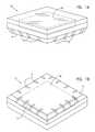
- FIGS. 1A and 1Bare pictorial illustrations of a crystalline substrate based device having an internal cavity, constructed and operative in accordance with a preferred embodiment of the present invention
- FIGS. 2A, 2B, 2 C & 2 Dare simplified sectional illustrations of various crystalline substrate based devices constructed and operative in accordance with a preferred embodiment of the present invention, corresponding generally to FIGS. 1A and 1B;
- FIG. 3is a partially cut-away sectional illustration of a crystalline substrate based device of the type shown in FIGS. 1A & 1B;
- FIGS. 4A, 4B, 4 C, 4 D & 4 Eare simplified illustrations of steps in a method for producing a packaging layer for use in crystalline substrate based device in accordance with a preferred embodiment of the present invention
- FIGS. 5A, 5B, 5 C, 5 D, 5 E, 5 F, 5 G, 5 H & 5 Iare simplified illustrations of steps in a method for producing a crystalline substrate based device of the type shown in FIGS. 2A & 2C in accordance with a preferred embodiment of the present invention
- FIGS. 6A, 6B, 6 C, 6 D, 6 E, 6 F, 6 G, 6 H, 61 , 6 J & 6 Kare simplified illustrations of steps in a method for producing a crystalline substrate based device of the type shown in FIG. 2B in accordance with another preferred embodiment of the present invention
- FIGS. 7A, 7B, 7 C, 7 D, 7 E, 7 F & 7 Gare simplified illustrations of steps in a method for producing a crystalline substrate based device of the type shown in FIG. 2D in accordance with another preferred embodiment of the present invention.
- FIGS. 8A and 8Bare illustrations of apparatus typically employed in the manufacture of a crystalline substrate based devices of the type shown in FIGS. 2A & 2C in the manner shown in FIGS. 5A - 5 I;
- FIGS. 9A and 9Bare illustrations of apparatus typically employed in the manufacture of a crystalline substrate based devices of the type shown in FIG. 2B in the manner shown in FIGS. 6A - 6 K;
- FIGS. 10A and 10Bare illustrations of apparatus typically employed in the manufacture of a crystalline substrate based devices of the type shown in FIG. 2D in the manner shown in FIGS. 7A - 7 G.
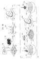
- FIGS. 1A and 1Billustrate a preferred embodiment of integrated circuit device constructed and operative in accordance with a preferred embodiment of the present invention.
- the integrated circuit deviceincludes a relatively thin and compact, environmentally protected and mechanically strengthened integrated circuit package 10 having a multiplicity of electrical contacts 12 plated along the edge surfaces 14 thereof.
- contacts 12extend over edge surfaces onto the planar surfaces 16 of the package.
- This contact arrangementpermits both flat surface mounting and edge mounting of package 10 onto a circuit board.
- the integrated circuit package 10may include one or more of the following elements (not shown): an integrally formed dichroic filter, color filter, antireflective coating, polarizer, optical grating, integrated wave guide and optical coupling bumps.
- the integrated circuit package 10defines a cavity 18 , which is indicated in phantom lines.
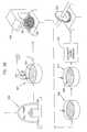
- FIGS. 2A - 2 Dillustrate four alternative preferred embodiments of integrated circuit devices of the general type shown in FIGS. 1A & 1B, constructed and operative in accordance with another preferred embodiment of the present invention.
- Each of the devices shown in FIGS. 2A - 2 Dincludes a relatively thin and compact, environmentally protected and mechanically strengthened integrated circuit package having a multiplicity of electrical contacts plated along the edge surfaces thereof.
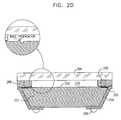
- FIG. 2Ashows an integrated circuit device including a microlens array 100 formed on a crystalline substrate 102 .
- a packaging layer 106typically formed of glass, along edges of which are formed electrical contacts 108 , typically defining bumps 110 .
- Conductive pads 112preferably connect substrate 102 to electrical contacts 108 .
- a packaging layer 114typically formed of glass, and associated spacer elements 116 , are sealed, by means of an adhesive such as epoxy 118 , over substrate 102 so as to define a cavity 120 between the microlens array 100 and layer 114 .
- packaging layer 114is preferably transparent and may have formed thereon a dichroic filter and/or anti-reflective coating.
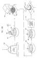
- FIG. 2Bshows an integrated circuit device including an optoelectronic or electromechanical device 150 , such as a chemical sensor, a micromirror array or an accelerometer is suspended on a crystalline substrate 152 , as by an electrically conductive connector 154 . Sealed onto substrate 152 is a packaging layer 156 typically formed of glass, along edges of which are formed electrical contacts 158 , typically defining bumps 160 . Conductive pads 162 preferably connect substrate 152 to electrical contacts 158 .
- an optoelectronic or electromechanical device 150such as a chemical sensor, a micromirror array or an accelerometer is suspended on a crystalline substrate 152 , as by an electrically conductive connector 154 .
- Sealed onto substrate 152is a packaging layer 156 typically formed of glass, along edges of which are formed electrical contacts 158 , typically defining bumps 160 .
- Conductive pads 162preferably connect substrate 152 to electrical contacts 158 .
- a packaging layer 164typically formed of glass, and associated spacer elements 166 , are sealed, by means of an adhesive, such as epoxy 168 , over substrate 152 so as to define first and second cavities 170 and 172 between the device 150 and both layer 164 and layer 156 .
- packaging layer 164is preferably transparent and may have formed thereon a dichroic filter and/or anti-reflective coating.
- FIG. 2Cshows an integrated circuit device including a optoelectronic or electromechanical device 200 formed on a crystalline substrate 202 .
- a packaging layer 206typically formed of glass, along edges of which are formed electrical contacts 208 , typically defining bumps 210 .
- Conductive pads 212preferably connect substrate 202 to electrical contacts 208 .
- a packaging layer 214typically formed of glass, and associated spacer elements 216 , are sealed, by means of an adhesive such as epoxy 218 , over substrate 202 so as to define a cavity 220 between the device 200 and layer 214 .
- packaging layer 214is preferably transparent and may have formed thereon a dichroic filter and/or anti-reflective coating.
- FIG. 2Dshows a Surface Acoustic Wave (SAW) device including a SAW propagation surface 250 defined on a crystalline substrate 252 , along edges of which are formed electrical contacts 258 , typically defining bumps 260 .
- Conductive pads 262preferably connect substrate 252 to electrical contacts 258 .
- a packaging layer 264typically formed of glass, and associated spacer elements 266 , are sealed, by means of an adhesive such as epoxy 268 , over substrate 252 so as to define a cavity 270 between surface 250 and layer 264 .
- FIG. 3is a partially cut away illustration of a typical integrated circuit device of the type shown in FIGS. 1A - 2 D, having a cavity as indicated by reference numeral 280 .
- FIGS. 4A, 4B, 4 C, 4 D & 4 Eare simplified illustrations of steps in a method for producing a packaging layer for use in crystalline substrate based device in accordance with a preferred embodiment of the present invention.
- a substrate 300typically formed of glass, is preferably coated with a layer 302 of epoxy based photoresist, typically SU-8 photoresist, commercially available from MicroChem Corp. of Newton, Mass., USA.
- the photoresist layer 302is exposed via a mask 304 , as shown in FIG. 4C and washed to define spacers 306 shown in FIG. 4D, which are typically of rectangular configuration, as indicated in FIG. 4E. These spacers correspond to spacer elements 116 , 166 , 216 and 266 in FIGS. 2A - 2 D respectively.
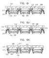
- FIGS. 5A, 5B, 5 C, 5 D, 5 E, 5 F, 5 G, 5 H & 5 Iare simplified illustrations of steps in a method for producing a crystalline substrate based device of the type shown in FIGS. 2A & 2C in accordance with a preferred embodiment of the present invention.
- a packaging layer 400typically of the type shown in FIGS. 4D and 4E is provided.
- Adhesive 402is applied thereto, preferably adjacent and between spacers 406 formed thereon, which correspond to the spacers 306 shown in FIGS. 4D & 4E respectively and also correspond to spacer elements 116 , 166 , 216 and 266 in FIGS. 2A - 2 D respectively.
- Adhesive 402is preferably a high temperature epoxy, such as EPO-TEK 353ND, commercially available from Epoxy Technology Inc. of Billerica, Mass., USA.
- the packaging layer 400As shown in FIG. 5B, the packaging layer 400 , thus prepared, is adhered to a crystalline substrate 404 , typically having at least one metal layer thereon and having mounted thereon optomechanical or optoelectronic devices of the types described hereinabove with reference to FIGS. 2A & 2C. As seen clearly, a cavity 405 is defined between the packaging layer 400 and the substrate 404 , in accordance with a preferred embodiment of the present invention.
- the crystalline substrate 404is preferably lapped, as shown in FIG. 5C and etched, as shown in FIG. 5D, to define separate substrates 407 . Following etching, the substrates 407 are adhered via an epoxy layer 408 to an underlying packaging layer 410 , as shown in FIG. 5E.
- the packaging layer 410 and epoxy layer 408are mechanically notched and thereafter electrical contacts 412 and typically bumps 414 are formed thereon, as seen in FIG. 5G.
- the resulting assemblyis diced as shown in FIG. 5H to yield a plurality of packaged integrated circuit devices, as seen in FIG. 5I.
- the crystalline substratemay be any suitable crystalline substrate and may comprise, for example, silicon, lithium niobate, lithium tantalate or quartz.
- FIGS. 6A, 6B, 6 C, 6 D, 6 E, 6 F, 6 G, 6 H, 61 , 6 J & 6 Kare simplified illustrations of steps in a method for producing a crystalline substrate based device of the type shown in FIG. 2B in accordance with another preferred embodiment of the present invention.
- a substrate 500mounted on a substrate 500 , typically formed of Pyrex are a plurality of crystalline substrates 502 onto which are formed pads 504 and onto which are suspended, as by electrically conductive connectors 506 , optoelectronic or electromechanical devices 508 , such as chemical sensors, micromirror arrays or an accelerometer, which may correspond to devices 150 of the type shown in FIG. 2B.
- a substrate 500typically formed of Pyrex are a plurality of crystalline substrates 502 onto which are formed pads 504 and onto which are suspended, as by electrically conductive connectors 506 , optoelectronic or electromechanical devices 508 , such as chemical sensors, micromirror arrays or an accelerometer, which may correspond to devices 150 of the type shown in FIG. 2B.
- a packaging layer 510typically of the type shown in FIGS. 4D and 4E, is provided having adhesive 512 applied thereto, preferably adjacent and between spacers 516 formed thereon, which correspond to the spacers 306 shown in FIGS. 4D & 4E respectively and also correspond to spacer elements 116 , 166 , 216 and 266 in FIGS. 2A - 2 D respectively.
- Adhesive 512is preferably a high temperature epoxy, such as EPO-TEK 353ND, commercially available from Epoxy Technology Inc. of Billerica, Mass., USA.
- the packaging layer 510As seen in FIG. 6C, the packaging layer 510 , thus prepared, is adhered to crystalline substrates 502 , typically adjacent pads 504 . As seen clearly, a cavity 513 is defined between the packaging layer 510 and the substrates 502 , and another cavity 514 is defined between substrates 502 , substrate 500 and electromechanical devices 508 in accordance with a preferred embodiment of the present invention.
- the substrate 500 and crystalline substrates 502are preferably notched, as shown in FIG. 6D and etched, as shown in FIG. 6E, to define volumes 515 in crystalline substrates 502 which are preferably filled with epoxy 517 , as shown in FIG. 6F.
- the substrate 500 , the epoxy 516 and the adhesive 512are then mechanically notched to form a notch 501 , and thereafter electrical contacts 519 are formed thereon, as by sputtering, as shown in FIG. 6H.
- Bumps 518are formed thereon, as seen in FIG. 61, preferably together with a NiAu coating.
- the resulting assemblyis diced as shown in FIG. 6J to yield a plurality of packaged integrated circuit devices, as seen in FIG. 6K.
- FIGS. 7A, 7B, 7 C, 7 D, 7 E, 7 F & 7 Gare simplified illustrations of steps in a method for producing a crystalline substrate based device of the type shown in FIG. 2D in accordance with another preferred embodiment of the present invention.
- a packaging layer 600typically of the type shown in Figs. 4D and 4E is provided.
- Adhesive 602is applied thereto, preferably adjacent and between spacers 606 formed thereon, which correspond to the spacers 306 shown in FIGS. 4D & 4E respectively and also correspond to spacer elements 116 , 166 , 216 and 266 in FIGS. 2A - 2 D respectively.
- Adhesive 602is preferably a high temperature epoxy, such as EPO-TEK 353ND, commercially available from Epoxy Technology Inc. of Billerica, Mass., USA.
- the packaging layer 600As shown in FIG. 7B, the packaging layer 600 , thus prepared, is adhered to a crystalline substrate 604 , typically having at least one metal layer thereon and having defined thereon a SAW propagation layer 609 as described hereinabove with reference to FIG. 2D. As seen clearly, a cavity 607 is defined between the packaging layer 600 and the SAW propagation layer 609 , in accordance with a preferred embodiment of the present invention.
- the crystalline substrate 604can be lapped, as shown in FIG. 7C and notched partially into the adhesive 602 , as shown in FIG. 7D, to define separate substrates 608 .
- electrical contacts 610 and typically bumps 614are formed thereon, as seen in FIG. 7E.
- the resulting assemblyis diced as shown in FIG. 7F to yield a plurality of packaged SAW devices, as seen in FIG. 7G.
- FIGS. 8A and 8Bare illustrations of apparatus employed in the manufacture of a crystalline substrate based devices of the type shown in FIGS. 2A & 2C in the manner shown in FIGS. 5A - 5 I.
- a conventional wafer fabrication facility 680provides complete wafers 681 , of the type shown in FIG. 5A.
- Individual wafers 682are bonded on their active surfaces to protective layers 683 as shown in FIGS. 5A & 5B, by bonding apparatus 685 , preferably having facilities for rotation of the wafer 682 , the layer 683 and the epoxy so as to obtain even distribution of the epoxy.
- the bonded wafer 686is thinned (FIG. 5C) at its non-active surface as by grinding apparatus 684 , such as Model 32B TGW using 12.5 A abrasive 687 , which is commercially available from Speedfam Machines Co. Ltd. of England.
- the waferis then etched (FIG. 5D) at its non-active surface, preferably by photolithography, such as by using conventional spin-coated photoresist, which is commercially available from Hoechst, under the brand designation AZ 4562, using a mask exposure machine 692 for the exposure of light sensitive photoresist 690 through the mask 691 and later etching the silicon in a bath 693 using solution 699 .
- photolithographysuch as by using conventional spin-coated photoresist, which is commercially available from Hoechst, under the brand designation AZ 4562
- the etched wafer 1000is bonded (FIG. 5E) on the non-active side to protective layer 686 by bonding apparatus 694 , which may be essentially the same as apparatus 685 , to produce a doubly bonded wafer sandwich.
- Notching apparatus 695partially cuts the bonded wafer sandwich of FIG. 5E to the configuration shown in FIG. 5F.
- the notched wafer 1002is then preferably subjected to anti-corrosion treatment in a bath 696 , containing a chromating solution 698 , such as described in any of the following U.S. Pat. Nos.: 2,507,956; 2,851,385 and 2,796,370, the disclosure of which is hereby incorporated by reference.
- Conductive layer deposition apparatus 700which operates by vacuum deposition techniques, such as a Model 903M sputtering machine manufactured by Material Research Corporation of the U.S.A., is employed to produce a conductive layer on one or more surfaces of each die of the wafer as shown in FIG. 5G.
- vacuum deposition techniquessuch as a Model 903M sputtering machine manufactured by Material Research Corporation of the U.S.A.
- Configuration of contact stripsis carried out preferably by using conventional electro-deposited photoresist 701 , which is commercially available from DuPont under the brand name Primecoat or from Shipley, under the brand name Eagle.
- the photoresist 701is applied to the wafers 707 in a photoresist bath assembly 702 , which is commercially available from DuPont or Shipley.
- the photoresist 703is preferably light configured by a UV exposure system 704 , which may be identical to system 692 , using a mask 705 to define suitable etching patterns.
- the photoresistis then developed in a development bath 706 , and then the wafer is etched in a metal etch solution 708 located in an etching bath 710 , thus providing a conductor configuration such as that shown in FIG. 5G.
- the exposed conductive strips shown in FIG. 5Gare then plated, preferably by electroless plating apparatus 712 , which is commercially available from Okuno of Japan.
- the waferis then diced (FIG. 5H) into individual pre-packaged integrated circuit devices.
- the dicing blade 714should be a diamond resinoid blade of thickness 4 - 12 mils.
- the resulting diesappear as illustrated generally in FIG. 51.
- FIGS. 9A and 9Bare illustrations apparatus employed in the manufacture of a crystalline substrate based devices of the type shown in FIG. 2B in the manner shown in FIGS. 6A - 6 K.
- a wafer fabrication facility 780provides complete wafers 781 , of the type shown in FIG. 6A mounted onto a substrate, such as a Pyrex substrate 782 .
- Individual wafers 781are bonded on their active surfaces to protective layers 783 as shown in FIGS. 6B & 6C, by bonding apparatus 784 , preferably having facilities for rotation of the wafer 781 , the layer 783 and the epoxy so as to obtain even distribution of the epoxy.
- Notching apparatus 794partially cuts the bonded wafer sandwich 793 of FIG. 6C to the configuration shown in FIG. 6D.
- the notched wafer 796is then etched in a silicon etching solution 798 in a bath 1010 .
- the etched voids 1012 in wafer 1014are filled with epoxy 1016 , using a dispenser 1018 to fill the voids 1012 , to obtain epoxy filled voids 1020 .
- the wafer 1022is notched again using apparatus 1024 through the epoxy filled trenches 1020 .
- the notched wafer 1028is then preferably subjected to anti-corrosion treatment in a bath 1030 , containing a chromating solution 1032 , such as described in any of the following U.S. Pat. Nos.: 2,507,956; 2,851,385 and 2,796,370, the disclosure of which is hereby incorporated by reference.
- Conductive layer deposition apparatus 800which operates by vacuum deposition techniques, such as a Model 903M sputtering machine manufactured by Material Research Corporation of the U.S.A., is employed to produce a conductive layer on one or more surfaces of each die of the wafer as shown in FIG. 6G.
- Configuration of contact stripsis carried out preferably by using conventional electro-deposited photoresist 801 , which is commercially available from DuPont under the brand name Primecoat or from Shipley, under the brand name Eagle.
- the photoresistis applied to the wafers 803 in a photoresist bath assembly 802 , which is commercially available from DuPont or Shipley.
- the photoresist 807is preferably light configured by a UV exposure system 804 using a mask 805 to define suitable etching patterns.
- the photoresistis then developed in a development bath 806 , and then etched in a metal etch solution 808 located in an etching bath 810 , thus providing a conductor configuration such as that shown in FIG. 1B.
- the exposed conductive strips shown in FIG. 6Gare then plated, preferably by electroless plating apparatus 812 , which is commercially available from Okuno of Japan.
- the waferis then diced (FIG. 6H) into individual pre-packaged integrated circuit devices.
- the dicing blade 814should be a diamond resinoid blade of thickness 4 - 12 mils.
- the resulting diesappear as illustrated generally in FIG. 6K.
- FIGS. 1 OA and lOBare illustrations apparatus employed in the manufacture of a crystal line substrate based device of the type shown in FIG. 2D in the manner shown in FIGS. 7A - 7 G.
- a conventional wafer fabrication facility 880provides complete wafers 881 , of the type shown in FIG. 7A. Individual wafers 881 are bonded on their active surfaces to protective layers 883 as shown in FIGS. 7A & 7B, by bonding apparatus 882 , preferably having facilities for rotation of the wafer 881 , the layer 883 and the epoxy so as to obtain even distribution of the epoxy.
- Notching apparatus 894partially cuts the wafer 883 of FIG. 7E to the configuration shown in FIG. 7F.
- the notched wafer 884is then preferably subjected to anti-corrosion treatment in a bath 896 , containing a chromating solution 898 , such as described in any of the following U.S. Pat. Nos.: 2,507,956; 2,851,385 and 2,796,370, the disclosure of which is hereby incorporated by reference.
- Conductive layer deposition apparatus 900which operates by vacuum deposition techniques, such as a Model 903M sputtering machine manufactured by Material Research Corporation of the U.S.A., is employed to produce a conductive layer on one or more surfaces of each die of the wafer as shown in FIG. 7G.
- Configuration of contact stripsis carried out preferably by using conventional electro-deposited photoresist 901 , which is commercially available from DuPont under the brand name Primecoat or from Shipley, under the brand name Eagle.
- the photoresist 901is applied to the wafers 903 in a photoresist bath assembly 902 , which is commercially available from DuPont or Shipley.
- the photoresist 920is preferably light configured by a UV exposure system 904 using a mask 905 to define suitable etching patterns.
- the photoresistis then developed in a development bath 906 , and then etched in a metal etch solution 908 located in an etching bath 910 , thus providing a conductor configuration such as that shown in FIG. 1B.
- the exposed conductive strips shown in FIG. 7Gare then plated, preferably by electroless plating apparatus 912 , which is commercially available from Okuno of Japan.
- the wafer 913is then diced (FIG. 5H) into individual pre-packaged integrated circuit devices.
- the dicing blade 914should be a diamond resinoid blade of thickness 4 - 12 mils.
- the resulting diesappear as illustrated generally in FIG. 7G.
Landscapes
- Engineering & Computer Science (AREA)
- Microelectronics & Electronic Packaging (AREA)
- Computer Hardware Design (AREA)
- Physics & Mathematics (AREA)
- Acoustics & Sound (AREA)
- Manufacturing & Machinery (AREA)
- Condensed Matter Physics & Semiconductors (AREA)
- General Physics & Mathematics (AREA)
- Power Engineering (AREA)
- Micromachines (AREA)
- Surface Acoustic Wave Elements And Circuit Networks Thereof (AREA)
Abstract
Description
- The present invention relates to integrated circuits and similar devices generally and to methods for the manufacture thereof.[0001]
- An essential step in the manufacture of all integrated circuit devices is known as “packaging” and involves mechanical and environmental protection of a silicon chip which is at the heart of the integrated circuit as well as electrical interconnection between predetermined locations on the silicon chip and external electrical terminals.[0002]
- At present three principal technologies are employed for packaging semiconductors: wire bonding, tape automatic bonding (TAB) and flip chip.[0003]
- Wire bonding employs heat and ultrasonic energy to weld gold bonding wires between bond pads on the chip and contacts on the package.[0004]
- Tape automatic bonding (TAB) employs a copper foil tape instead of bonding wire. The copper foil tape is configured for each specific die and package combination and includes a pattern of copper traces suited thereto. The individual leads may be connected individually or as a group to the various bond pads on the chip.[0005]
- Flip chips are integrated circuit dies which have solder bumps formed on top of the bonding pads, thus allowing the die to be “flipped” circuit side down and directly soldered to a substrate. Wire bonds are not required and considerable savings in package spacing may be realized.[0006]
- The above-described technologies each have certain limitations. Both wire bonding and TAB bonding are prone to bad bond formation and subject the die to relatively high temperatures and mechanical pressures. Both wire bond and TAB technologies are problematic from a package size viewpoint, producing integrated circuit devices having a die-to-package area ratio ranging from about 10% to 60%.[0007]
- The flip-chip does not provide packaging but rather only interconnection. The interconnection encounters problems of uniformity in the solder bumps as well as in thermal expansion mismatching, which limits the use of available substrates to silicon or materials which have thermal expansion characteristics similar to those of silicon.[0008]
- The patent literature is extremely rich in the area of integrated circuits and methods for the manufacture thereof.[0009]
- Described in applicant's published PCT Application WO 95/19645 are methods and apparatus for producing integrated circuit devices.[0010]
- The following U.S. Pat. Nos. and patent applications of the present inventor are considered to be particularly relevant: 5,716,759; 5,547,906; 5,455,455 and 08/952,019.[0011]
- The present invention seeks to provide improved packaged crystalline substrate based devices and methods for producing same.[0012]
- There is thus provided in accordance with a preferred embodiment of the present invention a crystalline substrate based device including a crystalline substrate having formed thereon a microstructure and at least one packaging layer which is sealed over the microstructure by an adhesive and defines therewith at least one gap between the crystalline substrate and the at least one packaging layer.[0013]
- There is also provided in accordance with a preferred embodiment of the present invention a chip scale packaged crystalline substrate including:[0014]
- a substrate having formed thereon a microstructure; and[0015]
- at least one chip scale package which is sealed over the microstructure and defines therewith at least one gap.[0016]
- There is additionally provided in accordance with a preferred embodiment of the present invention a method of producing a crystalline substrate based device including:[0017]
- providing a microstructure on a substrate; and[0018]
- adhesively sealing at least one packaging layer over the microstructure and at least partially spaced therefrom, thereby to define a gap between the microstructure and the at least one packaging layer.[0019]
- Preferably, at least one packaging layer is sealed onto the crystalline substrate using an adhesive, such as epoxy.[0020]
- In accordance with a preferred embodiment of the present invention, the crystalline substrate includes silicon, lithium niobate, lithium tantalate or quartz.[0021]
- Preferably, the at least one packaging layer is transparent.[0022]
- The at least one cavity may include a single cavity or a plurality of cavities.[0023]
- The microstructure may include a micromechanical structure, a microelectronic structure and/or an optoelectronic structure.[0024]
- FIGS. 1A and 1B are pictorial illustrations of a crystalline substrate based device having an internal cavity, constructed and operative in accordance with a preferred embodiment of the present invention;[0025]
- FIGS. 2A, 2B,[0026]2C &2D are simplified sectional illustrations of various crystalline substrate based devices constructed and operative in accordance with a preferred embodiment of the present invention, corresponding generally to FIGS. 1A and 1B;
- FIG. 3 is a partially cut-away sectional illustration of a crystalline substrate based device of the type shown in FIGS. 1A & 1B;[0027]
- FIGS. 4A, 4B,[0028]4C,4D &4E are simplified illustrations of steps in a method for producing a packaging layer for use in crystalline substrate based device in accordance with a preferred embodiment of the present invention;
- FIGS. 5A, 5B,[0029]5C,5D,5E,5F,5G,5H &5I are simplified illustrations of steps in a method for producing a crystalline substrate based device of the type shown in FIGS. 2A & 2C in accordance with a preferred embodiment of the present invention;
- FIGS. 6A, 6B,[0030]6C,6D,6E,6F,6G,6H,61,6J &6K are simplified illustrations of steps in a method for producing a crystalline substrate based device of the type shown in FIG. 2B in accordance with another preferred embodiment of the present invention;
- FIGS. 7A, 7B,[0031]7C,7D,7E,7F &7G are simplified illustrations of steps in a method for producing a crystalline substrate based device of the type shown in FIG. 2D in accordance with another preferred embodiment of the present invention;
- FIGS. 8A and 8B are illustrations of apparatus typically employed in the manufacture of a crystalline substrate based devices of the type shown in FIGS. 2A & 2C in the manner shown in FIGS. 5A -[0032]5I;
- FIGS. 9A and 9B are illustrations of apparatus typically employed in the manufacture of a crystalline substrate based devices of the type shown in FIG. 2B in the manner shown in FIGS. 6A -[0033]6K; and
- FIGS. 10A and 10B are illustrations of apparatus typically employed in the manufacture of a crystalline substrate based devices of the type shown in FIG. 2D in the manner shown in FIGS. 7A -[0034]7G.
- Reference is now made to FIGS. 1A and 1B, which together illustrate a preferred embodiment of integrated circuit device constructed and operative in accordance with a preferred embodiment of the present invention. The integrated circuit device includes a relatively thin and compact, environmentally protected and mechanically strengthened integrated[0035]
circuit package 10 having a multiplicity ofelectrical contacts 12 plated along the edge surfaces14 thereof. - Preferably,[0036]
contacts 12 extend over edge surfaces onto theplanar surfaces 16 of the package. This contact arrangement permits both flat surface mounting and edge mounting ofpackage 10 onto a circuit board. It is noted that theintegrated circuit package 10 may include one or more of the following elements (not shown): an integrally formed dichroic filter, color filter, antireflective coating, polarizer, optical grating, integrated wave guide and optical coupling bumps. - In accordance with a preferred embodiment of the present invention, the[0037]
integrated circuit package 10 defines acavity 18, which is indicated in phantom lines. - Reference is now made to FIGS. 2A -[0038]2D, which illustrate four alternative preferred embodiments of integrated circuit devices of the general type shown in FIGS. 1A & 1B, constructed and operative in accordance with another preferred embodiment of the present invention. Each of the devices shown in FIGS. 2A -2D includes a relatively thin and compact, environmentally protected and mechanically strengthened integrated circuit package having a multiplicity of electrical contacts plated along the edge surfaces thereof.
- FIG. 2A shows an integrated circuit device including a[0039]
microlens array 100 formed on acrystalline substrate 102. Underlying thesubstrate 102 and sealed thereto byepoxy 104 is apackaging layer 106, typically formed of glass, along edges of which are formedelectrical contacts 108, typically definingbumps 110.Conductive pads 112 preferably connectsubstrate 102 toelectrical contacts 108. - In accordance with a preferred embodiment of the present invention a[0040]
packaging layer 114, typically formed of glass, and associatedspacer elements 116, are sealed, by means of an adhesive such asepoxy 118, oversubstrate 102 so as to define acavity 120 between themicrolens array 100 andlayer 114. - It is appreciated that[0041]
packaging layer 114 is preferably transparent and may have formed thereon a dichroic filter and/or anti-reflective coating. - FIG. 2B shows an integrated circuit device including an optoelectronic or[0042]
electromechanical device 150, such as a chemical sensor, a micromirror array or an accelerometer is suspended on acrystalline substrate 152, as by an electricallyconductive connector 154. Sealed ontosubstrate 152 is apackaging layer 156 typically formed of glass, along edges of which are formedelectrical contacts 158, typically definingbumps 160.Conductive pads 162 preferably connectsubstrate 152 toelectrical contacts 158. - In accordance with a preferred embodiment of the present invention a[0043]
packaging layer 164, typically formed of glass, and associatedspacer elements 166, are sealed, by means of an adhesive, such asepoxy 168, oversubstrate 152 so as to define first andsecond cavities device 150 and bothlayer 164 andlayer 156. - It is appreciated that[0044]
packaging layer 164 is preferably transparent and may have formed thereon a dichroic filter and/or anti-reflective coating. - FIG. 2C shows an integrated circuit device including a optoelectronic or[0045]
electromechanical device 200 formed on acrystalline substrate 202. Underlying thesubstrate 202 and sealed thereto byepoxy 204 is apackaging layer 206, typically formed of glass, along edges of which are formedelectrical contacts 208, typically definingbumps 210.Conductive pads 212 preferably connectsubstrate 202 toelectrical contacts 208. - In accordance with a preferred embodiment of the present invention a[0046]
packaging layer 214, typically formed of glass, and associatedspacer elements 216, are sealed, by means of an adhesive such asepoxy 218, oversubstrate 202 so as to define acavity 220 between thedevice 200 andlayer 214. - It is appreciated that[0047]
packaging layer 214 is preferably transparent and may have formed thereon a dichroic filter and/or anti-reflective coating. - FIG. 2D shows a Surface Acoustic Wave (SAW) device including a[0048]
SAW propagation surface 250 defined on acrystalline substrate 252, along edges of which are formedelectrical contacts 258, typically definingbumps 260.Conductive pads 262 preferably connectsubstrate 252 toelectrical contacts 258. - In accordance with a preferred embodiment of the present invention a[0049]
packaging layer 264, typically formed of glass, and associatedspacer elements 266, are sealed, by means of an adhesive such asepoxy 268, oversubstrate 252 so as to define acavity 270 betweensurface 250 andlayer 264. - Reference is now made to FIG. 3, which is a partially cut away illustration of a typical integrated circuit device of the type shown in FIGS. 1A -[0050]2D, having a cavity as indicated by
reference numeral 280. - Reference is now made to FIGS. 4A, 4B,[0051]4C,4D &4E, which are simplified illustrations of steps in a method for producing a packaging layer for use in crystalline substrate based device in accordance with a preferred embodiment of the present invention. As seen in FIGS. 4A & 4B, a
substrate 300, typically formed of glass, is preferably coated with alayer 302 of epoxy based photoresist, typically SU-8 photoresist, commercially available from MicroChem Corp. of Newton, Mass., USA. - The[0052]
photoresist layer 302 is exposed via amask 304, as shown in FIG. 4C and washed to definespacers 306 shown in FIG. 4D, which are typically of rectangular configuration, as indicated in FIG. 4E. These spacers correspond to spacerelements - Reference is now made to FIGS. 5A, 5B,[0053]5C,5D,5E,5F,5G,5H &5I, which are simplified illustrations of steps in a method for producing a crystalline substrate based device of the type shown in FIGS. 2A & 2C in accordance with a preferred embodiment of the present invention.
- As seen in FIG. 5A, a[0054]
packaging layer 400, typically of the type shown in FIGS. 4D and 4E is provided.Adhesive 402 is applied thereto, preferably adjacent and betweenspacers 406 formed thereon, which correspond to thespacers 306 shown in FIGS. 4D & 4E respectively and also correspond to spacerelements Adhesive 402 is preferably a high temperature epoxy, such as EPO-TEK 353ND, commercially available from Epoxy Technology Inc. of Billerica, Mass., USA. - As shown in FIG. 5B, the[0055]
packaging layer 400, thus prepared, is adhered to acrystalline substrate 404, typically having at least one metal layer thereon and having mounted thereon optomechanical or optoelectronic devices of the types described hereinabove with reference to FIGS. 2A & 2C. As seen clearly, acavity 405 is defined between thepackaging layer 400 and thesubstrate 404, in accordance with a preferred embodiment of the present invention. - The[0056]
crystalline substrate 404 is preferably lapped, as shown in FIG. 5C and etched, as shown in FIG. 5D, to defineseparate substrates 407. Following etching, thesubstrates 407 are adhered via anepoxy layer 408 to anunderlying packaging layer 410, as shown in FIG. 5E. - As seen in FIG. 5F, the[0057]
packaging layer 410 andepoxy layer 408 are mechanically notched and thereafterelectrical contacts 412 and typically bumps414 are formed thereon, as seen in FIG. 5G. The resulting assembly is diced as shown in FIG. 5H to yield a plurality of packaged integrated circuit devices, as seen in FIG. 5I. - It is appreciated that here and throughout all of the examples described herein, the crystalline substrate may be any suitable crystalline substrate and may comprise, for example, silicon, lithium niobate, lithium tantalate or quartz.[0058]
- The manufacturing techniques described hereinabove and hereinbelow may but need not necessarily include techniques described in any of the following U.S. Pat. Nos. and patent applications of the present inventor/assignee, the disclosure of which is hereby incorporated by reference: 5,716,759; 5,547,906; 5,455,455 and 08/952,019.[0059]
- Reference is now made to FIGS. 6A, 6B,[0060]6C,6D,6E,6F,6G,6H,61,6J &6K, which are simplified illustrations of steps in a method for producing a crystalline substrate based device of the type shown in FIG. 2B in accordance with another preferred embodiment of the present invention.
- As seen in FIG. 6A, mounted on a[0061]
substrate 500, typically formed of Pyrex are a plurality ofcrystalline substrates 502 onto which are formedpads 504 and onto which are suspended, as by electricallyconductive connectors 506, optoelectronic orelectromechanical devices 508, such as chemical sensors, micromirror arrays or an accelerometer, which may correspond todevices 150 of the type shown in FIG. 2B. - As shown in FIG. 6B, a[0062]
packaging layer 510, typically of the type shown in FIGS. 4D and 4E, is provided having adhesive512 applied thereto, preferably adjacent and betweenspacers 516 formed thereon, which correspond to thespacers 306 shown in FIGS. 4D & 4E respectively and also correspond to spacerelements Adhesive 512 is preferably a high temperature epoxy, such as EPO-TEK 353ND, commercially available from Epoxy Technology Inc. of Billerica, Mass., USA. - As seen in FIG. 6C, the[0063]
packaging layer 510, thus prepared, is adhered tocrystalline substrates 502, typicallyadjacent pads 504. As seen clearly, acavity 513 is defined between thepackaging layer 510 and thesubstrates 502, and anothercavity 514 is defined betweensubstrates 502,substrate 500 andelectromechanical devices 508 in accordance with a preferred embodiment of the present invention. - The[0064]
substrate 500 andcrystalline substrates 502 are preferably notched, as shown in FIG. 6D and etched, as shown in FIG. 6E, to definevolumes 515 incrystalline substrates 502 which are preferably filled withepoxy 517, as shown in FIG. 6F. - As seen in FIG. 6G, the[0065]
substrate 500, the epoxy516 and the adhesive512 are then mechanically notched to form anotch 501, and thereafterelectrical contacts 519 are formed thereon, as by sputtering, as shown in FIG. 6H.Bumps 518 are formed thereon, as seen in FIG. 61, preferably together with a NiAu coating. The resulting assembly is diced as shown in FIG. 6J to yield a plurality of packaged integrated circuit devices, as seen in FIG. 6K. - Reference is now made to FIGS. 7A, 7B,[0066]7C,7D,7E,7F &7G, which are simplified illustrations of steps in a method for producing a crystalline substrate based device of the type shown in FIG. 2D in accordance with another preferred embodiment of the present invention.
- As seen in FIG. 7A, a[0067]
packaging layer 600, typically of the type shown in Figs. 4D and 4E is provided.Adhesive 602 is applied thereto, preferably adjacent and betweenspacers 606 formed thereon, which correspond to thespacers 306 shown in FIGS. 4D & 4E respectively and also correspond to spacerelements Adhesive 602 is preferably a high temperature epoxy, such as EPO-TEK 353ND, commercially available from Epoxy Technology Inc. of Billerica, Mass., USA. - As shown in FIG. 7B, the[0068]
packaging layer 600, thus prepared, is adhered to acrystalline substrate 604, typically having at least one metal layer thereon and having defined thereon aSAW propagation layer 609 as described hereinabove with reference to FIG. 2D. As seen clearly, acavity 607 is defined between thepackaging layer 600 and theSAW propagation layer 609, in accordance with a preferred embodiment of the present invention. - The[0069]
crystalline substrate 604 can be lapped, as shown in FIG. 7C and notched partially into the adhesive602, as shown in FIG. 7D, to defineseparate substrates 608. Following etching,electrical contacts 610 and typically bumps614 are formed thereon, as seen in FIG. 7E. The resulting assembly is diced as shown in FIG. 7F to yield a plurality of packaged SAW devices, as seen in FIG. 7G. - Reference is now made to FIGS. 8A and 8B, which are illustrations of apparatus employed in the manufacture of a crystalline substrate based devices of the type shown in FIGS. 2A & 2C in the manner shown in FIGS. 5A -[0070]5I. As seen in FIGS. 8A and 8B, a conventional
wafer fabrication facility 680 providescomplete wafers 681, of the type shown in FIG. 5A. Individual wafers682 are bonded on their active surfaces toprotective layers 683 as shown in FIGS. 5A & 5B, by bondingapparatus 685, preferably having facilities for rotation of the wafer682, thelayer 683 and the epoxy so as to obtain even distribution of the epoxy. - The bonded[0071]
wafer 686 is thinned (FIG. 5C) at its non-active surface as by grindingapparatus 684, such as Model 32B TGW using 12.5 A abrasive687, which is commercially available from Speedfam Machines Co. Ltd. of England. - The wafer is then etched (FIG. 5D) at its non-active surface, preferably by photolithography, such as by using conventional spin-coated photoresist, which is commercially available from Hoechst, under the brand designation AZ 4562, using a[0072]
mask exposure machine 692 for the exposure of lightsensitive photoresist 690 through themask 691 and later etching the silicon in abath 693 usingsolution 699. - The etched[0073]
wafer 1000 is bonded (FIG. 5E) on the non-active side toprotective layer 686 bybonding apparatus 694, which may be essentially the same asapparatus 685, to produce a doubly bonded wafer sandwich. - Notching[0074]
apparatus 695 partially cuts the bonded wafer sandwich of FIG. 5E to the configuration shown in FIG. 5F. - The notched[0075]
wafer 1002 is then preferably subjected to anti-corrosion treatment in abath 696, containing achromating solution 698, such as described in any of the following U.S. Pat. Nos.: 2,507,956; 2,851,385 and 2,796,370, the disclosure of which is hereby incorporated by reference. - Conductive[0076]
layer deposition apparatus 700, which operates by vacuum deposition techniques, such as a Model 903M sputtering machine manufactured by Material Research Corporation of the U.S.A., is employed to produce a conductive layer on one or more surfaces of each die of the wafer as shown in FIG. 5G. - Configuration of contact strips, as shown in FIG. 5G, is carried out preferably by using conventional electro-deposited photoresist[0077]701, which is commercially available from DuPont under the brand name Primecoat or from Shipley, under the brand name Eagle. The photoresist701 is applied to the
wafers 707 in aphotoresist bath assembly 702, which is commercially available from DuPont or Shipley. - The[0078]
photoresist 703 is preferably light configured by aUV exposure system 704, which may be identical tosystem 692, using amask 705 to define suitable etching patterns. The photoresist is then developed in adevelopment bath 706, and then the wafer is etched in ametal etch solution 708 located in anetching bath 710, thus providing a conductor configuration such as that shown in FIG. 5G. - The exposed conductive strips shown in FIG. 5G are then plated, preferably by[0079]
electroless plating apparatus 712, which is commercially available from Okuno of Japan. - The wafer is then diced (FIG. 5H) into individual pre-packaged integrated circuit devices. Preferably the[0080]
dicing blade 714 should be a diamond resinoid blade of thickness 4 - 12 mils. The resulting dies appear as illustrated generally in FIG. 51. - Reference is now made to FIGS. 9A and 9B, which are illustrations apparatus employed in the manufacture of a crystalline substrate based devices of the type shown in FIG. 2B in the manner shown in FIGS. 6A -[0081]6K. As seen in FIGS. 9A and 9B, a
wafer fabrication facility 780 providescomplete wafers 781, of the type shown in FIG. 6A mounted onto a substrate, such as aPyrex substrate 782.Individual wafers 781 are bonded on their active surfaces toprotective layers 783 as shown in FIGS. 6B & 6C, by bondingapparatus 784, preferably having facilities for rotation of thewafer 781, thelayer 783 and the epoxy so as to obtain even distribution of the epoxy. - Notching[0082]
apparatus 794 partially cuts the bondedwafer sandwich 793 of FIG. 6C to the configuration shown in FIG. 6D. The notchedwafer 796 is then etched in asilicon etching solution 798 in abath 1010. The etchedvoids 1012 inwafer 1014 are filled with epoxy1016, using adispenser 1018 to fill thevoids 1012, to obtain epoxy filled voids1020. Thewafer 1022 is notched again usingapparatus 1024 through the epoxy filledtrenches 1020. - The notched[0083]
wafer 1028 is then preferably subjected to anti-corrosion treatment in abath 1030, containing achromating solution 1032, such as described in any of the following U.S. Pat. Nos.: 2,507,956; 2,851,385 and 2,796,370, the disclosure of which is hereby incorporated by reference. - Conductive[0084]
layer deposition apparatus 800, which operates by vacuum deposition techniques, such as a Model 903M sputtering machine manufactured by Material Research Corporation of the U.S.A., is employed to produce a conductive layer on one or more surfaces of each die of the wafer as shown in FIG. 6G. - Configuration of contact strips, as shown in FIG. 6E, is carried out preferably by using conventional electro-deposited[0085]
photoresist 801, which is commercially available from DuPont under the brand name Primecoat or from Shipley, under the brand name Eagle. The photoresist is applied to thewafers 803 in aphotoresist bath assembly 802, which is commercially available from DuPont or Shipley. - The[0086]
photoresist 807 is preferably light configured by aUV exposure system 804 using amask 805 to define suitable etching patterns. The photoresist is then developed in adevelopment bath 806, and then etched in ametal etch solution 808 located in anetching bath 810, thus providing a conductor configuration such as that shown in FIG. 1B. - The exposed conductive strips shown in FIG. 6G are then plated, preferably by[0087]
electroless plating apparatus 812, which is commercially available from Okuno of Japan. - The wafer is then diced (FIG. 6H) into individual pre-packaged integrated circuit devices. Preferably the[0088]
dicing blade 814 should be a diamond resinoid blade of thickness 4 - 12 mils. The resulting dies appear as illustrated generally in FIG. 6K. - Reference is now made to FIGS.[0089]1OA and lOB, which are illustrations apparatus employed in the manufacture of a crystal line substrate based device of the type shown in FIG. 2D in the manner shown in FIGS. 7A -7G. As seen in FIGS. 10A and 10B, a conventional
wafer fabrication facility 880 providescomplete wafers 881, of the type shown in FIG. 7A.Individual wafers 881 are bonded on their active surfaces toprotective layers 883 as shown in FIGS. 7A & 7B, by bondingapparatus 882, preferably having facilities for rotation of thewafer 881, thelayer 883 and the epoxy so as to obtain even distribution of the epoxy. - Notching[0090]
apparatus 894 partially cuts thewafer 883 of FIG. 7E to the configuration shown in FIG. 7F. - The notched[0091]
wafer 884 is then preferably subjected to anti-corrosion treatment in abath 896, containing achromating solution 898, such as described in any of the following U.S. Pat. Nos.: 2,507,956; 2,851,385 and 2,796,370, the disclosure of which is hereby incorporated by reference. - Conductive[0092]
layer deposition apparatus 900, which operates by vacuum deposition techniques, such as a Model 903M sputtering machine manufactured by Material Research Corporation of the U.S.A., is employed to produce a conductive layer on one or more surfaces of each die of the wafer as shown in FIG. 7G. - Configuration of contact strips, as shown in FIG. 7E, is carried out preferably by using conventional electro-deposited[0093]
photoresist 901, which is commercially available from DuPont under the brand name Primecoat or from Shipley, under the brand name Eagle. Thephotoresist 901 is applied to thewafers 903 in aphotoresist bath assembly 902, which is commercially available from DuPont or Shipley. - The[0094]
photoresist 920 is preferably light configured by aUV exposure system 904 using amask 905 to define suitable etching patterns. The photoresist is then developed in adevelopment bath 906, and then etched in ametal etch solution 908 located in anetching bath 910, thus providing a conductor configuration such as that shown in FIG. 1B. - The exposed conductive strips shown in FIG. 7G are then plated, preferably by[0095]
electroless plating apparatus 912, which is commercially available from Okuno of Japan. - The[0096]
wafer 913 is then diced (FIG. 5H) into individual pre-packaged integrated circuit devices. Preferably thedicing blade 914 should be a diamond resinoid blade of thickness 4 - 12 mils. The resulting dies appear as illustrated generally in FIG. 7G. - It will be appreciated by persons skilled in the art that the present invention is not limited by what has been particularly shown and described hereinabove. Rather the scope of the present invention includes both combinations and subcombinations of various features described hereinabove as well as modifications and variations thereof which would occur to a person of skill in the art upon reading the foregoing description and referring to the drawings and which are not in the prior art.[0097]
Claims (36)
Priority Applications (2)
| Application Number | Priority Date | Filing Date | Title |
|---|---|---|---|
| US09/922,770US7144745B2 (en) | 1999-12-10 | 2001-08-07 | Methods for producing packaged integrated circuit devices and packaged integrated circuit devices produced |
| US11/588,489US7939918B2 (en) | 1999-12-10 | 2006-10-26 | Chip packages with covers |
Applications Claiming Priority (2)
| Application Number | Priority Date | Filing Date | Title |
|---|---|---|---|
| IL133453 | 1999-12-10 | ||
| IL13345399AIL133453A0 (en) | 1999-12-10 | 1999-12-10 | Methods for producing packaged integrated circuit devices and packaged integrated circuit devices produced thereby |
Related Child Applications (1)
| Application Number | Title | Priority Date | Filing Date |
|---|---|---|---|
| US09/922,770DivisionUS7144745B2 (en) | 1999-12-10 | 2001-08-07 | Methods for producing packaged integrated circuit devices and packaged integrated circuit devices produced |
Publications (2)
| Publication Number | Publication Date |
|---|---|
| US20010018236A1true US20010018236A1 (en) | 2001-08-30 |
| US6777767B2 US6777767B2 (en) | 2004-08-17 |
Family
ID=11073589
Family Applications (3)
| Application Number | Title | Priority Date | Filing Date |
|---|---|---|---|
| US09/725,166Expired - LifetimeUS6777767B2 (en) | 1999-12-10 | 2000-11-29 | Methods for producing packaged integrated circuit devices & packaged integrated circuit devices produced thereby |
| US09/922,770Expired - LifetimeUS7144745B2 (en) | 1999-12-10 | 2001-08-07 | Methods for producing packaged integrated circuit devices and packaged integrated circuit devices produced |
| US11/588,489Expired - Fee RelatedUS7939918B2 (en) | 1999-12-10 | 2006-10-26 | Chip packages with covers |
Family Applications After (2)
| Application Number | Title | Priority Date | Filing Date |
|---|---|---|---|
| US09/922,770Expired - LifetimeUS7144745B2 (en) | 1999-12-10 | 2001-08-07 | Methods for producing packaged integrated circuit devices and packaged integrated circuit devices produced |
| US11/588,489Expired - Fee RelatedUS7939918B2 (en) | 1999-12-10 | 2006-10-26 | Chip packages with covers |
Country Status (10)
| Country | Link |
|---|---|
| US (3) | US6777767B2 (en) |
| EP (1) | EP1247293B1 (en) |
| JP (1) | JP5160710B2 (en) |
| KR (1) | KR100725107B1 (en) |
| CN (1) | CN1222024C (en) |
| AU (1) | AU1727201A (en) |
| CA (1) | CA2394458A1 (en) |
| IL (1) | IL133453A0 (en) |
| TW (1) | TW466722B (en) |
| WO (1) | WO2001043181A1 (en) |
Cited By (22)
| Publication number | Priority date | Publication date | Assignee | Title |
|---|---|---|---|---|
| FR2835965A1 (en)* | 2002-02-08 | 2003-08-15 | Phs Mems | METHOD AND DEVICE FOR PROTECTING ELECTRONIC, OPTOELECTRONIC AND / OR ELECTROMECHANICAL MICROCOMPONENTS |
| US6703310B2 (en)* | 2001-06-14 | 2004-03-09 | Shinko Electric Industries Co., Ltd. | Semiconductor device and method of production of same |
| US20040251790A1 (en)* | 2003-06-16 | 2004-12-16 | Fujitsu Media Devices Limited | Surface acoustic wave device, package for the device, and method of fabricating the device |
| US20050155411A1 (en)* | 2002-02-16 | 2005-07-21 | Markus Rogalla | Method for producing a sensor or actuator arrangement, and corresponding sensor or actuator arrangement |
| US20050219398A1 (en)* | 2004-03-30 | 2005-10-06 | Fuji Photo Film Co., Ltd. | Image capture apparatus |
| US20070034995A1 (en)* | 2003-06-05 | 2007-02-15 | Sanyo Electric Co., Ltd. | Optical Semiconductor Device and Method of Manufacturing the Same |
| US20070077747A1 (en)* | 2005-09-30 | 2007-04-05 | John Heck | Microelectronic package having multiple conductive paths through an opening in a support substrate |
| US20080048299A1 (en)* | 2001-04-25 | 2008-02-28 | Infineon Technologies Ag | Electronic Component with Semiconductor Chips, Electronic Assembly Composed of Stacked Semiconductor Chips, and Methods for Producing an Electronic Component and an Electronic Assembly |
| US20080164553A1 (en)* | 2007-01-04 | 2008-07-10 | Visera Technologies Company Limited | Isolation structures for CMOS image sensor chip scale packages |
| US20090050996A1 (en)* | 2007-08-24 | 2009-02-26 | Xintec Inc. | Electronic device wafer level scale packages and fabrication methods thereof |
| US20090050995A1 (en)* | 2007-08-24 | 2009-02-26 | Xintec Inc. | Electronic device wafer level scale packges and fabrication methods thereof |
| US20090289273A1 (en)* | 2008-05-23 | 2009-11-26 | Xintec, Inc. | Light emitting device package structure and fabricating method thereof |
| US20100065956A1 (en)* | 2008-09-12 | 2010-03-18 | Zhiqi Wang | Packaging structure, packaging method and photosensitive device |
| US20100276774A1 (en)* | 2007-03-19 | 2010-11-04 | Yu-Lin Yen | Integrated circuit package and method for fabrication thereof |
| US20120098006A1 (en)* | 2010-10-22 | 2012-04-26 | Taiwan Semiconductor Manufacturing Company, Ltd. | Light emitting diode package with photoresist reflector and method of manufacturing |
| CN103904093A (en)* | 2014-04-01 | 2014-07-02 | 苏州晶方半导体科技股份有限公司 | Wafer level packaging structure and packaging method |
| US9478503B2 (en) | 2012-03-30 | 2016-10-25 | Tohoku University | Integrated device |
| TWI569427B (en)* | 2014-10-22 | 2017-02-01 | 精材科技股份有限公司 | Semiconductor package and its manufacturing method |
| US20170271222A1 (en)* | 2016-03-17 | 2017-09-21 | Samsung Electro-Mechanics Co., Ltd. | Electronic element package and method for manufacturing the same |
| CN110498386A (en)* | 2019-08-29 | 2019-11-26 | 深迪半导体(上海)有限公司 | A kind of semiconductor chip and its processing method |
| US10601399B2 (en) | 2015-06-24 | 2020-03-24 | Murata Manufacturing Co., Ltd. | Elastic wave filter apparatus |
| US12080636B2 (en) | 2019-03-12 | 2024-09-03 | Sony Semiconductor Solutions Corporation | Semiconductor package and manufacturing method of semiconductor package |
Families Citing this family (194)
| Publication number | Priority date | Publication date | Assignee | Title |
|---|---|---|---|---|
| US6285064B1 (en)* | 2000-03-28 | 2001-09-04 | Omnivision Technologies, Inc. | Chip scale packaging technique for optical image sensing integrated circuits |
| US7498196B2 (en) | 2001-03-30 | 2009-03-03 | Megica Corporation | Structure and manufacturing method of chip scale package |
| SG161099A1 (en) | 2001-08-24 | 2010-05-27 | Schott Ag | Method for producing electronic components |
| WO2003024865A2 (en)* | 2001-08-24 | 2003-03-27 | Schott Glas | Method for producing micro-electromechanical components |
| DE10222959B4 (en)* | 2002-05-23 | 2007-12-13 | Schott Ag | Micro-electromechanical component and method for the production of micro-electromechanical components |
| EP1289009A3 (en)* | 2001-08-25 | 2004-09-08 | Schott Glas | Mechanical structuring of cover materials for use in electrical component assemblies |
| DE10147877B4 (en)* | 2001-09-28 | 2011-08-11 | Epcos Ag, 81669 | Method for producing a component carrier of low overall height |
| US6908791B2 (en)* | 2002-04-29 | 2005-06-21 | Texas Instruments Incorporated | MEMS device wafer-level package |
| US7564496B2 (en)* | 2002-09-17 | 2009-07-21 | Anteryon B.V. | Camera device, method of manufacturing a camera device, wafer scale package |
| US7791424B2 (en)* | 2002-10-15 | 2010-09-07 | Marvell World Trade Ltd. | Crystal oscillator emulator |
| US7760039B2 (en)* | 2002-10-15 | 2010-07-20 | Marvell World Trade Ltd. | Crystal oscillator emulator |
| US7301408B2 (en) | 2002-10-15 | 2007-11-27 | Marvell World Trade Ltd. | Integrated circuit with low dielectric loss packaging material |
| US20060113639A1 (en)* | 2002-10-15 | 2006-06-01 | Sehat Sutardja | Integrated circuit including silicon wafer with annealed glass paste |
| US7768360B2 (en)* | 2002-10-15 | 2010-08-03 | Marvell World Trade Ltd. | Crystal oscillator emulator |
| US7265045B2 (en) | 2002-10-24 | 2007-09-04 | Megica Corporation | Method for fabricating thermal compliant semiconductor chip wiring structure for chip scale packaging |
| TWI227550B (en)* | 2002-10-30 | 2005-02-01 | Sanyo Electric Co | Semiconductor device manufacturing method |
| DE10253163B4 (en) | 2002-11-14 | 2015-07-23 | Epcos Ag | Hermetic encapsulation device and wafer scale manufacturing method |
| DE10258478A1 (en)* | 2002-12-10 | 2004-07-08 | Fh Stralsund | Top-bottom ball grid array package for a micro-system construction kit, has metal top and bottom parts with electric wiring/connection structures |
| JP2004260135A (en)* | 2003-02-06 | 2004-09-16 | Sanyo Electric Co Ltd | Semiconductor integrated device and method of manufacturing the same |
| JP4544876B2 (en)* | 2003-02-25 | 2010-09-15 | 三洋電機株式会社 | Manufacturing method of semiconductor device |
| TWI286434B (en)* | 2003-03-12 | 2007-09-01 | Hon Hai Prec Ind Co Ltd | Digital camera |
| JP2004312666A (en)* | 2003-03-25 | 2004-11-04 | Fuji Photo Film Co Ltd | Solid-state imaging device and method for manufacturing solid-state imaging device |
| US7365442B2 (en)* | 2003-03-31 | 2008-04-29 | Osram Opto Semiconductors Gmbh | Encapsulation of thin-film electronic devices |
| WO2004105117A2 (en)* | 2003-05-19 | 2004-12-02 | X-Fab Semiconductor Foundries Ag | Production of an optoelectronic component that is encapsulated in plastic, and corresponding methods |
| CN100587962C (en)* | 2003-07-03 | 2010-02-03 | 泰塞拉技术匈牙利公司 | Method and apparatus for packaging integrated circuit devices |
| JP4141340B2 (en)* | 2003-07-16 | 2008-08-27 | 三洋電機株式会社 | Manufacturing method of semiconductor device |
| EP1517166B1 (en) | 2003-09-15 | 2015-10-21 | Nuvotronics, LLC | Device package and methods for the fabrication and testing thereof |
| JP4058637B2 (en)* | 2003-10-27 | 2008-03-12 | セイコーエプソン株式会社 | Semiconductor chip, semiconductor device, circuit board, and electronic equipment |
| KR100902520B1 (en) | 2004-09-29 | 2009-06-15 | 후지필름 가부시키가이샤 | Method of manufacturing solid state image pickup device |
| JP2006128625A (en)* | 2004-09-30 | 2006-05-18 | Oki Electric Ind Co Ltd | Semiconductor device and manufacturing method thereof |
| CN100472739C (en)* | 2004-11-08 | 2009-03-25 | Tel艾派恩有限公司 | Copper interconnect wiring and method of forming thereof |
| US7129459B2 (en) | 2004-12-23 | 2006-10-31 | Avago Technologies General Ip (Singapore) Pte. Ltd. | Wire-bondable image sensor having integral contaminant shadowing reduction structure |
| KR20060087273A (en) | 2005-01-28 | 2006-08-02 | 삼성전기주식회사 | Semiconductor package and manufacturing method |
| KR100616670B1 (en) | 2005-02-01 | 2006-08-28 | 삼성전기주식회사 | Wafer-level image sensor module and its manufacturing method |
| DE102005006833B4 (en)* | 2005-02-15 | 2017-02-23 | Epcos Ag | Method for producing a BAW component and BAW component |
| US7449779B2 (en)* | 2005-03-22 | 2008-11-11 | Tessera, Inc. | Wire bonded wafer level cavity package |
| US7378724B2 (en)* | 2005-03-24 | 2008-05-27 | Taiwan Semiconductor Manufacturing Company, Ltd. | Cavity structure for semiconductor structures |
| EP1861880B1 (en)* | 2005-03-25 | 2012-06-20 | FUJIFILM Corporation | Method of manufacturing solid state imaging device |
| EP2579312A3 (en) | 2005-03-25 | 2013-05-29 | Fujifilm Corporation | Solid state imaging device and manufacturing method thereof |
| US7508063B2 (en)* | 2005-04-05 | 2009-03-24 | Texas Instruments Incorporated | Low cost hermetically sealed package |
| KR100785488B1 (en)* | 2005-04-06 | 2007-12-13 | 한국과학기술원 | Image sensor module and manufacturing method thereof |
| US7745897B2 (en)* | 2005-05-27 | 2010-06-29 | Aptina Imaging Corporation | Methods for packaging an image sensor and a packaged image sensor |
| DE102005026243B4 (en) | 2005-06-07 | 2018-04-05 | Snaptrack, Inc. | Electrical component and manufacturing method |
| US7576401B1 (en) | 2005-07-07 | 2009-08-18 | Amkor Technology, Inc. | Direct glass attached on die optical module |
| US20070075236A1 (en)* | 2005-09-30 | 2007-04-05 | Po-Hung Chen | Packaging method of a light-sensing semiconductor device and packaging structure thereof |
| KR100752713B1 (en)* | 2005-10-10 | 2007-08-29 | 삼성전기주식회사 | Wafer Level Chip Scale Package of Image Sensor and Its Manufacturing Method |
| JP5114017B2 (en)* | 2006-05-11 | 2013-01-09 | オリンパス株式会社 | Semiconductor device and method for manufacturing the same |
| US7433555B2 (en)* | 2006-05-22 | 2008-10-07 | Visera Technologies Company Ltd | Optoelectronic device chip having a composite spacer structure and method making same |
| KR100790996B1 (en)* | 2006-08-30 | 2008-01-03 | 삼성전자주식회사 | Image sensor package, manufacturing method thereof, and image sensor module including the same |
| CN101522737B (en) | 2006-09-29 | 2012-06-20 | 旭化成电子材料株式会社 | Polyorganosiloxane composition |
| US8513789B2 (en)* | 2006-10-10 | 2013-08-20 | Tessera, Inc. | Edge connect wafer level stacking with leads extending along edges |
| US7829438B2 (en) | 2006-10-10 | 2010-11-09 | Tessera, Inc. | Edge connect wafer level stacking |
| US7901989B2 (en) | 2006-10-10 | 2011-03-08 | Tessera, Inc. | Reconstituted wafer level stacking |
| CN100423249C (en)* | 2006-10-17 | 2008-10-01 | 晶方半导体科技(苏州)有限公司 | "N" Shape Electrically Connected Wafer Level Chip Scale Package Structure and Manufacturing Method |
| CN100423250C (en)* | 2006-10-17 | 2008-10-01 | 晶方半导体科技(苏州)有限公司 | Double-layer lead package structure and manufacturing method thereof |
| US7759166B2 (en)* | 2006-10-17 | 2010-07-20 | Tessera, Inc. | Microelectronic packages fabricated at the wafer level and methods therefor |
| US7807508B2 (en)* | 2006-10-31 | 2010-10-05 | Tessera Technologies Hungary Kft. | Wafer-level fabrication of lidded chips with electrodeposited dielectric coating |
| US7935568B2 (en)* | 2006-10-31 | 2011-05-03 | Tessera Technologies Ireland Limited | Wafer-level fabrication of lidded chips with electrodeposited dielectric coating |
| KR100994845B1 (en)* | 2006-11-02 | 2010-11-16 | 도판 인사츠 가부시키가이샤 | Solid-state imaging device and its manufacturing method |
| US20080112037A1 (en)* | 2006-11-10 | 2008-05-15 | Spatial Photonics, Inc. | Hermetic sealing of micro devices |
| US7663213B2 (en) | 2006-11-13 | 2010-02-16 | China Wafer Level Csp Ltd. | Wafer level chip size packaged chip device with a double-layer lead structure and method of fabricating the same |
| US7394152B2 (en) | 2006-11-13 | 2008-07-01 | China Wafer Level Csp Ltd. | Wafer level chip size packaged chip device with an N-shape junction inside and method of fabricating the same |
| US7781781B2 (en)* | 2006-11-17 | 2010-08-24 | International Business Machines Corporation | CMOS imager array with recessed dielectric |
| US7952195B2 (en)* | 2006-12-28 | 2011-05-31 | Tessera, Inc. | Stacked packages with bridging traces |
| US8020441B2 (en)* | 2008-02-05 | 2011-09-20 | Invensense, Inc. | Dual mode sensing for vibratory gyroscope |
| US8462109B2 (en) | 2007-01-05 | 2013-06-11 | Invensense, Inc. | Controlling and accessing content using motion processing on mobile devices |
| US8508039B1 (en)* | 2008-05-08 | 2013-08-13 | Invensense, Inc. | Wafer scale chip scale packaging of vertically integrated MEMS sensors with electronics |
| US8047075B2 (en)* | 2007-06-21 | 2011-11-01 | Invensense, Inc. | Vertically integrated 3-axis MEMS accelerometer with electronics |
| US8141424B2 (en)* | 2008-09-12 | 2012-03-27 | Invensense, Inc. | Low inertia frame for detecting coriolis acceleration |
| US8250921B2 (en)* | 2007-07-06 | 2012-08-28 | Invensense, Inc. | Integrated motion processing unit (MPU) with MEMS inertial sensing and embedded digital electronics |
| US8952832B2 (en) | 2008-01-18 | 2015-02-10 | Invensense, Inc. | Interfacing application programs and motion sensors of a device |
| US7934423B2 (en) | 2007-12-10 | 2011-05-03 | Invensense, Inc. | Vertically integrated 3-axis MEMS angular accelerometer with integrated electronics |
| US7679167B2 (en)* | 2007-01-08 | 2010-03-16 | Visera Technologies Company, Limited | Electronic assembly for image sensor device and fabrication method thereof |
| TWI341025B (en)* | 2007-02-02 | 2011-04-21 | Siliconware Precision Industries Co Ltd | Sensor semiconductor package and method for fabricating the same |
| US20080191334A1 (en)* | 2007-02-12 | 2008-08-14 | Visera Technologies Company Limited | Glass dam structures for imaging devices chip scale package |
| CN101246893A (en)* | 2007-02-13 | 2008-08-20 | 精材科技股份有限公司 | Integrated circuit package with high conductive area and manufacturing method thereof |
| US8207589B2 (en) | 2007-02-15 | 2012-06-26 | Semiconductor Energy Laboratory Co., Ltd. | Photoelectric conversion device and electronic device, and method for manufacturing photoelectric conversion device |
| TW200836331A (en)* | 2007-02-16 | 2008-09-01 | Siliconware Precision Industries Co Ltd | Sensor-type semiconductor device and manufacturing method thereof |
| US7952155B2 (en)* | 2007-02-20 | 2011-05-31 | Micron Technology, Inc. | Reduced edge effect from recesses in imagers |
| TWI341584B (en)* | 2007-02-26 | 2011-05-01 | Siliconware Precision Industries Co Ltd | Sensor-type semiconductor package and manufacturing method thereof |
| US7723144B2 (en)* | 2007-03-02 | 2010-05-25 | Miradia Inc. | Method and system for flip chip packaging of micro-mirror devices |
| US7796337B2 (en) | 2007-03-13 | 2010-09-14 | Visera Technologies Company Limited | Optical microstructure plate and fabrication mold thereof |
| CN100552963C (en)* | 2007-03-28 | 2009-10-21 | 精材科技股份有限公司 | Integrated circuit package and manufacturing method thereof |
| TW200842998A (en)* | 2007-04-18 | 2008-11-01 | Siliconware Precision Industries Co Ltd | Semiconductor device and manufacturing method thereof |
| TWI331371B (en)* | 2007-04-19 | 2010-10-01 | Siliconware Precision Industries Co Ltd | Semiconductor device and manufacturing method thereof |
| TWI368282B (en)* | 2007-05-07 | 2012-07-11 | Siliconware Precision Industries Co Ltd | Sensor-type semiconductor device and manufacturing method thereof |
| US7528420B2 (en)* | 2007-05-23 | 2009-05-05 | Visera Technologies Company Limited | Image sensing devices and methods for fabricating the same |
| US7737513B2 (en)* | 2007-05-30 | 2010-06-15 | Tessera, Inc. | Chip assembly including package element and integrated circuit chip |
| US8093092B2 (en)* | 2007-06-08 | 2012-01-10 | Flextronics Ap, Llc | Techniques for glass attachment in an image sensor package |
| WO2008157722A1 (en)* | 2007-06-19 | 2008-12-24 | Vertical Circuits, Inc. | Wafer level surface passivation of stackable integrated circuit chips |
| TW200917391A (en)* | 2007-06-20 | 2009-04-16 | Vertical Circuits Inc | Three-dimensional circuitry formed on integrated circuit device using two-dimensional fabrication |
| US7595220B2 (en) | 2007-06-29 | 2009-09-29 | Visera Technologies Company Limited | Image sensor package and fabrication method thereof |
| US8198713B2 (en)* | 2007-07-13 | 2012-06-12 | Infineon Technologies Ag | Semiconductor wafer structure |
| TWI353667B (en)* | 2007-07-13 | 2011-12-01 | Xintec Inc | Image sensor package and fabrication method thereo |
| JP5572089B2 (en) | 2007-07-27 | 2014-08-13 | テッセラ,インコーポレイテッド | Reconfigured wafer stack packaging with pad extension after application |
| US8551815B2 (en) | 2007-08-03 | 2013-10-08 | Tessera, Inc. | Stack packages using reconstituted wafers |
| US8043895B2 (en)* | 2007-08-09 | 2011-10-25 | Tessera, Inc. | Method of fabricating stacked assembly including plurality of stacked microelectronic elements |
| CN101123231B (en)* | 2007-08-31 | 2010-11-03 | 晶方半导体科技(苏州)有限公司 | Encapsulation structure for wafer chip dimension of micro mechanical-electrical system and its making method |
| WO2009035849A2 (en) | 2007-09-10 | 2009-03-19 | Vertical Circuits, Inc. | Semiconductor die mount by conformal die coating |
| SG152086A1 (en)* | 2007-10-23 | 2009-05-29 | Micron Technology Inc | Packaged semiconductor assemblies and associated systems and methods |
| ITMI20072099A1 (en)* | 2007-10-30 | 2009-04-30 | St Microelectronics Srl | METHOD OF MANUFACTURE OF AN ELECTRONIC DEVICE INCLUDING MEMS ENCAPSED MOLDING DEVICES |
| DE102007058951B4 (en)* | 2007-12-07 | 2020-03-26 | Snaptrack, Inc. | MEMS package |
| CN101999167B (en) | 2008-03-12 | 2013-07-17 | 伊文萨思公司 | Support mounted electrically interconnected die assembly |
| US7768108B2 (en)* | 2008-03-12 | 2010-08-03 | Fairchild Semiconductor Corporation | Semiconductor die package including embedded flip chip |
| US7863159B2 (en)* | 2008-06-19 | 2011-01-04 | Vertical Circuits, Inc. | Semiconductor die separation method |
| US9153517B2 (en) | 2008-05-20 | 2015-10-06 | Invensas Corporation | Electrical connector between die pad and z-interconnect for stacked die assemblies |
| FR2931587B1 (en)* | 2008-05-21 | 2011-05-13 | Commissariat Energie Atomique | METHOD FOR PRODUCING AN OPTICAL DEVICE WITH INTEGRATED OPTOELECTRONIC COMPONENTS |
| JP5639052B2 (en) | 2008-06-16 | 2014-12-10 | テッセラ,インコーポレイテッド | Edge stacking at wafer level |
| JP2010021219A (en) | 2008-07-09 | 2010-01-28 | Nec Schott Components Corp | Packaging device and base member for package |
| DE102008040521A1 (en)* | 2008-07-18 | 2010-01-21 | Robert Bosch Gmbh | Method for producing a component, method for producing a component arrangement, component and component arrangement |
| JP2010067722A (en)* | 2008-09-09 | 2010-03-25 | Freescale Semiconductor Inc | Electronic device and method of manufacturing structure used for the same |
| US8610815B2 (en)* | 2009-01-12 | 2013-12-17 | Aptina Imaging Corporation | Imaging device having microlens array adhered to wafer-level lens |
| US8355628B2 (en)* | 2009-03-06 | 2013-01-15 | Visera Technologies Company Limited | Compact camera module |
| WO2010104610A2 (en) | 2009-03-13 | 2010-09-16 | Tessera Technologies Hungary Kft. | Stacked microelectronic assemblies having vias extending through bond pads |
| US8043891B2 (en)* | 2009-06-05 | 2011-10-25 | Shanghai Lexvu Opto Microelectronics Technology Co., Ltd. | Method of encapsulating a wafer level microdevice |
| WO2011056668A2 (en) | 2009-10-27 | 2011-05-12 | Vertical Circuits, Inc. | Selective die electrical insulation additive process |
| US8447151B2 (en)* | 2009-11-16 | 2013-05-21 | Digitaloptics Corporation East | Triplexer for an optical fiber, package including the same, and associated methods |
| US8796798B2 (en)* | 2010-01-27 | 2014-08-05 | Ricoh Company, Ltd. | Imaging module, fabricating method therefor, and imaging device |
| KR101984632B1 (en) | 2010-04-01 | 2019-05-31 | 콘티 테믹 마이크로일렉트로닉 게엠베하 | Device comprising an optical module and support plate |
| TWI414061B (en)* | 2010-04-06 | 2013-11-01 | Kingpak Tech Inc | Wafer level image sensor module manufacturing method with package structure |
| US20130214370A1 (en)* | 2010-05-03 | 2013-08-22 | S3C, Inc. | System and method for minimizing deflection of a membrance of an absolute pressure sensor |
| US8431977B2 (en) | 2010-06-10 | 2013-04-30 | Megica Corporation | Wafer level processing method and structure to manufacture semiconductor chip |
| US8692358B2 (en)* | 2010-08-26 | 2014-04-08 | Yu-Lung Huang | Image sensor chip package and method for forming the same |
| US8624342B2 (en) | 2010-11-05 | 2014-01-07 | Invensas Corporation | Rear-face illuminated solid state image sensors |
| JP5827476B2 (en)* | 2011-03-08 | 2015-12-02 | 株式会社東芝 | Semiconductor module and manufacturing method thereof |
| CN102683311B (en) | 2011-03-10 | 2014-12-10 | 精材科技股份有限公司 | Chip package and method of forming the same |
| US8546900B2 (en) | 2011-06-09 | 2013-10-01 | Optiz, Inc. | 3D integration microelectronic assembly for integrated circuit devices |
| US8552518B2 (en) | 2011-06-09 | 2013-10-08 | Optiz, Inc. | 3D integrated microelectronic assembly with stress reducing interconnects |
| TWI485818B (en)* | 2011-06-16 | 2015-05-21 | Xintec Inc | Chip package and method of forming same |
| US8604576B2 (en)* | 2011-07-19 | 2013-12-10 | Opitz, Inc. | Low stress cavity package for back side illuminated image sensor, and method of making same |
| US9018725B2 (en) | 2011-09-02 | 2015-04-28 | Optiz, Inc. | Stepped package for image sensor and method of making same |
| US8796800B2 (en) | 2011-11-21 | 2014-08-05 | Optiz, Inc. | Interposer package for CMOS image sensor and method of making same |
| US8432011B1 (en) | 2011-12-06 | 2013-04-30 | Optiz, Inc. | Wire bond interposer package for CMOS image sensor and method of making same |
| US8748926B2 (en)* | 2011-12-19 | 2014-06-10 | Xintec Inc. | Chip package with multiple spacers and method for forming the same |
| US8570669B2 (en) | 2012-01-23 | 2013-10-29 | Optiz, Inc | Multi-layer polymer lens and method of making same |
| US8692344B2 (en) | 2012-03-16 | 2014-04-08 | Optiz, Inc | Back side illuminated image sensor architecture, and method of making same |
| US8921759B2 (en) | 2012-07-26 | 2014-12-30 | Optiz, Inc. | Integrated image sensor package with liquid crystal lens |
| US8759930B2 (en) | 2012-09-10 | 2014-06-24 | Optiz, Inc. | Low profile image sensor package |
| US9219091B2 (en) | 2013-03-12 | 2015-12-22 | Optiz, Inc. | Low profile sensor module and method of making same |
| US9190443B2 (en) | 2013-03-12 | 2015-11-17 | Optiz Inc. | Low profile image sensor |
| JP2014216475A (en)* | 2013-04-25 | 2014-11-17 | 凸版印刷株式会社 | Solid state image pickup device and manufacturing method of the same |
| US9142695B2 (en) | 2013-06-03 | 2015-09-22 | Optiz, Inc. | Sensor package with exposed sensor array and method of making same |
| JP6201484B2 (en) | 2013-07-26 | 2017-09-27 | セイコーエプソン株式会社 | Optical filter device, optical module, electronic apparatus, and MEMS device |
| US9496247B2 (en) | 2013-08-26 | 2016-11-15 | Optiz, Inc. | Integrated camera module and method of making same |
| US9461190B2 (en) | 2013-09-24 | 2016-10-04 | Optiz, Inc. | Low profile sensor package with cooling feature and method of making same |
| JP6191417B2 (en)* | 2013-11-28 | 2017-09-06 | 凸版印刷株式会社 | Method for regenerating semiconductor element array substrate |
| CN103633038B (en)* | 2013-11-29 | 2016-08-17 | 苏州晶方半导体科技股份有限公司 | Encapsulating structure and forming method thereof |
| US9496297B2 (en) | 2013-12-05 | 2016-11-15 | Optiz, Inc. | Sensor package with cooling feature and method of making same |
| US9667900B2 (en) | 2013-12-09 | 2017-05-30 | Optiz, Inc. | Three dimensional system-on-chip image sensor package |
| KR102055840B1 (en) | 2014-02-20 | 2019-12-17 | 삼성전자 주식회사 | Image sensor package |
| US20150262902A1 (en) | 2014-03-12 | 2015-09-17 | Invensas Corporation | Integrated circuits protected by substrates with cavities, and methods of manufacture |
| US9355997B2 (en) | 2014-03-12 | 2016-05-31 | Invensas Corporation | Integrated circuit assemblies with reinforcement frames, and methods of manufacture |
| US9985063B2 (en) | 2014-04-22 | 2018-05-29 | Optiz, Inc. | Imaging device with photo detectors and color filters arranged by color transmission characteristics and absorption coefficients |
| US9524917B2 (en) | 2014-04-23 | 2016-12-20 | Optiz, Inc. | Chip level heat dissipation using silicon |
| US9165793B1 (en) | 2014-05-02 | 2015-10-20 | Invensas Corporation | Making electrical components in handle wafers of integrated circuit packages |
| US9437566B2 (en) | 2014-05-12 | 2016-09-06 | Invensas Corporation | Conductive connections, structures with such connections, and methods of manufacture |
| US9793198B2 (en) | 2014-05-12 | 2017-10-17 | Invensas Corporation | Conductive connections, structures with such connections, and methods of manufacture |
| US9741649B2 (en) | 2014-06-04 | 2017-08-22 | Invensas Corporation | Integrated interposer solutions for 2D and 3D IC packaging |
| US9412806B2 (en) | 2014-06-13 | 2016-08-09 | Invensas Corporation | Making multilayer 3D capacitors using arrays of upstanding rods or ridges |
| US9252127B1 (en) | 2014-07-10 | 2016-02-02 | Invensas Corporation | Microelectronic assemblies with integrated circuits and interposers with cavities, and methods of manufacture |
| US9666730B2 (en) | 2014-08-18 | 2017-05-30 | Optiz, Inc. | Wire bond sensor package |
| JP6384239B2 (en) | 2014-09-29 | 2018-09-05 | セイコーエプソン株式会社 | Optical filter device, optical module, and electronic apparatus |
| US9450004B2 (en) | 2014-11-14 | 2016-09-20 | Omnivision Technologies, Inc. | Wafer-level encapsulated semiconductor device, and method for fabricating same |
| US9634059B2 (en)* | 2014-12-30 | 2017-04-25 | Semiconductor Components Industries, Llc | Methods of forming image sensor integrated circuit packages |
| US9543347B2 (en) | 2015-02-24 | 2017-01-10 | Optiz, Inc. | Stress released image sensor package structure and method |
| TWI628723B (en)* | 2015-03-10 | 2018-07-01 | 精材科技股份有限公司 | A chip sacle sensing chip package and a manufacturing method thereof |
| US10009523B2 (en) | 2015-05-11 | 2018-06-26 | Samsung Electro-Mechanics Co., Ltd. | Electronic module and method of manufacturing the same |
| US9478504B1 (en) | 2015-06-19 | 2016-10-25 | Invensas Corporation | Microelectronic assemblies with cavities, and methods of fabrication |
| US9871019B2 (en) | 2015-07-17 | 2018-01-16 | Invensas Corporation | Flipped die stack assemblies with leadframe interconnects |
| US9825002B2 (en) | 2015-07-17 | 2017-11-21 | Invensas Corporation | Flipped die stack |
| US9490195B1 (en) | 2015-07-17 | 2016-11-08 | Invensas Corporation | Wafer-level flipped die stacks with leadframes or metal foil interconnects |
| US10164602B2 (en) | 2015-09-14 | 2018-12-25 | Samsung Electro-Mechanics Co., Ltd. | Acoustic wave device and method of manufacturing the same |
| US9508691B1 (en) | 2015-12-16 | 2016-11-29 | Invensas Corporation | Flipped die stacks with multiple rows of leadframe interconnects |
| US9859180B2 (en)* | 2016-02-17 | 2018-01-02 | Semiconductor Components Industries, Llc | High reliability wafer level semiconductor packaging |
| US10566310B2 (en) | 2016-04-11 | 2020-02-18 | Invensas Corporation | Microelectronic packages having stacked die and wire bond interconnects |
| US9595511B1 (en) | 2016-05-12 | 2017-03-14 | Invensas Corporation | Microelectronic packages and assemblies with improved flyby signaling operation |
| JP6780324B2 (en)* | 2016-06-29 | 2020-11-04 | 株式会社村田製作所 | Elastic wave device |
| US9728524B1 (en) | 2016-06-30 | 2017-08-08 | Invensas Corporation | Enhanced density assembly having microelectronic packages mounted at substantial angle to board |
| KR102443830B1 (en)* | 2016-10-03 | 2022-09-16 | 텔레다인 플리어, 엘엘시 | Method of routing electrical wiring and its structure |
| US9996725B2 (en) | 2016-11-03 | 2018-06-12 | Optiz, Inc. | Under screen sensor assembly |
| KR101792442B1 (en) | 2016-12-12 | 2017-10-31 | 삼성전기주식회사 | Electronic module and manufacturing method thereof |
| DE102017205268A1 (en)* | 2017-03-29 | 2018-10-04 | Robert Bosch Gmbh | Method for manufacturing a crystal body unit for a sensor device, method for producing a sensor device, system and method for detecting a measured variable and sensor device |
| KR102404330B1 (en)* | 2017-06-13 | 2022-06-07 | 삼성전기주식회사 | Image sensor module and method for manufacturing the image sensor module |
| US10319654B1 (en) | 2017-12-01 | 2019-06-11 | Cubic Corporation | Integrated chip scale packages |
| KR102574417B1 (en)* | 2018-11-02 | 2023-09-04 | 삼성전기주식회사 | Package of thin film type |
| WO2020098214A1 (en)* | 2018-11-12 | 2020-05-22 | 通富微电子股份有限公司 | Semiconductor chip packaging method and semiconductor packaging apparatus |
| WO2020098211A1 (en)* | 2018-11-12 | 2020-05-22 | 通富微电子股份有限公司 | Semiconductor chip packaging method and semiconductor packaging apparatus |
| US11244876B2 (en)* | 2019-10-09 | 2022-02-08 | Microchip Technology Inc. | Packaged semiconductor die with micro-cavity |
| US11408589B2 (en) | 2019-12-05 | 2022-08-09 | Optiz, Inc. | Monolithic multi-focus light source device |
| KR102850838B1 (en) | 2019-12-20 | 2025-08-28 | 삼성전자주식회사 | Semiconductor aarckage |
| US11742437B2 (en) | 2020-03-27 | 2023-08-29 | Stmicroelectronics Ltd | WLCSP with transparent substrate and method of manufacturing the same |
| JP2024517315A (en) | 2021-05-10 | 2024-04-19 | エヌアイ・システムズ・インコーポレイテッド | Quasi-monostatic LIDAR with 2D silicon photonic MEMS switch array |
| EP4323809A4 (en)* | 2021-05-19 | 2025-02-26 | Neye Systems, Inc. | LIDAR WITH MICROLENS ARRAY AND INTEGRATED PHOTONIC SWITCH ARRAY |
| FR3142832B1 (en)* | 2022-12-06 | 2024-12-13 | St Microelectronics Int Nv | METHOD FOR MANUFACTURING SEVERAL INTEGRATED CIRCUIT PACKAGES |
Citations (24)
| Publication number | Priority date | Publication date | Assignee | Title |
|---|---|---|---|---|
| US2507956A (en)* | 1947-11-01 | 1950-05-16 | Lithographic Technical Foundat | Process of coating aluminum |
| US2796370A (en)* | 1955-03-04 | 1957-06-18 | Charles W Ostrander | Composition and method for producing corrosion resistant protective coating on aluminum and aluminum alloys |
| US2851385A (en)* | 1952-04-03 | 1958-09-09 | Amchem Prod | Process and composition for coating aluminum surfaces |
| US4633573A (en)* | 1982-10-12 | 1987-01-06 | Aegis, Inc. | Microcircuit package and sealing method |
| US4894707A (en)* | 1987-02-12 | 1990-01-16 | Mitsubishi Denki Kabushiki Kaisha | Semiconductor device having a light transparent window and a method of producing same |
| US4908086A (en)* | 1985-06-24 | 1990-03-13 | National Semiconductor Corporation | Low-cost semiconductor device package process |
| US4943844A (en)* | 1985-11-22 | 1990-07-24 | Texas Instruments Incorporated | High-density package |
| US5455455A (en)* | 1992-09-14 | 1995-10-03 | Badehi; Peirre | Methods for producing packaged integrated circuit devices and packaged integrated circuit devices produced thereby |
| US5716759A (en)* | 1993-09-02 | 1998-02-10 | Shellcase Ltd. | Method and apparatus for producing integrated circuit devices |
| US5719979A (en)* | 1994-09-28 | 1998-02-17 | Kabushiki Kaisha Toshiba | Optical semiconductor module and method for manufacturing the same |
| US5798557A (en)* | 1996-08-29 | 1998-08-25 | Harris Corporation | Lid wafer bond packaging and micromachining |
| US5925973A (en)* | 1993-11-01 | 1999-07-20 | Matsushita Electric Industrial Co., Ltd. | Electronic component and method for producing the same |
| US5969461A (en)* | 1998-04-08 | 1999-10-19 | Cts Corporation | Surface acoustic wave device package and method |
| US5981945A (en)* | 1995-03-08 | 1999-11-09 | Siemens Aktiengesellschaft | Optoelectronic transducer formed of a semiconductor component and a lens system |
| US5980663A (en)* | 1995-05-15 | 1999-11-09 | Shellcase Ltd. | Bonding machine |
| US6062461A (en)* | 1998-06-03 | 2000-05-16 | Delphi Technologies, Inc. | Process for bonding micromachined wafers using solder |
| US6111274A (en)* | 1999-05-27 | 2000-08-29 | Tdk Corporation | Inorganic light emitting diode |
| US6169319B1 (en)* | 1999-08-12 | 2001-01-02 | Tower Semiconductor Ltd. | Backside illuminated image sensor |
| US6215642B1 (en)* | 1999-03-11 | 2001-04-10 | Nikon Corporation Of Japan | Vacuum compatible, deformable electrostatic chuck with high thermal conductivity |
| US6245595B1 (en)* | 1999-07-22 | 2001-06-12 | National Semiconductor Corporation | Techniques for wafer level molding of underfill encapsulant |
| US6285064B1 (en)* | 2000-03-28 | 2001-09-04 | Omnivision Technologies, Inc. | Chip scale packaging technique for optical image sensing integrated circuits |
| US6351027B1 (en)* | 2000-02-29 | 2002-02-26 | Agilent Technologies, Inc. | Chip-mounted enclosure |
| US6495398B1 (en)* | 2001-01-05 | 2002-12-17 | Clarisay, Incorporated | Wafer-scale package for surface acoustic wave circuit and method of manufacturing the same |
| US6507097B1 (en)* | 2001-11-29 | 2003-01-14 | Clarisay, Inc. | Hermetic package for pyroelectric-sensitive electronic device and method of manufacturing the same |
Family Cites Families (47)
| Publication number | Priority date | Publication date | Assignee | Title |
|---|---|---|---|---|
| US4251852A (en)* | 1979-06-18 | 1981-02-17 | International Business Machines Corporation | Integrated circuit package |
| JP2708191B2 (en)* | 1988-09-20 | 1998-02-04 | 株式会社日立製作所 | Semiconductor device |
| GB8911607D0 (en) | 1989-05-19 | 1989-07-05 | Emi Plc Thorn | A method of encapsulation for electronic devices and devices so encapsulated |
| US5427858A (en)* | 1990-11-30 | 1995-06-27 | Idemitsu Kosan Company Limited | Organic electroluminescence device with a fluorine polymer layer |
| EP0489601B1 (en)* | 1990-12-06 | 1997-11-05 | Fujitsu Limited | Small glass electrode and process for preparation thereof |
| US5323051A (en)* | 1991-12-16 | 1994-06-21 | Motorola, Inc. | Semiconductor wafer level package |
| US5448014A (en)* | 1993-01-27 | 1995-09-05 | Trw Inc. | Mass simultaneous sealing and electrical connection of electronic devices |
| US5455386A (en) | 1994-01-14 | 1995-10-03 | Olin Corporation | Chamfered electronic package component |
| IL108359A (en) | 1994-01-17 | 2001-04-30 | Shellcase Ltd | Method and apparatus for producing integrated circuit devices |
| WO1996001524A1 (en)* | 1994-07-04 | 1996-01-18 | Seiko Epson Corporation | Piezoelectric oscillator |
| US5815900A (en)* | 1995-03-06 | 1998-10-06 | Matsushita Electric Industrial Co., Ltd. | Method of manufacturing a surface acoustic wave module |
| US5610431A (en)* | 1995-05-12 | 1997-03-11 | The Charles Stark Draper Laboratory, Inc. | Covers for micromechanical sensors and other semiconductor devices |
| US5837562A (en)* | 1995-07-07 | 1998-11-17 | The Charles Stark Draper Laboratory, Inc. | Process for bonding a shell to a substrate for packaging a semiconductor |
| JP3139339B2 (en)* | 1995-09-13 | 2001-02-26 | 株式会社村田製作所 | Vacuum sealing device and manufacturing method thereof |
| JP3514349B2 (en)* | 1996-02-13 | 2004-03-31 | 株式会社日立国際電気 | Micro package structure |
| US6011294A (en)* | 1996-04-08 | 2000-01-04 | Eastman Kodak Company | Low cost CCD packaging |
| WO1997045955A1 (en) | 1996-05-24 | 1997-12-04 | Siemens Matsushita Components Gmbh & Co. Kg | Electronic component, in particular a component using acoustical surface acoustic waves |
| US5824204A (en)* | 1996-06-27 | 1998-10-20 | Ic Sensors, Inc. | Micromachined capillary electrophoresis device |
| JPH10148329A (en)* | 1996-11-15 | 1998-06-02 | Noritz Corp | Power source for burner |
| JP3444121B2 (en)* | 1996-12-04 | 2003-09-08 | 株式会社村田製作所 | Manufacturing method of external force detecting device |
| DE19700734B4 (en) | 1997-01-11 | 2006-06-01 | Robert Bosch Gmbh | Method for producing sensors and non-isolated wafer stacks |
| TW342142U (en) | 1997-05-13 | 1998-10-01 | Caesar Technology Inc | A super slim IC structure |
| JP3669463B2 (en)* | 1997-08-05 | 2005-07-06 | Tdk株式会社 | Resin-encapsulated surface-mount electronic components |
| JPH11145316A (en)* | 1997-11-06 | 1999-05-28 | Motorola Kk | Device molding structure |
| IL123207A0 (en)* | 1998-02-06 | 1998-09-24 | Shellcase Ltd | Integrated circuit device |
| WO1999048143A2 (en)* | 1998-03-16 | 1999-09-23 | Koninklijke Philips Electronics N.V. | Method of manufacturing semiconductor devices with 'chip size package' |
| JP3579740B2 (en)* | 1998-04-18 | 2004-10-20 | Tdk株式会社 | Manufacturing method of electronic components |
| JPH11326366A (en)* | 1998-05-13 | 1999-11-26 | Murata Mfg Co Ltd | Semiconductor electronic component device and its manufacture |
| US6700606B1 (en)* | 1999-06-09 | 2004-03-02 | Activcard Ireland Limited | Micromirror optical imager |
| TW428306B (en)* | 1999-07-01 | 2001-04-01 | Viking Tech Corp | Packaging method for thin-film passive device on silicon |
| US6265763B1 (en) | 2000-03-14 | 2001-07-24 | Siliconware Precision Industries Co., Ltd. | Multi-chip integrated circuit package structure for central pad chip |
| US6686652B1 (en)* | 2000-03-20 | 2004-02-03 | National Semiconductor | Locking lead tips and die attach pad for a leadless package apparatus and method |
| US6214644B1 (en) | 2000-06-30 | 2001-04-10 | Amkor Technology, Inc. | Flip-chip micromachine package fabrication method |
| US6576496B1 (en)* | 2000-08-21 | 2003-06-10 | Micron Technology, Inc. | Method and apparatus for encapsulating a multi-chip substrate array |
| TW454287B (en) | 2000-12-06 | 2001-09-11 | Siliconware Precision Industries Co Ltd | Multi-media chip package and its manufacture |
| US6475327B2 (en)* | 2001-04-05 | 2002-11-05 | Phoenix Precision Technology Corporation | Attachment of a stiff heat spreader for fabricating a cavity down plastic chip carrier |
| US6441453B1 (en)* | 2001-05-09 | 2002-08-27 | Conexant Systems, Inc. | Clear coating for digital and analog imagers |
| US6893901B2 (en)* | 2001-05-14 | 2005-05-17 | Fairchild Semiconductor Corporation | Carrier with metal bumps for semiconductor die packages |
| US6891276B1 (en)* | 2002-01-09 | 2005-05-10 | Bridge Semiconductor Corporation | Semiconductor package device |
| TWI268581B (en) | 2002-01-25 | 2006-12-11 | Advanced Semiconductor Eng | Stack type flip-chip package including a substrate board, a first chip, a second chip, multiple conductive wire, an underfill, and a packaging material |
| JP3866178B2 (en)* | 2002-10-08 | 2007-01-10 | 株式会社ルネサステクノロジ | IC card |
| JP2005244035A (en)* | 2004-02-27 | 2005-09-08 | Renesas Technology Corp | Mounting method of semiconductor device, and semiconductor device |
| TWI234860B (en)* | 2004-04-02 | 2005-06-21 | Advanced Semiconductor Eng | Chip package and process thereof |
| US7230334B2 (en)* | 2004-11-12 | 2007-06-12 | International Business Machines Corporation | Semiconductor integrated circuit chip packages having integrated microchannel cooling modules |
| US20070126103A1 (en)* | 2005-12-01 | 2007-06-07 | Intel Corporation | Microelectronic 3-D package defining thermal through vias and method of making same |
| US8006893B2 (en)* | 2006-05-19 | 2011-08-30 | Graphic Packaging International, Inc. | Container having tab identifiers and method for constructing the same |
| US20080191334A1 (en)* | 2007-02-12 | 2008-08-14 | Visera Technologies Company Limited | Glass dam structures for imaging devices chip scale package |
- 1999
- 1999-12-10ILIL13345399Apatent/IL133453A0/enunknown
- 2000
- 2000-11-26CACA002394458Apatent/CA2394458A1/ennot_activeAbandoned
- 2000-11-26JPJP2001543771Apatent/JP5160710B2/ennot_activeExpired - Lifetime
- 2000-11-26EPEP00979896.8Apatent/EP1247293B1/ennot_activeExpired - Lifetime
- 2000-11-26CNCNB00816990XApatent/CN1222024C/ennot_activeExpired - Lifetime
- 2000-11-26AUAU17272/01Apatent/AU1727201A/ennot_activeAbandoned
- 2000-11-26KRKR1020027007284Apatent/KR100725107B1/ennot_activeExpired - Lifetime
- 2000-11-26WOPCT/IL2000/000786patent/WO2001043181A1/enactiveApplication Filing
- 2000-11-28TWTW089125196Apatent/TW466722B/ennot_activeIP Right Cessation
- 2000-11-29USUS09/725,166patent/US6777767B2/ennot_activeExpired - Lifetime
- 2001
- 2001-08-07USUS09/922,770patent/US7144745B2/ennot_activeExpired - Lifetime
- 2006
- 2006-10-26USUS11/588,489patent/US7939918B2/ennot_activeExpired - Fee Related
Patent Citations (26)
| Publication number | Priority date | Publication date | Assignee | Title |
|---|---|---|---|---|
| US2507956A (en)* | 1947-11-01 | 1950-05-16 | Lithographic Technical Foundat | Process of coating aluminum |
| US2851385A (en)* | 1952-04-03 | 1958-09-09 | Amchem Prod | Process and composition for coating aluminum surfaces |
| US2796370A (en)* | 1955-03-04 | 1957-06-18 | Charles W Ostrander | Composition and method for producing corrosion resistant protective coating on aluminum and aluminum alloys |
| US4633573A (en)* | 1982-10-12 | 1987-01-06 | Aegis, Inc. | Microcircuit package and sealing method |
| US4908086A (en)* | 1985-06-24 | 1990-03-13 | National Semiconductor Corporation | Low-cost semiconductor device package process |
| US4943844A (en)* | 1985-11-22 | 1990-07-24 | Texas Instruments Incorporated | High-density package |
| US4894707A (en)* | 1987-02-12 | 1990-01-16 | Mitsubishi Denki Kabushiki Kaisha | Semiconductor device having a light transparent window and a method of producing same |
| US5455455A (en)* | 1992-09-14 | 1995-10-03 | Badehi; Peirre | Methods for producing packaged integrated circuit devices and packaged integrated circuit devices produced thereby |
| US5547906A (en)* | 1992-09-14 | 1996-08-20 | Badehi; Pierre | Methods for producing integrated circuit devices |
| US5716759A (en)* | 1993-09-02 | 1998-02-10 | Shellcase Ltd. | Method and apparatus for producing integrated circuit devices |
| US5925973A (en)* | 1993-11-01 | 1999-07-20 | Matsushita Electric Industrial Co., Ltd. | Electronic component and method for producing the same |
| US5719979A (en)* | 1994-09-28 | 1998-02-17 | Kabushiki Kaisha Toshiba | Optical semiconductor module and method for manufacturing the same |
| US5981945A (en)* | 1995-03-08 | 1999-11-09 | Siemens Aktiengesellschaft | Optoelectronic transducer formed of a semiconductor component and a lens system |
| US5980663A (en)* | 1995-05-15 | 1999-11-09 | Shellcase Ltd. | Bonding machine |
| US5915168A (en)* | 1996-08-29 | 1999-06-22 | Harris Corporation | Lid wafer bond packaging and micromachining |
| US5798557A (en)* | 1996-08-29 | 1998-08-25 | Harris Corporation | Lid wafer bond packaging and micromachining |
| US5969461A (en)* | 1998-04-08 | 1999-10-19 | Cts Corporation | Surface acoustic wave device package and method |
| US6062461A (en)* | 1998-06-03 | 2000-05-16 | Delphi Technologies, Inc. | Process for bonding micromachined wafers using solder |
| US6215642B1 (en)* | 1999-03-11 | 2001-04-10 | Nikon Corporation Of Japan | Vacuum compatible, deformable electrostatic chuck with high thermal conductivity |
| US6111274A (en)* | 1999-05-27 | 2000-08-29 | Tdk Corporation | Inorganic light emitting diode |
| US6245595B1 (en)* | 1999-07-22 | 2001-06-12 | National Semiconductor Corporation | Techniques for wafer level molding of underfill encapsulant |
| US6169319B1 (en)* | 1999-08-12 | 2001-01-02 | Tower Semiconductor Ltd. | Backside illuminated image sensor |
| US6351027B1 (en)* | 2000-02-29 | 2002-02-26 | Agilent Technologies, Inc. | Chip-mounted enclosure |
| US6285064B1 (en)* | 2000-03-28 | 2001-09-04 | Omnivision Technologies, Inc. | Chip scale packaging technique for optical image sensing integrated circuits |
| US6495398B1 (en)* | 2001-01-05 | 2002-12-17 | Clarisay, Incorporated | Wafer-scale package for surface acoustic wave circuit and method of manufacturing the same |
| US6507097B1 (en)* | 2001-11-29 | 2003-01-14 | Clarisay, Inc. | Hermetic package for pyroelectric-sensitive electronic device and method of manufacturing the same |
Cited By (44)
| Publication number | Priority date | Publication date | Assignee | Title |
|---|---|---|---|---|
| US8350364B2 (en) | 2001-04-25 | 2013-01-08 | Qimonda Ag | Electronic component with semiconductor chips, electronic assembly composed of stacked semiconductor chips, and methods for producing an electronic component and an electronic assembly |
| US7342320B2 (en)* | 2001-04-25 | 2008-03-11 | Infineon Technologies Ag | Electronic component with semiconductor chips, electronic assembly composed of stacked semiconductor chips, and methods for producing an electronic component and an electronic assembly |
| US20080048299A1 (en)* | 2001-04-25 | 2008-02-28 | Infineon Technologies Ag | Electronic Component with Semiconductor Chips, Electronic Assembly Composed of Stacked Semiconductor Chips, and Methods for Producing an Electronic Component and an Electronic Assembly |
| US6703310B2 (en)* | 2001-06-14 | 2004-03-09 | Shinko Electric Industries Co., Ltd. | Semiconductor device and method of production of same |
| WO2003067647A3 (en)* | 2002-02-08 | 2004-04-08 | Phs Mems | Method and device for protecting electronic, optoelectronic and/or electromechanical microcomponents |
| FR2835965A1 (en)* | 2002-02-08 | 2003-08-15 | Phs Mems | METHOD AND DEVICE FOR PROTECTING ELECTRONIC, OPTOELECTRONIC AND / OR ELECTROMECHANICAL MICROCOMPONENTS |
| US7592195B2 (en) | 2002-02-16 | 2009-09-22 | Micronas Gmbh | Method for producing a sensor or actuator arrangement, and corresponding sensor or actuator arrangement |
| US20050155411A1 (en)* | 2002-02-16 | 2005-07-21 | Markus Rogalla | Method for producing a sensor or actuator arrangement, and corresponding sensor or actuator arrangement |
| US20070034995A1 (en)* | 2003-06-05 | 2007-02-15 | Sanyo Electric Co., Ltd. | Optical Semiconductor Device and Method of Manufacturing the Same |
| CN100397664C (en)* | 2003-06-05 | 2008-06-25 | 三洋电机株式会社 | Optical semiconductor device and manufacturing method thereof |
| US7728438B2 (en)* | 2003-06-05 | 2010-06-01 | Sanyo Electric Co., Ltd. | Optical semiconductor device and method of manufacturing the same |
| US7180228B2 (en)* | 2003-06-16 | 2007-02-20 | Fujitsu Media Devices Limited | Surface acoustic wave device, package for the device, and method of fabricating the device |
| US20040251790A1 (en)* | 2003-06-16 | 2004-12-16 | Fujitsu Media Devices Limited | Surface acoustic wave device, package for the device, and method of fabricating the device |
| US7515203B2 (en)* | 2004-03-30 | 2009-04-07 | Fujifilm Corporation | Image capture apparatus |
| US20050219398A1 (en)* | 2004-03-30 | 2005-10-06 | Fuji Photo Film Co., Ltd. | Image capture apparatus |
| US7358615B2 (en) | 2005-09-30 | 2008-04-15 | Intel Corporation | Microelectronic package having multiple conductive paths through an opening in a support substrate |
| US20070077747A1 (en)* | 2005-09-30 | 2007-04-05 | John Heck | Microelectronic package having multiple conductive paths through an opening in a support substrate |
| US7569409B2 (en) | 2007-01-04 | 2009-08-04 | Visera Technologies Company Limited | Isolation structures for CMOS image sensor chip scale packages |
| US20090263927A1 (en)* | 2007-01-04 | 2009-10-22 | Visera Technologies Company Limited | Isolation structures for cmos image sensor chip scale packages |
| US20080164553A1 (en)* | 2007-01-04 | 2008-07-10 | Visera Technologies Company Limited | Isolation structures for CMOS image sensor chip scale packages |
| US7833810B2 (en) | 2007-01-04 | 2010-11-16 | Visera Technologies Company Limited | Method of fabricating isolation structures for CMOS image sensor chip scale packages |
| US8624383B2 (en)* | 2007-03-19 | 2014-01-07 | Yu-Lin Yen | Integrated circuit package and method for fabrication thereof |
| US20100276774A1 (en)* | 2007-03-19 | 2010-11-04 | Yu-Lin Yen | Integrated circuit package and method for fabrication thereof |
| US8309398B2 (en) | 2007-08-24 | 2012-11-13 | Chien-Hung Liu | Electronic device wafer level scale packages and fabrication methods thereof |
| US20090050996A1 (en)* | 2007-08-24 | 2009-02-26 | Xintec Inc. | Electronic device wafer level scale packages and fabrication methods thereof |
| US20090050995A1 (en)* | 2007-08-24 | 2009-02-26 | Xintec Inc. | Electronic device wafer level scale packges and fabrication methods thereof |
| US7981727B2 (en) | 2007-08-24 | 2011-07-19 | Chien-Hung Liu | Electronic device wafer level scale packages and fabrication methods thereof |
| US20110237018A1 (en)* | 2007-08-24 | 2011-09-29 | Chien-Hung Liu | Electronic device wafer level scale packages and fabrication methods thereof |
| US8431950B2 (en)* | 2008-05-23 | 2013-04-30 | Chia-Lun Tsai | Light emitting device package structure and fabricating method thereof |
| US20090289273A1 (en)* | 2008-05-23 | 2009-11-26 | Xintec, Inc. | Light emitting device package structure and fabricating method thereof |
| US20100065956A1 (en)* | 2008-09-12 | 2010-03-18 | Zhiqi Wang | Packaging structure, packaging method and photosensitive device |
| US20120098006A1 (en)* | 2010-10-22 | 2012-04-26 | Taiwan Semiconductor Manufacturing Company, Ltd. | Light emitting diode package with photoresist reflector and method of manufacturing |
| US9478503B2 (en) | 2012-03-30 | 2016-10-25 | Tohoku University | Integrated device |
| CN103904093A (en)* | 2014-04-01 | 2014-07-02 | 苏州晶方半导体科技股份有限公司 | Wafer level packaging structure and packaging method |
| US9570633B2 (en) | 2014-10-22 | 2017-02-14 | Xintec Inc. | Semiconductor package and manufacturing method thereof |
| TWI569427B (en)* | 2014-10-22 | 2017-02-01 | 精材科技股份有限公司 | Semiconductor package and its manufacturing method |
| US10601399B2 (en) | 2015-06-24 | 2020-03-24 | Murata Manufacturing Co., Ltd. | Elastic wave filter apparatus |
| US20170271222A1 (en)* | 2016-03-17 | 2017-09-21 | Samsung Electro-Mechanics Co., Ltd. | Electronic element package and method for manufacturing the same |
| KR20170108383A (en)* | 2016-03-17 | 2017-09-27 | 삼성전기주식회사 | Element package and manufacturing method for the same |
| US9842787B2 (en)* | 2016-03-17 | 2017-12-12 | Samsung Electro-Mechanics Co., Ltd. | Electronic element package and method for manufacturing the same |
| US10068820B2 (en) | 2016-03-17 | 2018-09-04 | Samsung Electro-Mechanics Co., Ltd. | Electronic element package and method for manufacturing the same |
| KR102460753B1 (en) | 2016-03-17 | 2022-10-31 | 삼성전기주식회사 | Element package and manufacturing method for the same |
| US12080636B2 (en) | 2019-03-12 | 2024-09-03 | Sony Semiconductor Solutions Corporation | Semiconductor package and manufacturing method of semiconductor package |
| CN110498386A (en)* | 2019-08-29 | 2019-11-26 | 深迪半导体(上海)有限公司 | A kind of semiconductor chip and its processing method |
Also Published As
| Publication number | Publication date |
|---|---|
| KR100725107B1 (en) | 2007-06-04 |
| CN1222024C (en) | 2005-10-05 |
| US20070040257A1 (en) | 2007-02-22 |
| WO2001043181A1 (en) | 2001-06-14 |
| KR20020074158A (en) | 2002-09-28 |
| EP1247293A1 (en) | 2002-10-09 |
| JP5160710B2 (en) | 2013-03-13 |
| IL133453A0 (en) | 2001-04-30 |
| US6777767B2 (en) | 2004-08-17 |
| AU1727201A (en) | 2001-06-18 |
| EP1247293B1 (en) | 2013-06-26 |
| US7939918B2 (en) | 2011-05-10 |
| CA2394458A1 (en) | 2001-06-14 |
| TW466722B (en) | 2001-12-01 |
| EP1247293A4 (en) | 2006-02-15 |
| US7144745B2 (en) | 2006-12-05 |
| US20020027296A1 (en) | 2002-03-07 |
| CN1409869A (en) | 2003-04-09 |
| JP2003516634A (en) | 2003-05-13 |
Similar Documents
| Publication | Publication Date | Title |
|---|---|---|
| US6777767B2 (en) | Methods for producing packaged integrated circuit devices & packaged integrated circuit devices produced thereby | |
| EP2381478B1 (en) | Method of manufacturing an integrated circuit device | |
| US7479398B2 (en) | Methods and apparatus for packaging integrated circuit devices | |
| US6040235A (en) | Methods and apparatus for producing integrated circuit devices | |
| US6972480B2 (en) | Methods and apparatus for packaging integrated circuit devices |
Legal Events
| Date | Code | Title | Description |
|---|---|---|---|
| AS | Assignment | Owner name:SHELLCASE LTD., ISRAEL Free format text:ASSIGNMENT OF ASSIGNORS INTEREST;ASSIGNOR:BADEHI, AVNER PIERRE;REEL/FRAME:011696/0349 Effective date:20010227 | |
| STCF | Information on status: patent grant | Free format text:PATENTED CASE | |
| AS | Assignment | Owner name:TESSERA TECHNOLOGIES HUNGARY KFT., HUNGARY Free format text:ASSIGNMENT OF ASSIGNORS INTEREST;ASSIGNOR:SHELLCASE LTD., ALSO SOMETIMES KNOWN AS SHELLCASE, LTD.;REEL/FRAME:017507/0691 Effective date:20060330 | |
| AS | Assignment | Owner name:TESSERA TECHNOLOGIES HUNGARY KFT., HUNGARY Free format text:RE-RECORD ASSIGNMENT TO CORRECT STREET ADDRESS OF RECEIVING PARTY PREVIOUSLY RECORDED AT REEL/FRAME 017507/0691;ASSIGNOR:SHELLCASE LTD., ALSO SOMETIMES KNOWN AS SHELLCASE, LTD.;REEL/FRAME:017586/0949 Effective date:20060330 | |
| FEPP | Fee payment procedure | Free format text:PAT HOLDER NO LONGER CLAIMS SMALL ENTITY STATUS, ENTITY STATUS SET TO UNDISCOUNTED (ORIGINAL EVENT CODE: STOL); ENTITY STATUS OF PATENT OWNER: LARGE ENTITY | |
| FPAY | Fee payment | Year of fee payment:4 | |
| REMI | Maintenance fee reminder mailed | ||
| AS | Assignment | Owner name:TESSERA TECHNOLOGIES IRELAND LIMITED, IRELAND Free format text:ASSIGNMENT OF ASSIGNORS INTEREST;ASSIGNOR:TESSERA TECHNOLOGIES HUNGARY HOLDING LIMITED LIABILITY COMPANY;REEL/FRAME:025592/0734 Effective date:20101119 | |
| AS | Assignment | Owner name:DIGITALOPTICS CORPORATION EUROPE LIMITED, CALIFOR Free format text:CHANGE OF NAME;ASSIGNOR:TESSERA TECHNOLOGIES IRELAND LIMITED;REEL/FRAME:026739/0875 Effective date:20110713 | |
| AS | Assignment | Owner name:DIGITALOPTICS CORPORATION EUROPE LIMITED, IRELAND Free format text:CORRECTION TO REEL 026739 FRAME 0875 TO CORRECTION THE ADDRESS OF RECEIVING PARTY;ASSIGNOR:TESSERA TECHNOLOGIES IRELAND LIMITED;REEL/FRAME:027137/0397 Effective date:20110713 | |
| FPAY | Fee payment | Year of fee payment:8 | |
| AS | Assignment | Owner name:INVENSAS CORPORATION, CALIFORNIA Free format text:ASSIGNMENT OF ASSIGNORS INTEREST;ASSIGNOR:DIGITAL OPTICS CORPORATION EUROPE LIMITED;REEL/FRAME:030065/0817 Effective date:20130318 Owner name:INVENSAS CORPORATION, CALIFORNIA Free format text:ASSIGNMENT OF ASSIGNORS INTEREST;ASSIGNOR:DIGITALOPTICS CORPORATION EUROPE LIMITED;REEL/FRAME:030065/0817 Effective date:20130318 | |
| FPAY | Fee payment | Year of fee payment:12 | |
| AS | Assignment | Owner name:ROYAL BANK OF CANADA, AS COLLATERAL AGENT, CANADA Free format text:SECURITY INTEREST;ASSIGNORS:INVENSAS CORPORATION;TESSERA, INC.;TESSERA ADVANCED TECHNOLOGIES, INC.;AND OTHERS;REEL/FRAME:040797/0001 Effective date:20161201 | |
| AS | Assignment | Owner name:BANK OF AMERICA, N.A., NORTH CAROLINA Free format text:SECURITY INTEREST;ASSIGNORS:ROVI SOLUTIONS CORPORATION;ROVI TECHNOLOGIES CORPORATION;ROVI GUIDES, INC.;AND OTHERS;REEL/FRAME:053468/0001 Effective date:20200601 | |
| AS | Assignment | Owner name:DTS, INC., CALIFORNIA Free format text:RELEASE BY SECURED PARTY;ASSIGNOR:ROYAL BANK OF CANADA;REEL/FRAME:052920/0001 Effective date:20200601 Owner name:TESSERA ADVANCED TECHNOLOGIES, INC, CALIFORNIA Free format text:RELEASE BY SECURED PARTY;ASSIGNOR:ROYAL BANK OF CANADA;REEL/FRAME:052920/0001 Effective date:20200601 Owner name:INVENSAS BONDING TECHNOLOGIES, INC. (F/K/A ZIPTRONIX, INC.), CALIFORNIA Free format text:RELEASE BY SECURED PARTY;ASSIGNOR:ROYAL BANK OF CANADA;REEL/FRAME:052920/0001 Effective date:20200601 Owner name:FOTONATION CORPORATION (F/K/A DIGITALOPTICS CORPORATION AND F/K/A DIGITALOPTICS CORPORATION MEMS), CALIFORNIA Free format text:RELEASE BY SECURED PARTY;ASSIGNOR:ROYAL BANK OF CANADA;REEL/FRAME:052920/0001 Effective date:20200601 Owner name:INVENSAS CORPORATION, CALIFORNIA Free format text:RELEASE BY SECURED PARTY;ASSIGNOR:ROYAL BANK OF CANADA;REEL/FRAME:052920/0001 Effective date:20200601 Owner name:TESSERA, INC., CALIFORNIA Free format text:RELEASE BY SECURED PARTY;ASSIGNOR:ROYAL BANK OF CANADA;REEL/FRAME:052920/0001 Effective date:20200601 Owner name:IBIQUITY DIGITAL CORPORATION, MARYLAND Free format text:RELEASE BY SECURED PARTY;ASSIGNOR:ROYAL BANK OF CANADA;REEL/FRAME:052920/0001 Effective date:20200601 Owner name:DTS LLC, CALIFORNIA Free format text:RELEASE BY SECURED PARTY;ASSIGNOR:ROYAL BANK OF CANADA;REEL/FRAME:052920/0001 Effective date:20200601 Owner name:PHORUS, INC., CALIFORNIA Free format text:RELEASE BY SECURED PARTY;ASSIGNOR:ROYAL BANK OF CANADA;REEL/FRAME:052920/0001 Effective date:20200601 |