US20010015494A1 - Integrated circuit wiring with low rc time delay - Google Patents
Integrated circuit wiring with low rc time delayDownload PDFInfo
- Publication number
- US20010015494A1 US20010015494A1US09/325,329US32532999AUS2001015494A1US 20010015494 A1US20010015494 A1US 20010015494A1US 32532999 AUS32532999 AUS 32532999AUS 2001015494 A1US2001015494 A1US 2001015494A1
- Authority
- US
- United States
- Prior art keywords
- layer
- metal
- depositing
- openings
- metal layer
- Prior art date
- Legal status (The legal status is an assumption and is not a legal conclusion. Google has not performed a legal analysis and makes no representation as to the accuracy of the status listed.)
- Granted
Links
- 239000002184metalSubstances0.000claimsabstractdescription114
- 229910052751metalInorganic materials0.000claimsabstractdescription113
- 239000000758substrateSubstances0.000claimsabstractdescription51
- 239000004065semiconductorSubstances0.000claimsabstractdescription38
- 238000004519manufacturing processMethods0.000claimsabstractdescription12
- 238000000034methodMethods0.000claimsdescription40
- 238000000151depositionMethods0.000claimsdescription36
- 229920002120photoresistant polymerPolymers0.000claimsdescription35
- RYGMFSIKBFXOCR-UHFFFAOYSA-NCopperChemical compound[Cu]RYGMFSIKBFXOCR-UHFFFAOYSA-N0.000claimsdescription27
- 229910052802copperInorganic materials0.000claimsdescription27
- 239000010949copperSubstances0.000claimsdescription27
- 239000000126substanceSubstances0.000claimsdescription9
- 238000004544sputter depositionMethods0.000claimsdescription7
- 238000004380ashingMethods0.000claimsdescription5
- QVGXLLKOCUKJST-UHFFFAOYSA-Natomic oxygenChemical compound[O]QVGXLLKOCUKJST-UHFFFAOYSA-N0.000claimsdescription5
- 229910052760oxygenInorganic materials0.000claimsdescription5
- 239000001301oxygenSubstances0.000claimsdescription5
- RTAQQCXQSZGOHL-UHFFFAOYSA-NTitaniumChemical compound[Ti]RTAQQCXQSZGOHL-UHFFFAOYSA-N0.000claimsdescription4
- 238000009713electroplatingMethods0.000claimsdescription4
- 239000010936titaniumSubstances0.000claimsdescription4
- 229910052719titaniumInorganic materials0.000claimsdescription4
- NRTOMJZYCJJWKI-UHFFFAOYSA-NTitanium nitrideChemical compound[Ti]#NNRTOMJZYCJJWKI-UHFFFAOYSA-N0.000claimsdescription3
- 229910052715tantalumInorganic materials0.000claimsdescription3
- GUVRBAGPIYLISA-UHFFFAOYSA-Ntantalum atomChemical compound[Ta]GUVRBAGPIYLISA-UHFFFAOYSA-N0.000claimsdescription3
- VYZAMTAEIAYCRO-UHFFFAOYSA-NChromiumChemical compound[Cr]VYZAMTAEIAYCRO-UHFFFAOYSA-N0.000claimsdescription2
- 229910052804chromiumInorganic materials0.000claimsdescription2
- 239000011651chromiumSubstances0.000claimsdescription2
- 238000007772electroless platingMethods0.000claims3
- VYPSYNLAJGMNEJ-UHFFFAOYSA-NSilicium dioxideChemical compoundO=[Si]=OVYPSYNLAJGMNEJ-UHFFFAOYSA-N0.000description22
- 239000000463materialSubstances0.000description14
- 239000002318adhesion promoterSubstances0.000description13
- 239000000377silicon dioxideSubstances0.000description10
- 235000012239silicon dioxideNutrition0.000description8
- 238000005229chemical vapour depositionMethods0.000description6
- 238000009792diffusion processMethods0.000description6
- OKTJSMMVPCPJKN-UHFFFAOYSA-NCarbonChemical compound[C]OKTJSMMVPCPJKN-UHFFFAOYSA-N0.000description5
- 229910052799carbonInorganic materials0.000description5
- 239000004020conductorSubstances0.000description5
- 229910021332silicideInorganic materials0.000description5
- FVBUAEGBCNSCDD-UHFFFAOYSA-Nsilicide(4-)Chemical compound[Si-4]FVBUAEGBCNSCDD-UHFFFAOYSA-N0.000description5
- 230000008901benefitEffects0.000description4
- 229910021420polycrystalline siliconInorganic materials0.000description4
- 229920005591polysiliconPolymers0.000description4
- 229910052581Si3N4Inorganic materials0.000description3
- XUIMIQQOPSSXEZ-UHFFFAOYSA-NSiliconChemical compound[Si]XUIMIQQOPSSXEZ-UHFFFAOYSA-N0.000description3
- 229910052782aluminiumInorganic materials0.000description3
- XAGFODPZIPBFFR-UHFFFAOYSA-NaluminiumChemical compound[Al]XAGFODPZIPBFFR-UHFFFAOYSA-N0.000description3
- 239000003989dielectric materialSubstances0.000description3
- HQVNEWCFYHHQES-UHFFFAOYSA-Nsilicon nitrideChemical compoundN12[Si]34N5[Si]62N3[Si]51N64HQVNEWCFYHHQES-UHFFFAOYSA-N0.000description3
- CURLTUGMZLYLDI-UHFFFAOYSA-NCarbon dioxideChemical compoundO=C=OCURLTUGMZLYLDI-UHFFFAOYSA-N0.000description2
- KDLHZDBZIXYQEI-UHFFFAOYSA-NPalladiumChemical compound[Pd]KDLHZDBZIXYQEI-UHFFFAOYSA-N0.000description2
- 238000005299abrasionMethods0.000description2
- 229910045601alloyInorganic materials0.000description2
- 239000000956alloySubstances0.000description2
- 229910052681coesiteInorganic materials0.000description2
- 238000007796conventional methodMethods0.000description2
- 229910052906cristobaliteInorganic materials0.000description2
- 238000005516engineering processMethods0.000description2
- 239000007789gasSubstances0.000description2
- 239000012535impuritySubstances0.000description2
- 150000002739metalsChemical class0.000description2
- 238000012986modificationMethods0.000description2
- 230000004048modificationEffects0.000description2
- BASFCYQUMIYNBI-UHFFFAOYSA-NplatinumChemical compound[Pt]BASFCYQUMIYNBI-UHFFFAOYSA-N0.000description2
- 229910052710siliconInorganic materials0.000description2
- 239000010703siliconSubstances0.000description2
- 239000007787solidSubstances0.000description2
- 125000006850spacer groupChemical group0.000description2
- 229910052682stishoviteInorganic materials0.000description2
- 229910052905tridymiteInorganic materials0.000description2
- 229910000676Si alloyInorganic materials0.000description1
- 229910002092carbon dioxideInorganic materials0.000description1
- 239000001569carbon dioxideSubstances0.000description1
- 238000006243chemical reactionMethods0.000description1
- 229910017052cobaltInorganic materials0.000description1
- 239000010941cobaltSubstances0.000description1
- GUTLYIVDDKVIGB-UHFFFAOYSA-Ncobalt atomChemical compound[Co]GUTLYIVDDKVIGB-UHFFFAOYSA-N0.000description1
- 239000000470constituentSubstances0.000description1
- 230000003247decreasing effectEffects0.000description1
- 238000011161developmentMethods0.000description1
- 230000000694effectsEffects0.000description1
- 238000005530etchingMethods0.000description1
- 230000008020evaporationEffects0.000description1
- 238000001704evaporationMethods0.000description1
- 230000001747exhibiting effectEffects0.000description1
- 229910001092metal group alloyInorganic materials0.000description1
- 238000001465metallisationMethods0.000description1
- 230000003647oxidationEffects0.000description1
- 238000007254oxidation reactionMethods0.000description1
- 229910052763palladiumInorganic materials0.000description1
- 230000003071parasitic effectEffects0.000description1
- 238000007747platingMethods0.000description1
- 229910052697platinumInorganic materials0.000description1
- 238000005498polishingMethods0.000description1
- 238000012545processingMethods0.000description1
- 239000003870refractory metalSubstances0.000description1
- 238000011160researchMethods0.000description1
- 238000012876topographyMethods0.000description1
- WFKWXMTUELFFGS-UHFFFAOYSA-NtungstenChemical compound[W]WFKWXMTUELFFGS-UHFFFAOYSA-N0.000description1
- 229910052721tungstenInorganic materials0.000description1
- 239000010937tungstenSubstances0.000description1
- 239000012808vapor phaseSubstances0.000description1
- 238000001039wet etchingMethods0.000description1
Images


Classifications
- H—ELECTRICITY
- H01—ELECTRIC ELEMENTS
- H01L—SEMICONDUCTOR DEVICES NOT COVERED BY CLASS H10
- H01L21/00—Processes or apparatus adapted for the manufacture or treatment of semiconductor or solid state devices or of parts thereof
- H01L21/70—Manufacture or treatment of devices consisting of a plurality of solid state components formed in or on a common substrate or of parts thereof; Manufacture of integrated circuit devices or of parts thereof
- H01L21/71—Manufacture of specific parts of devices defined in group H01L21/70
- H01L21/768—Applying interconnections to be used for carrying current between separate components within a device comprising conductors and dielectrics
- H01L21/76801—Applying interconnections to be used for carrying current between separate components within a device comprising conductors and dielectrics characterised by the formation and the after-treatment of the dielectrics, e.g. smoothing
- H01L21/7682—Applying interconnections to be used for carrying current between separate components within a device comprising conductors and dielectrics characterised by the formation and the after-treatment of the dielectrics, e.g. smoothing the dielectric comprising air gaps
- H—ELECTRICITY
- H01—ELECTRIC ELEMENTS
- H01L—SEMICONDUCTOR DEVICES NOT COVERED BY CLASS H10
- H01L23/00—Details of semiconductor or other solid state devices
- H01L23/48—Arrangements for conducting electric current to or from the solid state body in operation, e.g. leads, terminal arrangements ; Selection of materials therefor
- H01L23/482—Arrangements for conducting electric current to or from the solid state body in operation, e.g. leads, terminal arrangements ; Selection of materials therefor consisting of lead-in layers inseparably applied to the semiconductor body (electrodes)
- H01L23/485—Arrangements for conducting electric current to or from the solid state body in operation, e.g. leads, terminal arrangements ; Selection of materials therefor consisting of lead-in layers inseparably applied to the semiconductor body (electrodes) consisting of layered constructions comprising conductive layers and insulating layers, e.g. planar contacts
- H—ELECTRICITY
- H01—ELECTRIC ELEMENTS
- H01L—SEMICONDUCTOR DEVICES NOT COVERED BY CLASS H10
- H01L2924/00—Indexing scheme for arrangements or methods for connecting or disconnecting semiconductor or solid-state bodies as covered by H01L24/00
- H01L2924/0001—Technical content checked by a classifier
- H01L2924/0002—Not covered by any one of groups H01L24/00, H01L24/00 and H01L2224/00
Definitions
- the present inventionis directed generally to semiconductor interconnect layers exhibiting a low RC time delay, and, more particularly, to semiconductor interconnect layers made of a material having a low resistivity that is surrounded by a material with a low dielectric constant.
- the metalis usually deposited on the semiconductor by sputtering, chemical vapor deposition (CVD), or evaporation.
- the CVD processforms a non-volatile solid film on a substrate by the reaction of vapor phase chemicals that contain the desired constituents.
- the metals that are commonly used for the interconnect layersare aluminum and its alloys.
- the metal layersare typically deposited over dielectric materials, such as silicon dioxide. Thus, parallel plate capacitive effects are observed due to this structure.
- FIG. 1shows a cross sectional view of a typical semiconductor device (a transistor) in simplified form.
- a Local Oxidation of Silicon (LOCOS) processis performed on a substrate layer 10 to create a gate oxide region 12 separated by field oxide regions 13 .
- a polysilicon layer 14is then deposited, typically to form the gate structure of the transistor, and a spacer 15 is fabricated around the remainder of layer 14 .
- Impuritiesare diffused into the substrate layer 10 to form diffusion areas 16 , which typically form the drain and source structures of the transistor.
- a layer of silicon dioxide 18is grown and the contact and via areas are removed by etching.
- a silicide or metal layer 20is formed on the diffusion areas 16 , which typically provide areas for interconnection with the drain and source structures of the transistor.
- a first layer of metal 22is then deposited and areas are removed to form the required interconnection pattern.
- metal contact plugsmay be formed in the contact and via area formed in layer 18 .
- Subsequent layers of silicon dioxide and metalmay be grown and deposited, respectively, depending on the interconnection pattern required for the integrated circuit.
- Anand, et al.outlines a metal interconnect structure in which layers of a gas are formed between thin layers of silicon dioxide.
- the thin layers of silicon dioxidehave metal interconnect layers deposited on them.
- the processbegins when layers of carbon are formed on a surface and trenches are formed for future interconnections.
- An interconnect metal layeris formed in the carbon trenches and a thin layer of silicon dioxide is sputter-deposited. Oxygen is then furnace ashed into the carbon layer through diffusion and the oxygen reacts with the carbon to form carbon dioxide. This process is repeated to form the interconnect structure of the device under fabrication.
- Togo, et al.claims to reduce the capacitance associated with the interconnect layers by reducing the dielectric constant of the materials between the interconnect layers, Togo, et al. only provides a low dielectric material (air) around the gate contact of a transistor. Also, Togo, et al. does not disclose an interconnect structure that has reduced resistivity.
- Anand, et al.claims to reduce the capacitance associated with the interconnect layers by reducing the dielectric constant of the materials between the interconnect layers, Anand, et al. adds complexity to the semiconductor fabrication process because carbon is used in the process, which is not typically used in the manufacture of semiconductor devices.
- the method of Anand, et al.does not disclose an interconnect structure that has reduced resistivity.
- the needexists for a semiconductor interconnect structure with reduced capacitance and reduced resistivity, thereby decreasing the RC time delay associated with the interconnect layers.
- the needalso exists for a method of fabricating such a structure using standard fabrication steps in conjunction with commercially available processing equipment.
- the present inventionis directed generally to a semiconductor interconnect structure and a method of making the same.
- Layers of photoresistare formed between conductive layers and the photoresist is removed by, for example, ashing in oxygen plasma.
- the conductive layersare surrounded by air, which has a dielectric constant of 1.
- the conductive layersare preferably comprised of copper.
- the present inventionrepresents significant advantages over the prior art. Because the air spaces between the conductive interconnect layers are formed by removing layers of photoresist, no extra material need be introduced into the semiconductor manufacturing process. Also, because the conductive interconnect layers are surrounded by air, the plate capacitance of the interconnect structure is reduced. Furthermore, because a low resistive material such as copper is used for the conductive interconnect layers, the resistance associated with the interconnect structure is reduced. Using copper as the material for the interconnect layers has the further advantage that the layers may be electroplated or electroless plated at low temperatures.
- FIG. 1is a cross-sectional view of a typical prior art semiconductor device
- FIG. 2is a cross-sectional view of a substrate assembly on which a layer of photoresist has been deposited, masked, hardened, and etched;
- FIG. 3is a cross-sectional view of the substrate assembly of FIG. 2 on which a promoter layer has been deposited on the etched photoresist layer;
- FIG. 4is a cross-sectional view of the substrate assembly of FIG. 3 on which a metal layer has been deposited on the promoter layer;
- FIG. 5is a cross-sectional view of the substrate assembly of FIG. 4 following removal of excess metal from the metal layer to form metal plugs;
- FIG. 6is a cross-sectional view of the substrate assembly of FIG. 5 on which a photoresist layer has been deposited, masked, hardened, and etched on the promoter layer and metal plugs;
- FIG. 7is a cross-sectional view of the substrate assembly of FIG. 6 on which a promoter layer and a first metal layer have been deposited on the etched photoresist layer;
- FIG. 8is a cross-sectional view of the substrate assembly of FIG. 7 following the removal of excess metal from the first metal layer;
- FIG. 9is a cross sectional view of the substrate assembly of FIG. 8 following the addition of a photoresist layer, a bilayer adhesion promoter layer, a metal plug, and a second metal layer onto the etched photoresist layer and the first metal layer;
- FIG. 10is a cross-sectional view of the substrate assembly of FIG. 9 following the removal of the photoresist layers to form gaps between the promoter layers and the underlying substrate assembly;
- FIG. 11illustrates a semiconductor device in which the present invention may be used.
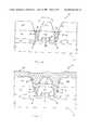
- FIG. 2shows a cross-section of a substrate assembly 30 at an early stage in the fabrication process of the present invention.
- the substrate assembly 30includes a substrate layer 32 , which is the lowest layer of semiconductor material on a wafer, and additional layers or structures formed thereon.
- a LOCOS processis performed to provide a layer of gate oxide 33 separated by field oxide regions 34 .
- a polysilicon layer 36is deposited and etched to provide a contact area, typically for the gate terminal of a transistor.
- a spacer 37may be formed along the layer 36 using conventional techniques. Impurities are diffused into the substrate 34 through suitable masks to form diffusion areas 38 .
- the diffusion areas 38give rise to depletion regions that essentially isolate the source and drain terminals of the transistor from one another by two diodes.
- Silicide layers 40are formed on the diffusion areas 38 .
- the silicide layers 40are formed by depositing a refractory metal such as titanium, platinum, palladium, cobalt, or tungsten on polysilicon. The metal/silicon alloy is then sintered to form the silicide layers 40 .
- the substrate assembly 30is then ready for metallization.
- a layer of photoresist 42is deposited on the substrate assembly 30 and is masked, hardened, and etched to define openings 43 for contact plugs.
- the photoresist layer 42is hardened by baking the substrate assembly 30 at a temperature typically below 100° C.
- FIG. 3shows the substrate assembly 30 of FIG. 2 after a bilayer adhesion promoter layer 44 is deposited by, for example, sputtering onto the surface of the etched photoresist layer 42 . Ionized sputtering is preferred to provide effective coverage of the sidewalls of deep openings. A chemical vapor deposition (CVD) process may also be used to deposit the bilayer adhesion promotor layer 44 .
- the bilayer adhesion promoter layer 44can be, among other substances, titanium/copper, chromium/copper, titanium nitride/copper, or tantalum/copper.
- a metal layer 46is formed by, for example, plating on the bilayer adhesion promoter layer 44 .
- the metal layer 46is preferably copper, which can be electroplated or electroless plated on the substrate assembly 30 at a process temperature around 30° C.
- the metal layer 46may also be deposited using a CVD process.
- the excess metal from the metal layer 46 and the excess bilayer adhesion promoter layer 44are removed through mechanical abrasion, for example, by chemical mechanical polishing, to form metal plugs 48 , as shown in FIG. 5.
- the substrate assembly 30is planar after the removal of the excess metal and the remaining portions of the bilayer adhesion promoter layer 44 define receptacles 45 , in which the metal plugs 48 are located.
- FIG. 7shows a bilayer adhesion promoter layer 52 deposited on the etched photoresist layer 50 and the metal plugs 48 and a first metal layer 54 plated on the bilayer adhesion promoter layer 52 .
- a portion of the metalfills the openings 51 forming contacts 53 .
- Excess metal from the first metal layer 54 and excess bilayer adhesion promoter layer 52are removed by mechanical abrasion, as shown in FIG. 8.
- the first metal layer 54has contacts 53 and the resulting substrate assembly is planar.
- FIG. 9illustrates the substrate assembly 30 of FIG. 8 after photoresist layer 62 is deposited, hardened and etched, bilayer adhesion promoter layer 64 is deposited, and a metal layer is deposited onto the substrate assembly 30 .
- the substrate assembly 30 in FIG. 9has been mechanically polished to remove the excess metal and the remaining portions of the bilayer adhesion promoter layer 64 to form metal plug 66 in receptacle 68 .
- a second metal layer 70has been deposited on the substrate assembly 30 to form contact 72 . Multiple layers of metal can be built up by adding layers of bilayer adhesion promoter, photoresist, and metal.
- FIG. 10shows a resulting substrate assembly 30 of FIG. 9 with the first metal layer 54 and the second metal layer 70 formed.
- the photoresist layers 42 , 50 and 62are removed by, for example, ashing in oxygen plasma to form air gaps 56 .
- the metal layers 54 and 70are supported by columns 60 and 74 formed by the combination of the metal plugs 48 and 66 and the contacts 53 and 72 .
- the air gaps 56have a dielectric constant of 1, thereby reducing the capacitance of the resulting structure. By selecting appropriate metal conductors which have a low resistance, the RC time constant of the resulting structure is reduced.
- the present inventionalso contemplates a method by which the above-described semiconductor interconnect structure is fabricated using typical fabrication steps, materials, and machines.
- the methodin its broadest form, is comprised of the steps of depositing a layer of photoresist on a substrate assembly.
- the photoresistis etched to form openings.
- a metal layeris formed on the photoresist layer so as to fill the openings formed in the photoresist layer. Thereafter, the photoresist layer is removed by, for example, ashing.
- the metal layeris thus supported by the metal which filled the openings formed in the photoresist.
- the method of the present inventionmay be modified by, for example, depositing a promoter layer prior to forming the metal layer.
- Conventional techniquesmay be used for the “depositing” and “forming” steps such as sputtering and electroplating.
- a wide variety of metals and promotersmay be used in the process.
- FIG. 11illustrates a semiconductor device 58 in which the present invention may be employed.
- the semiconductor device 58may be any type of solid state device, such as a memory device.
Landscapes
- Engineering & Computer Science (AREA)
- Physics & Mathematics (AREA)
- Condensed Matter Physics & Semiconductors (AREA)
- General Physics & Mathematics (AREA)
- Computer Hardware Design (AREA)
- Microelectronics & Electronic Packaging (AREA)
- Power Engineering (AREA)
- Manufacturing & Machinery (AREA)
- Internal Circuitry In Semiconductor Integrated Circuit Devices (AREA)
Abstract
Description
- II. CROSS REFERENCE TO RELATED APPLICATIONS[0001]
- (Not Applicable)[0002]
- (Not Applicable)[0003]
- 1. Field of the Invention[0004]
- The present invention is directed generally to semiconductor interconnect layers exhibiting a low RC time delay, and, more particularly, to semiconductor interconnect layers made of a material having a low resistivity that is surrounded by a material with a low dielectric constant.[0005]
- 2. Description of the Background[0006]
- It is common in the semiconductor art to use layers of metal, polysilicon, or another conductor to conduct current between various semiconductor devices that form integrated circuits. The layers of conductor are connected to each other by means of vias and are connected to other materials by means of contacts.[0007]
- When a metal is used to form the interconnect layers of conductors, the metal is usually deposited on the semiconductor by sputtering, chemical vapor deposition (CVD), or evaporation. The CVD process forms a non-volatile solid film on a substrate by the reaction of vapor phase chemicals that contain the desired constituents. The metals that are commonly used for the interconnect layers are aluminum and its alloys. The metal layers are typically deposited over dielectric materials, such as silicon dioxide. Thus, parallel plate capacitive effects are observed due to this structure. The capacitance for a layer can be represented as:[0008]

- where:[0009]
- D=SiO[0010]2thickness
- A=Area of plates[0011]
- ε[0012]0=Permittivity of free space
- ε[0013]ins=Permittivity of SiO2
- where:[0015]
- p=Material resistivity[0016]
- t=Material thickness[0017]
- L=Material length[0018]
- W=Material width[0019]
- Thus, the time delay caused by the product of the line resistance and the capacitance becomes critical.[0020]
- FIG. 1 shows a cross sectional view of a typical semiconductor device (a transistor) in simplified form. A Local Oxidation of Silicon (LOCOS) process is performed on a[0021]
substrate layer 10 to create agate oxide region 12 separated byfield oxide regions 13. Apolysilicon layer 14 is then deposited, typically to form the gate structure of the transistor, and aspacer 15 is fabricated around the remainder oflayer 14. Impurities are diffused into thesubstrate layer 10 to formdiffusion areas 16, which typically form the drain and source structures of the transistor. A layer ofsilicon dioxide 18 is grown and the contact and via areas are removed by etching. A silicide ormetal layer 20 is formed on thediffusion areas 16, which typically provide areas for interconnection with the drain and source structures of the transistor. A first layer ofmetal 22, typically aluminum or an alloy of aluminum, is then deposited and areas are removed to form the required interconnection pattern. Alternatively, metal contact plugs may be formed in the contact and via area formed inlayer 18. Subsequent layers of silicon dioxide and metal may be grown and deposited, respectively, depending on the interconnection pattern required for the integrated circuit. - An attempt to reduce the capacitance associated with interconnect layers deposited on dielectric materials is shown in Togo, et al., “A Gate-side Air-gap Structure (GAS) to Reduce the Parasitic Capacitance in MOSFETs”, 1996 Symposium on VLSI Technology Digest of Technical Papers, pp 38-39. Togo, et al. outlines a transistor structure in which the sidewalls of the gate structure are surrounded by an air gap. A silicon nitride sidewall is first fabricated that surrounds the gate. A layer of silicon dioxide is formed around the silicon nitride sidewall. The silicon nitride sidewall is removed by a wet etching process to form an air gap between the gate structure and the silicon dioxide.[0022]
- Another attempt to reduce the capacitance associated with interconnect layers deposited on silicon is shown in Anand, et al., “NURA: A Feasible, Gas-Dielectric Interconnect Process”, 1996 Symposium on VLSI Technology Digest of Technical Papers, pp. 82-83. Anand, et al. outlines a metal interconnect structure in which layers of a gas are formed between thin layers of silicon dioxide. The thin layers of silicon dioxide have metal interconnect layers deposited on them. The process begins when layers of carbon are formed on a surface and trenches are formed for future interconnections. An interconnect metal layer is formed in the carbon trenches and a thin layer of silicon dioxide is sputter-deposited. Oxygen is then furnace ashed into the carbon layer through diffusion and the oxygen reacts with the carbon to form carbon dioxide. This process is repeated to form the interconnect structure of the device under fabrication.[0023]
- Although Togo, et al. claims to reduce the capacitance associated with the interconnect layers by reducing the dielectric constant of the materials between the interconnect layers, Togo, et al. only provides a low dielectric material (air) around the gate contact of a transistor. Also, Togo, et al. does not disclose an interconnect structure that has reduced resistivity.[0024]
- Likewise, even though Anand, et al. claims to reduce the capacitance associated with the interconnect layers by reducing the dielectric constant of the materials between the interconnect layers, Anand, et al. adds complexity to the semiconductor fabrication process because carbon is used in the process, which is not typically used in the manufacture of semiconductor devices. The method of Anand, et al. does not disclose an interconnect structure that has reduced resistivity.[0025]
- Thus, the need exists for a semiconductor interconnect structure with reduced capacitance and reduced resistivity, thereby decreasing the RC time delay associated with the interconnect layers. The need also exists for a method of fabricating such a structure using standard fabrication steps in conjunction with commercially available processing equipment.[0026]
- The present invention is directed generally to a semiconductor interconnect structure and a method of making the same. Layers of photoresist are formed between conductive layers and the photoresist is removed by, for example, ashing in oxygen plasma. When the photoresist layers are removed, the conductive layers are surrounded by air, which has a dielectric constant of 1. The conductive layers are preferably comprised of copper.[0027]
- The present invention represents significant advantages over the prior art. Because the air spaces between the conductive interconnect layers are formed by removing layers of photoresist, no extra material need be introduced into the semiconductor manufacturing process. Also, because the conductive interconnect layers are surrounded by air, the plate capacitance of the interconnect structure is reduced. Furthermore, because a low resistive material such as copper is used for the conductive interconnect layers, the resistance associated with the interconnect structure is reduced. Using copper as the material for the interconnect layers has the further advantage that the layers may be electroplated or electroless plated at low temperatures. Those advantages and benefits of the present invention, and others, will become apparent from the Detailed Description of the Invention hereinbelow.[0028]
- For the present invention to be clearly understood and readily practiced, the present invention will be described in conjunction with the following figures wherein:[0029]
- FIG. 1 is a cross-sectional view of a typical prior art semiconductor device;[0030]
- FIG. 2 is a cross-sectional view of a substrate assembly on which a layer of photoresist has been deposited, masked, hardened, and etched;[0031]
- FIG. 3 is a cross-sectional view of the substrate assembly of FIG. 2 on which a promoter layer has been deposited on the etched photoresist layer;[0032]
- FIG. 4 is a cross-sectional view of the substrate assembly of FIG. 3 on which a metal layer has been deposited on the promoter layer;[0033]
- FIG. 5 is a cross-sectional view of the substrate assembly of FIG. 4 following removal of excess metal from the metal layer to form metal plugs;[0034]
- FIG. 6 is a cross-sectional view of the substrate assembly of FIG. 5 on which a photoresist layer has been deposited, masked, hardened, and etched on the promoter layer and metal plugs;[0035]
- FIG. 7 is a cross-sectional view of the substrate assembly of FIG. 6 on which a promoter layer and a first metal layer have been deposited on the etched photoresist layer;[0036]
- FIG. 8 is a cross-sectional view of the substrate assembly of FIG. 7 following the removal of excess metal from the first metal layer;[0037]
- FIG. 9 is a cross sectional view of the substrate assembly of FIG. 8 following the addition of a photoresist layer, a bilayer adhesion promoter layer, a metal plug, and a second metal layer onto the etched photoresist layer and the first metal layer;[0038]
- FIG. 10 is a cross-sectional view of the substrate assembly of FIG. 9 following the removal of the photoresist layers to form gaps between the promoter layers and the underlying substrate assembly; and[0039]
- FIG. 11 illustrates a semiconductor device in which the present invention may be used.[0040]
- It is to be understood that the figures have been simplified to illustrate only those aspects of semiconductor topography which are relevant, and some of the dimensions have been exaggerated to convey a clear understanding of the present invention, while eliminating, for the purposes of clarity, some elements normally found on a semiconductor. Those of ordinary skill in the art will recognize that other elements and process steps are required to produce an operational semiconductor. However, because such elements and process steps are well known in the art, and because they do not further aid in the understanding of the present invention, a discussion of such elements is not provided herein.[0041]
- FIG. 2 shows a cross-section of a[0042]
substrate assembly 30 at an early stage in the fabrication process of the present invention. Thesubstrate assembly 30 includes asubstrate layer 32, which is the lowest layer of semiconductor material on a wafer, and additional layers or structures formed thereon. A LOCOS process is performed to provide a layer ofgate oxide 33 separated byfield oxide regions 34. Apolysilicon layer 36 is deposited and etched to provide a contact area, typically for the gate terminal of a transistor. Aspacer 37 may be formed along thelayer 36 using conventional techniques. Impurities are diffused into thesubstrate 34 through suitable masks to formdiffusion areas 38. Thediffusion areas 38 give rise to depletion regions that essentially isolate the source and drain terminals of the transistor from one another by two diodes. Silicide layers40 are formed on thediffusion areas 38. The silicide layers40 are formed by depositing a refractory metal such as titanium, platinum, palladium, cobalt, or tungsten on polysilicon. The metal/silicon alloy is then sintered to form the silicide layers40. - After the silicide layers[0043]40 are formed, the
substrate assembly 30 is then ready for metallization. A layer ofphotoresist 42 is deposited on thesubstrate assembly 30 and is masked, hardened, and etched to defineopenings 43 for contact plugs. Thephotoresist layer 42 is hardened by baking thesubstrate assembly 30 at a temperature typically below 100° C. - FIG. 3 shows the[0044]
substrate assembly 30 of FIG. 2 after a bilayeradhesion promoter layer 44 is deposited by, for example, sputtering onto the surface of the etchedphotoresist layer 42. Ionized sputtering is preferred to provide effective coverage of the sidewalls of deep openings. A chemical vapor deposition (CVD) process may also be used to deposit the bilayeradhesion promotor layer 44. The bilayeradhesion promoter layer 44 can be, among other substances, titanium/copper, chromium/copper, titanium nitride/copper, or tantalum/copper. - As shown in FIG. 4, a[0045]
metal layer 46 is formed by, for example, plating on the bilayeradhesion promoter layer 44. Themetal layer 46 is preferably copper, which can be electroplated or electroless plated on thesubstrate assembly 30 at a process temperature around 30° C. Themetal layer 46 may also be deposited using a CVD process. The excess metal from themetal layer 46 and the excess bilayeradhesion promoter layer 44 are removed through mechanical abrasion, for example, by chemical mechanical polishing, to form metal plugs48, as shown in FIG. 5. Thesubstrate assembly 30 is planar after the removal of the excess metal and the remaining portions of the bilayeradhesion promoter layer 44 definereceptacles 45, in which the metal plugs48 are located. - Another[0046]
photoresist layer 50 is deposited onto the bilayeradhesion promoter layer 44 and the metal plugs48 as shown in FIG. 6. Thephotoresist layer 50 is masked, hardened, and etched to defineopenings 51 for a metal layer which is aligned with theplugs 48. FIG. 7 shows a bilayeradhesion promoter layer 52 deposited on the etchedphotoresist layer 50 and the metal plugs48 and afirst metal layer 54 plated on the bilayeradhesion promoter layer 52. A portion of the metal fills theopenings 51 formingcontacts 53. Excess metal from thefirst metal layer 54 and excess bilayeradhesion promoter layer 52 are removed by mechanical abrasion, as shown in FIG. 8. Thus, thefirst metal layer 54 hascontacts 53 and the resulting substrate assembly is planar. - FIG. 9 illustrates the[0047]
substrate assembly 30 of FIG. 8 afterphotoresist layer 62 is deposited, hardened and etched, bilayeradhesion promoter layer 64 is deposited, and a metal layer is deposited onto thesubstrate assembly 30. Thesubstrate assembly 30 in FIG. 9 has been mechanically polished to remove the excess metal and the remaining portions of the bilayeradhesion promoter layer 64 to formmetal plug 66 inreceptacle 68. Asecond metal layer 70 has been deposited on thesubstrate assembly 30 to formcontact 72. Multiple layers of metal can be built up by adding layers of bilayer adhesion promoter, photoresist, and metal. - FIG. 10 shows a resulting[0048]
substrate assembly 30 of FIG. 9 with thefirst metal layer 54 and thesecond metal layer 70 formed. The photoresist layers42,50 and62 are removed by, for example, ashing in oxygen plasma to formair gaps 56. The metal layers54 and70 are supported bycolumns 60 and74 formed by the combination of the metal plugs48 and66 and thecontacts air gaps 56 have a dielectric constant of 1, thereby reducing the capacitance of the resulting structure. By selecting appropriate metal conductors which have a low resistance, the RC time constant of the resulting structure is reduced. - The present invention also contemplates a method by which the above-described semiconductor interconnect structure is fabricated using typical fabrication steps, materials, and machines. The method, in its broadest form, is comprised of the steps of depositing a layer of photoresist on a substrate assembly. The photoresist is etched to form openings. A metal layer is formed on the photoresist layer so as to fill the openings formed in the photoresist layer. Thereafter, the photoresist layer is removed by, for example, ashing. The metal layer is thus supported by the metal which filled the openings formed in the photoresist.[0049]
- The method of the present invention may be modified by, for example, depositing a promoter layer prior to forming the metal layer. Conventional techniques may be used for the “depositing” and “forming” steps such as sputtering and electroplating. A wide variety of metals and promoters may be used in the process.[0050]
- FIG. 11 illustrates a[0051]
semiconductor device 58 in which the present invention may be employed. Thesemiconductor device 58 may be any type of solid state device, such as a memory device. - While the present invention has been described in conjunction with preferred embodiments thereof, many modifications and variations will be apparent to those of ordinary skill in the art. The foregoing description and the following claims are intended to cover all such modifications and variations.[0052]


Claims (36)
1. A method of fabricating a semiconductor interconnect structure, comprising the steps of:
forming a patterned resist layer on a substrate assembly to define openings;
depositing a metal layer on said resist layer and into said openings; and
removing said resist layer to form a gap between said metal layer and said underlying substrate assembly.
2. The method of
claim 1
3. The method of
claim 2
4. The method of
claim 2
5. The method of
claim 1
6. The method of
claim 1
7. The method of
claim 1
8. The method of
claim 1
9. A method of fabricating a semiconductor interconnect structure, comprising the steps of:
depositing a first photoresist layer on a substrate assembly;
removing certain of said first photoresist layer to form a first set of openings therein;
depositing a first metal layer on said first photoresist layer and into said first set of openings;
removing metal from said metal layer so as to leave metal plugs deposited into said first set of openings;
depositing a second photoresist layer on said first photoresist layer and said metal plugs;
removing certain of said second photoresist layer to form a second set of openings therein, said second set of openings aligned with said metal plugs;
depositing a second metal layer on said second photoresist layer and into said second set of openings; and
removing said first and second photoresist layers such that said second metal layer is supported by said metal plugs and said metal deposited into said second set of openings.
10. The method of
claim 9
11. The method of
claim 10
12. The method of
claim 10
13. The method of
claim 10
14. The method of
claim 11
15. The method of
claim 11
16. The method of
claim 9
17. The method of
claim 9
18. The method of
claim 9
19. The method of
claim 9
20. The method of
claim 9
21. The method of
claim 9
22. The method of
claim 9
23. A semiconductor interconnect structure for a substrate assembly, comprising:
a promoter layer defining openings; and
a metal layer having a portion elevated above said substrate assembly and a portion filling said openings such that said metal layer is in electrical contact with the substrate assembly through said metal filling said openings which metal supports said elevated portion.
24. The semiconductor interconnect structure of
claim 23
25. The semiconductor interconnect structure of
claim 23
26. The semiconductor interconnect structure of
claim 23
27. The semiconductor interconnect structure of
claim 23
28. The semiconductor interconnect structure of
claim 23
29. A semiconductor interconnect structure for a substrate assembly, comprising:
a first promoter layer defining a plurality of receptacles;
a plurality of metal plugs formed in said plurality of receptacles;
a second promoter layer defining a plurality of openings above said metal plugs; and
a metal layer having a portion elevated above said substrate assembly and a portion filling said plurality of openings such that said metal layer is in electrical contact with the substrate assembly, said metal filling said plurality of openings and said plurality of metal plugs supporting said elevated portion of said metal layer.
30. The semiconductor interconnect structure of
claim 29
31. The semiconductor interconnect structure of
claim 29
32. The semiconductor interconnect structure of
claim 29
33. The semiconductor interconnect structure of
claim 29
34. The semiconductor interconnect structure of
claim 29
35. A semiconductor device, comprising:
a substrate assembly; and
at least one interconnect structure, said interconnect structure comprising:
a promoter layer defining receptacles; and
a metal layer having a portion elevated above said substrate assembly and a portion filling said openings such that said metal layer is in electrical contact with the substrate assembly through said metal filling said openings which metal supports said elevated portion.
36. A semiconductor device, comprising:
a substrate assembly; and
at least one interconnect structure, said interconnect structure comprising:
a first promoter layer defining a plurality of receptacles;
a plurality of metal plugs formed in said plurality of receptacles;
a second promoter layer defining a plurality of openings above said metal plugs; and
a metal layer having a portion elevated above said substrate assembly and a portion filling said plurality of openings such that said metal layer is in electrical contact with the substrate assembly, said metal filling said plurality of openings and said plurality of metal plugs supporting said elevated portion of said metal layer.
Priority Applications (2)
| Application Number | Priority Date | Filing Date | Title |
|---|---|---|---|
| US09/325,329US6633074B2 (en) | 1997-06-13 | 1999-06-03 | Integrated circuit wiring with low RC time delay |
| US10/641,540US7271085B2 (en) | 1997-06-13 | 2003-08-15 | Method of fabricating a semiconductor interconnect structure |
Applications Claiming Priority (2)
| Application Number | Priority Date | Filing Date | Title |
|---|---|---|---|
| US08/874,389US6037248A (en) | 1997-06-13 | 1997-06-13 | Method of fabricating integrated circuit wiring with low RC time delay |
| US09/325,329US6633074B2 (en) | 1997-06-13 | 1999-06-03 | Integrated circuit wiring with low RC time delay |
Related Parent Applications (1)
| Application Number | Title | Priority Date | Filing Date |
|---|---|---|---|
| US08/874,389DivisionUS6037248A (en) | 1997-06-13 | 1997-06-13 | Method of fabricating integrated circuit wiring with low RC time delay |
Related Child Applications (1)
| Application Number | Title | Priority Date | Filing Date |
|---|---|---|---|
| US10/641,540ContinuationUS7271085B2 (en) | 1997-06-13 | 2003-08-15 | Method of fabricating a semiconductor interconnect structure |
Publications (2)
| Publication Number | Publication Date |
|---|---|
| US20010015494A1true US20010015494A1 (en) | 2001-08-23 |
| US6633074B2 US6633074B2 (en) | 2003-10-14 |
Family
ID=25363634
Family Applications (3)
| Application Number | Title | Priority Date | Filing Date |
|---|---|---|---|
| US08/874,389Expired - LifetimeUS6037248A (en) | 1997-06-13 | 1997-06-13 | Method of fabricating integrated circuit wiring with low RC time delay |
| US09/325,329Expired - Fee RelatedUS6633074B2 (en) | 1997-06-13 | 1999-06-03 | Integrated circuit wiring with low RC time delay |
| US10/641,540Expired - Fee RelatedUS7271085B2 (en) | 1997-06-13 | 2003-08-15 | Method of fabricating a semiconductor interconnect structure |
Family Applications Before (1)
| Application Number | Title | Priority Date | Filing Date |
|---|---|---|---|
| US08/874,389Expired - LifetimeUS6037248A (en) | 1997-06-13 | 1997-06-13 | Method of fabricating integrated circuit wiring with low RC time delay |
Family Applications After (1)
| Application Number | Title | Priority Date | Filing Date |
|---|---|---|---|
| US10/641,540Expired - Fee RelatedUS7271085B2 (en) | 1997-06-13 | 2003-08-15 | Method of fabricating a semiconductor interconnect structure |
Country Status (1)
| Country | Link |
|---|---|
| US (3) | US6037248A (en) |
Cited By (38)
| Publication number | Priority date | Publication date | Assignee | Title |
|---|---|---|---|---|
| US20040202786A1 (en)* | 2001-05-22 | 2004-10-14 | Novellus Systems, Inc. | Method of forming low-resistivity tungsten interconnects |
| US20050031786A1 (en)* | 2001-05-22 | 2005-02-10 | Novellus Systems, Inc. | Method for reducing tungsten film roughness and improving step coverage |
| US20060094238A1 (en)* | 2003-01-21 | 2006-05-04 | Novellus Systems, Inc. | Deposition of tungsten nitride |
| US7157798B1 (en)* | 2003-05-09 | 2007-01-02 | Novellus Systems, Inc. | Selective refractory metal and nitride capping |
| US20080045010A1 (en)* | 2003-08-26 | 2008-02-21 | Novellus Systems, Inc. | Reducing silicon attack and improving resistivity of tungsten nitride film |
| US20080124926A1 (en)* | 2001-05-22 | 2008-05-29 | Novellus Systems, Inc. | Methods for growing low-resistivity tungsten film |
| US20090114832A1 (en)* | 2007-08-30 | 2009-05-07 | Kelvin Lynn | Semiconductive materials and associated uses thereof |
| US20090149022A1 (en)* | 2007-12-05 | 2009-06-11 | Novellus Systems, Inc. | Method for improving uniformity and adhesion of low resistivity tungsten film |
| US20090163025A1 (en)* | 2007-12-21 | 2009-06-25 | Novellus Systems, Inc. | Methods for forming all tungsten contacts and lines |
| US7655567B1 (en) | 2007-07-24 | 2010-02-02 | Novellus Systems, Inc. | Methods for improving uniformity and resistivity of thin tungsten films |
| US20100055904A1 (en)* | 2008-08-29 | 2010-03-04 | Novellus Systems Inc. | Method for reducing tungsten roughness and improving reflectivity |
| US20100159694A1 (en)* | 2008-06-12 | 2010-06-24 | Novellus Systems Inc. | Method for depositing thin tungsten film with low resistivity and robust micro-adhesion characteristics |
| US20100267235A1 (en)* | 2009-04-16 | 2010-10-21 | Feng Chen | Methods for depositing ultra thin low resistivity tungsten film for small critical dimension contacts and interconnects |
| US20110059608A1 (en)* | 2009-09-09 | 2011-03-10 | Novellus Systems, Inc. | Method for improving adhesion of low resistivity tungsten/tungsten nitride layers |
| US7955972B2 (en) | 2001-05-22 | 2011-06-07 | Novellus Systems, Inc. | Methods for growing low-resistivity tungsten for high aspect ratio and small features |
| US8062977B1 (en) | 2008-01-31 | 2011-11-22 | Novellus Systems, Inc. | Ternary tungsten-containing resistive thin films |
| US8709948B2 (en) | 2010-03-12 | 2014-04-29 | Novellus Systems, Inc. | Tungsten barrier and seed for copper filled TSV |
| US8853080B2 (en) | 2012-09-09 | 2014-10-07 | Novellus Systems, Inc. | Method for depositing tungsten film with low roughness and low resistivity |
| US8975184B2 (en) | 2012-07-27 | 2015-03-10 | Novellus Systems, Inc. | Methods of improving tungsten contact resistance in small critical dimension features |
| US9034760B2 (en) | 2012-06-29 | 2015-05-19 | Novellus Systems, Inc. | Methods of forming tensile tungsten films and compressive tungsten films |
| US9076843B2 (en) | 2001-05-22 | 2015-07-07 | Novellus Systems, Inc. | Method for producing ultra-thin tungsten layers with improved step coverage |
| US9153486B2 (en) | 2013-04-12 | 2015-10-06 | Lam Research Corporation | CVD based metal/semiconductor OHMIC contact for high volume manufacturing applications |
| US9159571B2 (en) | 2009-04-16 | 2015-10-13 | Lam Research Corporation | Tungsten deposition process using germanium-containing reducing agent |
| US9240347B2 (en) | 2012-03-27 | 2016-01-19 | Novellus Systems, Inc. | Tungsten feature fill |
| US9589808B2 (en) | 2013-12-19 | 2017-03-07 | Lam Research Corporation | Method for depositing extremely low resistivity tungsten |
| US9613818B2 (en) | 2015-05-27 | 2017-04-04 | Lam Research Corporation | Deposition of low fluorine tungsten by sequential CVD process |
| US9754824B2 (en) | 2015-05-27 | 2017-09-05 | Lam Research Corporation | Tungsten films having low fluorine content |
| US9953984B2 (en) | 2015-02-11 | 2018-04-24 | Lam Research Corporation | Tungsten for wordline applications |
| US9978605B2 (en) | 2015-05-27 | 2018-05-22 | Lam Research Corporation | Method of forming low resistivity fluorine free tungsten film without nucleation |
| US9997405B2 (en) | 2014-09-30 | 2018-06-12 | Lam Research Corporation | Feature fill with nucleation inhibition |
| US10256142B2 (en) | 2009-08-04 | 2019-04-09 | Novellus Systems, Inc. | Tungsten feature fill with nucleation inhibition |
| US11348795B2 (en) | 2017-08-14 | 2022-05-31 | Lam Research Corporation | Metal fill process for three-dimensional vertical NAND wordline |
| US11549175B2 (en) | 2018-05-03 | 2023-01-10 | Lam Research Corporation | Method of depositing tungsten and other metals in 3D NAND structures |
| US11972952B2 (en) | 2018-12-14 | 2024-04-30 | Lam Research Corporation | Atomic layer deposition on 3D NAND structures |
| US12002679B2 (en) | 2019-04-11 | 2024-06-04 | Lam Research Corporation | High step coverage tungsten deposition |
| US12077858B2 (en) | 2019-08-12 | 2024-09-03 | Lam Research Corporation | Tungsten deposition |
| US12237221B2 (en) | 2019-05-22 | 2025-02-25 | Lam Research Corporation | Nucleation-free tungsten deposition |
| US12444651B2 (en) | 2022-06-28 | 2025-10-14 | Novellus Systems, Inc. | Tungsten feature fill with nucleation inhibition |
Families Citing this family (72)
| Publication number | Priority date | Publication date | Assignee | Title |
|---|---|---|---|---|
| US6429120B1 (en)* | 2000-01-18 | 2002-08-06 | Micron Technology, Inc. | Methods and apparatus for making integrated-circuit wiring from copper, silver, gold, and other metals |
| US6037248A (en)* | 1997-06-13 | 2000-03-14 | Micron Technology, Inc. | Method of fabricating integrated circuit wiring with low RC time delay |
| US6294455B1 (en) | 1997-08-20 | 2001-09-25 | Micron Technology, Inc. | Conductive lines, coaxial lines, integrated circuitry, and methods of forming conductive lines, coaxial lines, and integrated circuitry |
| US6187677B1 (en) | 1997-08-22 | 2001-02-13 | Micron Technology, Inc. | Integrated circuitry and methods of forming integrated circuitry |
| US6143616A (en) | 1997-08-22 | 2000-11-07 | Micron Technology, Inc. | Methods of forming coaxial integrated circuitry interconnect lines |
| US6268261B1 (en)* | 1998-11-03 | 2001-07-31 | International Business Machines Corporation | Microprocessor having air as a dielectric and encapsulated lines and process for manufacture |
| JP2000150647A (en)* | 1998-11-11 | 2000-05-30 | Sony Corp | Wiring structure and its manufacture |
| US6667552B1 (en)* | 1999-02-18 | 2003-12-23 | Advanced Micro Devices, Inc. | Low dielectric metal silicide lined interconnection system |
| US6218282B1 (en)* | 1999-02-18 | 2001-04-17 | Advanced Micro Devices, Inc. | Method of forming low dielectric tungsten lined interconnection system |
| US6245658B1 (en) | 1999-02-18 | 2001-06-12 | Advanced Micro Devices, Inc. | Method of forming low dielectric semiconductor device with rigid, metal silicide lined interconnection system |
| US6246118B1 (en)* | 1999-02-18 | 2001-06-12 | Advanced Micro Devices, Inc. | Low dielectric semiconductor device with rigid, conductively lined interconnection system |
| US6524974B1 (en) | 1999-03-22 | 2003-02-25 | Lsi Logic Corporation | Formation of improved low dielectric constant carbon-containing silicon oxide dielectric material by reaction of carbon-containing silane with oxidizing agent in the presence of one or more reaction retardants |
| US6303047B1 (en) | 1999-03-22 | 2001-10-16 | Lsi Logic Corporation | Low dielectric constant multiple carbon-containing silicon oxide dielectric material for use in integrated circuit structures, and method of making same |
| US6413854B1 (en)* | 1999-08-24 | 2002-07-02 | International Business Machines Corp. | Method to build multi level structure |
| US7105420B1 (en)* | 1999-10-07 | 2006-09-12 | Chartered Semiconductor Manufacturing Ltd. | Method to fabricate horizontal air columns underneath metal inductor |
| US6391795B1 (en) | 1999-10-22 | 2002-05-21 | Lsi Logic Corporation | Low k dielectric composite layer for intergrated circuit structure which provides void-free low k dielectric material between metal lines while mitigating via poisoning |
| US6756674B1 (en)* | 1999-10-22 | 2004-06-29 | Lsi Logic Corporation | Low dielectric constant silicon oxide-based dielectric layer for integrated circuit structures having improved compatibility with via filler materials, and method of making same |
| US6423628B1 (en) | 1999-10-22 | 2002-07-23 | Lsi Logic Corporation | Method of forming integrated circuit structure having low dielectric constant material and having silicon oxynitride caps over closely spaced apart metal lines |
| US6316354B1 (en) | 1999-10-26 | 2001-11-13 | Lsi Logic Corporation | Process for removing resist mask of integrated circuit structure which mitigates damage to underlying low dielectric constant silicon oxide dielectric layer |
| US6383821B1 (en)* | 1999-10-29 | 2002-05-07 | Conexant Systems, Inc. | Semiconductor device and process |
| US7211512B1 (en)* | 2000-01-18 | 2007-05-01 | Micron Technology, Inc. | Selective electroless-plated copper metallization |
| US6420262B1 (en) | 2000-01-18 | 2002-07-16 | Micron Technology, Inc. | Structures and methods to enhance copper metallization |
| US6376370B1 (en)* | 2000-01-18 | 2002-04-23 | Micron Technology, Inc. | Process for providing seed layers for using aluminum, copper, gold and silver metallurgy process for providing seed layers for using aluminum, copper, gold and silver metallurgy |
| US7262130B1 (en)* | 2000-01-18 | 2007-08-28 | Micron Technology, Inc. | Methods for making integrated-circuit wiring from copper, silver, gold, and other metals |
| US6346490B1 (en) | 2000-04-05 | 2002-02-12 | Lsi Logic Corporation | Process for treating damaged surfaces of low k carbon doped silicon oxide dielectric material after plasma etching and plasma cleaning steps |
| US6506678B1 (en) | 2000-05-19 | 2003-01-14 | Lsi Logic Corporation | Integrated circuit structures having low k porous aluminum oxide dielectric material separating aluminum lines, and method of making same |
| US6423629B1 (en)* | 2000-05-31 | 2002-07-23 | Kie Y. Ahn | Multilevel copper interconnects with low-k dielectrics and air gaps |
| US6674167B1 (en)* | 2000-05-31 | 2004-01-06 | Micron Technology, Inc. | Multilevel copper interconnect with double passivation |
| US6365528B1 (en) | 2000-06-07 | 2002-04-02 | Lsi Logic Corporation | Low temperature process for forming a low dielectric constant fluorine and carbon-containing silicon oxide dielectric-material characterized by improved resistance to oxidation and good gap-filling capabilities |
| US6346488B1 (en) | 2000-06-27 | 2002-02-12 | Lsi Logic Corporation | Process to provide enhanced resistance to cracking and to further reduce the dielectric constant of a low dielectric constant dielectric film of an integrated circuit structure by implantation with hydrogen ions |
| US6492731B1 (en) | 2000-06-27 | 2002-12-10 | Lsi Logic Corporation | Composite low dielectric constant film for integrated circuit structure |
| US6368979B1 (en) | 2000-06-28 | 2002-04-09 | Lsi Logic Corporation | Process for forming trenches and vias in layers of low dielectric constant carbon-doped silicon oxide dielectric material of an integrated circuit structure |
| US6350700B1 (en) | 2000-06-28 | 2002-02-26 | Lsi Logic Corporation | Process for forming trenches and vias in layers of low dielectric constant carbon-doped silicon oxide dielectric material of an integrated circuit structure |
| US6368952B1 (en)* | 2000-08-15 | 2002-04-09 | Taiwan Semiconductor Manufacturing Company, Ltd | Diffusion inhibited dielectric structure for diffusion enhanced conductor layer |
| US6489242B1 (en) | 2000-09-13 | 2002-12-03 | Lsi Logic Corporation | Process for planarization of integrated circuit structure which inhibits cracking of low dielectric constant dielectric material adjacent underlying raised structures |
| US6391768B1 (en) | 2000-10-30 | 2002-05-21 | Lsi Logic Corporation | Process for CMP removal of excess trench or via filler metal which inhibits formation of concave regions on oxide surface of integrated circuit structure |
| US6423630B1 (en) | 2000-10-31 | 2002-07-23 | Lsi Logic Corporation | Process for forming low K dielectric material between metal lines |
| US6537923B1 (en) | 2000-10-31 | 2003-03-25 | Lsi Logic Corporation | Process for forming integrated circuit structure with low dielectric constant material between closely spaced apart metal lines |
| US6420277B1 (en) | 2000-11-01 | 2002-07-16 | Lsi Logic Corporation | Process for inhibiting crack formation in low dielectric constant dielectric films of integrated circuit structure |
| US6572925B2 (en) | 2001-02-23 | 2003-06-03 | Lsi Logic Corporation | Process for forming a low dielectric constant fluorine and carbon containing silicon oxide dielectric material |
| US6858195B2 (en) | 2001-02-23 | 2005-02-22 | Lsi Logic Corporation | Process for forming a low dielectric constant fluorine and carbon-containing silicon oxide dielectric material |
| US6649219B2 (en) | 2001-02-23 | 2003-11-18 | Lsi Logic Corporation | Process for forming a low dielectric constant fluorine and carbon-containing silicon oxide dielectric material characterized by improved resistance to oxidation |
| US6696360B2 (en)* | 2001-03-15 | 2004-02-24 | Micron Technology, Inc. | Barrier-metal-free copper damascene technology using atomic hydrogen enhanced reflow |
| US6503840B2 (en) | 2001-05-02 | 2003-01-07 | Lsi Logic Corporation | Process for forming metal-filled openings in low dielectric constant dielectric material while inhibiting via poisoning |
| US6649517B2 (en)* | 2001-05-18 | 2003-11-18 | Chartered Semiconductor Manufacturing Ltd. | Copper metal structure for the reduction of intra-metal capacitance |
| US6559048B1 (en) | 2001-05-30 | 2003-05-06 | Lsi Logic Corporation | Method of making a sloped sidewall via for integrated circuit structure to suppress via poisoning |
| US6583026B1 (en) | 2001-05-31 | 2003-06-24 | Lsi Logic Corporation | Process for forming a low k carbon-doped silicon oxide dielectric material on an integrated circuit structure |
| US6562700B1 (en) | 2001-05-31 | 2003-05-13 | Lsi Logic Corporation | Process for removal of resist mask over low k carbon-doped silicon oxide dielectric material of an integrated circuit structure, and removal of residues from via etch and resist mask removal |
| US6566171B1 (en) | 2001-06-12 | 2003-05-20 | Lsi Logic Corporation | Fuse construction for integrated circuit structure having low dielectric constant dielectric material |
| US6930056B1 (en)* | 2001-06-19 | 2005-08-16 | Lsi Logic Corporation | Plasma treatment of low dielectric constant dielectric material to form structures useful in formation of metal interconnects and/or filled vias for integrated circuit structure |
| US6559033B1 (en) | 2001-06-27 | 2003-05-06 | Lsi Logic Corporation | Processing for forming integrated circuit structure with low dielectric constant material between closely spaced apart metal lines |
| US6673721B1 (en)* | 2001-07-02 | 2004-01-06 | Lsi Logic Corporation | Process for removal of photoresist mask used for making vias in low k carbon-doped silicon oxide dielectric material, and for removal of etch residues from formation of vias and removal of photoresist mask |
| US6940142B2 (en)* | 2001-07-02 | 2005-09-06 | Xerox Corporation | Low data line capacitance image sensor array using air-gap metal crossover |
| US20030008243A1 (en)* | 2001-07-09 | 2003-01-09 | Micron Technology, Inc. | Copper electroless deposition technology for ULSI metalization |
| US6723653B1 (en) | 2001-08-17 | 2004-04-20 | Lsi Logic Corporation | Process for reducing defects in copper-filled vias and/or trenches formed in porous low-k dielectric material |
| US6881664B2 (en)* | 2001-08-28 | 2005-04-19 | Lsi Logic Corporation | Process for planarizing upper surface of damascene wiring structure for integrated circuit structures |
| US7029963B2 (en)* | 2001-08-30 | 2006-04-18 | Micron Technology, Inc. | Semiconductor damascene trench and methods thereof |
| US6528423B1 (en) | 2001-10-26 | 2003-03-04 | Lsi Logic Corporation | Process for forming composite of barrier layers of dielectric material to inhibit migration of copper from copper metal interconnect of integrated circuit structure into adjacent layer of low k dielectric material |
| US6613665B1 (en) | 2001-10-26 | 2003-09-02 | Lsi Logic Corporation | Process for forming integrated circuit structure comprising layer of low k dielectric material having antireflective properties in an upper surface |
| US7220665B2 (en) | 2003-08-05 | 2007-05-22 | Micron Technology, Inc. | H2 plasma treatment |
| US7538024B2 (en)* | 2005-05-03 | 2009-05-26 | United Microelectronics Corp. | Method of fabricating a dual-damascene copper structure |
| US8258057B2 (en)* | 2006-03-30 | 2012-09-04 | Intel Corporation | Copper-filled trench contact for transistor performance improvement |
| US7608538B2 (en) | 2007-01-05 | 2009-10-27 | International Business Machines Corporation | Formation of vertical devices by electroplating |
| FR2911432A1 (en)* | 2007-01-11 | 2008-07-18 | Stmicroelectronics Crolles Sas | Integrated electronic circuit for use in electronic card, has insulating layer including two insulating zones at level of interconnections or level of contacts, where zones are made of different materials |
| US8022543B2 (en)* | 2008-03-25 | 2011-09-20 | International Business Machines Corporation | Underbump metallurgy for enhanced electromigration resistance |
| US8105937B2 (en)* | 2008-08-13 | 2012-01-31 | International Business Machines Corporation | Conformal adhesion promoter liner for metal interconnects |
| JP5185019B2 (en)* | 2008-08-25 | 2013-04-17 | パナソニック株式会社 | Semiconductor device and electronic apparatus using the same |
| US8497203B2 (en) | 2010-08-13 | 2013-07-30 | International Business Machines Corporation | Semiconductor structures and methods of manufacture |
| US9489905B2 (en)* | 2012-02-06 | 2016-11-08 | Himax Technologies Limited | Display device driving method |
| US20130341762A1 (en)* | 2012-06-20 | 2013-12-26 | Macronix International Co., Ltd. | Semiconductor hole structure |
| US9455178B2 (en)* | 2014-03-14 | 2016-09-27 | Taiwan Semiconductor Manufacturing Company, Ltd. | Method of semiconductor integrated circuit fabrication |
| US11101175B2 (en)* | 2018-11-21 | 2021-08-24 | International Business Machines Corporation | Tall trenches for via chamferless and self forming barrier |
Family Cites Families (24)
| Publication number | Priority date | Publication date | Assignee | Title |
|---|---|---|---|---|
| US4753896A (en)* | 1986-11-21 | 1988-06-28 | Texas Instruments Incorporated | Sidewall channel stop process |
| JPH02220464A (en)* | 1989-02-22 | 1990-09-03 | Toshiba Corp | Semiconductor device and its manufacturing method |
| EP0393635B1 (en)* | 1989-04-21 | 1997-09-03 | Nec Corporation | Semiconductor device having multi-level wirings |
| US5000818A (en)* | 1989-08-14 | 1991-03-19 | Fairchild Semiconductor Corporation | Method of fabricating a high performance interconnect system for an integrated circuit |
| US5071518A (en)* | 1989-10-24 | 1991-12-10 | Microelectronics And Computer Technology Corporation | Method of making an electrical multilayer interconnect |
| GB2247986A (en)* | 1990-09-12 | 1992-03-18 | Marconi Gec Ltd | Reducing interconnection capacitance in integrated circuits |
| US5281769A (en)* | 1990-11-05 | 1994-01-25 | Nippon Telegraph And Telephone Corporation | Dewall plating technique |
| JP2731040B2 (en)* | 1991-02-05 | 1998-03-25 | 三菱電機株式会社 | Method for manufacturing semiconductor device |
| CA2082771C (en)* | 1992-11-12 | 1998-02-10 | Vu Quoc Ho | Method for forming interconnect structures for integrated circuits |
| EP0690494B1 (en)* | 1994-06-27 | 2004-03-17 | Infineon Technologies AG | Connection and build-up-process for multi-chip-modules |
| JP2985692B2 (en)* | 1994-11-16 | 1999-12-06 | 日本電気株式会社 | Semiconductor device wiring structure and method of manufacturing the same |
| US5521121A (en)* | 1995-04-03 | 1996-05-28 | Taiwan Semiconductor Manufacturing Company | Oxygen plasma etch process post contact layer etch back |
| JPH09116015A (en)* | 1995-09-15 | 1997-05-02 | Korea Electron Telecommun | Filling method for contact hole |
| US5834845A (en)* | 1995-09-21 | 1998-11-10 | Advanced Micro Devices, Inc. | Interconnect scheme for integrated circuits |
| US5824599A (en)* | 1996-01-16 | 1998-10-20 | Cornell Research Foundation, Inc. | Protected encapsulation of catalytic layer for electroless copper interconnect |
| US6057224A (en)* | 1996-03-29 | 2000-05-02 | Vlsi Technology, Inc. | Methods for making semiconductor devices having air dielectric interconnect structures |
| US5953626A (en)* | 1996-06-05 | 1999-09-14 | Advanced Micro Devices, Inc. | Dissolvable dielectric method |
| US5783864A (en)* | 1996-06-05 | 1998-07-21 | Advanced Micro Devices, Inc. | Multilevel interconnect structure of an integrated circuit having air gaps and pillars separating levels of interconnect |
| US5950102A (en)* | 1997-02-03 | 1999-09-07 | Industrial Technology Research Institute | Method for fabricating air-insulated multilevel metal interconnections for integrated circuits |
| US5935868A (en)* | 1997-03-31 | 1999-08-10 | Intel Corporation | Interconnect structure and method to achieve unlanded vias for low dielectric constant materials |
| US5981374A (en)* | 1997-04-29 | 1999-11-09 | International Business Machines Corporation | Sub-half-micron multi-level interconnection structure and process thereof |
| US6069068A (en)* | 1997-05-30 | 2000-05-30 | International Business Machines Corporation | Sub-quarter-micron copper interconnections with improved electromigration resistance and reduced defect sensitivity |
| US6130161A (en)* | 1997-05-30 | 2000-10-10 | International Business Machines Corporation | Method of forming copper interconnections with enhanced electromigration resistance and reduced defect sensitivity |
| US6037248A (en) | 1997-06-13 | 2000-03-14 | Micron Technology, Inc. | Method of fabricating integrated circuit wiring with low RC time delay |
- 1997
- 1997-06-13USUS08/874,389patent/US6037248A/ennot_activeExpired - Lifetime
- 1999
- 1999-06-03USUS09/325,329patent/US6633074B2/ennot_activeExpired - Fee Related
- 2003
- 2003-08-15USUS10/641,540patent/US7271085B2/ennot_activeExpired - Fee Related
Cited By (65)
| Publication number | Priority date | Publication date | Assignee | Title |
|---|---|---|---|---|
| US8048805B2 (en) | 2001-05-22 | 2011-11-01 | Novellus Systems, Inc. | Methods for growing low-resistivity tungsten film |
| US9583385B2 (en) | 2001-05-22 | 2017-02-28 | Novellus Systems, Inc. | Method for producing ultra-thin tungsten layers with improved step coverage |
| US8409985B2 (en) | 2001-05-22 | 2013-04-02 | Novellus Systems, Inc. | Methods for growing low-resistivity tungsten for high aspect ratio and small features |
| US7141494B2 (en) | 2001-05-22 | 2006-11-28 | Novellus Systems, Inc. | Method for reducing tungsten film roughness and improving step coverage |
| US9076843B2 (en) | 2001-05-22 | 2015-07-07 | Novellus Systems, Inc. | Method for producing ultra-thin tungsten layers with improved step coverage |
| US7262125B2 (en) | 2001-05-22 | 2007-08-28 | Novellus Systems, Inc. | Method of forming low-resistivity tungsten interconnects |
| US20100035427A1 (en)* | 2001-05-22 | 2010-02-11 | Novellus Systems, Inc. | Methods for growing low-resistivity tungsten film |
| US20080124926A1 (en)* | 2001-05-22 | 2008-05-29 | Novellus Systems, Inc. | Methods for growing low-resistivity tungsten film |
| US20050031786A1 (en)* | 2001-05-22 | 2005-02-10 | Novellus Systems, Inc. | Method for reducing tungsten film roughness and improving step coverage |
| US20110223763A1 (en)* | 2001-05-22 | 2011-09-15 | Lana Hiului Chan | Methods for growing low-resistivity tungsten for high aspect ratio and small features |
| US7955972B2 (en) | 2001-05-22 | 2011-06-07 | Novellus Systems, Inc. | Methods for growing low-resistivity tungsten for high aspect ratio and small features |
| US7589017B2 (en) | 2001-05-22 | 2009-09-15 | Novellus Systems, Inc. | Methods for growing low-resistivity tungsten film |
| US20040202786A1 (en)* | 2001-05-22 | 2004-10-14 | Novellus Systems, Inc. | Method of forming low-resistivity tungsten interconnects |
| US7691749B2 (en) | 2003-01-21 | 2010-04-06 | Novellus Systems, Inc. | Deposition of tungsten nitride |
| US20060094238A1 (en)* | 2003-01-21 | 2006-05-04 | Novellus Systems, Inc. | Deposition of tungsten nitride |
| US7157798B1 (en)* | 2003-05-09 | 2007-01-02 | Novellus Systems, Inc. | Selective refractory metal and nitride capping |
| US20080045010A1 (en)* | 2003-08-26 | 2008-02-21 | Novellus Systems, Inc. | Reducing silicon attack and improving resistivity of tungsten nitride film |
| US7754604B2 (en) | 2003-08-26 | 2010-07-13 | Novellus Systems, Inc. | Reducing silicon attack and improving resistivity of tungsten nitride film |
| US7655567B1 (en) | 2007-07-24 | 2010-02-02 | Novellus Systems, Inc. | Methods for improving uniformity and resistivity of thin tungsten films |
| US8101521B1 (en) | 2007-07-24 | 2012-01-24 | Novellus Systems, Inc. | Methods for improving uniformity and resistivity of thin tungsten films |
| US20090114832A1 (en)* | 2007-08-30 | 2009-05-07 | Kelvin Lynn | Semiconductive materials and associated uses thereof |
| US7772114B2 (en) | 2007-12-05 | 2010-08-10 | Novellus Systems, Inc. | Method for improving uniformity and adhesion of low resistivity tungsten film |
| US8329576B2 (en) | 2007-12-05 | 2012-12-11 | Novellus Systems, Inc. | Method for improving uniformity and adhesion of low resistivity tungsten film |
| US20090149022A1 (en)* | 2007-12-05 | 2009-06-11 | Novellus Systems, Inc. | Method for improving uniformity and adhesion of low resistivity tungsten film |
| US8367546B2 (en) | 2007-12-21 | 2013-02-05 | Novellus Systems, Inc. | Methods for forming all tungsten contacts and lines |
| US20090163025A1 (en)* | 2007-12-21 | 2009-06-25 | Novellus Systems, Inc. | Methods for forming all tungsten contacts and lines |
| US8053365B2 (en) | 2007-12-21 | 2011-11-08 | Novellus Systems, Inc. | Methods for forming all tungsten contacts and lines |
| US8062977B1 (en) | 2008-01-31 | 2011-11-22 | Novellus Systems, Inc. | Ternary tungsten-containing resistive thin films |
| US20100159694A1 (en)* | 2008-06-12 | 2010-06-24 | Novellus Systems Inc. | Method for depositing thin tungsten film with low resistivity and robust micro-adhesion characteristics |
| US8058170B2 (en) | 2008-06-12 | 2011-11-15 | Novellus Systems, Inc. | Method for depositing thin tungsten film with low resistivity and robust micro-adhesion characteristics |
| US8409987B2 (en) | 2008-06-12 | 2013-04-02 | Novellus Systems, Inc. | Method for depositing thin tungsten film with low resistivity and robust micro-adhesion characteristics |
| US20100055904A1 (en)* | 2008-08-29 | 2010-03-04 | Novellus Systems Inc. | Method for reducing tungsten roughness and improving reflectivity |
| US8551885B2 (en) | 2008-08-29 | 2013-10-08 | Novellus Systems, Inc. | Method for reducing tungsten roughness and improving reflectivity |
| US8623733B2 (en) | 2009-04-16 | 2014-01-07 | Novellus Systems, Inc. | Methods for depositing ultra thin low resistivity tungsten film for small critical dimension contacts and interconnects |
| US9159571B2 (en) | 2009-04-16 | 2015-10-13 | Lam Research Corporation | Tungsten deposition process using germanium-containing reducing agent |
| US20100267230A1 (en)* | 2009-04-16 | 2010-10-21 | Anand Chandrashekar | Method for forming tungsten contacts and interconnects with small critical dimensions |
| US20100267235A1 (en)* | 2009-04-16 | 2010-10-21 | Feng Chen | Methods for depositing ultra thin low resistivity tungsten film for small critical dimension contacts and interconnects |
| US9673146B2 (en) | 2009-04-16 | 2017-06-06 | Novellus Systems, Inc. | Low temperature tungsten film deposition for small critical dimension contacts and interconnects |
| US9236297B2 (en) | 2009-04-16 | 2016-01-12 | Novellus Systems, Inc. | Low tempature tungsten film deposition for small critical dimension contacts and interconnects |
| US10256142B2 (en) | 2009-08-04 | 2019-04-09 | Novellus Systems, Inc. | Tungsten feature fill with nucleation inhibition |
| US9653353B2 (en) | 2009-08-04 | 2017-05-16 | Novellus Systems, Inc. | Tungsten feature fill |
| US10103058B2 (en) | 2009-08-04 | 2018-10-16 | Novellus Systems, Inc. | Tungsten feature fill |
| US8207062B2 (en) | 2009-09-09 | 2012-06-26 | Novellus Systems, Inc. | Method for improving adhesion of low resistivity tungsten/tungsten nitride layers |
| US20110059608A1 (en)* | 2009-09-09 | 2011-03-10 | Novellus Systems, Inc. | Method for improving adhesion of low resistivity tungsten/tungsten nitride layers |
| US8709948B2 (en) | 2010-03-12 | 2014-04-29 | Novellus Systems, Inc. | Tungsten barrier and seed for copper filled TSV |
| US9240347B2 (en) | 2012-03-27 | 2016-01-19 | Novellus Systems, Inc. | Tungsten feature fill |
| US9034760B2 (en) | 2012-06-29 | 2015-05-19 | Novellus Systems, Inc. | Methods of forming tensile tungsten films and compressive tungsten films |
| US8975184B2 (en) | 2012-07-27 | 2015-03-10 | Novellus Systems, Inc. | Methods of improving tungsten contact resistance in small critical dimension features |
| US8853080B2 (en) | 2012-09-09 | 2014-10-07 | Novellus Systems, Inc. | Method for depositing tungsten film with low roughness and low resistivity |
| US9153486B2 (en) | 2013-04-12 | 2015-10-06 | Lam Research Corporation | CVD based metal/semiconductor OHMIC contact for high volume manufacturing applications |
| US9589808B2 (en) | 2013-12-19 | 2017-03-07 | Lam Research Corporation | Method for depositing extremely low resistivity tungsten |
| US9997405B2 (en) | 2014-09-30 | 2018-06-12 | Lam Research Corporation | Feature fill with nucleation inhibition |
| US10529722B2 (en) | 2015-02-11 | 2020-01-07 | Lam Research Corporation | Tungsten for wordline applications |
| US9953984B2 (en) | 2015-02-11 | 2018-04-24 | Lam Research Corporation | Tungsten for wordline applications |
| US9978605B2 (en) | 2015-05-27 | 2018-05-22 | Lam Research Corporation | Method of forming low resistivity fluorine free tungsten film without nucleation |
| US9754824B2 (en) | 2015-05-27 | 2017-09-05 | Lam Research Corporation | Tungsten films having low fluorine content |
| US9613818B2 (en) | 2015-05-27 | 2017-04-04 | Lam Research Corporation | Deposition of low fluorine tungsten by sequential CVD process |
| US10546751B2 (en) | 2015-05-27 | 2020-01-28 | Lam Research Corporation | Forming low resistivity fluorine free tungsten film without nucleation |
| US11348795B2 (en) | 2017-08-14 | 2022-05-31 | Lam Research Corporation | Metal fill process for three-dimensional vertical NAND wordline |
| US11549175B2 (en) | 2018-05-03 | 2023-01-10 | Lam Research Corporation | Method of depositing tungsten and other metals in 3D NAND structures |
| US11972952B2 (en) | 2018-12-14 | 2024-04-30 | Lam Research Corporation | Atomic layer deposition on 3D NAND structures |
| US12002679B2 (en) | 2019-04-11 | 2024-06-04 | Lam Research Corporation | High step coverage tungsten deposition |
| US12237221B2 (en) | 2019-05-22 | 2025-02-25 | Lam Research Corporation | Nucleation-free tungsten deposition |
| US12077858B2 (en) | 2019-08-12 | 2024-09-03 | Lam Research Corporation | Tungsten deposition |
| US12444651B2 (en) | 2022-06-28 | 2025-10-14 | Novellus Systems, Inc. | Tungsten feature fill with nucleation inhibition |
Also Published As
| Publication number | Publication date |
|---|---|
| US7271085B2 (en) | 2007-09-18 |
| US20040038522A1 (en) | 2004-02-26 |
| US6633074B2 (en) | 2003-10-14 |
| US6037248A (en) | 2000-03-14 |
Similar Documents
| Publication | Publication Date | Title |
|---|---|---|
| US6633074B2 (en) | Integrated circuit wiring with low RC time delay | |
| US5834845A (en) | Interconnect scheme for integrated circuits | |
| JP5039267B2 (en) | Capacitor structure and method for manufacturing the same in a dual damascus process | |
| US6420189B1 (en) | Superconducting damascene interconnected for integrated circuit | |
| US5614437A (en) | Method for fabricating reliable metallization with Ta-Si-N barrier for semiconductors | |
| US6136693A (en) | Method for planarized interconnect vias using electroless plating and CMP | |
| US7262505B2 (en) | Selective electroless-plated copper metallization | |
| US5686761A (en) | Production worthy interconnect process for deep sub-half micrometer back-end-of-line technology | |
| US4630357A (en) | Method for forming improved contacts between interconnect layers of an integrated circuit | |
| US20020149110A1 (en) | Multilevel interconnect structure with low-k dielectric and method of fabricating the structure | |
| EP0709887A2 (en) | An interconnect structure using Al2Cu for an integrated circuit chip | |
| EP1427022A2 (en) | Method for making a metal-insulator-metal (mim) capacitor and metal resistor for a copper back-end-of-line (beol) technology | |
| KR100803489B1 (en) | Semiconductor integrated circuit and semiconductor device manufacturing method | |
| KR20040019268A (en) | Self-aligned double-sided vertical mimcap | |
| US4242698A (en) | Maximum density interconnections for large scale integrated circuits | |
| US4933297A (en) | Method for etching windows having different depths | |
| US7189615B2 (en) | Single mask MIM capacitor and resistor with in trench copper drift barrier | |
| EP1168433A2 (en) | A method of manufacturing a wiring structure in a semiconductor device | |
| EP0248668A2 (en) | Process for fabricating multilevel metal integrated circuits and structures produced thereby | |
| US4718977A (en) | Process for forming semiconductor device having multi-thickness metallization | |
| US20050140010A1 (en) | Method and structure of manufacturing high capacitance metal on insulator capacitors in copper | |
| KR100430924B1 (en) | Integrated circuit and method for producing the same | |
| EP1743366B1 (en) | Wiring structure for integrated circuit with reduced intralevel capacitance | |
| US6040241A (en) | Method of avoiding sidewall residue in forming connections | |
| US7436040B2 (en) | Method and apparatus for diverting void diffusion in integrated circuit conductors |
Legal Events
| Date | Code | Title | Description |
|---|---|---|---|
| FEPP | Fee payment procedure | Free format text:PAYOR NUMBER ASSIGNED (ORIGINAL EVENT CODE: ASPN); ENTITY STATUS OF PATENT OWNER: LARGE ENTITY | |
| FPAY | Fee payment | Year of fee payment:4 | |
| FPAY | Fee payment | Year of fee payment:8 | |
| REMI | Maintenance fee reminder mailed | ||
| LAPS | Lapse for failure to pay maintenance fees | ||
| STCH | Information on status: patent discontinuation | Free format text:PATENT EXPIRED DUE TO NONPAYMENT OF MAINTENANCE FEES UNDER 37 CFR 1.362 | |
| FP | Lapsed due to failure to pay maintenance fee | Effective date:20151014 |