US20010014526A1 - Semi-sacrificial diamond for air dielectric formation - Google Patents
Semi-sacrificial diamond for air dielectric formationDownload PDFInfo
- Publication number
- US20010014526A1 US20010014526A1US09/825,653US82565301AUS2001014526A1US 20010014526 A1US20010014526 A1US 20010014526A1US 82565301 AUS82565301 AUS 82565301AUS 2001014526 A1US2001014526 A1US 2001014526A1
- Authority
- US
- United States
- Prior art keywords
- level
- hard mask
- integrated circuit
- chip structure
- openings
- Prior art date
- Legal status (The legal status is an assumption and is not a legal conclusion. Google has not performed a legal analysis and makes no representation as to the accuracy of the status listed.)
- Granted
Links
Images


Classifications
- H—ELECTRICITY
- H01—ELECTRIC ELEMENTS
- H01L—SEMICONDUCTOR DEVICES NOT COVERED BY CLASS H10
- H01L21/00—Processes or apparatus adapted for the manufacture or treatment of semiconductor or solid state devices or of parts thereof
- H01L21/70—Manufacture or treatment of devices consisting of a plurality of solid state components formed in or on a common substrate or of parts thereof; Manufacture of integrated circuit devices or of parts thereof
- H01L21/71—Manufacture of specific parts of devices defined in group H01L21/70
- H01L21/768—Applying interconnections to be used for carrying current between separate components within a device comprising conductors and dielectrics
- H01L21/76801—Applying interconnections to be used for carrying current between separate components within a device comprising conductors and dielectrics characterised by the formation and the after-treatment of the dielectrics, e.g. smoothing
- H01L21/7682—Applying interconnections to be used for carrying current between separate components within a device comprising conductors and dielectrics characterised by the formation and the after-treatment of the dielectrics, e.g. smoothing the dielectric comprising air gaps
- G—PHYSICS
- G06—COMPUTING OR CALCULATING; COUNTING
- G06Q—INFORMATION AND COMMUNICATION TECHNOLOGY [ICT] SPECIALLY ADAPTED FOR ADMINISTRATIVE, COMMERCIAL, FINANCIAL, MANAGERIAL OR SUPERVISORY PURPOSES; SYSTEMS OR METHODS SPECIALLY ADAPTED FOR ADMINISTRATIVE, COMMERCIAL, FINANCIAL, MANAGERIAL OR SUPERVISORY PURPOSES, NOT OTHERWISE PROVIDED FOR
- G06Q10/00—Administration; Management
- G06Q10/06—Resources, workflows, human or project management; Enterprise or organisation planning; Enterprise or organisation modelling
- G06Q10/063—Operations research, analysis or management
- G06Q10/0639—Performance analysis of employees; Performance analysis of enterprise or organisation operations
- G—PHYSICS
- G06—COMPUTING OR CALCULATING; COUNTING
- G06Q—INFORMATION AND COMMUNICATION TECHNOLOGY [ICT] SPECIALLY ADAPTED FOR ADMINISTRATIVE, COMMERCIAL, FINANCIAL, MANAGERIAL OR SUPERVISORY PURPOSES; SYSTEMS OR METHODS SPECIALLY ADAPTED FOR ADMINISTRATIVE, COMMERCIAL, FINANCIAL, MANAGERIAL OR SUPERVISORY PURPOSES, NOT OTHERWISE PROVIDED FOR
- G06Q40/00—Finance; Insurance; Tax strategies; Processing of corporate or income taxes
- G06Q40/04—Trading; Exchange, e.g. stocks, commodities, derivatives or currency exchange
Definitions
- This inventionrelates to high density integrated circuit (IC) devices. More particularly, this invention relates to very high density multilevel interconnect electronic structures, and processes of fabricating such structures, which are comprised of alternating via levels and wiring levels embedded in a gas dielectric medium, suitable for mounting on carriers such as multichip modules.
- wet processingcan be limited to photolithographic processes, such as resist removal, which are conventionally used successfully and without contaminating the IC structure.
- an isotropic oxygen etchis used to remove the sacrificial dielectric material cleanly.
- Wheras electroplatingcan be used to deposit such metals as copper and gold for wiring and interconnect vias in the present invention, dry deposition is preferred because extra steps such as those involved in establishing a barrier to electromigration of the metal into silicon are not required and because some useful metals and alloys are not amenable to plating.
- a wide variety of dielectric gassescan be protectively incorporated into the IC chip of the present invention.
- High temperature decomposition techniquesplay no role, nor is it necessary to fabricate passivation layers, such as on the substrate level.
- the present inventionuniquely uses diamond-like carbon or diamond, preferably deposited by CVD, rather than, for example, a polymer or a silicon oxide as the temporary, sacrificial dielectric layer material. Since CVD diamond is a stronger material than polyimide or other dielectric polymer, use of the CVD diamond in the present invention will facilitate planarizaton by chemical-mechanical polishing (CMP). CVD diamond has the further advantage superior ability to conduct heat away from the IC chip which it encloses, in particular when a limited amount of CVD diamond is permitted to remain within the fabricated structure.
- CMPchemical-mechanical polishing
- the present inventionincludes the removal of sacrificial CVD diamond in a gas etchant, leaving gas-filled gaps to function as the permanent dielectric medium in, for example, a CMOS IC, a procedure not described in the art.
- the process of the present inventionavoids any attack on or contamination of the elements of the IC structure and obviates any need to protect the gate level substrate by passivation, allowing the gate level the benefit of the low dielectric gas medium and avoiding passivatio-n steps.
- the present inventiondescribes a means of encapsulating the gas dielectric and an encapsulated CMOS IC not found in the art.
- the encapsulanteliminates diffusion of moisture or impurities into the encapsulated structure and confines the gas within.
- gasescan be used as alternative permanent dielectric media.
- CMOS ICwhich includes a gaseous dielectric medium interlevel and intralevel.
- the fabrication of the ICinvolves first including diamond-like carbon (DLC), diamond or preferably CVD diamond as a sacrificial dielectric material.
- DLCdiamond-like carbon
- CVD diamonda sacrificial dielectric material
- the sacrificial dielectricis removed harmlessly and selectively through openings in a hard mask top coat using an isotropic oxygen etch. Without compromising the electrical or mechanical integrity of the chip structure, the removal of the temporary, sacrificial dielectric material leaves behind regions in the structure which are filled with a permanent, gas dielectric medium.
- the sacrificial dielectric mediumis also referred to herein as semi-sacrificial, as it is not necessarily the case that all of it must or should be removed from a particular IC configuration.
- the high density CMOS ICis sealed off from the ambient by an encapsulant.
- the sealassures a stable gaseous dielectric environment comprising such gases as air, CO2, nitrogen, inert gasses such as argon, helium, or others, and mixtures thereof.
- the encapsulantmay also be controllably deposited in selected dielectric regions within the structure for additional mechanical support, leaving the remaining dielectric regions occupied by the air or other gas.
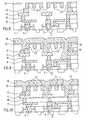
- FIGS. 1 - 8represent one embodiment of the present invention.
- FIG. 1represents a cross-sectional view of the substrate level of a CMOS chip structure after devices and isolations have been formed.
- FIG. 2represents the level shown in FIG. 1 after a first sacrificial dielectric layer has been deposited between the gates and planarized, and a first hard mask has been deposited overall.
- FIG. 3represents the structure shown in FIG. 2 after the hard mask has been selectively provided with openings and the sacrificial dielectric has been selectively etched and filled to form conductive vias. The remaining hard mask has been removed.
- FIG. 4represents the structure shown in FIG. 3 on which a second sacrificial dielectric layer has been deposited, selectively etched, and filled to form conductive vias at preselected locations.
- FIG. 5represents the structure shown in FIG. 4 on which a third sacrificial dielectric layer has been deposited, selectively etched, and filled to form a first local interconnect conductive wiring level in electrical communication with selected conductive vias that were formed in FIG. 4.
- FIG. 6represents the structure shown in FIG. 5 on which a final conductive via level, then a second wiring level have been formed in a sacrificial dielectric medium as described for preceding figures.
- a final hard maskhas been deposited overall and after formation of the second wiring level.
- FIGS. 1 - 9represent a second embodiment of the present invention
- CVD diamondhas been deposited as an encapsulant onto the FIG. 8 structure, sealing the lower interconnection levels from the external ambient.
- FIGS. 1 - 8 and 10represent a third embodiment of the present invention.
- CVD diamondhas only been removed from areas with high device, line or via packing density, limiting gas dielectric to those specific areas.
- CVD diamondis deposited as a temporary, sacrificial dielectric medium in the electrically interconnected levels of a CMOS IC chip structure.
- the CVD) diamondgives stability to the structure as it is being fabricated, but is no longer needed when the structure is completed. It is then removed from the entire structure by an isotropic oxygen etch through the openings in a nitride hard mask overlayer which have been defined by photolithography. The hard mask is left in place for stability.
- FIG. 1illustrates an example of the starting point of the present invention as applied to a CMOS BEOL chip.
- the substrate ( 0 ) materialcan be silicon, a silicon oxide, silicon/germanium, gallium arsenide or any such semiconductor.
- Oxide isolation regions ( 1 )are shown below substrate ( 0 ) and gates ( 2 ) are shown atop the substrate ( 0 ).
- metallizationsuch as wiring, and additional devices.
- CVD diamondthe temporary, sacrificial dielectric medium ( 3 )
- CVDchemical vapor deposition
- planarizedWhether or not planarization is necessary after deposition of CVD) diamond depends upon the demands of the integration scheme. Planarization can be performed by etch-back or CMP.
- a hard mask ( 4 )is deposited onto the planarized CVD diamond ( 3 ).
- the hard mask ( 4 )may be comprised of a silicon oxide, silicon nitride, or the like which can be deposited by sputtering or CVD. In this case the hard mask ( 4 ) is a nitride.
- vias ( 5 )have been filled with conductor, hard mask ( 4 ) is completely etched away and a second layer of sacrificial CVD diamond ( 6 ) is deposited and coated with a hard mask (not shown).
- the hard mask (not shown)is provided with openings using standard photolithographic techniques followed by oxygen etch through the openings and the underlying CVD diamond.
- the openingsare filled with conductor to make vias ( 7 ) connecting to selected gates and other vias and the remaining hard mask (not shown) is oxygen etched away.
- a second Damascene processcan be carried out using the same dielectric layer ( 6 ) to form local interconnect ( 8 ).
- a CVD diamond layer ( 9 )is deposited atop vias ( 7 ) and local interconnect ( 8 ), hard mask (not shown) is deposited followed by photolithography and oxygen etching of openings in the mask (not shown) and underlying CVD diamond (not shown), conductor is deposited to form vias ( 10 ), remaining etch mask (not shown) is removed and additional CVD diamond ( 16 ) is deposited.
- a hard mask (not shown)is subjected to photolithography, openings are oxygen etched through the openings and CVD diamond layer ( 16 ), and first wiring level ( 11 ) is deposited.
- second via level ( 12 )is fabricated, as is second wiring level ( 13 ).
- FIG. 6represents the final level.
- the final hard mask ( 15 )is not removed but is left to contribute to support of the structure when the sacrificial CVD) diamond dielectric is removed. In fact, hard mask ( 15 ) may provide sufficient support if there are not too many additional levels fabricated.
- additional alternating wiring and via levelscan be fabricated in the same manner as before, the number of levels depending on the requirements of the device on which the chip is to be mounted. In the interest of brevity, however, additional levels are not shown.
- photoresist ( 18 )is applied to final hard mask ( 15 ) and cure, openings ( 17 ) are exposed and developed in resist ( 16 ) and oxygen etched through hard mask ( 15 ). As shown in FIG. 8, the unexposed region of photoresist ( 18 ) is removed and openings ( 17 ) in mask ( 15 ) provide access for the removal of all sacrificial dielectric from the structure by isotropic oxygen etch.
- FIGS. 1 - 8 described above combined with FIG. 9represent a second embodiment of the present invention.
- a permanent cap of CVD diamond ( 19 )is deposited onto the chip as represented in FIG. 9.
- the CVD diamond of the cap ( 19 )is also deposited into the chip structure through the openings ( 17 ) in the hard mask ( 15 ), selectively sealing off lower interconnection levels from the ambient external to the chip. What is not shown is that by choice of layout the sides of the chip are also sealed. If the CVD diamond cap ( 19 ) is deposited in the atmosphere of an inert gas, such as argon or helium, that gas will be sealed within the chip rather than another.
- an inert gassuch as argon or helium
- a sealed structureprovides a more consistent dielectric medium by preventing the introduction of contaminants such as dirt of moisture from outside.
- the CVD diamond cap ( 19 )also provides improved thermal conductivity, a factor which becomes more important as the structure becomes more complex and increased heat is generated during use. Openings ( 17 ) in hard mask ( 15 ) shown in FIG. 8 provide sufficient access to remove all CVD diamond from within the chip, but the deposition of cap ( 19 ) into the same openings ( 17 ) forms columns ( 20 ) which block openings ( 17 ) and whose vertical progression into the chip is limited by features ( 11 ).
- FIGS. 1 - 8 described above combined with FIG. 10represent a third embodiment of the present invention.
- FIGS. 1 - 8the steps represented in FIGS. 1 - 8 have been completed. Rather than removing all CVD diamond from horizontal levels in the structure as shown in FIG. 8, however, the diamond is incompletely etched out from the lower levels of the chip, leaving some remaining in regions of relatively lower pattern density.
- CVD diamond levels ( 9 ), ( 16 ) and CVD diamond located in second via level ( 12 )are shown to be incompletely etched out.
- a partial removalprovides improved mechanical stability and thermal conductivity, especially in structures having many levels, while maintaining the benefit of low dielectric air gaps in regions of relatively higher pattern density at the upper levels as shown in FIG. 10.
- the intentis to have diamond in those areas where more mechanical support to the structure is required and to have air dielectric in those areas where very low dielectric constant is required.
Landscapes
- Business, Economics & Management (AREA)
- Engineering & Computer Science (AREA)
- Human Resources & Organizations (AREA)
- Physics & Mathematics (AREA)
- Development Economics (AREA)
- Economics (AREA)
- General Physics & Mathematics (AREA)
- Strategic Management (AREA)
- Theoretical Computer Science (AREA)
- Entrepreneurship & Innovation (AREA)
- General Business, Economics & Management (AREA)
- Marketing (AREA)
- Finance (AREA)
- Educational Administration (AREA)
- Accounting & Taxation (AREA)
- Operations Research (AREA)
- Game Theory and Decision Science (AREA)
- Technology Law (AREA)
- Quality & Reliability (AREA)
- Tourism & Hospitality (AREA)
- Condensed Matter Physics & Semiconductors (AREA)
- Manufacturing & Machinery (AREA)
- Computer Hardware Design (AREA)
- Microelectronics & Electronic Packaging (AREA)
- Power Engineering (AREA)
- Internal Circuitry In Semiconductor Integrated Circuit Devices (AREA)
- Logic Circuits (AREA)
Abstract
Description
- 1. Field of the Invention[0001]
- This invention relates to high density integrated circuit (IC) devices. More particularly, this invention relates to very high density multilevel interconnect electronic structures, and processes of fabricating such structures, which are comprised of alternating via levels and wiring levels embedded in a gas dielectric medium, suitable for mounting on carriers such as multichip modules.[0002]
- 2. Background Art[0003]
- The continuing drive toward reduction in dimensions and increase in the number and density of components within IC chips is inspired by increasingly more aggressive requirements of memory and logic. Smaller chip features provide higher bit density, lower operating voltages, lower energy consumption and faster device speed. Increased also are problems associated advanced IC miniaturization and the attendant closer proximity of circuit features to one another, including risk of shorting, crosstalk and capacitative coupling, among others. The highly dense integrated circuits of the future will require even narrower and longer conductor lines, tighter pitch via interconnects and lower dielectric constant values for the insulating medium, especially in the wiring levels. The lower the dielectric constant of the insulating medium, the faster the circuit speed.[0004]
- As the design demands for the CMOS IC in particular become more aggressive, the need to reduce the dielectric constant of the insulating medium to a value closer to the ideal value of air, 1.0, becomes a necessity. Attempts have been described in the art to incorporate air into a solid dielectric matrix, as in the form of foam or microspheres. More recently, attention has turned to the possiblility of employing air alone or some other gas as the dielectric medium in at least one level.[0005]
- Copending application Ser. No. 09/133,537 to Jagannathan et al filed Aug. 13, 1998 and assigned to the same assignee as the present invention describes the incorporation of air as a dielectric medium. The application describes the use of a fluoride-containing organic solvent for removing silicon-containing temporary dielectric material. The removal of the silicon-containing dielectric material leaves air-filled gaps to function as a permanent dielectric medium.[0006]
- U.S. Pat. No. 5,789,559 issued Aug. 25, 1998 to Subhas Bothra and Liang Q. Qian describes the formation of air dielectric between metallization layers as a result of the removal of a temporary solid dielectric material by a liquid etchant, buffered hydrofluoric acid (BHF).[0007]
- An article on pages 575-585 of the IBM Journal of Research and Development, Volume 42, No. 5, September. 1998, “Electrochemical processes for advanced package fabrication”, coauthored by S. Krongelb, J. A. Toredlo and L. T. Romankiw includes a description of a multilevel interconnect IC in which polyimide functions as a temporary dielectric. The polyimide- was removed by ashing in an oxygen-containing plasma. The IC chip also includes copper wiring, which was plated.[0008]
- An article on pages 49-51 of the journal Electrochemical and Solid State Letters, published by the Electrochemical Society, Inc. 1(1), 1998, “Air Gaps for Electrical Interonnections”, coauthored by Paul L. Kohl, Qiang Zhao, Kaushal Patel, Douglas Schmidt, Sue Ann Bidstrup-Allen, Robert Shick and S. Jayaraman describes the removal of a sacrificial polymer by thermal decomposition within an encapsulated chip. The byproducts escape by diffusing through the encapsulant.[0009]
- In the Technology News column on page 38 of the March 1999 edition of the journal Semiconductor International, Editor-in-Chief Peter Singer describes Toshiba's use of carbon dioxide gas dielectric in the wiring levels of an IC. The carbon dioxide is formed when the layer of carbon, which has been sputtered, is heated at 450 degrees C. in an oxygen atmosphere, resulting in the diffusion of oxygen to the carbon, where they combine to form CO2.[0010]
- An article on pages 51, 52, 54, 57, and 58 of the February, 1999 issue of the journal Solid State Technology, “Air gaps lower k of interconnect dielectric”, coauthors Ben Shieh, Krishna Saraswat, Mike Deal and Jim McVittio describe results of their modelling of air dielectric in structures having a variety of aluminum conductor line dimensions. Their simulation predicts a 40%-50% reduction in capacitance due to the air dielectric.[0011]
- In the present invention, wet processing can be limited to photolithographic processes, such as resist removal, which are conventionally used successfully and without contaminating the IC structure. Rather than using aggressive solvents to remove a temporary, sacrificial dielectric material, an isotropic oxygen etch is used to remove the sacrificial dielectric material cleanly. Wheras electroplating can be used to deposit such metals as copper and gold for wiring and interconnect vias in the present invention, dry deposition is preferred because extra steps such as those involved in establishing a barrier to electromigration of the metal into silicon are not required and because some useful metals and alloys are not amenable to plating. A wide variety of dielectric gasses can be protectively incorporated into the IC chip of the present invention. High temperature decomposition techniques play no role, nor is it necessary to fabricate passivation layers, such as on the substrate level. The present invention uniquely uses diamond-like carbon or diamond, preferably deposited by CVD, rather than, for example, a polymer or a silicon oxide as the temporary, sacrificial dielectric layer material. Since CVD diamond is a stronger material than polyimide or other dielectric polymer, use of the CVD diamond in the present invention will facilitate planarizaton by chemical-mechanical polishing (CMP). CVD diamond has the further advantage superior ability to conduct heat away from the IC chip which it encloses, in particular when a limited amount of CVD diamond is permitted to remain within the fabricated structure.[0012]
- The present invention includes the removal of sacrificial CVD diamond in a gas etchant, leaving gas-filled gaps to function as the permanent dielectric medium in, for example, a CMOS IC, a procedure not described in the art. The process of the present invention avoids any attack on or contamination of the elements of the IC structure and obviates any need to protect the gate level substrate by passivation, allowing the gate level the benefit of the low dielectric gas medium and avoiding passivatio-n steps. Furthermore the present invention describes a means of encapsulating the gas dielectric and an encapsulated CMOS IC not found in the art. The encapsulant eliminates diffusion of moisture or impurities into the encapsulated structure and confines the gas within. Several different gases can be used as alternative permanent dielectric media. These and other advantages and distinctions will be more fully evident infra.[0013]
- It is therefore an object of the invention to provide a multilevel interconnect CMOS IC chip having a gas insulating medium whose dielectric constant approaches or equals the ideal value of air.[0014]
- It is a further object of the invention to employ a CVD diamond sacrificial dielectric in conjunction with removal of the sacrificial dielectric by an isotropic oxygen etch to produce a very low-k IC chip.[0015]
- It is a further object of the invention -to provide an encapsulated multilevel interconnect CMOS IC chip having a gas insulating medium which is protected from exchange of material with the external ambient and away from which heat is readily conducted.[0016]
- It is a further object in an alternative mode of the invention to permit CVD diamond to remain in selected uncritical areas of the chip in order to provide additional structural support and thermal conductivity.[0017]
- It is a further object in an alternate mode of the invention to provide strategically located support structure in the form of pillars or studs in the process of forming an encapsulated structure which can be sealed at a later step.[0018]
- These and other objects are achieved according to the present invention in which, except for standard photolithographic steps, dry processing steps produce a high density CMOS IC which includes a gaseous dielectric medium interlevel and intralevel. The fabrication of the IC involves first including diamond-like carbon (DLC), diamond or preferably CVD diamond as a sacrificial dielectric material. Upon completion of the chip, prior to the deposition of final encapsulant, the sacrificial dielectric is removed harmlessly and selectively through openings in a hard mask top coat using an isotropic oxygen etch. Without compromising the electrical or mechanical integrity of the chip structure, the removal of the temporary, sacrificial dielectric material leaves behind regions in the structure which are filled with a permanent, gas dielectric medium. The sacrificial dielectric medium is also referred to herein as semi-sacrificial, as it is not necessarily the case that all of it must or should be removed from a particular IC configuration.[0019]
- In an embodiment of the present invention, the high density CMOS IC is sealed off from the ambient by an encapsulant. The seal assures a stable gaseous dielectric environment comprising such gases as air, CO2, nitrogen, inert gasses such as argon, helium, or others, and mixtures thereof. The encapsulant may also be controllably deposited in selected dielectric regions within the structure for additional mechanical support, leaving the remaining dielectric regions occupied by the air or other gas.[0020]
- FIGS.[0021]1-8 represent one embodiment of the present invention.
- FIG. 1 represents a cross-sectional view of the substrate level of a CMOS chip structure after devices and isolations have been formed.[0022]
- FIG. 2 represents the level shown in FIG. 1 after a first sacrificial dielectric layer has been deposited between the gates and planarized, and a first hard mask has been deposited overall.[0023]
- FIG. 3 represents the structure shown in FIG. 2 after the hard mask has been selectively provided with openings and the sacrificial dielectric has been selectively etched and filled to form conductive vias. The remaining hard mask has been removed.[0024]
- FIG. 4 represents the structure shown in FIG. 3 on which a second sacrificial dielectric layer has been deposited, selectively etched, and filled to form conductive vias at preselected locations.[0025]
- FIG. 5 represents the structure shown in FIG. 4 on which a third sacrificial dielectric layer has been deposited, selectively etched, and filled to form a first local interconnect conductive wiring level in electrical communication with selected conductive vias that were formed in FIG. 4.[0026]
- FIG. 6 represents the structure shown in FIG. 5 on which a final conductive via level, then a second wiring level have been formed in a sacrificial dielectric medium as described for preceding figures. A final hard mask has been deposited overall and after formation of the second wiring level.[0027]
- In the FIG. 7 representation, photoresist has been applied onto the final hard mask and openings have been patterned.[0028]
- In the FIG. 8 re-presentation, all the sacrificial dielectric has been removed from the structure through the openings patterned in the final hard mask.[0029]
- FIGS.[0030]1-9 represent a second embodiment of the present invention,
- In the FIG. 9 representation, CVD diamond has been deposited as an encapsulant onto the FIG. 8 structure, sealing the lower interconnection levels from the external ambient.[0031]
- FIGS.[0032]1-8 and10 represent a third embodiment of the present invention.
- In the FIG. 10 representation, CVD diamond has only been removed from areas with high device, line or via packing density, limiting gas dielectric to those specific areas.[0033]
- In order to facilitate understanding of the present invention, reference is made to the following detailed description taken in conjunction with the drawings.[0034]
- In one exemplary embodiment of the present invention, CVD diamond is deposited as a temporary, sacrificial dielectric medium in the electrically interconnected levels of a CMOS IC chip structure. The CVD) diamond gives stability to the structure as it is being fabricated, but is no longer needed when the structure is completed. It is then removed from the entire structure by an isotropic oxygen etch through the openings in a nitride hard mask overlayer which have been defined by photolithography. The hard mask is left in place for stability.[0035]
- FIG. 1 illustrates an example of the starting point of the present invention as applied to a CMOS BEOL chip. The substrate ([0036]0) material can be silicon, a silicon oxide, silicon/germanium, gallium arsenide or any such semiconductor. Oxide isolation regions (1) are shown below substrate (0) and gates (2) are shown atop the substrate (0). Not shown but potentially also disposed atop substrate (0) are metallization, such as wiring, and additional devices.
- In FIG. 2, CVD diamond, the temporary, sacrificial dielectric medium ([0037]3), is deposited onto the FIG. 1 structure by chemical vapor deposition (CVD) and planarized. Whether or not planarization is necessary after deposition of CVD) diamond depends upon the demands of the integration scheme. Planarization can be performed by etch-back or CMP. A hard mask (4) is deposited onto the planarized CVD diamond (3). The hard mask (4) may be comprised of a silicon oxide, silicon nitride, or the like which can be deposited by sputtering or CVD. In this case the hard mask (4) is a nitride.
- In a step not shown, standard photolithography procedures have been followed to expose openings in the hard mask ([0038]4) which have been isotropically oxygen etched through the CVD diamond (3) in order to provide openings for the deposition of metal to form conductive studs, also called vias (5), shown in FIG. 3.
- As FIG. 4 shows, vias ([0039]5) have been filled with conductor, hard mask (4) is completely etched away and a second layer of sacrificial CVD diamond (6) is deposited and coated with a hard mask (not shown). The hard mask (not shown) is provided with openings using standard photolithographic techniques followed by oxygen etch through the openings and the underlying CVD diamond. The openings are filled with conductor to make vias (7) connecting to selected gates and other vias and the remaining hard mask (not shown) is oxygen etched away. A second Damascene process can be carried out using the same dielectric layer (6) to form local interconnect (8).
- Several steps not shown have occurred between the fabrication of the structure shown in FIG. 4 and that shown in FIG. 5. However, the procedures are substantially the same as those described in relation to FIGS.[0040]2-4 above: a CVD diamond layer (9) is deposited atop vias (7) and local interconnect (8), hard mask (not shown) is deposited followed by photolithography and oxygen etching of openings in the mask (not shown) and underlying CVD diamond (not shown), conductor is deposited to form vias (10), remaining etch mask (not shown) is removed and additional CVD diamond (16) is deposited. Again, a hard mask (not shown) is subjected to photolithography, openings are oxygen etched through the openings and CVD diamond layer (16), and first wiring level (11) is deposited.
- In like manner second via level ([0041]12) is fabricated, as is second wiring level (13). FIG. 6 represents the final level. The final hard mask (15) is not removed but is left to contribute to support of the structure when the sacrificial CVD) diamond dielectric is removed. In fact, hard mask (15) may provide sufficient support if there are not too many additional levels fabricated. At the completion of wiring level (13) and prior to the application of final hard mask (15) when the first and second via levels and the first and second wiring levels have been completed, additional alternating wiring and via levels can be fabricated in the same manner as before, the number of levels depending on the requirements of the device on which the chip is to be mounted. In the interest of brevity, however, additional levels are not shown.
- As shown in FIG. 7, photoresist ([0042]18) is applied to final hard mask (15) and cure, openings (17) are exposed and developed in resist (16) and oxygen etched through hard mask (15). As shown in FIG. 8, the unexposed region of photoresist (18) is removed and openings (17) in mask (15) provide access for the removal of all sacrificial dielectric from the structure by isotropic oxygen etch.
- FIGS.[0043]1-8 described above combined with FIG. 9 represent a second embodiment of the present invention. When steps1-8 are completed, A permanent cap of CVD diamond (19) is deposited onto the chip as represented in FIG. 9. The CVD diamond of the cap (19) is also deposited into the chip structure through the openings (17) in the hard mask (15), selectively sealing off lower interconnection levels from the ambient external to the chip. What is not shown is that by choice of layout the sides of the chip are also sealed. If the CVD diamond cap (19) is deposited in the atmosphere of an inert gas, such as argon or helium, that gas will be sealed within the chip rather than another. A sealed structure provides a more consistent dielectric medium by preventing the introduction of contaminants such as dirt of moisture from outside. The CVD diamond cap (19) also provides improved thermal conductivity, a factor which becomes more important as the structure becomes more complex and increased heat is generated during use. Openings (17) in hard mask (15) shown in FIG. 8 provide sufficient access to remove all CVD diamond from within the chip, but the deposition of cap (19) into the same openings (17) forms columns (20) which block openings (17) and whose vertical progression into the chip is limited by features (11).
- FIGS.[0044]1-8 described above combined with FIG. 10 represent a third embodiment of the present invention.
- In the third embodiment of the present invention the steps represented in FIGS.[0045]1-8 have been completed. Rather than removing all CVD diamond from horizontal levels in the structure as shown in FIG. 8, however, the diamond is incompletely etched out from the lower levels of the chip, leaving some remaining in regions of relatively lower pattern density. In FIG. 9, CVD diamond levels (9), (16) and CVD diamond located in second via level (12) are shown to be incompletely etched out. A partial removal provides improved mechanical stability and thermal conductivity, especially in structures having many levels, while maintaining the benefit of low dielectric air gaps in regions of relatively higher pattern density at the upper levels as shown in FIG. 10. The intent is to have diamond in those areas where more mechanical support to the structure is required and to have air dielectric in those areas where very low dielectric constant is required.
- Although most of the description of the present invention has been presented in terms of using diamond, particularly CVD diamond, or DLC as a sacrificial dielectric, the above examples are intended to be illustrative rather than exhaustive, and while the invention has been described in conjunction with three specific embodiments, additional embodiments, modifications and applications will be apparent now and in the future, to those skilled in the art.[0046]
Claims (28)
1. A multilevel interconnect integrated circuit chip structure comprising in at least one of the multilevels a gaseous dielectric medium confined within the chip by a dielectric encapsulant.
2. The chip structure recited in
claim 1
3. The chip structure recited in
claim 1
4. The chip structure recited in
claim 1
5. A multilevel interconnect integrated circuit chip structure, comprising:
a. a semiconductor substrate supporting a substrate level metallization layer defining at least one device and at least one substrate-level conductive via interconnect;
b. a first conductive via level in electrical communication with selected ones of the at least one substrate-level conductive via interconnect and the at least one device;
c. a local interconnect wiring level in electrical communication with selected vias in the first conductive via level;
d. a preselected number of additional alternating conductive via levels and wiring levels in electrical communication;
e. a permanent hard mask disposed atop the final preselected level; and
f. a gaseous dielectric medium within at least one of the levels.
6. The multilevel interconnect integrated circuit chip structure recited in
claim 5
7. The multilevel interconnect integrated circuit chip structure recited in
claim 5
8. The multilevel interconnect integrated circuit chip structure recited in
claim 5
9. The multilevel interconnect integrated chip structure recited in
claim 5
10. The multilevel interconnect integrated circuit chip structure recited in
claim 5
11. The multilevel interconnect integrated circuit chip structure recited in
claim 5
12. The multilevel interconnect integrated circuit chip structure recited in
claim 5
13. The multilevel interconnect integrated circuit chip structure recited in
claim 12
14. The multilevel interconnect integrated circuit chip structure recited in
claim 5
15. The multilevel interconnect integrated circuit chip structure recited in
claim 14
16. The multilevel interconnect integrated circuit chip structure recited in
claim 5
17. A process for providing a gaseous dielectric medium within a multilevel interconnect integrated circuit chip, comprising the steps of:
a. providing a multilevel interconnect integrated circuit chip including a semi-sacrificial dielectric medium, and a hard mask final layer including a plurality of openings at preselected sites; and
b. removing the semi-sacrificial dielectric medium through any of the plurality of openings in the hard mask final layer by dry etching in an isotropic oxygen-containing gas, a gaseous dielectric medium thereby replacing the semi-sacrificial dielectric medium.
18. The process recited in
claim 17
19. The process recited in
claim 17
20. A process for making an integrated circuit chip having a gas dielectric medium, comprising the steps of:
a. providing a semiconductor substrate supporting a substrate-level metallization level defining at least one device and at least one substrate level conductive via interconnect;
b. depositing a first sacrificial CVD diamond layer to fill the substrate-level metallization level planar with the at least one device and at least one substrate level interconnect, and fabricating a first temporary hard mask onto the first sacrificial CVD diamond layer;
c. etching a preselected number of openings at preselected locations through the first, temporary hard mask and the first sacrificial CVD diamond layer, filling the openings with a conductive material to provide a first via level in electrical communication with the substrate metallization level, and removing the remaining first temporary hard mask;
d. depositing a second sacrificial CVD diamond layer onto the first sacrificial CVD diamond layer and fabricating a second temporary hard mask onto the second sacrificial CVD diamond layer;
e. etching a preselected number of openings at preselected locations through the second temporary hard mask and the second sacrificial CVD diamond layer, filling the openings with a conductive material to provide a local interconnect level in electrical communication with the first via level, and removing the second temporary hard mask;
f. repeating steps b through e until the desired number of levels is fabricated and a final, permanent hard mask is fabricated; and
g. etching a preselected number of openings at preselected locations in the final hard mask and removing at least some of the sacrificial CVD diamond dielectric terethrough, leaving a gas dielectric medium in the place of the removed sacrificial CVD diamond.
21. The process recited in
claim 20
22. The process recited in
claim 20
23. The process recited in
claim 20
24. The process recited in
claim 20
25. The process recited in
claim 20
26. The process recited in
claim 20
27. The process recited in
claim 20
28. A process for providing a gas dielectric medium in at least one level of a multilevel interconnect integrated circuit chip structure, which includes providing a diamond or diamond-like carbon dielectric material in the at least one level and, after completion of a preselected number of the multilevels, removing the dielectric material by etching in an isotropic oxygen etch through at least one opening in a final hard mask layer and encapsulating the chip structure.
Priority Applications (1)
| Application Number | Priority Date | Filing Date | Title |
|---|---|---|---|
| US09/825,653US6495445B2 (en) | 1999-07-02 | 2001-04-04 | Semi-sacrificial diamond for air dielectric formation |
Applications Claiming Priority (2)
| Application Number | Priority Date | Filing Date | Title |
|---|---|---|---|
| US09/347,839US6556962B1 (en) | 1999-07-02 | 1999-07-02 | Method for reducing network costs and its application to domino circuits |
| US09/825,653US6495445B2 (en) | 1999-07-02 | 2001-04-04 | Semi-sacrificial diamond for air dielectric formation |
Related Parent Applications (1)
| Application Number | Title | Priority Date | Filing Date |
|---|---|---|---|
| US09/347,839DivisionUS6556962B1 (en) | 1999-07-02 | 1999-07-02 | Method for reducing network costs and its application to domino circuits |
Publications (2)
| Publication Number | Publication Date |
|---|---|
| US20010014526A1true US20010014526A1 (en) | 2001-08-16 |
| US6495445B2 US6495445B2 (en) | 2002-12-17 |
Family
ID=23365502
Family Applications (2)
| Application Number | Title | Priority Date | Filing Date |
|---|---|---|---|
| US09/347,839Expired - Fee RelatedUS6556962B1 (en) | 1999-07-02 | 1999-07-02 | Method for reducing network costs and its application to domino circuits |
| US09/825,653Expired - Fee RelatedUS6495445B2 (en) | 1999-07-02 | 2001-04-04 | Semi-sacrificial diamond for air dielectric formation |
Family Applications Before (1)
| Application Number | Title | Priority Date | Filing Date |
|---|---|---|---|
| US09/347,839Expired - Fee RelatedUS6556962B1 (en) | 1999-07-02 | 1999-07-02 | Method for reducing network costs and its application to domino circuits |
Country Status (1)
| Country | Link |
|---|---|
| US (2) | US6556962B1 (en) |
Cited By (36)
| Publication number | Priority date | Publication date | Assignee | Title |
|---|---|---|---|---|
| US6413852B1 (en)* | 2000-08-31 | 2002-07-02 | International Business Machines Corporation | Method of forming multilevel interconnect structure containing air gaps including utilizing both sacrificial and placeholder material |
| US6555467B2 (en)* | 2001-09-28 | 2003-04-29 | Sharp Laboratories Of America, Inc. | Method of making air gaps copper interconnect |
| US20030186535A1 (en)* | 2002-03-26 | 2003-10-02 | Lawrence D. Wong | Method of making semiconductor device using a novel interconnect cladding layer |
| US6677209B2 (en) | 2000-02-14 | 2004-01-13 | Micron Technology, Inc. | Low dielectric constant STI with SOI devices |
| US6737723B2 (en) | 2000-02-14 | 2004-05-18 | Micron Technology, Inc. | Low dielectric constant shallow trench isolation |
| US20040253801A1 (en)* | 2003-06-13 | 2004-12-16 | Aptos Corporation | Ultimate low dielectric device and method of making the same |
| US20050026388A1 (en)* | 2002-07-18 | 2005-02-03 | Micron Technology, Inc. | Techniques to create low K ILD for BEOL |
| US20050040484A1 (en)* | 2002-10-22 | 2005-02-24 | Busta Heinz H. | MEM switching device and method for making same |
| US6875685B1 (en)* | 2003-10-24 | 2005-04-05 | International Business Machines Corporation | Method of forming gas dielectric with support structure |
| US6890847B1 (en) | 2000-02-22 | 2005-05-10 | Micron Technology, Inc. | Polynorbornene foam insulation for integrated circuits |
| US20050137882A1 (en)* | 2003-12-17 | 2005-06-23 | Cameron Don T. | Method for authenticating goods |
| WO2007113108A1 (en)* | 2006-03-30 | 2007-10-11 | Koninklijke Philips Electronics N.V. | Improving control of localized air gap formation in an interconnect stack |
| US7326980B2 (en) | 2002-08-28 | 2008-02-05 | Micron Technology, Inc. | Devices with HfSiON dielectric films which are Hf-O rich |
| US7335965B2 (en) | 1999-08-25 | 2008-02-26 | Micron Technology, Inc. | Packaging of electronic chips with air-bridge structures |
| US7388246B2 (en) | 2002-08-29 | 2008-06-17 | Micron Technology, Inc. | Lanthanide doped TiOx dielectric films |
| US20080166874A1 (en)* | 2007-01-05 | 2008-07-10 | International Business Machines Corporation | Formation of vertical devices by electroplating |
| US20080171431A1 (en)* | 2007-01-17 | 2008-07-17 | Chen-Hua Yu | Interconnects containing bilayer porous low-k dielectrics using different porogen to structure former ratio |
| US7402876B2 (en) | 2002-12-04 | 2008-07-22 | Micron Technology, Inc. | Zr— Sn—Ti—O films |
| US7405454B2 (en) | 2003-03-04 | 2008-07-29 | Micron Technology, Inc. | Electronic apparatus with deposited dielectric layers |
| US7410668B2 (en) | 2001-03-01 | 2008-08-12 | Micron Technology, Inc. | Methods, systems, and apparatus for uniform chemical-vapor depositions |
| US7422637B2 (en) | 2002-10-09 | 2008-09-09 | Applied Materials, Inc. | Processing chamber configured for uniform gas flow |
| US7560395B2 (en) | 2005-01-05 | 2009-07-14 | Micron Technology, Inc. | Atomic layer deposited hafnium tantalum oxide dielectrics |
| US7560793B2 (en) | 2002-05-02 | 2009-07-14 | Micron Technology, Inc. | Atomic layer deposition and conversion |
| US7572695B2 (en) | 2005-05-27 | 2009-08-11 | Micron Technology, Inc. | Hafnium titanium oxide films |
| US20090214169A1 (en)* | 2005-07-11 | 2009-08-27 | Linares Robert C | Structures formed in diamond |
| US7601649B2 (en) | 2004-08-02 | 2009-10-13 | Micron Technology, Inc. | Zirconium-doped tantalum oxide films |
| US7605030B2 (en) | 2006-08-31 | 2009-10-20 | Micron Technology, Inc. | Hafnium tantalum oxynitride high-k dielectric and metal gates |
| US7611959B2 (en) | 2002-12-04 | 2009-11-03 | Micron Technology, Inc. | Zr-Sn-Ti-O films |
| US7662729B2 (en) | 2005-04-28 | 2010-02-16 | Micron Technology, Inc. | Atomic layer deposition of a ruthenium layer to a lanthanide oxide dielectric layer |
| US7709402B2 (en) | 2006-02-16 | 2010-05-04 | Micron Technology, Inc. | Conductive layers for hafnium silicon oxynitride films |
| US20110054450A1 (en)* | 2005-01-11 | 2011-03-03 | Apollo Diamond, Inc | Diamond medical devices |
| US8501563B2 (en) | 2005-07-20 | 2013-08-06 | Micron Technology, Inc. | Devices with nanocrystals and methods of formation |
| CN103367364A (en)* | 2012-03-27 | 2013-10-23 | 中国科学院微电子研究所 | CMOS and method for fabricating the same |
| US20150200160A1 (en)* | 2010-02-18 | 2015-07-16 | Taiwan Semiconductor Manufacturing Company, Ltd. | Semiconductor structure having an air-gap region and a method of manufacturing the same |
| US10910416B2 (en)* | 2016-08-25 | 2021-02-02 | Sony Semiconductor Solutions Corporation | Semiconductor device, image pickup device, and method for manufacturing semiconductor device |
| US20220246662A1 (en)* | 2018-09-27 | 2022-08-04 | Sony Semiconductor Solutions Corporation | Semiconductor device, solid-state imaging device, and method of manufacturing semiconductor device |
Families Citing this family (29)
| Publication number | Priority date | Publication date | Assignee | Title |
|---|---|---|---|---|
| US6429120B1 (en) | 2000-01-18 | 2002-08-06 | Micron Technology, Inc. | Methods and apparatus for making integrated-circuit wiring from copper, silver, gold, and other metals |
| US7211496B1 (en)* | 1998-04-22 | 2007-05-01 | International Business Machines Corporation | Freestanding multiplayer IC wiring structure |
| US6709968B1 (en)* | 2000-08-16 | 2004-03-23 | Micron Technology, Inc. | Microelectronic device with package with conductive elements and associated method of manufacture |
| US6670719B2 (en) | 1999-08-25 | 2003-12-30 | Micron Technology, Inc. | Microelectronic device package filled with liquid or pressurized gas and associated method of manufacture |
| US6420262B1 (en) | 2000-01-18 | 2002-07-16 | Micron Technology, Inc. | Structures and methods to enhance copper metallization |
| US7262130B1 (en) | 2000-01-18 | 2007-08-28 | Micron Technology, Inc. | Methods for making integrated-circuit wiring from copper, silver, gold, and other metals |
| US6498364B1 (en)* | 2000-01-21 | 2002-12-24 | Agere Systems Inc. | Capacitor for integration with copper damascene processes |
| US6815329B2 (en)* | 2000-02-08 | 2004-11-09 | International Business Machines Corporation | Multilayer interconnect structure containing air gaps and method for making |
| US6423629B1 (en) | 2000-05-31 | 2002-07-23 | Kie Y. Ahn | Multilevel copper interconnects with low-k dielectrics and air gaps |
| US7363609B2 (en)* | 2001-07-26 | 2008-04-22 | International Business Machines Corporation | Method of logic circuit synthesis and design using a dynamic circuit library |
| EP1493183B1 (en)* | 2002-04-02 | 2012-12-05 | Dow Global Technologies LLC | Process for making air gap containing semiconducting devices and resulting semiconducting device |
| US6954912B2 (en)* | 2002-05-17 | 2005-10-11 | Fujitsu Limited | Error detection in dynamic logic circuits |
| JP3793143B2 (en)* | 2002-11-28 | 2006-07-05 | 株式会社シマノ | Bicycle electronic control device |
| US6930034B2 (en)* | 2002-12-27 | 2005-08-16 | International Business Machines Corporation | Robust ultra-low k interconnect structures using bridge-then-metallization fabrication sequence |
| US7107552B2 (en)* | 2003-06-10 | 2006-09-12 | Intel Corporation | Method and apparatus to analyze noise in a pulse logic digital circuit design |
| US7373615B2 (en)* | 2004-02-17 | 2008-05-13 | International Business Machines Corporation | Method for optimization of logic circuits for routability |
| US7005371B2 (en)* | 2004-04-29 | 2006-02-28 | International Business Machines Corporation | Method of forming suspended transmission line structures in back end of line processing |
| US7370301B2 (en)* | 2004-12-17 | 2008-05-06 | Stmicroelectronics, Inc. | Method and apparatus for mixing static logic with domino logic |
| US7331030B2 (en)* | 2004-12-17 | 2008-02-12 | Stmicroelectronics, Inc. | Method to unate a design for improved synthesizable domino logic flow |
| US8478669B1 (en)* | 2005-11-02 | 2013-07-02 | Verizon Services Corp. | Systems and methods for modeling telecommunication switch investments |
| US7649239B2 (en)* | 2006-05-04 | 2010-01-19 | Intel Corporation | Dielectric spacers for metal interconnects and method to form the same |
| FR2902910B1 (en)* | 2006-06-26 | 2008-10-10 | Coupling Wave Solutions Cws Sa | METHOD FOR MODELING NOISE INJECTED IN AN ELECTRONIC SYSTEM |
| US7772702B2 (en)* | 2006-09-21 | 2010-08-10 | Intel Corporation | Dielectric spacers for metal interconnects and method to form the same |
| US8250556B1 (en)* | 2007-02-07 | 2012-08-21 | Tilera Corporation | Distributing parallelism for parallel processing architectures |
| US20100140790A1 (en)* | 2008-12-05 | 2010-06-10 | Seagate Technology Llc | Chip having thermal vias and spreaders of cvd diamond |
| US8266569B2 (en)* | 2010-03-05 | 2012-09-11 | Advanced Micro Devices, Inc. | Identification of critical enables using MEA and WAA metrics |
| US9960110B2 (en) | 2011-12-30 | 2018-05-01 | Intel Corporation | Self-enclosed asymmetric interconnect structures |
| US8872349B2 (en) | 2012-09-11 | 2014-10-28 | Intel Corporation | Bridge interconnect with air gap in package assembly |
| US8772938B2 (en) | 2012-12-04 | 2014-07-08 | Intel Corporation | Semiconductor interconnect structures |
Family Cites Families (45)
| Publication number | Priority date | Publication date | Assignee | Title |
|---|---|---|---|---|
| JPS5939124A (en) | 1982-08-27 | 1984-03-03 | Toshiba Corp | CMOS logic circuit |
| JPS6119226A (en) | 1984-07-05 | 1986-01-28 | Hitachi Ltd | Level converting circuit |
| US5789559A (en) | 1988-06-17 | 1998-08-04 | Genelabs Technologies, Inc. | DNA sequences of enterically transmitted non-A/non-B hepatitis viral agent |
| US5121003A (en) | 1990-10-10 | 1992-06-09 | Hal Computer Systems, Inc. | Zero overhead self-timed iterative logic |
| JPH04239221A (en) | 1991-01-11 | 1992-08-27 | Nec Ic Microcomput Syst Ltd | Semiconductor integrated circuit |
| US5331568A (en)* | 1991-06-18 | 1994-07-19 | Microelectronics & Computer Technology Corporation | Apparatus and method for determining sequential hardware equivalence |
| CA2084443A1 (en)* | 1992-01-31 | 1993-08-01 | Leonard C. Swanson | Method of item selection for computerized adaptive tests |
| JPH0722583A (en) | 1992-12-15 | 1995-01-24 | Internatl Business Mach Corp <Ibm> | Multilayer circuit device |
| US5502646A (en)* | 1993-12-02 | 1996-03-26 | Nec Usa, Inc. | Selection of partial scan flip-flops to break feedback cycles |
| US5602753A (en)* | 1994-04-19 | 1997-02-11 | Matsushita Electric Industrial Co., Ltd. | Method and apparatus for estimating power dissipation and method and apparatus of determining layout/routing |
| US5668732A (en)* | 1994-06-03 | 1997-09-16 | Synopsys, Inc. | Method for estimating power consumption of a cyclic sequential electronic circuit |
| EP0717878A1 (en) | 1994-06-30 | 1996-06-26 | Koninklijke Philips Electronics N.V. | Display device |
| US5413962A (en) | 1994-07-15 | 1995-05-09 | United Microelectronics Corporation | Multi-level conductor process in VLSI fabrication utilizing an air bridge |
| US5488319A (en) | 1994-08-18 | 1996-01-30 | International Business Machines Corporation | Latch interface for self-reset logic |
| US5453708A (en) | 1995-01-04 | 1995-09-26 | Intel Corporation | Clocking scheme for latching of a domino output |
| JP3213198B2 (en)* | 1995-03-15 | 2001-10-02 | 株式会社東芝 | Power evaluation method for integrated circuits |
| US5661675A (en) | 1995-03-31 | 1997-08-26 | Intel Corporation | Positive feedback circuit for fast domino logic |
| US5568062A (en) | 1995-07-14 | 1996-10-22 | Kaplinsky; Cecil H. | Low noise tri-state output buffer |
| WO1997007471A1 (en)* | 1995-08-11 | 1997-02-27 | Hausman Robert E | Apparatus and method for modeling linear and quadratic programs |
| US5748012A (en) | 1995-12-06 | 1998-05-05 | International Business Machines Corporation | Methodology to test pulsed logic circuits in pseudo-static mode |
| US5731983A (en)* | 1995-12-29 | 1998-03-24 | Nec Usa, Inc. | Method for synthesizing a sequential circuit |
| US5825208A (en) | 1996-05-20 | 1998-10-20 | International Business Machines Corporation | Method and apparatus for fast evaluation of dynamic CMOS logic circuits |
| US5867036A (en) | 1996-05-29 | 1999-02-02 | Lsi Logic Corporation | Domino scan architecture and domino scan flip-flop for the testing of domino and hybrid CMOS circuits |
| US5886540A (en) | 1996-05-31 | 1999-03-23 | Hewlett-Packard Company | Evaluation phase expansion for dynamic logic circuits |
| US5831990A (en) | 1996-06-19 | 1998-11-03 | Hewlett-Packard Company | Test-mode control for dynamic logic gates |
| US5815005A (en) | 1996-07-19 | 1998-09-29 | Texas Instruments Incorporated | Power reduction circuits and systems for dynamic logic gates |
| US5796282A (en) | 1996-08-12 | 1998-08-18 | Intel Corporation | Latching mechanism for pulsed domino logic with inherent race margin and time borrowing |
| US5896399A (en) | 1996-12-11 | 1999-04-20 | International Business Machines Corporation | System and method for testing self-timed memory arrays |
| US5896046A (en) | 1997-01-27 | 1999-04-20 | International Business Machines Corporation | Latch structure for ripple domino logic |
| US5892372A (en) | 1997-01-27 | 1999-04-06 | International Business Machines Corporation | Creating inversions in ripple domino logic |
| US6052008A (en) | 1997-07-14 | 2000-04-18 | International Business Machines Corporation | Generation of true and complement signals in dynamic circuits |
| US6049231A (en) | 1997-07-21 | 2000-04-11 | Texas Instruments Incorporated | Dynamic multiplexer circuits, systems, and methods having three signal inversions from input to output |
| JP3036479B2 (en) | 1997-08-08 | 2000-04-24 | 日本電気株式会社 | Dynamic logic circuit |
| US6393409B2 (en)* | 1997-10-31 | 2002-05-21 | Morgan Stanley Dean Witter & Co. | Computer method and apparatus for optimizing portfolios of multiple participants |
| US6090153A (en)* | 1997-12-05 | 2000-07-18 | International Business Machines Corporation | Multi-threshold-voltage differential cascode voltage switch (DCVS) circuits |
| US6002272A (en) | 1997-12-23 | 1999-12-14 | Intel Corporation | Tri-rail domino circuit |
| US5942917A (en) | 1997-12-29 | 1999-08-24 | Intel Corporation | High speed ratioed CMOS logic structures for a pulsed input environment |
| US6104212A (en) | 1998-02-11 | 2000-08-15 | International Business Machines Corporation | Common domino circuit evaluation device |
| US6002292A (en) | 1998-03-13 | 1999-12-14 | International Business Machines Corporation | Method and apparatus to control noise in a dynamic circuit |
| US6016000A (en)* | 1998-04-22 | 2000-01-18 | Cvc, Inc. | Ultra high-speed chip semiconductor integrated circuit interconnect structure and fabrication method using free-space dielectrics |
| DE69933813T2 (en) | 1998-04-30 | 2007-04-12 | Texas Instruments Inc., Dallas | Hybrid precharge techniques for data and clock in dominological circuits that reduce the charge distribution during evaluation |
| US6087855A (en) | 1998-06-15 | 2000-07-11 | International Business Machines Corporation | High performance dynamic multiplexers without clocked NFET |
| US6133759A (en) | 1998-06-16 | 2000-10-17 | International Business Machines Corp. | Decoupled reset dynamic logic circuit |
| US6132969A (en)* | 1998-06-19 | 2000-10-17 | Rosetta Inpharmatics, Inc. | Methods for testing biological network models |
| US6204696B1 (en) | 1998-09-22 | 2001-03-20 | Intel Corporation | Domino circuits with high performance and high noise immunity |
- 1999
- 1999-07-02USUS09/347,839patent/US6556962B1/ennot_activeExpired - Fee Related
- 2001
- 2001-04-04USUS09/825,653patent/US6495445B2/ennot_activeExpired - Fee Related
Cited By (80)
| Publication number | Priority date | Publication date | Assignee | Title |
|---|---|---|---|---|
| US7335965B2 (en) | 1999-08-25 | 2008-02-26 | Micron Technology, Inc. | Packaging of electronic chips with air-bridge structures |
| US7387912B2 (en) | 1999-08-25 | 2008-06-17 | Micron Technology, Inc. | Packaging of electronic chips with air-bridge structures |
| US6770537B2 (en) | 2000-02-14 | 2004-08-03 | Micron Technology, Inc. | Low dielectric constant shallow trench isolation |
| US6780721B2 (en) | 2000-02-14 | 2004-08-24 | Micron Technology, Inc. | Low dielectric constant shallow trench isolation |
| US6677209B2 (en) | 2000-02-14 | 2004-01-13 | Micron Technology, Inc. | Low dielectric constant STI with SOI devices |
| US6737723B2 (en) | 2000-02-14 | 2004-05-18 | Micron Technology, Inc. | Low dielectric constant shallow trench isolation |
| US6756653B2 (en) | 2000-02-14 | 2004-06-29 | Micron Technology, Inc. | Low dielectric constant shallow trench isolation |
| US6953983B2 (en) | 2000-02-14 | 2005-10-11 | Micron Technology, Inc. | Low dielectric constant STI with SOI devices |
| US6890847B1 (en) | 2000-02-22 | 2005-05-10 | Micron Technology, Inc. | Polynorbornene foam insulation for integrated circuits |
| US6737725B2 (en) | 2000-08-31 | 2004-05-18 | International Business Machines Corporation | Multilevel interconnect structure containing air gaps and method for making |
| US6413852B1 (en)* | 2000-08-31 | 2002-07-02 | International Business Machines Corporation | Method of forming multilevel interconnect structure containing air gaps including utilizing both sacrificial and placeholder material |
| US20020127844A1 (en)* | 2000-08-31 | 2002-09-12 | International Business Machines Corporation | Multilevel interconnect structure containing air gaps and method for making |
| US7410668B2 (en) | 2001-03-01 | 2008-08-12 | Micron Technology, Inc. | Methods, systems, and apparatus for uniform chemical-vapor depositions |
| US6555467B2 (en)* | 2001-09-28 | 2003-04-29 | Sharp Laboratories Of America, Inc. | Method of making air gaps copper interconnect |
| US7214594B2 (en)* | 2002-03-26 | 2007-05-08 | Intel Corporation | Method of making semiconductor device using a novel interconnect cladding layer |
| US20030186535A1 (en)* | 2002-03-26 | 2003-10-02 | Lawrence D. Wong | Method of making semiconductor device using a novel interconnect cladding layer |
| US7589029B2 (en) | 2002-05-02 | 2009-09-15 | Micron Technology, Inc. | Atomic layer deposition and conversion |
| US7560793B2 (en) | 2002-05-02 | 2009-07-14 | Micron Technology, Inc. | Atomic layer deposition and conversion |
| US20050029609A1 (en)* | 2002-07-18 | 2005-02-10 | Micron Technology, Inc. | Techniques to create low K ILD for beol |
| US20060292858A1 (en)* | 2002-07-18 | 2006-12-28 | Micron Technology, Inc. | Techniques to create low K ILD for beol |
| US7157387B2 (en)* | 2002-07-18 | 2007-01-02 | Micron Technologies, Inc. | Techniques to create low K ILD for BEOL |
| US7190043B2 (en) | 2002-07-18 | 2007-03-13 | Micron Technology, Inc. | Techniques to create low K ILD for beol |
| US20050026388A1 (en)* | 2002-07-18 | 2005-02-03 | Micron Technology, Inc. | Techniques to create low K ILD for BEOL |
| US7326980B2 (en) | 2002-08-28 | 2008-02-05 | Micron Technology, Inc. | Devices with HfSiON dielectric films which are Hf-O rich |
| US7388246B2 (en) | 2002-08-29 | 2008-06-17 | Micron Technology, Inc. | Lanthanide doped TiOx dielectric films |
| US7422637B2 (en) | 2002-10-09 | 2008-09-09 | Applied Materials, Inc. | Processing chamber configured for uniform gas flow |
| US7317232B2 (en)* | 2002-10-22 | 2008-01-08 | Cabot Microelectronics Corporation | MEM switching device |
| US20050040484A1 (en)* | 2002-10-22 | 2005-02-24 | Busta Heinz H. | MEM switching device and method for making same |
| US7611959B2 (en) | 2002-12-04 | 2009-11-03 | Micron Technology, Inc. | Zr-Sn-Ti-O films |
| US7923381B2 (en) | 2002-12-04 | 2011-04-12 | Micron Technology, Inc. | Methods of forming electronic devices containing Zr-Sn-Ti-O films |
| US8445952B2 (en) | 2002-12-04 | 2013-05-21 | Micron Technology, Inc. | Zr-Sn-Ti-O films |
| US7402876B2 (en) | 2002-12-04 | 2008-07-22 | Micron Technology, Inc. | Zr— Sn—Ti—O films |
| US7410917B2 (en) | 2002-12-04 | 2008-08-12 | Micron Technology, Inc. | Atomic layer deposited Zr-Sn-Ti-O films using TiI4 |
| US7405454B2 (en) | 2003-03-04 | 2008-07-29 | Micron Technology, Inc. | Electronic apparatus with deposited dielectric layers |
| US6913946B2 (en)* | 2003-06-13 | 2005-07-05 | Aptos Corporation | Method of making an ultimate low dielectric device |
| US20040253801A1 (en)* | 2003-06-13 | 2004-12-16 | Aptos Corporation | Ultimate low dielectric device and method of making the same |
| US6875685B1 (en)* | 2003-10-24 | 2005-04-05 | International Business Machines Corporation | Method of forming gas dielectric with support structure |
| US20050087875A1 (en)* | 2003-10-24 | 2005-04-28 | International Business Machines Corporation | Method of forming gas dielectric with support structure |
| US20050137882A1 (en)* | 2003-12-17 | 2005-06-23 | Cameron Don T. | Method for authenticating goods |
| US7601649B2 (en) | 2004-08-02 | 2009-10-13 | Micron Technology, Inc. | Zirconium-doped tantalum oxide films |
| US8288809B2 (en) | 2004-08-02 | 2012-10-16 | Micron Technology, Inc. | Zirconium-doped tantalum oxide films |
| US7727905B2 (en) | 2004-08-02 | 2010-06-01 | Micron Technology, Inc. | Zirconium-doped tantalum oxide films |
| US8765616B2 (en) | 2004-08-02 | 2014-07-01 | Micron Technology, Inc. | Zirconium-doped tantalum oxide films |
| US7776762B2 (en) | 2004-08-02 | 2010-08-17 | Micron Technology, Inc. | Zirconium-doped tantalum oxide films |
| US8524618B2 (en) | 2005-01-05 | 2013-09-03 | Micron Technology, Inc. | Hafnium tantalum oxide dielectrics |
| US8278225B2 (en) | 2005-01-05 | 2012-10-02 | Micron Technology, Inc. | Hafnium tantalum oxide dielectrics |
| US7560395B2 (en) | 2005-01-05 | 2009-07-14 | Micron Technology, Inc. | Atomic layer deposited hafnium tantalum oxide dielectrics |
| US7602030B2 (en) | 2005-01-05 | 2009-10-13 | Micron Technology, Inc. | Hafnium tantalum oxide dielectrics |
| US20110054450A1 (en)* | 2005-01-11 | 2011-03-03 | Apollo Diamond, Inc | Diamond medical devices |
| US7662729B2 (en) | 2005-04-28 | 2010-02-16 | Micron Technology, Inc. | Atomic layer deposition of a ruthenium layer to a lanthanide oxide dielectric layer |
| US7572695B2 (en) | 2005-05-27 | 2009-08-11 | Micron Technology, Inc. | Hafnium titanium oxide films |
| US7700989B2 (en) | 2005-05-27 | 2010-04-20 | Micron Technology, Inc. | Hafnium titanium oxide films |
| US8058085B2 (en) | 2005-07-11 | 2011-11-15 | Apollo Diamond, Inc | Method of forming a waveguide in diamond |
| US8455278B2 (en) | 2005-07-11 | 2013-06-04 | Apollo Diamond, Inc | Method of forming a waveguide in diamond |
| US20090214169A1 (en)* | 2005-07-11 | 2009-08-27 | Linares Robert C | Structures formed in diamond |
| US8921914B2 (en) | 2005-07-20 | 2014-12-30 | Micron Technology, Inc. | Devices with nanocrystals and methods of formation |
| US8501563B2 (en) | 2005-07-20 | 2013-08-06 | Micron Technology, Inc. | Devices with nanocrystals and methods of formation |
| US8067794B2 (en) | 2006-02-16 | 2011-11-29 | Micron Technology, Inc. | Conductive layers for hafnium silicon oxynitride films |
| US7709402B2 (en) | 2006-02-16 | 2010-05-04 | Micron Technology, Inc. | Conductive layers for hafnium silicon oxynitride films |
| US8785312B2 (en) | 2006-02-16 | 2014-07-22 | Micron Technology, Inc. | Conductive layers for hafnium silicon oxynitride |
| US8097949B2 (en)* | 2006-03-30 | 2012-01-17 | Nxp B.V. | Control of localized air gap formation in an interconnect stack |
| US20090243108A1 (en)* | 2006-03-30 | 2009-10-01 | Laurent Gosset | Control of localized air gap formation in an interconnect stack |
| WO2007113108A1 (en)* | 2006-03-30 | 2007-10-11 | Koninklijke Philips Electronics N.V. | Improving control of localized air gap formation in an interconnect stack |
| US8084370B2 (en) | 2006-08-31 | 2011-12-27 | Micron Technology, Inc. | Hafnium tantalum oxynitride dielectric |
| US7605030B2 (en) | 2006-08-31 | 2009-10-20 | Micron Technology, Inc. | Hafnium tantalum oxynitride high-k dielectric and metal gates |
| US8759170B2 (en) | 2006-08-31 | 2014-06-24 | Micron Technology, Inc. | Hafnium tantalum oxynitride dielectric |
| US8466016B2 (en) | 2006-08-31 | 2013-06-18 | Micron Technolgy, Inc. | Hafnium tantalum oxynitride dielectric |
| US20100041244A1 (en)* | 2006-08-31 | 2010-02-18 | Micron Technology, Inc. | Hafnium tantalum oxynitride dielectric |
| US20080166874A1 (en)* | 2007-01-05 | 2008-07-10 | International Business Machines Corporation | Formation of vertical devices by electroplating |
| US7608538B2 (en)* | 2007-01-05 | 2009-10-27 | International Business Machines Corporation | Formation of vertical devices by electroplating |
| US8247905B2 (en) | 2007-01-05 | 2012-08-21 | International Business Machines Corporation | Formation of vertical devices by electroplating |
| US20080171431A1 (en)* | 2007-01-17 | 2008-07-17 | Chen-Hua Yu | Interconnects containing bilayer porous low-k dielectrics using different porogen to structure former ratio |
| US7723226B2 (en)* | 2007-01-17 | 2010-05-25 | Taiwan Semiconductor Manufacturing Company, Ltd. | Interconnects containing bilayer porous low-k dielectrics using different porogen to structure former ratio |
| US20150200160A1 (en)* | 2010-02-18 | 2015-07-16 | Taiwan Semiconductor Manufacturing Company, Ltd. | Semiconductor structure having an air-gap region and a method of manufacturing the same |
| US10361152B2 (en)* | 2010-02-18 | 2019-07-23 | Taiwan Semiconductor Manufacturing Company, Ltd. | Semiconductor structure having an air-gap region and a method of manufacturing the same |
| CN103367364A (en)* | 2012-03-27 | 2013-10-23 | 中国科学院微电子研究所 | CMOS and method for fabricating the same |
| US10910416B2 (en)* | 2016-08-25 | 2021-02-02 | Sony Semiconductor Solutions Corporation | Semiconductor device, image pickup device, and method for manufacturing semiconductor device |
| US20210118922A1 (en)* | 2016-08-25 | 2021-04-22 | Sony Semiconductor Solutions Corporation | Semiconductor device, image pickup device, and method for manufacturing semiconductor device |
| US11621283B2 (en)* | 2016-08-25 | 2023-04-04 | Sony Semiconductor Solutions Corporation | Semiconductor device, image pickup device, and method for manufacturing semiconductor device |
| US20220246662A1 (en)* | 2018-09-27 | 2022-08-04 | Sony Semiconductor Solutions Corporation | Semiconductor device, solid-state imaging device, and method of manufacturing semiconductor device |
Also Published As
| Publication number | Publication date |
|---|---|
| US6495445B2 (en) | 2002-12-17 |
| US6556962B1 (en) | 2003-04-29 |
Similar Documents
| Publication | Publication Date | Title |
|---|---|---|
| US6495445B2 (en) | Semi-sacrificial diamond for air dielectric formation | |
| US6255712B1 (en) | Semi-sacrificial diamond for air dielectric formation | |
| US11152298B2 (en) | Metal via structure | |
| US6140238A (en) | Self-aligned copper interconnect structure and method of manufacturing same | |
| US6984577B1 (en) | Damascene interconnect structure and fabrication method having air gaps between metal lines and metal layers | |
| US6184121B1 (en) | Chip interconnect wiring structure with low dielectric constant insulator and methods for fabricating the same | |
| US6605545B2 (en) | Method for forming hybrid low-K film stack to avoid thermal stress effect | |
| US6197681B1 (en) | Forming copper interconnects in dielectric materials with low constant dielectrics | |
| EP0346423A1 (en) | Improved planarization process | |
| JP2006352124A (en) | Semiconductor device and method for manufacturing the same | |
| US6806551B2 (en) | Fuse construction for integrated circuit structure having low dielectric constant dielectric material | |
| US6348734B1 (en) | Self-aligned copper interconnect architecture with enhanced copper diffusion barrier | |
| US6667552B1 (en) | Low dielectric metal silicide lined interconnection system | |
| US7592220B2 (en) | Capacitance process using passivation film scheme | |
| US6870263B1 (en) | Device interconnection | |
| US6191031B1 (en) | Process for producing multi-layer wiring structure | |
| US20070275565A1 (en) | Full removal of dual damascene metal level | |
| US6218282B1 (en) | Method of forming low dielectric tungsten lined interconnection system | |
| US11101175B2 (en) | Tall trenches for via chamferless and self forming barrier | |
| US5880030A (en) | Unlanded via structure and method for making same | |
| US10763160B1 (en) | Semiconductor device with selective insulator for improved capacitance | |
| US6524944B1 (en) | Low k ILD process by removable ILD | |
| US7060193B2 (en) | Method to form both high and low-k materials over the same dielectric region, and their application in mixed mode circuits | |
| US7015589B2 (en) | Semiconductor device having low-k dielectric film in pad region | |
| US6465343B1 (en) | Method for forming backend interconnect with copper etching and ultra low-k dielectric materials |
Legal Events
| Date | Code | Title | Description |
|---|---|---|---|
| FEPP | Fee payment procedure | Free format text:PAYOR NUMBER ASSIGNED (ORIGINAL EVENT CODE: ASPN); ENTITY STATUS OF PATENT OWNER: LARGE ENTITY | |
| FPAY | Fee payment | Year of fee payment:4 | |
| REMI | Maintenance fee reminder mailed | ||
| LAPS | Lapse for failure to pay maintenance fees | ||
| STCH | Information on status: patent discontinuation | Free format text:PATENT EXPIRED DUE TO NONPAYMENT OF MAINTENANCE FEES UNDER 37 CFR 1.362 | |
| FP | Lapsed due to failure to pay maintenance fee | Effective date:20101217 |