US20010014371A1 - Apparatus for growing thin films - Google Patents
Apparatus for growing thin filmsDownload PDFInfo
- Publication number
- US20010014371A1 US20010014371A1US09/749,339US74933900AUS2001014371A1US 20010014371 A1US20010014371 A1US 20010014371A1US 74933900 AUS74933900 AUS 74933900AUS 2001014371 A1US2001014371 A1US 2001014371A1
- Authority
- US
- United States
- Prior art keywords
- substrate
- reactants
- reaction space
- reaction
- inlet
- Prior art date
- Legal status (The legal status is an assumption and is not a legal conclusion. Google has not performed a legal analysis and makes no representation as to the accuracy of the status listed.)
- Granted
Links
Images


Classifications
- H—ELECTRICITY
- H01—ELECTRIC ELEMENTS
- H01L—SEMICONDUCTOR DEVICES NOT COVERED BY CLASS H10
- H01L21/00—Processes or apparatus adapted for the manufacture or treatment of semiconductor or solid state devices or of parts thereof
- H01L21/02—Manufacture or treatment of semiconductor devices or of parts thereof
- H01L21/04—Manufacture or treatment of semiconductor devices or of parts thereof the devices having potential barriers, e.g. a PN junction, depletion layer or carrier concentration layer
- H01L21/18—Manufacture or treatment of semiconductor devices or of parts thereof the devices having potential barriers, e.g. a PN junction, depletion layer or carrier concentration layer the devices having semiconductor bodies comprising elements of Group IV of the Periodic Table or AIIIBV compounds with or without impurities, e.g. doping materials
- H01L21/20—Deposition of semiconductor materials on a substrate, e.g. epitaxial growth solid phase epitaxy
- C—CHEMISTRY; METALLURGY
- C23—COATING METALLIC MATERIAL; COATING MATERIAL WITH METALLIC MATERIAL; CHEMICAL SURFACE TREATMENT; DIFFUSION TREATMENT OF METALLIC MATERIAL; COATING BY VACUUM EVAPORATION, BY SPUTTERING, BY ION IMPLANTATION OR BY CHEMICAL VAPOUR DEPOSITION, IN GENERAL; INHIBITING CORROSION OF METALLIC MATERIAL OR INCRUSTATION IN GENERAL
- C23C—COATING METALLIC MATERIAL; COATING MATERIAL WITH METALLIC MATERIAL; SURFACE TREATMENT OF METALLIC MATERIAL BY DIFFUSION INTO THE SURFACE, BY CHEMICAL CONVERSION OR SUBSTITUTION; COATING BY VACUUM EVAPORATION, BY SPUTTERING, BY ION IMPLANTATION OR BY CHEMICAL VAPOUR DEPOSITION, IN GENERAL
- C23C16/00—Chemical coating by decomposition of gaseous compounds, without leaving reaction products of surface material in the coating, i.e. chemical vapour deposition [CVD] processes
- C23C16/44—Chemical coating by decomposition of gaseous compounds, without leaving reaction products of surface material in the coating, i.e. chemical vapour deposition [CVD] processes characterised by the method of coating
- C23C16/455—Chemical coating by decomposition of gaseous compounds, without leaving reaction products of surface material in the coating, i.e. chemical vapour deposition [CVD] processes characterised by the method of coating characterised by the method used for introducing gases into reaction chamber or for modifying gas flows in reaction chamber
- C23C16/45523—Pulsed gas flow or change of composition over time
- C23C16/45525—Atomic layer deposition [ALD]
- C23C16/45544—Atomic layer deposition [ALD] characterized by the apparatus
- C23C16/45546—Atomic layer deposition [ALD] characterized by the apparatus specially adapted for a substrate stack in the ALD reactor
- C—CHEMISTRY; METALLURGY
- C30—CRYSTAL GROWTH
- C30B—SINGLE-CRYSTAL GROWTH; UNIDIRECTIONAL SOLIDIFICATION OF EUTECTIC MATERIAL OR UNIDIRECTIONAL DEMIXING OF EUTECTOID MATERIAL; REFINING BY ZONE-MELTING OF MATERIAL; PRODUCTION OF A HOMOGENEOUS POLYCRYSTALLINE MATERIAL WITH DEFINED STRUCTURE; SINGLE CRYSTALS OR HOMOGENEOUS POLYCRYSTALLINE MATERIAL WITH DEFINED STRUCTURE; AFTER-TREATMENT OF SINGLE CRYSTALS OR A HOMOGENEOUS POLYCRYSTALLINE MATERIAL WITH DEFINED STRUCTURE; APPARATUS THEREFOR
- C30B25/00—Single-crystal growth by chemical reaction of reactive gases, e.g. chemical vapour-deposition growth
- C30B25/02—Epitaxial-layer growth
- C30B25/14—Feed and outlet means for the gases; Modifying the flow of the reactive gases
- Y—GENERAL TAGGING OF NEW TECHNOLOGICAL DEVELOPMENTS; GENERAL TAGGING OF CROSS-SECTIONAL TECHNOLOGIES SPANNING OVER SEVERAL SECTIONS OF THE IPC; TECHNICAL SUBJECTS COVERED BY FORMER USPC CROSS-REFERENCE ART COLLECTIONS [XRACs] AND DIGESTS
- Y10—TECHNICAL SUBJECTS COVERED BY FORMER USPC
- Y10S—TECHNICAL SUBJECTS COVERED BY FORMER USPC CROSS-REFERENCE ART COLLECTIONS [XRACs] AND DIGESTS
- Y10S206/00—Special receptacle or package
- Y10S206/832—Semiconductor wafer boat
Definitions
- a preferred embodiment of the inventionhas the parallel reactant infeed channels of the sprayhead manifold adapted to open at least substantially perpendicular to the longitudinal axis of the substrates, whereby the number of substrates laced in the substrate holder box can be varied without changing the distance between the infeed channels.
Landscapes
- Chemical & Material Sciences (AREA)
- Engineering & Computer Science (AREA)
- General Chemical & Material Sciences (AREA)
- Chemical Kinetics & Catalysis (AREA)
- Materials Engineering (AREA)
- Metallurgy (AREA)
- Organic Chemistry (AREA)
- Mechanical Engineering (AREA)
- Crystallography & Structural Chemistry (AREA)
- Physics & Mathematics (AREA)
- Condensed Matter Physics & Semiconductors (AREA)
- General Physics & Mathematics (AREA)
- Manufacturing & Machinery (AREA)
- Computer Hardware Design (AREA)
- Microelectronics & Electronic Packaging (AREA)
- Power Engineering (AREA)
- Chemical Vapour Deposition (AREA)
Abstract
Description
- This application claims the priority benefit under 35 U.S.C. §119 to Finnish patent application Ser. No. 19992797, filed Dec. 28, 1999, the entire content of which is hereby expressly incorporated by reference.[0001]
- The present invention relates to an apparatus for growing thin films on a surface of a substrate. More particularly, the present invention relates to an apparatus for producing thin films on a surface of a substrate by subjecting the substrate to alternately repeated surface reactions of vapor-phase reactants.[0002]
- Conventionally, thin-films are grown using vacuum evaporation deposition, the Molecular Beam Epitaxy (MBE) and other similar vacuum deposition methods, different variants of the Chemical Vapor Deposition (CVD) method (including low-pressure and organometallic CVD and plasma-enhanced CVD) or a deposition method of alternately repeated surface reactions called the Atomic Layer Epitaxy (ALE) or Atomic Layer Deposition (ALD).[0003]
- In MBE and CVD methods, the thin film growth rate is determined by the concentrations of the provided starting material in addition to other process variables. To achieve a uniform thickness of the layers deposited by these methods, the concentrations and reactivities of starting materials must be carefully kept constant on different surface areas of the substrate. If the different starting materials are allowed to mix with each other prior to reaching the substrate surface, as is the case in the CVD method, for instance, a chance of their mutual reaction arises. Then, a risk of microparticle formation already within the infeed channels of the gaseous reactants is imminent. Such microparticles generally have a deteriorating effect on the quality of the deposited thin film. Therefore, the possibility of premature reactions in MBE and CVD reactors, for instance, is avoided by heating the starting materials not earlier than at the substrate surfaces. In addition to heating, the desired reaction can be initiated using, e.g., a plasma discharge or other similar activating means.[0004]
- In the MBE and CVD processes, the growth of thin films is primarily adjusted by controlling the infeed rates of starting materials impinging on the substrate. In contrast, the growth rate in the ALE process is controlled by the substrate surface qualities, rather than the starting material concentrations or flow variables. The only prerequisite in the ALE process is that the starting material is available in sufficient concentration to saturate the surface of the substrate. The ALE method is described, for example, in FI patent publications 52,359 and 57,975 and in U.S. patent publications 4,058,430 and 4,389,973. Equipment constructions suited to implement this method are disclosed in patent publications U.S. 5,855,680 and FI 100,409. Apparatuses for growing thin films are also described in the following publications: Material Science Report 4(7) (1989), p. 261, and Tyhjiötekniikka (Finnish publication for vacuum techniques), ISBN 951-794-422-5, pp. 253-261. These references are incorporated herein by reference.[0005]
- In the ALE growth method described in FI Pat. No. 57,975, the reactant atoms or molecules are arranged to sweep over the substrates, thus impinging on their surface until a fully saturated molecular layer is formed thereon. Next, the excess reactant and the gaseous reaction products are removed from the substrates with the help of inert gas pulses passed over the substrates or, alternatively, by pumping the reaction space to a vacuum before the next gaseous pulse of a different reactant is admitted. The succession of the different gaseous reactant pulses and the diffusion barriers formed by the separating inert gas pulses or cycles of vacuum pumping result in a thin film growth controlled by the individual surface-chemical reactions of all these components. If necessary, the effect of the vacuum pumping cycle may be augmented by the inert gas flow. For the function of the process, it is typically irrelevant whether the gaseous reactants or the substrates are kept in motion; it only matters to keep the different reactants of the successive reactions separate from each other and to have them sweep successively over the substrate.[0006]
- Most vacuum evaporators operate on the so-called “single-shot” principle. Hereby, a vaporized atom or molecule can impinge on the substrate only once. If no reaction with the substrate surface occurs, the atom/molecule is rebound or revaporized so as to hit the apparatus walls or the vacuum pump, undergoing condensation therein. In hot-walled reactors, an atom or molecule that collides with the process chamber wall or the substrate can undergo revaporization and, hence, repeated impingements on the substrate. When applied to ALE process chambers, this “multi-shot” principle can offer a number of benefits including improved efficiency of material consumption.[0007]
- ALE reactions operating on the “multi-shot” principle generally are designed for the use of a cassette unit in which a plurality of substrates can be taken simultaneously into the process chamber or, alternatively, the substrates can be placed unmountedly into the process space formed by a pressure vessel, whereby the process space also serves as the reaction chamber wherein the vapor-phase reactants are reacted with the substrate surface in order to grow thin film structures. If a cassette unit designed for holding several substrates is employed, the reaction chamber is formed in the interior of the cassette unit. Use of a cassette unit shortens the growth time per substrate in respect to single-substrate cycling, whereby a higher production throughput is attained. Furthermore, a cassette unit arranged to be movable into and out from the process chamber can be dismantled and cleaned without interrupting the production flow because one cassette unit can be used in the process chamber while another one is being cleaned.[0008]
- Batch processing is preferred in conventional ALE thin film processes because of the relatively slow production pace of the ALE method relative to other thin film growth techniques. The overall growth time per substrate of a thin film structure can be reduced in a batch process to a more competitive level. For the same reason, larger substrate sizes are also preferred.[0009]
- In one embodiment of the ALE technique, the framework of the cassette unit is formed by a holder box made from titanium, for instance, having a structure with open top and bottom ends, whereby the holder box can support a plurality of substrates inserted therein into a longitudinally parallel position. The substrates have their ends or perimeters mounted in frames that are further placed into grooves formed at opposite ends of the substrate holder box. Each substrate frame has two substrates mounted therein with the back sides of the substrates facing each other. Herein, the back side of a substrate refers to that face of the substrate on which no thin film is to be grown. The access of reactants into any space that remains between the back sides of the substrates is prevented by covering the longitudinal top and bottom edges of the substrates with protecting continuous seal sections. The reactants and the inert gas are passed into the holder box via the infeed holes of the parallel infeed channels of a sprayhead manifold located above the holder box. Of course, the sprayhead construction may be varied as required. The excess reactants and reaction gases are removed from the holder box via discharge channels of a suction box connected to, at the bottom part of the holder box. In this manner, the gases are forced to flow through the spaces remaining between the faces of the substrates on which a thin film is to be grown.[0010]
- Feeding the gaseous reactants into the holder box from one end only may cause stronger film growth on substrate surface areas located closer to the infeed of reactants. In order to compensate for this effect, the gases can be fed onto the substrates alternately from opposite directions. In such an arrangement, the exhaust suction through the outfeed channel are typically arranged to also take place alternately at opposite ends. Due to the alternating infeed cycles, infeed/discharge nozzles must be located at both the top and bottom ends of the holder box, which complicates the construction substantially.[0011]
- It is therefore an object of the present invention to provide a novel type of ALE reaction chamber featuring improved reactant flow conditions over those known in the art, whereby a smooth thin film growth is obtained on the substrate surface.[0012]
- Accordingly, one aspect of the invention involves placing the substrates in a substrate holder box of a cassette unit longitudinally side-by-side in an A-shape inclined disposition with their back sides facing each other so that the distance between the opposed surfaces, which are intended to support the thin film growth and between which the gases are arranged to flow, is narrower at the gas infeed end than at the gas outfeed end. In other words, the A-shape inclined disposition of the opposed surfaces being deposited with a thin film opens in the flow direction of reactant gases, whereby the cross section of the gas flow channel becomes larger in the flow direction and, as a result, the flow speed decreases toward the outfeed end of the substrate holder box. Furthermore, a preferred embodiment of the invention has the parallel reactant infeed channels of the sprayhead manifold adapted to open at least substantially perpendicular to the longitudinal axis of the substrates, whereby the number of substrates laced in the substrate holder box can be varied without changing the distance between the infeed channels.[0013]
- More specifically, the invention relates to an apparatus that comprises a reaction chamber including a reaction space, infeed means connected to the reaction space for feeding into the reaction space the reactants used in the thin film growth process, and outfeed means connected to the reaction space for discharging excess reactants and gaseous reaction products from the reaction space. At least one substrate is provided within the reaction space and a second surface is opposed to the surface of the substrate on which the thin film is to be grown. The reactants are forced to flow in relation to the opposed surfaces in the space formed therebetween. The thin-film growth supporting surface of the substrate and the surface disposed opposing the same are arranged into the reaction chamber so as to subtend an angle opening in the flow direction of the reactants in relation to the opposed surfaces, whereby the distance between the opposed surfaces and the infeed end of reactants is smaller than at the gas outfeed end.[0014]
- The invention offers significant benefits. For example, by placing the substrates in an A-shape inclined disposition opening in the flow direction of the reactants and the reaction gases, the thin film grown on the substrate surfaces becomes more uniform than what is obtained through a constant spacing between the substrates and more uniform than what is obtained by locating the substrate surfaces intended to support the thin film growth into an A-shape opposed disposition so that the gas flow is restricted as it flows toward the closing apex.[0015]
- If the sprayhead serving for the infeed of reactants and inert gases is located at the top of the cassette unit, a pair of substrates with their back sides opposing each other will be disposed in a single substrate frame so as to form an inverted letter A. When the substrate frames are then placed in the holder box, they will fit tightly by their own weight against the upward walls in the V-shape aligned grooves made in the ends of the substrate holder box. The accurate placement of the substrates prevents any gas flow from escaping to the back sides of the substrates.[0016]
- To avoid intermixing of reactants, it is preferable to keep the infeed channels of the different reactants separate from each other as long as possible. In prior-art constructions, the infeed channels of reactants and inert gas have been arranged to open into the cassette unit in the direction of the longitudinal axes of the substrates, whereby any change in the batch of substrates to be processed has also required changes in the distance or number of infeed channels in order to provide gas flow into all the spaces between the substrate surfaces on which a thin film is to be grown. In the preferred embodiment of the invention, the infeed channels of the sprayheads are located at right angles to the longitudinal axes of the substrates, whereby the number of substrates placed in the cassette unit can be varied without altering the distance between the infeed channels or the number thereof.[0017]
- It should be noted that certain objects and advantages of the invention have been described above for the purpose of describing the invention and the advantages achieved over the prior art. Of course, it is to be understood that not necessarily all such objects or advantages may be achieved in accordance with any particular embodiment of the invention. Thus, for example, those skilled in the art will recognize that the invention may be embodied or carried out in a manner that achieves or optimizes one advantage or group of advantages as taught herein without necessarily achieving other objects or advantages as may be taught or suggested herein.[0018]
- It should also be noted that all of these embodiments are intended to be within the scope of the invention herein disclosed. These and other embodiments of the present invention will become readily apparent to those skilled in the art from the following detailed description of the preferred embodiments having reference to the attached figures, the invention not being limited to any particular preferred embodiment(s) disclosed.[0019]
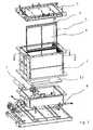
- In the following, the invention will be described in greater detail with the help of exemplifying embodiments illustrated in the appended drawings, in which[0020]
- FIG. 1 is an exploded view of an apparatus for growing thin films onto the surface of a substrate having certain features and advantages according to the present invention;[0021]
- FIG. 2 is a more detailed view of a substrate holder box of the apparatus depicted in FIG. 1; and[0022]
- FIG. 3 is a schematic cross-sectional layout view of substrates placed in parallel frames.[0023]
- In the context of the present invention, the term “reactant” refers to a gas or a vaporizable solid or liquid starting material capable of reacting with the surface of the substrate. The ALE method conventionally uses reactants selected from two separate groups. The term “metallic reactants” is used of metallic compounds which may even be elemental metals. Suitable metallic reactants are the halogenides of metals including chlorides and bromides, for instance, and organometallic compounds such as the thd complex compounds. The following are examples of metallic reactants that can used Zn, ZnCl[0024]2, Ca(thd)2, (CH3)3Al and Cp2Mg. The term “nonmetallic reactants” is used for compounds and elements capable of reacting with metallic compounds. The latter group is appropriately represented by water, sulfur, hydrogen sulfide and ammonia.
- In the present context, the term “protective gas” is used when reference is made to a gas which is admitted into the reaction space and is capable of preventing undesired reactions related to the reactants and, correspondingly, the substrate. Such reactions include, for example, the reactions of reactants and the substrate with possible impurities. The protective gas also serves to prevent reactions between substances of different reactant groups in, for example, the infeed piping. In the method according to the invention, the protective gas is also preferably used as the carrier gas of the vapor-phase pulses of the reactants. According to a preferred embodiment, in which reactants of different reactant groups are admitted via separate infeed manifolds into the reaction space, the vapor-phase reactant pulse is admitted from one infeed channel while the protective gas is admitted from another infeed channel thus preventing admitted reactants from entering the reactant infeed channel of another reactant group. Examples of suitable protective gases are inert gases such as nitrogen and noble gases, for example, argon. The protective gas may also be an inherently reactive gas such as hydrogen gas selected to prevent undesirable reactions (e.g., oxidization reactions) from occurring on the substrate surface.[0025]
- According to the invention, the term “reaction chamber” includes both the reaction space in which the substrate is located and in which the vapor-phase reactants are allowed to react with the substrate in order to grow thin films, as well as the gas infeed/outfeed channels communicating immediately with the reaction space. These channels serve to admit the reactants into the reaction space (infeed channels) or to remove the gaseous reaction products and excess reactants of the thin-film growth process from the reaction space (outfeed channels). A substrate located in this kind of reaction chamber is subjected to alternately repeated surface reactions of at least two different reactants used for producing a thin film. The vapor-phase reactants are preferably admitted repetitively and alternatingly, with each reactant preferably being fed separately from its own source into the reaction chamber, where they are allowed to react with the substrate surface for the purpose of forming a solid-state thin film product on the substrate. Reaction products that have not adhered onto the substrate, and any possible excess reactant, are removed from the reaction chamber in the vapor phase.[0026]
- Herein, the term “substrate surface” is used to denote that surface of the substrate onto which the vapor-phase reactant flowing into the reaction chamber impinges. In practice, the surface, during the first cycle of the thin-film growing process is constituted by the surface of a substrate such as glass or semi conductor wafer, for instance, or some other starting surface. During the second cycle, the surface is constituted by the layer formed during the first cycle and comprising the solid-state reaction product which is deposited by the reaction between the reactants and is adhered to the substrate, etc.[0027]
- The term “process chamber” is used when reference is made to the space in which the thin film growth process is carried out and which is preferably isolated from its environment in a tightly sealable manner. The reaction chamber is located in the process chamber and, further, a single process chamber may incorporate a plurality of reaction chambers.[0028]
- FIGS.[0029]1-3 illustrate an ALE apparatus for growing thin films onto the surface of a substrate having certain features and aspects according to the present invention. FIGS. 1 and 2 illustrate a portion of the process chamber including the reaction chamber, which includes a
cassette unit 1 acting as the reaction space and asprayhead 2. Thesprayhead 2 includes the reactant and the protective gas infeed channels and is attachable to the top of reaction chamber. Preferably, thecassette unit 1 is made from titanium and preferably incorporates at its both inner ends fastening means such asgrooves 3. Asupport flame element 5 is preferably adapted between each pair ofsubstrates 4, to both ends thereof. Preferably, on eachsupport frame element 5 are mounted twosubstrates 4 with their back sides facing each other. Here, the term substrate back side refers to that face of thesubstrate 4 on which no thin film is to be grown. The back sides of theopposed substrates 4 may be abutting each other, spaced apart from each other by a gap or, in a modified arrangement, a temperature equalizing or actively heated spacer plate may be inserted between them. The top and bottom edges ofsubstrates 4 placed in the samesupport frame element 5 are preferably covered by acontinuous seal section 6 serving to inhibit gases from reaching into any space remaining between the back sides of theopposed substrates 4. Thesubstrates 4 mounted with their back sides opposed to each other in thesupport frame element 5 are placed ingrooves 3 made in thecassette unit 1. - The entity formed by the[0030]
sprayhead 2, thecassette unit 1 with thesubstrates 4, thesupport frame elements 5 and thecontinuous seal sections 6 can be moved as such outside the process chamber. Thecassette unit 1 is preferably mounted into the process chamber on a preferably permanently fixedsuction box 8 that incorporatesgas outfeed channels 7, whereby thecassette unit 1, thesprayhead 2 and thesuction box 8 form the reaction chamber of the ALE apparatus. The reactants and the inert gas are passed into the reaction chamber via the parallel manifold channels of thesprayhead 2. Of course, other constructions of thesprayhead 2 can be used. The gas flow travels toward thesuction box 8 along the flow channels formed by opposed substrate surfaces (“front side”)on which the thin film is being deposited. The gas flow exits the reaction chamber via theoutfeed channels 7 of thesuction box 8. To augment the gas flow, a funnel-likegas flow guide 12 can be mounted between thecassette unit 1 and thesuction box 8. The illustratedflow guide 12 has a flow channel cross section that tapers toward thesuction box 8. - Thermal expansion movements of the[0031]
suction box 8 and thecassette unit 1 may impose thermal stresses on thesuction box 8 if the same is supported on the process chamber by, for example, its edges. The amplitude of the thermal expansion displacements may be as large as up to several millimeters. Such displacements can cause problems, for example, in the placement of thecassette unit 1 into the process chamber during automatic loading and unloading. Hence, thesuction box 8 is preferably supported on the process chamber walls so that the center point of the support arrangement at least preferably coincides with the center point of the bottom of thesuction box 8, whereby thesuction box 8 has greater freedom to expand outward from its support point and the position of thecassette unit 1 becomes more stable. - Preferably, the gas infeed and outfeed channels made to the cassette unit[0032]1 (which can be moved into and out from the process chamber) and the
sprayhead 2 are connected to the corresponding channels of the process chamber and thesuction box 8 using, for example, accurately aligned and honed flange surfaces. Thesprayhead 2 forms a cover over thesubstrates 4 that protects the substrate surfaces4 from dust particles during the time thecassette unit 1 is apart from thesuction box 8. Thesprayhead 2 also prevents the gas that is heated in the space between thehot substrates 4 from rising upward and thus causing carry-over of entrained detrimental particulate matter therewith. - As shown in the cross-sectional view of FIG. 3, the[0033]
substrates 4 are mounted by their ends on support frame elements that are placed in grooves made to the ends of the substrate holder box. Each support frame element has twosubstrates 4 placed therein with the substrate back sides facing each other. The top and bottom edges ofsubstrates 4 placed in the same support frame element are covered withcontinuous seal sections 6 that prevent gases from passing into the space remaining between thesubstrates 4 adapted in the same support frame element. In the illustrated arrangement, above thesubstrates 4, preferably at least substantially perpendicular to their longitudinal axes, there are adaptedparallel infeed channels 9 of thesprayhead 2, whereby reactants and inert gas can be introduced from thedischarge openings 10 of theinfeed channels 9. The gases can be injected either directly into the flow channels, formed between the thin-film growth supporting surfaces of thesubstrates 4 placed opposing each other in adjacent support frame elements or, in a modified arrangement, first impinging on thecontinuous seal sections 6 covering the top edges of thesubstrates 4, whereby the flow pattern will be equalized by thecontinuous seal section 6. - The[0034]
substrates 4 are placed in an A-shape inclined disposition so that the cross section of the gas flow introduced from theinfeed channels 9 widens downwardly toward thesuction box 8 and thegas outfeed channels 7. Accordingly, the distance between the opposed substrate surfaces which are intended to support the thin film growth is narrower at the reactant feed end than at the outfeed end of the flow channel. Preferably, theangle 11 subtended between the thin-film growth supporting surfaces of theopposed substrates 4 is in the range 0-10°, for small-height substrates even larger. The gap between the opposed thin-film growth supporting surfaces at the gas infeed end is preferably about 4-8 mm and at the gas outfeed end, preferably about 5-20 mm forprocessing substrates 4 having a height of about 500 mm. - In the ALE method, the reactant atoms or molecules are typically allowed to sweep over the[0035]
substrates 4 impinging on the substrate front side surfaces intended to support the thin film growth until a fully saturated molecular layer is formed thereon. Next, the excess reactant and the gaseous reaction products are typically removed from thesubstrates 4 with the help of passing inert gas pulses thereover or using vacuum pumping prior to the introduction of the next gaseous pulse of a different reactant. The different reactant pulses, together with the diffusion barriers formed therebetween by inert gas pulses or vacuum pumping cycles, accomplish the desired thin film growth at a rate controlled by the surface chemistry properties of the different materials. If necessary, the effect of the vacuum pumping cycle can be augmented by introducing an inert gas pulse. However, it should be appreciated that for the function of the process, thesubstrates 4 can instead be moved. In such an arrangement, it is preferable to have the different reactants of the successive reaction steps separated from each other and arranged to sweep over thin-film growth supporting surfaces of thesubstrates 4 in a sequential manner. Of course, to perform the above-described processes, the illustrated apparatus preferably includes a suitably configured controller. - Although the thin film growth process according to the ALE method is inherently insensitive to such factors as a homogeneous gas flow or concentrations of reactant starting materials, it is preferable to provide at any time a sufficient starting material concentration to support uniform thin film growth at any point of the surface of the[0036]
substrate 4. When the reactants flow between the thin-film growth supporting surfaces of thesubstrates 4 and react with these surfaces of thesubstrates 4, the relative concentration of reactant in the gas flow decreases and, simultaneously, the concentration of reaction gases released in the reactions increases. Hence, it would appear natural to those skilled in the art to place the substrates in an A-shape inclined disposition so that the flow channel cross section in the travel direction of the reactants and reaction gases would become narrower toward the outfeed end of thecassette unit 1 in order to assure that the decreasing amounts of reactants would impinge with a higher probability of incidence on the surfaces of thesubstrates 4. However, in the embodiment according to the invention it is preferred to reverse the inclination angle of the A-shape disposition of thesubstrates 4 because this arrangement has been found to improve the surface profile smoothness on thesubstrates 4. While the exact background to this unexpected outcome is still unknown, the reason may be traced to either the longer reaction time made possible by the retarded gas flow velocity or to some unknown reactions of the reacting components on the substrate surfaces supporting the thin film growth. - Another advantage of the present invention is due to the narrower distance between the opposed thin-film growth supporting surfaces of the[0037]
substrates 4 at the infeed end of gases. Theopposed substrates 4 restrict the gas flow introduced into the reaction chamber so that the flow is divided more evenly at different points into the spaces between the thin-film growth supporting surfaces of thesubstrates 4. - In addition to those embodiments described above, the invention may include additional embodiments. For example, the[0038]
suction box 8 may also be designed to form a part of the entity that can be taken out from the process chamber, whereby the infeed and outfeed channels to be connected to thecassette unit 1 are adapted to mate directly with the respective channels of the process chamber. - In the illustrated arrangement, the reactants and the inert gas are arranged to flow from top downward. In a modified arrangement, the flow direction may can be reversed to occur from bottom upward. In such an arrangement, the[0039]
sprayhead 2 with itsinfeed channels 9 are preferably located in the bottom part of the cassette unit and, respectively, thesuction box 8 with itsoutfeed channels 7 to the upper part of the cassette unit. Moreover, the A-shape inclined disposition of thesubstrates 4 are preferably reversed therein. In another modified arrangement, theopposed substrates 4 may be placed so that, for example, the gases flow between the substrates horizontally or inclined at a given angle from the horizontal direction. In such an arrangement, the A-shape inclined disposition of the thin-film growth supporting surfaces of thesubstrates 4 are preferably aligned so as to form an opening angle in the direction of gas flow. - In yet another modified arrangement, the[0040]
sprayhead 2, instead of being comprised of a manifold ofseparate infeed channels 9, may be designed to comprise a single gas volume that has openings or other discharge orifices made thereto for feeding gases into the spaces formed between the thin-film growth supporting surfaces of thesubstrates 4. Moreover, in yet other arrangements, the edges of theopposed substrates 4 closest to thesprayhead 2 may have, for example, a curved contour, whereby thesprayhead 2 can be designed to haveparallel infeed channels 9 placed at different levels so as to make them match better with the curved contours of the edges of thesubstrates 4. - The illustrated arrangement can also applicable to other process arrangements besides the batch processes described above. For example, the invention can also well be used for growing thin films in single substrate reactors. In such an arrangement, the A-shape inclined disposition can be obtained, for example, by placing the substrate in a facing disposition with another surface (e.g., a chamber wall) so that the thin-film growth supporting surface of the substrate forms an opening angle in the gas flow direction with the other surface. A wall or plate, for example, can serve as the other surface. As mentioned above, the ALE process can also operate with moving substrates. Accordingly, in a modified arrangement, the invention can also be applied such that the movement of substrates in the reaction chamber replaces the reactant gas flow. In such an arrangement, the reactants are forced to move in the spaces formed between the opposed thin-film growth supporting surfaces of the substrates.[0041]
- It should be noted that certain objects and advantages of the invention have been described above for the purpose of describing the invention and the advantages achieved over the prior art. Of course, it is to be understood that not necessarily all such objects or advantages may be achieved in accordance with any particular embodiment of the invention. Thus, for example, those skilled in the art will recognize that the invention may be embodied or carried out in a manner that achieves or optimizes one advantage or group of advantages as taught herein without necessarily achieving other objects or advantages as may be taught or suggested herein.[0042]
- Moreover, although this invention has been disclosed in the context of certain preferred embodiments and examples, it will be understood by those skilled in the art that the present invention extends beyond the specifically disclosed embodiments to other alternative embodiments and/or uses of the invention and obvious modifications and equivalents thereof. In addition, while a number of variations of the invention have been shown and described in detail, other modifications, which are within the scope of this invention, will be readily apparent to those of skill in the art based upon this disclosure. For example, it is contemplated that various combination or subcombinations of the specific features and aspects of the embodiments may be made and still fall within the scope of the invention. Accordingly, it should be understood that various features and aspects of the disclosed embodiments can be combined with or substituted for one another in order to form varying modes of the disclosed invention. Thus, it is intended that the scope of the present invention herein disclosed should not be limited by the particular disclosed embodiments described above, but should be determined only by a fair reading of the claims that follow.[0043]
Claims (27)
1. An apparatus for growing thin films onto the surface of a substrate by exposing the substrate to alternately repeated surface reactions of vapor-phase reactants, the apparatus comprising:
a reaction chamber including a reaction space, an inlet connected to said reaction space for supplying a plurality of reactant pulses into said reaction space, and an outlet connected to said reaction space for discharging excess reactants and gaseous reaction products from said reaction space;
a first substrate disposed within said reaction space, said first substrate comprising a first surface configured for growing thin films;
a second surface which is also disposed within said reaction space, said second surface being spaced from and facing said first surface so as to form at least in part a passage through which said reactant pulses can flow from said inlet to said outlet, said passage having an inlet portion and an outlet portion, said inlet portion located closer said inlet than said outlet portion and said outlet portion located closer to said outlet than said inlet portion,
wherein a distance between said first surface and said second surface at said inlet portion is larger than a distance between said first surface and said second surface at said outlet portion.
2. The apparatus according to
claim 1
3. The apparatus according to
claim 1
4. The apparatus according to
claim 1
5. The apparatus according to
claim 4
6. The apparatus according to
claim 2
7. The apparatus according to
claim 6
8. The apparatus according to
claim 1
9. The apparatus according to
claim 4
10. The apparatus according to
claim 4
11. The apparatus according to
claim 10
12. The apparatus according to
claim 11
13. The apparatus according to
claim 11
14. The apparatus according to
claim 10
15. The apparatus according to
claim 14
16. The apparatus according to
claim 15
17. The apparatus according to
claim 14
18. The apparatus according to
claim 4
19. The apparatus according to
claim 18
20. The apparatus according to
claim 18
21. A method for growing thin films onto a first surface of a substrate comprising:
supplying vapor phase reactants to a reaction space that is defined at least in part by said first surface and a second surface that faces said first surface;
flowing said vapor phase reactants along a widening passage that is defined at least in part by said substrate and a second surface;
removing excess reactants and gaseous reactant products from said reaction space.
22. The method of
claim 21
23. The method of
claim 22
24. The method of
claim 21
25. The method of
claim 21
26. The method of
claim 21
27. The method of
claim 21
Priority Applications (1)
| Application Number | Priority Date | Filing Date | Title |
|---|---|---|---|
| US10/365,926US6835416B2 (en) | 1999-12-28 | 2003-02-13 | Apparatus for growing thin films |
Applications Claiming Priority (3)
| Application Number | Priority Date | Filing Date | Title |
|---|---|---|---|
| FI992797AFI118474B (en) | 1999-12-28 | 1999-12-28 | Apparatus for making thin films |
| FIFI19992797 | 1999-12-28 | ||
| FI19992797 | 1999-12-28 |
Related Child Applications (1)
| Application Number | Title | Priority Date | Filing Date |
|---|---|---|---|
| US10/365,926DivisionUS6835416B2 (en) | 1999-12-28 | 2003-02-13 | Apparatus for growing thin films |
Publications (2)
| Publication Number | Publication Date |
|---|---|
| US20010014371A1true US20010014371A1 (en) | 2001-08-16 |
| US6551406B2 US6551406B2 (en) | 2003-04-22 |
Family
ID=8555821
Family Applications (2)
| Application Number | Title | Priority Date | Filing Date |
|---|---|---|---|
| US09/749,339Expired - LifetimeUS6551406B2 (en) | 1999-12-28 | 2000-12-27 | Apparatus for growing thin films |
| US10/365,926Expired - LifetimeUS6835416B2 (en) | 1999-12-28 | 2003-02-13 | Apparatus for growing thin films |
Family Applications After (1)
| Application Number | Title | Priority Date | Filing Date |
|---|---|---|---|
| US10/365,926Expired - LifetimeUS6835416B2 (en) | 1999-12-28 | 2003-02-13 | Apparatus for growing thin films |
Country Status (6)
| Country | Link |
|---|---|
| US (2) | US6551406B2 (en) |
| JP (1) | JP3079231U (en) |
| KR (1) | KR200224419Y1 (en) |
| CA (1) | CA2329568A1 (en) |
| FI (1) | FI118474B (en) |
| TW (1) | TW524876B (en) |
Cited By (65)
| Publication number | Priority date | Publication date | Assignee | Title |
|---|---|---|---|---|
| US6551406B2 (en)* | 1999-12-28 | 2003-04-22 | Asm Microchemistry Oy | Apparatus for growing thin films |
| US20030106490A1 (en)* | 2001-12-06 | 2003-06-12 | Applied Materials, Inc. | Apparatus and method for fast-cycle atomic layer deposition |
| US20030121608A1 (en)* | 2001-10-26 | 2003-07-03 | Applied Materials, Inc. | Gas delivery apparatus for atomic layer deposition |
| US20030143841A1 (en)* | 2002-01-26 | 2003-07-31 | Yang Michael X. | Integration of titanium and titanium nitride layers |
| US20030198754A1 (en)* | 2001-07-16 | 2003-10-23 | Ming Xi | Aluminum oxide chamber and process |
| US20030221780A1 (en)* | 2002-01-26 | 2003-12-04 | Lei Lawrence C. | Clamshell and small volume chamber with fixed substrate support |
| US6660126B2 (en) | 2001-03-02 | 2003-12-09 | Applied Materials, Inc. | Lid assembly for a processing system to facilitate sequential deposition techniques |
| US20040011404A1 (en)* | 2002-07-19 | 2004-01-22 | Ku Vincent W | Valve design and configuration for fast delivery system |
| US6718126B2 (en) | 2001-09-14 | 2004-04-06 | Applied Materials, Inc. | Apparatus and method for vaporizing solid precursor for CVD or atomic layer deposition |
| US20040067641A1 (en)* | 2002-10-02 | 2004-04-08 | Applied Materials, Inc. | Gas distribution system for cyclical layer deposition |
| US20040071897A1 (en)* | 2002-10-11 | 2004-04-15 | Applied Materials, Inc. | Activated species generator for rapid cycle deposition processes |
| US6729824B2 (en) | 2001-12-14 | 2004-05-04 | Applied Materials, Inc. | Dual robot processing system |
| US6765178B2 (en) | 2000-12-29 | 2004-07-20 | Applied Materials, Inc. | Chamber for uniform substrate heating |
| US20040144308A1 (en)* | 2003-01-29 | 2004-07-29 | Applied Materials, Inc. | Membrane gas valve for pulsing a gas |
| US20040144431A1 (en)* | 2003-01-29 | 2004-07-29 | Joseph Yudovsky | Rotary gas valve for pulsing a gas |
| US6772072B2 (en) | 2002-07-22 | 2004-08-03 | Applied Materials, Inc. | Method and apparatus for monitoring solid precursor delivery |
| US6825447B2 (en) | 2000-12-29 | 2004-11-30 | Applied Materials, Inc. | Apparatus and method for uniform substrate heating and contaminate collection |
| US6849545B2 (en) | 2001-06-20 | 2005-02-01 | Applied Materials, Inc. | System and method to form a composite film stack utilizing sequential deposition techniques |
| US20050067103A1 (en)* | 2003-09-26 | 2005-03-31 | Applied Materials, Inc. | Interferometer endpoint monitoring device |
| US6878206B2 (en) | 2001-07-16 | 2005-04-12 | Applied Materials, Inc. | Lid assembly for a processing system to facilitate sequential deposition techniques |
| US6916398B2 (en) | 2001-10-26 | 2005-07-12 | Applied Materials, Inc. | Gas delivery apparatus and method for atomic layer deposition |
| US6915592B2 (en) | 2002-07-29 | 2005-07-12 | Applied Materials, Inc. | Method and apparatus for generating gas to a processing chamber |
| US6955211B2 (en) | 2002-07-17 | 2005-10-18 | Applied Materials, Inc. | Method and apparatus for gas temperature control in a semiconductor processing system |
| US6972267B2 (en) | 2002-03-04 | 2005-12-06 | Applied Materials, Inc. | Sequential deposition of tantalum nitride using a tantalum-containing precursor and a nitrogen-containing precursor |
| US6998014B2 (en) | 2002-01-26 | 2006-02-14 | Applied Materials, Inc. | Apparatus and method for plasma assisted deposition |
| US6998579B2 (en) | 2000-12-29 | 2006-02-14 | Applied Materials, Inc. | Chamber for uniform substrate heating |
| US7049226B2 (en) | 2001-09-26 | 2006-05-23 | Applied Materials, Inc. | Integration of ALD tantalum nitride for copper metallization |
| US7085616B2 (en) | 2001-07-27 | 2006-08-01 | Applied Materials, Inc. | Atomic layer deposition apparatus |
| US7175713B2 (en) | 2002-01-25 | 2007-02-13 | Applied Materials, Inc. | Apparatus for cyclical deposition of thin films |
| US7204886B2 (en) | 2002-11-14 | 2007-04-17 | Applied Materials, Inc. | Apparatus and method for hybrid chemical processing |
| US7270709B2 (en) | 2002-07-17 | 2007-09-18 | Applied Materials, Inc. | Method and apparatus of generating PDMAT precursor |
| US7342984B1 (en) | 2003-04-03 | 2008-03-11 | Zilog, Inc. | Counting clock cycles over the duration of a first character and using a remainder value to determine when to sample a bit of a second character |
| US7352048B2 (en) | 2001-09-26 | 2008-04-01 | Applied Materials, Inc. | Integration of barrier layer and seed layer |
| US20080092816A1 (en)* | 2006-10-19 | 2008-04-24 | Air Products And Chemicals, Inc. | Solid Source Container With Inlet Plenum |
| US20080099436A1 (en)* | 2006-10-30 | 2008-05-01 | Michael Grimbergen | Endpoint detection for photomask etching |
| US7402534B2 (en) | 2005-08-26 | 2008-07-22 | Applied Materials, Inc. | Pretreatment processes within a batch ALD reactor |
| US20080176149A1 (en)* | 2006-10-30 | 2008-07-24 | Applied Materials, Inc. | Endpoint detection for photomask etching |
| US7416979B2 (en) | 2001-07-25 | 2008-08-26 | Applied Materials, Inc. | Deposition methods for barrier and tungsten materials |
| US20080213477A1 (en)* | 2007-03-02 | 2008-09-04 | Arno Zindel | Inline vacuum processing apparatus and method for processing substrates therein |
| US7422637B2 (en) | 2002-10-09 | 2008-09-09 | Applied Materials, Inc. | Processing chamber configured for uniform gas flow |
| US7464917B2 (en) | 2005-10-07 | 2008-12-16 | Appiled Materials, Inc. | Ampoule splash guard apparatus |
| US7547952B2 (en) | 2003-04-04 | 2009-06-16 | Applied Materials, Inc. | Method for hafnium nitride deposition |
| US7601648B2 (en) | 2006-07-31 | 2009-10-13 | Applied Materials, Inc. | Method for fabricating an integrated gate dielectric layer for field effect transistors |
| US7611990B2 (en) | 2001-07-25 | 2009-11-03 | Applied Materials, Inc. | Deposition methods for barrier and tungsten materials |
| WO2009144371A1 (en)* | 2008-05-27 | 2009-12-03 | Picosun Oy | Methods and apparatus for deposition reactors |
| US20100028122A1 (en)* | 2008-08-01 | 2010-02-04 | Picosun Oy | Atomic layer deposition apparatus and loading methods |
| US7682946B2 (en) | 2005-11-04 | 2010-03-23 | Applied Materials, Inc. | Apparatus and process for plasma-enhanced atomic layer deposition |
| US7775508B2 (en) | 2006-10-31 | 2010-08-17 | Applied Materials, Inc. | Ampoule for liquid draw and vapor draw with a continuous level sensor |
| US7794544B2 (en) | 2004-05-12 | 2010-09-14 | Applied Materials, Inc. | Control of gas flow and delivery to suppress the formation of particles in an MOCVD/ALD system |
| US7798096B2 (en) | 2006-05-05 | 2010-09-21 | Applied Materials, Inc. | Plasma, UV and ion/neutral assisted ALD or CVD in a batch tool |
| US7871470B2 (en) | 2003-03-12 | 2011-01-18 | Applied Materials, Inc. | Substrate support lift mechanism |
| US8110489B2 (en) | 2001-07-25 | 2012-02-07 | Applied Materials, Inc. | Process for forming cobalt-containing materials |
| US8119210B2 (en) | 2004-05-21 | 2012-02-21 | Applied Materials, Inc. | Formation of a silicon oxynitride layer on a high-k dielectric material |
| US8146896B2 (en) | 2008-10-31 | 2012-04-03 | Applied Materials, Inc. | Chemical precursor ampoule for vapor deposition processes |
| US8187970B2 (en) | 2001-07-25 | 2012-05-29 | Applied Materials, Inc. | Process for forming cobalt and cobalt silicide materials in tungsten contact applications |
| US8323754B2 (en) | 2004-05-21 | 2012-12-04 | Applied Materials, Inc. | Stabilization of high-k dielectric materials |
| US8778574B2 (en) | 2012-11-30 | 2014-07-15 | Applied Materials, Inc. | Method for etching EUV material layers utilized to form a photomask |
| US8778204B2 (en) | 2010-10-29 | 2014-07-15 | Applied Materials, Inc. | Methods for reducing photoresist interference when monitoring a target layer in a plasma process |
| US8808559B2 (en) | 2011-11-22 | 2014-08-19 | Applied Materials, Inc. | Etch rate detection for reflective multi-material layers etching |
| US8821637B2 (en) | 2007-01-29 | 2014-09-02 | Applied Materials, Inc. | Temperature controlled lid assembly for tungsten nitride deposition |
| US8900469B2 (en) | 2011-12-19 | 2014-12-02 | Applied Materials, Inc. | Etch rate detection for anti-reflective coating layer and absorber layer etching |
| US8961804B2 (en) | 2011-10-25 | 2015-02-24 | Applied Materials, Inc. | Etch rate detection for photomask etching |
| US9051641B2 (en) | 2001-07-25 | 2015-06-09 | Applied Materials, Inc. | Cobalt deposition on barrier surfaces |
| US9805939B2 (en) | 2012-10-12 | 2017-10-31 | Applied Materials, Inc. | Dual endpoint detection for advanced phase shift and binary photomasks |
| CN113337805A (en)* | 2020-03-02 | 2021-09-03 | 台湾积体电路制造股份有限公司 | Semiconductor processing system, metal-insulator-metal capacitor and forming method thereof |
Families Citing this family (20)
| Publication number | Priority date | Publication date | Assignee | Title |
|---|---|---|---|---|
| US6671223B2 (en)* | 1996-12-20 | 2003-12-30 | Westerngeco, L.L.C. | Control devices for controlling the position of a marine seismic streamer |
| CN1309859C (en)* | 2001-05-17 | 2007-04-11 | 东京电子株式会社 | Cylinder-based plasma processing system |
| US7037574B2 (en) | 2001-05-23 | 2006-05-02 | Veeco Instruments, Inc. | Atomic layer deposition for fabricating thin films |
| US20050095859A1 (en)* | 2003-11-03 | 2005-05-05 | Applied Materials, Inc. | Precursor delivery system with rate control |
| US7071118B2 (en)* | 2003-11-12 | 2006-07-04 | Veeco Instruments, Inc. | Method and apparatus for fabricating a conformal thin film on a substrate |
| FI117728B (en)* | 2004-12-21 | 2007-01-31 | Planar Systems Oy | Multilayer structure and process for its preparation |
| US20060216548A1 (en)* | 2005-03-22 | 2006-09-28 | Ming Mao | Nanolaminate thin films and method for forming the same using atomic layer deposition |
| US20060272577A1 (en)* | 2005-06-03 | 2006-12-07 | Ming Mao | Method and apparatus for decreasing deposition time of a thin film |
| US20070049043A1 (en)* | 2005-08-23 | 2007-03-01 | Applied Materials, Inc. | Nitrogen profile engineering in HI-K nitridation for device performance enhancement and reliability improvement |
| US7456429B2 (en)* | 2006-03-29 | 2008-11-25 | Eastman Kodak Company | Apparatus for atomic layer deposition |
| US7413982B2 (en)* | 2006-03-29 | 2008-08-19 | Eastman Kodak Company | Process for atomic layer deposition |
| US7572686B2 (en)* | 2007-09-26 | 2009-08-11 | Eastman Kodak Company | System for thin film deposition utilizing compensating forces |
| EP2465972B1 (en)* | 2010-12-15 | 2017-05-03 | NCD Co., Ltd. | Method and system for thin film deposition |
| DE102011053229A1 (en)* | 2011-09-02 | 2013-03-07 | Solibro Gmbh | Depositing material layer on substrate surface of thin layer solar cell substrate, comprises arranging thin layer solar cell substrate on substrate holder in reaction chamber, introducing reaction gas, and performing deposition reaction |
| GB201206096D0 (en)* | 2012-04-05 | 2012-05-16 | Dyson Technology Ltd | Atomic layer deposition |
| KR20140030977A (en)* | 2012-09-04 | 2014-03-12 | 삼성테크윈 주식회사 | Apparatus for supporting catalyst metal films, apparatus for synthesizing muliple graphene films and method for synthesizing muliple graphene films |
| TWI723024B (en) | 2015-06-26 | 2021-04-01 | 美商應用材料股份有限公司 | Recursive inject apparatus for improved distribution of gas |
| US10947640B1 (en)* | 2016-12-02 | 2021-03-16 | Svagos Technik, Inc. | CVD reactor chamber with resistive heating for silicon carbide deposition |
| KR101915207B1 (en) | 2018-06-08 | 2018-11-05 | 한화에어로스페이스 주식회사 | Catalyst metal supporting apparatus for synthesizing multiple graphene films |
| JP6739831B1 (en) | 2020-02-20 | 2020-08-12 | 黒沢建設株式会社 | Crimping grip with a threaded rod and a tension member including the same |
Family Cites Families (26)
| Publication number | Priority date | Publication date | Assignee | Title |
|---|---|---|---|---|
| SE393967B (en) | 1974-11-29 | 1977-05-31 | Sateko Oy | PROCEDURE AND PERFORMANCE OF LAYING BETWEEN THE STORAGE IN A LABOR PACKAGE |
| US4389973A (en) | 1980-03-18 | 1983-06-28 | Oy Lohja Ab | Apparatus for performing growth of compound thin films |
| US4651673A (en)* | 1982-09-02 | 1987-03-24 | At&T Technologies, Inc. | CVD apparatus |
| US4582720A (en)* | 1982-09-20 | 1986-04-15 | Semiconductor Energy Laboratory Co., Ltd. | Method and apparatus for forming non-single-crystal layer |
| US4522149A (en)* | 1983-11-21 | 1985-06-11 | General Instrument Corp. | Reactor and susceptor for chemical vapor deposition process |
| US4694779A (en) | 1984-10-19 | 1987-09-22 | Tetron, Inc. | Reactor apparatus for semiconductor wafer processing |
| US4823736A (en)* | 1985-07-22 | 1989-04-25 | Air Products And Chemicals, Inc. | Barrel structure for semiconductor epitaxial reactor |
| US4747367A (en)* | 1986-06-12 | 1988-05-31 | Crystal Specialties, Inc. | Method and apparatus for producing a constant flow, constant pressure chemical vapor deposition |
| US5092728A (en) | 1987-10-15 | 1992-03-03 | Epsilon Technology, Inc. | Substrate loading apparatus for a CVD process |
| US4993360A (en)* | 1988-03-28 | 1991-02-19 | Kabushiki Kaisha Toshiba | Vapor growth apparatus having a diffuser section containing a flow regulating member |
| JPH0360027A (en)* | 1989-07-27 | 1991-03-15 | Sumitomo Metal Ind Ltd | Vapor deposition device |
| GB2264957B (en) | 1992-03-12 | 1995-09-20 | Bell Communications Res | Deflected flow in a chemical vapor deposition cell |
| US5525159A (en) | 1993-12-17 | 1996-06-11 | Tokyo Electron Limited | Plasma process apparatus |
| JPH07245332A (en) | 1994-03-04 | 1995-09-19 | Hitachi Ltd | SEMICONDUCTOR MANUFACTURING DEVICE, SEMICONDUCTOR DEVICE MANUFACTURING METHOD, AND SEMICONDUCTOR DEVICE |
| JP3239977B2 (en) | 1994-05-12 | 2001-12-17 | 株式会社日立国際電気 | Semiconductor manufacturing equipment |
| FI100409B (en)* | 1994-11-28 | 1997-11-28 | Asm Int | Process and plant for making thin films |
| FI97730C (en) | 1994-11-28 | 1997-02-10 | Mikrokemia Oy | Apparatus for making thin films |
| JP3028462B2 (en)* | 1995-05-12 | 2000-04-04 | 東京エレクトロン株式会社 | Heat treatment equipment |
| US5814561A (en)* | 1997-02-14 | 1998-09-29 | Jackson; Paul D. | Substrate carrier having a streamlined shape and method for thin film formation |
| US5879459A (en)* | 1997-08-29 | 1999-03-09 | Genus, Inc. | Vertically-stacked process reactor and cluster tool system for atomic layer deposition |
| JP3068075B2 (en)* | 1998-01-17 | 2000-07-24 | ハンベック コーポレイション | Horizontal reactor for compound semiconductor production |
| SE9801190D0 (en)* | 1998-04-06 | 1998-04-06 | Abb Research Ltd | A method and a device for epitaxial growth of objects by Chemical Vapor Deposition |
| US6159287A (en)* | 1999-05-07 | 2000-12-12 | Cbl Technologies, Inc. | Truncated susceptor for vapor-phase deposition |
| FI118474B (en)* | 1999-12-28 | 2007-11-30 | Asm Int | Apparatus for making thin films |
| FI118343B (en)* | 1999-12-28 | 2007-10-15 | Asm Int | Apparatus for making thin films |
| JP4211185B2 (en)* | 2000-02-29 | 2009-01-21 | 株式会社デンソー | Glass substrate storage jig for CVD and ALE equipment |
- 1999
- 1999-12-28FIFI992797Apatent/FI118474B/enactiveIP Right Grant
- 2000
- 2000-12-22CACA002329568Apatent/CA2329568A1/ennot_activeAbandoned
- 2000-12-26TWTW089127893Apatent/TW524876B/ennot_activeIP Right Cessation
- 2000-12-27USUS09/749,339patent/US6551406B2/ennot_activeExpired - Lifetime
- 2000-12-27JPJP2000009189Upatent/JP3079231U/ennot_activeExpired - Lifetime
- 2000-12-28KRKR2020000036813Upatent/KR200224419Y1/ennot_activeExpired - Fee Related
- 2003
- 2003-02-13USUS10/365,926patent/US6835416B2/ennot_activeExpired - Lifetime
Cited By (127)
| Publication number | Priority date | Publication date | Assignee | Title |
|---|---|---|---|---|
| US6551406B2 (en)* | 1999-12-28 | 2003-04-22 | Asm Microchemistry Oy | Apparatus for growing thin films |
| US20030140854A1 (en)* | 1999-12-28 | 2003-07-31 | Vaino Kilpi | Apparatus for growing thin films |
| US6835416B2 (en) | 1999-12-28 | 2004-12-28 | Asm International N.V. | Apparatus for growing thin films |
| US7022948B2 (en) | 2000-12-29 | 2006-04-04 | Applied Materials, Inc. | Chamber for uniform substrate heating |
| US6998579B2 (en) | 2000-12-29 | 2006-02-14 | Applied Materials, Inc. | Chamber for uniform substrate heating |
| US6765178B2 (en) | 2000-12-29 | 2004-07-20 | Applied Materials, Inc. | Chamber for uniform substrate heating |
| US6825447B2 (en) | 2000-12-29 | 2004-11-30 | Applied Materials, Inc. | Apparatus and method for uniform substrate heating and contaminate collection |
| US9587310B2 (en) | 2001-03-02 | 2017-03-07 | Applied Materials, Inc. | Lid assembly for a processing system to facilitate sequential deposition techniques |
| US6660126B2 (en) | 2001-03-02 | 2003-12-09 | Applied Materials, Inc. | Lid assembly for a processing system to facilitate sequential deposition techniques |
| US6849545B2 (en) | 2001-06-20 | 2005-02-01 | Applied Materials, Inc. | System and method to form a composite film stack utilizing sequential deposition techniques |
| US7905959B2 (en) | 2001-07-16 | 2011-03-15 | Applied Materials, Inc. | Lid assembly for a processing system to facilitate sequential deposition techniques |
| US6878206B2 (en) | 2001-07-16 | 2005-04-12 | Applied Materials, Inc. | Lid assembly for a processing system to facilitate sequential deposition techniques |
| US10280509B2 (en) | 2001-07-16 | 2019-05-07 | Applied Materials, Inc. | Lid assembly for a processing system to facilitate sequential deposition techniques |
| US20030198754A1 (en)* | 2001-07-16 | 2003-10-23 | Ming Xi | Aluminum oxide chamber and process |
| US8563424B2 (en) | 2001-07-25 | 2013-10-22 | Applied Materials, Inc. | Process for forming cobalt and cobalt silicide materials in tungsten contact applications |
| US7416979B2 (en) | 2001-07-25 | 2008-08-26 | Applied Materials, Inc. | Deposition methods for barrier and tungsten materials |
| US8110489B2 (en) | 2001-07-25 | 2012-02-07 | Applied Materials, Inc. | Process for forming cobalt-containing materials |
| US8187970B2 (en) | 2001-07-25 | 2012-05-29 | Applied Materials, Inc. | Process for forming cobalt and cobalt silicide materials in tungsten contact applications |
| US9209074B2 (en) | 2001-07-25 | 2015-12-08 | Applied Materials, Inc. | Cobalt deposition on barrier surfaces |
| US9051641B2 (en) | 2001-07-25 | 2015-06-09 | Applied Materials, Inc. | Cobalt deposition on barrier surfaces |
| US7611990B2 (en) | 2001-07-25 | 2009-11-03 | Applied Materials, Inc. | Deposition methods for barrier and tungsten materials |
| US8626330B2 (en) | 2001-07-27 | 2014-01-07 | Applied Materials, Inc. | Atomic layer deposition apparatus |
| US7660644B2 (en) | 2001-07-27 | 2010-02-09 | Applied Materials, Inc. | Atomic layer deposition apparatus |
| US9031685B2 (en) | 2001-07-27 | 2015-05-12 | Applied Materials, Inc. | Atomic layer deposition apparatus |
| US7085616B2 (en) | 2001-07-27 | 2006-08-01 | Applied Materials, Inc. | Atomic layer deposition apparatus |
| US7860597B2 (en) | 2001-07-27 | 2010-12-28 | Applied Materials, Inc. | Atomic layer deposition apparatus |
| US8027746B2 (en) | 2001-07-27 | 2011-09-27 | Applied Materials, Inc. | Atomic layer deposition apparatus |
| US20110111603A1 (en)* | 2001-07-27 | 2011-05-12 | Chin Barry L | Atomic layer deposition apparatus |
| US6718126B2 (en) | 2001-09-14 | 2004-04-06 | Applied Materials, Inc. | Apparatus and method for vaporizing solid precursor for CVD or atomic layer deposition |
| US7049226B2 (en) | 2001-09-26 | 2006-05-23 | Applied Materials, Inc. | Integration of ALD tantalum nitride for copper metallization |
| US7494908B2 (en) | 2001-09-26 | 2009-02-24 | Applied Materials, Inc. | Apparatus for integration of barrier layer and seed layer |
| US7352048B2 (en) | 2001-09-26 | 2008-04-01 | Applied Materials, Inc. | Integration of barrier layer and seed layer |
| US7780785B2 (en) | 2001-10-26 | 2010-08-24 | Applied Materials, Inc. | Gas delivery apparatus for atomic layer deposition |
| US8668776B2 (en) | 2001-10-26 | 2014-03-11 | Applied Materials, Inc. | Gas delivery apparatus and method for atomic layer deposition |
| US20030121608A1 (en)* | 2001-10-26 | 2003-07-03 | Applied Materials, Inc. | Gas delivery apparatus for atomic layer deposition |
| US6916398B2 (en) | 2001-10-26 | 2005-07-12 | Applied Materials, Inc. | Gas delivery apparatus and method for atomic layer deposition |
| US7780788B2 (en) | 2001-10-26 | 2010-08-24 | Applied Materials, Inc. | Gas delivery apparatus for atomic layer deposition |
| US6773507B2 (en) | 2001-12-06 | 2004-08-10 | Applied Materials, Inc. | Apparatus and method for fast-cycle atomic layer deposition |
| US20030106490A1 (en)* | 2001-12-06 | 2003-06-12 | Applied Materials, Inc. | Apparatus and method for fast-cycle atomic layer deposition |
| US6729824B2 (en) | 2001-12-14 | 2004-05-04 | Applied Materials, Inc. | Dual robot processing system |
| US8123860B2 (en) | 2002-01-25 | 2012-02-28 | Applied Materials, Inc. | Apparatus for cyclical depositing of thin films |
| US7175713B2 (en) | 2002-01-25 | 2007-02-13 | Applied Materials, Inc. | Apparatus for cyclical deposition of thin films |
| US7779784B2 (en) | 2002-01-26 | 2010-08-24 | Applied Materials, Inc. | Apparatus and method for plasma assisted deposition |
| US6998014B2 (en) | 2002-01-26 | 2006-02-14 | Applied Materials, Inc. | Apparatus and method for plasma assisted deposition |
| US7732325B2 (en) | 2002-01-26 | 2010-06-08 | Applied Materials, Inc. | Plasma-enhanced cyclic layer deposition process for barrier layers |
| US6866746B2 (en) | 2002-01-26 | 2005-03-15 | Applied Materials, Inc. | Clamshell and small volume chamber with fixed substrate support |
| US7094685B2 (en) | 2002-01-26 | 2006-08-22 | Applied Materials, Inc. | Integration of titanium and titanium nitride layers |
| US6911391B2 (en) | 2002-01-26 | 2005-06-28 | Applied Materials, Inc. | Integration of titanium and titanium nitride layers |
| US20030221780A1 (en)* | 2002-01-26 | 2003-12-04 | Lei Lawrence C. | Clamshell and small volume chamber with fixed substrate support |
| US20030143841A1 (en)* | 2002-01-26 | 2003-07-31 | Yang Michael X. | Integration of titanium and titanium nitride layers |
| US7473638B2 (en) | 2002-01-26 | 2009-01-06 | Applied Materials, Inc. | Plasma-enhanced cyclic layer deposition process for barrier layers |
| US7514358B2 (en) | 2002-03-04 | 2009-04-07 | Applied Materials, Inc. | Sequential deposition of tantalum nitride using a tantalum-containing precursor and a nitrogen-containing precursor |
| US6972267B2 (en) | 2002-03-04 | 2005-12-06 | Applied Materials, Inc. | Sequential deposition of tantalum nitride using a tantalum-containing precursor and a nitrogen-containing precursor |
| US7867896B2 (en) | 2002-03-04 | 2011-01-11 | Applied Materials, Inc. | Sequential deposition of tantalum nitride using a tantalum-containing precursor and a nitrogen-containing precursor |
| US6955211B2 (en) | 2002-07-17 | 2005-10-18 | Applied Materials, Inc. | Method and apparatus for gas temperature control in a semiconductor processing system |
| US7597758B2 (en) | 2002-07-17 | 2009-10-06 | Applied Materials, Inc. | Chemical precursor ampoule for vapor deposition processes |
| US7429361B2 (en) | 2002-07-17 | 2008-09-30 | Applied Materials, Inc. | Method and apparatus for providing precursor gas to a processing chamber |
| US7678194B2 (en) | 2002-07-17 | 2010-03-16 | Applied Materials, Inc. | Method for providing gas to a processing chamber |
| US7588736B2 (en) | 2002-07-17 | 2009-09-15 | Applied Materials, Inc. | Apparatus and method for generating a chemical precursor |
| US7569191B2 (en) | 2002-07-17 | 2009-08-04 | Applied Materials, Inc. | Method and apparatus for providing precursor gas to a processing chamber |
| US7270709B2 (en) | 2002-07-17 | 2007-09-18 | Applied Materials, Inc. | Method and apparatus of generating PDMAT precursor |
| US20060213558A1 (en)* | 2002-07-19 | 2006-09-28 | Applied Materials, Inc. | Valve design and configuration for fast delivery system |
| US20060213557A1 (en)* | 2002-07-19 | 2006-09-28 | Ku Vincent W | Valve design and configuration for fast delivery system |
| US7228873B2 (en) | 2002-07-19 | 2007-06-12 | Applied Materials, Inc. | Valve design and configuration for fast delivery system |
| US7066194B2 (en) | 2002-07-19 | 2006-06-27 | Applied Materials, Inc. | Valve design and configuration for fast delivery system |
| US20040011404A1 (en)* | 2002-07-19 | 2004-01-22 | Ku Vincent W | Valve design and configuration for fast delivery system |
| US6772072B2 (en) | 2002-07-22 | 2004-08-03 | Applied Materials, Inc. | Method and apparatus for monitoring solid precursor delivery |
| US6915592B2 (en) | 2002-07-29 | 2005-07-12 | Applied Materials, Inc. | Method and apparatus for generating gas to a processing chamber |
| US7294208B2 (en) | 2002-07-29 | 2007-11-13 | Applied Materials, Inc. | Apparatus for providing gas to a processing chamber |
| US20040067641A1 (en)* | 2002-10-02 | 2004-04-08 | Applied Materials, Inc. | Gas distribution system for cyclical layer deposition |
| US6821563B2 (en) | 2002-10-02 | 2004-11-23 | Applied Materials, Inc. | Gas distribution system for cyclical layer deposition |
| US7422637B2 (en) | 2002-10-09 | 2008-09-09 | Applied Materials, Inc. | Processing chamber configured for uniform gas flow |
| US6905737B2 (en) | 2002-10-11 | 2005-06-14 | Applied Materials, Inc. | Method of delivering activated species for rapid cyclical deposition |
| US20040071897A1 (en)* | 2002-10-11 | 2004-04-15 | Applied Materials, Inc. | Activated species generator for rapid cycle deposition processes |
| US7591907B2 (en) | 2002-11-14 | 2009-09-22 | Applied Materials, Inc. | Apparatus for hybrid chemical processing |
| US7204886B2 (en) | 2002-11-14 | 2007-04-17 | Applied Materials, Inc. | Apparatus and method for hybrid chemical processing |
| US7402210B2 (en) | 2002-11-14 | 2008-07-22 | Applied Materials, Inc. | Apparatus and method for hybrid chemical processing |
| US6994319B2 (en) | 2003-01-29 | 2006-02-07 | Applied Materials, Inc. | Membrane gas valve for pulsing a gas |
| US20040144308A1 (en)* | 2003-01-29 | 2004-07-29 | Applied Materials, Inc. | Membrane gas valve for pulsing a gas |
| US20040144431A1 (en)* | 2003-01-29 | 2004-07-29 | Joseph Yudovsky | Rotary gas valve for pulsing a gas |
| US6868859B2 (en) | 2003-01-29 | 2005-03-22 | Applied Materials, Inc. | Rotary gas valve for pulsing a gas |
| US7871470B2 (en) | 2003-03-12 | 2011-01-18 | Applied Materials, Inc. | Substrate support lift mechanism |
| US7342984B1 (en) | 2003-04-03 | 2008-03-11 | Zilog, Inc. | Counting clock cycles over the duration of a first character and using a remainder value to determine when to sample a bit of a second character |
| US7547952B2 (en) | 2003-04-04 | 2009-06-16 | Applied Materials, Inc. | Method for hafnium nitride deposition |
| US20070023393A1 (en)* | 2003-09-26 | 2007-02-01 | Nguyen Khiem K | Interferometer endpoint monitoring device |
| US7682984B2 (en) | 2003-09-26 | 2010-03-23 | Applied Materials, Inc. | Interferometer endpoint monitoring device |
| US20050067103A1 (en)* | 2003-09-26 | 2005-03-31 | Applied Materials, Inc. | Interferometer endpoint monitoring device |
| US7794544B2 (en) | 2004-05-12 | 2010-09-14 | Applied Materials, Inc. | Control of gas flow and delivery to suppress the formation of particles in an MOCVD/ALD system |
| US8343279B2 (en) | 2004-05-12 | 2013-01-01 | Applied Materials, Inc. | Apparatuses for atomic layer deposition |
| US8282992B2 (en) | 2004-05-12 | 2012-10-09 | Applied Materials, Inc. | Methods for atomic layer deposition of hafnium-containing high-K dielectric materials |
| US8323754B2 (en) | 2004-05-21 | 2012-12-04 | Applied Materials, Inc. | Stabilization of high-k dielectric materials |
| US8119210B2 (en) | 2004-05-21 | 2012-02-21 | Applied Materials, Inc. | Formation of a silicon oxynitride layer on a high-k dielectric material |
| US7402534B2 (en) | 2005-08-26 | 2008-07-22 | Applied Materials, Inc. | Pretreatment processes within a batch ALD reactor |
| US7972978B2 (en) | 2005-08-26 | 2011-07-05 | Applied Materials, Inc. | Pretreatment processes within a batch ALD reactor |
| US7464917B2 (en) | 2005-10-07 | 2008-12-16 | Appiled Materials, Inc. | Ampoule splash guard apparatus |
| US7699295B2 (en) | 2005-10-07 | 2010-04-20 | Applied Materials, Inc. | Ampoule splash guard apparatus |
| US7850779B2 (en) | 2005-11-04 | 2010-12-14 | Applied Materisals, Inc. | Apparatus and process for plasma-enhanced atomic layer deposition |
| US7682946B2 (en) | 2005-11-04 | 2010-03-23 | Applied Materials, Inc. | Apparatus and process for plasma-enhanced atomic layer deposition |
| US9032906B2 (en) | 2005-11-04 | 2015-05-19 | Applied Materials, Inc. | Apparatus and process for plasma-enhanced atomic layer deposition |
| US7798096B2 (en) | 2006-05-05 | 2010-09-21 | Applied Materials, Inc. | Plasma, UV and ion/neutral assisted ALD or CVD in a batch tool |
| US7601648B2 (en) | 2006-07-31 | 2009-10-13 | Applied Materials, Inc. | Method for fabricating an integrated gate dielectric layer for field effect transistors |
| US9109287B2 (en)* | 2006-10-19 | 2015-08-18 | Air Products And Chemicals, Inc. | Solid source container with inlet plenum |
| US20080092816A1 (en)* | 2006-10-19 | 2008-04-24 | Air Products And Chemicals, Inc. | Solid Source Container With Inlet Plenum |
| US20080176149A1 (en)* | 2006-10-30 | 2008-07-24 | Applied Materials, Inc. | Endpoint detection for photomask etching |
| US8158526B2 (en) | 2006-10-30 | 2012-04-17 | Applied Materials, Inc. | Endpoint detection for photomask etching |
| US20080099436A1 (en)* | 2006-10-30 | 2008-05-01 | Michael Grimbergen | Endpoint detection for photomask etching |
| US20090014409A1 (en)* | 2006-10-30 | 2009-01-15 | Michael Grimbergen | Endpoint detection for photomask etching |
| US8092695B2 (en) | 2006-10-30 | 2012-01-10 | Applied Materials, Inc. | Endpoint detection for photomask etching |
| US7775508B2 (en) | 2006-10-31 | 2010-08-17 | Applied Materials, Inc. | Ampoule for liquid draw and vapor draw with a continuous level sensor |
| US8821637B2 (en) | 2007-01-29 | 2014-09-02 | Applied Materials, Inc. | Temperature controlled lid assembly for tungsten nitride deposition |
| US20080213477A1 (en)* | 2007-03-02 | 2008-09-04 | Arno Zindel | Inline vacuum processing apparatus and method for processing substrates therein |
| US20180305813A1 (en)* | 2008-05-27 | 2018-10-25 | Picosun Oy | Methods and Apparatus for Deposition Reactors |
| RU2502834C2 (en)* | 2008-05-27 | 2013-12-27 | Пикосан Ой | Method and device for deposition reactors |
| WO2009144371A1 (en)* | 2008-05-27 | 2009-12-03 | Picosun Oy | Methods and apparatus for deposition reactors |
| US10041169B2 (en)* | 2008-05-27 | 2018-08-07 | Picosun Oy | System and method for loading a substrate holder carrying a batch of vertically placed substrates into an atomic layer deposition reactor |
| US20100028122A1 (en)* | 2008-08-01 | 2010-02-04 | Picosun Oy | Atomic layer deposition apparatus and loading methods |
| US10011904B2 (en) | 2008-08-01 | 2018-07-03 | Picosun Oy | Atomic layer deposition apparatus and loading methods |
| US8282334B2 (en) | 2008-08-01 | 2012-10-09 | Picosun Oy | Atomic layer deposition apparatus and loading methods |
| US8146896B2 (en) | 2008-10-31 | 2012-04-03 | Applied Materials, Inc. | Chemical precursor ampoule for vapor deposition processes |
| US8778204B2 (en) | 2010-10-29 | 2014-07-15 | Applied Materials, Inc. | Methods for reducing photoresist interference when monitoring a target layer in a plasma process |
| US8961804B2 (en) | 2011-10-25 | 2015-02-24 | Applied Materials, Inc. | Etch rate detection for photomask etching |
| US8808559B2 (en) | 2011-11-22 | 2014-08-19 | Applied Materials, Inc. | Etch rate detection for reflective multi-material layers etching |
| US8900469B2 (en) | 2011-12-19 | 2014-12-02 | Applied Materials, Inc. | Etch rate detection for anti-reflective coating layer and absorber layer etching |
| US9805939B2 (en) | 2012-10-12 | 2017-10-31 | Applied Materials, Inc. | Dual endpoint detection for advanced phase shift and binary photomasks |
| US10453696B2 (en) | 2012-10-12 | 2019-10-22 | Applied Materials, Inc. | Dual endpoint detection for advanced phase shift and binary photomasks |
| US8778574B2 (en) | 2012-11-30 | 2014-07-15 | Applied Materials, Inc. | Method for etching EUV material layers utilized to form a photomask |
| CN113337805A (en)* | 2020-03-02 | 2021-09-03 | 台湾积体电路制造股份有限公司 | Semiconductor processing system, metal-insulator-metal capacitor and forming method thereof |
Also Published As
| Publication number | Publication date |
|---|---|
| JP3079231U (en) | 2001-08-10 |
| TW524876B (en) | 2003-03-21 |
| US6551406B2 (en) | 2003-04-22 |
| KR200224419Y1 (en) | 2001-05-15 |
| US20030140854A1 (en) | 2003-07-31 |
| CA2329568A1 (en) | 2001-06-28 |
| US6835416B2 (en) | 2004-12-28 |
| FI118474B (en) | 2007-11-30 |
| FI19992797L (en) | 2001-06-29 |
Similar Documents
| Publication | Publication Date | Title |
|---|---|---|
| US6551406B2 (en) | Apparatus for growing thin films | |
| US5711811A (en) | Method and equipment for growing thin films | |
| US6572705B1 (en) | Method and apparatus for growing thin films | |
| US6630030B1 (en) | Method and apparatus for growing thin films | |
| US7105054B2 (en) | Method and apparatus of growing a thin film onto a substrate | |
| US7833352B2 (en) | Apparatus for fabrication of thin films | |
| US6447607B2 (en) | Apparatus for growing thin films | |
| US7060132B2 (en) | Method and apparatus of growing a thin film | |
| US7020981B2 (en) | Reaction system for growing a thin film | |
| US20010047761A1 (en) | Vertical oven with a boat for the uniform treatment of wafers | |
| JPS592536B2 (en) | gas injection device | |
| JPH04346669A (en) | Atmospheric pressure cvd device |
Legal Events
| Date | Code | Title | Description |
|---|---|---|---|
| AS | Assignment | Owner name:ASM MICROCHEMISTRY OY, FINLAND Free format text:ASSIGNMENT OF ASSIGNORS INTEREST;ASSIGNOR:KILPI, VAINO;REEL/FRAME:011670/0177 Effective date:20010215 | |
| STCF | Information on status: patent grant | Free format text:PATENTED CASE | |
| AS | Assignment | Owner name:ASM INTERNATIONAL N.V., NETHERLANDS Free format text:ASSIGNMENT OF ASSIGNORS INTEREST;ASSIGNOR:ASM MICROCHEMISTRY OY;REEL/FRAME:014852/0964 Effective date:20031126 | |
| FPAY | Fee payment | Year of fee payment:4 | |
| FEPP | Fee payment procedure | Free format text:PAYOR NUMBER ASSIGNED (ORIGINAL EVENT CODE: ASPN); ENTITY STATUS OF PATENT OWNER: LARGE ENTITY Free format text:PAYER NUMBER DE-ASSIGNED (ORIGINAL EVENT CODE: RMPN); ENTITY STATUS OF PATENT OWNER: LARGE ENTITY | |
| FPAY | Fee payment | Year of fee payment:8 | |
| FPAY | Fee payment | Year of fee payment:12 |