US20010013630A1 - Isolation in micromachined single crystal silicon using deep trench insulation - Google Patents
Isolation in micromachined single crystal silicon using deep trench insulationDownload PDFInfo
- Publication number
- US20010013630A1 US20010013630A1US09/756,981US75698101AUS2001013630A1US 20010013630 A1US20010013630 A1US 20010013630A1US 75698101 AUS75698101 AUS 75698101AUS 2001013630 A1US2001013630 A1US 2001013630A1
- Authority
- US
- United States
- Prior art keywords
- electrodes
- substrate
- electrode
- isolation method
- trenches
- Prior art date
- Legal status (The legal status is an assumption and is not a legal conclusion. Google has not performed a legal analysis and makes no representation as to the accuracy of the status listed.)
- Granted
Links
- 238000002955isolationMethods0.000titleclaimsabstractdescription52
- 238000009413insulationMethods0.000titleclaimsabstractdescription51
- 229910021421monocrystalline siliconInorganic materials0.000titledescription7
- 239000000758substrateSubstances0.000claimsabstractdescription102
- XUIMIQQOPSSXEZ-UHFFFAOYSA-NSiliconChemical compound[Si]XUIMIQQOPSSXEZ-UHFFFAOYSA-N0.000claimsabstractdescription41
- 229910052710siliconInorganic materials0.000claimsabstractdescription40
- 239000010703siliconSubstances0.000claimsabstractdescription40
- 238000005530etchingMethods0.000claimsabstractdescription36
- 239000002184metalSubstances0.000claimsabstractdescription15
- 238000000034methodMethods0.000claimsdescription52
- 230000008569processEffects0.000claimsdescription31
- 238000000059patterningMethods0.000claimsdescription11
- 238000000926separation methodMethods0.000claimsdescription9
- 238000000151depositionMethods0.000claimsdescription7
- 238000001020plasma etchingMethods0.000claimsdescription6
- 150000004767nitridesChemical class0.000claimsdescription4
- IGELFKKMDLGCJO-UHFFFAOYSA-Nxenon difluorideChemical compoundF[Xe]FIGELFKKMDLGCJO-UHFFFAOYSA-N0.000claimsdescription4
- 239000012670alkaline solutionSubstances0.000claimsdescription3
- 230000002093peripheral effectEffects0.000claimsdescription2
- 238000000206photolithographyMethods0.000abstractdescription7
- 230000003071parasitic effectEffects0.000abstractdescription4
- 235000012431wafersNutrition0.000description14
- 239000010408filmSubstances0.000description11
- 238000005459micromachiningMethods0.000description7
- 239000000463materialSubstances0.000description4
- 230000008901benefitEffects0.000description3
- 229910021419crystalline siliconInorganic materials0.000description3
- 230000008021depositionEffects0.000description3
- 238000000623plasma-assisted chemical vapour depositionMethods0.000description3
- 239000004065semiconductorSubstances0.000description3
- 238000003491arrayMethods0.000description2
- 239000011521glassSubstances0.000description2
- 238000004518low pressure chemical vapour depositionMethods0.000description2
- 230000000873masking effectEffects0.000description2
- 238000001465metallisationMethods0.000description2
- 241000264877Hippospongia communisSpecies0.000description1
- OAICVXFJPJFONN-UHFFFAOYSA-NPhosphorusChemical compound[P]OAICVXFJPJFONN-UHFFFAOYSA-N0.000description1
- 230000001133accelerationEffects0.000description1
- 230000008859changeEffects0.000description1
- 238000004891communicationMethods0.000description1
- 238000000708deep reactive-ion etchingMethods0.000description1
- 238000010586diagramMethods0.000description1
- 238000009792diffusion processMethods0.000description1
- 230000000694effectsEffects0.000description1
- 238000009713electroplatingMethods0.000description1
- 238000005516engineering processMethods0.000description1
- 239000000835fiberSubstances0.000description1
- 239000012535impuritySubstances0.000description1
- 239000012212insulatorSubstances0.000description1
- 238000005468ion implantationMethods0.000description1
- 238000004519manufacturing processMethods0.000description1
- 238000012986modificationMethods0.000description1
- 230000004048modificationEffects0.000description1
- 229910052698phosphorusInorganic materials0.000description1
- 239000011574phosphorusSubstances0.000description1
- 230000009467reductionEffects0.000description1
- 238000000427thin-film depositionMethods0.000description1
- 238000001039wet etchingMethods0.000description1
Images


Classifications
- B—PERFORMING OPERATIONS; TRANSPORTING
- B81—MICROSTRUCTURAL TECHNOLOGY
- B81B—MICROSTRUCTURAL DEVICES OR SYSTEMS, e.g. MICROMECHANICAL DEVICES
- B81B3/00—Devices comprising flexible or deformable elements, e.g. comprising elastic tongues or membranes
- B81B3/0064—Constitution or structural means for improving or controlling the physical properties of a device
- B81B3/0086—Electrical characteristics, e.g. reducing driving voltage, improving resistance to peak voltage
- H—ELECTRICITY
- H01—ELECTRIC ELEMENTS
- H01L—SEMICONDUCTOR DEVICES NOT COVERED BY CLASS H10
- H01L21/00—Processes or apparatus adapted for the manufacture or treatment of semiconductor or solid state devices or of parts thereof
- H01L21/70—Manufacture or treatment of devices consisting of a plurality of solid state components formed in or on a common substrate or of parts thereof; Manufacture of integrated circuit devices or of parts thereof
- H01L21/71—Manufacture of specific parts of devices defined in group H01L21/70
- H01L21/76—Making of isolation regions between components
- B—PERFORMING OPERATIONS; TRANSPORTING
- B81—MICROSTRUCTURAL TECHNOLOGY
- B81B—MICROSTRUCTURAL DEVICES OR SYSTEMS, e.g. MICROMECHANICAL DEVICES
- B81B2203/00—Basic microelectromechanical structures
- B81B2203/01—Suspended structures, i.e. structures allowing a movement
- B81B2203/0136—Comb structures
- B—PERFORMING OPERATIONS; TRANSPORTING
- B81—MICROSTRUCTURAL TECHNOLOGY
- B81B—MICROSTRUCTURAL DEVICES OR SYSTEMS, e.g. MICROMECHANICAL DEVICES
- B81B2203/00—Basic microelectromechanical structures
- B81B2203/03—Static structures
- B81B2203/0307—Anchors
- B—PERFORMING OPERATIONS; TRANSPORTING
- B81—MICROSTRUCTURAL TECHNOLOGY
- B81B—MICROSTRUCTURAL DEVICES OR SYSTEMS, e.g. MICROMECHANICAL DEVICES
- B81B2203/00—Basic microelectromechanical structures
- B81B2203/04—Electrodes
Definitions
- the present inventionrelates generally to microelectromechanical systems and more specifically to such systems that include an electrical isolation structure and to methods for electrically isolating a part of a single crystalline silicon microstructure using a deep trench insulation layer in a microelectromechanical system.
- Microelectromechanical systemsinclude component structures with typical minimum dimensions on the order of a micron where the component structures can have elaborate shapes and perform a variety of complex functions.
- the component structures of microelectromechnical systemsare formed on a semiconductor or glass substrate.
- Microelectromechanical systemsinclude devices such as accelerometers that sense the acceleration of a moving object, gyroscopes that sense the angular rate of a rotating object and mirror arrays that deflect light in fiber optic communication and display applications.
- Micromachining techniquesare used to fabricate the very small structures that are integrated with electrical parts on the semiconductor or glass substrate. The techniques used to fabricate these microelectromechanical systems are largely based on semiconductor device fabricating technology, including photolithography, thin film deposition, etching, impurity doping by diffusion and ion implantation, electroplating and wafer bonding.
- Microelectromechanical systemsoften include moving parts that are suspended from or tethered to an underlying substrate and that can move independently of the underlying substrate. Microelectromechanical systems also include electrodes that are electrically isolated to allow the electrodes, for example, to measure electrical signals flowing in the moving parts of the system. Other types of electrodes are used to apply electrical signals to the moving parts of the system; this application also requires that the electrodes be electrically isolated. Electrodes have to be electrically isolated from one another, and also from the substrate on which the electrodes and the tethered moving parts are fabricated. Many methods for electrically isolating a part of a microelectromechanical system from other parts of the system have been studied.
- FIG. 1shows process steps in the conventional isolation process known as the single crystalline reactive etching and metallization (hereinafter, referred to as “SCREAM”) process.
- SCREAM isolation methodfabricates a structure by the SCREAM micromachining technique in the manner discussed in U.S. Pat. No. 5,563,343; U.S. Pat. No. 5,198,390; and K. A. Shaw, Z. L. Zhang, and N. C. MacDonald, “SCREAM I: A Single Mask, Single-Crystal Silicon, Reactive Ion Etching Process for Microelectromechanical Structures,” Sensors and Actuators A , Vol. 40, pp. 63, 1994.
- PECVDPlasma enhanced chemical vapor deposition
- the SCREAM isolation methodhas the advantage of being relatively simple in not requiring separate photolithography and etching steps once the structure is fabricated using the SCREAM micromachining technique.
- the coverage achieved in the deposition of the metal filmis generally poor and hence the SCREAM isolation method typically cannot be applied to tall structures having a high aspect ratio.
- LPCVDlow pressure chemical vapor deposition
- FIG. 2shows the silicon on oxide insulator (hereinafter, “SOI”) wafer method, used in forming the microelectromechanical systems described in the following references: B. Diem, et al., “SOI(SIMOX) as a Substrate for Surface Micromachining of Single Crystalline Silicon Sensors and Actuators,” Tech. Dig. 7 th Int. Conf. Solid - State Sensors and Actuators (Transducers '93), Yokohama, Japan, 1993, pp. 233-236; and C. Marxer, et al., “Vertical Mirrors Fabricated by Deep Reactive Ion Etching for Fiber-Optic Switching Applications,” IEEE/ASME Journal of Microelectromchanical Systems , Vol.
- SOIsilicon on oxide insulator
- the portion of the wafer on top of the buried oxide layer(hereinafter, the “device layer”) is highly doped, conducting silicon. Since all structures and electrodes are fabricated in the device layer and are defined by etching the device layer to the buried oxide layer, electrical isolation of the resulting electrodes is achieved automatically.
- SOI wafersare generally expensive and the residual stress created by the buried oxide layer can warp and change the shape of microelectromechanical structures.
- the micromachined portions of the device layer silicon near the oxide interfacecan have roughened features (known as the “footing” effect) when the structures and electrodes are formed in a deep plasma etching process.
- Another disadvantage of the SOI processis that the as-manufactured wafer has an established thickness of the oxide film and the device layer and these thicknesses cannot be modified once a wafer is manufactured.
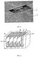
- FIG. 3shows a scanning electron microscope (SEM) photograph of a micromachined comb-drive structure fabricated from single crystal silicon.
- the electrodes of the comb-drive structure of the illustrated structureare isolated using the junction isolation method.
- the junction isolation methodis described, for example, in S. Lee, S. Park and D. Cho, “The Surface/Bulk Micromachining (SBM) Process: A New Method for Fabricating Released Microelectromechanical Systems in Single Crystal Silicon,” IEEE/ASME J. Microelectromechanical Systems , Vol. 8, No. 4, December 1999.
- the junction isolation methodforms a junction diode on a lightly doped N-type or P-type wafer. Applying a reverse biased voltage to the junction diode isolates the junction electrode from the substrate.
- the silicon substrate 10is lightly doped P-type and the lighter parts 12 , including the comb-drive structure, are highly doped with phosphorus, such that a PN junction between the silicon substrate 10 (P-type) and the electrode 12 (N-type) is formed.
- the electrodes 12are electrically isolated from the silicon substrate 10 .
- This methodhas the advantage that the isolation steps are done before the micromechanical structure is fabricated, so that the structure can be fabricated in a relatively easy manner.
- the methodhas disadvantage that the depth of the PN junction often cannot be made sufficiently deep, so that this process usually is not readily applied to a tall structure having a high aspect ratio.
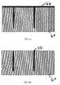
- FIG. 4is a structure formed by yet another conventional isolation method, the trench oxide isolation method, described in the following references: U.S. Pat. No. 5,930,595; U. Sridhar et al., “Trench Oxide Isolated Single Crystal Silicon Micromachined Accelerometer,” IEEE IEDM , San Francisco Calif., Dec. 6-9, 1998. pp. 475-478; and S. Lee, S. Park, D. Cho and Y. Oh “Surface/Bulk Micromachining (SBM) Process and Deep Trench Oxide Isolation Method for MEMS”, IEEE IEDM , Washington, D.C., Dec. 5-8, 1999. pp. 701-704.
- SBMSurface/Bulk Micromachining
- This trench isolation methodincludes forming U-shaped trenches 14 on a silicon substrate 16 , forming thermal oxide layers 18 and depositing oxide layers 20 on all sides of the structure where the trenches are formed.
- the oxide films 18 , 20 filling the trenchesattach the electrode structures 22 , 24 to the silicon substrate 16 through the respective sidewalls so that the oxide films support the electrodes and tethered structures.
- the oxide filmselectrically isolate the electrodes from each other and from the substrate.
- This methodhas the advantage that the method can be applied to a tall structure having a high aspect ratio.
- separate photolithography and etching stepsundesirably are required to form a metal layer on the electrode, which is required for wire bonding the electrode to a package.
- Two different release processesare required: one to separate the electrode component from the substrate and a second to separate the structure part from the substrate.
- the trenches between the sidewalls of the electrode and the sidewalls of the substrategenerally cannot be made arbitrarily large, as would be desired to achieve a small parasitic capacitance, without sacrificing the structural rigidity of the trench filled oxide layers that support the structure and electrodes.
- the insulation layers the conventional trench isolation method deposits on the sides of the electrodeare used to support the structure and electrodes. Therefore, the insulation layers must be deposited between the electrode and the substrate, which in turn, results in severe limitations on electrode shapes that can be fabricated. In particular, it is difficult to fabricate an electrode in an “island” shape. Therefore, it can be appreciated that this method is difficult to use in microelectromechanical systems having a complicated electrode arrangement. Those skilled in the art can appreciate the need for a simpler isolation method.
- An aspect of the present inventionis an isolation method for microelectromechanical systems.
- the methodincludes etching a trench into a substrate, the trench having a depth at least as large as a sum of a thickness of an electrode to be formed and a separation distance between the electrode to be formed and an underlying surface of the substrate, the trench formed in an interior portion of the electrode to be formed.
- An insulation layeris formed within the trench.
- the electrodeis patterned by etching around a periphery of the electrode to a depth greater than a thickness of the electrode.
- the substrateis laterally etched below the electrode, to at least partially separate the electrode from the underlying substrate, leaving the insulation layer in at least part of the trench so that the insulation layer anchors the electrode to the substrate and provides support for the electrode.
- Another aspect of the present inventionis an isolation method for microelectromechanical systems made of silicon, using deep trench insulation layers.
- the isolation methodincludes forming trenches to have a depth larger than the sum of the thickness of electrodes to be formed and a vertical separation between the electrodes to be formed and the underlying substrate.
- the trenchesare formed in middle portions of the electrodes to be formed.
- the trenchesare filled with insulation and the electrodes and etch holes are patterned.
- the electrodesare separated from the underlying substrate by etching the substrate laterally, below the electrodes and through the etch holes, so that the insulation in the trenches provides support for the electrodes spaced from the underlying substrate.
- a microelectromechanical systemincluding a substrate having two electrodes formed above a recessed surface of the substrate, each of the electrodes have a lower surface facing and spaced from the recessed surface. Trenches extend at least partially through corresponding ones of the electrodes and into the substrate at positions corresponding to the trenches through the electrodes. The trenches are formed in an interior portion of the electrodes. Insulation fills each of the trenches within the electrodes and the corresponding trenches in the substrate, the insulation extending between the electrodes and the substrate to support the electrodes and anchor the electrodes to the substrate. A peripheral separation between the electrodes is at least partially filled with air.
- FIG. 1shows a process flow of the SCREAM isolation method.
- FIG. 2shows a process flow of the SOI wafer insulation method.
- FIG. 3shows an SEM photograph of micromachined comb-drive structure including the junction isolation method.
- FIG. 4is a schematic diagram illustrating a trench oxide isolation method.
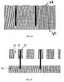
- FIG. 5shows a schematic view of an electrode with etch holes and insulation layer filled trenches according to a preferred embodiment of the present invention.
- FIGS. 6 a to 6 gshow a process flow example for fabricating the isolated electrode of FIG. 5, shown along the cross section 6 - 6 ′ in FIG. 5;
- FIG. 7shows a schematic view of an electrode with etch holes and insulation layer filled trenches, according to another preferred embodiment of the present invention.
- FIGS. 8 a to 8 gshow an exemplary process flow for fabricating the isolated electrode in FIG. 7, shown along the cross section 8 - 8 ′ in FIG. 5.
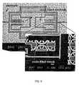
- FIG. 9shows an SEM photograph of an electrically isolated comb-drive resonator fabricated of single crystal silicon made by the process steps in FIGS. 5 and 6 a to 6 g.
- FIG. 10shows an SEM photograph of another electrically isolated comb-drive resonator fabricated of single crystal silicon made by the process steps in FIGS. 5 and 6 a to 6 g.
- Particularly preferred embodiments of the present inventionprovide an isolation method for microelectromechanical systems, preferably made on a silicon substrate, using a deep trench insulation layer.
- a preferred methodforms one or more trenches in an interior portion of a structure to be isolated and fills the one or more trenches with an insulating layer.
- Subsequent patterning processesdefine the electrodes, the structure and etch holes in the interior of the structure.
- the electrodes and the structureare separated from the underlying substrate by laterally etching the substrate, below the electrodes and structure and the etch holes. The laterally etching does not etch the insulation layer so that the insulation layers anchor the electrodes and the structure to the underlying substrate and the insulation layer supports the electrodes and the structure.
- the trenchesare formed to have a depth larger than the sum of the thickness of the electrode to be formed and the vertical separation distance between the electrode to be formed and the underlying substrate. In many instances, the trenches are formed in a middle portion of the electrode to be formed.
- the pattern etching steps for the trenches, electrodes, structure, and etch holes on the silicon substrateare preferably an anisotropic, reactive ion etching processes.
- the lateral “release” etching step that separates the structure and electrode portions from the underlying substrateis performed according to the following guidelines. If the substrate is a (111)-oriented silicon wafer, the release etching is preferably performed using an alkaline solution having preferentially slow etch rates for ⁇ 111 ⁇ planes. A description of such a release etch is described in U.S. Pat. No. 6,150,275, which patent is hereby incorporated by reference in its entirety. On the other hand, if the substrate is a silicon wafer of (100) or (110) orientation, the lateral release etching is performed using an isotropic etching gas such as XeF 2 , or the like.
- Practice of preferred aspects of the present inventionprovide an isolation method for microelectromechanical systems that does not require two different release steps to separate the electrode part from the substrate and to separate the micromechanical structure part from the substrate.
- Preferred implementationsprovide an isolation method for microelectromechanical systems, which does not require separate photolithography and etching steps for metallization of electrodes.
- the deep trench isolationdoes not limit the separation distance between the sidewalls of the electrode and the sidewalls of the substrate.
- the insulating layer of the trench isolation structuredoes not attach the electrode to the sidewalls of the substrate, thereby allowing the fabrication of electrodes in arbitrary shapes, including an “island” shape.
- FIG. 5shows a schematic plan view of an electrode with etch holes and insulation layer filled trenches.
- FIGS. 6 a to 6 gshow a process flow example of fabricating the isolated electrode in FIG. 5, shown along the cross section 6 - 6 ′ illustrated in FIG. 5.
- FIG. 5shows trenches 52 filled with insulation layers so that the combined structure supports the silicon electrode 51 and tethers the electrode to a surface of the underlying substrate.
- the insulation layeris not present between the sides of the electrode 51 and the sides of the substrate, but is instead provided in one or more trenches in the interior or middle part of the electrode.
- Etch holes 53preferably are also formed in the interior part and around the perimeter of the electrodes 51 .
- the etch holes 53electrically isolate the electrodes from the silicon substrate and from other electrodes by air gaps.
- a transverse or lateral dimension of an etch holemay be made arbitrarily large, thereby reducing the parasitic capacitance between adjacent electrodes. Capacitance across an air gap is inversely proportional to the gap distance.
- FIG. 5A preferred process for fabricating the structure shown in FIG. 5 is explained with reference to FIGS. 6 a to 6 g .
- the illustrated structureis formed on a highly doped, low resistivity, conducting silicon wafer 60 .
- An oxide layer 62or other material suitable for forming an etch mask for etching deep trenches, is deposited and patterned on the silicon wafer substrate as shown in FIG. 6 a .
- Deep trenches 64are etched into the silicon substrate. The depth of the deep trenches is selected to be greater than the sum of the thickness of the electrode to be formed and the vertical separation distance between the electrode to be formed and the underlying substrate, as shown in FIG. 6 b .
- the deep trenches 64 shown in FIG. 6 bare filled with insulation layers 66 as shown in FIG. 6 c .
- the insulation layer 66 used at this timemay be an oxide layer, a nitride layer, or a combination of oxide and nitride layers.
- the insulation layer 66 that remains on the top surface of the silicon waferis removed as shown in FIG. 6 d , followed by deposition and patterning for the second masking material.
- the second masking materialis patterned to form an etch mask 68 for the structure and electrodes shown in FIG. 6 e .
- the structure and the electrodes 51are patterned and separated from the silicon substrate as well as adjacent electrodes as shown in FIG. 6 f .
- a metal film 70is deposited on the top surfaces of the structure and electrodes as shown in FIG. 6 g .
- 6 fpresently comprise the steps of patterning parts to be separated from the adjacent parts of the silicon substrate and from the adjacent electrodes by reactive ion etching; and separating the part to be separated from the underlying silicon substrate by lateral silicon etching, including alkaline wet etching and XeF 2 gaseous etching.
- the structure and the electrodes 51are separated from the silicon substrate 50 at its sides and at its bottom. Insulation layers 52 fill the deep trenches and pass through the middle portions of the electrode 51 and into the underlying substrate 50 to anchor the electrode 51 to the substrate 50 and to support the electrode 51 .
- the electrode 51can be separated from the substrate and other electrodes, thereby assuming an “island” shape, so that the electrode 51 is electrically insulated from the substrate and other electrodes by the insulating layers and air gaps.
- insulation layersare not formed on the sides of the electrode 51 but are instead formed within the interior or middle of the electrode 51 and anchored to the substrate 50 . Consequently, there is no need to insert insulation layers between the electrode and the sidewalls of the silicon substrate. This allows the structure and electrodes to be fabricated in many different shapes. Hence, the isolation method according to the present invention can be applied in fabricating complex structures where the arrangement of electrodes may be very complicated.
- the metal layer 70is deposited on the surfaces of the structure and electrodes formed by the release step as shown in FIG. 6 g , and thus there is no need to carry out different photolithography and etching steps for patterning the metal layer 70 .
- FIG. 7shows a schematic view of an electrode with etch holes and insulation layer filled trenches, representing another preferred embodiment of the present invention.
- FIGS. 8 a to 8 gshow an exemplary process flow example for fabricating the isolated electrode in FIG. 7, shown along the cross section 8 - 8 ′ in FIG. 7.
- trenches 72are formed through the electrode and filled with insulation layers to support the silicon electrode 71 .
- the insulation layersneed not be formed between the sides of the electrode 71 and the sides of the substrate. Rather the insulation layers can be formed entirely in the interior of the electrode.
- Etch holes 73are also formed in the middle part and around the perimeter of the electrodes 71 . By forming these etch holes 73 , the electrodes are electrically isolated from the silicon substrate and from other electrodes by air gaps. A lateral or transverse dimension of an etch hole may be made arbitrarily large, thereby allowing a small parasitic capacitance to exist between the electrodes insulated and supported by this technique. As noted earlier, capacitance across an air gap is inversely proportional to the gap distance.
- FIGS. 8 a to 8 gThe process flow as shown in FIGS. 8 a to 8 g is identical to that in FIGS. 6 a to 6 g , with the exception that the patterns of the structure and electrodes are different. As such, details of the process flow are not repeated here, but can instead be understood from the above description of the process of FIG. 6.
- FIG. 8 fillustrates the result of the FIG. 8 process and a cross section through the illustration of FIG. 7.
- the structure and the electrodes 71are separated from the silicon substrate at the electrodes' sides and at the electrodes' bottom.
- the insulation layers 82 that fill the deep trenches passing through the middle of the electrode 81 and are anchored to the substrate 80support the electrode 81 .
- the electrode 81can be separated from the substrate and other electrodes, while assuming an “island” shape, such that the electrode 81 is electrically insulated from the substrate and other electrodes by the air gap.
- the insulation layersare not formed on the sides of the electrode 81 but are instead formed through interior portions of the electrode 81 to anchor the electrode to the substrate 80 . There is consequently no need to insert insulation layers between the electrodes and the sidewalls of the silicon substrate. This allows the structure and electrodes to be fabricated in many different shapes. Hence, the isolation method according to the present invention can be applied in fabricating complex structures where the arrangement of electrodes may be very complicated.
- the structure and electrodesare separated from the substrate in a single release step as shown in FIG. 8 f , so that there is no need to perform separate release steps for releasing the structure and releasing the electrodes.
- the metal layeris deposited on the surfaces of the structure and electrodes formed by the release step as shown in FIG. 8 g and thus there is no need to carry out different photolithography and etching steps for patterning of metal layer.
- isolation methods of the present inventioncan be applied to various silicon microelectromechanical sensors and actuators, including but not limited to, accelerometers, gyroscopes, and mirror arrays.
- FIG. 9shows an SEM photograph of a comb-drive resonator having the honey-comb patterned insulating pillars as shown in FIG. 5 and FIGS. 6 a to 6 g .
- FIG. 10shows an SEM photograph of another comb-drive resonator having the insulating wall structures as shown in FIG. 7 and FIGS. 8 a to 8 g .
- These comb-drive resonators shown in FIGS. 9 and 10are electrically insulated and have been electrostatically driven in atmospheric pressure.
Landscapes
- Engineering & Computer Science (AREA)
- Computer Hardware Design (AREA)
- Microelectronics & Electronic Packaging (AREA)
- Physics & Mathematics (AREA)
- Condensed Matter Physics & Semiconductors (AREA)
- General Physics & Mathematics (AREA)
- Manufacturing & Machinery (AREA)
- Power Engineering (AREA)
- Micromachines (AREA)
- Pressure Sensors (AREA)
Abstract
Description
- The present application claims priority under 35 U.S.C. § 119 from Korean patent application No. 2000-1550, “Isolation Method for Single Crystalline Silicon in Micromachining Using Deep Trench Insulation Layers,” filed with the Korean Industrial Property Office on Jan. 13, 2000.[0001]
- 1. Field of the Invention[0002]
- The present invention relates generally to microelectromechanical systems and more specifically to such systems that include an electrical isolation structure and to methods for electrically isolating a part of a single crystalline silicon microstructure using a deep trench insulation layer in a microelectromechanical system.[0003]
- 2. Description of the Related Art[0004]
- Microelectromechanical systems include component structures with typical minimum dimensions on the order of a micron where the component structures can have elaborate shapes and perform a variety of complex functions. The component structures of microelectromechnical systems are formed on a semiconductor or glass substrate. Microelectromechanical systems include devices such as accelerometers that sense the acceleration of a moving object, gyroscopes that sense the angular rate of a rotating object and mirror arrays that deflect light in fiber optic communication and display applications. Micromachining techniques are used to fabricate the very small structures that are integrated with electrical parts on the semiconductor or glass substrate. The techniques used to fabricate these microelectromechanical systems are largely based on semiconductor device fabricating technology, including photolithography, thin film deposition, etching, impurity doping by diffusion and ion implantation, electroplating and wafer bonding.[0005]
- Microelectromechanical systems often include moving parts that are suspended from or tethered to an underlying substrate and that can move independently of the underlying substrate. Microelectromechanical systems also include electrodes that are electrically isolated to allow the electrodes, for example, to measure electrical signals flowing in the moving parts of the system. Other types of electrodes are used to apply electrical signals to the moving parts of the system; this application also requires that the electrodes be electrically isolated. Electrodes have to be electrically isolated from one another, and also from the substrate on which the electrodes and the tethered moving parts are fabricated. Many methods for electrically isolating a part of a microelectromechanical system from other parts of the system have been studied.[0006]
- FIG. 1 shows process steps in the conventional isolation process known as the single crystalline reactive etching and metallization (hereinafter, referred to as “SCREAM”) process. The SCREAM isolation method fabricates a structure by the SCREAM micromachining technique in the manner discussed in U.S. Pat. No. 5,563,343; U.S. Pat. No. 5,198,390; and K. A. Shaw, Z. L. Zhang, and N. C. MacDonald, “SCREAM I: A Single Mask, Single-Crystal Silicon, Reactive Ion Etching Process for Microelectromechanical Structures,”[0007]Sensors and Actuators A, Vol. 40, pp. 63, 1994. Plasma enhanced chemical vapor deposition (hereinafter, “PECVD”) covers all surfaces of a micromachined structure with an oxide film. Selective deposition of metal film on the structure forms electrodes and electrically conducting paths on top of the PECVD oxide film. In this SCREAM process, electrical isolation of the electrodes is achieved by depositing the metal film only on the top and the side surfaces of microelectromechanical structures.
- The SCREAM isolation method has the advantage of being relatively simple in not requiring separate photolithography and etching steps once the structure is fabricated using the SCREAM micromachining technique. On the other hand, the coverage achieved in the deposition of the metal film is generally poor and hence the SCREAM isolation method typically cannot be applied to tall structures having a high aspect ratio. It should be noted that, if a metal or other material is deposited that has good step coverage, such as metal films deposited by low pressure chemical vapor deposition (hereinafter, referred to as “LPCVD”), all electrodes and microelectromechanical parts are electrically connected, and hence, electrical isolation is not achieved.[0008]
- FIG. 2 shows the silicon on oxide insulator (hereinafter, “SOI”) wafer method, used in forming the microelectromechanical systems described in the following references: B. Diem, et al., “SOI(SIMOX) as a Substrate for Surface Micromachining of Single Crystalline Silicon Sensors and Actuators,”[0009]Tech. Dig.7th Int. Conf. Solid-State Sensors and Actuators(Transducers '93), Yokohama, Japan, 1993, pp. 233-236; and C. Marxer, et al., “Vertical Mirrors Fabricated by Deep Reactive Ion Etching for Fiber-Optic Switching Applications,”IEEE/ASME Journal of Microelectromchanical Systems, Vol. 6, No. 3, pp. September 1997. In the SOI wafer method, the portion of the wafer on top of the buried oxide layer (hereinafter, the “device layer”) is highly doped, conducting silicon. Since all structures and electrodes are fabricated in the device layer and are defined by etching the device layer to the buried oxide layer, electrical isolation of the resulting electrodes is achieved automatically. On the other hand, SOI wafers are generally expensive and the residual stress created by the buried oxide layer can warp and change the shape of microelectromechanical structures. In addition, the micromachined portions of the device layer silicon near the oxide interface can have roughened features (known as the “footing” effect) when the structures and electrodes are formed in a deep plasma etching process. Another disadvantage of the SOI process is that the as-manufactured wafer has an established thickness of the oxide film and the device layer and these thicknesses cannot be modified once a wafer is manufactured.
- FIG. 3 shows a scanning electron microscope (SEM) photograph of a micromachined comb-drive structure fabricated from single crystal silicon. The electrodes of the comb-drive structure of the illustrated structure are isolated using the junction isolation method. The junction isolation method is described, for example, in S. Lee, S. Park and D. Cho, “The Surface/Bulk Micromachining (SBM) Process: A New Method for Fabricating Released Microelectromechanical Systems in Single Crystal Silicon,”[0010]IEEE/ASME J. Microelectromechanical Systems, Vol. 8, No. 4, December 1999. The junction isolation method forms a junction diode on a lightly doped N-type or P-type wafer. Applying a reverse biased voltage to the junction diode isolates the junction electrode from the substrate. Referring to FIG. 3, the
silicon substrate 10 is lightly doped P-type and the lighter parts12, including the comb-drive structure, are highly doped with phosphorus, such that a PN junction between the silicon substrate10 (P-type) and the electrode12 (N-type) is formed. In this case, if a reverse bias voltage is applied to the PN junction, the electrodes12 are electrically isolated from thesilicon substrate 10. This method has the advantage that the isolation steps are done before the micromechanical structure is fabricated, so that the structure can be fabricated in a relatively easy manner. On the other hand, the method has disadvantage that the depth of the PN junction often cannot be made sufficiently deep, so that this process usually is not readily applied to a tall structure having a high aspect ratio. - FIG. 4 is a structure formed by yet another conventional isolation method, the trench oxide isolation method, described in the following references: U.S. Pat. No. 5,930,595; U. Sridhar et al., “Trench Oxide Isolated Single Crystal Silicon Micromachined Accelerometer,”[0011]IEEE IEDM, San Francisco Calif., Dec. 6-9, 1998. pp. 475-478; and S. Lee, S. Park, D. Cho and Y. Oh “Surface/Bulk Micromachining (SBM) Process and Deep Trench Oxide Isolation Method for MEMS”,IEEE IEDM, Washington, D.C., Dec. 5-8, 1999. pp. 701-704. This trench isolation method includes forming U-shaped
trenches 14 on a silicon substrate16, formingthermal oxide layers 18 and depositingoxide layers 20 on all sides of the structure where the trenches are formed. The oxide films18,20 filling the trenches attach theelectrode structures - This method has the advantage that the method can be applied to a tall structure having a high aspect ratio. On the other hand, separate photolithography and etching steps undesirably are required to form a metal layer on the electrode, which is required for wire bonding the electrode to a package. Two different release processes are required: one to separate the electrode component from the substrate and a second to separate the structure part from the substrate. The trenches between the sidewalls of the electrode and the sidewalls of the substrate generally cannot be made arbitrarily large, as would be desired to achieve a small parasitic capacitance, without sacrificing the structural rigidity of the trench filled oxide layers that support the structure and electrodes.[0012]
- Additionally, the insulation layers the conventional trench isolation method deposits on the sides of the electrode are used to support the structure and electrodes. Therefore, the insulation layers must be deposited between the electrode and the substrate, which in turn, results in severe limitations on electrode shapes that can be fabricated. In particular, it is difficult to fabricate an electrode in an “island” shape. Therefore, it can be appreciated that this method is difficult to use in microelectromechanical systems having a complicated electrode arrangement. Those skilled in the art can appreciate the need for a simpler isolation method.[0013]
- An aspect of the present invention is an isolation method for microelectromechanical systems. The method includes etching a trench into a substrate, the trench having a depth at least as large as a sum of a thickness of an electrode to be formed and a separation distance between the electrode to be formed and an underlying surface of the substrate, the trench formed in an interior portion of the electrode to be formed. An insulation layer is formed within the trench. The electrode is patterned by etching around a periphery of the electrode to a depth greater than a thickness of the electrode. The substrate is laterally etched below the electrode, to at least partially separate the electrode from the underlying substrate, leaving the insulation layer in at least part of the trench so that the insulation layer anchors the electrode to the substrate and provides support for the electrode.[0014]
- Another aspect of the present invention is an isolation method for microelectromechanical systems made of silicon, using deep trench insulation layers. The isolation method includes forming trenches to have a depth larger than the sum of the thickness of electrodes to be formed and a vertical separation between the electrodes to be formed and the underlying substrate. The trenches are formed in middle portions of the electrodes to be formed. The trenches are filled with insulation and the electrodes and etch holes are patterned. The electrodes are separated from the underlying substrate by etching the substrate laterally, below the electrodes and through the etch holes, so that the insulation in the trenches provides support for the electrodes spaced from the underlying substrate.[0015]
- Yet another aspect of the present invention provides a microelectromechanical system including a substrate having two electrodes formed above a recessed surface of the substrate, each of the electrodes have a lower surface facing and spaced from the recessed surface. Trenches extend at least partially through corresponding ones of the electrodes and into the substrate at positions corresponding to the trenches through the electrodes. The trenches are formed in an interior portion of the electrodes. Insulation fills each of the trenches within the electrodes and the corresponding trenches in the substrate, the insulation extending between the electrodes and the substrate to support the electrodes and anchor the electrodes to the substrate. A peripheral separation between the electrodes is at least partially filled with air.[0016]
- FIG. 1 shows a process flow of the SCREAM isolation method.[0017]
- FIG. 2 shows a process flow of the SOI wafer insulation method.[0018]
- FIG. 3 shows an SEM photograph of micromachined comb-drive structure including the junction isolation method.[0019]
- FIG. 4 is a schematic diagram illustrating a trench oxide isolation method.[0020]
- FIG. 5 shows a schematic view of an electrode with etch holes and insulation layer filled trenches according to a preferred embodiment of the present invention.[0021]
- FIGS. 6[0022]ato6gshow a process flow example for fabricating the isolated electrode of FIG. 5, shown along the cross section6-6′ in FIG. 5;
- FIG. 7 shows a schematic view of an electrode with etch holes and insulation layer filled trenches, according to another preferred embodiment of the present invention.[0023]
- FIGS. 8[0024]ato8gshow an exemplary process flow for fabricating the isolated electrode in FIG. 7, shown along the cross section8-8′ in FIG. 5.
- FIG. 9 shows an SEM photograph of an electrically isolated comb-drive resonator fabricated of single crystal silicon made by the process steps in FIGS. 5 and 6[0025]ato6g.
- FIG. 10 shows an SEM photograph of another electrically isolated comb-drive resonator fabricated of single crystal silicon made by the process steps in FIGS. 5 and 6[0026]ato6g.
- Particularly preferred embodiments of the present invention provide an isolation method for microelectromechanical systems, preferably made on a silicon substrate, using a deep trench insulation layer. A preferred method forms one or more trenches in an interior portion of a structure to be isolated and fills the one or more trenches with an insulating layer. Subsequent patterning processes define the electrodes, the structure and etch holes in the interior of the structure. Next the electrodes and the structure are separated from the underlying substrate by laterally etching the substrate, below the electrodes and structure and the etch holes. The laterally etching does not etch the insulation layer so that the insulation layers anchor the electrodes and the structure to the underlying substrate and the insulation layer supports the electrodes and the structure.[0027]
- Most preferably, the trenches are formed to have a depth larger than the sum of the thickness of the electrode to be formed and the vertical separation distance between the electrode to be formed and the underlying substrate. In many instances, the trenches are formed in a middle portion of the electrode to be formed.[0028]
- In some embodiments of the present invention, the pattern etching steps for the trenches, electrodes, structure, and etch holes on the silicon substrate are preferably an anisotropic, reactive ion etching processes. Additionally, according to some embodiments, the lateral “release” etching step that separates the structure and electrode portions from the underlying substrate is performed according to the following guidelines. If the substrate is a (111)-oriented silicon wafer, the release etching is preferably performed using an alkaline solution having preferentially slow etch rates for {111} planes. A description of such a release etch is described in U.S. Pat. No. 6,150,275, which patent is hereby incorporated by reference in its entirety. On the other hand, if the substrate is a silicon wafer of (100) or (110) orientation, the lateral release etching is performed using an isotropic etching gas such as XeF[0029]2, or the like.
- Practice of preferred aspects of the present invention provide an isolation method for microelectromechanical systems that does not require two different release steps to separate the electrode part from the substrate and to separate the micromechanical structure part from the substrate. Preferred implementations provide an isolation method for microelectromechanical systems, which does not require separate photolithography and etching steps for metallization of electrodes. The deep trench isolation does not limit the separation distance between the sidewalls of the electrode and the sidewalls of the substrate. In addition, the insulating layer of the trench isolation structure does not attach the electrode to the sidewalls of the substrate, thereby allowing the fabrication of electrodes in arbitrary shapes, including an “island” shape.[0030]
- Now, further discussion of preferred aspects of an isolation method for a microelectromechanical system using a deep trench insulation layer is provided with reference to the accompanying drawings.[0031]
- FIG. 5 shows a schematic plan view of an electrode with etch holes and insulation layer filled trenches. FIGS. 6[0032]ato6gshow a process flow example of fabricating the isolated electrode in FIG. 5, shown along the cross section6-6′ illustrated in FIG. 5.
- FIG. 5 shows[0033]
trenches 52 filled with insulation layers so that the combined structure supports thesilicon electrode 51 and tethers the electrode to a surface of the underlying substrate. Most preferably, the insulation layer is not present between the sides of theelectrode 51 and the sides of the substrate, but is instead provided in one or more trenches in the interior or middle part of the electrode. Etch holes53 preferably are also formed in the interior part and around the perimeter of theelectrodes 51. The etch holes53 electrically isolate the electrodes from the silicon substrate and from other electrodes by air gaps. A transverse or lateral dimension of an etch hole may be made arbitrarily large, thereby reducing the parasitic capacitance between adjacent electrodes. Capacitance across an air gap is inversely proportional to the gap distance. - A preferred process for fabricating the structure shown in FIG. 5 is explained with reference to FIGS. 6[0034]ato6g. The illustrated structure is formed on a highly doped, low resistivity, conducting
silicon wafer 60. Anoxide layer 62, or other material suitable for forming an etch mask for etching deep trenches, is deposited and patterned on the silicon wafer substrate as shown in FIG. 6a.Deep trenches 64 are etched into the silicon substrate. The depth of the deep trenches is selected to be greater than the sum of the thickness of the electrode to be formed and the vertical separation distance between the electrode to be formed and the underlying substrate, as shown in FIG. 6b. This allows the trenches to extend completely through the electrode, across a gap between the electrode and substrate and into the underlying substrate by a sufficient depth to tether the electrodes. Thedeep trenches 64 shown in FIG. 6bare filled with insulation layers66 as shown in FIG. 6c. The insulation layer66 used at this time may be an oxide layer, a nitride layer, or a combination of oxide and nitride layers. - The insulation layer[0035]66 that remains on the top surface of the silicon wafer is removed as shown in FIG. 6d, followed by deposition and patterning for the second masking material. The second masking material is patterned to form an
etch mask 68 for the structure and electrodes shown in FIG. 6e. The structure and theelectrodes 51 are patterned and separated from the silicon substrate as well as adjacent electrodes as shown in FIG. 6f. Subsequently, ametal film 70 is deposited on the top surfaces of the structure and electrodes as shown in FIG. 6g. The patterning and separating steps as shown in FIG. 6fpresently comprise the steps of patterning parts to be separated from the adjacent parts of the silicon substrate and from the adjacent electrodes by reactive ion etching; and separating the part to be separated from the underlying silicon substrate by lateral silicon etching, including alkaline wet etching and XeF2gaseous etching. - As shown in FIG. 6[0036]f, the structure and the
electrodes 51 are separated from thesilicon substrate 50 at its sides and at its bottom. Insulation layers52 fill the deep trenches and pass through the middle portions of theelectrode 51 and into the underlyingsubstrate 50 to anchor theelectrode 51 to thesubstrate 50 and to support theelectrode 51. By this process, theelectrode 51 can be separated from the substrate and other electrodes, thereby assuming an “island” shape, so that theelectrode 51 is electrically insulated from the substrate and other electrodes by the insulating layers and air gaps. - As noted, insulation layers are not formed on the sides of the[0037]
electrode 51 but are instead formed within the interior or middle of theelectrode 51 and anchored to thesubstrate 50. Consequently, there is no need to insert insulation layers between the electrode and the sidewalls of the silicon substrate. This allows the structure and electrodes to be fabricated in many different shapes. Hence, the isolation method according to the present invention can be applied in fabricating complex structures where the arrangement of electrodes may be very complicated. - Furthermore, because the structure and electrodes are separated from the substrate in a single release step as shown in FIG. 6[0038]f, there is no need to perform separate release steps for releasing the structure and releasing the electrodes. This represents a process simplification that should yield a cost reduction.
- Additionally, the[0039]
metal layer 70 is deposited on the surfaces of the structure and electrodes formed by the release step as shown in FIG. 6g, and thus there is no need to carry out different photolithography and etching steps for patterning themetal layer 70. - FIG. 7 shows a schematic view of an electrode with etch holes and insulation layer filled trenches, representing another preferred embodiment of the present invention. FIGS. 8[0040]ato8gshow an exemplary process flow example for fabricating the isolated electrode in FIG. 7, shown along the cross section8-8′ in FIG. 7.
- As shown in FIG. 7,[0041]
trenches 72 are formed through the electrode and filled with insulation layers to support thesilicon electrode 71. As with the previous discussion, the insulation layers need not be formed between the sides of theelectrode 71 and the sides of the substrate. Rather the insulation layers can be formed entirely in the interior of the electrode. Etch holes73 are also formed in the middle part and around the perimeter of theelectrodes 71. By forming these etch holes73, the electrodes are electrically isolated from the silicon substrate and from other electrodes by air gaps. A lateral or transverse dimension of an etch hole may be made arbitrarily large, thereby allowing a small parasitic capacitance to exist between the electrodes insulated and supported by this technique. As noted earlier, capacitance across an air gap is inversely proportional to the gap distance. - The process flow as shown in FIGS. 8[0042]ato8gis identical to that in FIGS. 6ato6g, with the exception that the patterns of the structure and electrodes are different. As such, details of the process flow are not repeated here, but can instead be understood from the above description of the process of FIG. 6.
- The cross section of FIG. 8[0043]fillustrates the result of the FIG. 8 process and a cross section through the illustration of FIG. 7. The structure and the
electrodes 71 are separated from the silicon substrate at the electrodes' sides and at the electrodes' bottom. The insulation layers82 that fill the deep trenches passing through the middle of the electrode81 and are anchored to the substrate80 support the electrode81. - In addition, the electrode[0044]81 can be separated from the substrate and other electrodes, while assuming an “island” shape, such that the electrode81 is electrically insulated from the substrate and other electrodes by the air gap.
- As noted, the insulation layers are not formed on the sides of the electrode[0045]81 but are instead formed through interior portions of the electrode81 to anchor the electrode to the substrate80. There is consequently no need to insert insulation layers between the electrodes and the sidewalls of the silicon substrate. This allows the structure and electrodes to be fabricated in many different shapes. Hence, the isolation method according to the present invention can be applied in fabricating complex structures where the arrangement of electrodes may be very complicated.
- Furthermore, the structure and electrodes are separated from the substrate in a single release step as shown in FIG. 8[0046]f, so that there is no need to perform separate release steps for releasing the structure and releasing the electrodes.
- Additionally, the metal layer is deposited on the surfaces of the structure and electrodes formed by the release step as shown in FIG. 8[0047]gand thus there is no need to carry out different photolithography and etching steps for patterning of metal layer.
- The isolation methods of the present invention can be applied to various silicon microelectromechanical sensors and actuators, including but not limited to, accelerometers, gyroscopes, and mirror arrays.[0048]
- FIG. 9 shows an SEM photograph of a comb-drive resonator having the honey-comb patterned insulating pillars as shown in FIG. 5 and FIGS. 6[0049]ato6g. FIG. 10 shows an SEM photograph of another comb-drive resonator having the insulating wall structures as shown in FIG. 7 and FIGS. 8ato8g. These comb-drive resonators shown in FIGS. 9 and 10 are electrically insulated and have been electrostatically driven in atmospheric pressure.
- Although the present invention has been described in detail with reference to certain presently preferred embodiments, those of ordinary skill in the art will appreciate that various modifications can be made without departing from the invention. Accordingly, the invention is not to be limited to any of the described embodiments thereof but is instead defined by the following claims.[0050]
Claims (17)
Applications Claiming Priority (2)
| Application Number | Priority Date | Filing Date | Title |
|---|---|---|---|
| KR1020000001550AKR100348177B1 (en) | 2000-01-13 | 2000-01-13 | Isolation Method for Single Crystalline Silicon Micro Machining using Deep Trench Dielectric Layer |
| KR2000-1550 | 2000-01-13 |
Publications (2)
| Publication Number | Publication Date |
|---|---|
| US20010013630A1true US20010013630A1 (en) | 2001-08-16 |
| US6472290B2 US6472290B2 (en) | 2002-10-29 |
Family
ID=19638358
Family Applications (1)
| Application Number | Title | Priority Date | Filing Date |
|---|---|---|---|
| US09/756,981Expired - LifetimeUS6472290B2 (en) | 2000-01-13 | 2001-01-09 | Isolation in micromachined single crystal silicon using deep trench insulation |
Country Status (2)
| Country | Link |
|---|---|
| US (1) | US6472290B2 (en) |
| KR (1) | KR100348177B1 (en) |
Cited By (14)
| Publication number | Priority date | Publication date | Assignee | Title |
|---|---|---|---|---|
| WO2003049201A1 (en)* | 2001-12-04 | 2003-06-12 | Origin Energy Solar Pty Ltd | Method of making thin silicon sheets for solar cells |
| US20030224565A1 (en)* | 2002-01-16 | 2003-12-04 | Khalil Najafi | Method of making a thick microstructural oxide layer and device utilizing same |
| US20040097012A1 (en)* | 2000-11-29 | 2004-05-20 | Weber Klaus Johannes | Semiconductor wafer processing to increase the usable planar surface area |
| US6762116B1 (en)* | 2002-06-12 | 2004-07-13 | Zyvex Corporation | System and method for fabricating microcomponent parts on a substrate having pre-fabricated electronic circuitry thereon |
| US20050104163A1 (en)* | 2001-11-29 | 2005-05-19 | Weber Klaus J. | Semiconductor texturing process |
| US6952041B2 (en) | 2003-07-25 | 2005-10-04 | Robert Bosch Gmbh | Anchors for microelectromechanical systems having an SOI substrate, and method of fabricating same |
| US20060121735A1 (en)* | 2002-09-13 | 2006-06-08 | Matthias Aikele | Method for producing insulation structures |
| US20060264067A1 (en)* | 2002-06-14 | 2006-11-23 | Kher Shreyas S | Surface pre-treatment for enhancement of nucleation of high dielectric constant materials |
| US7268646B2 (en) | 2004-03-04 | 2007-09-11 | Robert Bosch Gmbh | Temperature controlled MEMS resonator and method for controlling resonator frequency |
| AU2002349175B2 (en)* | 2001-12-04 | 2008-11-06 | The Australian National University | Method of making thin silicon sheets for solar cells |
| JP2009290155A (en)* | 2008-06-02 | 2009-12-10 | Canon Inc | Structure having plural conductive regions, and process for production thereof |
| CN103033699A (en)* | 2011-09-30 | 2013-04-10 | 意法半导体股份有限公司 | MEMS device, strip test method thereof and test strip thereof |
| US20130122627A1 (en)* | 2011-11-11 | 2013-05-16 | International Business Machines Corporation | Integrated semiconductor devices with single crystalline beam, methods of manufacture and design structure |
| US11279614B2 (en) | 2019-06-28 | 2022-03-22 | Analog Devices, Inc. | Low-parasitic capacitance MEMS inertial sensors and related methods |
Families Citing this family (13)
| Publication number | Priority date | Publication date | Assignee | Title |
|---|---|---|---|---|
| US20040190377A1 (en)* | 2003-03-06 | 2004-09-30 | Lewandowski Robert Stephen | Method and means for isolating elements of a sensor array |
| US7514283B2 (en) | 2003-03-20 | 2009-04-07 | Robert Bosch Gmbh | Method of fabricating electromechanical device having a controlled atmosphere |
| US7075160B2 (en) | 2003-06-04 | 2006-07-11 | Robert Bosch Gmbh | Microelectromechanical systems and devices having thin film encapsulated mechanical structures |
| US6936491B2 (en) | 2003-06-04 | 2005-08-30 | Robert Bosch Gmbh | Method of fabricating microelectromechanical systems and devices having trench isolated contacts |
| US7102467B2 (en) | 2004-04-28 | 2006-09-05 | Robert Bosch Gmbh | Method for adjusting the frequency of a MEMS resonator |
| JP2005354024A (en) | 2004-05-11 | 2005-12-22 | Seiko Epson Corp | Semiconductor substrate manufacturing method and semiconductor device manufacturing method |
| US20070170528A1 (en) | 2006-01-20 | 2007-07-26 | Aaron Partridge | Wafer encapsulated microelectromechanical structure and method of manufacturing same |
| US7508572B2 (en)* | 2006-11-14 | 2009-03-24 | Glimmerglass Networks, Inc. | Charging guard with paschen stacking |
| US8429808B2 (en)* | 2007-12-03 | 2013-04-30 | Kolo Technologies, Inc. | Method for fabrication an electrical transducer |
| US8815653B2 (en)* | 2007-12-03 | 2014-08-26 | Kolo Technologies, Inc. | Packaging and connecting electrostatic transducer arrays |
| US7960285B2 (en)* | 2008-04-18 | 2011-06-14 | Infineon Technologies Ag | Method for the production of a component structure |
| JP7688911B2 (en) | 2018-11-16 | 2025-06-05 | ヴァーモン エス.エー. | Capacitive micromachined ultrasonic transducer and method for manufacturing same |
| US20250187901A1 (en)* | 2023-12-08 | 2025-06-12 | Lawrence Semiconductor Research Laboratory, Inc. | Micro-electro-mechanical systems (mems) having vertical stops and anchor structures |
Family Cites Families (9)
| Publication number | Priority date | Publication date | Assignee | Title |
|---|---|---|---|---|
| US5637539A (en)* | 1996-01-16 | 1997-06-10 | Cornell Research Foundation, Inc. | Vacuum microelectronic devices with multiple planar electrodes |
| SG68630A1 (en) | 1996-10-18 | 1999-11-16 | Eg & G Int | Isolation process for surface micromachined sensors and actuators |
| US5950102A (en)* | 1997-02-03 | 1999-09-07 | Industrial Technology Research Institute | Method for fabricating air-insulated multilevel metal interconnections for integrated circuits |
| US6048774A (en)* | 1997-06-26 | 2000-04-11 | Denso Corporation | Method of manufacturing dynamic amount semiconductor sensor |
| US6075639A (en)* | 1997-10-22 | 2000-06-13 | The Board Of Trustees Of The Leland Stanford Junior University | Micromachined scanning torsion mirror and method |
| KR100300002B1 (en) | 1998-04-01 | 2001-11-22 | 조동일 | Micromachining method using single crystal silicon |
| JP3111977B2 (en)* | 1998-05-15 | 2000-11-27 | 日本電気株式会社 | Method for manufacturing semiconductor device |
| US6281508B1 (en)* | 1999-02-08 | 2001-08-28 | Etec Systems, Inc. | Precision alignment and assembly of microlenses and microcolumns |
| US6306754B1 (en)* | 1999-06-29 | 2001-10-23 | Micron Technology, Inc. | Method for forming wiring with extremely low parasitic capacitance |
- 2000
- 2000-01-13KRKR1020000001550Apatent/KR100348177B1/ennot_activeExpired - Fee Related
- 2001
- 2001-01-09USUS09/756,981patent/US6472290B2/ennot_activeExpired - Lifetime
Cited By (32)
| Publication number | Priority date | Publication date | Assignee | Title |
|---|---|---|---|---|
| US20050272225A1 (en)* | 2000-11-29 | 2005-12-08 | Origin Energy Solar Pty Ltd. | Semiconductor processing |
| US9583668B2 (en) | 2000-11-29 | 2017-02-28 | The Australian National University | Semiconductor device |
| US20040097012A1 (en)* | 2000-11-29 | 2004-05-20 | Weber Klaus Johannes | Semiconductor wafer processing to increase the usable planar surface area |
| US7875794B2 (en) | 2000-11-29 | 2011-01-25 | Transform Solar Pty Ltd | Semiconductor wafer processing to increase the usable planar surface area |
| US7595543B2 (en) | 2000-11-29 | 2009-09-29 | Australian National University | Semiconductor processing method for increasing usable surface area of a semiconductor wafer |
| US7828983B2 (en) | 2001-11-29 | 2010-11-09 | Transform Solar Pty Ltd | Semiconductor texturing process |
| US20050104163A1 (en)* | 2001-11-29 | 2005-05-19 | Weber Klaus J. | Semiconductor texturing process |
| AU2002349175B2 (en)* | 2001-12-04 | 2008-11-06 | The Australian National University | Method of making thin silicon sheets for solar cells |
| US20050070059A1 (en)* | 2001-12-04 | 2005-03-31 | Blakers Andrew William | Method of making thin silicon sheets for solar cells |
| US7169669B2 (en) | 2001-12-04 | 2007-01-30 | Origin Energy Solar Pty. Ltd. | Method of making thin silicon sheets for solar cells |
| US20070093026A1 (en)* | 2001-12-04 | 2007-04-26 | Origin Energy Solar Pty. Ltd. | Method of Making Thin Silicon Sheets for Solar Cells |
| WO2003049201A1 (en)* | 2001-12-04 | 2003-06-12 | Origin Energy Solar Pty Ltd | Method of making thin silicon sheets for solar cells |
| US20030224565A1 (en)* | 2002-01-16 | 2003-12-04 | Khalil Najafi | Method of making a thick microstructural oxide layer and device utilizing same |
| US6962831B2 (en)* | 2002-01-16 | 2005-11-08 | The Regents Of The University Of Michigan | Method of making a thick microstructural oxide layer |
| US6762116B1 (en)* | 2002-06-12 | 2004-07-13 | Zyvex Corporation | System and method for fabricating microcomponent parts on a substrate having pre-fabricated electronic circuitry thereon |
| US20060264067A1 (en)* | 2002-06-14 | 2006-11-23 | Kher Shreyas S | Surface pre-treatment for enhancement of nucleation of high dielectric constant materials |
| US20060121735A1 (en)* | 2002-09-13 | 2006-06-08 | Matthias Aikele | Method for producing insulation structures |
| US7862731B2 (en)* | 2002-09-13 | 2011-01-04 | Conti Temic Microelectronic Gmbh | Method for producing insulation structures |
| US7317233B2 (en) | 2003-07-25 | 2008-01-08 | Robert Bosch Gmbh | Anchors for microelectromechanical systems having an SOI substrate, and method of fabricating same |
| US6952041B2 (en) | 2003-07-25 | 2005-10-04 | Robert Bosch Gmbh | Anchors for microelectromechanical systems having an SOI substrate, and method of fabricating same |
| US7268646B2 (en) | 2004-03-04 | 2007-09-11 | Robert Bosch Gmbh | Temperature controlled MEMS resonator and method for controlling resonator frequency |
| US7427905B2 (en) | 2004-03-04 | 2008-09-23 | Robert Bosch Gmbh | Temperature controlled MEMS resonator and method for controlling resonator frequency |
| JP2009290155A (en)* | 2008-06-02 | 2009-12-10 | Canon Inc | Structure having plural conductive regions, and process for production thereof |
| US20110031568A1 (en)* | 2008-06-02 | 2011-02-10 | Canon Kabushiki Kaisha | Structure having plural conductive regions and process for production thereof |
| US8928042B2 (en) | 2008-06-02 | 2015-01-06 | Canon Kabushiki Kaisha | Structure having plural conductive regions and process for production thereof |
| WO2009148144A3 (en)* | 2008-06-02 | 2010-09-30 | Canon Kabushiki Kaisha | Structure having plural conductive regions and process for production thereof |
| CN103033699A (en)* | 2011-09-30 | 2013-04-10 | 意法半导体股份有限公司 | MEMS device, strip test method thereof and test strip thereof |
| US20130122627A1 (en)* | 2011-11-11 | 2013-05-16 | International Business Machines Corporation | Integrated semiconductor devices with single crystalline beam, methods of manufacture and design structure |
| US9105751B2 (en)* | 2011-11-11 | 2015-08-11 | International Business Machines Corporation | Integrated semiconductor devices with single crystalline beam, methods of manufacture and design structure |
| US9758365B2 (en) | 2011-11-11 | 2017-09-12 | Globalfoundries Inc. | Integrated semiconductor devices with single crystalline beam, methods of manufacture and design structure |
| US11279614B2 (en) | 2019-06-28 | 2022-03-22 | Analog Devices, Inc. | Low-parasitic capacitance MEMS inertial sensors and related methods |
| US11746004B2 (en) | 2019-06-28 | 2023-09-05 | Analog Devices, Inc. | Low-parasitic capacitance MEMS inertial sensors and related methods |
Also Published As
| Publication number | Publication date |
|---|---|
| KR100348177B1 (en) | 2002-08-09 |
| US6472290B2 (en) | 2002-10-29 |
| KR20010073290A (en) | 2001-08-01 |
Similar Documents
| Publication | Publication Date | Title |
|---|---|---|
| US6472290B2 (en) | Isolation in micromachined single crystal silicon using deep trench insulation | |
| US6988408B2 (en) | Surface/bulk micromachined single-crystalline silicon micro-gyroscope | |
| US6433401B1 (en) | Microfabricated structures with trench-isolation using bonded-substrates and cavities | |
| US6569702B2 (en) | Triple layer isolation for silicon microstructure and structures formed using the same | |
| US6951824B2 (en) | Method for manufacturing a micromechanical component and a component that is manufactured in accordance with the method | |
| US6291875B1 (en) | Microfabricated structures with electrical isolation and interconnections | |
| US7943525B2 (en) | Method of producing microelectromechanical device with isolated microstructures | |
| US6960488B2 (en) | Method of fabricating a microfabricated high aspect ratio device with electrical isolation | |
| US6770506B2 (en) | Release etch method for micromachined sensors | |
| US20020125208A1 (en) | MEMS sensor structure and microfabrication process therefor | |
| US7122395B2 (en) | Method of forming semiconductor devices through epitaxy | |
| US7932118B2 (en) | Method of producing mechanical components of MEMS or NEMS structures made of monocrystalline silicon | |
| WO2000016041A3 (en) | Formation of suspended beams using soi substrates, and application to the fabrication of a vibrating gyrometer | |
| US6413793B1 (en) | Method of forming protrusions on single crystal silicon structures built on silicon-on-insulator wafers | |
| EP1770056B1 (en) | Method for manufacturing a micro-electro-mechanical structure | |
| US7618837B2 (en) | Method for fabricating high aspect ratio MEMS device with integrated circuit on the same substrate using post-CMOS process | |
| US7749789B2 (en) | CMOS-compatible bulk-micromachining process for single-crystal MEMS/NEMS devices | |
| US7550358B2 (en) | MEMS device including a laterally movable portion with piezo-resistive sensing elements and electrostatic actuating elements on trench side walls, and methods for producing the same | |
| US8614110B1 (en) | Method for fabricating a dual-crystalline silicon suspension system using pre-fabricated cavities | |
| Lee et al. | Surface/bulk micromachining (SBM) process and deep trench oxide isolation method for MEMS | |
| US20020017133A1 (en) | Surface/bulk micromachined single-crystalline silicon micro-gyroscope | |
| Hofmann et al. | Monolithic three-dimensional single-crystal silicon microelectromechanical systems | |
| KR100405176B1 (en) | An Electrical Isolation Method for Single-Crystalline Silicon MEMS Using Localized SOI Structure | |
| Dan Cho et al. | Tactical Grade MEMS Gyroscopes Fabricated by the SBM Process |
Legal Events
| Date | Code | Title | Description |
|---|---|---|---|
| AS | Assignment | Owner name:CHROMUX TECHNOLOGIES, INC., CALIFORNIA Free format text:ASSIGNMENT OF ASSIGNORS INTEREST;ASSIGNOR:CHO, DONG-IL;REEL/FRAME:011924/0916 Effective date:20010607 | |
| STCF | Information on status: patent grant | Free format text:PATENTED CASE | |
| AS | Assignment | Owner name:CHO, DONG-II, KOREA, REPUBLIC OF Free format text:ASSIGNMENT OF ASSIGNORS INTEREST;ASSIGNOR:CHROMUX TECHNOLOGIES, INC.;REEL/FRAME:013998/0007 Effective date:20030905 | |
| AS | Assignment | Owner name:MICROMECHA, INC., JAPAN Free format text:ASSIGNMENT OF ASSIGNORS INTEREST;ASSIGNOR:CHO, DONG-IL;REEL/FRAME:015953/0545 Effective date:20050321 | |
| AS | Assignment | Owner name:MICROMECHA, INC., KOREA, REPUBLIC OF Free format text:CORRECTED ASSIGNMENT TO CORRECT THE ASSIGNEE ADDRESS ON COVER SHEET PREVIOUSLY RECORDED AT REEL 015953 FRAME 0545;ASSIGNOR:CHO, DONG-IL;REEL/FRAME:016522/0706 Effective date:20050321 | |
| FPAY | Fee payment | Year of fee payment:4 | |
| AS | Assignment | Owner name:BARUN ELECTRONICS CO., LTD., KOREA, REPUBLIC OF Free format text:LICENSE;ASSIGNOR:MICROMECHA, INC.;REEL/FRAME:023304/0173 Effective date:20090922 | |
| FPAY | Fee payment | Year of fee payment:8 | |
| AS | Assignment | Owner name:BARUN ELECTRONICS CO., LTD., KOREA, REPUBLIC OF Free format text:CANCELLATION OF LICENSE AGREEMENT;ASSIGNOR:MICROMECHA, INC.;REEL/FRAME:031377/0459 Effective date:20130930 | |
| FPAY | Fee payment | Year of fee payment:12 |