US20010010952A1 - Color image sensor with embedded microlens array - Google Patents
Color image sensor with embedded microlens arrayDownload PDFInfo
- Publication number
- US20010010952A1 US20010010952A1US09/803,346US80334601AUS2001010952A1US 20010010952 A1US20010010952 A1US 20010010952A1US 80334601 AUS80334601 AUS 80334601AUS 2001010952 A1US2001010952 A1US 2001010952A1
- Authority
- US
- United States
- Prior art keywords
- layer
- microlens
- depositing
- silicon
- nitride
- Prior art date
- Legal status (The legal status is an assumption and is not a legal conclusion. Google has not performed a legal analysis and makes no representation as to the accuracy of the status listed.)
- Granted
Links
Images


Classifications
- H—ELECTRICITY
- H10—SEMICONDUCTOR DEVICES; ELECTRIC SOLID-STATE DEVICES NOT OTHERWISE PROVIDED FOR
- H10F—INORGANIC SEMICONDUCTOR DEVICES SENSITIVE TO INFRARED RADIATION, LIGHT, ELECTROMAGNETIC RADIATION OF SHORTER WAVELENGTH OR CORPUSCULAR RADIATION
- H10F39/00—Integrated devices, or assemblies of multiple devices, comprising at least one element covered by group H10F30/00, e.g. radiation detectors comprising photodiode arrays
- H10F39/80—Constructional details of image sensors
- H—ELECTRICITY
- H10—SEMICONDUCTOR DEVICES; ELECTRIC SOLID-STATE DEVICES NOT OTHERWISE PROVIDED FOR
- H10F—INORGANIC SEMICONDUCTOR DEVICES SENSITIVE TO INFRARED RADIATION, LIGHT, ELECTROMAGNETIC RADIATION OF SHORTER WAVELENGTH OR CORPUSCULAR RADIATION
- H10F39/00—Integrated devices, or assemblies of multiple devices, comprising at least one element covered by group H10F30/00, e.g. radiation detectors comprising photodiode arrays
- H10F39/011—Manufacture or treatment of image sensors covered by group H10F39/12
- H10F39/024—Manufacture or treatment of image sensors covered by group H10F39/12 of coatings or optical elements
- H—ELECTRICITY
- H10—SEMICONDUCTOR DEVICES; ELECTRIC SOLID-STATE DEVICES NOT OTHERWISE PROVIDED FOR
- H10F—INORGANIC SEMICONDUCTOR DEVICES SENSITIVE TO INFRARED RADIATION, LIGHT, ELECTROMAGNETIC RADIATION OF SHORTER WAVELENGTH OR CORPUSCULAR RADIATION
- H10F39/00—Integrated devices, or assemblies of multiple devices, comprising at least one element covered by group H10F30/00, e.g. radiation detectors comprising photodiode arrays
- H10F39/80—Constructional details of image sensors
- H10F39/806—Optical elements or arrangements associated with the image sensors
- H10F39/8063—Microlenses
Definitions
- the present inventionrelates to solid state image sensors. More specifically, the present invention relates to a method for fabricating color image sensors and to a color image sensor fabricated by the method.
- Solid state color image sensorsare used, for example, in video cameras, and are presently realized in a number of forms including charge-coupled devices (CCDs) and CMOS image sensors. These image sensors are based on a two dimensional array of pixels. Each pixel includes color filter located over a sensing element. An array of microlenses located over the color filter focuses light from an optical image through the color filter into the image sensing elements. Each image sensing element is capable of converting a portion of the optical image passed by the color filter into an electronic signal. The electronic signals from all of the image sensing elements are then used to regenerate the optical image on, for example, a video monitor.
- CCDscharge-coupled devices
- CMOS image sensorsare based on a two dimensional array of pixels. Each pixel includes color filter located over a sensing element. An array of microlenses located over the color filter focuses light from an optical image through the color filter into the image sensing elements. Each image sensing element is capable of converting a portion of the optical image passed by
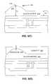
- FIG. 1(A)is a cross-sectional view showing a portion of a conventional color image sensor 10 .
- Color image sensor 10is formed on an n-type semiconductor substrate 11 having a p-well layer 15 .
- An array of photodiodes 20 and charge transfer regions 25are formed in p-well layer 15 , and are covered by a silicon oxide or nitride film 30 .
- a polysilicon electrode 35is located over charge transfer region 25 such that it is surrounded by film 30 .
- a photo-shielding metal layer 40is formed over electrode 35 , and a surface protective coating 45 and a planarization layer 50 are formed over metal layer 40 .
- a color filter layer 60is formed on planarization layer 50 , and an intermediate transparent film 70 is formed over color filter layer 60 .
- a microlens 80 for focusing light beams 85is formed from silicon dioxide (SiO 2 ) or a resin material on intermediate transparent film 70 .
- An air gap 90is provided over microlens 80 , and a glass packaging substrate 95 is located over air gap 90 .
- light beams 85are focused by microlens 80 through color filter layer 60 such that they converge along the focal axis F of microlens 80 to strike photodiode 20 , wherein photoenergy from light beams 85 frees electrons in photodiode 20 .
- photoenergy from light beams 85frees electrons in photodiode 20 .
- a sensor circuit (not shown) of color image sensor 10determines the amount of light received by photodiode 20 by measuring the amount of current generated in charge transfer region 25 .
- Conventional solid-state imaging device 10is designed for light beams 85 whose incident angle is perpendicular to substrate 11 , as shown in FIG. 1(A), before being focused by microlens 80 onto photodiode 20 .
- light beamscan strike microlens 80 at oblique incident angles.
- FIG. 1(B)A consequence of these oblique light beams is shown in FIG. 1(B).
- light beams 87enter microlens 80 at an oblique angle, which directs light beams 87 away from focal axis F such that they converge at the edge of photodiode 20 . Because the photoenergy of light beams 87 is not fully transferred to photodiode 20 , color image sensor 10 is unable to generate an accurate image.
- Standard packaging methodstypically include securing a glass substrate to an IC device using a layer of cement (e.g., epoxy).
- This cementtypically has an index of refraction that is the same as silicon-dioxide and other resins typically used to form microlens 80 and other layers of conventional solid-state imaging device 10 . Therefore, to facilitate proper focusing of the light beams, air gap 90 must be provided between glass packaging substrate 95 and microlens 80 . Because air gap 90 is used in place of cement, the packaging method used to produce conventional solid-state imaging device 10 is non-standard.
- microlens 80 closer to photodiode 20would be to reduce the thickness of the various layers located below microlens 80 .
- a problem with this methodis that the thicknesses of these underlying layers are not easily reduced.
- photo-shielding layer 40is typically formed during the formation of aluminum wiring utilized to transmit signals to and from each pixel of conventional solid-state imaging device 10 . Therefore, the thickness of photo-shielding layer 40 is limited by the wiring specifications.
- Repositioning microlens 80 closer to photodiode 20is further restricted by planarization layer 50 , which is required to provide a flat surface for forming color filter layer 60 and microlens 80 . Therefore, it is not possible to significantly reduce the distance between a surface-mounted microlens 80 and photodiode 20 in conventional solid-state imaging device 10 by reducing the thickness of the layers underlying microlens 80 .
- microlens 80 closer to photodiode 20would be to form microlens So under color filter layer 60 (i.e., between photodiode 20 and color filter layer 60 ).
- This arrangementwould also address the non-standard packaging problem because, with color filter layer 70 -located above microlens 80 , it would be possible to use cement to secure glass packaging substrate 95 according to standard packaging methods.
- forming microlens 80 under color filter layer 60is not practical because, as discussed above, the index of refraction of conventional microlens materials (i.e., resin) is the same as that of other materials typically used to produce conventional solid-state imaging device 10 . Therefore, because air gap 90 must be provided over conventional microlens 80 , it would be very difficult to produce conventional solid-state imaging device 10 with microlens 80 located under color filter layer 60 using conventional microlens materials.
- the present inventionis directed to a method for producing a color CMOS image sensor in which the microlens structure is embedded (i.e., located between the photodiode array and the color filter layer), thereby avoiding the oblique light beam problem, discussed above, because each microlens is located closer to its associated photodiode than in conventional image sensor structures.
- the color filter layeris located above the microlenses and sandwiched between two color transparent layers, conventional image sensor packaging techniques (i.e., applying cement to the upper color transparent layer, then applying a glass substrate) may be utilized to produce color CMOS image sensors.
- an image sensoris produced by depositing a dielectric (e.g., silicon-nitride) layer over an image sensing element (e.g., a photodiode), etching the dielectric layer to form a microlens, and then depositing a protective layer on the microlens, wherein the protective layer has an index of refraction that is different from that of the dielectric.
- a dielectrice.g., silicon-nitride
- an image sensing elemente.g., a photodiode
- the silicon-nitride microlenses of the present inventionmay be embedded under conventional protective materials without eliminating the optical performance of the microlenses.
- other dielectricsmay be used to form the microlens, provided the protective materials formed on the microlens have an index of refraction that is different from that of the dielectric. Because the microlens surface is located below a protective layer, conventional packaging techniques may be used that attach the protective layer to a substrate using cement, thereby reducing manufacturing costs and complexity.
- a color image sensoris produced by depositing a silicon-nitride layer over an image sensing element (e.g., a photodiode), etching the silicon-nitride layer to form a microlens, depositing a color transparent layer on the microlens, and then forming a color filter on the color transparent layer.
- the silicon-nitride microlenshas an index of refraction that is different from the color transparent layer, thereby forming an effective microlens structure that is embedded below the color filter.
- the microlensBy forming the microlens below the color filter, the microlens is positioned closer to the image sensing element, thereby minimizing the oblique light beam problems, described above.
- conventional packaging techniquesmay be used that attach the second color transparent layer to a substrate using cement, thereby reducing manufacturing costs and complexity.
- FIGS. 1 (A) and 1 (B)are cross-sectional side views showing a conventional solid-state imaging device in which normal and oblique light beams are focused by a microlens;
- FIG. 2is a schematic diagram of a solid-state imaging device according to a first embodiment of the present invention
- FIG. 3is a flow diagram showing the basic steps for fabricating the solid-state imaging device shown in FIG. 2;
- FIG. 4(A)is a schematic diagram of a color image sensor device according to a second embodiment of the present invention.
- FIG. 4(B)is a flow diagram showing the basic steps for fabricating the color image sensor device shown in FIG. 4(A);
- FIGS. 5 (A) through 5 (K)are cross-sectional views showing process steps associated with the production of a color imaging device in accordance with another embodiment of the present invention.
- CMOS active-pixel sensorsAPSs
- CMOS active-pixel sensorsAPSs
- the fabrication and operation of CMOS active-pixel sensors (APSs)are described in co-owned and co-pending U.S. application Ser. No. 09/315,893, entitled “Method And Structure For Minimizing White Spots In CMOS Image Sensors”, invented by Yossi Netzer [Docket No. TSL-031], which is incorporated herein by reference.
- the methods and structures described belowmay also be used to produce passive CMOS image sensors and CMOS APSs utilizing photogate light sensitive regions.
- the methods and structuresmay be used to produce CMOS APSs having any number of transistors (e.g., one, four or five).
- the present inventorsbelieve the methods and structures of the present invention may also be used to produce image sensors including MOS pixel arrays.
- image sensoris intended to cover all of these sensor array types.
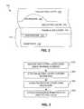
- FIG. 2is a cross-sectional view showing a portion of an image sensor 100 in accordance with an embodiment of the present invention.
- Image sensor 100includes an image sensing element 110 , a dielectric layer 140 formed over image sensing element 110 that is etched to include a microlens 145 , and a protective layer 150 formed on microlens 145 .
- Image sensing element 110includes a photodiode region 114 that is diffused into a silicon substrate 112 , and a passivation layer 118 formed on substrate 112 .
- dielectric layer 140is formed on passivation layer 118 , and has an index of refraction that is different from that of protective layer 150 , thereby allowing microlens 145 to focus light beams passing through protective layer 150 onto photodiode region 114 .
- one or more intermediate layersare formed between passivation layer 118 and dielectric layer 140 .
- FIG. 3is a flow diagram showing the basic steps associated with the formation of image sensor 100 in accordance with the present invention. The process shown in FIG. 3 is performed after image sensing element 110 (FIG. 2) is fabricated using known techniques. At the end of this initial fabrication process, image sensing element 110 includes passivation layer 118 formed over photodiode region 114 .
- the processbegins with the deposition of dielectric layer 140 over passivation layer 118 (Step 310 ).
- the term “rover”is intended to cover both the deposition of dielectric material directly on passivation layer 118 , and the deposition of dielectric material on an intermediate layer(s) formed on passivation layer 118 .
- dielectric materialis silicon-nitride, which has an index of refraction that is higher than silicon-dioxide and other materials typically utilized in CMOS fabrication processes to form protective layer 150 .
- dielectric layer 140is etched to form microlenses 145 (Step 320 ).
- this stepis performed using a reactive-ion etching process according to known techniques. As indicated in FIG. 2, the etching process is controlled such that a portion of dielectric layer 140 remains over passivation layer 118 .
- protective layer 150is formed over microlens 145 and other residual portions of dielectric layer 140 (Step 330 ).
- protective layer 150may be polyimide, resin, or may be packaging adhesive (e.g., epoxy cement) that is applied directly to the upper surface of microlens 145 .
- packaging adhesivee.g., epoxy cement
- protective layer 150may include one or more color transparent layers and color filter layers. In either of these applications, at least the portion of protective layer 150 that contacts microlens 145 is formed using a material having an index of refraction that is different from (i.e., lower than) that of dielectric layer 140 .
- microlens 145is able to effectively focus light beams onto photodiode region 114 . Further, because microlens 145 is formed either directly on or immediately over passivation layer 118 , the distance between microlens 145 and photodiode 114 is minimized, thereby minimizing the problems caused by oblique light beams (discussed above).
- Steps 310 , 320 and 330include the basic process steps for forming an image sensor in accordance with the present invention
- another benefit of image sensor 100is that conventional packaging techniques may be utilized.
- a packaging substratemay be attached to protective layer 150 using a packaging adhesive, such as epoxy cement (Step 340 ).
- a packaging adhesivesuch as epoxy cement
- the packaging substrateis attached directly to protective layer 150 .
- the present inventionfacilitates the use of conventional packaging techniques (i.e., applying cement directly onto protective layer 150 or microlens 145 , and attaching the packaging substrate directly to the cement), thereby reducing packaging costs.
- FIG. 4(A)is a cross-sectional view showing a portion of a color image sensor 200 in accordance with a second aspect of the present invention.
- Color image sensor 200includes an image sensing element 210 , a silicon-nitride layer 240 formed over image sensing element 210 that is etched to include a microlens 245 , a lower (first) color transparent (CT) layer 252 formed on microlens 245 , a color filter layer 255 formed on lower CT layer 252 , and an upper CT layer 257 formed on color filter layer 255 .
- CTcolor transparent
- image sensing element 210includes a photodiode region 214 that is formed in substrate 212 , and a passivation region including silicon-dioxide (SiO 2 ) layer 218 that is formed on substrate 212 .
- SiO 2silicon-dioxide
- Lower CT layer 252 , color filter layer 255 and upper CT layer 257form a color filter structure (protective layer) 250 over microlens 245 that functions, in part, to protect microlens 245 .
- lower CT layer 252is formed from a polymeric material (e.g., negative photoresist based on an acrylic polymer) having an index of refraction that is lower than that of silicon-nitride, thereby allowing 8 microlens 245 to focus light beams passing through lower CT layer 252 onto photodiode region 214 .
- Lower CT layer 252provides both a planar surface and adhesion for color filter layer 255 .
- Color filter layer 255is formed from known materials (e.g., negative photoresist based on an acrylic polymer including color pigments) using known techniques.
- upper CT layer 257is formed from a polymeric material-(e.g., negative photoresist based on an acrylic polymer), and serves both to seal and protect color filter layer 255 .
- FIG. 4(B)is a flow diagram showing the basic steps associated with the formation of color image sensor 200 in accordance with the present invention. The process shown in FIG. 4(B) is performed after image sensing element 210 (FIG. 4(A)) is fabricated using known techniques.
- silicon-nitride layer 240is deposited over silicon-dioxide layer 218 (Step 410 ), and silicon-nitride layer 240 is etched to form microlenses 245 (Step 420 ).
- lower CT layer 252is formed over microlens 245 and other residual portions of silicon-nitride layer 240 , and is then planarized using known techniques (Step 430 ).
- Color filter layer 255is then formed on lower CT layer 252 using known techniques (Step 440 ).
- upper CT layer 257is formed on color filter layer 255 .
- a subsequent step of attaching a packaging substrate to upper CT layer 257 using conventional packaging techniquesis made possible by embedding microlens 245 below color filter structure 250 .
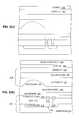
- FIGS. 5 (A) through 5 (K)illustrate the method of producing color image sensor 200 in additional detail.
- FIG. 5(A)is a cross-sectional view showing an initial structure that includes image sensing element 210 .
- Image sensing element 210includes photodiode region 214 and a charge transfer region 215 that are diffused into semiconductor (e.g., silicon) substrate 212 , and base silicon-dioxide (SiO 2 ) layer 218 formed on substrate 212 .
- Metal wires 220are located in base SiO 2 layer 218 that connect to a polysilicon gate region 222 and to charge transfer region 215 , thereby forming select transistor 116 . These structures are fabricated using known techniques.
- FIG. 5(B)illustrates an optional step of depositing a supplemental passivation (SiO 2 ) layer 219 on base SiO 2 layer 218 , and planarizing supplemental SiO 2 layer 219 to provide a flat surface for the dielectric material used to form the embedded microlens.
- the planarized surface provided by supplemental SiO 2 layer 219is not always required (in some cases, base SiO 2 layer 218 has a sufficiently planar surface).
- the thickness of supplemental SiO 2 layer 219is determined by the surface features of base SiO 2 layer 118 (e.g., by exposed wires 220 ), but made as thin as possible so that the subsequently-formed microlens structures are as close to photodiode region 214 as possible.
- FIG. 5(C)illustrates another optional step of depositing an oxi-nitride layer 230 on planarized supplemental SiO 2 layer 219 .
- oxi-nitride layer 230may be formed directly on base SiO 2 layer 219 (i.e., when planarized supplemental SiO 2 layer 219 is not used).
- oxi-nitride layer 230has a thickness in the range of 2.5 to 3.5 microns, and functions as a stress relief layer.
- FIG. 5(D)illustrates a subsequent step of depositing silicon-nitride layer 240 over image sensing element 210 .
- 8 silicon-nitride layer 240is formed on oxi-nitride layer 230 .
- silicon-nitride layer 240may be formed on planarized supplemental SiO 2 layer 219 or base SiO 2 layer 218 if these steps are respectively omitted.
- silicon-nitride layer 240has a thickness in the range of 3 to 5 microns.
- FIG. 5(E)is a cross-sectional view showing the formation of a photoresist portion 510 on silicon-nitride layer 240 and subsequent application of etchant 520 .
- Photoresist portion 510is formed by depositing a layer of photoresist on silicon-nitride layer 240 , exposing the photoresist layer through a mask (either “halftone” or sharp geometry), developing the photoresist layer, and removing portions of the photoresist layer that were exposed. This process is performed using well-known techniques. When a sharp geometry mask is used, photoresist portion 510 is heated to create the required lens-shaped geometry using known techniques.
- the resulting photoresist portion 510has a shape that essentially mirrors than of the desired microlens and is located directly over the portion of silicon-nitride layer 240 used to form the microlens.
- the actual shape of photoresist portion 510depends upon the selectivity of the photoresist material versus that of silicon-nitride layer 240 .
- Etchingis subsequently performed using an anisotropic reactive ion etching (RIE) process that “copies” the lens-like shape of photoresist portion 510 into silicon-nitride layer 240 .
- RIEanisotropic reactive ion etching
- the thinner peripheral portions of photoresist portion 510are removed before the thicker central portions, thereby causing more etching of silicon-nitride layer 240 under the periphery of photoresist portion 510 than under the central portion. Consequently, the lens-like shape of photoresist portion 510 is “copied” into silicon-nitride layer 240 .
- FIG. 5(F)is a cross-sectional view showing silicon-nitride layer 240 after the etching process.
- the resulting shape of microlens 240is essentially the same as that of photoresist portion 510 .
- microlens 245has a peak thickness T 1 in the range of 3 to 5 microns.
- the remaining portions of silicon-nitride layer 240 located adjacent to microlens 245have a thickness T 2 in the range of 0.65 to 1 micron. Residual photoresist material 515 and other polymeric residues are then removed using a solvent 530 .
- FIG. 5(G)is a cross-sectional view showing the subsequent deposition and planarization of lower CT layer 252 on microlens 245 and the remaining portions of silicon-nitride layer 240 .
- lower CT layerpreferably has a thickness T 3 in the range of 1.1 to 1.3 microns.
- FIG. 5(H)is a cross-sectional view showing the subsequent formation of color filter layer 255 on lower CT layer 252 .
- Color filter layer 255is formed using known techniques and has a resulting thickness T 4 in the range of 1.0 to 1.4 microns.
- FIG. 5(I)is a cross-sectional view showing the subsequent formation of upper CT layer 257 on color filter layer 255 .
- Upper CT layer 257is formed from polymeric material or resin, and has a resulting thickness T 5 in the range of 0.8 to 1.1 microns.
- FIGS. 5 (J) and 5 (K)A benefit provided by the fabrication process illustrated in FIGS. 5 (A) through 5 (I) is that standard packaging techniques can be used, thereby reducing overall production costs.
- FIGS. 5 (J) and 5 (K)A simplified representation of these standard packaging techniques is depicted in FIGS. 5 (J) and 5 (K).
- a transparent cement 540e.g., novolac epoxy resin
- FIG. 5(K)e.g., glass
- FIG. 5(K)e.g., glass
- microlens 245is embedded between color filter structure 250 and image sensing element 210 . Therefore, the present invention facilitates the use of standard packaging (i.e., attaching packaging substrate 550 using cement), thereby providing such color CMOS image sensor devices at a lower cost than conventional devices.
Landscapes
- Solid State Image Pick-Up Elements (AREA)
- Transforming Light Signals Into Electric Signals (AREA)
Abstract
Description
- The present invention relates to solid state image sensors. More specifically, the present invention relates to a method for fabricating color image sensors and to a color image sensor fabricated by the method.[0001]
- Solid state color image sensors are used, for example, in video cameras, and are presently realized in a number of forms including charge-coupled devices (CCDs) and CMOS image sensors. These image sensors are based on a two dimensional array of pixels. Each pixel includes color filter located over a sensing element. An array of microlenses located over the color filter focuses light from an optical image through the color filter into the image sensing elements. Each image sensing element is capable of converting a portion of the optical image passed by the color filter into an electronic signal. The electronic signals from all of the image sensing elements are then used to regenerate the optical image on, for example, a video monitor.[0002]
- FIG. 1(A) is a cross-sectional view showing a portion of a conventional[0003]
color image sensor 10.Color image sensor 10 is formed on an n-type semiconductor substrate 11 having a p-well layer 15. An array ofphotodiodes 20 andcharge transfer regions 25 are formed in p-well layer 15, and are covered by a silicon oxide ornitride film 30. Apolysilicon electrode 35 is located overcharge transfer region 25 such that it is surrounded byfilm 30. A photo-shielding metal layer 40 is formed overelectrode 35, and a surfaceprotective coating 45 and aplanarization layer 50 are formed overmetal layer 40. Acolor filter layer 60 is formed onplanarization layer 50, and an intermediatetransparent film 70 is formed overcolor filter layer 60. Amicrolens 80 for focusinglight beams 85 is formed from silicon dioxide (SiO2) or a resin material on intermediatetransparent film 70. Anair gap 90 is provided overmicrolens 80, and aglass packaging substrate 95 is located overair gap 90. - In operation,[0004]
light beams 85 are focused bymicrolens 80 throughcolor filter layer 60 such that they converge along the focal axis F ofmicrolens 80 to strikephotodiode 20, wherein photoenergy fromlight beams 85 frees electrons inphotodiode 20. When a select voltage is applied topolysilicon electrode 35, these freed electrons generate a current incharge transfer region 25. A sensor circuit (not shown) ofcolor image sensor 10 then determines the amount of light received byphotodiode 20 by measuring the amount of current generated incharge transfer region 25. - Conventional solid-[0005]
state imaging device 10 is designed forlight beams 85 whose incident angle is perpendicular tosubstrate 11, as shown in FIG. 1(A), before being focused bymicrolens 80 ontophotodiode 20. However, during actual operation ofcolor image sensor 10, light beams can strikemicrolens 80 at oblique incident angles. A consequence of these oblique light beams is shown in FIG. 1(B). In particular,light beams 87 entermicrolens 80 at an oblique angle, which directslight beams 87 away from focal axis F such that they converge at the edge ofphotodiode 20. Because the photoenergy oflight beams 87 is not fully transferred tophotodiode 20,color image sensor 10 is unable to generate an accurate image. - Another problem associated with conventional solid-[0006]
state imaging device 10 is that non-standard packaging methods are required due to the formation ofmicrolenses 80 overcolor filter layer 60 andintermediate transfer layer 70. Standard packaging methods typically include securing a glass substrate to an IC device using a layer of cement (e.g., epoxy). This cement typically has an index of refraction that is the same as silicon-dioxide and other resins typically used to formmicrolens 80 and other layers of conventional solid-state imaging device 10. Therefore, to facilitate proper focusing of the light beams,air gap 90 must be provided betweenglass packaging substrate 95 andmicrolens 80. Becauseair gap 90 is used in place of cement, the packaging method used to produce conventional solid-state imaging device 10 is non-standard. - It would be possible to avoid the oblique light beam problem (discussed above) by moving[0007]
microlens 80 closer tophotodiode 20, thereby shortening the distance traveled by the light beams betweenmicrolens 80 andphotodiode 20. This shortened distance would reduce the displacement of focused oblique light beams87 (see FIG. 1(B)) relative to the center ofphotodiode 20, thereby transferring more photoenergy from these oblique light beams tophotodiode 20. - One possible method of moving[0008]
microlens 80 closer tophotodiode 20 would be to reduce the thickness of the various layers located belowmicrolens 80. A problem with this method is that the thicknesses of these underlying layers are not easily reduced. First, photo-shielding layer 40 is typically formed during the formation of aluminum wiring utilized to transmit signals to and from each pixel of conventional solid-state imaging device 10. Therefore, the thickness of photo-shielding layer 40 is limited by the wiring specifications. Repositioningmicrolens 80 closer tophotodiode 20 is further restricted byplanarization layer 50, which is required to provide a flat surface for formingcolor filter layer 60 andmicrolens 80. Therefore, it is not possible to significantly reduce the distance between a surface-mountedmicrolens 80 andphotodiode 20 in conventional solid-state imaging device 10 by reducing the thickness of thelayers underlying microlens 80. - Another possible method of moving[0009]
microlens 80 closer tophotodiode 20 would be to form microlens So under color filter layer60 (i.e., betweenphotodiode 20 and color filter layer60). This arrangement would also address the non-standard packaging problem because, with color filter layer70-located abovemicrolens 80, it would be possible to use cement to secureglass packaging substrate 95 according to standard packaging methods. However, formingmicrolens 80 undercolor filter layer 60 is not practical because, as discussed above, the index of refraction of conventional microlens materials (i.e., resin) is the same as that of other materials typically used to produce conventional solid-state imaging device 10. Therefore, becauseair gap 90 must be provided overconventional microlens 80, it would be very difficult to produce conventional solid-state imaging device 10 withmicrolens 80 located undercolor filter layer 60 using conventional microlens materials. - What is needed is a method for fabricating a color image sensor that minimizes the distance between the microlens and photodiode, and minimizes the fabrication and production costs of the color image sensor.[0010]
- The present invention is directed to a method for producing a color CMOS image sensor in which the microlens structure is embedded (i.e., located between the photodiode array and the color filter layer), thereby avoiding the oblique light beam problem, discussed above, because each microlens is located closer to its associated photodiode than in conventional image sensor structures. In addition, because the color filter layer is located above the microlenses and sandwiched between two color transparent layers, conventional image sensor packaging techniques (i.e., applying cement to the upper color transparent layer, then applying a glass substrate) may be utilized to produce color CMOS image sensors.[0011]
- In accordance with a first embodiment of the present invention, an image sensor is produced by depositing a dielectric (e.g., silicon-nitride) layer over an image sensing element (e.g., a photodiode), etching the dielectric layer to form a microlens, and then depositing a protective layer on the microlens, wherein the protective layer has an index of refraction that is different from that of the dielectric. When silicon-nitride is utilized as the dielectric, conventional protective layer materials may be formed on the microlens because the refractive index of silicon-nitride is different from silicon-dioxide and other materials utilized as conventional protective layer materials. Therefore, the silicon-nitride microlenses of the present invention may be embedded under conventional protective materials without eliminating the optical performance of the microlenses. In alternative embodiments, other dielectrics may be used to form the microlens, provided the protective materials formed on the microlens have an index of refraction that is different from that of the dielectric. Because the microlens surface is located below a protective layer, conventional packaging techniques may be used that attach the protective layer to a substrate using cement, thereby reducing manufacturing costs and complexity.[0012]
- In accordance with another embodiment of the present invention, a color image sensor is produced by depositing a silicon-nitride layer over an image sensing element (e.g., a photodiode), etching the silicon-nitride layer to form a microlens, depositing a color transparent layer on the microlens, and then forming a color filter on the color transparent layer. The silicon-nitride microlens has an index of refraction that is different from the color transparent layer, thereby forming an effective microlens structure that is embedded below the color filter. By forming the microlens below the color filter, the microlens is positioned closer to the image sensing element, thereby minimizing the oblique light beam problems, described above. In addition, by forming a second color transparent layer over the color filter, conventional packaging techniques may be used that attach the second color transparent layer to a substrate using cement, thereby reducing manufacturing costs and complexity.[0013]
- The novel aspects of the present invention will be more fully understood in view of the following description and drawings.[0014]
- FIGS.[0015]1(A) and1(B) are cross-sectional side views showing a conventional solid-state imaging device in which normal and oblique light beams are focused by a microlens;
- FIG. 2 is a schematic diagram of a solid-state imaging device according to a first embodiment of the present invention;[0016]
- FIG. 3 is a flow diagram showing the basic steps for fabricating the solid-state imaging device shown in FIG. 2;[0017]
- FIG. 4(A) is a schematic diagram of a color image sensor device according to a second embodiment of the present invention;[0018]
- FIG. 4(B) is a flow diagram showing the basic steps for fabricating the color image sensor device shown in FIG. 4(A); and[0019]
- FIGS.[0020]5(A) through5(K) are cross-sectional views showing process steps associated with the production of a color imaging device in accordance with another embodiment of the present invention.
- The present invention is described below with reference to color CMOS active-pixel sensors (APSs), and in particular to color CMOS APSs utilizing photodiode light sensitive regions. The fabrication and operation of CMOS active-pixel sensors (APSs) are described in co-owned and co-pending U.S. application Ser. No. 09/315,893, entitled “Method And Structure For Minimizing White Spots In CMOS Image Sensors”, invented by Yossi Netzer [Docket No. TSL-031], which is incorporated herein by reference. However, the methods and structures described below may also be used to produce passive CMOS image sensors and CMOS APSs utilizing photogate light sensitive regions. In addition, the methods and structures may be used to produce CMOS APSs having any number of transistors (e.g., one, four or five). Moreover, the present inventors believe the methods and structures of the present invention may also be used to produce image sensors including MOS pixel arrays. As used herein, the general phrase “image sensor” is intended to cover all of these sensor array types.[0021]
- FIG. 2 is a cross-sectional view showing a portion of an[0022]
image sensor 100 in accordance with an embodiment of the present invention.Image sensor 100 includes animage sensing element 110, adielectric layer 140 formed overimage sensing element 110 that is etched to include amicrolens 145, and aprotective layer 150 formed onmicrolens 145.Image sensing element 110 includes aphotodiode region 114 that is diffused into asilicon substrate 112, and apassivation layer 118 formed onsubstrate 112. In one embodiment,dielectric layer 140 is formed onpassivation layer 118, and has an index of refraction that is different from that ofprotective layer 150, thereby allowingmicrolens 145 to focus light beams passing throughprotective layer 150 ontophotodiode region 114. In another embodiment, one or more intermediate layers (e.g., oxi-nitride, not shown) are formed betweenpassivation layer 118 anddielectric layer 140. - FIG. 3 is a flow diagram showing the basic steps associated with the formation of[0023]
image sensor 100 in accordance with the present invention. The process shown in FIG. 3 is performed after image sensing element110 (FIG. 2) is fabricated using known techniques. At the end of this initial fabrication process,image sensing element 110 includespassivation layer 118 formed overphotodiode region 114. - Referring to FIG. 3, the process begins with the deposition of[0024]
dielectric layer 140 over passivation layer118 (Step310). The term “rover” is intended to cover both the deposition of dielectric material directly onpassivation layer 118, and the deposition of dielectric material on an intermediate layer(s) formed onpassivation layer 118. In a presently preferred embodiment, dielectric material is silicon-nitride, which has an index of refraction that is higher than silicon-dioxide and other materials typically utilized in CMOS fabrication processes to formprotective layer 150. - Next,[0025]
dielectric layer 140 is etched to form microlenses145 (Step320). In one embodiment, this step is performed using a reactive-ion etching process according to known techniques. As indicated in FIG. 2, the etching process is controlled such that a portion ofdielectric layer 140 remains overpassivation layer 118. - Finally,[0026]
protective layer 150 is formed overmicrolens 145 and other residual portions of dielectric layer140 (Step330). In black-and-white image sensors,protective layer 150 may be polyimide, resin, or may be packaging adhesive (e.g., epoxy cement) that is applied directly to the upper surface ofmicrolens 145. As discussed in additional detail below, in color image sensor applicationsprotective layer 150 may include one or more color transparent layers and color filter layers. In either of these applications, at least the portion ofprotective layer 150 that contacts microlens145 is formed using a material having an index of refraction that is different from (i.e., lower than) that ofdielectric layer 140. By forming protective layer in this manner, microlens145 is able to effectively focus light beams ontophotodiode region 114. Further, becausemicrolens 145 is formed either directly on or immediately overpassivation layer 118, the distance betweenmicrolens 145 andphotodiode 114 is minimized, thereby minimizing the problems caused by oblique light beams (discussed above). - While[0027]
Steps image sensor 100 is that conventional packaging techniques may be utilized. In particular, a packaging substrate may be attached toprotective layer 150 using a packaging adhesive, such as epoxy cement (Step340). Alternatively, whenprotective layer 150 is formed from packaging adhesive, the packaging substrate is attached directly toprotective layer 150. Unlike prior art image sensors that require air gaps between the microlens and the packaging substrate, the present invention facilitates the use of conventional packaging techniques (i.e., applying cement directly ontoprotective layer 150 ormicrolens 145, and attaching the packaging substrate directly to the cement), thereby reducing packaging costs. - FIG. 4(A) is a cross-sectional view showing a portion of a[0028]
color image sensor 200 in accordance with a second aspect of the present invention.Color image sensor 200 includes animage sensing element 210, a silicon-nitride layer 240 formed overimage sensing element 210 that is etched to include amicrolens 245, a lower (first) color transparent (CT)layer 252 formed onmicrolens 245, acolor filter layer 255 formed onlower CT layer 252, and anupper CT layer 257 formed oncolor filter layer 255. Similar to image sensor device100 (discussed above),image sensing element 210 includes aphotodiode region 214 that is formed insubstrate 212, and a passivation region including silicon-dioxide (SiO2)layer 218 that is formed onsubstrate 212. - [0029]
Lower CT layer 252,color filter layer 255 andupper CT layer 257 form a color filter structure (protective layer)250 overmicrolens 245 that functions, in part, to protectmicrolens 245. In one embodiment,lower CT layer 252 is formed from a polymeric material (e.g., negative photoresist based on an acrylic polymer) having an index of refraction that is lower than that of silicon-nitride, thereby allowing8microlens 245 to focus light beams passing throughlower CT layer 252 ontophotodiode region 214.Lower CT layer 252 provides both a planar surface and adhesion forcolor filter layer 255.Color filter layer 255 is formed from known materials (e.g., negative photoresist based on an acrylic polymer including color pigments) using known techniques. Finally,upper CT layer 257 is formed from a polymeric material-(e.g., negative photoresist based on an acrylic polymer), and serves both to seal and protectcolor filter layer 255. - FIG. 4(B) is a flow diagram showing the basic steps associated with the formation of[0030]
color image sensor 200 in accordance with the present invention. The process shown in FIG. 4(B) is performed after image sensing element210 (FIG. 4(A)) is fabricated using known techniques. - Referring to FIG. 4(B), silicon-[0031]
nitride layer 240 is deposited over silicon-dioxide layer218 (Step410), and silicon-nitride layer 240 is etched to form microlenses245 (Step420). Next,lower CT layer 252 is formed overmicrolens 245 and other residual portions of silicon-nitride layer 240, and is then planarized using known techniques (Step430).Color filter layer 255 is then formed onlower CT layer 252 using known techniques (Step440). Finally,upper CT layer 257 is formed oncolor filter layer 255. Although not shown in FIG. 4(B), a subsequent step of attaching a packaging substrate toupper CT layer 257 using conventional packaging techniques is made possible by embeddingmicrolens 245 belowcolor filter structure 250. - FIGS.[0032]5(A) through5(K) illustrate the method of producing
color image sensor 200 in additional detail. - FIG. 5(A) is a cross-sectional view showing an initial structure that includes[0033]
image sensing element 210.Image sensing element 210 includesphotodiode region 214 and acharge transfer region 215 that are diffused into semiconductor (e.g., silicon)substrate 212, and base silicon-dioxide (SiO2)layer 218 formed onsubstrate 212.Metal wires 220 are located in base SiO2layer218 that connect to apolysilicon gate region 222 and to chargetransfer region 215, thereby forming select transistor116. These structures are fabricated using known techniques. - FIG. 5(B) illustrates an optional step of depositing a supplemental passivation (SiO[0034]2)
layer 219 on base SiO2layer218, and planarizing supplemental SiO2layer219 to provide a flat surface for the dielectric material used to form the embedded microlens. The planarized surface provided by supplemental SiO2layer219 is not always required (in some cases, base SiO2layer218 has a sufficiently planar surface). When used, the thickness of supplemental SiO2layer219 is determined by the surface features of base SiO2layer118 (e.g., by exposed wires220), but made as thin as possible so that the subsequently-formed microlens structures are as close tophotodiode region 214 as possible. - FIG. 5(C) illustrates another optional step of depositing an oxi-[0035]
nitride layer 230 on planarized supplemental SiO2layer219. Alternatively, oxi-nitride layer 230 may be formed directly on base SiO2layer219 (i.e., when planarized supplemental SiO2layer219 is not used). In one embodiment, oxi-nitride layer 230 has a thickness in the range of 2.5 to 3.5 microns, and functions as a stress relief layer. - FIG. 5(D) illustrates a subsequent step of depositing silicon-[0036]
nitride layer 240 overimage sensing element 210. When both steps shown in FIGS.5(B) and5(C) are used,8 silicon-nitride layer 240 is formed on oxi-nitride layer 230. Note that silicon-nitride layer 240 may be formed on planarized supplemental SiO2layer219 or base SiO2layer218 if these steps are respectively omitted. In the present example, silicon-nitride layer 240 has a thickness in the range of 3 to 5 microns. - FIG. 5(E) is a cross-sectional view showing the formation of a[0037]
photoresist portion 510 on silicon-nitride layer 240 and subsequent application ofetchant 520.Photoresist portion 510 is formed by depositing a layer of photoresist on silicon-nitride layer 240, exposing the photoresist layer through a mask (either “halftone” or sharp geometry), developing the photoresist layer, and removing portions of the photoresist layer that were exposed. This process is performed using well-known techniques. When a sharp geometry mask is used,photoresist portion 510 is heated to create the required lens-shaped geometry using known techniques. This heating process is not needed when a “halftone” mask is used to formphotoresist portion 510. The resultingphotoresist portion 510 has a shape that essentially mirrors than of the desired microlens and is located directly over the portion of silicon-nitride layer 240 used to form the microlens. The actual shape ofphotoresist portion 510 depends upon the selectivity of the photoresist material versus that of silicon-nitride layer 240. Etching is subsequently performed using an anisotropic reactive ion etching (RIE) process that “copies” the lens-like shape ofphotoresist portion 510 into silicon-nitride layer 240. That is, the thinner peripheral portions ofphotoresist portion 510 are removed before the thicker central portions, thereby causing more etching of silicon-nitride layer 240 under the periphery ofphotoresist portion 510 than under the central portion. Consequently, the lens-like shape ofphotoresist portion 510 is “copied” into silicon-nitride layer 240. - FIG. 5(F) is a cross-sectional view showing silicon-[0038]
nitride layer 240 after the etching process. The resulting shape ofmicrolens 240 is essentially the same as that ofphotoresist portion 510. In one embodiment,microlens 245 has a peak thickness T1 in the range of 3 to 5 microns. The remaining portions of silicon-nitride layer 240 located adjacent to microlens245 have a thickness T2 in the range of 0.65 to 1 micron.Residual photoresist material 515 and other polymeric residues are then removed using a solvent530. - FIG. 5(G) is a cross-sectional view showing the subsequent deposition and planarization of[0039]
lower CT layer 252 onmicrolens 245 and the remaining portions of silicon-nitride layer 240. After planarization, lower CT layer preferably has a thickness T3 in the range of 1.1 to 1.3 microns. - FIG. 5(H) is a cross-sectional view showing the subsequent formation of[0040]
color filter layer 255 onlower CT layer 252.Color filter layer 255 is formed using known techniques and has a resulting thickness T4 in the range of 1.0 to 1.4 microns. - FIG. 5(I) is a cross-sectional view showing the subsequent formation of[0041]
upper CT layer 257 oncolor filter layer 255.Upper CT layer 257 is formed from polymeric material or resin, and has a resulting thickness T5 in the range of 0.8 to 1.1 microns. - A benefit provided by the fabrication process illustrated in FIGS.[0042]5(A) through5(I) is that standard packaging techniques can be used, thereby reducing overall production costs. A simplified representation of these standard packaging techniques is depicted in FIGS.5(J) and5(K). As shown in FIG. 5(J), a transparent cement540 (e.g., novolac epoxy resin) is applied to an upper surface of upper color
transparent layer 257. Next, as shown in FIG. 5(K), a packaging substrate550 (e.g., glass) is mounted ontocement 540, thereby attachingpackaging substrate 550 to colortransparent layer 257. Note that, unlike the prior art structure shown in FIG. 1(A),microlens 245 is embedded betweencolor filter structure 250 andimage sensing element 210. Therefore, the present invention facilitates the use of standard packaging (i.e., attachingpackaging substrate 550 using cement), thereby providing such color CMOS image sensor devices at a lower cost than conventional devices. - Although the invention has been described in connection with several embodiments, it is understood that this invention is not limited to the embodiments disclosed, but is capable of various modifications which would be apparent to a person skilled in the art. For example, the particular parameters set forth in the above examples are exemplary, and may be altered to meet the requirements of particular fabrication processes. Thus, the invention is limited only by the following claims.[0043]
Claims (20)
1. A method for forming a microlens over an image sensing element in an image sensor, the method comprising:
depositing a dielectric layer over the image sensing element, the dielectric layer having a first index of refraction;
reactive ion etching the dielectric layer to form a microlens; and
forming a protective layer on the microlens, the protective layer having a second index of refraction;
wherein the first index of refraction of the dielectric layer is different from the second index of refraction of the protective layer.
2. The method according to
claim 1
3. The method according to
claim 1
depositing photoresist layer on the dielectric layer;
forming the photoresist layer into a lens-shaped photoresist portion; and
performing an anisotropic reactive ion etching process such that the lens-shaped photoresist portion is copied into the dielectric layer, thereby forming the microlens.
4. The method according to
claim 1
5. The method according to
claim 1
depositing a lower color transparent layer over the microlens;
planarizing the lower color transparent layer;
forming a color filter layer on the lower color transparent layer; and
depositing an upper color transparent layer on the color filter layer.
6. The method according to
claim 5
applying a cement layer to the upper color transparent layer; and
attaching a packaging substrate to the cement layer.
7. The method according to
claim 1
8. The method according to
claim 1
depositing a passivation layer over the image sensing element;
planarizing the passivation layer; and
depositing an oxi-nitride layer on an upper surface of the passivation layer,
wherein depositing the dielectric layer over the image sensing element comprises depositing a silicon-nitride layer on an upper surface of the oxi-nitride layer.
9. A method for forming a microlens over an image sensing element in a color image sensor, the method comprising:
depositing a silicon-nitride layer over the image sensing element;
etching the silicon-nitride layer to form a microlens;
forming a first color transparent layer on the microlens; and
forming a color filter on the first color transparent layer.
10. The method according to
claim 9
11. The method according to
claim 9
depositing photoresist layer on the silicon-nitride layer;
forming the photoresist layer into a lens-shaped photoresist portion; and
performing an anisotropic reactive ion etching process such that the lens-shaped photoresist portion is copied into the silicon-nitride layer, thereby forming the microlens.
12. The method according to
claim 9
applying a cement layer to the upper color transparent layer; and
attaching a packaging substrate to the cement layer.
13. The method according to
claim 9
depositing a passivation layer over the image sensing element;
planarizing the passivation layer; and
depositing an oxi-nitride layer on an upper surface of the passivation layer,
wherein the silicon-nitride layer is deposited on an upper surface of the oxi-nitride layer.
14. An image sensor comprising:
an image sensing element formed in a semiconductor substrate;
a microlens located over the image sensing element, the microlens being formed from a dielectric material having a first index of refraction; and
a protective layer formed on the microlens, the protective layer having a second index of refraction,
wherein a first index of refraction of the dielectric material is different from the second index of refraction of the protective layer.
15. The image sensor according to
claim 14
16. The image sensor according to
claim 14
17. The image sensor according to
claim 14
a lower color transparent layer formed on the microlens;
a color filter layer formed on the lower color transparent layer; and
an upper color transparent layer formed on the color filter layer.
18. The image sensor according to
claim 17
19. The image sensor according to
claim 17
20. The image sensor according to
claim 14
a passivation layer formed over the image sensing element; and
an oxi-nitride layer formed on an upper surface of the passivation layer,
wherein the silicon-nitride layer Is deposited on an upper surface of the oxi-nitride layer.
Priority Applications (1)
| Application Number | Priority Date | Filing Date | Title |
|---|---|---|---|
| US09/803,346US6362498B2 (en) | 1999-12-23 | 2001-03-09 | Color image sensor with embedded microlens array |
Applications Claiming Priority (2)
| Application Number | Priority Date | Filing Date | Title |
|---|---|---|---|
| US09/470,558US6221687B1 (en) | 1999-12-23 | 1999-12-23 | Color image sensor with embedded microlens array |
| US09/803,346US6362498B2 (en) | 1999-12-23 | 2001-03-09 | Color image sensor with embedded microlens array |
Related Parent Applications (1)
| Application Number | Title | Priority Date | Filing Date |
|---|---|---|---|
| US09/470,558DivisionUS6221687B1 (en) | 1999-12-23 | 1999-12-23 | Color image sensor with embedded microlens array |
Publications (2)
| Publication Number | Publication Date |
|---|---|
| US20010010952A1true US20010010952A1 (en) | 2001-08-02 |
| US6362498B2 US6362498B2 (en) | 2002-03-26 |
Family
ID=23868085
Family Applications (2)
| Application Number | Title | Priority Date | Filing Date |
|---|---|---|---|
| US09/470,558Expired - LifetimeUS6221687B1 (en) | 1999-12-23 | 1999-12-23 | Color image sensor with embedded microlens array |
| US09/803,346Expired - LifetimeUS6362498B2 (en) | 1999-12-23 | 2001-03-09 | Color image sensor with embedded microlens array |
Family Applications Before (1)
| Application Number | Title | Priority Date | Filing Date |
|---|---|---|---|
| US09/470,558Expired - LifetimeUS6221687B1 (en) | 1999-12-23 | 1999-12-23 | Color image sensor with embedded microlens array |
Country Status (1)
| Country | Link |
|---|---|
| US (2) | US6221687B1 (en) |
Cited By (40)
| Publication number | Priority date | Publication date | Assignee | Title |
|---|---|---|---|---|
| US20050061772A1 (en)* | 2003-09-24 | 2005-03-24 | Tokyo Electron Limited | Method for forming micro lenses |
| US20050208692A1 (en)* | 2004-03-22 | 2005-09-22 | Ju-Il Lee | Image sensor and method for fabricating the same |
| EP1574162A3 (en)* | 2004-03-08 | 2005-10-05 | Fraunhofer-Gesellschaft zur Förderung der angewandten Forschung e.V. | Imaging device with multiple imaging modes |
| US20050280111A1 (en)* | 2004-06-22 | 2005-12-22 | Dongbuanam Semiconductor Inc. | CMOS image sensor and method of fabricating the same |
| US20060023314A1 (en)* | 2004-07-27 | 2006-02-02 | Boettiger Ulrich C | Controlling lens shape in a microlens array |
| US20060057765A1 (en)* | 2004-09-13 | 2006-03-16 | Taiwan Semiconductor Manufacturing Company, Ltd. | Image sensor including multiple lenses and method of manufacture thereof |
| US20060097244A1 (en)* | 2004-11-09 | 2006-05-11 | Chintamani Palsule | Optical enhancement of integrated circuit photodetectors |
| US20060113622A1 (en)* | 2004-11-30 | 2006-06-01 | International Business Machines Corporation | A damascene copper wiring image sensor |
| US20060148122A1 (en)* | 2004-12-30 | 2006-07-06 | Han Chang H | CMOS image sensor and method for manufacturing the same |
| US20060161638A1 (en)* | 1999-09-30 | 2006-07-20 | Apple Computer, Inc. | System and method for passive detection and context sensitive notification of upgrade availability for computer information |
| US20070015305A1 (en)* | 2005-07-13 | 2007-01-18 | Taiwan Semiconductor Manufacturing Co., Ltd. | Semiconductor device with micro-lens and method of making the same |
| US20070020920A1 (en)* | 2004-11-09 | 2007-01-25 | Chintamani Palsule | Method for fabricating low leakage interconnect layers in integrated circuits |
| US20070126039A1 (en)* | 2004-10-07 | 2007-06-07 | Sougo Ohta | Solid state imaging apparatus |
| US20070187787A1 (en)* | 2006-02-16 | 2007-08-16 | Ackerson Kristin M | Pixel sensor structure including light pipe and method for fabrication thereof |
| US20090086301A1 (en)* | 2004-09-27 | 2009-04-02 | Idc, Llc | Display element having filter material diffused in a substrate of the display element |
| US20090122178A1 (en)* | 2007-11-12 | 2009-05-14 | Samsung Electronics Co., Ltd. | Camera module and electronic apparatus having the same |
| US20090200452A1 (en)* | 2008-02-12 | 2009-08-13 | Omnivision Technologies, Inc. | Image sensor with buried self aligned focusing element |
| US20100033607A1 (en)* | 2005-11-18 | 2010-02-11 | Panasonic Corporation | Solid state imaging device and method for manufacturing the same |
| US20100038523A1 (en)* | 2008-02-12 | 2010-02-18 | Omnivision Technologies, Inc. | Image sensor with buried self aligned focusing element |
| US20100059802A1 (en)* | 2008-09-11 | 2010-03-11 | Shenlin Chen | Image sensor with raised photosensitive elements |
| US20100165443A1 (en)* | 2004-09-27 | 2010-07-01 | Qualcomm Mems Technologies, Inc. | Systems and methods using interferometric optical modulators and diffusers |
| US7813026B2 (en) | 2004-09-27 | 2010-10-12 | Qualcomm Mems Technologies, Inc. | System and method of reducing color shift in a display |
| US8045252B2 (en) | 2004-02-03 | 2011-10-25 | Qualcomm Mems Technologies, Inc. | Spatial light modulator with integrated optical compensation structure |
| US8139130B2 (en) | 2005-07-28 | 2012-03-20 | Omnivision Technologies, Inc. | Image sensor with improved light sensitivity |
| US8194296B2 (en) | 2006-05-22 | 2012-06-05 | Omnivision Technologies, Inc. | Image sensor with improved light sensitivity |
| US8274715B2 (en) | 2005-07-28 | 2012-09-25 | Omnivision Technologies, Inc. | Processing color and panchromatic pixels |
| CN102881699A (en)* | 2011-07-12 | 2013-01-16 | 索尼公司 | Solid-state imaging device, manufacturing method of solid-state imaging device and electronic apparatus |
| TWI383245B (en)* | 2007-01-24 | 2013-01-21 | Sharp Kk | Method for manufacturing gray scale mask using multi-segment photolithography for forming microlens |
| US8416339B2 (en) | 2006-10-04 | 2013-04-09 | Omni Vision Technologies, Inc. | Providing multiple video signals from single sensor |
| CN103098213A (en)* | 2010-07-15 | 2013-05-08 | 索尼公司 | Solid-state imaging device, manufacturing method of solid-state imaging device, and electronic device |
| US8670171B2 (en) | 2010-10-18 | 2014-03-11 | Qualcomm Mems Technologies, Inc. | Display having an embedded microlens array |
| US8798425B2 (en) | 2007-12-07 | 2014-08-05 | Qualcomm Mems Technologies, Inc. | Decoupled holographic film and diffuser |
| US8848294B2 (en) | 2010-05-20 | 2014-09-30 | Qualcomm Mems Technologies, Inc. | Method and structure capable of changing color saturation |
| US8872085B2 (en) | 2006-10-06 | 2014-10-28 | Qualcomm Mems Technologies, Inc. | Display device having front illuminator with turning features |
| US8884392B2 (en)* | 2009-06-17 | 2014-11-11 | Sony Corporation | Method of manufacturing solid state imaging device, and solid state imaging device |
| US9019183B2 (en) | 2006-10-06 | 2015-04-28 | Qualcomm Mems Technologies, Inc. | Optical loss structure integrated in an illumination apparatus |
| US9025235B2 (en) | 2002-12-25 | 2015-05-05 | Qualcomm Mems Technologies, Inc. | Optical interference type of color display having optical diffusion layer between substrate and electrode |
| CN106935603A (en)* | 2011-09-30 | 2017-07-07 | 索尼公司 | Camera head |
| JP2020086408A (en)* | 2018-11-30 | 2020-06-04 | キヤノン株式会社 | Optical devices and equipment |
| US20230142858A1 (en)* | 2021-11-11 | 2023-05-11 | Samsung Electronics Co., Ltd. | Image sensor |
Families Citing this family (114)
| Publication number | Priority date | Publication date | Assignee | Title |
|---|---|---|---|---|
| KR100303774B1 (en)* | 1998-12-30 | 2001-11-15 | 박종섭 | Manufacturing method of CMOS image sensor with improved light sensitivity |
| US6583438B1 (en)* | 1999-04-12 | 2003-06-24 | Matsushita Electric Industrial Co., Ltd. | Solid-state imaging device |
| JP2001068658A (en)* | 1999-08-27 | 2001-03-16 | Sony Corp | Solid-state imaging device and manufacturing method thereof |
| CN1225111C (en)* | 2000-03-02 | 2005-10-26 | 奥林巴斯光学工业株式会社 | small camera module |
| US7009647B1 (en)* | 2000-04-24 | 2006-03-07 | Ess Technology, Inc. | CMOS imager having a JFET adapted to detect photons and produce an amplified electrical signal |
| JP3647390B2 (en)* | 2000-06-08 | 2005-05-11 | キヤノン株式会社 | Charge transfer device, solid-state imaging device, and imaging system |
| US20020121336A1 (en)* | 2000-12-22 | 2002-09-05 | Karszes William M. | System and method for multidimensional imagery |
| US6504195B2 (en)* | 2000-12-29 | 2003-01-07 | Eastman Kodak Company | Alternate method for photodiode formation in CMOS image sensors |
| US6507059B2 (en)* | 2001-06-19 | 2003-01-14 | United Microelectronics Corp. | Structure of a CMOS image sensor |
| CN1287585C (en)* | 2001-08-28 | 2006-11-29 | 西门子公司 | Scanning camera |
| KR100399939B1 (en)* | 2001-11-12 | 2003-09-29 | 주식회사 하이닉스반도체 | Image sensor and method of manufacturing the same |
| KR20030042305A (en)* | 2001-11-22 | 2003-05-28 | 주식회사 하이닉스반도체 | The method of fabrication for CMOS image sensor |
| TW584950B (en) | 2001-12-31 | 2004-04-21 | Megic Corp | Chip packaging structure and process thereof |
| US6673698B1 (en)* | 2002-01-19 | 2004-01-06 | Megic Corporation | Thin film semiconductor package utilizing a glass substrate with composite polymer/metal interconnect layers |
| TW517361B (en) | 2001-12-31 | 2003-01-11 | Megic Corp | Chip package structure and its manufacture process |
| TW544882B (en) | 2001-12-31 | 2003-08-01 | Megic Corp | Chip package structure and process thereof |
| TW503496B (en) | 2001-12-31 | 2002-09-21 | Megic Corp | Chip packaging structure and manufacturing process of the same |
| TW513809B (en)* | 2002-02-07 | 2002-12-11 | United Microelectronics Corp | Method of fabricating an image sensor |
| JP2003264284A (en)* | 2002-03-08 | 2003-09-19 | Sanyo Electric Co Ltd | Solid-state imaging device and method of manufacturing the same |
| WO2003086958A2 (en)* | 2002-04-15 | 2003-10-23 | Schott Ag | Method for producing a product having a structured surface |
| KR100872289B1 (en)* | 2002-07-19 | 2008-12-05 | 매그나칩 반도체 유한회사 | CMOS image sensor with improved light receiving characteristics and manufacturing method |
| KR20040031130A (en)* | 2002-10-04 | 2004-04-13 | 동부전자 주식회사 | Method for fabricating image sensor |
| CN100350270C (en)* | 2003-01-28 | 2007-11-21 | 皇家飞利浦电子股份有限公司 | X-ray detector with microlens |
| US7279353B2 (en)* | 2003-04-02 | 2007-10-09 | Micron Technology, Inc. | Passivation planarization |
| US6953925B2 (en)* | 2003-04-28 | 2005-10-11 | Stmicroelectronics, Inc. | Microlens integration |
| JP4383959B2 (en) | 2003-05-28 | 2009-12-16 | キヤノン株式会社 | Photoelectric conversion device and manufacturing method thereof |
| JP3729353B2 (en)* | 2003-06-18 | 2005-12-21 | 松下電器産業株式会社 | Solid-state imaging device and manufacturing method thereof |
| US20050001281A1 (en)* | 2003-07-03 | 2005-01-06 | Hung-Jen Hsu | Process to improve image sensor sensitivity |
| US7474350B2 (en)* | 2003-09-08 | 2009-01-06 | Sanyo Electric Co., Ltd. | Solid state image pickup device comprising lenses for condensing light on photodetection parts |
| KR100549589B1 (en)* | 2003-09-29 | 2006-02-08 | 매그나칩 반도체 유한회사 | Image sensor and its manufacturing method |
| US7081998B2 (en) | 2003-10-23 | 2006-07-25 | Sanyo Electric Co., Ltd. | Solid-state imaging apparatus |
| DE10352741B4 (en)* | 2003-11-12 | 2012-08-16 | Austriamicrosystems Ag | Radiation-detecting optoelectronic component, process for its production and use |
| US7078260B2 (en)* | 2003-12-31 | 2006-07-18 | Dongbu Electronics Co., Ltd. | CMOS image sensors and methods for fabricating the same |
| KR100595898B1 (en)* | 2003-12-31 | 2006-07-03 | 동부일렉트로닉스 주식회사 | Image sensor and its manufacturing method |
| JP2005217454A (en)* | 2004-01-27 | 2005-08-11 | Sanyo Electric Co Ltd | Solid-state imaging device |
| US7535649B2 (en)* | 2004-03-09 | 2009-05-19 | Tang Yin S | Motionless lens systems and methods |
| US6940654B1 (en)* | 2004-03-09 | 2005-09-06 | Yin S. Tang | Lens array and method of making same |
| US20050224694A1 (en)* | 2004-04-08 | 2005-10-13 | Taiwan Semiconductor Manufacturing Co. Ltd. | High efficiency microlens array |
| KR100753391B1 (en)* | 2004-05-14 | 2007-08-30 | 매그나칩 반도체 유한회사 | CMOS image sensor |
| US7608811B2 (en)* | 2004-05-21 | 2009-10-27 | Aptina Imaging Corporation | Minimal depth light filtering image sensor |
| US7443005B2 (en)* | 2004-06-10 | 2008-10-28 | Tiawan Semiconductor Manufacturing Co., Ltd. | Lens structures suitable for use in image sensors and method for making the same |
| KR100688497B1 (en)* | 2004-06-28 | 2007-03-02 | 삼성전자주식회사 | Image sensor and its manufacturing method |
| KR100617065B1 (en)* | 2004-07-15 | 2006-08-30 | 동부일렉트로닉스 주식회사 | Manufacturing Method of CMOS Image Sensor |
| JP4365743B2 (en)* | 2004-07-27 | 2009-11-18 | 富士通マイクロエレクトロニクス株式会社 | Imaging device |
| US7453109B2 (en)* | 2004-09-03 | 2008-11-18 | Canon Kabushiki Kaisha | Solid-state image sensor and imaging system |
| US7768088B2 (en)* | 2004-09-24 | 2010-08-03 | Fujifilm Corporation | Solid-state imaging device that efficiently guides light to a light-receiving part |
| KR100672698B1 (en)* | 2004-12-24 | 2007-01-24 | 동부일렉트로닉스 주식회사 | CMOS image sensor and its manufacturing method |
| TWI251931B (en)* | 2004-12-29 | 2006-03-21 | Advanced Chip Eng Tech Inc | Imagine sensor with a protection layer |
| KR100649006B1 (en)* | 2004-12-30 | 2006-11-27 | 동부일렉트로닉스 주식회사 | Manufacturing Method of CMOS Image Sensor |
| KR100606922B1 (en)* | 2004-12-30 | 2006-08-01 | 동부일렉트로닉스 주식회사 | CMOS image sensor using protective film and manufacturing method |
| JP4938238B2 (en)* | 2005-01-07 | 2012-05-23 | ソニー株式会社 | Solid-state imaging device and manufacturing method of solid-state imaging device |
| US7264976B2 (en)* | 2005-02-23 | 2007-09-04 | Taiwan Semiconductor Manufacturing Company, Ltd. | Advance ridge structure for microlens gapless approach |
| JP4761505B2 (en)* | 2005-03-01 | 2011-08-31 | キヤノン株式会社 | Imaging apparatus and imaging system |
| TW200644261A (en)* | 2005-06-06 | 2006-12-16 | Megica Corp | Chip-package structure and manufacturing process thereof |
| US8478081B2 (en) | 2005-06-30 | 2013-07-02 | Agc Flat Glass North America, Inc. | Monolithic image perception device and method |
| CN101253515B (en)* | 2005-06-30 | 2012-09-26 | 北美Agc平板玻璃公司 | Monolithic image perception device and method |
| EP1758173A1 (en)* | 2005-08-23 | 2007-02-28 | EM Microelectronic-Marin SA | Photodiode cell with light reflectivity control and its fabrication method |
| US20070131988A1 (en)* | 2005-12-12 | 2007-06-14 | Taiwan Semiconductor Manufacturing Co., Ltd. | CMOS image sensor devices and fabrication method thereof |
| KR100790225B1 (en) | 2005-12-26 | 2008-01-02 | 매그나칩 반도체 유한회사 | Image sensor and its manufacturing method |
| JP2007242697A (en)* | 2006-03-06 | 2007-09-20 | Canon Inc | Imaging apparatus and imaging system |
| US7648851B2 (en)* | 2006-03-06 | 2010-01-19 | Taiwan Semiconductor Manufacturing Company, Ltd. | Method of fabricating backside illuminated image sensor |
| JP4813929B2 (en)* | 2006-03-08 | 2011-11-09 | 富士フイルム株式会社 | Solid-state image sensor |
| JP2007305746A (en)* | 2006-05-10 | 2007-11-22 | Fujifilm Corp | Semiconductor device manufacturing method and semiconductor device |
| US7777287B2 (en)* | 2006-07-12 | 2010-08-17 | Micron Technology, Inc. | System and apparatus providing analytical device based on solid state image sensor |
| FR2904144A1 (en)* | 2006-07-19 | 2008-01-25 | St Microelectronics Rousset | METHOD FOR MANUFACTURING A SEMICONDUCTOR WAFER COMPRISING AN INTEGRATED OPTICAL FILTER |
| KR101176545B1 (en)* | 2006-07-26 | 2012-08-28 | 삼성전자주식회사 | Method for forming micro-lens and image sensor comprising micro-lens and method for manufacturing the same |
| US10298834B2 (en) | 2006-12-01 | 2019-05-21 | Google Llc | Video refocusing |
| KR20080060484A (en)* | 2006-12-27 | 2008-07-02 | 동부일렉트로닉스 주식회사 | Image sensor and its manufacturing method |
| KR100891075B1 (en)* | 2006-12-29 | 2009-03-31 | 동부일렉트로닉스 주식회사 | Manufacturing Method of Image Sensor |
| KR20080062825A (en)* | 2006-12-29 | 2008-07-03 | 동부일렉트로닉스 주식회사 | Image sensor manufacturing method |
| JP5159120B2 (en)* | 2007-02-23 | 2013-03-06 | キヤノン株式会社 | Photoelectric conversion device and manufacturing method thereof |
| US20080237761A1 (en)* | 2007-04-02 | 2008-10-02 | Taiwan Semiconductor Manufacturing Company, Ltd. | System and method for enhancing light sensitivity for backside illumination image sensor |
| US7727821B2 (en)* | 2007-05-01 | 2010-06-01 | Suvolta, Inc. | Image sensing cell, device, method of operation, and method of manufacture |
| KR100882732B1 (en)* | 2007-10-22 | 2009-02-06 | 주식회사 동부하이텍 | Image sensor and its manufacturing method |
| US20090160965A1 (en)* | 2007-12-20 | 2009-06-25 | Samsung Electronics Co., Ltd. | Image sensor having a diffractive optics element |
| US8610815B2 (en)* | 2009-01-12 | 2013-12-17 | Aptina Imaging Corporation | Imaging device having microlens array adhered to wafer-level lens |
| CA2778725C (en) | 2009-10-28 | 2019-04-30 | Alentic Microscience Inc. | Microscopy imaging |
| US9075225B2 (en)* | 2009-10-28 | 2015-07-07 | Alentic Microscience Inc. | Microscopy imaging |
| US20140152801A1 (en) | 2009-10-28 | 2014-06-05 | Alentic Microscience Inc. | Detecting and Using Light Representative of a Sample |
| CN102130138B (en) | 2010-01-12 | 2013-01-02 | 中芯国际集成电路制造(上海)有限公司 | Image sensor and forming method thereof |
| KR20110083936A (en)* | 2010-01-15 | 2011-07-21 | 삼성전자주식회사 | A unit pixel including a photon refraction micro lens, a backside illumination CMOS image sensor including the unit pixel, and a method of forming the unit pixel |
| EP2933629B1 (en) | 2010-02-19 | 2019-04-10 | Pacific Biosciences Of California, Inc. | System for measuring analytical reactions comprising a socket for an optode array chip |
| US9184199B2 (en) | 2011-08-01 | 2015-11-10 | Lytro, Inc. | Optical assembly including plenoptic microlens array |
| JP2013088378A (en)* | 2011-10-21 | 2013-05-13 | Sony Corp | Chemical sensor, chemical sensor module, biomolecule detection device, and biomolecule detection method |
| US9858649B2 (en) | 2015-09-30 | 2018-01-02 | Lytro, Inc. | Depth-based image blurring |
| US20140078356A1 (en)* | 2012-09-20 | 2014-03-20 | Aptina Imaging Corporation | Imaging systems with high dielectric constant barrier layer |
| US10334151B2 (en) | 2013-04-22 | 2019-06-25 | Google Llc | Phase detection autofocus using subaperture images |
| JP6300564B2 (en)* | 2014-02-18 | 2018-03-28 | キヤノン株式会社 | Solid-state imaging device and manufacturing method thereof |
| FR3018954B1 (en)* | 2014-03-20 | 2017-07-21 | Commissariat Energie Atomique | METHOD OF OPTIMIZING THE QUANTUM PERFORMANCE OF A PHOTODIODE |
| US9324755B2 (en)* | 2014-05-05 | 2016-04-26 | Semiconductor Components Industries, Llc | Image sensors with reduced stack height |
| JP5825398B2 (en)* | 2014-05-19 | 2015-12-02 | ソニー株式会社 | Solid-state imaging device, method for manufacturing solid-state imaging device, and electronic apparatus |
| US11328446B2 (en) | 2015-04-15 | 2022-05-10 | Google Llc | Combining light-field data with active depth data for depth map generation |
| US10275898B1 (en) | 2015-04-15 | 2019-04-30 | Google Llc | Wedge-based light-field video capture |
| US10419737B2 (en) | 2015-04-15 | 2019-09-17 | Google Llc | Data structures and delivery methods for expediting virtual reality playback |
| US10412373B2 (en) | 2015-04-15 | 2019-09-10 | Google Llc | Image capture for virtual reality displays |
| US10565734B2 (en) | 2015-04-15 | 2020-02-18 | Google Llc | Video capture, processing, calibration, computational fiber artifact removal, and light-field pipeline |
| US10469873B2 (en) | 2015-04-15 | 2019-11-05 | Google Llc | Encoding and decoding virtual reality video |
| US10540818B2 (en) | 2015-04-15 | 2020-01-21 | Google Llc | Stereo image generation and interactive playback |
| US10440407B2 (en) | 2017-05-09 | 2019-10-08 | Google Llc | Adaptive control for immersive experience delivery |
| US10341632B2 (en) | 2015-04-15 | 2019-07-02 | Google Llc. | Spatial random access enabled video system with a three-dimensional viewing volume |
| US10444931B2 (en) | 2017-05-09 | 2019-10-15 | Google Llc | Vantage generation and interactive playback |
| US10546424B2 (en) | 2015-04-15 | 2020-01-28 | Google Llc | Layered content delivery for virtual and augmented reality experiences |
| US10567464B2 (en) | 2015-04-15 | 2020-02-18 | Google Llc | Video compression with adaptive view-dependent lighting removal |
| US9979909B2 (en) | 2015-07-24 | 2018-05-22 | Lytro, Inc. | Automatic lens flare detection and correction for light-field images |
| US10275892B2 (en) | 2016-06-09 | 2019-04-30 | Google Llc | Multi-view scene segmentation and propagation |
| US10679361B2 (en) | 2016-12-05 | 2020-06-09 | Google Llc | Multi-view rotoscope contour propagation |
| US10594945B2 (en) | 2017-04-03 | 2020-03-17 | Google Llc | Generating dolly zoom effect using light field image data |
| US10474227B2 (en) | 2017-05-09 | 2019-11-12 | Google Llc | Generation of virtual reality with 6 degrees of freedom from limited viewer data |
| US10354399B2 (en) | 2017-05-25 | 2019-07-16 | Google Llc | Multi-view back-projection to a light-field |
| US10545215B2 (en) | 2017-09-13 | 2020-01-28 | Google Llc | 4D camera tracking and optical stabilization |
| US10965862B2 (en) | 2018-01-18 | 2021-03-30 | Google Llc | Multi-camera navigation interface |
| US12169315B2 (en)* | 2018-03-07 | 2024-12-17 | Ams Sensors Singapore Pte. Ltd. | Optoelectronic modules and wafer-level methods for manufacturing the same |
| US11114483B2 (en)* | 2018-08-10 | 2021-09-07 | Omnivision Technologies, Inc. | Cavityless chip-scale image-sensor package |
| CN116256724A (en)* | 2021-12-09 | 2023-06-13 | 上海禾赛科技有限公司 | Detection unit, detection array motherboard, detector and laser radar |
Family Cites Families (7)
| Publication number | Priority date | Publication date | Assignee | Title |
|---|---|---|---|---|
| JPS6223161A (en)* | 1985-07-23 | 1987-01-31 | Mitsubishi Electric Corp | Solid-state imaging device with microlens |
| US5239412A (en) | 1990-02-05 | 1993-08-24 | Sharp Kabushiki Kaisha | Solid image pickup device having microlenses |
| JP3166199B2 (en)* | 1990-05-16 | 2001-05-14 | 日本電気株式会社 | Solid-state imaging device and method of manufacturing the same |
| JP3405620B2 (en)* | 1995-05-22 | 2003-05-12 | 松下電器産業株式会社 | Solid-state imaging device |
| US5693967A (en) | 1995-08-10 | 1997-12-02 | Lg Semicon Co., Ltd. | Charge coupled device with microlens |
| US6043001A (en)* | 1998-02-20 | 2000-03-28 | Eastman Kodak Company | Dual mask pattern transfer techniques for fabrication of lenslet arrays |
| US6171883B1 (en)* | 1999-02-18 | 2001-01-09 | Taiwan Semiconductor Manufacturing Company | Image array optoelectronic microelectronic fabrication with enhanced optical stability and method for fabrication thereof |
- 1999
- 1999-12-23USUS09/470,558patent/US6221687B1/ennot_activeExpired - Lifetime
- 2001
- 2001-03-09USUS09/803,346patent/US6362498B2/ennot_activeExpired - Lifetime
Cited By (88)
| Publication number | Priority date | Publication date | Assignee | Title |
|---|---|---|---|---|
| US20060161638A1 (en)* | 1999-09-30 | 2006-07-20 | Apple Computer, Inc. | System and method for passive detection and context sensitive notification of upgrade availability for computer information |
| US9025235B2 (en) | 2002-12-25 | 2015-05-05 | Qualcomm Mems Technologies, Inc. | Optical interference type of color display having optical diffusion layer between substrate and electrode |
| US20050061772A1 (en)* | 2003-09-24 | 2005-03-24 | Tokyo Electron Limited | Method for forming micro lenses |
| US7708899B2 (en)* | 2003-09-24 | 2010-05-04 | Tokyo Electron Limited | Method for forming micro lenses |
| US7875196B2 (en) | 2003-09-24 | 2011-01-25 | Tokyo Electron Limited | Method for forming micro lenses |
| US20090289031A1 (en)* | 2003-09-24 | 2009-11-26 | Tokyo Electron Limited | Method for forming micro lenses |
| US9019590B2 (en) | 2004-02-03 | 2015-04-28 | Qualcomm Mems Technologies, Inc. | Spatial light modulator with integrated optical compensation structure |
| US8045252B2 (en) | 2004-02-03 | 2011-10-25 | Qualcomm Mems Technologies, Inc. | Spatial light modulator with integrated optical compensation structure |
| US8111445B2 (en) | 2004-02-03 | 2012-02-07 | Qualcomm Mems Technologies, Inc. | Spatial light modulator with integrated optical compensation structure |
| EP1574162A3 (en)* | 2004-03-08 | 2005-10-05 | Fraunhofer-Gesellschaft zur Förderung der angewandten Forschung e.V. | Imaging device with multiple imaging modes |
| CN100391005C (en)* | 2004-03-22 | 2008-05-28 | 美格纳半导体有限会社 | Image sensor and manufacturing method thereof |
| US20050208692A1 (en)* | 2004-03-22 | 2005-09-22 | Ju-Il Lee | Image sensor and method for fabricating the same |
| US7129532B2 (en)* | 2004-03-22 | 2006-10-31 | Magnachip Semiconductor, Ltd. | Image sensor and method for fabricating the same |
| US20070018213A1 (en)* | 2004-06-22 | 2007-01-25 | Dongbuanam Semiconductor Inc. | CMOS image sensor and method of fabricating the same |
| US7554143B2 (en) | 2004-06-22 | 2009-06-30 | Dongbu Electronics Co., Ltd. | CMOS image sensor and method of fabricating the same |
| US7163834B2 (en)* | 2004-06-22 | 2007-01-16 | Dongbu Electronics Co., Ltd. | CMOS image sensor and method of fabricating the same |
| US20050280111A1 (en)* | 2004-06-22 | 2005-12-22 | Dongbuanam Semiconductor Inc. | CMOS image sensor and method of fabricating the same |
| US7652821B2 (en) | 2004-07-27 | 2010-01-26 | Aptina Imaging Corporation | Controlling lens shape in a microlens array |
| US7068432B2 (en)* | 2004-07-27 | 2006-06-27 | Micron Technology, Inc. | Controlling lens shape in a microlens array |
| US7218452B2 (en) | 2004-07-27 | 2007-05-15 | Micron Technology, Inc. | Controlling lens shape in a microlens array |
| US20070121212A1 (en)* | 2004-07-27 | 2007-05-31 | Boettiger Ulrich C | Controlling lens shape in a microlens array |
| US20060023314A1 (en)* | 2004-07-27 | 2006-02-02 | Boettiger Ulrich C | Controlling lens shape in a microlens array |
| US20060176566A1 (en)* | 2004-07-27 | 2006-08-10 | Boettiger Ulrich C | Controlling lens shape in a microlens array |
| US20150187833A1 (en)* | 2004-09-13 | 2015-07-02 | Taiwan Semiconductor Manufacturing Company, Ltd. | Image sensor including multiple lenses and method of manufacture thereof |
| US9768224B2 (en)* | 2004-09-13 | 2017-09-19 | Taiwan Semiconductor Manufacturing Company, Ltd. | Image sensor including multiple lenses and method of manufacture thereof |
| US20060057765A1 (en)* | 2004-09-13 | 2006-03-16 | Taiwan Semiconductor Manufacturing Company, Ltd. | Image sensor including multiple lenses and method of manufacture thereof |
| US8987113B2 (en)* | 2004-09-13 | 2015-03-24 | Taiwan Semiconductor Manufacturing Company, Ltd. | Image sensor including multiple lenses and method of manufacture thereof |
| US7813026B2 (en) | 2004-09-27 | 2010-10-12 | Qualcomm Mems Technologies, Inc. | System and method of reducing color shift in a display |
| US20090086301A1 (en)* | 2004-09-27 | 2009-04-02 | Idc, Llc | Display element having filter material diffused in a substrate of the display element |
| US20100165443A1 (en)* | 2004-09-27 | 2010-07-01 | Qualcomm Mems Technologies, Inc. | Systems and methods using interferometric optical modulators and diffusers |
| US7944602B2 (en) | 2004-09-27 | 2011-05-17 | Qualcomm Mems Technologies, Inc. | Systems and methods using interferometric optical modulators and diffusers |
| US8344377B2 (en) | 2004-09-27 | 2013-01-01 | Qualcomm Mems Technologies, Inc. | Display element having filter material diffused in a substrate of the display element |
| US20070126039A1 (en)* | 2004-10-07 | 2007-06-07 | Sougo Ohta | Solid state imaging apparatus |
| US7704780B2 (en) | 2004-11-09 | 2010-04-27 | Aptina Imaging Corporation | Optical enhancement of integrated circuit photodetectors |
| US7208783B2 (en) | 2004-11-09 | 2007-04-24 | Micron Technology, Inc. | Optical enhancement of integrated circuit photodetectors |
| GB2420224B (en)* | 2004-11-09 | 2009-09-09 | Agilent Technologies Inc | Integrated circuit photodetectors |
| US20060097244A1 (en)* | 2004-11-09 | 2006-05-11 | Chintamani Palsule | Optical enhancement of integrated circuit photodetectors |
| GB2455224B (en)* | 2004-11-09 | 2009-11-18 | Micron Technology Inc | Integrated circuit photodetetectors |
| US7459733B2 (en) | 2004-11-09 | 2008-12-02 | Aptina Imaging Corporation | Optical enhancement of integrated circuit photodetectors |
| US20090081822A1 (en)* | 2004-11-09 | 2009-03-26 | Aptina Imaging Corporation | Optical enhancement of integrated circuit photodetectors |
| GB2455224A (en)* | 2004-11-09 | 2009-06-03 | Micron Technology Inc | Integrated circuit photodetector with an embedded microlens |
| US20070020920A1 (en)* | 2004-11-09 | 2007-01-25 | Chintamani Palsule | Method for fabricating low leakage interconnect layers in integrated circuits |
| US20070158696A1 (en)* | 2004-11-09 | 2007-07-12 | Chintamani Palsule | Optical enhancement of integrated circuit photodetectors |
| US7193289B2 (en) | 2004-11-30 | 2007-03-20 | International Business Machines Corporation | Damascene copper wiring image sensor |
| US7655495B2 (en) | 2004-11-30 | 2010-02-02 | International Business Machiens Corporation | Damascene copper wiring optical image sensor |
| US20070114622A1 (en)* | 2004-11-30 | 2007-05-24 | International Business Machines Corporation | Damascene copper wiring optical image sensor |
| US20060113622A1 (en)* | 2004-11-30 | 2006-06-01 | International Business Machines Corporation | A damascene copper wiring image sensor |
| US20060148122A1 (en)* | 2004-12-30 | 2006-07-06 | Han Chang H | CMOS image sensor and method for manufacturing the same |
| US20070015305A1 (en)* | 2005-07-13 | 2007-01-18 | Taiwan Semiconductor Manufacturing Co., Ltd. | Semiconductor device with micro-lens and method of making the same |
| US7553689B2 (en) | 2005-07-13 | 2009-06-30 | Taiwan Semiconductor Manufacturing Co., Ltd. | Semiconductor device with micro-lens and method of making the same |
| CN100530596C (en)* | 2005-07-13 | 2009-08-19 | 台湾积体电路制造股份有限公司 | Semiconductor device with microlens and method for manufacturing the same |
| US8274715B2 (en) | 2005-07-28 | 2012-09-25 | Omnivision Technologies, Inc. | Processing color and panchromatic pixels |
| US8711452B2 (en) | 2005-07-28 | 2014-04-29 | Omnivision Technologies, Inc. | Processing color and panchromatic pixels |
| US8139130B2 (en) | 2005-07-28 | 2012-03-20 | Omnivision Technologies, Inc. | Image sensor with improved light sensitivity |
| US8330839B2 (en) | 2005-07-28 | 2012-12-11 | Omnivision Technologies, Inc. | Image sensor with improved light sensitivity |
| US20100033607A1 (en)* | 2005-11-18 | 2010-02-11 | Panasonic Corporation | Solid state imaging device and method for manufacturing the same |
| US20070187787A1 (en)* | 2006-02-16 | 2007-08-16 | Ackerson Kristin M | Pixel sensor structure including light pipe and method for fabrication thereof |
| US8194296B2 (en) | 2006-05-22 | 2012-06-05 | Omnivision Technologies, Inc. | Image sensor with improved light sensitivity |
| US8416339B2 (en) | 2006-10-04 | 2013-04-09 | Omni Vision Technologies, Inc. | Providing multiple video signals from single sensor |
| US9019183B2 (en) | 2006-10-06 | 2015-04-28 | Qualcomm Mems Technologies, Inc. | Optical loss structure integrated in an illumination apparatus |
| US8872085B2 (en) | 2006-10-06 | 2014-10-28 | Qualcomm Mems Technologies, Inc. | Display device having front illuminator with turning features |
| TWI383245B (en)* | 2007-01-24 | 2013-01-21 | Sharp Kk | Method for manufacturing gray scale mask using multi-segment photolithography for forming microlens |
| US7948555B2 (en)* | 2007-11-12 | 2011-05-24 | Samsung Electronics Co., Ltd. | Camera module and electronic apparatus having the same |
| US20090122178A1 (en)* | 2007-11-12 | 2009-05-14 | Samsung Electronics Co., Ltd. | Camera module and electronic apparatus having the same |
| US8798425B2 (en) | 2007-12-07 | 2014-08-05 | Qualcomm Mems Technologies, Inc. | Decoupled holographic film and diffuser |
| US20090200452A1 (en)* | 2008-02-12 | 2009-08-13 | Omnivision Technologies, Inc. | Image sensor with buried self aligned focusing element |
| US20100038523A1 (en)* | 2008-02-12 | 2010-02-18 | Omnivision Technologies, Inc. | Image sensor with buried self aligned focusing element |
| US7589306B2 (en)* | 2008-02-12 | 2009-09-15 | Omnivision Technologies, Inc. | Image sensor with buried self aligned focusing element |
| US8183510B2 (en)* | 2008-02-12 | 2012-05-22 | Omnivision Technologies, Inc. | Image sensor with buried self aligned focusing element |
| US8525241B2 (en) | 2008-09-11 | 2013-09-03 | Omni Vision Technologies, Inc. | Image sensor with raised photosensitive elements |
| US20100059802A1 (en)* | 2008-09-11 | 2010-03-11 | Shenlin Chen | Image sensor with raised photosensitive elements |
| US8211732B2 (en)* | 2008-09-11 | 2012-07-03 | Omnivision Technologies, Inc. | Image sensor with raised photosensitive elements |
| US8884392B2 (en)* | 2009-06-17 | 2014-11-11 | Sony Corporation | Method of manufacturing solid state imaging device, and solid state imaging device |
| US8848294B2 (en) | 2010-05-20 | 2014-09-30 | Qualcomm Mems Technologies, Inc. | Method and structure capable of changing color saturation |
| US20140210032A1 (en)* | 2010-07-15 | 2014-07-31 | Sony Corporation | Solid-state imaging device, method for manufacturing solid-state imaging device, and electronic apparatus |
| CN107425023A (en)* | 2010-07-15 | 2017-12-01 | 索尼公司 | Solid state image pickup device, the manufacture method of solid state image pickup device and electronic equipment |
| US9111828B2 (en)* | 2010-07-15 | 2015-08-18 | Sony Corporation | Solid-state imaging device, method for manufacturing solid-state imaging device, and electronic apparatus |
| CN103098213A (en)* | 2010-07-15 | 2013-05-08 | 索尼公司 | Solid-state imaging device, manufacturing method of solid-state imaging device, and electronic device |
| CN107425024A (en)* | 2010-07-15 | 2017-12-01 | 索尼公司 | Solid state image pickup device, the manufacture method of solid state image pickup device and electronic equipment |
| US8670171B2 (en) | 2010-10-18 | 2014-03-11 | Qualcomm Mems Technologies, Inc. | Display having an embedded microlens array |
| CN102881699A (en)* | 2011-07-12 | 2013-01-16 | 索尼公司 | Solid-state imaging device, manufacturing method of solid-state imaging device and electronic apparatus |
| CN106935603A (en)* | 2011-09-30 | 2017-07-07 | 索尼公司 | Camera head |
| US20190312074A1 (en)* | 2011-09-30 | 2019-10-10 | Sony Corporation | Solid-state imaging device with layered microlenses and method for manufacturing same |
| US11211417B2 (en) | 2011-09-30 | 2021-12-28 | Sony Corporation | Solid-state imaging device with layered microlenses and method for manufacturing same |
| US11699712B2 (en) | 2011-09-30 | 2023-07-11 | Sony Group Corporation | Solid-state imaging device with layered microlenses and method for manufacturing same |
| JP2020086408A (en)* | 2018-11-30 | 2020-06-04 | キヤノン株式会社 | Optical devices and equipment |
| JP7301530B2 (en) | 2018-11-30 | 2023-07-03 | キヤノン株式会社 | Optical devices and equipment |
| US20230142858A1 (en)* | 2021-11-11 | 2023-05-11 | Samsung Electronics Co., Ltd. | Image sensor |
Also Published As
| Publication number | Publication date |
|---|---|
| US6221687B1 (en) | 2001-04-24 |
| US6362498B2 (en) | 2002-03-26 |
Similar Documents
| Publication | Publication Date | Title |
|---|---|---|
| US6221687B1 (en) | Color image sensor with embedded microlens array | |
| CN1722459B (en) | Image sensor and method of manufacturing same | |
| KR100540421B1 (en) | Semiconductor device and manufacturing method | |
| US5672519A (en) | Method of fabricating solid state image sensing elements | |
| JP3620237B2 (en) | Solid-state image sensor | |
| US8223250B2 (en) | Solid-state image sensing device | |
| US20110140221A1 (en) | Image sensor having curved micro-mirrors over the sensing photodiode and method for fabricating | |
| US20090111208A1 (en) | Colors only process to reduce package yield loss | |
| US6348361B1 (en) | CMOS image sensor having enhanced photosensitivity and method for fabricating the same | |
| US20080247060A1 (en) | Image sensor having inner lens | |
| US20100224948A1 (en) | Solid-state imaging element, method for fabricating the same, and solid-state imaging device | |
| US6232590B1 (en) | Solid state image sensor and method for fabricating the same | |
| US20070126913A1 (en) | Image sensor and method for fabricating the same | |
| JP3677970B2 (en) | Solid-state imaging device and manufacturing method thereof | |
| KR100394304B1 (en) | Method of forming micro lenses of a solid-state image pick-up device | |
| US20060145056A1 (en) | Image sensor having diffractive lens and method for fabricating the same | |
| CN100380670C (en) | solid state imaging device | |
| US6699729B1 (en) | Method of forming planar color filters in an image sensor | |
| JP2017216396A (en) | Solid-state image sensor | |
| JP2000156485A (en) | Solid-state image sensing device and manufacture thereof | |
| JPH07106537A (en) | Manufacture of solid-state image sensing device | |
| JP3386286B2 (en) | Solid-state imaging device | |
| JP3516459B2 (en) | Method for manufacturing solid-state imaging device | |
| KR100967477B1 (en) | Image sensor and its manufacturing method | |
| JPH1127588A (en) | Solid-state image-pickup device and its manufacture |
Legal Events
| Date | Code | Title | Description |
|---|---|---|---|
| STCF | Information on status: patent grant | Free format text:PATENTED CASE | |
| FPAY | Fee payment | Year of fee payment:4 | |
| FPAY | Fee payment | Year of fee payment:8 | |
| AS | Assignment | Owner name:TOWER SEMICONDUCTOR LTD., ISRAEL Free format text:ASSIGNMENT OF ASSIGNORS INTEREST;ASSIGNOR:ABRAMOVICH, IRIT;REEL/FRAME:026100/0602 Effective date:19991216 | |
| AS | Assignment | Owner name:INTELLECTUALS HIGH-TECH KFT., HUNGARY Free format text:ASSIGNMENT OF ASSIGNORS INTEREST;ASSIGNOR:TOWER SEMICONDUCTOR LTD.;REEL/FRAME:027068/0228 Effective date:20110925 | |
| FPAY | Fee payment | Year of fee payment:12 |