US20010002280A1 - Radical-assisted sequential CVD - Google Patents
Radical-assisted sequential CVDDownload PDFInfo
- Publication number
- US20010002280A1 US20010002280A1US09/747,649US74764900AUS2001002280A1US 20010002280 A1US20010002280 A1US 20010002280A1US 74764900 AUS74764900 AUS 74764900AUS 2001002280 A1US2001002280 A1US 2001002280A1
- Authority
- US
- United States
- Prior art keywords
- metal
- precursor
- species
- film
- reactive
- Prior art date
- Legal status (The legal status is an assumption and is not a legal conclusion. Google has not performed a legal analysis and makes no representation as to the accuracy of the status listed.)
- Granted
Links
Images


Classifications
- C—CHEMISTRY; METALLURGY
- C23—COATING METALLIC MATERIAL; COATING MATERIAL WITH METALLIC MATERIAL; CHEMICAL SURFACE TREATMENT; DIFFUSION TREATMENT OF METALLIC MATERIAL; COATING BY VACUUM EVAPORATION, BY SPUTTERING, BY ION IMPLANTATION OR BY CHEMICAL VAPOUR DEPOSITION, IN GENERAL; INHIBITING CORROSION OF METALLIC MATERIAL OR INCRUSTATION IN GENERAL
- C23C—COATING METALLIC MATERIAL; COATING MATERIAL WITH METALLIC MATERIAL; SURFACE TREATMENT OF METALLIC MATERIAL BY DIFFUSION INTO THE SURFACE, BY CHEMICAL CONVERSION OR SUBSTITUTION; COATING BY VACUUM EVAPORATION, BY SPUTTERING, BY ION IMPLANTATION OR BY CHEMICAL VAPOUR DEPOSITION, IN GENERAL
- C23C16/00—Chemical coating by decomposition of gaseous compounds, without leaving reaction products of surface material in the coating, i.e. chemical vapour deposition [CVD] processes
- C23C16/44—Chemical coating by decomposition of gaseous compounds, without leaving reaction products of surface material in the coating, i.e. chemical vapour deposition [CVD] processes characterised by the method of coating
- C23C16/448—Chemical coating by decomposition of gaseous compounds, without leaving reaction products of surface material in the coating, i.e. chemical vapour deposition [CVD] processes characterised by the method of coating characterised by the method used for generating reactive gas streams, e.g. by evaporation or sublimation of precursor materials
- C23C16/452—Chemical coating by decomposition of gaseous compounds, without leaving reaction products of surface material in the coating, i.e. chemical vapour deposition [CVD] processes characterised by the method of coating characterised by the method used for generating reactive gas streams, e.g. by evaporation or sublimation of precursor materials by activating reactive gas streams before their introduction into the reaction chamber, e.g. by ionisation or addition of reactive species
- C—CHEMISTRY; METALLURGY
- C23—COATING METALLIC MATERIAL; COATING MATERIAL WITH METALLIC MATERIAL; CHEMICAL SURFACE TREATMENT; DIFFUSION TREATMENT OF METALLIC MATERIAL; COATING BY VACUUM EVAPORATION, BY SPUTTERING, BY ION IMPLANTATION OR BY CHEMICAL VAPOUR DEPOSITION, IN GENERAL; INHIBITING CORROSION OF METALLIC MATERIAL OR INCRUSTATION IN GENERAL
- C23C—COATING METALLIC MATERIAL; COATING MATERIAL WITH METALLIC MATERIAL; SURFACE TREATMENT OF METALLIC MATERIAL BY DIFFUSION INTO THE SURFACE, BY CHEMICAL CONVERSION OR SUBSTITUTION; COATING BY VACUUM EVAPORATION, BY SPUTTERING, BY ION IMPLANTATION OR BY CHEMICAL VAPOUR DEPOSITION, IN GENERAL
- C23C16/00—Chemical coating by decomposition of gaseous compounds, without leaving reaction products of surface material in the coating, i.e. chemical vapour deposition [CVD] processes
- C23C16/44—Chemical coating by decomposition of gaseous compounds, without leaving reaction products of surface material in the coating, i.e. chemical vapour deposition [CVD] processes characterised by the method of coating
- C23C16/455—Chemical coating by decomposition of gaseous compounds, without leaving reaction products of surface material in the coating, i.e. chemical vapour deposition [CVD] processes characterised by the method of coating characterised by the method used for introducing gases into reaction chamber or for modifying gas flows in reaction chamber
- C23C16/45523—Pulsed gas flow or change of composition over time
- C23C16/45525—Atomic layer deposition [ALD]
- C23C16/45527—Atomic layer deposition [ALD] characterized by the ALD cycle, e.g. different flows or temperatures during half-reactions, unusual pulsing sequence, use of precursor mixtures or auxiliary reactants or activations
- C23C16/45536—Use of plasma, radiation or electromagnetic fields
- C23C16/4554—Plasma being used non-continuously in between ALD reactions
- H—ELECTRICITY
- H01—ELECTRIC ELEMENTS
- H01L—SEMICONDUCTOR DEVICES NOT COVERED BY CLASS H10
- H01L21/00—Processes or apparatus adapted for the manufacture or treatment of semiconductor or solid state devices or of parts thereof
- H01L21/02—Manufacture or treatment of semiconductor devices or of parts thereof
- H01L21/02104—Forming layers
- H01L21/02107—Forming insulating materials on a substrate
- H01L21/02109—Forming insulating materials on a substrate characterised by the type of layer, e.g. type of material, porous/non-porous, pre-cursors, mixtures or laminates
- H01L21/02112—Forming insulating materials on a substrate characterised by the type of layer, e.g. type of material, porous/non-porous, pre-cursors, mixtures or laminates characterised by the material of the layer
- H01L21/02172—Forming insulating materials on a substrate characterised by the type of layer, e.g. type of material, porous/non-porous, pre-cursors, mixtures or laminates characterised by the material of the layer the material containing at least one metal element, e.g. metal oxides, metal nitrides, metal oxynitrides or metal carbides
- H01L21/02175—Forming insulating materials on a substrate characterised by the type of layer, e.g. type of material, porous/non-porous, pre-cursors, mixtures or laminates characterised by the material of the layer the material containing at least one metal element, e.g. metal oxides, metal nitrides, metal oxynitrides or metal carbides characterised by the metal
- H01L21/02178—Forming insulating materials on a substrate characterised by the type of layer, e.g. type of material, porous/non-porous, pre-cursors, mixtures or laminates characterised by the material of the layer the material containing at least one metal element, e.g. metal oxides, metal nitrides, metal oxynitrides or metal carbides characterised by the metal the material containing aluminium, e.g. Al2O3
- H—ELECTRICITY
- H01—ELECTRIC ELEMENTS
- H01L—SEMICONDUCTOR DEVICES NOT COVERED BY CLASS H10
- H01L21/00—Processes or apparatus adapted for the manufacture or treatment of semiconductor or solid state devices or of parts thereof
- H01L21/02—Manufacture or treatment of semiconductor devices or of parts thereof
- H01L21/02104—Forming layers
- H01L21/02107—Forming insulating materials on a substrate
- H01L21/02225—Forming insulating materials on a substrate characterised by the process for the formation of the insulating layer
- H01L21/0226—Forming insulating materials on a substrate characterised by the process for the formation of the insulating layer formation by a deposition process
- H01L21/02263—Forming insulating materials on a substrate characterised by the process for the formation of the insulating layer formation by a deposition process deposition from the gas or vapour phase
- H01L21/02271—Forming insulating materials on a substrate characterised by the process for the formation of the insulating layer formation by a deposition process deposition from the gas or vapour phase deposition by decomposition or reaction of gaseous or vapour phase compounds, i.e. chemical vapour deposition
- H01L21/02274—Forming insulating materials on a substrate characterised by the process for the formation of the insulating layer formation by a deposition process deposition from the gas or vapour phase deposition by decomposition or reaction of gaseous or vapour phase compounds, i.e. chemical vapour deposition in the presence of a plasma [PECVD]
- H—ELECTRICITY
- H01—ELECTRIC ELEMENTS
- H01L—SEMICONDUCTOR DEVICES NOT COVERED BY CLASS H10
- H01L21/00—Processes or apparatus adapted for the manufacture or treatment of semiconductor or solid state devices or of parts thereof
- H01L21/02—Manufacture or treatment of semiconductor devices or of parts thereof
- H01L21/02104—Forming layers
- H01L21/02107—Forming insulating materials on a substrate
- H01L21/02225—Forming insulating materials on a substrate characterised by the process for the formation of the insulating layer
- H01L21/0226—Forming insulating materials on a substrate characterised by the process for the formation of the insulating layer formation by a deposition process
- H01L21/02263—Forming insulating materials on a substrate characterised by the process for the formation of the insulating layer formation by a deposition process deposition from the gas or vapour phase
- H01L21/02271—Forming insulating materials on a substrate characterised by the process for the formation of the insulating layer formation by a deposition process deposition from the gas or vapour phase deposition by decomposition or reaction of gaseous or vapour phase compounds, i.e. chemical vapour deposition
- H01L21/0228—Forming insulating materials on a substrate characterised by the process for the formation of the insulating layer formation by a deposition process deposition from the gas or vapour phase deposition by decomposition or reaction of gaseous or vapour phase compounds, i.e. chemical vapour deposition deposition by cyclic CVD, e.g. ALD, ALE, pulsed CVD
- H—ELECTRICITY
- H01—ELECTRIC ELEMENTS
- H01L—SEMICONDUCTOR DEVICES NOT COVERED BY CLASS H10
- H01L21/00—Processes or apparatus adapted for the manufacture or treatment of semiconductor or solid state devices or of parts thereof
- H01L21/02—Manufacture or treatment of semiconductor devices or of parts thereof
- H01L21/04—Manufacture or treatment of semiconductor devices or of parts thereof the devices having potential barriers, e.g. a PN junction, depletion layer or carrier concentration layer
- H01L21/18—Manufacture or treatment of semiconductor devices or of parts thereof the devices having potential barriers, e.g. a PN junction, depletion layer or carrier concentration layer the devices having semiconductor bodies comprising elements of Group IV of the Periodic Table or AIIIBV compounds with or without impurities, e.g. doping materials
- H01L21/28—Manufacture of electrodes on semiconductor bodies using processes or apparatus not provided for in groups H01L21/20 - H01L21/268
- H01L21/283—Deposition of conductive or insulating materials for electrodes conducting electric current
- H01L21/285—Deposition of conductive or insulating materials for electrodes conducting electric current from a gas or vapour, e.g. condensation
- H01L21/28506—Deposition of conductive or insulating materials for electrodes conducting electric current from a gas or vapour, e.g. condensation of conductive layers
- H01L21/28512—Deposition of conductive or insulating materials for electrodes conducting electric current from a gas or vapour, e.g. condensation of conductive layers on semiconductor bodies comprising elements of Group IV of the Periodic Table
- H01L21/28556—Deposition of conductive or insulating materials for electrodes conducting electric current from a gas or vapour, e.g. condensation of conductive layers on semiconductor bodies comprising elements of Group IV of the Periodic Table by chemical means, e.g. CVD, LPCVD, PECVD, laser CVD
- H01L21/28562—Selective deposition
Definitions
- the present inventionis in the area of chemical vapor deposition, and pertains more particularly to new methods and apparatus for depositing films by atomic layer deposition.
- CVDchemical vapor deposition
- ALDAtomic Layer Deposition
- ALDis a process wherein conventional CVD processes are divided into single-monolayer deposition steps, wherein each separate deposition step theoretically goes to saturation at a single molecular or atomic monolayer thickness, and self-terminates.
- the depositionis the outcome of chemical reactions between reactive molecular precursors and the substrate.
- elements composing the filmare delivered as molecular precursors.
- the net reactionmust deposit the pure desired film and eliminate the “extra” atoms that compose the molecular precursors (ligands).
- the molecular precursorsare fed simultaneously into the CVD reactor.
- a substrateis kept at temperature that is optimized to promote chemical reaction between the molecular precursors concurrent with efficient desorption of byproducts. Accordingly, the reaction proceeds to deposit the desired pure film.
- the molecular precursorsare introduced into the ALD reactor separately. This is practically done by flowing one precursor at a time, i.e. a metal precursor—ML x (M ⁇ Al, W, Ta, Si etc.) that contains a metal element—M which is bonded to atomic or molecular ligands—L to make a volatile molecule.
- a metal precursor—ML xM ⁇ Al, W, Ta, Si etc.
- Mmetal element
- Lmolecular ligands
- the excess precursoris typically removed from the reactor prior to the introduction of another precursor.
- the second type of precursoris used to restore the surface reactivity towards the metal precursor, i.e. eliminating the L ligands and redepositing AH ligands.
- the second precursoris composed of a desired (usually nonmetallic) element—A (i.e. O, N, S), and hydrogen using, for example H 2 O, NH 3 , or H 2 S.
- Ai.e. O, N, S
- H 2 O, NH 3i.e. N, S
- the desired additional element—Ais deposited and the ligands L are eliminated as volatile by-product. Again, the reaction consumes the reactive sites (this time the L terminated sites) and self-saturates when the reactive sites are entirely depleted.
- ALD deposition cycleThe sequence of surface reactions that restores the surface to the initial point is called the ALD deposition cycle. Restoration to the initial surface is the keystone of ALD. It implies that films can be layered down in equal metered sequences that are all identical in chemical kinetics, deposition per cycle, composition and thickness. Self-saturating surface reactions make ALD insensitive to transport nonuniformity either from flow engineering or surface topography (i.e. deposition into high aspect ratio structures). Non uniform flux can only result in different completion time at different areas. However, if each of the reactions is allowed to complete on the entire area, the different completion kinetics bear no penalty.
- ALDatomic layer deposition
- a method for depositing a metal on a substrate surface in a deposition chambercomprising steps of (a) depositing a monolayer of metal on the substrate surface by flowing a molecular precursor gas or vapor bearing the metal over a surface of the substrate, the surface saturated by a first reactive species with which the precursor will react by depositing the metal and forming reaction product, leaving a metal surface covered with ligands from the metal precursor and therefore not further reactive with the precursor; (b) terminating flow of the precursor gas or vapor; (c) purging the precursor with inert gas; (d) flowing at least one radical species into the chamber and over the surface, the radical species highly reactive with the surface ligands of the metal precursor layer and eliminating the ligands as reaction product, and also saturating the surface, providing the first reactive species; and (e) repeating the steps in order until a metallic film of desired thickness results.
- the radical speciesis atomic hydrogen.
- atomic hydrogena broad variety of pure metals may be deposited, such as tungsten, tantalum, aluminum, titanium, molybdenum, zinc, hafnium, niobium and copper.
- a method for depositing a metal oxide on a substrate surface in a deposition chambercomprising steps of (a) depositing a monolayer of metal on the substrate surface by flowing a metal molecular precursor gas or vapor bearing the metal over a surface of the substrate, the surface saturated by a first reactive species with which the precursor will react by depositing the metal and forming reaction product, leaving a metal surface covered with ligands from the metal precursor and therefore not further reactive with the precursor; (b) terminating flow of the precursor gas or vapor; (c) purging the precursor with inert gas; (d) flowing a first radical species into the chamber and over the surface, the radical species highly reactive with the reaction product and combining with the reaction product to create volatile species and saturate the surface with the first radical species; (e) flowing radical oxygen into the chamber to combine with the metal monolayer deposited in step (a), forming an oxide of the metal; (f) flowing a third radical species into the chamber terminating the surface with the first reactive
- the first and third radical speciesmay be both atomic hydrogen
- the metal surface in step (f)is terminated with hydroxyl species reactive with the metal precursor to deposit the metal.
- oxygen and hydrogen atomic steps (e) and (f)are repeated to improve film quality.
- steps (e) and (f)are combined into one step wherein the surface is reacted with hydrogen and oxygen atoms simultaneously.
- the oxidescan be tantalum pentoxide, aluminum oxide, titanium oxide, niobium pentoxide, zirconium oxide, hafnium oxide, zinc oxide, molybdenum oxide, manganese oxide, tin oxide, indium oxide, tungsten oxide and silicon oxide, among others.
- the first radical speciesis atomic hydrogen and steps (e) and (f) are united to one step using OH radicals, and the metal surface in step (f) is terminated with hydroxyl species reactive with the metal precursor to deposit the metal.
- a method for depositing a metal nitride on a substrate surface in a deposition chambercomprising steps of (a) depositing a monolayer of metal on the substrate surface by flowing a metal precursor gas or vapor bearing the metal over a surface of the substrate, the surface saturated by a first reactive species with which the precursor will react by depositing the metal and forming reaction product, leaving a metal surface covered with ligands from the metal precursor and therefore not further reactive with the precursor, (b) terminating flow of the precursor gas or vapor; (c) purging the precursor with inert gas; (d) flowing a first radical species into the chamber and over the surface, the atomic species highly reactive with the surface ligands of the metal precursor layer and eliminating the ligands as reaction product and also saturating the surface; (e) flowing radical nitrogen into the chamber to combine with the metal monolayer deposited in step (a), forming a nitride of the metal; (f) flowing a third radical species
- the first and third atomic radical speciesmay both be atomic hydrogen, and the metal surface in step (f) may be terminated with amine species reactive with the metal precursor to deposit the metal. Further, steps (e) and (f) may be combined into one step wherein the surface is reacted with hydrogen and nitrogen atoms simultaneously.
- nitridesmay be produces, including, but limited to tungsten nitride, tantalum nitride, aluminum nitride, titanium nitride, silicon nitride and gallium nitride.
- the first radical speciesmay be atomic hydrogen and steps (e) and (f) may be united into one step using one or both of NH and NH 2 radicals, and the metal surface in step (fi is terminated with amine species reactive with the metal precursor to deposit the metal.
- a process for building a metal, metal oxide, or metal nitride film on a substrate surfacewherein deposition steps comprise flowing a metal precursor gas or vapor over the surface with the surface terminated with a first chemical species reactive with the metal precursor to deposit the metal, are alternated with steps comprising flowing radical species over the freshly deposited metal layers to remove the ligands from the deposition steps and to provide the first chemical species to terminate the substrate surface preparatory to the next deposition reaction.
- a metal nitride filmis built up by a step sequence of metal deposition by reacting a metal precursor gas with a surface terminated by amine species, then alternating exposure of the surface with atomic radical hydrogen, nitrogen and hydrogen again, thereby volatilizing products remaining from the metal deposition chemistry, nitridizing the deposited metal monolayer, then terminating the metal surface with amine species again in preparation for a next metal deposition step.
- a metal oxide filmis built up by a step sequence of metal deposition by reacting a metal precursor gas with a surface terminated by hydroxyl species, then alternating exposure of the surface with atomic radical hydrogen, oxygen and hydrogen again, thereby volatilizing products remaining from the metal deposition chemistry, oxidizing the metal monolayer, then terminating the metal surface with hydroxyl species again in preparation for a next metal deposition step.
- a method for depositing a compound film on a substrate surface in a deposition chambercomprising steps of (a) depositing a monolayer of metal on the substrate surface by flowing a metal molecular precursor gas or vapor bearing the metal over a surface of the substrate, the surface saturated by a first reactive species with which the precursor will react by depositing the metal and forming reaction product, leaving a metal surface covered with ligands from the metal precursor and therefore not further reactive with the precursor; (b) terminating flow of the precursor gas or vapor; (c) purging the precursor with inert gas; (d) flowing a first radical species into the chamber and over the surface, the radical species highly reactive with the reaction product and combining with the reaction product to create volatile species and saturate the surface with the first radical species; (e) flowing nonmetal atomic species into the chamber to combine with the metal monolayer deposited in step (a), forming a compound film of the metal, (f) flowing a third radical species into the chamber terminat
- the first and third radical speciesmay be both atomic hydrogen
- the metal surface in step (f)is terminated with hydride species of the nonmetallic element that are reactive with the metal precursor to deposit the metal.
- the non-metallic and hydrogen atomic steps (e) and (f)are repeated to improve the film quality.
- steps (e) and (f)are combined into one step wherein the surface is reacted with hydrogen and non-metallic atoms simultaneously.
- filmsmay be produced by practicing this variation of the invention as well, including but not limited to molybdenum disulfide and zinc sulfide.
- a radical-assisted sequential CVD (RAS-CVD) reactorcomprising a chamber with controlled gas inlets for introducing gases in sequential steps and a heated substrate support for holding a substrate and exposing a surface of the substrate to incoming gases; and a plasma generation apparatus for generating radical atomic species for use in the reactor.
- RAS-CVDradical-assisted sequential CVD
- an aggregate metal layeris formed by depositing a monolayer of metal on the substrate surface by flowing a precursor gas or vapor bearing the metal over a surface of the substrate, the surface terminated by a first reactive species with which the precursor will react by depositing the metal and forming reaction product, leaving a metal surface not further reactive with the precursor, terminating flow of the precursor gas or vapor, flowing at least one atomic radical species into the chamber and over the surface, the atomic species highly reactive with the reaction product and combining with the reaction product, and also terminating the surface, providing the first reactive species, and repeating the steps in order until a composite film of desired thickness results.
- the atomic radical speciesis atomic hydrogen.
- the precursor gas bearing the metalmay be tungsten hexafluoride and the metal deposited tungsten.
- the plasma generation apparatuscomprises an electrode within the reactor chamber and a high frequency power supply connected to the electrode.
- the plasma generation apparatuscomprises a showerhead-type gas distribution apparatus, and a plasma is generated within the showerhead apparatus to produce the radical species.
- the atomic radical speciesis produced in a remote plasma generator, and the species are delivered to the reactor.
- films of many sortsincluding pure metals, oxides of metals, nitrides of metals, and other films, may be produced quickly and efficiently, with very high purity and with superior conformity to substrate topography and coverage within vias and other difficult surface geometries.
- FIG. 1is a generalized diagram of a reactor and associated apparatus for practicing a radical-assisted sequential CVD process according to an embodiment of the present invention.
- FIG. 2is a step diagram illustrating the essential steps of an atomic layer deposition process.
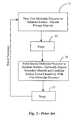
- FIG. 3is a step diagram illustrating steps in a radical-assisted CVD process according to an embodiment of the present invention.
- the inventorhas developed an enhanced variation of ALD which alters the conventional surface preparation steps of ALD and overcomes the problems of conventional ALD, producing high throughput without compromising quality.
- the inventor termsthe new and unique process Radical-Assisted Sequential CVD (FAS-CVD).
- FIG. 1is a generalized diagram of a system 11 for practicing RAS-CVD according to an embodiment of the present invention.
- a deposition chamber 13has a heatable hearth for supporting and heating a substrate 19 to be coated, and a gas distribution apparatus, such as a showerhead 15 , for delivering gaseous species to the substrate surface to be coated.
- Substratesare introduced and removed from chamber 13 via a valve 21 and substrate-handling apparatus not shown.
- Gasesare supplied from a gas sourcing and pulsing apparatus 23 , which includes metering and valving apparatus for sequentially providing gaseous materials.
- An optional treatment apparatus 25is provided for producing gas radicals from gases supplied from apparatus 23 .
- radicalsare well-known and understood in the art, but will be qualified again here to avoid confusion.
- a radicalis meant an unstable species.
- oxygenis stable in diatomic form, and exists principally in nature in this form.
- Diatomic oxygenmay, however, be caused to split to monatomic form, or to combine with another atom to produce ozone, a molecule with three atoms.
- Both monatomic oxygen and ozoneare radical forms of oxygen, and are more reactive than diatomic oxygen.
- the radicals produced and usedare single atom forms of various gases, such as oxygen, hydrogen, and nitrogen, although the invention is not strictly limited to monatomic gases.
- FIG. 2is a step diagram of a conventional Atomic Layer Deposition process, and is presented here as contrast and context for the present invention.
- a first molecular precursoris pulsed in to a reactor chamber, and reacts with the surface to produce (theoretically) a monolayer of a desired material.
- the precursoris a metal-bearing gas, and the material deposited is the metal; Tantalum from TaCl 5 , for example.
- step 33 in the conventional processan inert gas is pulsed into the reactor chamber to sweep excess first precursor from the chamber.
- a second precursortypically non-metallic
- the primary purpose of this second precursoris to condition the substrate surface back toward reactivity with the first precursor.
- the second precursoralso provides material from the molecular gas to combine with metal at the surface, forming compounds such as an oxide or a nitride with the freshly-deposited metal.
- step 37the reactor chamber is purged again to remove excess of the second precursor, and then step 31 is repeated The cycle is repeated as many times as is necessary to establish a desired film.
- FIG. 3is a step diagram illustrating steps in a radical-assisted CVD process according to an embodiment of the present invention.
- the first steps, steps 41 and 43are the same as in the conventional process.
- a first precursoris pulsed in step 41 to react with the substrate surface forming a monolayer of deposit, and the chamber is purges in step 43 .
- the next stepis unique.
- single or multiple radical speciesare pulsed to the substrate surface to optionally provide second material to the surface and to condition the surface toward reactivity with the first molecular precursor in a subsequent step.
- step 41is repeated. There is no need for a second purge, and the cycle is repeated as often as necessary to accomplish the desired film.
- Step 45may be a single step involving a single radical species.
- the first precursormay deposit a metal, such as in W from WF 6
- the radical species in step 45may be atomic hydrogen.
- the atomic hydrogenvery quickly and effectively neutralizes any remaining F to HF, and terminates the surface with atomic hydrogen, providing reactive surface for the next pulse of WF 6 .
- step 45will be a compound step comprising substeps involving different radical species.
- a good exampleis a sequence of atomic hydrogen followed by atomic oxygen, followed by atomic hydrogen again.
- the first hydrogen stepneutralizes Cl or other remaining ligand, the atomic oxygen provides an oxide of the freshly-deposited metal, and the second atomic hydrogen terminated the surface with (OH) in preparation for the next metal precursor step.
- step 45There are a broad variety of materials and combinations in step 45 , and many are disclosed in more detail below, along with a more complete explanation of process chemistry.
- Radical speciesare reactive atoms or molecular fragments that are chemically unstable and therefore are extremely reactive.
- radicalschemisorb to surfaces with virtually 100% efficiency. Radicals may be created in a number of ways, and plasma generation has been found to be an efficient and compatible means of preparation.
- RAS-CVD processesuse only a single molecular precursor, in many cases a metal precursor.
- Surface preparation as well as the deposition of nonmetallic elementsare accomplished by atom-surface reactions.
- the —ML terminated surfaceis reacted with hydrogen atoms to convert the surface into —MH and eliminate HL by-product.
- atom-surface reactionsdo not depend on the number density of reactive sites. Most atoms (except for noble gases) stick very efficiently to surfaces in an irreversible process because atomic desorption is usually unfavorable.
- the atomsare highly mobile on non-reactive sites and very reactive at reactive sites. Consequently, atom-surface reactions have linear exposure dependence, as well as high rates.
- the —MH surfacecan be reacted with A atoms to yield a —M—A— surface.
- some of the H ligandscan be eliminated as AH y .
- the —MH surfacecan be reacted with oxygen atoms to deposit oxide compound.
- —MH surfacecan be reacted again with ML x for atomic layer controlled deposition of M metal films.
- Ais atomic nitrogen.
- the surface after the A atomic reactionis terminated with A— and AH. At this point an additional atomic reaction with hydrogen converts the surface to the desired AH ligands that are reactive towards the metal precursor.
- the MH surfacecan be reacted with a mixture of A and H atoms to convert the surface into —AH terminated surface with one less step. All the above described reactions are radical-surface reactions that are fast and efficient and depend linearly on exposure. In addition, the final hydrogen reaction results in a complete restoration to the initial surface without any incorporation of impurities.
- RAS-CVDAnother throughput benefit of RAS-CVD is that a single purge step after the metal precursor step is needed, rather than the two purge steps needed in the conventional process. Purge steps are expected by most researchers to be the most significant throughput-limiting step in ALD processes. Another advantage is that RAS-CVD promises longer system uptime and reduced maintenance. This is because atomic species can be efficiently quenched on aluminum walls of the deposition module. Downstream deposition on the chamber and pumping lines is therefore virtually eliminated. RAS-CVD eliminates the use of H 2 O and NH 3 that are commonly applied for oxides and nitrides deposition (respectively) in the prior art. These precursors are notorious to increase maintenance and downtime of vacuum systems.
- Atomic hydrogen stepevaporates the ligands L by HL desorption and terminates the surface with hydrogen.
- Atomic oxygen stepreacts with monolayer of metal to form oxide. Atomic hydrogen again to leave hydroxyl saturated surface for next metal precursor step.
- Al 2 O 3 RAS-CVDcan be realized from trimethylaluminum Al(CH 3 ) 3 , hydrogen and oxygen exposures.
- Al(CH 3 ) 3 reacting with —OH terminated surfacewill deposit —OAl(CH 3 ) x concurrent with the desorption of methane (CH 4 ).
- This surface after consecutive (or concurrent) reaction with 0 atoms and H atomswill be terminated —OAl—OH which is the restoration state.
- the RAS-CVD processcan proceed by applying another Al(CH 3 ) 3 reaction.
- the —OAl—OH surfacecan be exposed to another cycles of 0 and H atoms.
- this processwill exchange OH groups and Al—O—Al bridge sites and the resulted —OAl—OH surface will be more thermodynamically favorable than the beginning surface, because the process eliminates the more strained (Al—O—) n ring structures as well as titrating away defects and broken bonds).
- atomic nitrogenis substituted for oxygen.
- oxygen/nitrogen stepmay be eliminated in favor of a single atomic hydrogen step, such as for tungsten films.
- the hydrogen saturated surface after the first atomic hydrogen stepis reactive with WF 6 to produce the pure metal.
- RAS-CVDis advantageous for multiple layer combination films of different oxides, different nitrides, oxides with nitrides, different metals and metals with compound films.
- the WN processmay be combined with the pure W process to produce alternating W and WN layers in a variety of schemes to suppress polycrystallization and to reduce the resistivity of the barrier layer.
- Other properties, such as electromigrationmay be controlled by an ability to provide a graded layer of WN with reduced nitrogen content at the copper interface for such applications.
- Titanium from titanium tetrachloride or titanium tetraiodideis titanium tetrachloride or titanium tetraiodide.
- Titanium oxidefrom titanium tetrachloride or titanium tetraiodide.
- RAS-CVDis compatible in most cases with ALD process hardware.
- the significant differenceis in production of atomic species and/or other radicals, and in the timing and sequence of gases to the process chamber.
- Production of the atomic speciescan be done in several ways, such as (1) in-situ plasma generation, (2) intra-showerhead plasma generation, and (3) external generation by a highdensity remote plasma source or by other means such as UV dissociation or dissociation of metastable molecules referring again to FIG. 1, these methods and apparatus are collectively represented by apparatus 25 .
- Intra-showerhead generationhas been shown to have an advantage of separating the atomic specie generation from the ALD space.
- the preferable method at the time of this specificationis remote generation by a high-density source, as this is the most versatile method.
- the radicalsare generated in a remote source and delivered to the ALD volume, distributed by a showerhead over the wafer in process.
- radicals of the needed speciessuch as hydrogen, oxygen, nitrogen
- ALD chambers, gas distribution, valving, timing and the likemay vary in many particulars.
- metals, oxides nitrides and the likemay be produced, and process steps may be altered and interleaved to create graded and alternating films.
Landscapes
- Chemical & Material Sciences (AREA)
- Engineering & Computer Science (AREA)
- Chemical Kinetics & Catalysis (AREA)
- Physics & Mathematics (AREA)
- General Chemical & Material Sciences (AREA)
- Microelectronics & Electronic Packaging (AREA)
- Condensed Matter Physics & Semiconductors (AREA)
- Power Engineering (AREA)
- Computer Hardware Design (AREA)
- Manufacturing & Machinery (AREA)
- General Physics & Mathematics (AREA)
- Organic Chemistry (AREA)
- Metallurgy (AREA)
- Mechanical Engineering (AREA)
- Materials Engineering (AREA)
- Plasma & Fusion (AREA)
- Electromagnetism (AREA)
- Chemical Vapour Deposition (AREA)
- Vending Machines For Individual Products (AREA)
- Saccharide Compounds (AREA)
- Electrodes Of Semiconductors (AREA)
- Crystals, And After-Treatments Of Crystals (AREA)
- Investigating Or Analysing Materials By The Use Of Chemical Reactions (AREA)
Abstract
Description
- The present invention is in the area of chemical vapor deposition, and pertains more particularly to new methods and apparatus for depositing films by atomic layer deposition.[0001]
- In the manufacture of integrated circuits, deposition of thin films of many pure and compound materials is necessary, and many techniques have been developed to accomplish such depositions. In recent years the dominant technique for deposition of thin films in the art has been chemical vapor deposition (CVD), which has proven to have superior ability to provide uniform even coatings, and to coat relatively conformably into vias and over other high-aspect and uneven features in wafer topology. As device density has continued to increase and geometry has continued to become more complicated, even the superior conformal coating of CVD techniques has been challenged, and new and better techniques are needed.[0002]
- The approach of a variant of CVD, Atomic Layer Deposition has been considered for improvement in uniformity and conformality, especially for low temperature deposition. However the practical implementation of this technology requires a solution to higher purity and higher throughput. This patent addresses these requirements.[0003]
- Atomic Layer Deposition[0004]
- In the field of CVD a process known as Atomic Layer Deposition (ALD) has emerged as a promising candidate to extend the abilities of CVD techniques, and is under rapid development by semiconductor equipment manufacturers to further improve characteristics of chemical vapor deposition. ALD is a process originally termed Atomic Layer Epitaxy, for which a competent reference is:[0005]Atomic Layer Epitaxy,edited by T. Suntola and M. Simpson, published by Blackie, Glasgo and London in 1990. This publication is incorporated herein by reference.
- Generally ALD is a process wherein conventional CVD processes are divided into single-monolayer deposition steps, wherein each separate deposition step theoretically goes to saturation at a single molecular or atomic monolayer thickness, and self-terminates.[0006]
- The deposition is the outcome of chemical reactions between reactive molecular precursors and the substrate. In similarity to CVD, elements composing the film are delivered as molecular precursors. The net reaction must deposit the pure desired film and eliminate the “extra” atoms that compose the molecular precursors (ligands). In the case of CVD the molecular precursors are fed simultaneously into the CVD reactor. A substrate is kept at temperature that is optimized to promote chemical reaction between the molecular precursors concurrent with efficient desorption of byproducts. Accordingly, the reaction proceeds to deposit the desired pure film.[0007]
- For ALD applications, the molecular precursors are introduced into the ALD reactor separately. This is practically done by flowing one precursor at a time, i.e. a metal precursor—ML[0008]x(M═Al, W, Ta, Si etc.) that contains a metal element—M which is bonded to atomic or molecular ligands—L to make a volatile molecule. The metal precursor reaction is typically followed by inert gas purging to eliminate this precursor from the chamber prior to the separate introduction of the other precursor. An ALD reaction will take place only if the surface is prepared to react directly with the molecular precursor. Accordingly the surface is typically prepared to include hydrogen-containing ligands—AH that are reactive with the metal precursor. Surface—molecule reactions can proceed to react with all the ligands on the surface and deposit a monolayer of the metal with its passivating ligand: substrate—AH+MLx→substrate—AMLy+HL, where HL is the exchange reaction by-product. During the reaction the initial surface ligands—AH are consumed and the surface becomes covered with L ligands, that cannot further react with the metal precursor—MLx. Therefore, the reaction self-saturates when all the initial ligands are replaced with—MLyspecies.
- After completing the metal precursor reaction the excess precursor is typically removed from the reactor prior to the introduction of another precursor. The second type of precursor is used to restore the surface reactivity towards the metal precursor, i.e. eliminating the L ligands and redepositing AH ligands.[0009]
- Most ALD processes have been applied to deposit compound films. In this case the second precursor is composed of a desired (usually nonmetallic) element—A (i.e. O, N, S), and hydrogen using, for example H[0010]2O, NH3, or H2S. The reaction: —ML+AHz→—M—AH+HL (for the sake of simplicity the chemical reactions are not balanced) converts the surface back to be AH-covered. The desired additional element—A is deposited and the ligands L are eliminated as volatile by-product. Again, the reaction consumes the reactive sites (this time the L terminated sites) and self-saturates when the reactive sites are entirely depleted.
- The sequence of surface reactions that restores the surface to the initial point is called the ALD deposition cycle. Restoration to the initial surface is the keystone of ALD. It implies that films can be layered down in equal metered sequences that are all identical in chemical kinetics, deposition per cycle, composition and thickness. Self-saturating surface reactions make ALD insensitive to transport nonuniformity either from flow engineering or surface topography (i.e. deposition into high aspect ratio structures). Non uniform flux can only result in different completion time at different areas. However, if each of the reactions is allowed to complete on the entire area, the different completion kinetics bear no penalty.[0011]
- As is often the case with process development, the initial promised advantages of a new technique do not, in the end, attain their full initial promise. Unfortunately, ALD has a serious fundamental problem. Unlike CVD reactions that are of a continuous steady state nature, ALD reactions follow kinetics of molecular-surface interaction. Kinetics of molecular-surface reactions depends on the individual reaction rate between a molecular precursor and a surface reactive site and the number of available reactive sites. As the reaction proceeds to completion, the surface is converted from being reactive to non-reactive. As a result the reaction rate is slowing down during the deposition. In the simplest case the rate, dN/dt is proportional to the number of reactive sites, dN/dt=—kN, where N is the number of reactive sites and k is the (single site) reaction rate. Eliminating reactive sites (or growing of the already-reacted sites) follows an exponential time dependence kN(t)=kN[0012]0exp(—kt). This fundamental property of molecule-surface kinetics was named after the great scientist Langmuir, and is quite well-known in the art.
- The interpretation of Langmuirian kinetics limitations illustrates a serious drawback of ALD and a severe deviation from the ideal picture. Accordingly, the self-terminating reactions never really self-terminate (they would require an infinite time because the rate is exponentially decreasing). It means that under practical conditions the surface is never entirely reacted to completion after a deposition cycle. If the surface is not completely reacted there are leftover undesired elements in the film. For example, if the ML[0013]xreaction cannot totally consume the surface—AH sites, the film will have H incorporation. Likewise, if the AHyreaction is not carried to completion, undesired L incorporation is inevitable. Clearly, the quality of the film depends on the impurity levels. The throughput-quality tradeoff is of particular concern because it carries an exponential throughput penalty to attain a reduction of impurity levels.
- In conventional atomic layer deposition one must accept low throughput to attain high-purity film, or accept lower-purity films for higher throughput. What is clearly needed is an apparatus and methods which not only overcome the Langmuirian limitations but simultaneously provide higher-purity films than have been available in the prior art methods. Such apparatus and methods are provided in embodiments of the present invention, taught in enabling detail below.[0014]
- In a preferred embodiment of the present invention a method for depositing a metal on a substrate surface in a deposition chamber is provided, comprising steps of (a) depositing a monolayer of metal on the substrate surface by flowing a molecular precursor gas or vapor bearing the metal over a surface of the substrate, the surface saturated by a first reactive species with which the precursor will react by depositing the metal and forming reaction product, leaving a metal surface covered with ligands from the metal precursor and therefore not further reactive with the precursor; (b) terminating flow of the precursor gas or vapor; (c) purging the precursor with inert gas; (d) flowing at least one radical species into the chamber and over the surface, the radical species highly reactive with the surface ligands of the metal precursor layer and eliminating the ligands as reaction product, and also saturating the surface, providing the first reactive species; and (e) repeating the steps in order until a metallic film of desired thickness results.[0015]
- In many such embodiments the radical species is atomic hydrogen. Using atomic hydrogen a broad variety of pure metals may be deposited, such as tungsten, tantalum, aluminum, titanium, molybdenum, zinc, hafnium, niobium and copper.[0016]
- In another aspect of the invention a method is provided for depositing a metal oxide on a substrate surface in a deposition chamber, comprising steps of (a) depositing a monolayer of metal on the substrate surface by flowing a metal molecular precursor gas or vapor bearing the metal over a surface of the substrate, the surface saturated by a first reactive species with which the precursor will react by depositing the metal and forming reaction product, leaving a metal surface covered with ligands from the metal precursor and therefore not further reactive with the precursor; (b) terminating flow of the precursor gas or vapor; (c) purging the precursor with inert gas; (d) flowing a first radical species into the chamber and over the surface, the radical species highly reactive with the reaction product and combining with the reaction product to create volatile species and saturate the surface with the first radical species; (e) flowing radical oxygen into the chamber to combine with the metal monolayer deposited in step (a), forming an oxide of the metal; (f) flowing a third radical species into the chamber terminating the surface with the first reactive species in preparation for a next metal deposition step; and (g) repeating the steps in order until a composite film of desired thickness results.[0017]
- In this method the first and third radical species may be both atomic hydrogen, and the metal surface in step (f) is terminated with hydroxyl species reactive with the metal precursor to deposit the metal. In another embodiment the oxygen and hydrogen atomic steps (e) and (f) are repeated to improve film quality. In still another embodiment steps (e) and (f) are combined into one step wherein the surface is reacted with hydrogen and oxygen atoms simultaneously.[0018]
- In various embodiments for depositing oxides the oxides can be tantalum pentoxide, aluminum oxide, titanium oxide, niobium pentoxide, zirconium oxide, hafnium oxide, zinc oxide, molybdenum oxide, manganese oxide, tin oxide, indium oxide, tungsten oxide and silicon oxide, among others.[0019]
- In some embodiments the first radical species is atomic hydrogen and steps (e) and (f) are united to one step using OH radicals, and the metal surface in step (f) is terminated with hydroxyl species reactive with the metal precursor to deposit the metal.[0020]
- In still another aspect of the invention a method for depositing a metal nitride on a substrate surface in a deposition chamber is provided, comprising steps of (a) depositing a monolayer of metal on the substrate surface by flowing a metal precursor gas or vapor bearing the metal over a surface of the substrate, the surface saturated by a first reactive species with which the precursor will react by depositing the metal and forming reaction product, leaving a metal surface covered with ligands from the metal precursor and therefore not further reactive with the precursor, (b) terminating flow of the precursor gas or vapor; (c) purging the precursor with inert gas; (d) flowing a first radical species into the chamber and over the surface, the atomic species highly reactive with the surface ligands of the metal precursor layer and eliminating the ligands as reaction product and also saturating the surface; (e) flowing radical nitrogen into the chamber to combine with the metal monolayer deposited in step (a), forming a nitride of the metal; (f) flowing a third radical species into the chamber terminating the surface with the first reactive species in preparation for a next metal deposition step; and (g) repeating the steps in order until a composite film of desired thickness results.[0021]
- In this method the first and third atomic radical species may both be atomic hydrogen, and the metal surface in step (f) may be terminated with amine species reactive with the metal precursor to deposit the metal. Further, steps (e) and (f) may be combined into one step wherein the surface is reacted with hydrogen and nitrogen atoms simultaneously.[0022]
- In variations of this embodiment a variety of different nitrides may be produces, including, but limited to tungsten nitride, tantalum nitride, aluminum nitride, titanium nitride, silicon nitride and gallium nitride.[0023]
- In another variation the first radical species may be atomic hydrogen and steps (e) and (f) may be united into one step using one or both of NH and NH[0024]2radicals, and the metal surface in step (fi is terminated with amine species reactive with the metal precursor to deposit the metal.
- In yet another aspect of the invention a process for building a metal, metal oxide, or metal nitride film on a substrate surface is provided, wherein deposition steps comprise flowing a metal precursor gas or vapor over the surface with the surface terminated with a first chemical species reactive with the metal precursor to deposit the metal, are alternated with steps comprising flowing radical species over the freshly deposited metal layers to remove the ligands from the deposition steps and to provide the first chemical species to terminate the substrate surface preparatory to the next deposition reaction.[0025]
- In this process a metal nitride film is built up by a step sequence of metal deposition by reacting a metal precursor gas with a surface terminated by amine species, then alternating exposure of the surface with atomic radical hydrogen, nitrogen and hydrogen again, thereby volatilizing products remaining from the metal deposition chemistry, nitridizing the deposited metal monolayer, then terminating the metal surface with amine species again in preparation for a next metal deposition step. A metal oxide film is built up by a step sequence of metal deposition by reacting a metal precursor gas with a surface terminated by hydroxyl species, then alternating exposure of the surface with atomic radical hydrogen, oxygen and hydrogen again, thereby volatilizing products remaining from the metal deposition chemistry, oxidizing the metal monolayer, then terminating the metal surface with hydroxyl species again in preparation for a next metal deposition step.[0026]
- In yet another aspect of the invention a method for depositing a compound film on a substrate surface in a deposition chamber is provided, comprising steps of (a) depositing a monolayer of metal on the substrate surface by flowing a metal molecular precursor gas or vapor bearing the metal over a surface of the substrate, the surface saturated by a first reactive species with which the precursor will react by depositing the metal and forming reaction product, leaving a metal surface covered with ligands from the metal precursor and therefore not further reactive with the precursor; (b) terminating flow of the precursor gas or vapor; (c) purging the precursor with inert gas; (d) flowing a first radical species into the chamber and over the surface, the radical species highly reactive with the reaction product and combining with the reaction product to create volatile species and saturate the surface with the first radical species; (e) flowing nonmetal atomic species into the chamber to combine with the metal monolayer deposited in step (a), forming a compound film of the metal, (f) flowing a third radical species into the chamber terminating the surface with the first reactive species in preparation for a next metal deposition step; and (g) repeating the steps in order until a composite film of desired thickness results.[0027]
- In this method the first and third radical species may be both atomic hydrogen, and the metal surface in step (f) is terminated with hydride species of the nonmetallic element that are reactive with the metal precursor to deposit the metal. In a variation the non-metallic and hydrogen atomic steps (e) and (f) are repeated to improve the film quality. In another variation steps (e) and (f) are combined into one step wherein the surface is reacted with hydrogen and non-metallic atoms simultaneously. A variety of films may be produced by practicing this variation of the invention as well, including but not limited to molybdenum disulfide and zinc sulfide.[0028]
- In yet another aspect of the invention a radical-assisted sequential CVD (RAS-CVD) reactor is provided, comprising a chamber with controlled gas inlets for introducing gases in sequential steps and a heated substrate support for holding a substrate and exposing a surface of the substrate to incoming gases; and a plasma generation apparatus for generating radical atomic species for use in the reactor. In this reactor an aggregate metal layer is formed by depositing a monolayer of metal on the substrate surface by flowing a precursor gas or vapor bearing the metal over a surface of the substrate, the surface terminated by a first reactive species with which the precursor will react by depositing the metal and forming reaction product, leaving a metal surface not further reactive with the precursor, terminating flow of the precursor gas or vapor, flowing at least one atomic radical species into the chamber and over the surface, the atomic species highly reactive with the reaction product and combining with the reaction product, and also terminating the surface, providing the first reactive species, and repeating the steps in order until a composite film of desired thickness results.[0029]
- In various embodiments the atomic radical species is atomic hydrogen. The precursor gas bearing the metal may be tungsten hexafluoride and the metal deposited tungsten.[0030]
- In some embodiments the plasma generation apparatus comprises an electrode within the reactor chamber and a high frequency power supply connected to the electrode. In other embodiments the plasma generation apparatus comprises a showerhead-type gas distribution apparatus, and a plasma is generated within the showerhead apparatus to produce the radical species. In still other embodiments the atomic radical species is produced in a remote plasma generator, and the species are delivered to the reactor.[0031]
- In the various embodiments of the invention a new process is provided wherein films of many sorts, including pure metals, oxides of metals, nitrides of metals, and other films, may be produced quickly and efficiently, with very high purity and with superior conformity to substrate topography and coverage within vias and other difficult surface geometries.[0032]
- FIG. 1 is a generalized diagram of a reactor and associated apparatus for practicing a radical-assisted sequential CVD process according to an embodiment of the present invention.[0033]
- FIG. 2 is a step diagram illustrating the essential steps of an atomic layer deposition process.[0034]
- FIG. 3 is a step diagram illustrating steps in a radical-assisted CVD process according to an embodiment of the present invention.[0035]
- The inventor has developed an enhanced variation of ALD which alters the conventional surface preparation steps of ALD and overcomes the problems of conventional ALD, producing high throughput without compromising quality. The inventor terms the new and unique process Radical-Assisted Sequential CVD (FAS-CVD).[0036]
- FIG. 1 is a generalized diagram of a[0037]
system 11 for practicing RAS-CVD according to an embodiment of the present invention. In this exemplary system adeposition chamber 13 has a heatable hearth for supporting and heating asubstrate 19 to be coated, and a gas distribution apparatus, such as ashowerhead 15, for delivering gaseous species to the substrate surface to be coated. Substrates are introduced and removed fromchamber 13 via avalve 21 and substrate-handling apparatus not shown. Gases are supplied from a gas sourcing andpulsing apparatus 23, which includes metering and valving apparatus for sequentially providing gaseous materials. Anoptional treatment apparatus 25 is provided for producing gas radicals from gases supplied fromapparatus 23. - The term radicals is well-known and understood in the art, but will be qualified again here to avoid confusion. By a radical is meant an unstable species. For example, oxygen is stable in diatomic form, and exists principally in nature in this form. Diatomic oxygen may, however, be caused to split to monatomic form, or to combine with another atom to produce ozone, a molecule with three atoms. Both monatomic oxygen and ozone are radical forms of oxygen, and are more reactive than diatomic oxygen. In many cases in embodiments of the present invention the radicals produced and used are single atom forms of various gases, such as oxygen, hydrogen, and nitrogen, although the invention is not strictly limited to monatomic gases.[0038]
- FIG. 2 is a step diagram of a conventional Atomic Layer Deposition process, and is presented here as contrast and context for the present invention. In conventional ALD, as shown in FIG. 2, in step[0039]31 a first molecular precursor is pulsed in to a reactor chamber, and reacts with the surface to produce (theoretically) a monolayer of a desired material. Often in these processes the precursor is a metal-bearing gas, and the material deposited is the metal; Tantalum from TaCl5, for example.
- In[0040]
step 33 in the conventional process an inert gas is pulsed into the reactor chamber to sweep excess first precursor from the chamber. - In[0041]
step 35 in the conventional system a second precursor, typically non-metallic, is pulsed into the reactor. The primary purpose of this second precursor is to condition the substrate surface back toward reactivity with the first precursor. In many cases the second precursor also provides material from the molecular gas to combine with metal at the surface, forming compounds such as an oxide or a nitride with the freshly-deposited metal. - At[0042]
step 37 the reactor chamber is purged again to remove excess of the second precursor, and then step31 is repeated The cycle is repeated as many times as is necessary to establish a desired film. - FIG. 3 is a step diagram illustrating steps in a radical-assisted CVD process according to an embodiment of the present invention. In the unique process illustrated by FIG. 3 the first steps, steps[0043]41 and43, are the same as in the conventional process. A first precursor is pulsed in
step 41 to react with the substrate surface forming a monolayer of deposit, and the chamber is purges instep 43. The next step is unique. Instep 45 single or multiple radical species are pulsed to the substrate surface to optionally provide second material to the surface and to condition the surface toward reactivity with the first molecular precursor in a subsequent step. Then step41 is repeated. There is no need for a second purge, and the cycle is repeated as often as necessary to accomplish the desired film. - [0044]
Step 45 may be a single step involving a single radical species. For example, the first precursor may deposit a metal, such as in W from WF6, and the radical species instep 45 may be atomic hydrogen. The atomic hydrogen very quickly and effectively neutralizes any remaining F to HF, and terminates the surface with atomic hydrogen, providing reactive surface for the next pulse of WF6. - In many cases step[0045]45 will be a compound step comprising substeps involving different radical species. A good example is a sequence of atomic hydrogen followed by atomic oxygen, followed by atomic hydrogen again. The first hydrogen step neutralizes Cl or other remaining ligand, the atomic oxygen provides an oxide of the freshly-deposited metal, and the second atomic hydrogen terminated the surface with (OH) in preparation for the next metal precursor step.
- There are a broad variety of materials and combinations in[0046]
step 45, and many are disclosed in more detail below, along with a more complete explanation of process chemistry. - In RAS-CVD, following the metal precursor reaction, highly reactive radical species are introduced to quickly react with products of the metal precursor reaction and to prepare the surface for the next metal precursor reaction. Radical species, as introduced above, are reactive atoms or molecular fragments that are chemically unstable and therefore are extremely reactive. In addition, radicals chemisorb to surfaces with virtually 100% efficiency. Radicals may be created in a number of ways, and plasma generation has been found to be an efficient and compatible means of preparation.[0047]
- RAS-CVD processes use only a single molecular precursor, in many cases a metal precursor. Surface preparation as well as the deposition of nonmetallic elements are accomplished by atom-surface reactions. Following the metal precursor reaction, The —ML terminated surface is reacted with hydrogen atoms to convert the surface into —MH and eliminate HL by-product. Unlike molecule-surface reactions, atom-surface reactions do not depend on the number density of reactive sites. Most atoms (except for noble gases) stick very efficiently to surfaces in an irreversible process because atomic desorption is usually unfavorable. The atoms are highly mobile on non-reactive sites and very reactive at reactive sites. Consequently, atom-surface reactions have linear exposure dependence, as well as high rates.[0048]
- The —MH surface can be reacted with A atoms to yield a —M—A— surface. In this case some of the H ligands can be eliminated as AH[0049]y. For example the —MH surface can be reacted with oxygen atoms to deposit oxide compound. Alternatively, —MH surface can be reacted again with MLxfor atomic layer controlled deposition of M metal films. For the deposition of nitride compound films, A is atomic nitrogen. The surface after the A atomic reaction is terminated with A— and AH. At this point an additional atomic reaction with hydrogen converts the surface to the desired AH ligands that are reactive towards the metal precursor. Alternatively, the MH surface can be reacted with a mixture of A and H atoms to convert the surface into —AH terminated surface with one less step. All the above described reactions are radical-surface reactions that are fast and efficient and depend linearly on exposure. In addition, the final hydrogen reaction results in a complete restoration to the initial surface without any incorporation of impurities.
- Another throughput benefit of RAS-CVD is that a single purge step after the metal precursor step is needed, rather than the two purge steps needed in the conventional process. Purge steps are expected by most researchers to be the most significant throughput-limiting step in ALD processes. Another advantage is that RAS-CVD promises longer system uptime and reduced maintenance. This is because atomic species can be efficiently quenched on aluminum walls of the deposition module. Downstream deposition on the chamber and pumping lines is therefore virtually eliminated. RAS-CVD eliminates the use of H[0050]2O and NH3that are commonly applied for oxides and nitrides deposition (respectively) in the prior art. These precursors are notorious to increase maintenance and downtime of vacuum systems.
- According to the above a typical RAS-CVD cycle for a metal oxide film will comprise steps as follows:[0051]
- 1. Metal precursor reaction with —OH (hydroxyl) terminated surface to attach —O—ML[0052]yand eliminate the hydrogen by HL desorption. The surface becomes covered with L ligands, i.e. in the case of TaCl5the surface becomes covered with Cl atoms.
- 2. Purge with inert gas to sweep away excess metal precursor.[0053]
- 3. Atomic hydrogen step—eliminates the ligands L by HL desorption and terminates the surface with hydrogen.[0054]
- 4. Atomic oxygen step—reacts with monolayer of metal to form oxide. Atomic hydrogen again to leave hydroxyl saturated surface for next metal precursor step.[0055]
- At this point the quality of oxide films (i.e. insulation properties, dielectric strength, charge trapping) can be improved by running steps 4+5 for multiple times. For example: Al[0056]2O3RAS-CVD can be realized from trimethylaluminum Al(CH3)3, hydrogen and oxygen exposures. Al(CH3)3reacting with —OH terminated surface will deposit —OAl(CH3)xconcurrent with the desorption of methane (CH4). The —OAl(CH3)x(x=1,2) surface will be treated with H atoms to eliminate x number of methane molecules and terminate the surface with —OAlH. This surface after consecutive (or concurrent) reaction with0 atoms and H atoms will be terminated —OAl—OH which is the restoration state. At this point, the RAS-CVD process can proceed by applying another Al(CH3)3reaction. Alternatively, the —OAl—OH surface can be exposed to another cycles of0 and H atoms. At temperature above 100°C. this process will exchange OH groups and Al—O—Al bridge sites and the resulted —OAl—OH surface will be more thermodynamically favorable than the beginning surface, because the process eliminates the more strained (Al—O—)nring structures as well as titrating away defects and broken bonds). Since the atomic reactions are rather fast, these quality improvements are not expected to be a major throughput concern. In fact, ultimate quality may be achieved by applying the O, H cycles for several times. Following, a given number of O, H atomic reactions the sequence will continue with the next Al(CH3)3reaction.
- 6. Repeat steps from 1.[0057]
- For metal nitrides atomic nitrogen is substituted for oxygen. For pure metal depositions the oxygen/nitrogen step may be eliminated in favor of a single atomic hydrogen step, such as for tungsten films. The hydrogen saturated surface after the first atomic hydrogen step is reactive with WF[0058]6to produce the pure metal.
- The generic nature of RAS-CVD is advantageous for multiple layer combination films of different oxides, different nitrides, oxides with nitrides, different metals and metals with compound films.[0059]
- In another unique process, useful for barrier layers, the WN process may be combined with the pure W process to produce alternating W and WN layers in a variety of schemes to suppress polycrystallization and to reduce the resistivity of the barrier layer. Other properties, such as electromigration may be controlled by an ability to provide a graded layer of WN with reduced nitrogen content at the copper interface for such applications.[0060]
- In embodiments of the invention a broad variety of process chemistries may be practiced, providing a broad variety of final films. In the area of pure metals, for example, the following provides a partial, but not limiting list:[0061]
- 1. Tungsten from tungsten hexafluoride.[0062]
- 2. Tantalum from tantalum pentachloride.[0063]
- 3. Aluminum from either aluminum trichloride or trimethylaluminum.[0064]
- 4. Titanium from titanium tetrachloride or titanium tetraiodide.[0065]
- 5. Molybdenum from molybdenum hexafluoride.[0066]
- 6. Zinc from zinc dichloride.[0067]
- 7. Hafnium from hafnium tetrachloride.[0068]
- 8. Niobium from niobium pentachloride.[0069]
- 9. Copper from Cu[0070]3Cl3
- In the area of oxides the following is a partial but not limiting list:[0071]
- 1. Tantalum pentoxide from tantalum pentachloride.[0072]
- 2. Aluminum oxide from trimethylaluminum or aluminum trichloride.[0073]
- 3. Titanium oxide from titanium tetrachloride or titanium tetraiodide.[0074]
- 4. Niobium pentoxide from niobium pentachloride.[0075]
- 5. Zirconium oxide from zirconium tetrachloride.[0076]
- 6. Hafnium oxide from hafnium tetrachloride.[0077]
- 7. Zinc oxide from zinc dichloride.[0078]
- 8. Molybdenum oxide from molybdenum hexafluoride or molybdenum pentachloride.[0079]
- 9. Manganese oxide from manganese dichloride.[0080]
- 10. Tin oxide from tin tetrachloride.[0081]
- 11. Indium oxide from indium trichloride or trimethylindium.[0082]
- 12. Tungsten oxide from tungsten hexafluoride.[0083]
- 13. Silicon dioxide from silicon tetrachloride.[0084]
- In the area of nitrides, the following is a partial but not limiting list:[0085]
- 1. Tungsten nitride from tungsten hexafluoride.[0086]
- 2. Tantalum nitride from tantalum pentachloride.[0087]
- 3. Aluminum nitride from aluminum trichloride or trimethylaluminum.[0088]
- 4. Titanium nitride from titanium tetrachloride.[0089]
- 5. Silicon nitride from silicon tetrachloride or dichlorosilane.[0090]
- 6. Gallium nitride from trimethylgallium.[0091]
- Hardware Requirements[0092]
- Another advantage of RAS-CVD is that it is compatible in most cases with ALD process hardware. The significant difference is in production of atomic species and/or other radicals, and in the timing and sequence of gases to the process chamber. Production of the atomic species can be done in several ways, such as (1) in-situ plasma generation, (2) intra-showerhead plasma generation, and (3) external generation by a highdensity remote plasma source or by other means such as UV dissociation or dissociation of metastable molecules referring again to FIG. 1, these methods and apparatus are collectively represented by[0093]
apparatus 25. - Of the options, in-situ generation is the simplest design, but poses several problems, such as turn on—turn off times that could be a throughput limitation. Intra-showerhead generation has been shown to have an advantage of separating the atomic specie generation from the ALD space. The preferable method at the time of this specification is remote generation by a high-density source, as this is the most versatile method. The radicals are generated in a remote source and delivered to the ALD volume, distributed by a showerhead over the wafer in process.[0094]
- It will be apparent to the skilled artisan that there are a variety of options that may be exercised within the scope of this invention as variations of the embodiments described above some have already been described. For example, radicals of the needed species, such as hydrogen, oxygen, nitrogen, may be generated in several ways and delivered in the process steps. Further, ALD chambers, gas distribution, valving, timing and the like may vary in many particulars. Still further, many metals, oxides nitrides and the like may be produced, and process steps may be altered and interleaved to create graded and alternating films.[0095]
- In addition to these variations it will be apparent to the skilled artisan that one may, by incorporating processes described herein, alternate process steps in a manner that alloys of two, three or more metals may be deposited, compounds may be deposited with two, three or more constituents, and such things as graded films and nano-laminates may be produced as well. These variations are simply variants using particular embodiments of the invention in alternating cycles, typically in-situ. There are many other variations within the spirit and scope of the invention, so the invention is limited only by the claims that follow.[0096]
Claims (54)
1. A method for depositing a metal on a substrate surface in a deposition chamber, comprising steps of:
(a) depositing a monolayer of metal on the substrate surface by flowing a molecular precursor gas or vapor bearing the metal over a surface of the substrate, the surface saturated by a first reactive species with which the precursor will react by depositing the metal and forming reaction product, leaving a metal surface covered with ligands from the metal precursor and therefore not further reactive with the precursor;
(b) terminating flow of the precursor gas or vapor;
(c) purging the precursor with inert gas;
(d) flowing at least one radical species into the chamber and over the surface, the radical species highly reactive with the surface ligands of the metal precursor layer and eliminating the ligands as reaction product, and also saturating the surface, providing the first reactive species; and
(e) repeating the steps in order until a metallic film of desired thickness results.
2. The method of
claim 1
3. The method of
claim 1
4. The method of
claim 1
5. The method of
claim 1
6. The method of
claim 1
7. The method of
claim 1
8. The method of
claim 1
9. The method of
claim 1
10. The method of
claim 1
11. The method of
claim 1
12. A method for depositing a metal oxide on a substrate surface in a deposition chamber, comprising steps of:
(a) depositing a monolayer of metal on the substrate surface by flowing a metal molecular precursor gas or vapor bearing the metal over a surface of the substrate, the surface saturated by a first reactive species with which the precursor will react by depositing the metal and forming reaction product, leaving a metal surface covered with ligands from the metal precursor and therefore not further reactive with the precursor;
(b) terminating flow of the precursor gas or vapor;
(c) purging the precursor with inert gas;
(d) flowing a first radical species into the chamber and over the surface, the radical species highly reactive with the reaction product and combining with the reaction product to create volatile species and saturate the surface with the first radical species;
(e) flowing radical oxygen into the chamber to combine with the metal monolayer deposited in step (a), forming an oxide of the metal;
(f) flowing a third radical species into the chamber terminating the surface with the first reactive species in preparation for a next metal deposition step; and
(g) repeating the steps in order until a composite film of desired thickness results.
13. The method of
claim 12
14. The method of
claim 13
15. The method of
claim 12
16. The method of
claim 12
17. The method of
claim 12
18. The method of
claim 12
19. The method of
claim 12
20. The method of
claim 12
21. The method of
claim 12
22. The method of
claim 12
23. The method of
claim 12
24. The method of
claim 12
25. The method of
claim 12
26. The method of
claim 12
27. The method of
claim 12
28. The method of
claim 12
29. The method of
claim 12
30. A method for depositing a metal nitride on a substrate surface in a deposition chamber, comprising steps of:
(a) depositing a monolayer of metal on the substrate surface by flowing a metal precursor gas or vapor bearing the metal over a surface of the substrate, the surface saturated by a first reactive species with which the precursor will react by depositing the metal and forming reaction product, leaving a metal surface covered with ligands from the metal precursor and therefore not further reactive with the precursor;
(b) terminating flow of the precursor gas or vapor;
(c) purging the precursor with inert gas;
(d) flowing a first radical species into the chamber and over the surface, the atomic species highly reactive with the surface ligands of the metal precursor layer and eliminating the ligands as reaction product and also saturating the surface;
(e) flowing radical nitrogen into the chamber to combine with the metal monolayer deposited in step (a), forming a nitride of the metal;
(f) flowing a third radical species into the chamber terminating the surface with the first reactive species in preparation for a next metal deposition step; and
(g) repeating the steps in order until a composite film of desired thickness results.
31. The method of
claim 30
32. The method of
claim 31
33. The method of
claim 30
34. The method of
claim 30
35. The method of
claim 30
36. The method of
claim 30
37. The method of
claim 30
38. The method of
claim 30
39. The method of
claim 30
40. A process for building a metal, metal oxide, or metal nitride film on a substrate surface, wherein deposition steps comprising flowing a metal precursor gas or vapor over the surface with the surface terminated with a first chemical species reactive with the metal precursor to deposit the metal, are alternated with steps comprising flowing radical species over the freshly deposited metal layers to remove the ligands from the deposition steps and to provide the first chemical species to terminate the substrate surface preparatory to the next deposition reaction.
41. The process of
claim 40
42. The process of
claim 40
43. A method for depositing a compound film on a substrate surface in a deposition chamber, comprising steps of:
(a) depositing a monolayer of metal on the substrate surface by flowing a metal molecular precursor gas or vapor bearing the metal over a surface of the substrate, the surface saturated by a first reactive species with which the precursor will react by depositing the metal and forming reaction product, leaving a metal surface covered with ligands from the metal precursor and therefore not further reactive with the precursor;
(b) terminating flow of the precursor gas or vapor;
(c) purging the precursor with inert gas;
(d) flowing a first radical species into the chamber and over the surface, the radical species highly reactive with the reaction product and combining with the reaction product to create volatile species and saturate the surface with the first radical species;
(e) flowing nonmetal radical species into the chamber to combine with the metal monolayer deposited in step (a), forming a compound film of the metal;
(f) flowing a third radical species into the chamber terminating the surface with the first reactive species in preparation for a next metal deposition step; and
(g) repeating the steps in order until a composite film of desired thickness results.
44. The method of
claim 43
45. The method of
claim 43
46. The method of
claim 43
47. The method of
claim 43
48. The method of
claim 43
49. A radical-assisted sequential CVD reactor, comprising:
a chamber with controlled gas inlets for introducing gases in sequential steps and a heated substrate support for holding a substrate and exposing a surface of the substrate to incoming gases; and
a plasma generation apparatus for generating radical atomic species for use in the reactor;
wherein an aggregate metal layer is formed by depositing a monolayer of metal on the substrate surface by flowing a precursor gas or vapor bearing the metal over a surface of the substrate, the surface terminated by a first reactive species with which the precursor will react by depositing the metal and forming reaction product, leaving a metal surface not further reactive with the precursor, terminating flow of the precursor gas or vapor, flowing at least one atomic radical species into the chamber and over the surface, the atomic species highly reactive with the reaction product and combining with the reaction product, and also terminating the surface, providing the first reactive species, and repeating the steps in order until a composite film of desired thickness results.
50. The reactor of
claim 49
51. The reactor of
claim 49
52. The reactor of
claim 49
53. The reactor of
claim 49
54. The reactor of
claim 49
Priority Applications (4)
| Application Number | Priority Date | Filing Date | Title |
|---|---|---|---|
| US09/747,649US6451695B2 (en) | 1999-03-11 | 2000-12-22 | Radical-assisted sequential CVD |
| US10/213,915US6602784B2 (en) | 1999-03-11 | 2002-08-06 | Radical-assisted sequential CVD |
| US10/213,781US6638862B2 (en) | 1999-03-11 | 2002-08-06 | Radical-assisted sequential CVD |
| US10/213,914US6630401B2 (en) | 1999-03-11 | 2002-08-06 | Radical-assisted sequential CVD |
Applications Claiming Priority (2)
| Application Number | Priority Date | Filing Date | Title |
|---|---|---|---|
| US09/267,953US6200893B1 (en) | 1999-03-11 | 1999-03-11 | Radical-assisted sequential CVD |
| US09/747,649US6451695B2 (en) | 1999-03-11 | 2000-12-22 | Radical-assisted sequential CVD |
Related Parent Applications (1)
| Application Number | Title | Priority Date | Filing Date |
|---|---|---|---|
| US09/267,953DivisionUS6200893B1 (en) | 1999-03-11 | 1999-03-11 | Radical-assisted sequential CVD |
Related Child Applications (4)
| Application Number | Title | Priority Date | Filing Date |
|---|---|---|---|
| US09/267,953DivisionUS6200893B1 (en) | 1999-03-11 | 1999-03-11 | Radical-assisted sequential CVD |
| US10/213,914DivisionUS6630401B2 (en) | 1999-03-11 | 2002-08-06 | Radical-assisted sequential CVD |
| US10/213,915DivisionUS6602784B2 (en) | 1999-03-11 | 2002-08-06 | Radical-assisted sequential CVD |
| US10/213,781DivisionUS6638862B2 (en) | 1999-03-11 | 2002-08-06 | Radical-assisted sequential CVD |
Publications (2)
| Publication Number | Publication Date |
|---|---|
| US20010002280A1true US20010002280A1 (en) | 2001-05-31 |
| US6451695B2 US6451695B2 (en) | 2002-09-17 |
Family
ID=23020817
Family Applications (6)
| Application Number | Title | Priority Date | Filing Date |
|---|---|---|---|
| US09/267,953Expired - LifetimeUS6200893B1 (en) | 1999-03-11 | 1999-03-11 | Radical-assisted sequential CVD |
| US09/669,063Expired - LifetimeUS6475910B1 (en) | 1999-03-11 | 2000-09-22 | Radical-assisted sequential CVD |
| US09/747,649Expired - Fee RelatedUS6451695B2 (en) | 1999-03-11 | 2000-12-22 | Radical-assisted sequential CVD |
| US10/213,781Expired - LifetimeUS6638862B2 (en) | 1999-03-11 | 2002-08-06 | Radical-assisted sequential CVD |
| US10/213,914Expired - LifetimeUS6630401B2 (en) | 1999-03-11 | 2002-08-06 | Radical-assisted sequential CVD |
| US10/213,915Expired - Fee RelatedUS6602784B2 (en) | 1999-03-11 | 2002-08-06 | Radical-assisted sequential CVD |
Family Applications Before (2)
| Application Number | Title | Priority Date | Filing Date |
|---|---|---|---|
| US09/267,953Expired - LifetimeUS6200893B1 (en) | 1999-03-11 | 1999-03-11 | Radical-assisted sequential CVD |
| US09/669,063Expired - LifetimeUS6475910B1 (en) | 1999-03-11 | 2000-09-22 | Radical-assisted sequential CVD |
Family Applications After (3)
| Application Number | Title | Priority Date | Filing Date |
|---|---|---|---|
| US10/213,781Expired - LifetimeUS6638862B2 (en) | 1999-03-11 | 2002-08-06 | Radical-assisted sequential CVD |
| US10/213,914Expired - LifetimeUS6630401B2 (en) | 1999-03-11 | 2002-08-06 | Radical-assisted sequential CVD |
| US10/213,915Expired - Fee RelatedUS6602784B2 (en) | 1999-03-11 | 2002-08-06 | Radical-assisted sequential CVD |
Country Status (8)
| Country | Link |
|---|---|
| US (6) | US6200893B1 (en) |
| EP (1) | EP1125324B1 (en) |
| JP (1) | JP3798248B2 (en) |
| KR (1) | KR100489140B1 (en) |
| AT (1) | ATE323948T1 (en) |
| AU (1) | AU3479100A (en) |
| DE (2) | DE1125324T1 (en) |
| WO (1) | WO2000054320A1 (en) |
Cited By (134)
| Publication number | Priority date | Publication date | Assignee | Title |
|---|---|---|---|---|
| US20020036780A1 (en)* | 2000-09-27 | 2002-03-28 | Hiroaki Nakamura | Image processing apparatus |
| US20020197863A1 (en)* | 2001-06-20 | 2002-12-26 | Mak Alfred W. | System and method to form a composite film stack utilizing sequential deposition techniques |
| US20030013300A1 (en)* | 2001-07-16 | 2003-01-16 | Applied Materials, Inc. | Method and apparatus for depositing tungsten after surface treatment to improve film characteristics |
| US20030045060A1 (en)* | 2001-08-30 | 2003-03-06 | Micron Technology, Inc. | Crystalline or amorphous medium-k gate oxides, Y2O3 and Gd2O3 |
| US20030082307A1 (en)* | 2001-10-26 | 2003-05-01 | Applied Materials, Inc. | Integration of ALD tantalum nitride and alpha-phase tantalum for copper metallization application |
| US20030104126A1 (en)* | 2001-10-10 | 2003-06-05 | Hongbin Fang | Method for depositing refractory metal layers employing sequential deposition techniques |
| US20030108674A1 (en)* | 2001-12-07 | 2003-06-12 | Applied Materials, Inc. | Cyclical deposition of refractory metal silicon nitride |
| US20030106490A1 (en)* | 2001-12-06 | 2003-06-12 | Applied Materials, Inc. | Apparatus and method for fast-cycle atomic layer deposition |
| US20030119246A1 (en)* | 2001-12-20 | 2003-06-26 | Micron Technology, Inc. | Low-temperature grown high quality ultra-thin CoTiO3 gate dielectrics |
| US20030127043A1 (en)* | 2001-07-13 | 2003-07-10 | Applied Materials, Inc. | Pulsed nucleation deposition of tungsten layers |
| US20030153181A1 (en)* | 2002-02-11 | 2003-08-14 | Applied Materials, Inc. | Deposition of tungsten films |
| US20030161952A1 (en)* | 2002-02-26 | 2003-08-28 | Applied Materials, Inc. | Cyclical deposition of tungsten nitride for metal oxide gate electrode |
| US20030186561A1 (en)* | 2002-03-26 | 2003-10-02 | Applied Materials, Inc. | Deposition of film layers |
| US20030190497A1 (en)* | 2002-04-08 | 2003-10-09 | Applied Materials, Inc. | Cyclical deposition of a variable content titanium silicon nitride layer |
| US6638810B2 (en) | 2000-02-22 | 2003-10-28 | Applied Materials, Inc. | Tantalum nitride CVD deposition by tantalum oxide densification |
| US20030224600A1 (en)* | 2002-03-04 | 2003-12-04 | Wei Cao | Sequential deposition of tantalum nitride using a tantalum-containing precursor and a nitrogen-containing precursor |
| US20030224578A1 (en)* | 2001-12-21 | 2003-12-04 | Hua Chung | Selective deposition of a barrier layer on a dielectric material |
| US20030232501A1 (en)* | 2002-06-14 | 2003-12-18 | Kher Shreyas S. | Surface pre-treatment for enhancement of nucleation of high dielectric constant materials |
| US20030232511A1 (en)* | 2002-06-14 | 2003-12-18 | Applied Materials, Inc. | ALD metal oxide deposition process using direct oxidation |
| US20030232497A1 (en)* | 2002-04-16 | 2003-12-18 | Ming Xi | System and method for forming an integrated barrier layer |
| WO2003105205A1 (en)* | 2002-06-05 | 2003-12-18 | Micron Technology, Inc. | Hafnium-aluminum oxide dielectric films |
| US20030235961A1 (en)* | 2002-04-17 | 2003-12-25 | Applied Materials, Inc. | Cyclical sequential deposition of multicomponent films |
| US20040011404A1 (en)* | 2002-07-19 | 2004-01-22 | Ku Vincent W | Valve design and configuration for fast delivery system |
| US20040013803A1 (en)* | 2002-07-16 | 2004-01-22 | Applied Materials, Inc. | Formation of titanium nitride films using a cyclical deposition process |
| WO2004007796A1 (en)* | 2002-07-12 | 2004-01-22 | President And Fellows Of Harvard College | Vapor deposition of tungsten nitride |
| US20040018304A1 (en)* | 2002-07-10 | 2004-01-29 | Applied Materials, Inc. | Method of film deposition using activated precursor gases |
| US20040018723A1 (en)* | 2000-06-27 | 2004-01-29 | Applied Materials, Inc. | Formation of boride barrier layers using chemisorption techniques |
| US20040033681A1 (en)* | 2002-08-15 | 2004-02-19 | Micron Technology, Inc. | Lanthanide doped TiOx dielectric films by plasma oxidation |
| US20040043569A1 (en)* | 2002-08-28 | 2004-03-04 | Ahn Kie Y. | Atomic layer deposited HfSiON dielectric films |
| US20040043541A1 (en)* | 2002-08-29 | 2004-03-04 | Ahn Kie Y. | Atomic layer deposited lanthanide doped TiOx dielectric films |
| US6718126B2 (en) | 2001-09-14 | 2004-04-06 | Applied Materials, Inc. | Apparatus and method for vaporizing solid precursor for CVD or atomic layer deposition |
| US20040067641A1 (en)* | 2002-10-02 | 2004-04-08 | Applied Materials, Inc. | Gas distribution system for cyclical layer deposition |
| US20040071897A1 (en)* | 2002-10-11 | 2004-04-15 | Applied Materials, Inc. | Activated species generator for rapid cycle deposition processes |
| US20040077183A1 (en)* | 2002-06-04 | 2004-04-22 | Hua Chung | Titanium tantalum nitride silicide layer |
| US20040115898A1 (en)* | 2002-12-13 | 2004-06-17 | Applied Materials, Inc. | Deposition process for high aspect ratio trenches |
| US6753248B1 (en) | 2003-01-27 | 2004-06-22 | Applied Materials, Inc. | Post metal barrier/adhesion film |
| US20040144311A1 (en)* | 2002-11-14 | 2004-07-29 | Ling Chen | Apparatus and method for hybrid chemical processing |
| US6772072B2 (en) | 2002-07-22 | 2004-08-03 | Applied Materials, Inc. | Method and apparatus for monitoring solid precursor delivery |
| US20040164365A1 (en)* | 2002-08-15 | 2004-08-26 | Micron Technology, Inc. | Lanthanide doped TiOx dielectric films |
| US20040185654A1 (en)* | 2001-12-20 | 2004-09-23 | Micron Technology, Inc. | Low-temperature growth high-quality ultra-thin praseodymium gate dielectrics |
| US20040197492A1 (en)* | 2001-05-07 | 2004-10-07 | Applied Materials, Inc. | CVD TiSiN barrier for copper integration |
| US20040198069A1 (en)* | 2003-04-04 | 2004-10-07 | Applied Materials, Inc. | Method for hafnium nitride deposition |
| US20040209465A1 (en)* | 2000-06-28 | 2004-10-21 | Applied Materials, Inc. | Method and apparatus for depositing refractory metal layers employing sequential deposition techniques to form a nucleation layer |
| US6809026B2 (en) | 2001-12-21 | 2004-10-26 | Applied Materials, Inc. | Selective deposition of a barrier layer on a metal film |
| US20040222476A1 (en)* | 2002-01-17 | 2004-11-11 | Micron Technology, Inc. | Highly reliable amorphous high-k gate dielectric ZrOxNy |
| US20040256351A1 (en)* | 2003-01-07 | 2004-12-23 | Hua Chung | Integration of ALD/CVD barriers with porous low k materials |
| US20050009325A1 (en)* | 2003-06-18 | 2005-01-13 | Hua Chung | Atomic layer deposition of barrier materials |
| US20050009371A1 (en)* | 2002-06-14 | 2005-01-13 | Metzner Craig R. | System and method for forming a gate dielectric |
| US20050008779A1 (en)* | 2002-04-08 | 2005-01-13 | Yang Michael Xi | Multiple precursor cyclical depositon system |
| US20050020017A1 (en)* | 2003-06-24 | 2005-01-27 | Micron Technology, Inc. | Lanthanide oxide / hafnium oxide dielectric layers |
| US20050019494A1 (en)* | 2003-07-25 | 2005-01-27 | Applied Materials, Inc., A Delaware Corporation | Sequential gas flow oxide deposition technique |
| US6855368B1 (en) | 2000-06-28 | 2005-02-15 | Applied Materials, Inc. | Method and system for controlling the presence of fluorine in refractory metal layers |
| US20050067103A1 (en)* | 2003-09-26 | 2005-03-31 | Applied Materials, Inc. | Interferometer endpoint monitoring device |
| US6893978B1 (en)* | 2002-12-03 | 2005-05-17 | Silicon Magnetic Systems | Method for oxidizing a metal layer |
| US6911391B2 (en) | 2002-01-26 | 2005-06-28 | Applied Materials, Inc. | Integration of titanium and titanium nitride layers |
| US6915592B2 (en) | 2002-07-29 | 2005-07-12 | Applied Materials, Inc. | Method and apparatus for generating gas to a processing chamber |
| US20050164521A1 (en)* | 2002-12-04 | 2005-07-28 | Micron Technology, Inc. | Zr-Sn-Ti-O films |
| US6939804B2 (en) | 2001-07-16 | 2005-09-06 | Applied Materials, Inc. | Formation of composite tungsten films |
| US6955211B2 (en) | 2002-07-17 | 2005-10-18 | Applied Materials, Inc. | Method and apparatus for gas temperature control in a semiconductor processing system |
| US20050280067A1 (en)* | 2003-04-22 | 2005-12-22 | Micron Technology, Inc. | Atomic layer deposited zirconium titanium oxide films |
| US20060019495A1 (en)* | 2004-07-20 | 2006-01-26 | Applied Materials, Inc. | Atomic layer deposition of tantalum-containing materials using the tantalum precursor taimata |
| US6998014B2 (en) | 2002-01-26 | 2006-02-14 | Applied Materials, Inc. | Apparatus and method for plasma assisted deposition |
| US20060062917A1 (en)* | 2004-05-21 | 2006-03-23 | Shankar Muthukrishnan | Vapor deposition of hafnium silicate materials with tris(dimethylamino)silane |
| US7049226B2 (en) | 2001-09-26 | 2006-05-23 | Applied Materials, Inc. | Integration of ALD tantalum nitride for copper metallization |
| US20060128150A1 (en)* | 2004-12-10 | 2006-06-15 | Applied Materials, Inc. | Ruthenium as an underlayer for tungsten film deposition |
| US20060148180A1 (en)* | 2005-01-05 | 2006-07-06 | Micron Technology, Inc. | Atomic layer deposited hafnium tantalum oxide dielectrics |
| US7081421B2 (en) | 2004-08-26 | 2006-07-25 | Micron Technology, Inc. | Lanthanide oxide dielectric layer |
| US7087497B2 (en) | 2004-03-04 | 2006-08-08 | Applied Materials | Low-thermal-budget gapfill process |
| US20060177975A1 (en)* | 2005-02-10 | 2006-08-10 | Micron Technology, Inc. | Atomic layer deposition of CeO2/Al2O3 films as gate dielectrics |
| US7160577B2 (en) | 2002-05-02 | 2007-01-09 | Micron Technology, Inc. | Methods for atomic-layer deposition of aluminum oxides in integrated circuits |
| US20070048977A1 (en)* | 2005-08-24 | 2007-03-01 | Jung-Wook Lee | Method of depositing Ge-Sb-Te thin film |
| US20070049043A1 (en)* | 2005-08-23 | 2007-03-01 | Applied Materials, Inc. | Nitrogen profile engineering in HI-K nitridation for device performance enhancement and reliability improvement |
| US7235501B2 (en) | 2004-12-13 | 2007-06-26 | Micron Technology, Inc. | Lanthanum hafnium oxide dielectrics |
| US7259434B2 (en) | 2001-08-30 | 2007-08-21 | Micron Technology, Inc. | Highly reliable amorphous high-k gate oxide ZrO2 |
| US20070197398A1 (en)* | 2004-03-01 | 2007-08-23 | Yasuhiko Kojima | Copper film deposition method |
| US7262133B2 (en) | 2003-01-07 | 2007-08-28 | Applied Materials, Inc. | Enhancement of copper line reliability using thin ALD tan film to cap the copper line |
| US7352048B2 (en) | 2001-09-26 | 2008-04-01 | Applied Materials, Inc. | Integration of barrier layer and seed layer |
| US20080085611A1 (en)* | 2006-10-09 | 2008-04-10 | Amit Khandelwal | Deposition and densification process for titanium nitride barrier layers |
| US20080099436A1 (en)* | 2006-10-30 | 2008-05-01 | Michael Grimbergen | Endpoint detection for photomask etching |
| US7390756B2 (en) | 2005-04-28 | 2008-06-24 | Micron Technology, Inc. | Atomic layer deposited zirconium silicon oxide films |
| US7402534B2 (en) | 2005-08-26 | 2008-07-22 | Applied Materials, Inc. | Pretreatment processes within a batch ALD reactor |
| US7402876B2 (en) | 2002-12-04 | 2008-07-22 | Micron Technology, Inc. | Zr— Sn—Ti—O films |
| US20080176149A1 (en)* | 2006-10-30 | 2008-07-24 | Applied Materials, Inc. | Endpoint detection for photomask etching |
| US7405158B2 (en) | 2000-06-28 | 2008-07-29 | Applied Materials, Inc. | Methods for depositing tungsten layers employing atomic layer deposition techniques |
| US7405454B2 (en) | 2003-03-04 | 2008-07-29 | Micron Technology, Inc. | Electronic apparatus with deposited dielectric layers |
| US20080182021A1 (en)* | 2007-01-31 | 2008-07-31 | Simka Harsono S | Continuous ultra-thin copper film formed using a low thermal budget |
| US7410668B2 (en) | 2001-03-01 | 2008-08-12 | Micron Technology, Inc. | Methods, systems, and apparatus for uniform chemical-vapor depositions |
| US7416979B2 (en) | 2001-07-25 | 2008-08-26 | Applied Materials, Inc. | Deposition methods for barrier and tungsten materials |
| US7429361B2 (en) | 2002-07-17 | 2008-09-30 | Applied Materials, Inc. | Method and apparatus for providing precursor gas to a processing chamber |
| US7470611B2 (en) | 1998-10-01 | 2008-12-30 | Applied Materials, Inc. | In situ deposition of a low K dielectric layer, barrier layer, etch stop, and anti-reflective coating for damascene application |
| US7494939B2 (en) | 2004-08-31 | 2009-02-24 | Micron Technology, Inc. | Methods for forming a lanthanum-metal oxide dielectric layer |
| US20090081868A1 (en)* | 2007-09-25 | 2009-03-26 | Applied Materials, Inc. | Vapor deposition processes for tantalum carbide nitride materials |
| US20090078916A1 (en)* | 2007-09-25 | 2009-03-26 | Applied Materials, Inc. | Tantalum carbide nitride materials by vapor deposition processes |
| US7511326B2 (en) | 2005-03-29 | 2009-03-31 | Micron Technology, Inc. | ALD of amorphous lanthanide doped TiOx films |
| US20090087585A1 (en)* | 2007-09-28 | 2009-04-02 | Wei Ti Lee | Deposition processes for titanium nitride barrier and aluminum |
| US7560793B2 (en) | 2002-05-02 | 2009-07-14 | Micron Technology, Inc. | Atomic layer deposition and conversion |
| US7572695B2 (en) | 2005-05-27 | 2009-08-11 | Micron Technology, Inc. | Hafnium titanium oxide films |
| US7588988B2 (en) | 2004-08-31 | 2009-09-15 | Micron Technology, Inc. | Method of forming apparatus having oxide films formed using atomic layer deposition |
| US7605030B2 (en) | 2006-08-31 | 2009-10-20 | Micron Technology, Inc. | Hafnium tantalum oxynitride high-k dielectric and metal gates |
| US7611990B2 (en) | 2001-07-25 | 2009-11-03 | Applied Materials, Inc. | Deposition methods for barrier and tungsten materials |
| US7659158B2 (en) | 2008-03-31 | 2010-02-09 | Applied Materials, Inc. | Atomic layer deposition processes for non-volatile memory devices |
| US7662729B2 (en) | 2005-04-28 | 2010-02-16 | Micron Technology, Inc. | Atomic layer deposition of a ruthenium layer to a lanthanide oxide dielectric layer |
| US7682946B2 (en) | 2005-11-04 | 2010-03-23 | Applied Materials, Inc. | Apparatus and process for plasma-enhanced atomic layer deposition |
| US7687409B2 (en) | 2005-03-29 | 2010-03-30 | Micron Technology, Inc. | Atomic layer deposited titanium silicon oxide films |
| US7700155B1 (en)* | 2004-04-08 | 2010-04-20 | Novellus Systems, Inc. | Method and apparatus for modulation of precursor exposure during a pulsed deposition process |
| US7709402B2 (en) | 2006-02-16 | 2010-05-04 | Micron Technology, Inc. | Conductive layers for hafnium silicon oxynitride films |
| US7728626B2 (en) | 2002-07-08 | 2010-06-01 | Micron Technology, Inc. | Memory utilizing oxide nanolaminates |
| US7732327B2 (en) | 2000-06-28 | 2010-06-08 | Applied Materials, Inc. | Vapor deposition of tungsten materials |
| US7780785B2 (en) | 2001-10-26 | 2010-08-24 | Applied Materials, Inc. | Gas delivery apparatus for atomic layer deposition |
| US7794544B2 (en) | 2004-05-12 | 2010-09-14 | Applied Materials, Inc. | Control of gas flow and delivery to suppress the formation of particles in an MOCVD/ALD system |
| US7798096B2 (en) | 2006-05-05 | 2010-09-21 | Applied Materials, Inc. | Plasma, UV and ion/neutral assisted ALD or CVD in a batch tool |
| US20100311237A1 (en)* | 2001-02-02 | 2010-12-09 | Seutter Sean M | Formation of a tantalum-nitride layer |
| US20100323512A1 (en)* | 2009-06-17 | 2010-12-23 | Tokyo Electron Limited | Metal oxide film formation method and apparatus |
| US7964505B2 (en) | 2005-01-19 | 2011-06-21 | Applied Materials, Inc. | Atomic layer deposition of tungsten materials |
| US8110489B2 (en) | 2001-07-25 | 2012-02-07 | Applied Materials, Inc. | Process for forming cobalt-containing materials |
| US8119210B2 (en) | 2004-05-21 | 2012-02-21 | Applied Materials, Inc. | Formation of a silicon oxynitride layer on a high-k dielectric material |
| US8125038B2 (en) | 2002-07-30 | 2012-02-28 | Micron Technology, Inc. | Nanolaminates of hafnium oxide and zirconium oxide |
| US8146896B2 (en) | 2008-10-31 | 2012-04-03 | Applied Materials, Inc. | Chemical precursor ampoule for vapor deposition processes |
| US8187970B2 (en) | 2001-07-25 | 2012-05-29 | Applied Materials, Inc. | Process for forming cobalt and cobalt silicide materials in tungsten contact applications |
| US8323754B2 (en) | 2004-05-21 | 2012-12-04 | Applied Materials, Inc. | Stabilization of high-k dielectric materials |
| US8491967B2 (en) | 2008-09-08 | 2013-07-23 | Applied Materials, Inc. | In-situ chamber treatment and deposition process |
| US8501563B2 (en) | 2005-07-20 | 2013-08-06 | Micron Technology, Inc. | Devices with nanocrystals and methods of formation |
| US20130240478A1 (en)* | 2012-03-14 | 2013-09-19 | Applied Materials, Inc. | METHODS FOR DEPOSITING A TiN-CONTAINING LAYER ON A SUBSTRATE |
| US8778574B2 (en) | 2012-11-30 | 2014-07-15 | Applied Materials, Inc. | Method for etching EUV material layers utilized to form a photomask |
| US8778204B2 (en) | 2010-10-29 | 2014-07-15 | Applied Materials, Inc. | Methods for reducing photoresist interference when monitoring a target layer in a plasma process |
| US8808559B2 (en) | 2011-11-22 | 2014-08-19 | Applied Materials, Inc. | Etch rate detection for reflective multi-material layers etching |
| US8900469B2 (en) | 2011-12-19 | 2014-12-02 | Applied Materials, Inc. | Etch rate detection for anti-reflective coating layer and absorber layer etching |
| US8961804B2 (en) | 2011-10-25 | 2015-02-24 | Applied Materials, Inc. | Etch rate detection for photomask etching |
| US9051641B2 (en) | 2001-07-25 | 2015-06-09 | Applied Materials, Inc. | Cobalt deposition on barrier surfaces |
| US9353439B2 (en) | 2013-04-05 | 2016-05-31 | Lam Research Corporation | Cascade design showerhead for transient uniformity |
| US9418890B2 (en) | 2008-09-08 | 2016-08-16 | Applied Materials, Inc. | Method for tuning a deposition rate during an atomic layer deposition process |
| US9805939B2 (en) | 2012-10-12 | 2017-10-31 | Applied Materials, Inc. | Dual endpoint detection for advanced phase shift and binary photomasks |
| US10023959B2 (en) | 2015-05-26 | 2018-07-17 | Lam Research Corporation | Anti-transient showerhead |
| US11038153B2 (en)* | 2019-01-15 | 2021-06-15 | Applied Materials, Inc. | Methods for HMDSO thermal stability |
Families Citing this family (438)
| Publication number | Priority date | Publication date | Assignee | Title |
|---|---|---|---|---|
| FI119941B (en)* | 1999-10-15 | 2009-05-15 | Asm Int | Process for the preparation of nanolaminates |
| US6342277B1 (en)* | 1996-08-16 | 2002-01-29 | Licensee For Microelectronics: Asm America, Inc. | Sequential chemical vapor deposition |
| US5862223A (en) | 1996-07-24 | 1999-01-19 | Walker Asset Management Limited Partnership | Method and apparatus for a cryptographically-assisted commercial network system designed to facilitate and support expert-based commerce |
| US7393561B2 (en)* | 1997-08-11 | 2008-07-01 | Applied Materials, Inc. | Method and apparatus for layer by layer deposition of thin films |
| US7829144B2 (en)* | 1997-11-05 | 2010-11-09 | Tokyo Electron Limited | Method of forming a metal film for electrode |
| JPH11195621A (en)* | 1997-11-05 | 1999-07-21 | Tokyo Electron Ltd | Barrier metal, method of forming the same, gate electrode and method of forming the same |
| US6861356B2 (en)* | 1997-11-05 | 2005-03-01 | Tokyo Electron Limited | Method of forming a barrier film and method of forming wiring structure and electrodes of semiconductor device having a barrier film |
| US6540838B2 (en) | 2000-11-29 | 2003-04-01 | Genus, Inc. | Apparatus and concept for minimizing parasitic chemical vapor deposition during atomic layer deposition |
| US6200893B1 (en)* | 1999-03-11 | 2001-03-13 | Genus, Inc | Radical-assisted sequential CVD |
| US6958174B1 (en)* | 1999-03-15 | 2005-10-25 | Regents Of The University Of Colorado | Solid material comprising a thin metal film on its surface and methods for producing the same |
| KR100273473B1 (en)* | 1999-04-06 | 2000-11-15 | 이경수 | Method for forming a thin film |
| US8206568B2 (en)* | 1999-06-22 | 2012-06-26 | President And Fellows Of Harvard College | Material deposition techniques for control of solid state aperture surface properties |
| FI110311B (en) | 1999-07-20 | 2002-12-31 | Asm Microchemistry Oy | Method and apparatus for eliminating substances from gases |
| US7554829B2 (en) | 1999-07-30 | 2009-06-30 | Micron Technology, Inc. | Transmission lines for CMOS integrated circuits |
| US6391785B1 (en)* | 1999-08-24 | 2002-05-21 | Interuniversitair Microelektronica Centrum (Imec) | Method for bottomless deposition of barrier layers in integrated circuit metallization schemes |
| US6511539B1 (en)* | 1999-09-08 | 2003-01-28 | Asm America, Inc. | Apparatus and method for growth of a thin film |
| WO2001029893A1 (en)* | 1999-10-15 | 2001-04-26 | Asm America, Inc. | Method for depositing nanolaminate thin films on sensitive surfaces |
| US6727169B1 (en)* | 1999-10-15 | 2004-04-27 | Asm International, N.V. | Method of making conformal lining layers for damascene metallization |
| US6503330B1 (en)* | 1999-12-22 | 2003-01-07 | Genus, Inc. | Apparatus and method to achieve continuous interface and ultrathin film during atomic layer deposition |
| US6524317B1 (en)* | 1999-12-30 | 2003-02-25 | Opus Medical, Inc. | Method and apparatus for attaching connective tissues to bone using a knotless suture anchoring device |
| US6551399B1 (en) | 2000-01-10 | 2003-04-22 | Genus Inc. | Fully integrated process for MIM capacitors using atomic layer deposition |
| US6492283B2 (en) | 2000-02-22 | 2002-12-10 | Asm Microchemistry Oy | Method of forming ultrathin oxide layer |
| JP5016767B2 (en) | 2000-03-07 | 2012-09-05 | エーエスエム インターナショナル エヌ.ヴェー. | Method for forming gradient thin film |
| US7419903B2 (en)* | 2000-03-07 | 2008-09-02 | Asm International N.V. | Thin films |
| FI117978B (en)* | 2000-04-14 | 2007-05-15 | Asm Int | Method and apparatus for constructing a thin film on a substrate |
| US7060132B2 (en)* | 2000-04-14 | 2006-06-13 | Asm International N.V. | Method and apparatus of growing a thin film |
| US6596343B1 (en)* | 2000-04-21 | 2003-07-22 | Applied Materials, Inc. | Method and apparatus for processing semiconductor substrates with hydroxyl radicals |
| EP1292970B1 (en)* | 2000-06-08 | 2011-09-28 | Genitech Inc. | Thin film forming method |
| US20040224504A1 (en)* | 2000-06-23 | 2004-11-11 | Gadgil Prasad N. | Apparatus and method for plasma enhanced monolayer processing |
| KR100332313B1 (en)* | 2000-06-24 | 2002-04-12 | 서성기 | Apparatus and method for depositing thin film on wafer |
| KR100351056B1 (en)* | 2000-06-27 | 2002-09-05 | 삼성전자 주식회사 | Method of manufacturing semiconductor device including step of selectively forming metal oxide layer |
| KR100396694B1 (en)* | 2000-07-27 | 2003-09-02 | 주식회사 하이닉스반도체 | Method for forming thin film using atomic layer deposition |
| US7465478B2 (en)* | 2000-08-11 | 2008-12-16 | Applied Materials, Inc. | Plasma immersion ion implantation process |
| US7288491B2 (en)* | 2000-08-11 | 2007-10-30 | Applied Materials, Inc. | Plasma immersion ion implantation process |
| US20050230047A1 (en)* | 2000-08-11 | 2005-10-20 | Applied Materials, Inc. | Plasma immersion ion implantation apparatus |
| US6585730B1 (en)* | 2000-08-30 | 2003-07-01 | Opus Medical, Inc. | Method and apparatus for attaching connective tissues to bone using a knotless suture anchoring device |
| KR100815009B1 (en) | 2000-09-28 | 2008-03-18 | 프레지던트 앤드 펠로우즈 오브 하바드 칼리지 | Precipitation Using Vapors of Oxides, Silicates and Phosphates |
| JP2002105641A (en)* | 2000-10-03 | 2002-04-10 | Murakami Corp | Composite material and manufacturing method |
| US6617173B1 (en) | 2000-10-11 | 2003-09-09 | Genus, Inc. | Integration of ferromagnetic films with ultrathin insulating film using atomic layer deposition |
| US6652561B1 (en)* | 2000-10-13 | 2003-11-25 | Opus Medical, Inc | Method and apparatus for attaching connective tissues to bone using a perforated suture anchoring device |
| US7476420B2 (en)* | 2000-10-23 | 2009-01-13 | Asm International N.V. | Process for producing metal oxide films at low temperatures |
| TW548239B (en)* | 2000-10-23 | 2003-08-21 | Asm Microchemistry Oy | Process for producing aluminium oxide films at low temperatures |
| CN100446218C (en)* | 2000-11-17 | 2008-12-24 | 东京毅力科创株式会社 | Method for forming metal film and method for forming tungsten film |
| US6428859B1 (en) | 2000-12-06 | 2002-08-06 | Angstron Systems, Inc. | Sequential method for depositing a film by modulated ion-induced atomic layer deposition (MII-ALD) |
| WO2002070142A1 (en)* | 2000-12-06 | 2002-09-12 | Angstron Systems, Inc. | Method and apparatus for improved temperature control in atomic layer deposition |
| US6949450B2 (en)* | 2000-12-06 | 2005-09-27 | Novellus Systems, Inc. | Method for integrated in-situ cleaning and subsequent atomic layer deposition within a single processing chamber |
| US9255329B2 (en)* | 2000-12-06 | 2016-02-09 | Novellus Systems, Inc. | Modulated ion-induced atomic layer deposition (MII-ALD) |
| US6416822B1 (en) | 2000-12-06 | 2002-07-09 | Angstrom Systems, Inc. | Continuous method for depositing a film by modulated ion-induced atomic layer deposition (MII-ALD) |
| US6800173B2 (en) | 2000-12-15 | 2004-10-05 | Novellus Systems, Inc. | Variable gas conductance control for a process chamber |
| US6630201B2 (en) | 2001-04-05 | 2003-10-07 | Angstron Systems, Inc. | Adsorption process for atomic layer deposition |
| US6905547B1 (en)* | 2000-12-21 | 2005-06-14 | Genus, Inc. | Method and apparatus for flexible atomic layer deposition |
| US6825447B2 (en) | 2000-12-29 | 2004-11-30 | Applied Materials, Inc. | Apparatus and method for uniform substrate heating and contaminate collection |
| US6765178B2 (en) | 2000-12-29 | 2004-07-20 | Applied Materials, Inc. | Chamber for uniform substrate heating |
| US20020083897A1 (en)* | 2000-12-29 | 2002-07-04 | Applied Materials, Inc. | Full glass substrate deposition in plasma enhanced chemical vapor deposition |
| US6998579B2 (en) | 2000-12-29 | 2006-02-14 | Applied Materials, Inc. | Chamber for uniform substrate heating |
| US20020127336A1 (en)* | 2001-01-16 | 2002-09-12 | Applied Materials, Inc. | Method for growing thin films by catalytic enhancement |
| US6811814B2 (en) | 2001-01-16 | 2004-11-02 | Applied Materials, Inc. | Method for growing thin films by catalytic enhancement |
| AU2002306436A1 (en)* | 2001-02-12 | 2002-10-15 | Asm America, Inc. | Improved process for deposition of semiconductor films |
| US6770076B2 (en)* | 2001-02-12 | 2004-08-03 | Opus Medical, Inc. | Method and apparatus for attaching connective tissues to bone using a knotless suture anchoring device |
| WO2006130693A2 (en)* | 2005-06-01 | 2006-12-07 | Arthrocare Corporation | Knotless suture anchoring device having deforming section to accommodate sutures of various diameters |
| US7083638B2 (en)* | 2001-02-12 | 2006-08-01 | Arthrocare Corporation | Method and apparatus for attaching connective tissues to bone using a knotless suture anchoring device |
| US6613656B2 (en)* | 2001-02-13 | 2003-09-02 | Micron Technology, Inc. | Sequential pulse deposition |
| US6660126B2 (en) | 2001-03-02 | 2003-12-09 | Applied Materials, Inc. | Lid assembly for a processing system to facilitate sequential deposition techniques |
| US6878206B2 (en) | 2001-07-16 | 2005-04-12 | Applied Materials, Inc. | Lid assembly for a processing system to facilitate sequential deposition techniques |
| US7563715B2 (en) | 2005-12-05 | 2009-07-21 | Asm International N.V. | Method of producing thin films |
| US9139906B2 (en)* | 2001-03-06 | 2015-09-22 | Asm America, Inc. | Doping with ALD technology |
| US6734020B2 (en) | 2001-03-07 | 2004-05-11 | Applied Materials, Inc. | Valve control system for atomic layer deposition chamber |
| US7186648B1 (en) | 2001-03-13 | 2007-03-06 | Novellus Systems, Inc. | Barrier first method for single damascene trench applications |
| US7378127B2 (en)* | 2001-03-13 | 2008-05-27 | Micron Technology, Inc. | Chemical vapor deposition methods |
| DE10111938A1 (en)* | 2001-03-13 | 2002-09-26 | Merck Patent Gmbh | Production of high-temperature superconductor powders in a pulsation reactor |
| US8043484B1 (en) | 2001-03-13 | 2011-10-25 | Novellus Systems, Inc. | Methods and apparatus for resputtering process that improves barrier coverage |
| US7781327B1 (en) | 2001-03-13 | 2010-08-24 | Novellus Systems, Inc. | Resputtering process for eliminating dielectric damage |
| US6764940B1 (en) | 2001-03-13 | 2004-07-20 | Novellus Systems, Inc. | Method for depositing a diffusion barrier for copper interconnect applications |
| FI109770B (en) | 2001-03-16 | 2002-10-15 | Asm Microchemistry Oy | Growing transition metal nitride thin films by using compound having hydrocarbon, amino or silyl group bound to nitrogen as nitrogen source material |
| US7348042B2 (en) | 2001-03-19 | 2008-03-25 | Novellus Systems, Inc. | Continuous method for depositing a film by modulated ion-induced atomic layer deposition (MII-ALD) |
| US7015138B2 (en)* | 2001-03-27 | 2006-03-21 | Sharp Laboratories Of America, Inc. | Multi-layered barrier metal thin films for Cu interconnect by ALCVD |
| US20020144786A1 (en) | 2001-04-05 | 2002-10-10 | Angstron Systems, Inc. | Substrate temperature control in an ALD reactor |
| US6780766B2 (en)* | 2001-04-06 | 2004-08-24 | Micron Technology, Inc. | Methods of forming regions of differing composition over a substrate |
| US6511896B2 (en) | 2001-04-06 | 2003-01-28 | Micron Technology, Inc. | Method of etching a substantially amorphous TA2O5 comprising layer |
| US7867905B2 (en)* | 2001-04-21 | 2011-01-11 | Tegal Corporation | System and method for semiconductor processing |
| US6610169B2 (en)* | 2001-04-21 | 2003-08-26 | Simplus Systems Corporation | Semiconductor processing system and method |
| US7442615B2 (en)* | 2001-04-21 | 2008-10-28 | Tegal Corporation | Semiconductor processing system and method |
| US6627268B1 (en)* | 2001-05-03 | 2003-09-30 | Novellus Systems, Inc. | Sequential ion, UV, and electron induced chemical vapor deposition |
| US7037574B2 (en)* | 2001-05-23 | 2006-05-02 | Veeco Instruments, Inc. | Atomic layer deposition for fabricating thin films |
| US6547800B2 (en)* | 2001-06-06 | 2003-04-15 | Opus Medical, Inc. | Method and apparatus for attaching connective tissues to bone using a cortical bone anchoring device |
| US7037862B2 (en)* | 2001-06-13 | 2006-05-02 | Micron Technology, Inc. | Dielectric layer forming method and devices formed therewith |
| KR100421219B1 (en)* | 2001-06-14 | 2004-03-02 | 삼성전자주식회사 | Method for depositing atomic layer using organometallic complex having β-diketone ligand |
| US6391803B1 (en)* | 2001-06-20 | 2002-05-21 | Samsung Electronics Co., Ltd. | Method of forming silicon containing thin films by atomic layer deposition utilizing trisdimethylaminosilane |
| US6709989B2 (en)* | 2001-06-21 | 2004-03-23 | Motorola, Inc. | Method for fabricating a semiconductor structure including a metal oxide interface with silicon |
| DE10130936B4 (en)* | 2001-06-27 | 2004-04-29 | Infineon Technologies Ag | Manufacturing process for a semiconductor device using atomic layer deposition / ALD |
| US6420279B1 (en)* | 2001-06-28 | 2002-07-16 | Sharp Laboratories Of America, Inc. | Methods of using atomic layer deposition to deposit a high dielectric constant material on a substrate |
| US20070009658A1 (en)* | 2001-07-13 | 2007-01-11 | Yoo Jong H | Pulse nucleation enhanced nucleation technique for improved step coverage and better gap fill for WCVD process |
| EP1425110B1 (en)* | 2001-07-18 | 2014-09-03 | The Regents of the University of Colorado | A method of depositing an inorganic film on an organic polymer |
| US20080268635A1 (en)* | 2001-07-25 | 2008-10-30 | Sang-Ho Yu | Process for forming cobalt and cobalt silicide materials in copper contact applications |
| US7085616B2 (en) | 2001-07-27 | 2006-08-01 | Applied Materials, Inc. | Atomic layer deposition apparatus |
| WO2003015151A1 (en)* | 2001-08-02 | 2003-02-20 | Tokyo Electron Limited | Base material treating method and electron device-use material |
| JP4666912B2 (en)* | 2001-08-06 | 2011-04-06 | エー・エス・エムジニテックコリア株式会社 | Plasma reinforced atomic layer deposition apparatus and thin film forming method using the same |
| US6820570B2 (en) | 2001-08-15 | 2004-11-23 | Nobel Biocare Services Ag | Atomic layer deposition reactor |
| US6806145B2 (en) | 2001-08-31 | 2004-10-19 | Asm International, N.V. | Low temperature method of forming a gate stack with a high k layer deposited over an interfacial oxide layer |
| US9708707B2 (en)* | 2001-09-10 | 2017-07-18 | Asm International N.V. | Nanolayer deposition using bias power treatment |
| US6756318B2 (en) | 2001-09-10 | 2004-06-29 | Tegal Corporation | Nanolayer thick film processing system and method |
| US20030049931A1 (en)* | 2001-09-19 | 2003-03-13 | Applied Materials, Inc. | Formation of refractory metal nitrides using chemisorption techniques |
| US20030059538A1 (en)* | 2001-09-26 | 2003-03-27 | Applied Materials, Inc. | Integration of barrier layer and seed layer |
| US6960537B2 (en) | 2001-10-02 | 2005-11-01 | Asm America, Inc. | Incorporation of nitrogen into high k dielectric film |
| US6589887B1 (en)* | 2001-10-11 | 2003-07-08 | Novellus Systems, Inc. | Forming metal-derived layers by simultaneous deposition and evaporation of metal |
| US6821891B2 (en)* | 2001-11-16 | 2004-11-23 | Applied Materials, Inc. | Atomic layer deposition of copper using a reducing gas and non-fluorinated copper precursors |
| US6729824B2 (en) | 2001-12-14 | 2004-05-04 | Applied Materials, Inc. | Dual robot processing system |
| KR100446619B1 (en)* | 2001-12-14 | 2004-09-04 | 삼성전자주식회사 | Inductively coupled plasma system |
| JP3941099B2 (en)* | 2001-12-19 | 2007-07-04 | ソニー株式会社 | Thin film formation method |
| FR2834242B1 (en)* | 2001-12-31 | 2004-07-02 | Memscap | MULTILAYER STRUCTURE, USED IN PARTICULAR AS A MATERIAL OF HIGH RELATIVE PERMITTIVITY |
| US6620670B2 (en) | 2002-01-18 | 2003-09-16 | Applied Materials, Inc. | Process conditions and precursors for atomic layer deposition (ALD) of AL2O3 |
| US7229666B2 (en)* | 2002-01-22 | 2007-06-12 | Micron Technology, Inc. | Chemical vapor deposition method |
| AU2003238853A1 (en)* | 2002-01-25 | 2003-09-02 | Applied Materials, Inc. | Apparatus for cyclical deposition of thin films |
| US6866746B2 (en)* | 2002-01-26 | 2005-03-15 | Applied Materials, Inc. | Clamshell and small volume chamber with fixed substrate support |
| US6855157B2 (en)* | 2002-02-04 | 2005-02-15 | Arthrocare Corporation | Method and apparatus for attaching connective tissues to bone using a knotless suture anchoring device |
| US6787185B2 (en)* | 2002-02-25 | 2004-09-07 | Micron Technology, Inc. | Deposition methods for improved delivery of metastable species |
| KR100574150B1 (en)* | 2002-02-28 | 2006-04-25 | 가부시키가이샤 히다치 고쿠사이 덴키 | Manufacturing Method of Semiconductor Device |
| US7250083B2 (en)* | 2002-03-08 | 2007-07-31 | Sundew Technologies, Llc | ALD method and apparatus |
| US6812100B2 (en)* | 2002-03-13 | 2004-11-02 | Micron Technology, Inc. | Evaporation of Y-Si-O films for medium-k dielectrics |
| EP1347077B1 (en)* | 2002-03-15 | 2006-05-17 | VHF Technologies SA | Apparatus and method for the production of flexible semiconductor devices |
| US7439191B2 (en)* | 2002-04-05 | 2008-10-21 | Applied Materials, Inc. | Deposition of silicon layers for active matrix liquid crystal display (AMLCD) applications |
| US20030194825A1 (en)* | 2002-04-10 | 2003-10-16 | Kam Law | Deposition of gate metallization for active matrix liquid crystal display (AMLCD) applications |
| US6869838B2 (en)* | 2002-04-09 | 2005-03-22 | Applied Materials, Inc. | Deposition of passivation layers for active matrix liquid crystal display (AMLCD) applications |
| US6875271B2 (en) | 2002-04-09 | 2005-04-05 | Applied Materials, Inc. | Simultaneous cyclical deposition in different processing regions |
| US7045430B2 (en)* | 2002-05-02 | 2006-05-16 | Micron Technology Inc. | Atomic layer-deposited LaAlO3 films for gate dielectrics |
| US20030215570A1 (en)* | 2002-05-16 | 2003-11-20 | Applied Materials, Inc. | Deposition of silicon nitride |
| US7468104B2 (en)* | 2002-05-17 | 2008-12-23 | Micron Technology, Inc. | Chemical vapor deposition apparatus and deposition method |
| US20040086434A1 (en)* | 2002-11-04 | 2004-05-06 | Gadgil Pradad N. | Apparatus and method for treating objects with radicals generated from plasma |
| US20040129212A1 (en)* | 2002-05-20 | 2004-07-08 | Gadgil Pradad N. | Apparatus and method for delivery of reactive chemical precursors to the surface to be treated |
| AU2003233581A1 (en)* | 2002-05-21 | 2003-12-12 | Aviza Technology, Inc | Method of depositing an oxide film by chemical vapor deposition |
| US20040009665A1 (en)* | 2002-06-04 | 2004-01-15 | Applied Materials, Inc. | Deposition of copper films |
| TWI278532B (en)* | 2002-06-23 | 2007-04-11 | Asml Us Inc | Method for energy-assisted atomic layer deposition and removal |
| JP5005170B2 (en)* | 2002-07-19 | 2012-08-22 | エーエスエム アメリカ インコーポレイテッド | Method for forming ultra-high quality silicon-containing compound layer |
| US7150789B2 (en)* | 2002-07-29 | 2006-12-19 | Micron Technology, Inc. | Atomic layer deposition methods |
| US7153542B2 (en)* | 2002-08-06 | 2006-12-26 | Tegal Corporation | Assembly line processing method |
| US6858085B1 (en) | 2002-08-06 | 2005-02-22 | Tegal Corporation | Two-compartment chamber for sequential processing |
| US6921555B2 (en)* | 2002-08-06 | 2005-07-26 | Tegal Corporation | Method and system for sequential processing in a two-compartment chamber |
| US20040058293A1 (en)* | 2002-08-06 | 2004-03-25 | Tue Nguyen | Assembly line processing system |
| US20050084610A1 (en)* | 2002-08-13 | 2005-04-21 | Selitser Simon I. | Atmospheric pressure molecular layer CVD |
| US7186630B2 (en)* | 2002-08-14 | 2007-03-06 | Asm America, Inc. | Deposition of amorphous silicon-containing films |
| US6753271B2 (en)* | 2002-08-15 | 2004-06-22 | Micron Technology, Inc. | Atomic layer deposition methods |
| US6887521B2 (en)* | 2002-08-15 | 2005-05-03 | Micron Technology, Inc. | Gas delivery system for pulsed-type deposition processes used in the manufacturing of micro-devices |
| US6890596B2 (en)* | 2002-08-15 | 2005-05-10 | Micron Technology, Inc. | Deposition methods |
| US6835671B2 (en)* | 2002-08-16 | 2004-12-28 | Freescale Semiconductor, Inc. | Method of making an integrated circuit using an EUV mask formed by atomic layer deposition |
| US20040036129A1 (en)* | 2002-08-22 | 2004-02-26 | Micron Technology, Inc. | Atomic layer deposition of CMOS gates with variable work functions |
| US6967154B2 (en) | 2002-08-26 | 2005-11-22 | Micron Technology, Inc. | Enhanced atomic layer deposition |
| US6673701B1 (en)* | 2002-08-27 | 2004-01-06 | Micron Technology, Inc. | Atomic layer deposition methods |
| US6808983B2 (en)* | 2002-08-27 | 2004-10-26 | Micron Technology, Inc. | Silicon nanocrystal capacitor and process for forming same |
| US8617312B2 (en)* | 2002-08-28 | 2013-12-31 | Micron Technology, Inc. | Systems and methods for forming layers that contain niobium and/or tantalum |
| US6794284B2 (en)* | 2002-08-28 | 2004-09-21 | Micron Technology, Inc. | Systems and methods for forming refractory metal nitride layers using disilazanes |
| US6995081B2 (en)* | 2002-08-28 | 2006-02-07 | Micron Technology, Inc. | Systems and methods for forming tantalum silicide layers |
| US20040065255A1 (en)* | 2002-10-02 | 2004-04-08 | Applied Materials, Inc. | Cyclical layer deposition system |
| US20040069227A1 (en)* | 2002-10-09 | 2004-04-15 | Applied Materials, Inc. | Processing chamber configured for uniform gas flow |
| US7540920B2 (en)* | 2002-10-18 | 2009-06-02 | Applied Materials, Inc. | Silicon-containing layer deposition with silicon compounds |
| US7144806B1 (en)* | 2002-10-23 | 2006-12-05 | Novellus Systems, Inc. | ALD of tantalum using a hydride reducing agent |
| US7097782B2 (en)* | 2002-11-12 | 2006-08-29 | Micron Technology, Inc. | Method of exposing a substrate to a surface microwave plasma, etching method, deposition method, surface microwave plasma generating apparatus, semiconductor substrate etching apparatus, semiconductor substrate deposition apparatus, and microwave plasma generating antenna assembly |
| US7022605B2 (en)* | 2002-11-12 | 2006-04-04 | Micron Technology, Inc. | Atomic layer deposition methods |
| US7090690B2 (en)* | 2002-11-19 | 2006-08-15 | Arthrocare Corporation | Devices and methods for repairing soft tissue |
| US20040099889A1 (en)* | 2002-11-27 | 2004-05-27 | Agere Systems, Inc. | Process for fabricating a semiconductor device having an insulating layer formed over a semiconductor substrate |
| US20040142558A1 (en)* | 2002-12-05 | 2004-07-22 | Granneman Ernst H. A. | Apparatus and method for atomic layer deposition on substrates |
| US7092287B2 (en)* | 2002-12-18 | 2006-08-15 | Asm International N.V. | Method of fabricating silicon nitride nanodots |
| JP4429919B2 (en)* | 2002-12-27 | 2010-03-10 | 株式会社アルバック | Method for forming tungsten nitride film |
| US6994319B2 (en)* | 2003-01-29 | 2006-02-07 | Applied Materials, Inc. | Membrane gas valve for pulsing a gas |
| US6868859B2 (en)* | 2003-01-29 | 2005-03-22 | Applied Materials, Inc. | Rotary gas valve for pulsing a gas |
| US9121098B2 (en) | 2003-02-04 | 2015-09-01 | Asm International N.V. | NanoLayer Deposition process for composite films |
| US7713592B2 (en)* | 2003-02-04 | 2010-05-11 | Tegal Corporation | Nanolayer deposition process |
| US20040177813A1 (en) | 2003-03-12 | 2004-09-16 | Applied Materials, Inc. | Substrate support lift mechanism |
| US6955986B2 (en)* | 2003-03-27 | 2005-10-18 | Asm International N.V. | Atomic layer deposition methods for forming a multi-layer adhesion-barrier layer for integrated circuits |
| US7135369B2 (en)* | 2003-03-31 | 2006-11-14 | Micron Technology, Inc. | Atomic layer deposited ZrAlxOy dielectric layers including Zr4AlO9 |
| US7842605B1 (en) | 2003-04-11 | 2010-11-30 | Novellus Systems, Inc. | Atomic layer profiling of diffusion barrier and metal seed layers |
| US8298933B2 (en) | 2003-04-11 | 2012-10-30 | Novellus Systems, Inc. | Conformal films on semiconductor substrates |
| US6703296B1 (en)* | 2003-04-17 | 2004-03-09 | Macronix International Co. Ltd. | Method for forming metal salicide |
| US7601223B2 (en)* | 2003-04-29 | 2009-10-13 | Asm International N.V. | Showerhead assembly and ALD methods |
| US7537662B2 (en) | 2003-04-29 | 2009-05-26 | Asm International N.V. | Method and apparatus for depositing thin films on a surface |
| US7115528B2 (en)* | 2003-04-29 | 2006-10-03 | Micron Technology, Inc. | Systems and method for forming silicon oxide layers |
| US7399357B2 (en)* | 2003-05-08 | 2008-07-15 | Arthur Sherman | Atomic layer deposition using multilayers |
| US6930060B2 (en)* | 2003-06-18 | 2005-08-16 | International Business Machines Corporation | Method for forming a uniform distribution of nitrogen in silicon oxynitride gate dielectric |
| US7049192B2 (en) | 2003-06-24 | 2006-05-23 | Micron Technology, Inc. | Lanthanide oxide / hafnium oxide dielectrics |
| CN1780935B (en)* | 2003-07-16 | 2010-05-05 | 柯尼卡美能达控股株式会社 | Thin film manufacturing method and substrate having thin film formed by the thin film manufacturing method |
| WO2005017963A2 (en) | 2003-08-04 | 2005-02-24 | Asm America, Inc. | Surface preparation prior to deposition on germanium |
| JP4887604B2 (en)* | 2003-08-29 | 2012-02-29 | ルネサスエレクトロニクス株式会社 | Manufacturing method of semiconductor device |
| JP2005089823A (en) | 2003-09-17 | 2005-04-07 | Seiji Sagawa | Film forming apparatus and film forming method |
| US6924223B2 (en)* | 2003-09-30 | 2005-08-02 | Tokyo Electron Limited | Method of forming a metal layer using an intermittent precursor gas flow process |
| US20050069641A1 (en)* | 2003-09-30 | 2005-03-31 | Tokyo Electron Limited | Method for depositing metal layers using sequential flow deposition |
| US7306956B2 (en)* | 2003-09-30 | 2007-12-11 | Intel Corporation | Variable temperature and dose atomic layer deposition |
| US7699997B2 (en)* | 2003-10-03 | 2010-04-20 | Kobe Steel, Ltd. | Method of reclaiming silicon wafers |
| US7166528B2 (en)* | 2003-10-10 | 2007-01-23 | Applied Materials, Inc. | Methods of selective deposition of heavily doped epitaxial SiGe |
| US7682374B2 (en)* | 2003-10-21 | 2010-03-23 | Arthrocare Corporation | Knotless suture lock and bone anchor implant method |
| US20050095859A1 (en)* | 2003-11-03 | 2005-05-05 | Applied Materials, Inc. | Precursor delivery system with rate control |
| US7071118B2 (en)* | 2003-11-12 | 2006-07-04 | Veeco Instruments, Inc. | Method and apparatus for fabricating a conformal thin film on a substrate |
| US20050109276A1 (en)* | 2003-11-25 | 2005-05-26 | Applied Materials, Inc. | Thermal chemical vapor deposition of silicon nitride using BTBAS bis(tertiary-butylamino silane) in a single wafer chamber |
| DE10357756B4 (en)* | 2003-12-10 | 2006-03-09 | Infineon Technologies Ag | Process for the preparation of metal oxynitrides by ALD processes using NO and / or N2O |
| US7030468B2 (en)* | 2004-01-16 | 2006-04-18 | International Business Machines Corporation | Low k and ultra low k SiCOH dielectric films and methods to form the same |
| US20050233477A1 (en)* | 2004-03-05 | 2005-10-20 | Tokyo Electron Limited | Substrate processing apparatus, substrate processing method, and program for implementing the method |
| US7405143B2 (en) | 2004-03-25 | 2008-07-29 | Asm International N.V. | Method for fabricating a seed layer |
| US20050227003A1 (en)* | 2004-04-08 | 2005-10-13 | Carlson Chris M | Methods of forming material over substrates |
| US20060019033A1 (en)* | 2004-05-21 | 2006-01-26 | Applied Materials, Inc. | Plasma treatment of hafnium-containing materials |
| US20060153995A1 (en)* | 2004-05-21 | 2006-07-13 | Applied Materials, Inc. | Method for fabricating a dielectric stack |
| US20050276922A1 (en)* | 2004-06-10 | 2005-12-15 | Henry Bernhardt | Method of forming thin dielectric layers |
| KR100589062B1 (en)* | 2004-06-10 | 2006-06-12 | 삼성전자주식회사 | Thin film formation method of atomic layer stacking method and capacitor formation method of semiconductor device using same |
| US6987063B2 (en)* | 2004-06-10 | 2006-01-17 | Freescale Semiconductor, Inc. | Method to reduce impurity elements during semiconductor film deposition |
| US20060019032A1 (en)* | 2004-07-23 | 2006-01-26 | Yaxin Wang | Low thermal budget silicon nitride formation for advance transistor fabrication |
| DE102004040797A1 (en)* | 2004-08-23 | 2005-10-20 | Infineon Technologies Ag | Forming layers on a substrate, comprises placing the substrate in a reactor, precipitating a precursor layer, flushing with a gas, and precipitating a second precursor layer |
| US20060045968A1 (en)* | 2004-08-25 | 2006-03-02 | Metz Matthew V | Atomic layer deposition of high quality high-k transition metal and rare earth oxides |
| US8158488B2 (en)* | 2004-08-31 | 2012-04-17 | Micron Technology, Inc. | Method of increasing deposition rate of silicon dioxide on a catalyst |
| US7253084B2 (en)* | 2004-09-03 | 2007-08-07 | Asm America, Inc. | Deposition from liquid sources |
| US7966969B2 (en)* | 2004-09-22 | 2011-06-28 | Asm International N.V. | Deposition of TiN films in a batch reactor |
| US7674726B2 (en)* | 2004-10-15 | 2010-03-09 | Asm International N.V. | Parts for deposition reactors |
| US7427571B2 (en)* | 2004-10-15 | 2008-09-23 | Asm International, N.V. | Reactor design for reduced particulate generation |
| US20060084283A1 (en)* | 2004-10-20 | 2006-04-20 | Paranjpe Ajit P | Low temperature sin deposition methods |
| US7682940B2 (en)* | 2004-12-01 | 2010-03-23 | Applied Materials, Inc. | Use of Cl2 and/or HCl during silicon epitaxial film formation |
| US7560352B2 (en)* | 2004-12-01 | 2009-07-14 | Applied Materials, Inc. | Selective deposition |
| US7312128B2 (en)* | 2004-12-01 | 2007-12-25 | Applied Materials, Inc. | Selective epitaxy process with alternating gas supply |
| DE102004061094A1 (en)* | 2004-12-18 | 2006-06-22 | Aixtron Ag | Deposition of single layers, on a flat or structured substrate, uses a limiter to stop the deposition automatically when the layer is closed |
| US7235492B2 (en)* | 2005-01-31 | 2007-06-26 | Applied Materials, Inc. | Low temperature etchant for treatment of silicon-containing surfaces |
| US7816236B2 (en)* | 2005-02-04 | 2010-10-19 | Asm America Inc. | Selective deposition of silicon-containing films |
| US7399666B2 (en)* | 2005-02-15 | 2008-07-15 | Micron Technology, Inc. | Atomic layer deposition of Zr3N4/ZrO2 films as gate dielectrics |
| WO2006091510A1 (en) | 2005-02-22 | 2006-08-31 | Asm America, Inc. | Plasma pre-treating surfaces for atomic layer deposition |
| US7498247B2 (en) | 2005-02-23 | 2009-03-03 | Micron Technology, Inc. | Atomic layer deposition of Hf3N4/HfO2 films as gate dielectrics |
| US7629267B2 (en)* | 2005-03-07 | 2009-12-08 | Asm International N.V. | High stress nitride film and method for formation thereof |
| US20060216548A1 (en)* | 2005-03-22 | 2006-09-28 | Ming Mao | Nanolaminate thin films and method for forming the same using atomic layer deposition |
| JP3984639B2 (en)* | 2005-03-30 | 2007-10-03 | 松下電器産業株式会社 | Transmission line |
| WO2007084163A2 (en)* | 2005-04-06 | 2007-07-26 | President And Fellows Of Harvard College | Molecular characterization with carbon nanotube control |
| US7396415B2 (en)* | 2005-06-02 | 2008-07-08 | Asm America, Inc. | Apparatus and methods for isolating chemical vapor reactions at a substrate surface |
| US20060272577A1 (en)* | 2005-06-03 | 2006-12-07 | Ming Mao | Method and apparatus for decreasing deposition time of a thin film |
| JP4456533B2 (en)* | 2005-06-14 | 2010-04-28 | 東京エレクトロン株式会社 | Silicon oxide film forming method, silicon oxide film forming apparatus, and program |
| US7648927B2 (en)* | 2005-06-21 | 2010-01-19 | Applied Materials, Inc. | Method for forming silicon-containing materials during a photoexcitation deposition process |
| US20060286774A1 (en)* | 2005-06-21 | 2006-12-21 | Applied Materials. Inc. | Method for forming silicon-containing materials during a photoexcitation deposition process |
| US7651955B2 (en)* | 2005-06-21 | 2010-01-26 | Applied Materials, Inc. | Method for forming silicon-containing materials during a photoexcitation deposition process |
| WO2007000186A1 (en)* | 2005-06-29 | 2007-01-04 | L'air Liquide, Societe Anonyme Pour L'etude Et L'exploitation Des Procedes Georges Claude | Deposition method of ternary films |
| US7473637B2 (en)* | 2005-07-20 | 2009-01-06 | Micron Technology, Inc. | ALD formed titanium nitride films |
| US20070042130A1 (en)* | 2005-08-17 | 2007-02-22 | Applied Materials, Inc. | Method of treating films using UV-generated active species |
| US7393736B2 (en)* | 2005-08-29 | 2008-07-01 | Micron Technology, Inc. | Atomic layer deposition of Zrx Hfy Sn1-x-y O2 films as high k gate dielectrics |
| US8110469B2 (en)* | 2005-08-30 | 2012-02-07 | Micron Technology, Inc. | Graded dielectric layers |
| JP4845455B2 (en)* | 2005-09-01 | 2011-12-28 | キヤノンアネルバ株式会社 | Thin film production apparatus and thin film production method |
| US20070054048A1 (en)* | 2005-09-07 | 2007-03-08 | Suvi Haukka | Extended deposition range by hot spots |
| US20070087581A1 (en)* | 2005-09-09 | 2007-04-19 | Varian Semiconductor Equipment Associates, Inc. | Technique for atomic layer deposition |
| US20070065576A1 (en)* | 2005-09-09 | 2007-03-22 | Vikram Singh | Technique for atomic layer deposition |
| US20070065578A1 (en)* | 2005-09-21 | 2007-03-22 | Applied Materials, Inc. | Treatment processes for a batch ALD reactor |
| US20070082507A1 (en)* | 2005-10-06 | 2007-04-12 | Applied Materials, Inc. | Method and apparatus for the low temperature deposition of doped silicon nitride films |
| US7464917B2 (en)* | 2005-10-07 | 2008-12-16 | Appiled Materials, Inc. | Ampoule splash guard apparatus |
| US8993055B2 (en) | 2005-10-27 | 2015-03-31 | Asm International N.V. | Enhanced thin film deposition |
| US20070099422A1 (en)* | 2005-10-28 | 2007-05-03 | Kapila Wijekoon | Process for electroless copper deposition |
| US7658802B2 (en)* | 2005-11-22 | 2010-02-09 | Applied Materials, Inc. | Apparatus and a method for cleaning a dielectric film |
| CN101506062A (en)* | 2005-11-28 | 2009-08-12 | 马西森三气公司 | Gas storage container liner formed using chemical vapor deposition |
| US7553516B2 (en)* | 2005-12-16 | 2009-06-30 | Asm International N.V. | System and method of reducing particle contamination of semiconductor substrates |
| US7718518B2 (en)* | 2005-12-16 | 2010-05-18 | Asm International N.V. | Low temperature doped silicon layer formation |
| US20070264427A1 (en)* | 2005-12-21 | 2007-11-15 | Asm Japan K.K. | Thin film formation by atomic layer growth and chemical vapor deposition |
| WO2007078802A2 (en)* | 2005-12-22 | 2007-07-12 | Asm America, Inc. | Epitaxial deposition of doped semiconductor materials |
| KR100668745B1 (en)* | 2005-12-29 | 2007-01-29 | 주식회사 하이닉스반도체 | Transistor Formation Method of Semiconductor Device |
| US7615061B2 (en)* | 2006-02-28 | 2009-11-10 | Arthrocare Corporation | Bone anchor suture-loading system, method and apparatus |
| US7964514B2 (en)* | 2006-03-02 | 2011-06-21 | Applied Materials, Inc. | Multiple nitrogen plasma treatments for thin SiON dielectrics |
| US7645710B2 (en)* | 2006-03-09 | 2010-01-12 | Applied Materials, Inc. | Method and apparatus for fabricating a high dielectric constant transistor gate using a low energy plasma system |
| US7678710B2 (en)* | 2006-03-09 | 2010-03-16 | Applied Materials, Inc. | Method and apparatus for fabricating a high dielectric constant transistor gate using a low energy plasma system |
| US7837838B2 (en)* | 2006-03-09 | 2010-11-23 | Applied Materials, Inc. | Method of fabricating a high dielectric constant transistor gate using a low energy plasma apparatus |
| US7674337B2 (en)* | 2006-04-07 | 2010-03-09 | Applied Materials, Inc. | Gas manifolds for use during epitaxial film formation |
| US7537804B2 (en)* | 2006-04-28 | 2009-05-26 | Micron Technology, Inc. | ALD methods in which two or more different precursors are utilized with one or more reactants to form materials over substrates |
| US8278176B2 (en)* | 2006-06-07 | 2012-10-02 | Asm America, Inc. | Selective epitaxial formation of semiconductor films |
| DE102006027932A1 (en)* | 2006-06-14 | 2007-12-20 | Aixtron Ag | Method for the deposition of layers in a process chamber used in the production of electronic components comprises using a first starting material containing two beta-diketones and a diene coordinated with a ruthenium atom |
| US7855147B1 (en) | 2006-06-22 | 2010-12-21 | Novellus Systems, Inc. | Methods and apparatus for engineering an interface between a diffusion barrier layer and a seed layer |
| US7645696B1 (en) | 2006-06-22 | 2010-01-12 | Novellus Systems, Inc. | Deposition of thin continuous PVD seed layers having improved adhesion to the barrier layer |
| US7691757B2 (en) | 2006-06-22 | 2010-04-06 | Asm International N.V. | Deposition of complex nitride films |
| US7501355B2 (en)* | 2006-06-29 | 2009-03-10 | Applied Materials, Inc. | Decreasing the etch rate of silicon nitride by carbon addition |
| TWI395335B (en)* | 2006-06-30 | 2013-05-01 | Applied Materials Inc | Formation of nanocrystals |
| US8187679B2 (en)* | 2006-07-29 | 2012-05-29 | Lotus Applied Technology, Llc | Radical-enhanced atomic layer deposition system and method |
| JP5175285B2 (en)* | 2006-07-31 | 2013-04-03 | アプライド マテリアルズ インコーポレイテッド | Method for controlling morphology during epitaxial layer formation |
| US8029620B2 (en)* | 2006-07-31 | 2011-10-04 | Applied Materials, Inc. | Methods of forming carbon-containing silicon epitaxial layers |
| US8133258B2 (en) | 2006-08-03 | 2012-03-13 | Arthrocare Corporation | Method and apparatus for attaching connective tissues to bone using a knotless suture anchoring device |
| US20080038486A1 (en)* | 2006-08-03 | 2008-02-14 | Helmuth Treichel | Radical Assisted Batch Film Deposition |
| US7563730B2 (en) | 2006-08-31 | 2009-07-21 | Micron Technology, Inc. | Hafnium lanthanide oxynitride films |
| US7871678B1 (en) | 2006-09-12 | 2011-01-18 | Novellus Systems, Inc. | Method of increasing the reactivity of a precursor in a cyclic deposition process |
| US8053372B1 (en) | 2006-09-12 | 2011-11-08 | Novellus Systems, Inc. | Method of reducing plasma stabilization time in a cyclic deposition process |
| US7902018B2 (en)* | 2006-09-26 | 2011-03-08 | Applied Materials, Inc. | Fluorine plasma treatment of high-k gate stack for defect passivation |
| WO2008042981A2 (en) | 2006-10-05 | 2008-04-10 | Asm America, Inc. | Ald of metal silicate films |
| US20080087890A1 (en)* | 2006-10-16 | 2008-04-17 | Micron Technology, Inc. | Methods to form dielectric structures in semiconductor devices and resulting devices |
| US8268409B2 (en)* | 2006-10-25 | 2012-09-18 | Asm America, Inc. | Plasma-enhanced deposition of metal carbide films |
| US7775508B2 (en)* | 2006-10-31 | 2010-08-17 | Applied Materials, Inc. | Ampoule for liquid draw and vapor draw with a continuous level sensor |
| US7611751B2 (en) | 2006-11-01 | 2009-11-03 | Asm America, Inc. | Vapor deposition of metal carbide films |
| US7510634B1 (en) | 2006-11-10 | 2009-03-31 | Novellus Systems, Inc. | Apparatus and methods for deposition and/or etch selectivity |
| US20080145536A1 (en)* | 2006-12-13 | 2008-06-19 | Applied Materials, Inc. | METHOD AND APPARATUS FOR LOW TEMPERATURE AND LOW K SiBN DEPOSITION |
| US7595270B2 (en)* | 2007-01-26 | 2009-09-29 | Asm America, Inc. | Passivated stoichiometric metal nitride films |
| US7598170B2 (en)* | 2007-01-26 | 2009-10-06 | Asm America, Inc. | Plasma-enhanced ALD of tantalum nitride films |
| US8821637B2 (en)* | 2007-01-29 | 2014-09-02 | Applied Materials, Inc. | Temperature controlled lid assembly for tungsten nitride deposition |
| US7682966B1 (en) | 2007-02-01 | 2010-03-23 | Novellus Systems, Inc. | Multistep method of depositing metal seed layers |
| CN101680087A (en)* | 2007-03-06 | 2010-03-24 | 瓦里安半导体设备公司 | Technique for atomic layer deposition |
| US20080241387A1 (en)* | 2007-03-29 | 2008-10-02 | Asm International N.V. | Atomic layer deposition reactor |
| US8236379B2 (en)* | 2007-04-02 | 2012-08-07 | Applied Microstructures, Inc. | Articles with super-hydrophobic and-or super-hydrophilic surfaces and method of formation |
| US20080268642A1 (en)* | 2007-04-20 | 2008-10-30 | Kazutaka Yanagita | Deposition of transition metal carbide containing films |
| US8137381B2 (en) | 2007-04-25 | 2012-03-20 | Arthrocare Corporation | Knotless suture anchor having discrete polymer components and related methods |
| US7713874B2 (en)* | 2007-05-02 | 2010-05-11 | Asm America, Inc. | Periodic plasma annealing in an ALD-type process |
| US7629256B2 (en)* | 2007-05-14 | 2009-12-08 | Asm International N.V. | In situ silicon and titanium nitride deposition |
| US7922880B1 (en) | 2007-05-24 | 2011-04-12 | Novellus Systems, Inc. | Method and apparatus for increasing local plasma density in magnetically confined plasma |
| US7897516B1 (en) | 2007-05-24 | 2011-03-01 | Novellus Systems, Inc. | Use of ultra-high magnetic fields in resputter and plasma etching |
| US8017182B2 (en) | 2007-06-21 | 2011-09-13 | Asm International N.V. | Method for depositing thin films by mixed pulsed CVD and ALD |
| US7638170B2 (en) | 2007-06-21 | 2009-12-29 | Asm International N.V. | Low resistivity metal carbonitride thin film deposition by atomic layer deposition |
| US20080314311A1 (en)* | 2007-06-24 | 2008-12-25 | Burrows Brian H | Hvpe showerhead design |
| US20090035946A1 (en)* | 2007-07-31 | 2009-02-05 | Asm International N.V. | In situ deposition of different metal-containing films using cyclopentadienyl metal precursors |
| US7851307B2 (en)* | 2007-08-17 | 2010-12-14 | Micron Technology, Inc. | Method of forming complex oxide nanodots for a charge trap |
| KR20090018290A (en)* | 2007-08-17 | 2009-02-20 | 에이에스엠지니텍코리아 주식회사 | Deposition equipment |
| US7963972B2 (en)* | 2007-09-12 | 2011-06-21 | Arthrocare Corporation | Implant and delivery system for soft tissue repair |
| US7759199B2 (en)* | 2007-09-19 | 2010-07-20 | Asm America, Inc. | Stressor for engineered strain on channel |
| US7659197B1 (en) | 2007-09-21 | 2010-02-09 | Novellus Systems, Inc. | Selective resputtering of metal seed layers |
| US20090087550A1 (en)* | 2007-09-27 | 2009-04-02 | Tokyo Electron Limited | Sequential flow deposition of a tungsten silicide gate electrode film |
| US20090149008A1 (en)* | 2007-10-05 | 2009-06-11 | Applied Materials, Inc. | Method for depositing group iii/v compounds |
| US8383439B2 (en)* | 2007-10-25 | 2013-02-26 | Showa Denko K.K. | Apparatus for manufacturing group-III nitride semiconductor layer, method of manufacturing group-III nitride semiconductor layer, group-III nitride semiconductor light-emitting device, method of manufacturing group-III nitride semiconductor light-emitting device, and lamp |
| US7939447B2 (en)* | 2007-10-26 | 2011-05-10 | Asm America, Inc. | Inhibitors for selective deposition of silicon containing films |
| US7655543B2 (en)* | 2007-12-21 | 2010-02-02 | Asm America, Inc. | Separate injection of reactive species in selective formation of films |
| KR101410930B1 (en)* | 2008-01-17 | 2014-06-23 | 삼성전자주식회사 | Method of fabricating metal oxide on carbon nanotube and method of fabricating carbon nanotube transistor using the same |
| US7767572B2 (en)* | 2008-02-21 | 2010-08-03 | Applied Materials, Inc. | Methods of forming a barrier layer in an interconnect structure |
| US7618893B2 (en)* | 2008-03-04 | 2009-11-17 | Applied Materials, Inc. | Methods of forming a layer for barrier applications in an interconnect structure |
| KR101540077B1 (en)* | 2008-04-16 | 2015-07-28 | 에이에스엠 아메리카, 인코포레이티드 | Atomic layer deposition of metal carbide films using aluminum hydrocarbon compounds |
| US8383525B2 (en)* | 2008-04-25 | 2013-02-26 | Asm America, Inc. | Plasma-enhanced deposition process for forming a metal oxide thin film and related structures |
| US7666474B2 (en) | 2008-05-07 | 2010-02-23 | Asm America, Inc. | Plasma-enhanced pulsed deposition of metal carbide films |
| KR101436564B1 (en)* | 2008-05-07 | 2014-09-02 | 한국에이에스엠지니텍 주식회사 | Forming method of amorphous silicone thin film |
| US8017523B1 (en) | 2008-05-16 | 2011-09-13 | Novellus Systems, Inc. | Deposition of doped copper seed layers having improved reliability |
| EP2159304A1 (en)* | 2008-08-27 | 2010-03-03 | Nederlandse Organisatie voor toegepast- natuurwetenschappelijk onderzoek TNO | Apparatus and method for atomic layer deposition |
| US8770142B2 (en)* | 2008-09-17 | 2014-07-08 | Veeco Ald Inc. | Electrode for generating plasma and plasma generator |
| US8851012B2 (en)* | 2008-09-17 | 2014-10-07 | Veeco Ald Inc. | Vapor deposition reactor using plasma and method for forming thin film using the same |
| US8012876B2 (en)* | 2008-12-02 | 2011-09-06 | Asm International N.V. | Delivery of vapor precursor from solid source |
| CN102239278A (en)* | 2008-12-05 | 2011-11-09 | 莲花应用技术有限责任公司 | High rate deposition of thin films with improved barrier layer properties |
| US7833906B2 (en) | 2008-12-11 | 2010-11-16 | Asm International N.V. | Titanium silicon nitride deposition |
| US20100151676A1 (en)* | 2008-12-16 | 2010-06-17 | Applied Materials, Inc. | Densification process for titanium nitride layer for submicron applications |
| US8871628B2 (en) | 2009-01-21 | 2014-10-28 | Veeco Ald Inc. | Electrode structure, device comprising the same and method for forming electrode structure |
| US8557702B2 (en) | 2009-02-02 | 2013-10-15 | Asm America, Inc. | Plasma-enhanced atomic layers deposition of conductive material over dielectric layers |
| CA2653581A1 (en) | 2009-02-11 | 2010-08-11 | Kenneth Scott Alexander Butcher | Migration and plasma enhanced chemical vapour deposition |
| US8257799B2 (en)* | 2009-02-23 | 2012-09-04 | Synos Technology, Inc. | Method for forming thin film using radicals generated by plasma |
| US8486191B2 (en)* | 2009-04-07 | 2013-07-16 | Asm America, Inc. | Substrate reactor with adjustable injectors for mixing gases within reaction chamber |
| US8183132B2 (en) | 2009-04-10 | 2012-05-22 | Applied Materials, Inc. | Methods for fabricating group III nitride structures with a cluster tool |
| US8491720B2 (en)* | 2009-04-10 | 2013-07-23 | Applied Materials, Inc. | HVPE precursor source hardware |
| US20100266765A1 (en)* | 2009-04-21 | 2010-10-21 | White Carl L | Method and apparatus for growing a thin film onto a substrate |
| US8138069B2 (en)* | 2009-04-24 | 2012-03-20 | Applied Materials, Inc. | Substrate pretreatment for subsequent high temperature group III depositions |
| US8110889B2 (en)* | 2009-04-28 | 2012-02-07 | Applied Materials, Inc. | MOCVD single chamber split process for LED manufacturing |
| TW201039381A (en)* | 2009-04-29 | 2010-11-01 | Applied Materials Inc | Method of forming in-situ pre-GaN deposition layer in HVPE |
| US8758512B2 (en) | 2009-06-08 | 2014-06-24 | Veeco Ald Inc. | Vapor deposition reactor and method for forming thin film |
| US8026157B2 (en)* | 2009-09-02 | 2011-09-27 | Applied Materials, Inc. | Gas mixing method realized by back diffusion in a PECVD system with showerhead |
| US8367528B2 (en) | 2009-11-17 | 2013-02-05 | Asm America, Inc. | Cyclical epitaxial deposition and etch |
| JP5482196B2 (en)* | 2009-12-25 | 2014-04-23 | 東京エレクトロン株式会社 | Film forming apparatus, film forming method, and storage medium |
| US8637123B2 (en)* | 2009-12-29 | 2014-01-28 | Lotus Applied Technology, Llc | Oxygen radical generation for radical-enhanced thin film deposition |
| EP2360293A1 (en) | 2010-02-11 | 2011-08-24 | Nederlandse Organisatie voor toegepast -natuurwetenschappelijk onderzoek TNO | Method and apparatus for depositing atomic layers on a substrate |
| EP2362411A1 (en) | 2010-02-26 | 2011-08-31 | Nederlandse Organisatie voor toegepast -natuurwetenschappelijk onderzoek TNO | Apparatus and method for reactive ion etching |
| US20110256692A1 (en) | 2010-04-14 | 2011-10-20 | Applied Materials, Inc. | Multiple precursor concentric delivery showerhead |
| US9611544B2 (en) | 2010-04-15 | 2017-04-04 | Novellus Systems, Inc. | Plasma activated conformal dielectric film deposition |
| US9257274B2 (en) | 2010-04-15 | 2016-02-09 | Lam Research Corporation | Gapfill of variable aspect ratio features with a composite PEALD and PECVD method |
| US8637411B2 (en) | 2010-04-15 | 2014-01-28 | Novellus Systems, Inc. | Plasma activated conformal dielectric film deposition |
| US9373500B2 (en) | 2014-02-21 | 2016-06-21 | Lam Research Corporation | Plasma assisted atomic layer deposition titanium oxide for conformal encapsulation and gapfill applications |
| US9997357B2 (en) | 2010-04-15 | 2018-06-12 | Lam Research Corporation | Capped ALD films for doping fin-shaped channel regions of 3-D IC transistors |
| US9892917B2 (en) | 2010-04-15 | 2018-02-13 | Lam Research Corporation | Plasma assisted atomic layer deposition of multi-layer films for patterning applications |
| KR20160068986A (en)* | 2010-07-22 | 2016-06-15 | 비코 에이엘디 인코포레이티드 | Treating surface of substrate using inert gas plasma in atomic layer deposition |
| US9685320B2 (en) | 2010-09-23 | 2017-06-20 | Lam Research Corporation | Methods for depositing silicon oxide |
| US8771791B2 (en) | 2010-10-18 | 2014-07-08 | Veeco Ald Inc. | Deposition of layer using depositing apparatus with reciprocating susceptor |
| CN103189964A (en) | 2010-11-04 | 2013-07-03 | 诺发系统公司 | Ion-induced atomic layer deposition of tantalum |
| US8921799B2 (en) | 2011-01-21 | 2014-12-30 | Uchicago Argonne, Llc | Tunable resistance coatings |
| US9105379B2 (en) | 2011-01-21 | 2015-08-11 | Uchicago Argonne, Llc | Tunable resistance coatings |
| US8969823B2 (en)* | 2011-01-21 | 2015-03-03 | Uchicago Argonne, Llc | Microchannel plate detector and methods for their fabrication |
| US8143147B1 (en) | 2011-02-10 | 2012-03-27 | Intermolecular, Inc. | Methods and systems for forming thin films |
| US8877300B2 (en) | 2011-02-16 | 2014-11-04 | Veeco Ald Inc. | Atomic layer deposition using radicals of gas mixture |
| US9163310B2 (en) | 2011-02-18 | 2015-10-20 | Veeco Ald Inc. | Enhanced deposition of layer on substrate using radicals |
| CN103443906B (en)* | 2011-03-04 | 2016-03-30 | 应用材料公司 | How to clean the contacts |
| TWI534291B (en) | 2011-03-18 | 2016-05-21 | 應用材料股份有限公司 | Showerhead assembly |
| US8912096B2 (en) | 2011-04-28 | 2014-12-16 | Applied Materials, Inc. | Methods for precleaning a substrate prior to metal silicide fabrication process |
| US8809170B2 (en) | 2011-05-19 | 2014-08-19 | Asm America Inc. | High throughput cyclical epitaxial deposition and etch process |
| US9636101B2 (en) | 2011-09-01 | 2017-05-02 | Arthrocare Corporation | Bone anchor having an integrated stress isolator |
| US9218961B2 (en) | 2011-09-19 | 2015-12-22 | Applied Materials, Inc. | Methods of forming a metal containing layer on a substrate with high uniformity and good profile control |
| US8927423B2 (en) | 2011-12-16 | 2015-01-06 | Applied Materials, Inc. | Methods for annealing a contact metal layer to form a metal silicidation layer |
| US8586479B2 (en) | 2012-01-23 | 2013-11-19 | Applied Materials, Inc. | Methods for forming a contact metal layer in semiconductor devices |
| US9034014B2 (en) | 2012-01-27 | 2015-05-19 | Arthrocare Corporation | Free floating wedge suture anchor for soft tissue repair |
| US9364210B2 (en) | 2012-01-27 | 2016-06-14 | Arthrocare Corporation | Biased wedge suture anchor and method for soft tissue repair |
| US9226742B2 (en) | 2012-01-27 | 2016-01-05 | Arthrocare Corporation | Restricted wedge suture anchor and method for soft tissue repair |
| US9198649B2 (en) | 2012-01-27 | 2015-12-01 | Arthrocare Corporation | Rotating locking member suture anchor and method for soft tissue repair |
| US9023083B2 (en) | 2012-01-27 | 2015-05-05 | Arthrocare Corporation | Method for soft tissue repair with free floating suture locking member |
| US9330939B2 (en) | 2012-03-28 | 2016-05-03 | Applied Materials, Inc. | Method of enabling seamless cobalt gap-fill |
| US20140117559A1 (en)* | 2012-03-30 | 2014-05-01 | Paul A. Zimmerman | Process and material for preventing deleterious expansion of high aspect ratio copper filled through silicon vias (tsvs) |
| US9855028B2 (en) | 2012-04-06 | 2018-01-02 | Arthrocare Corporation | Multi-suture knotless anchor for attaching tissue to bone and related method |
| US9430102B2 (en) | 2012-07-05 | 2016-08-30 | Apple | Touch interface using patterned bulk amorphous alloy |
| DE102012017894A1 (en)* | 2012-09-11 | 2014-03-13 | Hochschule Für Angewandte Wissenschaft Und Kunst Hildesheim/Holzminden/Göttingen | Method for applying an oxide layer to a surface |
| JP6538300B2 (en) | 2012-11-08 | 2019-07-03 | ノベラス・システムズ・インコーポレーテッドNovellus Systems Incorporated | Method for depositing a film on a sensitive substrate |
| US9018108B2 (en) | 2013-01-25 | 2015-04-28 | Applied Materials, Inc. | Low shrinkage dielectric films |
| US11326255B2 (en) | 2013-02-07 | 2022-05-10 | Uchicago Argonne, Llc | ALD reactor for coating porous substrates |
| US9412602B2 (en) | 2013-03-13 | 2016-08-09 | Asm Ip Holding B.V. | Deposition of smooth metal nitride films |
| US8846550B1 (en) | 2013-03-14 | 2014-09-30 | Asm Ip Holding B.V. | Silane or borane treatment of metal thin films |
| US8841182B1 (en) | 2013-03-14 | 2014-09-23 | Asm Ip Holding B.V. | Silane and borane treatments for titanium carbide films |
| US9552979B2 (en)* | 2013-05-31 | 2017-01-24 | Asm Ip Holding B.V. | Cyclic aluminum nitride deposition in a batch reactor |
| US9543163B2 (en) | 2013-08-20 | 2017-01-10 | Applied Materials, Inc. | Methods for forming features in a material layer utilizing a combination of a main etching and a cyclical etching process |
| TWI660429B (en) | 2013-09-27 | 2019-05-21 | 美商應用材料股份有限公司 | Method of enabling seamless cobalt gap-fill |
| US11286557B2 (en) | 2014-01-24 | 2022-03-29 | Commissariat A L'energie Atomique Et Aux Engergies Alternatives | Method of forming a crystalline thin film having the formula MY2 using an ALD-formed amorphous thin film having the formula MYx as a precursor |
| FR3016889B1 (en)* | 2014-01-24 | 2016-01-22 | Commissariat Energie Atomique | PROCESS FOR REASLISTING BY ALD A THIN LAYER OF MYX FORMULA |
| US9394609B2 (en) | 2014-02-13 | 2016-07-19 | Asm Ip Holding B.V. | Atomic layer deposition of aluminum fluoride thin films |
| KR102195139B1 (en)* | 2014-02-20 | 2020-12-24 | 삼성전자주식회사 | Methods of manufacturing semiconductor devices |
| US9508561B2 (en) | 2014-03-11 | 2016-11-29 | Applied Materials, Inc. | Methods for forming interconnection structures in an integrated cluster system for semicondcutor applications |
| DE102014205536A1 (en) | 2014-03-25 | 2015-10-01 | Robert Bosch Gmbh | Micromechanical device with non-stick layer and corresponding manufacturing method |
| US10643925B2 (en) | 2014-04-17 | 2020-05-05 | Asm Ip Holding B.V. | Fluorine-containing conductive films |
| DE102014108352A1 (en) | 2014-06-13 | 2015-12-17 | Forschungszentrum Jülich GmbH | Method for depositing a crystal layer at low temperatures, in particular a photoluminescent IV-IV layer on an IV substrate, and an optoelectronic component having such a layer |
| US9528185B2 (en) | 2014-08-22 | 2016-12-27 | Applied Materials, Inc. | Plasma uniformity control by arrays of unit cell plasmas |
| US9318319B2 (en) | 2014-08-27 | 2016-04-19 | Ultratech, Inc. | Radical-enhanced atomic layer deposition using CF4 to enhance oxygen radical generation |
| US10002936B2 (en) | 2014-10-23 | 2018-06-19 | Asm Ip Holding B.V. | Titanium aluminum and tantalum aluminum thin films |
| US9564312B2 (en) | 2014-11-24 | 2017-02-07 | Lam Research Corporation | Selective inhibition in atomic layer deposition of silicon-containing films |
| US10566187B2 (en) | 2015-03-20 | 2020-02-18 | Lam Research Corporation | Ultrathin atomic layer deposition film accuracy thickness control |
| CN107533951B (en) | 2015-05-01 | 2021-10-26 | 应用材料公司 | Selective deposition of thin film dielectrics using surface termination chemistry |
| US9941425B2 (en) | 2015-10-16 | 2018-04-10 | Asm Ip Holdings B.V. | Photoactive devices and materials |
| US9786492B2 (en) | 2015-11-12 | 2017-10-10 | Asm Ip Holding B.V. | Formation of SiOCN thin films |
| US9786491B2 (en) | 2015-11-12 | 2017-10-10 | Asm Ip Holding B.V. | Formation of SiOCN thin films |
| EP3424070B1 (en) | 2016-03-03 | 2024-03-27 | Applied Materials, Inc. | Improved self-assembled monolayer blocking with intermittent air-water exposure |
| US10192775B2 (en) | 2016-03-17 | 2019-01-29 | Applied Materials, Inc. | Methods for gapfill in high aspect ratio structures |
| US11066747B2 (en) | 2016-04-25 | 2021-07-20 | Applied Materials, Inc. | Chemical delivery chamber for self-assembled monolayer processes |
| KR102378021B1 (en) | 2016-05-06 | 2022-03-23 | 에이에스엠 아이피 홀딩 비.브이. | Formation of SiOC thin films |
| US10358715B2 (en) | 2016-06-03 | 2019-07-23 | Applied Materials, Inc. | Integrated cluster tool for selective area deposition |
| US9773643B1 (en) | 2016-06-30 | 2017-09-26 | Lam Research Corporation | Apparatus and method for deposition and etch in gap fill |
| US10062563B2 (en) | 2016-07-01 | 2018-08-28 | Lam Research Corporation | Selective atomic layer deposition with post-dose treatment |
| US10037884B2 (en) | 2016-08-31 | 2018-07-31 | Lam Research Corporation | Selective atomic layer deposition for gapfill using sacrificial underlayer |
| US10186420B2 (en) | 2016-11-29 | 2019-01-22 | Asm Ip Holding B.V. | Formation of silicon-containing thin films |
| US10224224B2 (en) | 2017-03-10 | 2019-03-05 | Micromaterials, LLC | High pressure wafer processing systems and related methods |
| US10847529B2 (en) | 2017-04-13 | 2020-11-24 | Asm Ip Holding B.V. | Substrate processing method and device manufactured by the same |
| US10504901B2 (en) | 2017-04-26 | 2019-12-10 | Asm Ip Holding B.V. | Substrate processing method and device manufactured using the same |
| CN114875388A (en) | 2017-05-05 | 2022-08-09 | Asm Ip 控股有限公司 | Plasma enhanced deposition method for controlled formation of oxygen-containing films |
| US10622214B2 (en) | 2017-05-25 | 2020-04-14 | Applied Materials, Inc. | Tungsten defluorination by high pressure treatment |
| WO2019036157A1 (en) | 2017-08-18 | 2019-02-21 | Applied Materials, Inc. | High pressure and high temperature anneal chamber |
| US10276411B2 (en) | 2017-08-18 | 2019-04-30 | Applied Materials, Inc. | High pressure and high temperature anneal chamber |
| US10269559B2 (en) | 2017-09-13 | 2019-04-23 | Lam Research Corporation | Dielectric gapfill of high aspect ratio features utilizing a sacrificial etch cap layer |
| CN117936420A (en) | 2017-11-11 | 2024-04-26 | 微材料有限责任公司 | Gas delivery system for high pressure processing chamber |
| KR20200075892A (en) | 2017-11-17 | 2020-06-26 | 어플라이드 머티어리얼스, 인코포레이티드 | Condenser system for high pressure treatment systems |
| TWI761636B (en) | 2017-12-04 | 2022-04-21 | 荷蘭商Asm Ip控股公司 | PLASMA ENHANCED ATOMIC LAYER DEPOSITION PROCESS AND METHOD OF DEPOSITING SiOC THIN FILM |
| SG11202008256WA (en) | 2018-03-09 | 2020-09-29 | Applied Materials Inc | High pressure annealing process for metal containing materials |
| US10950429B2 (en) | 2018-05-08 | 2021-03-16 | Applied Materials, Inc. | Methods of forming amorphous carbon hard mask layers and hard mask layers formed therefrom |
| US10748783B2 (en) | 2018-07-25 | 2020-08-18 | Applied Materials, Inc. | Gas delivery module |
| WO2020117462A1 (en) | 2018-12-07 | 2020-06-11 | Applied Materials, Inc. | Semiconductor processing system |
| US12359315B2 (en) | 2019-02-14 | 2025-07-15 | Asm Ip Holding B.V. | Deposition of oxides and nitrides |
| KR102726216B1 (en) | 2019-05-01 | 2024-11-04 | 램 리써치 코포레이션 | Modulated atomic layer deposition |
| JP2022534793A (en) | 2019-06-07 | 2022-08-03 | ラム リサーチ コーポレーション | In situ control of film properties during atomic layer deposition |
| US11133178B2 (en) | 2019-09-20 | 2021-09-28 | Applied Materials, Inc. | Seamless gapfill with dielectric ALD films |
| KR102359908B1 (en)* | 2019-10-08 | 2022-02-09 | 주식회사 유진테크 | Apparatus for depositing thin film and method for depositing thin film |
| US12341005B2 (en) | 2020-01-17 | 2025-06-24 | Asm Ip Holding B.V. | Formation of SiCN thin films |
| US12142479B2 (en) | 2020-01-17 | 2024-11-12 | Asm Ip Holding B.V. | Formation of SiOCN thin films |
| US11111578B1 (en) | 2020-02-13 | 2021-09-07 | Uchicago Argonne, Llc | Atomic layer deposition of fluoride thin films |
| US11901222B2 (en) | 2020-02-17 | 2024-02-13 | Applied Materials, Inc. | Multi-step process for flowable gap-fill film |
| US11101128B1 (en)* | 2020-03-12 | 2021-08-24 | Applied Materials, Inc. | Methods for gapfill in substrates |
| TW202200828A (en) | 2020-06-24 | 2022-01-01 | 荷蘭商Asm Ip私人控股有限公司 | Vapor deposition of films comprising molybdenum |
| US12065738B2 (en) | 2021-10-22 | 2024-08-20 | Uchicago Argonne, Llc | Method of making thin films of sodium fluorides and their derivatives by ALD |
| US11901169B2 (en) | 2022-02-14 | 2024-02-13 | Uchicago Argonne, Llc | Barrier coatings |
Family Cites Families (15)
| Publication number | Priority date | Publication date | Assignee | Title |
|---|---|---|---|---|
| JP2822536B2 (en) | 1990-02-14 | 1998-11-11 | 住友電気工業株式会社 | Method for forming cubic boron nitride thin film |
| US5585167A (en)* | 1992-05-18 | 1996-12-17 | Matsushita Electric Industrial Co., Ltd. | Thin-film conductor and method of fabricating the same |
| FI100409B (en)* | 1994-11-28 | 1997-11-28 | Asm Int | Process and plant for making thin films |
| EP0861338A1 (en)* | 1995-11-13 | 1998-09-02 | IST Instant Surface Technology S.A. | Surface treatment method and device therefor |
| US6342277B1 (en)* | 1996-08-16 | 2002-01-29 | Licensee For Microelectronics: Asm America, Inc. | Sequential chemical vapor deposition |
| US5916365A (en)* | 1996-08-16 | 1999-06-29 | Sherman; Arthur | Sequential chemical vapor deposition |
| US5879459A (en)* | 1997-08-29 | 1999-03-09 | Genus, Inc. | Vertically-stacked process reactor and cluster tool system for atomic layer deposition |
| US6090442A (en) | 1997-04-14 | 2000-07-18 | University Technology Corporation | Method of growing films on substrates at room temperatures using catalyzed binary reaction sequence chemistry |
| US5851849A (en)* | 1997-05-22 | 1998-12-22 | Lucent Technologies Inc. | Process for passivating semiconductor laser structures with severe steps in surface topography |
| KR100274603B1 (en)* | 1997-10-01 | 2001-01-15 | 윤종용 | Method for manufacturing semiconductor device and apparatus for manufacturing same |
| KR100252049B1 (en)* | 1997-11-18 | 2000-04-15 | 윤종용 | The atomic layer deposition method for fabricating aluminum layer |
| KR100275738B1 (en)* | 1998-08-07 | 2000-12-15 | 윤종용 | Method for producing thin film using atomatic layer deposition |
| US6077775A (en)* | 1998-08-20 | 2000-06-20 | The United States Of America As Represented By The Secretary Of The Navy | Process for making a semiconductor device with barrier film formation using a metal halide and products thereof |
| US6200893B1 (en)* | 1999-03-11 | 2001-03-13 | Genus, Inc | Radical-assisted sequential CVD |
| US6656282B2 (en)* | 2001-10-11 | 2003-12-02 | Moohan Co., Ltd. | Atomic layer deposition apparatus and process using remote plasma |
- 1999
- 1999-03-11USUS09/267,953patent/US6200893B1/ennot_activeExpired - Lifetime
- 2000
- 2000-02-01AUAU34791/00Apatent/AU3479100A/ennot_activeAbandoned
- 2000-02-01ATAT00913324Tpatent/ATE323948T1/ennot_activeIP Right Cessation
- 2000-02-01DEDE1125324Tpatent/DE1125324T1/enactivePending
- 2000-02-01KRKR10-2001-7011511Apatent/KR100489140B1/ennot_activeExpired - Fee Related
- 2000-02-01DEDE60027401Tpatent/DE60027401T2/ennot_activeExpired - Lifetime
- 2000-02-01WOPCT/US2000/002577patent/WO2000054320A1/enactiveIP Right Grant
- 2000-02-01EPEP00913324Apatent/EP1125324B1/ennot_activeExpired - Lifetime
- 2000-02-01JPJP2000604449Apatent/JP3798248B2/ennot_activeExpired - Fee Related
- 2000-09-22USUS09/669,063patent/US6475910B1/ennot_activeExpired - Lifetime
- 2000-12-22USUS09/747,649patent/US6451695B2/ennot_activeExpired - Fee Related
- 2002
- 2002-08-06USUS10/213,781patent/US6638862B2/ennot_activeExpired - Lifetime
- 2002-08-06USUS10/213,914patent/US6630401B2/ennot_activeExpired - Lifetime
- 2002-08-06USUS10/213,915patent/US6602784B2/ennot_activeExpired - Fee Related
Cited By (325)
| Publication number | Priority date | Publication date | Assignee | Title |
|---|---|---|---|---|
| US7470611B2 (en) | 1998-10-01 | 2008-12-30 | Applied Materials, Inc. | In situ deposition of a low K dielectric layer, barrier layer, etch stop, and anti-reflective coating for damascene application |
| US7670945B2 (en) | 1998-10-01 | 2010-03-02 | Applied Materials, Inc. | In situ deposition of a low κ dielectric layer, barrier layer, etch stop, and anti-reflective coating for damascene application |
| US6638810B2 (en) | 2000-02-22 | 2003-10-28 | Applied Materials, Inc. | Tantalum nitride CVD deposition by tantalum oxide densification |
| US20040018723A1 (en)* | 2000-06-27 | 2004-01-29 | Applied Materials, Inc. | Formation of boride barrier layers using chemisorption techniques |
| US7501344B2 (en) | 2000-06-27 | 2009-03-10 | Applied Materials, Inc. | Formation of boride barrier layers using chemisorption techniques |
| US6831004B2 (en) | 2000-06-27 | 2004-12-14 | Applied Materials, Inc. | Formation of boride barrier layers using chemisorption techniques |
| US7501343B2 (en) | 2000-06-27 | 2009-03-10 | Applied Materials, Inc. | Formation of boride barrier layers using chemisorption techniques |
| US7208413B2 (en) | 2000-06-27 | 2007-04-24 | Applied Materials, Inc. | Formation of boride barrier layers using chemisorption techniques |
| US7235486B2 (en) | 2000-06-28 | 2007-06-26 | Applied Materials, Inc. | Method for forming tungsten materials during vapor deposition processes |
| US7709385B2 (en) | 2000-06-28 | 2010-05-04 | Applied Materials, Inc. | Method for depositing tungsten-containing layers by vapor deposition techniques |
| US6855368B1 (en) | 2000-06-28 | 2005-02-15 | Applied Materials, Inc. | Method and system for controlling the presence of fluorine in refractory metal layers |
| US20050059241A1 (en)* | 2000-06-28 | 2005-03-17 | Moris Kori | Method and system for controlling the presence of fluorine in refractory metal layers |
| US7220673B2 (en) | 2000-06-28 | 2007-05-22 | Applied Materials, Inc. | Method for depositing tungsten-containing layers by vapor deposition techniques |
| US7732327B2 (en) | 2000-06-28 | 2010-06-08 | Applied Materials, Inc. | Vapor deposition of tungsten materials |
| US7745333B2 (en) | 2000-06-28 | 2010-06-29 | Applied Materials, Inc. | Methods for depositing tungsten layers employing atomic layer deposition techniques |
| US7115494B2 (en) | 2000-06-28 | 2006-10-03 | Applied Materials, Inc. | Method and system for controlling the presence of fluorine in refractory metal layers |
| US7465666B2 (en) | 2000-06-28 | 2008-12-16 | Applied Materials, Inc. | Method for forming tungsten materials during vapor deposition processes |
| US7033922B2 (en) | 2000-06-28 | 2006-04-25 | Applied Materials. Inc. | Method and system for controlling the presence of fluorine in refractory metal layers |
| US7846840B2 (en) | 2000-06-28 | 2010-12-07 | Applied Materials, Inc. | Method for forming tungsten materials during vapor deposition processes |
| US7465665B2 (en) | 2000-06-28 | 2008-12-16 | Applied Materials, Inc. | Method for depositing tungsten-containing layers by vapor deposition techniques |
| US7674715B2 (en) | 2000-06-28 | 2010-03-09 | Applied Materials, Inc. | Method for forming tungsten materials during vapor deposition processes |
| US7405158B2 (en) | 2000-06-28 | 2008-07-29 | Applied Materials, Inc. | Methods for depositing tungsten layers employing atomic layer deposition techniques |
| US20040209465A1 (en)* | 2000-06-28 | 2004-10-21 | Applied Materials, Inc. | Method and apparatus for depositing refractory metal layers employing sequential deposition techniques to form a nucleation layer |
| US20020036780A1 (en)* | 2000-09-27 | 2002-03-28 | Hiroaki Nakamura | Image processing apparatus |
| US20120178256A1 (en)* | 2001-02-02 | 2012-07-12 | Seutter Sean M | Formation of a tantalum-nitride layer |
| US8114789B2 (en)* | 2001-02-02 | 2012-02-14 | Applied Materials, Inc. | Formation of a tantalum-nitride layer |
| US9012334B2 (en)* | 2001-02-02 | 2015-04-21 | Applied Materials, Inc. | Formation of a tantalum-nitride layer |
| US20100311237A1 (en)* | 2001-02-02 | 2010-12-09 | Seutter Sean M | Formation of a tantalum-nitride layer |
| US7410668B2 (en) | 2001-03-01 | 2008-08-12 | Micron Technology, Inc. | Methods, systems, and apparatus for uniform chemical-vapor depositions |
| US20040197492A1 (en)* | 2001-05-07 | 2004-10-07 | Applied Materials, Inc. | CVD TiSiN barrier for copper integration |
| US6958296B2 (en) | 2001-05-07 | 2005-10-25 | Applied Materials, Inc. | CVD TiSiN barrier for copper integration |
| US6849545B2 (en) | 2001-06-20 | 2005-02-01 | Applied Materials, Inc. | System and method to form a composite film stack utilizing sequential deposition techniques |
| US20020197863A1 (en)* | 2001-06-20 | 2002-12-26 | Mak Alfred W. | System and method to form a composite film stack utilizing sequential deposition techniques |
| US7211144B2 (en) | 2001-07-13 | 2007-05-01 | Applied Materials, Inc. | Pulsed nucleation deposition of tungsten layers |
| US20030127043A1 (en)* | 2001-07-13 | 2003-07-10 | Applied Materials, Inc. | Pulsed nucleation deposition of tungsten layers |
| US7695563B2 (en) | 2001-07-13 | 2010-04-13 | Applied Materials, Inc. | Pulsed deposition process for tungsten nucleation |
| US7384867B2 (en) | 2001-07-16 | 2008-06-10 | Applied Materials, Inc. | Formation of composite tungsten films |
| US7238552B2 (en) | 2001-07-16 | 2007-07-03 | Applied Materials, Inc. | Method and apparatus for depositing tungsten after surface treatment to improve film characteristics |
| US6936538B2 (en) | 2001-07-16 | 2005-08-30 | Applied Materials, Inc. | Method and apparatus for depositing tungsten after surface treatment to improve film characteristics |
| US20050287807A1 (en)* | 2001-07-16 | 2005-12-29 | Applied Materials, Inc. | Formation of composite tungsten films |
| US7605083B2 (en) | 2001-07-16 | 2009-10-20 | Applied Materials, Inc. | Formation of composite tungsten films |
| US6939804B2 (en) | 2001-07-16 | 2005-09-06 | Applied Materials, Inc. | Formation of composite tungsten films |
| US20030013300A1 (en)* | 2001-07-16 | 2003-01-16 | Applied Materials, Inc. | Method and apparatus for depositing tungsten after surface treatment to improve film characteristics |
| US9209074B2 (en) | 2001-07-25 | 2015-12-08 | Applied Materials, Inc. | Cobalt deposition on barrier surfaces |
| US9051641B2 (en) | 2001-07-25 | 2015-06-09 | Applied Materials, Inc. | Cobalt deposition on barrier surfaces |
| US8187970B2 (en) | 2001-07-25 | 2012-05-29 | Applied Materials, Inc. | Process for forming cobalt and cobalt silicide materials in tungsten contact applications |
| US8563424B2 (en) | 2001-07-25 | 2013-10-22 | Applied Materials, Inc. | Process for forming cobalt and cobalt silicide materials in tungsten contact applications |
| US8110489B2 (en) | 2001-07-25 | 2012-02-07 | Applied Materials, Inc. | Process for forming cobalt-containing materials |
| US7611990B2 (en) | 2001-07-25 | 2009-11-03 | Applied Materials, Inc. | Deposition methods for barrier and tungsten materials |
| US7416979B2 (en) | 2001-07-25 | 2008-08-26 | Applied Materials, Inc. | Deposition methods for barrier and tungsten materials |
| US8026161B2 (en) | 2001-08-30 | 2011-09-27 | Micron Technology, Inc. | Highly reliable amorphous high-K gate oxide ZrO2 |
| US7259434B2 (en) | 2001-08-30 | 2007-08-21 | Micron Technology, Inc. | Highly reliable amorphous high-k gate oxide ZrO2 |
| US8652957B2 (en) | 2001-08-30 | 2014-02-18 | Micron Technology, Inc. | High-K gate dielectric oxide |
| US20030045060A1 (en)* | 2001-08-30 | 2003-03-06 | Micron Technology, Inc. | Crystalline or amorphous medium-k gate oxides, Y2O3 and Gd2O3 |
| US6844203B2 (en) | 2001-08-30 | 2005-01-18 | Micron Technology, Inc. | Gate oxides, and methods of forming |
| US7208804B2 (en) | 2001-08-30 | 2007-04-24 | Micron Technology, Inc. | Crystalline or amorphous medium-K gate oxides, Y203 and Gd203 |
| US20050032292A1 (en)* | 2001-08-30 | 2005-02-10 | Micron Technology, Inc. | Crystalline or amorphous medium-K gate oxides, Y2O3 and Gd2O3 |
| US20040170403A1 (en)* | 2001-09-14 | 2004-09-02 | Applied Materials, Inc. | Apparatus and method for vaporizing solid precursor for CVD or atomic layer deposition |
| US6718126B2 (en) | 2001-09-14 | 2004-04-06 | Applied Materials, Inc. | Apparatus and method for vaporizing solid precursor for CVD or atomic layer deposition |
| US7352048B2 (en) | 2001-09-26 | 2008-04-01 | Applied Materials, Inc. | Integration of barrier layer and seed layer |
| US7049226B2 (en) | 2001-09-26 | 2006-05-23 | Applied Materials, Inc. | Integration of ALD tantalum nitride for copper metallization |
| US7494908B2 (en) | 2001-09-26 | 2009-02-24 | Applied Materials, Inc. | Apparatus for integration of barrier layer and seed layer |
| US20040247788A1 (en)* | 2001-10-10 | 2004-12-09 | Hongbin Fang | Method for depositing refractory metal layers employing sequential deposition techniques |
| US20030104126A1 (en)* | 2001-10-10 | 2003-06-05 | Hongbin Fang | Method for depositing refractory metal layers employing sequential deposition techniques |
| US20060040052A1 (en)* | 2001-10-10 | 2006-02-23 | Hongbin Fang | Methods for depositing tungsten layers employing atomic layer deposition techniques |
| US6797340B2 (en) | 2001-10-10 | 2004-09-28 | Applied Materials, Inc. | Method for depositing refractory metal layers employing sequential deposition techniques |
| US6916398B2 (en) | 2001-10-26 | 2005-07-12 | Applied Materials, Inc. | Gas delivery apparatus and method for atomic layer deposition |
| US7780785B2 (en) | 2001-10-26 | 2010-08-24 | Applied Materials, Inc. | Gas delivery apparatus for atomic layer deposition |
| US8318266B2 (en) | 2001-10-26 | 2012-11-27 | Applied Materials, Inc. | Enhanced copper growth with ultrathin barrier layer for high performance interconnects |
| US7780788B2 (en) | 2001-10-26 | 2010-08-24 | Applied Materials, Inc. | Gas delivery apparatus for atomic layer deposition |
| US8668776B2 (en) | 2001-10-26 | 2014-03-11 | Applied Materials, Inc. | Gas delivery apparatus and method for atomic layer deposition |
| US20030082301A1 (en)* | 2001-10-26 | 2003-05-01 | Applied Materials, Inc. | Enhanced copper growth with ultrathin barrier layer for high performance interconnects |
| US20030082307A1 (en)* | 2001-10-26 | 2003-05-01 | Applied Materials, Inc. | Integration of ALD tantalum nitride and alpha-phase tantalum for copper metallization application |
| US8293328B2 (en) | 2001-10-26 | 2012-10-23 | Applied Materials, Inc. | Enhanced copper growth with ultrathin barrier layer for high performance interconnects |
| US20030106490A1 (en)* | 2001-12-06 | 2003-06-12 | Applied Materials, Inc. | Apparatus and method for fast-cycle atomic layer deposition |
| US6773507B2 (en) | 2001-12-06 | 2004-08-10 | Applied Materials, Inc. | Apparatus and method for fast-cycle atomic layer deposition |
| US7081271B2 (en) | 2001-12-07 | 2006-07-25 | Applied Materials, Inc. | Cyclical deposition of refractory metal silicon nitride |
| US7892602B2 (en) | 2001-12-07 | 2011-02-22 | Applied Materials, Inc. | Cyclical deposition of refractory metal silicon nitride |
| US20030108674A1 (en)* | 2001-12-07 | 2003-06-12 | Applied Materials, Inc. | Cyclical deposition of refractory metal silicon nitride |
| US20050158973A1 (en)* | 2001-12-20 | 2005-07-21 | Micron Technology, Inc. | Low-temperature grown high quality ultra-thin CoTiO3 gate dielectrics |
| US6979855B2 (en) | 2001-12-20 | 2005-12-27 | Micron Technology, Inc. | High-quality praseodymium gate dielectrics |
| US8178413B2 (en) | 2001-12-20 | 2012-05-15 | Micron Technology, Inc. | Low-temperature grown high quality ultra-thin CoTiO3 gate dielectrics |
| US20030119246A1 (en)* | 2001-12-20 | 2003-06-26 | Micron Technology, Inc. | Low-temperature grown high quality ultra-thin CoTiO3 gate dielectrics |
| US7429515B2 (en) | 2001-12-20 | 2008-09-30 | Micron Technology, Inc. | Low-temperature grown high quality ultra-thin CoTiO3 gate dielectrics |
| US6953730B2 (en) | 2001-12-20 | 2005-10-11 | Micron Technology, Inc. | Low-temperature grown high quality ultra-thin CoTiO3 gate dielectrics |
| US7064058B2 (en) | 2001-12-20 | 2006-06-20 | Micron Technology, Inc. | Low-temperature growth high-quality ultra-thin praseodymium gate dieletrics |
| US7804144B2 (en) | 2001-12-20 | 2010-09-28 | Micron Technology, Inc. | Low-temperature grown high quality ultra-thin CoTiO3 gate dielectrics |
| US20040183108A1 (en)* | 2001-12-20 | 2004-09-23 | Micron Technology, Inc. | Low-temperature grown high-quality ultra-thin praseodymium gate dielectrics |
| US20040185654A1 (en)* | 2001-12-20 | 2004-09-23 | Micron Technology, Inc. | Low-temperature growth high-quality ultra-thin praseodymium gate dielectrics |
| US6809026B2 (en) | 2001-12-21 | 2004-10-26 | Applied Materials, Inc. | Selective deposition of a barrier layer on a metal film |
| US20030224578A1 (en)* | 2001-12-21 | 2003-12-04 | Hua Chung | Selective deposition of a barrier layer on a dielectric material |
| US6939801B2 (en) | 2001-12-21 | 2005-09-06 | Applied Materials, Inc. | Selective deposition of a barrier layer on a dielectric material |
| US7205620B2 (en) | 2002-01-17 | 2007-04-17 | Micron Technology, Inc. | Highly reliable amorphous high-k gate dielectric ZrOxNy |
| US20040222476A1 (en)* | 2002-01-17 | 2004-11-11 | Micron Technology, Inc. | Highly reliable amorphous high-k gate dielectric ZrOxNy |
| US7779784B2 (en) | 2002-01-26 | 2010-08-24 | Applied Materials, Inc. | Apparatus and method for plasma assisted deposition |
| US6911391B2 (en) | 2002-01-26 | 2005-06-28 | Applied Materials, Inc. | Integration of titanium and titanium nitride layers |
| US6998014B2 (en) | 2002-01-26 | 2006-02-14 | Applied Materials, Inc. | Apparatus and method for plasma assisted deposition |
| US7094685B2 (en) | 2002-01-26 | 2006-08-22 | Applied Materials, Inc. | Integration of titanium and titanium nitride layers |
| US7473638B2 (en) | 2002-01-26 | 2009-01-06 | Applied Materials, Inc. | Plasma-enhanced cyclic layer deposition process for barrier layers |
| US7732325B2 (en) | 2002-01-26 | 2010-06-08 | Applied Materials, Inc. | Plasma-enhanced cyclic layer deposition process for barrier layers |
| US20030153181A1 (en)* | 2002-02-11 | 2003-08-14 | Applied Materials, Inc. | Deposition of tungsten films |
| US6827978B2 (en) | 2002-02-11 | 2004-12-07 | Applied Materials, Inc. | Deposition of tungsten films |
| US20030161952A1 (en)* | 2002-02-26 | 2003-08-28 | Applied Materials, Inc. | Cyclical deposition of tungsten nitride for metal oxide gate electrode |
| US7115499B2 (en) | 2002-02-26 | 2006-10-03 | Applied Materials, Inc. | Cyclical deposition of tungsten nitride for metal oxide gate electrode |
| US7745329B2 (en) | 2002-02-26 | 2010-06-29 | Applied Materials, Inc. | Tungsten nitride atomic layer deposition processes |
| US7429516B2 (en) | 2002-02-26 | 2008-09-30 | Applied Materials, Inc. | Tungsten nitride atomic layer deposition processes |
| US6833161B2 (en) | 2002-02-26 | 2004-12-21 | Applied Materials, Inc. | Cyclical deposition of tungsten nitride for metal oxide gate electrode |
| US6972267B2 (en) | 2002-03-04 | 2005-12-06 | Applied Materials, Inc. | Sequential deposition of tantalum nitride using a tantalum-containing precursor and a nitrogen-containing precursor |
| US20030224600A1 (en)* | 2002-03-04 | 2003-12-04 | Wei Cao | Sequential deposition of tantalum nitride using a tantalum-containing precursor and a nitrogen-containing precursor |
| US7867896B2 (en) | 2002-03-04 | 2011-01-11 | Applied Materials, Inc. | Sequential deposition of tantalum nitride using a tantalum-containing precursor and a nitrogen-containing precursor |
| US7514358B2 (en) | 2002-03-04 | 2009-04-07 | Applied Materials, Inc. | Sequential deposition of tantalum nitride using a tantalum-containing precursor and a nitrogen-containing precursor |
| US6825134B2 (en) | 2002-03-26 | 2004-11-30 | Applied Materials, Inc. | Deposition of film layers by alternately pulsing a precursor and high frequency power in a continuous gas flow |
| US20030186561A1 (en)* | 2002-03-26 | 2003-10-02 | Applied Materials, Inc. | Deposition of film layers |
| US6846516B2 (en) | 2002-04-08 | 2005-01-25 | Applied Materials, Inc. | Multiple precursor cyclical deposition system |
| US20050008779A1 (en)* | 2002-04-08 | 2005-01-13 | Yang Michael Xi | Multiple precursor cyclical depositon system |
| US20030190497A1 (en)* | 2002-04-08 | 2003-10-09 | Applied Materials, Inc. | Cyclical deposition of a variable content titanium silicon nitride layer |
| US7396565B2 (en) | 2002-04-08 | 2008-07-08 | Applied Materials, Inc. | Multiple precursor cyclical deposition system |
| US6720027B2 (en) | 2002-04-08 | 2004-04-13 | Applied Materials, Inc. | Cyclical deposition of a variable content titanium silicon nitride layer |
| US7279432B2 (en) | 2002-04-16 | 2007-10-09 | Applied Materials, Inc. | System and method for forming an integrated barrier layer |
| US7867914B2 (en) | 2002-04-16 | 2011-01-11 | Applied Materials, Inc. | System and method for forming an integrated barrier layer |
| US20030232497A1 (en)* | 2002-04-16 | 2003-12-18 | Ming Xi | System and method for forming an integrated barrier layer |
| US20080014352A1 (en)* | 2002-04-16 | 2008-01-17 | Ming Xi | System and method for forming an integrated barrier layer |
| US20030235961A1 (en)* | 2002-04-17 | 2003-12-25 | Applied Materials, Inc. | Cyclical sequential deposition of multicomponent films |
| US7670646B2 (en) | 2002-05-02 | 2010-03-02 | Micron Technology, Inc. | Methods for atomic-layer deposition |
| US7160577B2 (en) | 2002-05-02 | 2007-01-09 | Micron Technology, Inc. | Methods for atomic-layer deposition of aluminum oxides in integrated circuits |
| US7589029B2 (en) | 2002-05-02 | 2009-09-15 | Micron Technology, Inc. | Atomic layer deposition and conversion |
| US7560793B2 (en) | 2002-05-02 | 2009-07-14 | Micron Technology, Inc. | Atomic layer deposition and conversion |
| US20040077183A1 (en)* | 2002-06-04 | 2004-04-22 | Hua Chung | Titanium tantalum nitride silicide layer |
| US7041335B2 (en) | 2002-06-04 | 2006-05-09 | Applied Materials, Inc. | Titanium tantalum nitride silicide layer |
| WO2003105205A1 (en)* | 2002-06-05 | 2003-12-18 | Micron Technology, Inc. | Hafnium-aluminum oxide dielectric films |
| US7554161B2 (en) | 2002-06-05 | 2009-06-30 | Micron Technology, Inc. | HfAlO3 films for gate dielectrics |
| US20100239758A1 (en)* | 2002-06-14 | 2010-09-23 | Kher Shreyas S | Surface pre-treatment for enhancement of nucleation of high dielectric constant materials |
| US20060223339A1 (en)* | 2002-06-14 | 2006-10-05 | Metzner Craig R | Ald metal oxide deposition process using direct oxidation |
| US7067439B2 (en) | 2002-06-14 | 2006-06-27 | Applied Materials, Inc. | ALD metal oxide deposition process using direct oxidation |
| US20030232501A1 (en)* | 2002-06-14 | 2003-12-18 | Kher Shreyas S. | Surface pre-treatment for enhancement of nucleation of high dielectric constant materials |
| US20080057737A1 (en)* | 2002-06-14 | 2008-03-06 | Metzner Craig R | System and method for forming a gate dielectric |
| US7531468B2 (en) | 2002-06-14 | 2009-05-12 | Applied Materials, Inc. | System and method for forming a gate dielectric |
| US8071167B2 (en) | 2002-06-14 | 2011-12-06 | Applied Materials, Inc. | Surface pre-treatment for enhancement of nucleation of high dielectric constant materials |
| US6858547B2 (en) | 2002-06-14 | 2005-02-22 | Applied Materials, Inc. | System and method for forming a gate dielectric |
| US20060264067A1 (en)* | 2002-06-14 | 2006-11-23 | Kher Shreyas S | Surface pre-treatment for enhancement of nucleation of high dielectric constant materials |
| US7304004B2 (en) | 2002-06-14 | 2007-12-04 | Applied Materials, Inc. | System and method for forming a gate dielectric |
| US7569500B2 (en) | 2002-06-14 | 2009-08-04 | Applied Materials, Inc. | ALD metal oxide deposition process using direct oxidation |
| US20050009371A1 (en)* | 2002-06-14 | 2005-01-13 | Metzner Craig R. | System and method for forming a gate dielectric |
| US20030232511A1 (en)* | 2002-06-14 | 2003-12-18 | Applied Materials, Inc. | ALD metal oxide deposition process using direct oxidation |
| US7728626B2 (en) | 2002-07-08 | 2010-06-01 | Micron Technology, Inc. | Memory utilizing oxide nanolaminates |
| US8228725B2 (en) | 2002-07-08 | 2012-07-24 | Micron Technology, Inc. | Memory utilizing oxide nanolaminates |
| US20040018304A1 (en)* | 2002-07-10 | 2004-01-29 | Applied Materials, Inc. | Method of film deposition using activated precursor gases |
| US6838125B2 (en) | 2002-07-10 | 2005-01-04 | Applied Materials, Inc. | Method of film deposition using activated precursor gases |
| US7560581B2 (en) | 2002-07-12 | 2009-07-14 | President And Fellows Of Harvard College | Vapor deposition of tungsten nitride |
| WO2004007796A1 (en)* | 2002-07-12 | 2004-01-22 | President And Fellows Of Harvard College | Vapor deposition of tungsten nitride |
| US20040013803A1 (en)* | 2002-07-16 | 2004-01-22 | Applied Materials, Inc. | Formation of titanium nitride films using a cyclical deposition process |
| US7429361B2 (en) | 2002-07-17 | 2008-09-30 | Applied Materials, Inc. | Method and apparatus for providing precursor gas to a processing chamber |
| US7678194B2 (en) | 2002-07-17 | 2010-03-16 | Applied Materials, Inc. | Method for providing gas to a processing chamber |
| US7569191B2 (en) | 2002-07-17 | 2009-08-04 | Applied Materials, Inc. | Method and apparatus for providing precursor gas to a processing chamber |
| US6955211B2 (en) | 2002-07-17 | 2005-10-18 | Applied Materials, Inc. | Method and apparatus for gas temperature control in a semiconductor processing system |
| US7588736B2 (en) | 2002-07-17 | 2009-09-15 | Applied Materials, Inc. | Apparatus and method for generating a chemical precursor |
| US20060213557A1 (en)* | 2002-07-19 | 2006-09-28 | Ku Vincent W | Valve design and configuration for fast delivery system |
| US20040011404A1 (en)* | 2002-07-19 | 2004-01-22 | Ku Vincent W | Valve design and configuration for fast delivery system |
| US7228873B2 (en) | 2002-07-19 | 2007-06-12 | Applied Materials, Inc. | Valve design and configuration for fast delivery system |
| US20060213558A1 (en)* | 2002-07-19 | 2006-09-28 | Applied Materials, Inc. | Valve design and configuration for fast delivery system |
| US7066194B2 (en) | 2002-07-19 | 2006-06-27 | Applied Materials, Inc. | Valve design and configuration for fast delivery system |
| US6772072B2 (en) | 2002-07-22 | 2004-08-03 | Applied Materials, Inc. | Method and apparatus for monitoring solid precursor delivery |
| US20050257735A1 (en)* | 2002-07-29 | 2005-11-24 | Guenther Rolf A | Method and apparatus for providing gas to a processing chamber |
| US7294208B2 (en) | 2002-07-29 | 2007-11-13 | Applied Materials, Inc. | Apparatus for providing gas to a processing chamber |
| US6915592B2 (en) | 2002-07-29 | 2005-07-12 | Applied Materials, Inc. | Method and apparatus for generating gas to a processing chamber |
| US8125038B2 (en) | 2002-07-30 | 2012-02-28 | Micron Technology, Inc. | Nanolaminates of hafnium oxide and zirconium oxide |
| US6884739B2 (en) | 2002-08-15 | 2005-04-26 | Micron Technology Inc. | Lanthanide doped TiOx dielectric films by plasma oxidation |
| US20050023627A1 (en)* | 2002-08-15 | 2005-02-03 | Micron Technology, Inc. | Lanthanide doped TiOx dielectric films by plasma oxidation |
| US7026694B2 (en) | 2002-08-15 | 2006-04-11 | Micron Technology, Inc. | Lanthanide doped TiOx dielectric films by plasma oxidation |
| US20040164365A1 (en)* | 2002-08-15 | 2004-08-26 | Micron Technology, Inc. | Lanthanide doped TiOx dielectric films |
| US7235854B2 (en) | 2002-08-15 | 2007-06-26 | Micron Technology, Inc. | Lanthanide doped TiOx dielectric films |
| US7439194B2 (en) | 2002-08-15 | 2008-10-21 | Micron Technology, Inc. | Lanthanide doped TiOx dielectric films by plasma oxidation |
| US20040033681A1 (en)* | 2002-08-15 | 2004-02-19 | Micron Technology, Inc. | Lanthanide doped TiOx dielectric films by plasma oxidation |
| US20040043569A1 (en)* | 2002-08-28 | 2004-03-04 | Ahn Kie Y. | Atomic layer deposited HfSiON dielectric films |
| US7199023B2 (en) | 2002-08-28 | 2007-04-03 | Micron Technology, Inc. | Atomic layer deposited HfSiON dielectric films wherein each precursor is independendently pulsed |
| US7326980B2 (en) | 2002-08-28 | 2008-02-05 | Micron Technology, Inc. | Devices with HfSiON dielectric films which are Hf-O rich |
| US7084078B2 (en) | 2002-08-29 | 2006-08-01 | Micron Technology, Inc. | Atomic layer deposited lanthanide doped TiOx dielectric films |
| US7388246B2 (en) | 2002-08-29 | 2008-06-17 | Micron Technology, Inc. | Lanthanide doped TiOx dielectric films |
| US20040043541A1 (en)* | 2002-08-29 | 2004-03-04 | Ahn Kie Y. | Atomic layer deposited lanthanide doped TiOx dielectric films |
| US20040067641A1 (en)* | 2002-10-02 | 2004-04-08 | Applied Materials, Inc. | Gas distribution system for cyclical layer deposition |
| US6821563B2 (en) | 2002-10-02 | 2004-11-23 | Applied Materials, Inc. | Gas distribution system for cyclical layer deposition |
| US6905737B2 (en) | 2002-10-11 | 2005-06-14 | Applied Materials, Inc. | Method of delivering activated species for rapid cyclical deposition |
| US20060035025A1 (en)* | 2002-10-11 | 2006-02-16 | Applied Materials, Inc. | Activated species generator for rapid cycle deposition processes |
| US20040071897A1 (en)* | 2002-10-11 | 2004-04-15 | Applied Materials, Inc. | Activated species generator for rapid cycle deposition processes |
| US7402210B2 (en) | 2002-11-14 | 2008-07-22 | Applied Materials, Inc. | Apparatus and method for hybrid chemical processing |
| US7204886B2 (en) | 2002-11-14 | 2007-04-17 | Applied Materials, Inc. | Apparatus and method for hybrid chemical processing |
| US20040144311A1 (en)* | 2002-11-14 | 2004-07-29 | Ling Chen | Apparatus and method for hybrid chemical processing |
| US7591907B2 (en) | 2002-11-14 | 2009-09-22 | Applied Materials, Inc. | Apparatus for hybrid chemical processing |
| US6893978B1 (en)* | 2002-12-03 | 2005-05-17 | Silicon Magnetic Systems | Method for oxidizing a metal layer |
| US8445952B2 (en) | 2002-12-04 | 2013-05-21 | Micron Technology, Inc. | Zr-Sn-Ti-O films |
| US7611959B2 (en) | 2002-12-04 | 2009-11-03 | Micron Technology, Inc. | Zr-Sn-Ti-O films |
| US20050164521A1 (en)* | 2002-12-04 | 2005-07-28 | Micron Technology, Inc. | Zr-Sn-Ti-O films |
| US7402876B2 (en) | 2002-12-04 | 2008-07-22 | Micron Technology, Inc. | Zr— Sn—Ti—O films |
| US7410917B2 (en) | 2002-12-04 | 2008-08-12 | Micron Technology, Inc. | Atomic layer deposited Zr-Sn-Ti-O films using TiI4 |
| US20040115898A1 (en)* | 2002-12-13 | 2004-06-17 | Applied Materials, Inc. | Deposition process for high aspect ratio trenches |
| US7097886B2 (en) | 2002-12-13 | 2006-08-29 | Applied Materials, Inc. | Deposition process for high aspect ratio trenches |
| US7244683B2 (en) | 2003-01-07 | 2007-07-17 | Applied Materials, Inc. | Integration of ALD/CVD barriers with porous low k materials |
| US7262133B2 (en) | 2003-01-07 | 2007-08-28 | Applied Materials, Inc. | Enhancement of copper line reliability using thin ALD tan film to cap the copper line |
| US20040256351A1 (en)* | 2003-01-07 | 2004-12-23 | Hua Chung | Integration of ALD/CVD barriers with porous low k materials |
| US6753248B1 (en) | 2003-01-27 | 2004-06-22 | Applied Materials, Inc. | Post metal barrier/adhesion film |
| US7405454B2 (en) | 2003-03-04 | 2008-07-29 | Micron Technology, Inc. | Electronic apparatus with deposited dielectric layers |
| US7547952B2 (en) | 2003-04-04 | 2009-06-16 | Applied Materials, Inc. | Method for hafnium nitride deposition |
| US20040198069A1 (en)* | 2003-04-04 | 2004-10-07 | Applied Materials, Inc. | Method for hafnium nitride deposition |
| US20050280067A1 (en)* | 2003-04-22 | 2005-12-22 | Micron Technology, Inc. | Atomic layer deposited zirconium titanium oxide films |
| US7863667B2 (en) | 2003-04-22 | 2011-01-04 | Micron Technology, Inc. | Zirconium titanium oxide films |
| US7183186B2 (en) | 2003-04-22 | 2007-02-27 | Micro Technology, Inc. | Atomic layer deposited ZrTiO4 films |
| US7595263B2 (en) | 2003-06-18 | 2009-09-29 | Applied Materials, Inc. | Atomic layer deposition of barrier materials |
| US20050009325A1 (en)* | 2003-06-18 | 2005-01-13 | Hua Chung | Atomic layer deposition of barrier materials |
| US7211508B2 (en) | 2003-06-18 | 2007-05-01 | Applied Materials, Inc. | Atomic layer deposition of tantalum based barrier materials |
| US7312494B2 (en) | 2003-06-24 | 2007-12-25 | Micron Technology, Inc. | Lanthanide oxide / hafnium oxide dielectric layers |
| US20050020017A1 (en)* | 2003-06-24 | 2005-01-27 | Micron Technology, Inc. | Lanthanide oxide / hafnium oxide dielectric layers |
| US7192824B2 (en) | 2003-06-24 | 2007-03-20 | Micron Technology, Inc. | Lanthanide oxide / hafnium oxide dielectric layers |
| US20050019494A1 (en)* | 2003-07-25 | 2005-01-27 | Applied Materials, Inc., A Delaware Corporation | Sequential gas flow oxide deposition technique |
| US7399388B2 (en) | 2003-07-25 | 2008-07-15 | Applied Materials, Inc. | Sequential gas flow oxide deposition technique |
| US7682984B2 (en) | 2003-09-26 | 2010-03-23 | Applied Materials, Inc. | Interferometer endpoint monitoring device |
| US20070023393A1 (en)* | 2003-09-26 | 2007-02-01 | Nguyen Khiem K | Interferometer endpoint monitoring device |
| US20050067103A1 (en)* | 2003-09-26 | 2005-03-31 | Applied Materials, Inc. | Interferometer endpoint monitoring device |
| US20070197398A1 (en)* | 2004-03-01 | 2007-08-23 | Yasuhiko Kojima | Copper film deposition method |
| US8211500B2 (en)* | 2004-03-01 | 2012-07-03 | Tokyo Electron Limited | Copper film deposition method |
| US7087497B2 (en) | 2004-03-04 | 2006-08-08 | Applied Materials | Low-thermal-budget gapfill process |
| US20100173074A1 (en)* | 2004-04-08 | 2010-07-08 | Novellus Systems Inc. | Method and apparatus for modulation of precursor exposure during a pulsed deposition process |
| US7700155B1 (en)* | 2004-04-08 | 2010-04-20 | Novellus Systems, Inc. | Method and apparatus for modulation of precursor exposure during a pulsed deposition process |
| US7794544B2 (en) | 2004-05-12 | 2010-09-14 | Applied Materials, Inc. | Control of gas flow and delivery to suppress the formation of particles in an MOCVD/ALD system |
| US8343279B2 (en) | 2004-05-12 | 2013-01-01 | Applied Materials, Inc. | Apparatuses for atomic layer deposition |
| US8282992B2 (en) | 2004-05-12 | 2012-10-09 | Applied Materials, Inc. | Methods for atomic layer deposition of hafnium-containing high-K dielectric materials |
| US8119210B2 (en) | 2004-05-21 | 2012-02-21 | Applied Materials, Inc. | Formation of a silicon oxynitride layer on a high-k dielectric material |
| US20060062917A1 (en)* | 2004-05-21 | 2006-03-23 | Shankar Muthukrishnan | Vapor deposition of hafnium silicate materials with tris(dimethylamino)silane |
| US8323754B2 (en) | 2004-05-21 | 2012-12-04 | Applied Materials, Inc. | Stabilization of high-k dielectric materials |
| US20090202710A1 (en)* | 2004-07-20 | 2009-08-13 | Christophe Marcadal | Atomic layer deposition of tantalum-containing materials using the tantalum precursor taimata |
| US7691742B2 (en) | 2004-07-20 | 2010-04-06 | Applied Materials, Inc. | Atomic layer deposition of tantalum-containing materials using the tantalum precursor TAIMATA |
| US20060019495A1 (en)* | 2004-07-20 | 2006-01-26 | Applied Materials, Inc. | Atomic layer deposition of tantalum-containing materials using the tantalum precursor taimata |
| US7241686B2 (en) | 2004-07-20 | 2007-07-10 | Applied Materials, Inc. | Atomic layer deposition of tantalum-containing materials using the tantalum precursor TAIMATA |
| US7719065B2 (en) | 2004-08-26 | 2010-05-18 | Micron Technology, Inc. | Ruthenium layer for a dielectric layer containing a lanthanide oxide |
| US8558325B2 (en) | 2004-08-26 | 2013-10-15 | Micron Technology, Inc. | Ruthenium for a dielectric containing a lanthanide |
| US7081421B2 (en) | 2004-08-26 | 2006-07-25 | Micron Technology, Inc. | Lanthanide oxide dielectric layer |
| US8907486B2 (en) | 2004-08-26 | 2014-12-09 | Micron Technology, Inc. | Ruthenium for a dielectric containing a lanthanide |
| US7494939B2 (en) | 2004-08-31 | 2009-02-24 | Micron Technology, Inc. | Methods for forming a lanthanum-metal oxide dielectric layer |
| US8154066B2 (en) | 2004-08-31 | 2012-04-10 | Micron Technology, Inc. | Titanium aluminum oxide films |
| US8237216B2 (en) | 2004-08-31 | 2012-08-07 | Micron Technology, Inc. | Apparatus having a lanthanum-metal oxide semiconductor device |
| US7588988B2 (en) | 2004-08-31 | 2009-09-15 | Micron Technology, Inc. | Method of forming apparatus having oxide films formed using atomic layer deposition |
| US7867919B2 (en) | 2004-08-31 | 2011-01-11 | Micron Technology, Inc. | Method of fabricating an apparatus having a lanthanum-metal oxide dielectric layer |
| US8541276B2 (en) | 2004-08-31 | 2013-09-24 | Micron Technology, Inc. | Methods of forming an insulating metal oxide |
| US20060128150A1 (en)* | 2004-12-10 | 2006-06-15 | Applied Materials, Inc. | Ruthenium as an underlayer for tungsten film deposition |
| US7429402B2 (en) | 2004-12-10 | 2008-09-30 | Applied Materials, Inc. | Ruthenium as an underlayer for tungsten film deposition |
| US7411237B2 (en) | 2004-12-13 | 2008-08-12 | Micron Technology, Inc. | Lanthanum hafnium oxide dielectrics |
| US7235501B2 (en) | 2004-12-13 | 2007-06-26 | Micron Technology, Inc. | Lanthanum hafnium oxide dielectrics |
| US7915174B2 (en) | 2004-12-13 | 2011-03-29 | Micron Technology, Inc. | Dielectric stack containing lanthanum and hafnium |
| US8278225B2 (en) | 2005-01-05 | 2012-10-02 | Micron Technology, Inc. | Hafnium tantalum oxide dielectrics |
| US20060148180A1 (en)* | 2005-01-05 | 2006-07-06 | Micron Technology, Inc. | Atomic layer deposited hafnium tantalum oxide dielectrics |
| US7560395B2 (en) | 2005-01-05 | 2009-07-14 | Micron Technology, Inc. | Atomic layer deposited hafnium tantalum oxide dielectrics |
| US8524618B2 (en) | 2005-01-05 | 2013-09-03 | Micron Technology, Inc. | Hafnium tantalum oxide dielectrics |
| US7602030B2 (en) | 2005-01-05 | 2009-10-13 | Micron Technology, Inc. | Hafnium tantalum oxide dielectrics |
| US7964505B2 (en) | 2005-01-19 | 2011-06-21 | Applied Materials, Inc. | Atomic layer deposition of tungsten materials |
| US7518246B2 (en) | 2005-02-10 | 2009-04-14 | Micron Technology, Inc. | Atomic layer deposition of CeO2/Al2O3 films as gate dielectrics |
| US7374964B2 (en) | 2005-02-10 | 2008-05-20 | Micron Technology, Inc. | Atomic layer deposition of CeO2/Al2O3 films as gate dielectrics |
| US20060177975A1 (en)* | 2005-02-10 | 2006-08-10 | Micron Technology, Inc. | Atomic layer deposition of CeO2/Al2O3 films as gate dielectrics |
| US7754618B2 (en) | 2005-02-10 | 2010-07-13 | Micron Technology, Inc. | Method of forming an apparatus having a dielectric containing cerium oxide and aluminum oxide |
| US8076249B2 (en) | 2005-03-29 | 2011-12-13 | Micron Technology, Inc. | Structures containing titanium silicon oxide |
| US8399365B2 (en) | 2005-03-29 | 2013-03-19 | Micron Technology, Inc. | Methods of forming titanium silicon oxide |
| US20090173979A1 (en)* | 2005-03-29 | 2009-07-09 | Micron Technology, Inc. | ALD OF AMORPHOUS LANTHANIDE DOPED TiOX FILMS |
| US8102013B2 (en) | 2005-03-29 | 2012-01-24 | Micron Technology, Inc. | Lanthanide doped TiOx films |
| US7511326B2 (en) | 2005-03-29 | 2009-03-31 | Micron Technology, Inc. | ALD of amorphous lanthanide doped TiOx films |
| US7687409B2 (en) | 2005-03-29 | 2010-03-30 | Micron Technology, Inc. | Atomic layer deposited titanium silicon oxide films |
| US7390756B2 (en) | 2005-04-28 | 2008-06-24 | Micron Technology, Inc. | Atomic layer deposited zirconium silicon oxide films |
| US7662729B2 (en) | 2005-04-28 | 2010-02-16 | Micron Technology, Inc. | Atomic layer deposition of a ruthenium layer to a lanthanide oxide dielectric layer |
| US8084808B2 (en) | 2005-04-28 | 2011-12-27 | Micron Technology, Inc. | Zirconium silicon oxide films |
| US7572695B2 (en) | 2005-05-27 | 2009-08-11 | Micron Technology, Inc. | Hafnium titanium oxide films |
| US7700989B2 (en) | 2005-05-27 | 2010-04-20 | Micron Technology, Inc. | Hafnium titanium oxide films |
| US8501563B2 (en) | 2005-07-20 | 2013-08-06 | Micron Technology, Inc. | Devices with nanocrystals and methods of formation |
| US8921914B2 (en) | 2005-07-20 | 2014-12-30 | Micron Technology, Inc. | Devices with nanocrystals and methods of formation |
| US20070049043A1 (en)* | 2005-08-23 | 2007-03-01 | Applied Materials, Inc. | Nitrogen profile engineering in HI-K nitridation for device performance enhancement and reliability improvement |
| US8029859B2 (en) | 2005-08-24 | 2011-10-04 | Integrated Process Systems Ltd. | Method of depositing Ge-Sb-Te thin film |
| DE102006038885B4 (en)* | 2005-08-24 | 2013-10-10 | Wonik Ips Co., Ltd. | Method for depositing a Ge-Sb-Te thin film |
| US20070048977A1 (en)* | 2005-08-24 | 2007-03-01 | Jung-Wook Lee | Method of depositing Ge-Sb-Te thin film |
| US7402534B2 (en) | 2005-08-26 | 2008-07-22 | Applied Materials, Inc. | Pretreatment processes within a batch ALD reactor |
| US7972978B2 (en) | 2005-08-26 | 2011-07-05 | Applied Materials, Inc. | Pretreatment processes within a batch ALD reactor |
| US7682946B2 (en) | 2005-11-04 | 2010-03-23 | Applied Materials, Inc. | Apparatus and process for plasma-enhanced atomic layer deposition |
| US9032906B2 (en) | 2005-11-04 | 2015-05-19 | Applied Materials, Inc. | Apparatus and process for plasma-enhanced atomic layer deposition |
| US7850779B2 (en) | 2005-11-04 | 2010-12-14 | Applied Materisals, Inc. | Apparatus and process for plasma-enhanced atomic layer deposition |
| US8785312B2 (en) | 2006-02-16 | 2014-07-22 | Micron Technology, Inc. | Conductive layers for hafnium silicon oxynitride |
| US8067794B2 (en) | 2006-02-16 | 2011-11-29 | Micron Technology, Inc. | Conductive layers for hafnium silicon oxynitride films |
| US7709402B2 (en) | 2006-02-16 | 2010-05-04 | Micron Technology, Inc. | Conductive layers for hafnium silicon oxynitride films |
| US7798096B2 (en) | 2006-05-05 | 2010-09-21 | Applied Materials, Inc. | Plasma, UV and ion/neutral assisted ALD or CVD in a batch tool |
| US8759170B2 (en) | 2006-08-31 | 2014-06-24 | Micron Technology, Inc. | Hafnium tantalum oxynitride dielectric |
| US8084370B2 (en) | 2006-08-31 | 2011-12-27 | Micron Technology, Inc. | Hafnium tantalum oxynitride dielectric |
| US7605030B2 (en) | 2006-08-31 | 2009-10-20 | Micron Technology, Inc. | Hafnium tantalum oxynitride high-k dielectric and metal gates |
| US8466016B2 (en) | 2006-08-31 | 2013-06-18 | Micron Technolgy, Inc. | Hafnium tantalum oxynitride dielectric |
| US20080085611A1 (en)* | 2006-10-09 | 2008-04-10 | Amit Khandelwal | Deposition and densification process for titanium nitride barrier layers |
| US7838441B2 (en) | 2006-10-09 | 2010-11-23 | Applied Materials, Inc. | Deposition and densification process for titanium nitride barrier layers |
| US7521379B2 (en) | 2006-10-09 | 2009-04-21 | Applied Materials, Inc. | Deposition and densification process for titanium nitride barrier layers |
| US20090280640A1 (en)* | 2006-10-09 | 2009-11-12 | Applied Materials Incorporated | Deposition and densification process for titanium nitride barrier layers |
| US20080099436A1 (en)* | 2006-10-30 | 2008-05-01 | Michael Grimbergen | Endpoint detection for photomask etching |
| US20080176149A1 (en)* | 2006-10-30 | 2008-07-24 | Applied Materials, Inc. | Endpoint detection for photomask etching |
| US8092695B2 (en) | 2006-10-30 | 2012-01-10 | Applied Materials, Inc. | Endpoint detection for photomask etching |
| US8158526B2 (en) | 2006-10-30 | 2012-04-17 | Applied Materials, Inc. | Endpoint detection for photomask etching |
| US20090014409A1 (en)* | 2006-10-30 | 2009-01-15 | Michael Grimbergen | Endpoint detection for photomask etching |
| US20080182021A1 (en)* | 2007-01-31 | 2008-07-31 | Simka Harsono S | Continuous ultra-thin copper film formed using a low thermal budget |
| US20090081868A1 (en)* | 2007-09-25 | 2009-03-26 | Applied Materials, Inc. | Vapor deposition processes for tantalum carbide nitride materials |
| US20090078916A1 (en)* | 2007-09-25 | 2009-03-26 | Applied Materials, Inc. | Tantalum carbide nitride materials by vapor deposition processes |
| US7585762B2 (en) | 2007-09-25 | 2009-09-08 | Applied Materials, Inc. | Vapor deposition processes for tantalum carbide nitride materials |
| US7678298B2 (en) | 2007-09-25 | 2010-03-16 | Applied Materials, Inc. | Tantalum carbide nitride materials by vapor deposition processes |
| US20090087585A1 (en)* | 2007-09-28 | 2009-04-02 | Wei Ti Lee | Deposition processes for titanium nitride barrier and aluminum |
| US7824743B2 (en) | 2007-09-28 | 2010-11-02 | Applied Materials, Inc. | Deposition processes for titanium nitride barrier and aluminum |
| US7659158B2 (en) | 2008-03-31 | 2010-02-09 | Applied Materials, Inc. | Atomic layer deposition processes for non-volatile memory devices |
| US8043907B2 (en) | 2008-03-31 | 2011-10-25 | Applied Materials, Inc. | Atomic layer deposition processes for non-volatile memory devices |
| US9418890B2 (en) | 2008-09-08 | 2016-08-16 | Applied Materials, Inc. | Method for tuning a deposition rate during an atomic layer deposition process |
| US8491967B2 (en) | 2008-09-08 | 2013-07-23 | Applied Materials, Inc. | In-situ chamber treatment and deposition process |
| US8146896B2 (en) | 2008-10-31 | 2012-04-03 | Applied Materials, Inc. | Chemical precursor ampoule for vapor deposition processes |
| US8354337B2 (en)* | 2009-06-17 | 2013-01-15 | Tokyo Electron Limited | Metal oxide film formation method and apparatus |
| US20100323512A1 (en)* | 2009-06-17 | 2010-12-23 | Tokyo Electron Limited | Metal oxide film formation method and apparatus |
| TWI408247B (en)* | 2009-06-17 | 2013-09-11 | Tokyo Electron Ltd | Method for forming metal oxide film and film forming device |
| US8778204B2 (en) | 2010-10-29 | 2014-07-15 | Applied Materials, Inc. | Methods for reducing photoresist interference when monitoring a target layer in a plasma process |
| US8961804B2 (en) | 2011-10-25 | 2015-02-24 | Applied Materials, Inc. | Etch rate detection for photomask etching |
| US8808559B2 (en) | 2011-11-22 | 2014-08-19 | Applied Materials, Inc. | Etch rate detection for reflective multi-material layers etching |
| US8900469B2 (en) | 2011-12-19 | 2014-12-02 | Applied Materials, Inc. | Etch rate detection for anti-reflective coating layer and absorber layer etching |
| US9029264B2 (en)* | 2012-03-14 | 2015-05-12 | Applied Materials, Inc. | Methods for depositing a tin-containing layer on a substrate |
| WO2013138069A1 (en)* | 2012-03-14 | 2013-09-19 | Applied Materials, Inc. | Methods for depositing a tin-containing layer on a substrate |
| US20130240478A1 (en)* | 2012-03-14 | 2013-09-19 | Applied Materials, Inc. | METHODS FOR DEPOSITING A TiN-CONTAINING LAYER ON A SUBSTRATE |
| US10453696B2 (en) | 2012-10-12 | 2019-10-22 | Applied Materials, Inc. | Dual endpoint detection for advanced phase shift and binary photomasks |
| US9805939B2 (en) | 2012-10-12 | 2017-10-31 | Applied Materials, Inc. | Dual endpoint detection for advanced phase shift and binary photomasks |
| US8778574B2 (en) | 2012-11-30 | 2014-07-15 | Applied Materials, Inc. | Method for etching EUV material layers utilized to form a photomask |
| US9353439B2 (en) | 2013-04-05 | 2016-05-31 | Lam Research Corporation | Cascade design showerhead for transient uniformity |
| US10023959B2 (en) | 2015-05-26 | 2018-07-17 | Lam Research Corporation | Anti-transient showerhead |
| US11038153B2 (en)* | 2019-01-15 | 2021-06-15 | Applied Materials, Inc. | Methods for HMDSO thermal stability |
| US12041840B2 (en) | 2019-01-15 | 2024-07-16 | Applied Materials, Inc. | Methods for HMDSO thermal stability |
Also Published As
| Publication number | Publication date |
|---|---|
| US6638862B2 (en) | 2003-10-28 |
| KR20020010580A (en) | 2002-02-04 |
| US20020197864A1 (en) | 2002-12-26 |
| US6451695B2 (en) | 2002-09-17 |
| ATE323948T1 (en) | 2006-05-15 |
| JP3798248B2 (en) | 2006-07-19 |
| EP1125324B1 (en) | 2006-04-19 |
| WO2000054320A1 (en) | 2000-09-14 |
| US20020192955A1 (en) | 2002-12-19 |
| US6602784B2 (en) | 2003-08-05 |
| AU3479100A (en) | 2000-09-28 |
| DE60027401D1 (en) | 2006-05-24 |
| DE1125324T1 (en) | 2002-04-18 |
| EP1125324A4 (en) | 2004-10-27 |
| US6630401B2 (en) | 2003-10-07 |
| US6200893B1 (en) | 2001-03-13 |
| US20020192954A1 (en) | 2002-12-19 |
| DE60027401T2 (en) | 2006-12-07 |
| US6475910B1 (en) | 2002-11-05 |
| EP1125324A1 (en) | 2001-08-22 |
| JP2002539326A (en) | 2002-11-19 |
| KR100489140B1 (en) | 2005-05-17 |
Similar Documents
| Publication | Publication Date | Title |
|---|---|---|
| US6602784B2 (en) | Radical-assisted sequential CVD | |
| US6451119B2 (en) | Apparatus and concept for minimizing parasitic chemical vapor deposition during atomic layer deposition | |
| US6540838B2 (en) | Apparatus and concept for minimizing parasitic chemical vapor deposition during atomic layer deposition | |
| JP3687651B2 (en) | Thin film formation method | |
| US6503330B1 (en) | Apparatus and method to achieve continuous interface and ultrathin film during atomic layer deposition | |
| TWI878570B (en) | Method and system for depositing molybdenum layers | |
| US6897119B1 (en) | Apparatus and method to achieve continuous interface and ultrathin film during atomic layer deposition | |
| US20230095086A1 (en) | Methods and systems for filling a gap | |
| JP2022020585A (en) | Method and system for forming structures including transition metal layers | |
| US20030190424A1 (en) | Process for tungsten silicide atomic layer deposition | |
| KR102555781B1 (en) | Tin-Containing Precursors and Methods of Depositing Tin-Containing Films | |
| KR20040006959A (en) | Oxide films for semiconductor element |
Legal Events
| Date | Code | Title | Description |
|---|---|---|---|
| FPAY | Fee payment | Year of fee payment:4 | |
| FEPP | Fee payment procedure | Free format text:PAT HOLDER NO LONGER CLAIMS SMALL ENTITY STATUS, ENTITY STATUS SET TO UNDISCOUNTED (ORIGINAL EVENT CODE: STOL); ENTITY STATUS OF PATENT OWNER: LARGE ENTITY | |
| FEPP | Fee payment procedure | Free format text:PAYOR NUMBER ASSIGNED (ORIGINAL EVENT CODE: ASPN); ENTITY STATUS OF PATENT OWNER: LARGE ENTITY | |
| FPAY | Fee payment | Year of fee payment:8 | |
| REMI | Maintenance fee reminder mailed | ||
| LAPS | Lapse for failure to pay maintenance fees | ||
| STCH | Information on status: patent discontinuation | Free format text:PATENT EXPIRED DUE TO NONPAYMENT OF MAINTENANCE FEES UNDER 37 CFR 1.362 | |
| FP | Lapsed due to failure to pay maintenance fee | Effective date:20140917 | |
| AS | Assignment | Owner name:AIXTRON, INC., CALIFORNIA Free format text:CHANGE OF NAME;ASSIGNOR:GENUS, INC.;REEL/FRAME:042524/0283 Effective date:20060331 |