US20010002053A1 - Capacitor constructions - Google Patents
Capacitor constructionsDownload PDFInfo
- Publication number
- US20010002053A1 US20010002053A1US09/729,130US72913000AUS2001002053A1US 20010002053 A1US20010002053 A1US 20010002053A1US 72913000 AUS72913000 AUS 72913000AUS 2001002053 A1US2001002053 A1US 2001002053A1
- Authority
- US
- United States
- Prior art keywords
- opening
- forming
- layer
- conductive layer
- insulative
- Prior art date
- Legal status (The legal status is an assumption and is not a legal conclusion. Google has not performed a legal analysis and makes no representation as to the accuracy of the status listed.)
- Granted
Links
Images


Classifications
- H—ELECTRICITY
- H10—SEMICONDUCTOR DEVICES; ELECTRIC SOLID-STATE DEVICES NOT OTHERWISE PROVIDED FOR
- H10D—INORGANIC ELECTRIC SEMICONDUCTOR DEVICES
- H10D1/00—Resistors, capacitors or inductors
- H10D1/01—Manufacture or treatment
- H10D1/041—Manufacture or treatment of capacitors having no potential barriers
- H10D1/042—Manufacture or treatment of capacitors having no potential barriers using deposition processes to form electrode extensions
- H—ELECTRICITY
- H10—SEMICONDUCTOR DEVICES; ELECTRIC SOLID-STATE DEVICES NOT OTHERWISE PROVIDED FOR
- H10D—INORGANIC ELECTRIC SEMICONDUCTOR DEVICES
- H10D1/00—Resistors, capacitors or inductors
- H10D1/60—Capacitors
- H10D1/68—Capacitors having no potential barriers
- H10D1/692—Electrodes
- H10D1/711—Electrodes having non-planar surfaces, e.g. formed by texturisation
- H10D1/714—Electrodes having non-planar surfaces, e.g. formed by texturisation having horizontal extensions
- H—ELECTRICITY
- H10—SEMICONDUCTOR DEVICES; ELECTRIC SOLID-STATE DEVICES NOT OTHERWISE PROVIDED FOR
- H10D—INORGANIC ELECTRIC SEMICONDUCTOR DEVICES
- H10D1/00—Resistors, capacitors or inductors
- H10D1/60—Capacitors
- H10D1/68—Capacitors having no potential barriers
- H10D1/692—Electrodes
- H10D1/711—Electrodes having non-planar surfaces, e.g. formed by texturisation
- H10D1/716—Electrodes having non-planar surfaces, e.g. formed by texturisation having vertical extensions
- H—ELECTRICITY
- H10—SEMICONDUCTOR DEVICES; ELECTRIC SOLID-STATE DEVICES NOT OTHERWISE PROVIDED FOR
- H10B—ELECTRONIC MEMORY DEVICES
- H10B12/00—Dynamic random access memory [DRAM] devices
- H10B12/01—Manufacture or treatment
- H10B12/02—Manufacture or treatment for one transistor one-capacitor [1T-1C] memory cells
- H10B12/03—Making the capacitor or connections thereto
- H10B12/033—Making the capacitor or connections thereto the capacitor extending over the transistor
- H10B12/0335—Making a connection between the transistor and the capacitor, e.g. plug
Definitions
- the inventionpertains to capacitor constructions and methods of forming capacitors.
- the inventionpertains to crown capacitor constructions.
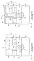
- a semiconductive material wafer fragment 10comprises a substrate 12 which supports an electrical node 14 .
- Substrate 12can comprise, for example, lightly doped monocrystalline silicon.
- Electrical node 14can comprise, for example, a conductively-doped diffusion region provided within a monocrystalline silicon substrate 12 .
- semiconductor substrateand “semiconductor substrate” are defined to mean any construction comprising semiconductive material, including, but not limited to, bulk semiconductive materials such as a semiconductive wafer (either alone or in assemblies comprising other materials thereon), and semiconductive material layers (either alone or in assemblies comprising other materials).
- substraterefers to any supporting structure, including, but not limited to, the semiconductive substrates described above.
- Insulative layer 16is formed over substrate 12 .
- Insulative layer 16can comprise, for example, silicon dioxide, silicon nitride, borophosphosilicate glass (BPSG), or phosphosilicate glass (PSG).
- Layer 16has an opening 18 extending therethrough to electrical node 14 .
- a conductive plug 20is provided within opening 18 .
- Conductive plug 20can comprise, for example, a metal, or conductively doped polysilicon.
- a container-shaped storage node 22is provided over insulative layer 16 , and over conductive plug 18 .
- Storage node 22is in electrical connection with electrical node 14 through conductive plug 18 .
- Container-shaped storage node 22can also be referred to as a crown-shaped storage node.
- Storage node 22comprises upwardly extending members 21 , and a horizontally extending member 23 .
- a dielectric material 24is provided over storage node 22
- a second capacitor electrode layer 26is provided over dielectric material 24 .
- Dielectric material 24can comprise, for example, a combination of silicon dioxide and silicon nitride.
- dielectric material 24can comprise tantalum pentoxide.
- Second capacitor electrode 26can comprise, for example, a metal, conductively doped polysilicon, or a metal-comprising compound, such as, for example, titanium nitride.
- Storage node 22 , dielectric material 24 , and second capacitor electrode 26together define a crown capacitor.
- a problem with the processing described above with reference to FIGS. 1 and 2is that the upwardly extending members 21 of storage node 22 can be easily broken during subsequent processing. It would therefore be desirable to develop alternative methods of forming crown capacitors.
- the inventionencompasses a method of forming a capacitor.
- a massis formed over an electrical node.
- An openingis formed within the mass.
- the openinghas a lower portion proximate the node and an upper portion above the lower portion. The lower portion is wider than the upper portion.
- a first conductive layeris formed within the opening and along a periphery of the opening. After the first conductive layer is formed, a portion of the mass is removed from beside the upper portion of the opening while another portion of the mass is left beside the lower portion of the opening.
- a dielectric materialis formed over the first conductive layer, and a second conductive layer is formed over the dielectric material. The second conductive layer is separated from the first conductive layer by the dielectric material.
- the inventionencompasses a capacitor construction.
- Such constructionincludes an insulative mass over an electrical node, and an opening extending through the mass to the electrical node.
- the constructionfurther includes a storage node layer within the opening.
- the storage node layerextends around a periphery of the opening and protrudes above the insulative mass.
- the storage node layerdefines a container shape having a void extending therein.
- the voidhas a lower portion within the opening and an upper portion above the opening. The upper portion of the void is narrower than the lower portion.
- the constructionincludes a dielectric material within the void and partially filling the void, and a second capacitor electrode within the void and separated from the first conductive layer by the dielectric material.
- FIG. 1is a diagrammatic, cross-sectional view of a semiconductive material wafer fragment shown at a preliminary step of a prior art capacitor-forming process.
- FIG. 2is a view of the FIG. 1 wafer fragment shown at a prior art processing step subsequent to that of FIG. 1.
- FIG. 3is a diagrammatic, cross-sectional view of a semiconductive material wafer fragment shown at a preliminary step of a capacitor-forming method encompassed by the present invention.
- FIG. 4is a view of the FIG. 3 wafer fragment shown at a processing step subsequent to that of FIG. 3.
- FIG. 5is a view of the FIG. 3 wafer fragment shown at a processing step subsequent to that of FIG. 4.
- FIG. 6is a view of the FIG. 3 wafer fragment shown at a processing step subsequent to that of FIG. 5.
- FIG. 7is a view of the FIG. 3 wafer fragment shown at a processing step subsequent to that of FIG. 6.
- FIG. 8is a view of the FIG. 3 wafer fragment shown at a processing step subsequent to that of FIG. 7.
- FIG. 9is a top view of the FIG. 8 wafer fragment.
- FIG. 10is a view of the FIG. 3 wafer fragment shown at a processing step subsequent to that of FIG. 8.
- FIG. 11is a view of the FIG. 3 wafer fragment shown at a second embodiment processing step subsequent to that of FIG. 5.
- FIG. 12is a view of the FIG. 3 wafer fragment shown at a processing step in accordance with the second embodiment and subsequent to that of FIG. 11.
- FIG. 13is a top view of the FIG. 12 wafer fragment.
- FIG. 14is a view of the FIG. 3 wafer fragment shown at a processing step in accordance with the second embodiment and subsequent to that of FIG. 12.
- FIG. 3A first embodiment method of forming a capacitor construction in accordance with the present invention is described with reference to FIGS. 3 - 10 .
- Wafer fragment 50comprises a substrate 52 supporting an electrical node 54 .
- Substrate 52 and node 54can comprise, for example, the constructions described above for substrate 12 and node 14 , respectively, of the prior art construction of FIG. 1.
- Substrate 52 and node 54can also, of course, comprise alternate constructions.
- Insulative material 56is formed over substrate 52 .
- Insulative material 56can comprise, for example, materials similar to those described above with reference to insulative layer 16 of the prior art construction of FIG. 1.
- An opening 58extends through insulative material 56 , and a conductive material 60 is formed within the opening.
- Conductive material 60can comprise, for example, constructions similar to those discussed above with reference to conductive plug 20 of the prior art construction of FIG. 1. Plug 60 can also comprise alternate constructions. It is noted that although the term “electrical node” was utilized above in describing node 54 , plug 60 can also be referred to as an “electrical node”.
- a mass 62is formed over insulative layer 56 and electrical node 60 .
- mass 62comprises the three distinct layers 64 , 66 and 68 .
- Layers 64 , 66 and 68preferably comprise materials selectively etchable relative to one another.
- layer 64consists essentially of PSG
- layer 66consists essentially of silicon nitride
- layer 68consists essentially of BPSG.
- layer 64consists essentially of doped silicon dioxide
- layer 66consists essentially of silicon nitride
- layer 68consists essentially of undoped silicon dioxide.
- Layers 64 and 66are preferably electrically insulative.
- Layers 64 , 66 and 68can be formed to thicknesses of, for example, about 100 nanometers, 10 nanometers and 400 nanometers, respectively.
- an opening 70is etched through layers 64 , 66 and 68 to expose node 60 .
- Such openingcan be formed by, for example, photolithographic processing to form a patterned photoresist mask (not shown) over layer 68 , and subsequently utilizing an etchant comprising a halogenated-hydro-carbon and inert gases to etch through layers 64 , 66 , and 68 in the location of opening 70 .
- the material of layer 64is etched faster than the materials of layers 66 and 68 .
- Such faster etchingcan be accomplished for an etch selective for the material of layer 64 relative to the materials of layers 66 and 68 .
- the selective etchingcan be accomplished utilizing hydrofluoric acid.
- the selective etchingcan be accomplished utilizing hydrofluoric acid.
- a hydrofluoric acid etchwould typically be done prior to formation of a storage node in contact with electrical node 60 (the storage node is described below with reference to FIGS. 6 - 10 ), to clean exposed portions of fragment 50 prior to formation of the storage node. Accordingly, the etching with hydrofluoric acid does not add an additional process step beyond the steps generally utilized for capacitor fabrication.
- opening 70comprises two distinct portions, labeled as portions 72 and 74 in FIG. 5.
- Portion 72is a lower portion, and portion 74 is an upper portion.
- Portions 72 and 74join at a lower edge of layer 66 .
- Lower portion 72has a width “Y” and upper portion 74 has a width “Z”, with “Z” being less than “Y”.
- First conductive layer 80is formed over mass 62 and within opening 70 .
- First conductive layer 80can comprise, for example, conductively doped polysilicon and/or a metal.
- First conductive layer 80preferably comprises conductively doped roughened polysilicon, such as, for example, conductively doped hemispherical grain polysilicon.
- First conductive layer 80only partially fills opening 70 and defines a void 86 therein.
- a masking material 82is formed over conductive layer 80 .
- Masking material 82is preferably applied while wafer 50 is spinning, and applied at a viscosity such that material 82 flows into opening 70 . Further, material 82 is preferably applied to a thickness such that opening 70 is predominately filled, but only a very thin amount of material 82 is over mass 62 .
- Material 82can comprise, for example, photoresist.
- wafer fragment 50is subjected to etching conditions which remove the thin layer of masking material 82 from over mass 62 , and subsequently remove first conductive layer 80 from over mass 62 .
- etching conditionswhich remove the thin layer of masking material 82 from over mass 62 , and subsequently remove first conductive layer 80 from over mass 62 .
- the portion of masking material 82 within opening 70protects first conductive layer 80 within opening 70 .
- the etchingforms first conductive layer 80 into a container-shape retained within opening 70 .
- the container-shapecan also be referred to as a crown-shape.
- FIGS. 6 and 7are but one exemplary method of removing conductive material 80 from over mass 62 while leaving some of conductive material 80 within opening 70 , and other methods will be recognized by persons of ordinary skill in the art.
- alternative methods of removing conductive material 80 from over mass 62include chemical-mechanical polishing and resist etch-back.
- wafer fragment 50is subjected to conditions which remove masking material 82 from within opening 70 .
- a mask material 82comprises photoresist
- such conditionscan comprise exposure to oxygen and heat sufficient to ash photoresist 82 .
- wafer fragment 50is subjected to conditions which remove layer 68 from over layer 66 .
- layer 66constitutes an etch-stop.
- the selective etching of layer 68 relative to layer 66can be accomplished utilizing hydrofluoric acid.
- the removal of layer 68reduces a height of mass 62 .
- the removal of layer 68increases the surface of the conductive material.
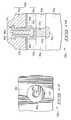
- FIG. 9shows a top view of the fragment 50 of FIG. 8, and shows that conductive material 80 is preferably in a container-shape comprising a circular opening 86 extending therein.
- dielectric material 90 , and a second conductive layer 92are formed over first conductive layer 80 and within void 86 .
- Dielectric material 90 and second conductive material 92can comprise, for example, materials similar to those discussed above regarding dielectric material 24 and conductive material 26 , respectively, of the prior art (FIG. 2).
- First conductive material 80 , dielectric layer 90 , and second conductive layer 92together define a capacitor, with first conductive material 80 corresponding to a storage node of the capacitor and second conductive material 92 corresponding to a second capacitor electrode.
- Second capacitor electrode 92is separated from storage node 80 by dielectric layer 90 .
- a portion of storage node 80is within mass 62 , and a portion extends above mass 62 . Accordingly, storage node 80 corresponds to a partially buried storage node.
- Storage node 80like prior art storage node 22 , comprises upwardly projecting portions (labeled as 100 for storage node 80 ), and a horizontal portion (labeled as 102 for storage node 80 ).
- the partially buried nature of capacitor 80provides structural support for vertically extending portions 100 beyond that provided for vertically extending portions 21 (FIG. 2) of a prior art capacitor construction achieving a same capacitance as the capacitor construction of FIG. 10. Such structural support can increase a mechanical stability of vertically projecting portions 100 relative to vertically projecting portions 21 .
- the partially-buried nature of a storage node of the present inventionreduces a non-planarity across an upper surface of wafer fragment 50 in the processing steps of FIGS. 8 - 10 relative to the non-planarity associated with an upper surface of wafer fragment 50 in prior art processing steps associated with FIGS. 1 and 2.
- Such reduction in non-planaritycan alleviate problems associated with photolithographic processing. Specifically, photolithographic processing becomes increasingly more complicated with increasing non-planarity across an upper surface that is to be patterned.
- FIGS. 11 - 14A second embodiment of the present invention is described with reference to FIGS. 11 - 14 .
- similar numberingwill be used as was utilized above in describing the first embodiments of FIGS. 3 - 10 , with the suffix “a” indicating structures associated with FIGS. 11 - 14 .
- Wafer fragment 50 ais illustrated at a processing step subsequent to the step illustrated in FIG. 5.
- Wafer fragment 50 acomprises a first conductive material 80 a formed over a mass 62 a and within an opening 70 a .
- Conductive material 80 aonly partially fills opening 70 a , and accordingly defines a void 86 a therein.
- Mass 62 acomprises layers 64 a , 66 a and 68 a.
- a masking material 82 ais formed within void 86 a and over mass 62 a , and patterned to cover only a portion of conductive material 80 a over mass 62 a .
- Masking material 82 acan comprise, for example, photoresist, and can be patterned by, for example, photolithographic processing.
- wafer fragment 50 ais subjected to etching conditions which remove exposed portions of conductive material 80 a from over mass 62 a .
- masking material 82 a(FIG. 11) is removed from within void 86 a .
- a portion of conductive material 80 aremains over mass 62 a .
- Such portiondefines a flange 150 .
- a top view of the construction of FIG. 12is shown in FIG. 13. As can be seen in such top view, flange 150 extends around an upper periphery of a storage node defined by layer 80 a.
- layer 68 a(FIG. 12) is removed. Subsequently, a dielectric material 90 a and a second conductive layer 92 a are formed over storage node 80 a and within void 86 a to form a capacitor construction analogous to the construction described above with reference to FIG. 10.
Landscapes
- Semiconductor Integrated Circuits (AREA)
- Semiconductor Memories (AREA)
Abstract
Description
- The invention pertains to capacitor constructions and methods of forming capacitors. In a particular aspect, the invention pertains to crown capacitor constructions.[0001]
- A method of forming a prior art crown capacitor construction is described with reference to FIGS. 1 and 2. Referring to FIG. 1, a semiconductive[0002]
material wafer fragment 10 comprises asubstrate 12 which supports anelectrical node 14.Substrate 12 can comprise, for example, lightly doped monocrystalline silicon.Electrical node 14 can comprise, for example, a conductively-doped diffusion region provided within amonocrystalline silicon substrate 12. - To aid in interpretation of the claims that follow, the terms “semiconductive substrate” and “semiconductor substrate” are defined to mean any construction comprising semiconductive material, including, but not limited to, bulk semiconductive materials such as a semiconductive wafer (either alone or in assemblies comprising other materials thereon), and semiconductive material layers (either alone or in assemblies comprising other materials). The term “substrate” refers to any supporting structure, including, but not limited to, the semiconductive substrates described above.[0003]
- An[0004]
insulative layer 16 is formed oversubstrate 12.Insulative layer 16 can comprise, for example, silicon dioxide, silicon nitride, borophosphosilicate glass (BPSG), or phosphosilicate glass (PSG).Layer 16 has anopening 18 extending therethrough toelectrical node 14. Aconductive plug 20 is provided within opening18.Conductive plug 20 can comprise, for example, a metal, or conductively doped polysilicon. - A container-[0005]
shaped storage node 22 is provided overinsulative layer 16, and overconductive plug 18.Storage node 22 is in electrical connection withelectrical node 14 throughconductive plug 18. Container-shaped storage node 22 can also be referred to as a crown-shaped storage node.Storage node 22 comprises upwardly extendingmembers 21, and a horizontally extendingmember 23. - Referring to FIG. 2, a[0006]
dielectric material 24 is provided overstorage node 22, and a secondcapacitor electrode layer 26 is provided overdielectric material 24.Dielectric material 24 can comprise, for example, a combination of silicon dioxide and silicon nitride. Alternatively,dielectric material 24 can comprise tantalum pentoxide.Second capacitor electrode 26 can comprise, for example, a metal, conductively doped polysilicon, or a metal-comprising compound, such as, for example, titanium nitride. - [0007]
Storage node 22,dielectric material 24, andsecond capacitor electrode 26, together define a crown capacitor. - A problem with the processing described above with reference to FIGS. 1 and 2 is that the upwardly extending[0008]
members 21 ofstorage node 22 can be easily broken during subsequent processing. It would therefore be desirable to develop alternative methods of forming crown capacitors. - In one aspect, the invention encompasses a method of forming a capacitor. A mass is formed over an electrical node. An opening is formed within the mass. The opening has a lower portion proximate the node and an upper portion above the lower portion. The lower portion is wider than the upper portion. A first conductive layer is formed within the opening and along a periphery of the opening. After the first conductive layer is formed, a portion of the mass is removed from beside the upper portion of the opening while another portion of the mass is left beside the lower portion of the opening. A dielectric material is formed over the first conductive layer, and a second conductive layer is formed over the dielectric material. The second conductive layer is separated from the first conductive layer by the dielectric material.[0009]
- In another aspect, the invention encompasses a capacitor construction. Such construction includes an insulative mass over an electrical node, and an opening extending through the mass to the electrical node. The construction further includes a storage node layer within the opening. The storage node layer extends around a periphery of the opening and protrudes above the insulative mass. The storage node layer defines a container shape having a void extending therein. The void has a lower portion within the opening and an upper portion above the opening. The upper portion of the void is narrower than the lower portion. Additionally, the construction includes a dielectric material within the void and partially filling the void, and a second capacitor electrode within the void and separated from the first conductive layer by the dielectric material.[0010]
- Preferred embodiments of the invention are described below with reference to the following accompanying drawings.[0011]
- FIG. 1 is a diagrammatic, cross-sectional view of a semiconductive material wafer fragment shown at a preliminary step of a prior art capacitor-forming process.[0012]
- FIG. 2 is a view of the FIG. 1 wafer fragment shown at a prior art processing step subsequent to that of FIG. 1.[0013]
- FIG. 3 is a diagrammatic, cross-sectional view of a semiconductive material wafer fragment shown at a preliminary step of a capacitor-forming method encompassed by the present invention.[0014]
- FIG. 4 is a view of the FIG. 3 wafer fragment shown at a processing step subsequent to that of FIG. 3.[0015]
- FIG. 5 is a view of the FIG. 3 wafer fragment shown at a processing step subsequent to that of FIG. 4.[0016]
- FIG. 6 is a view of the FIG. 3 wafer fragment shown at a processing step subsequent to that of FIG. 5.[0017]
- FIG. 7 is a view of the FIG. 3 wafer fragment shown at a processing step subsequent to that of FIG. 6.[0018]
- FIG. 8 is a view of the FIG. 3 wafer fragment shown at a processing step subsequent to that of FIG. 7.[0019]
- FIG. 9 is a top view of the FIG. 8 wafer fragment.[0020]
- FIG. 10 is a view of the FIG. 3 wafer fragment shown at a processing step subsequent to that of FIG. 8.[0021]
- FIG. 11 is a view of the FIG. 3 wafer fragment shown at a second embodiment processing step subsequent to that of FIG. 5.[0022]
- FIG. 12 is a view of the FIG. 3 wafer fragment shown at a processing step in accordance with the second embodiment and subsequent to that of FIG. 11.[0023]
- FIG. 13 is a top view of the FIG. 12 wafer fragment.[0024]
- FIG. 14 is a view of the FIG. 3 wafer fragment shown at a processing step in accordance with the second embodiment and subsequent to that of FIG. 12.[0025]
- This disclosure of the invention is submitted in furtherance of the constitutional purposes of the U.S. Patent Laws “to promote the progress of science and useful arts” (Article 1, Section 8).[0026]
- A first embodiment method of forming a capacitor construction in accordance with the present invention is described with reference to FIGS.[0027]3-10. Referring to FIG. 3, a semiconductive
material wafer fragment 50 is shown at a preliminary process step. Waferfragment 50 comprises asubstrate 52 supporting anelectrical node 54.Substrate 52 andnode 54 can comprise, for example, the constructions described above forsubstrate 12 andnode 14, respectively, of the prior art construction of FIG. 1.Substrate 52 andnode 54 can also, of course, comprise alternate constructions. - An[0028]
insulative material 56 is formed oversubstrate 52.Insulative material 56 can comprise, for example, materials similar to those described above with reference toinsulative layer 16 of the prior art construction of FIG. 1. Anopening 58 extends throughinsulative material 56, and aconductive material 60 is formed within the opening.Conductive material 60 can comprise, for example, constructions similar to those discussed above with reference toconductive plug 20 of the prior art construction of FIG. 1.Plug 60 can also comprise alternate constructions. It is noted that although the term “electrical node” was utilized above in describingnode 54, plug60 can also be referred to as an “electrical node”. - A[0029]
mass 62 is formed overinsulative layer 56 andelectrical node 60. In the shown embodiment,mass 62 comprises the threedistinct layers Layers embodiment layer 64 consists essentially of PSG,layer 66 consists essentially of silicon nitride, andlayer 68 consists essentially of BPSG. In another embodiment,layer 64 consists essentially of doped silicon dioxide,layer 66 consists essentially of silicon nitride, andlayer 68 consists essentially of undoped silicon dioxide.Layers Layers - Referring to FIG. 4, an[0030]
opening 70 is etched throughlayers node 60. Such opening can be formed by, for example, photolithographic processing to form a patterned photoresist mask (not shown) overlayer 68, and subsequently utilizing an etchant comprising a halogenated-hydro-carbon and inert gases to etch throughlayers - Referring to FIG. 5, the material of[0031]
layer 64 is etched faster than the materials oflayers layer 64 relative to the materials oflayers layer 64 comprises PSG, and the materials oflayer layer 64 comprises doped silicon dioxide, and layers66 and68 comprise silicon nitride and undoped silicon dioxide, respectively, the selective etching can be accomplished utilizing hydrofluoric acid. It is noted that a hydrofluoric acid etch would typically be done prior to formation of a storage node in contact with electrical node60 (the storage node is described below with reference to FIGS.6-10), to clean exposed portions offragment 50 prior to formation of the storage node. Accordingly, the etching with hydrofluoric acid does not add an additional process step beyond the steps generally utilized for capacitor fabrication. - After the etching of[0032]
layer 64, opening70 comprises two distinct portions, labeled asportions Portion 72 is a lower portion, andportion 74 is an upper portion.Portions layer 66.Lower portion 72 has a width “Y” andupper portion 74 has a width “Z”, with “Z” being less than “Y”. - Referring to FIG. 6, a first[0033]
conductive layer 80 is formed overmass 62 and withinopening 70. Firstconductive layer 80 can comprise, for example, conductively doped polysilicon and/or a metal. Firstconductive layer 80 preferably comprises conductively doped roughened polysilicon, such as, for example, conductively doped hemispherical grain polysilicon. Firstconductive layer 80 only partially fills opening70 and defines a void86 therein. - A masking[0034]
material 82 is formed overconductive layer 80. Maskingmaterial 82 is preferably applied whilewafer 50 is spinning, and applied at a viscosity such thatmaterial 82 flows intoopening 70. Further,material 82 is preferably applied to a thickness such thatopening 70 is predominately filled, but only a very thin amount ofmaterial 82 is overmass 62.Material 82 can comprise, for example, photoresist. - Referring to FIG. 7,[0035]
wafer fragment 50 is subjected to etching conditions which remove the thin layer of maskingmaterial 82 from overmass 62, and subsequently remove firstconductive layer 80 from overmass 62. During such etching, the portion of maskingmaterial 82 withinopening 70 protects firstconductive layer 80 withinopening 70. Accordingly, the etching forms firstconductive layer 80 into a container-shape retained withinopening 70. The container-shape can also be referred to as a crown-shape. - The methodologies of FIGS. 6 and 7 are but one exemplary method of removing[0036]
conductive material 80 from overmass 62 while leaving some ofconductive material 80 withinopening 70, and other methods will be recognized by persons of ordinary skill in the art. For instance, alternative methods of removingconductive material 80 from overmass 62 include chemical-mechanical polishing and resist etch-back. - Referring to FIG. 8,[0037]
wafer fragment 50 is subjected to conditions which remove maskingmaterial 82 from withinopening 70. In exemplary embodiments where amask material 82 comprises photoresist, such conditions can comprise exposure to oxygen and heat sufficient toash photoresist 82. Also,wafer fragment 50 is subjected to conditions which removelayer 68 from overlayer 66. In preferred embodiments whereinlayer 68 is selectively etchable relative to layer66,layer 66 constitutes an etch-stop. In an exemplary embodiment whereinlayer 68 comprises undoped silicon oxide andlayer 66 comprises silicon nitride, the selective etching oflayer 68 relative to layer66 can be accomplished utilizing hydrofluoric acid. The removal oflayer 68 reduces a height ofmass 62. The removal oflayer 68 increases the surface of the conductive material. - FIG. 9 shows a top view of the[0038]
fragment 50 of FIG. 8, and shows thatconductive material 80 is preferably in a container-shape comprising acircular opening 86 extending therein. - Referring to FIG. 10,[0039]
dielectric material 90, and a secondconductive layer 92 are formed over firstconductive layer 80 and withinvoid 86.Dielectric material 90 and secondconductive material 92 can comprise, for example, materials similar to those discussed above regardingdielectric material 24 andconductive material 26, respectively, of the prior art (FIG. 2). Firstconductive material 80,dielectric layer 90, and secondconductive layer 92 together define a capacitor, with firstconductive material 80 corresponding to a storage node of the capacitor and secondconductive material 92 corresponding to a second capacitor electrode.Second capacitor electrode 92 is separated fromstorage node 80 bydielectric layer 90. - In the shown embodiment, a portion of[0040]
storage node 80 is withinmass 62, and a portion extends abovemass 62. Accordingly,storage node 80 corresponds to a partially buried storage node.Storage node 80, like priorart storage node 22, comprises upwardly projecting portions (labeled as100 for storage node80), and a horizontal portion (labeled as102 for storage node80). However, the partially buried nature ofcapacitor 80 provides structural support for vertically extendingportions 100 beyond that provided for vertically extending portions21 (FIG. 2) of a prior art capacitor construction achieving a same capacitance as the capacitor construction of FIG. 10. Such structural support can increase a mechanical stability of vertically projectingportions 100 relative to vertically projectingportions 21. Also, the partially-buried nature of a storage node of the present invention reduces a non-planarity across an upper surface ofwafer fragment 50 in the processing steps of FIGS.8-10 relative to the non-planarity associated with an upper surface ofwafer fragment 50 in prior art processing steps associated with FIGS. 1 and 2. Such reduction in non-planarity can alleviate problems associated with photolithographic processing. Specifically, photolithographic processing becomes increasingly more complicated with increasing non-planarity across an upper surface that is to be patterned. - A second embodiment of the present invention is described with reference to FIGS.[0041]11-14. In referring to FIGS.11-14, similar numbering will be used as was utilized above in describing the first embodiments of FIGS.3-10, with the suffix “a” indicating structures associated with FIGS.11-14.
- Referring to FIG. 11, a semiconductive material wafer fragment[0042]50ais illustrated at a processing step subsequent to the step illustrated in FIG. 5. Wafer fragment50acomprises a first conductive material80aformed over a mass62aand within an opening70a. Conductive material80aonly partially fills opening70a, and accordingly defines a void86atherein.
Mass 62acompriseslayers - A masking[0043]
material 82ais formed withinvoid 86aand overmass 62a, and patterned to cover only a portion of conductive material80aovermass 62a. Maskingmaterial 82acan comprise, for example, photoresist, and can be patterned by, for example, photolithographic processing. - Referring to FIG. 12, wafer fragment[0044]50ais subjected to etching conditions which remove exposed portions of conductive material80afrom over
mass 62a. Subsequently, maskingmaterial 82a(FIG. 11) is removed from withinvoid 86a. In the shown embodiment, a portion of conductive material80aremains over mass62a. Such portion defines aflange 150. A top view of the construction of FIG. 12 is shown in FIG. 13. As can be seen in such top view,flange 150 extends around an upper periphery of a storage node defined by layer80a. - Referring to FIG. 14,[0045]
layer 68a(FIG. 12) is removed. Subsequently, a dielectric material90aand a secondconductive layer 92aare formed over storage node80aand withinvoid 86ato form a capacitor construction analogous to the construction described above with reference to FIG. 10. - In compliance with the statute, the invention has been described in language more or less specific as to structural and methodical features. It is to be understood, however, that the invention is not limited to the specific features shown and described, since the means herein disclosed comprise preferred forms of putting the invention into effect. The invention is, therefore, claimed in any of its forms or modifications within the proper scope of the appended claims appropriately interpreted in accordance with the doctrine of equivalents.[0046]
Claims (29)
Priority Applications (1)
| Application Number | Priority Date | Filing Date | Title |
|---|---|---|---|
| US09/729,130US6627938B2 (en) | 1999-08-30 | 2000-12-01 | Capacitor constructions |
Applications Claiming Priority (2)
| Application Number | Priority Date | Filing Date | Title |
|---|---|---|---|
| US09/386,537US6429087B2 (en) | 1999-08-30 | 1999-08-30 | Methods of forming capacitors |
| US09/729,130US6627938B2 (en) | 1999-08-30 | 2000-12-01 | Capacitor constructions |
Related Parent Applications (1)
| Application Number | Title | Priority Date | Filing Date |
|---|---|---|---|
| US09/386,537DivisionUS6429087B2 (en) | 1999-08-30 | 1999-08-30 | Methods of forming capacitors |
Publications (2)
| Publication Number | Publication Date |
|---|---|
| US20010002053A1true US20010002053A1 (en) | 2001-05-31 |
| US6627938B2 US6627938B2 (en) | 2003-09-30 |
Family
ID=23526008
Family Applications (2)
| Application Number | Title | Priority Date | Filing Date |
|---|---|---|---|
| US09/386,537Expired - LifetimeUS6429087B2 (en) | 1999-08-30 | 1999-08-30 | Methods of forming capacitors |
| US09/729,130Expired - LifetimeUS6627938B2 (en) | 1999-08-30 | 2000-12-01 | Capacitor constructions |
Family Applications Before (1)
| Application Number | Title | Priority Date | Filing Date |
|---|---|---|---|
| US09/386,537Expired - LifetimeUS6429087B2 (en) | 1999-08-30 | 1999-08-30 | Methods of forming capacitors |
Country Status (1)
| Country | Link |
|---|---|
| US (2) | US6429087B2 (en) |
Cited By (5)
| Publication number | Priority date | Publication date | Assignee | Title |
|---|---|---|---|---|
| FR2837624A1 (en)* | 2002-03-20 | 2003-09-26 | Memscap | ELECTRONIC MICRO-COMPONENT WITH INTEGRATED CAPACITIVE STRUCTURE, AND MANUFACTURING METHOD |
| US6756265B2 (en) | 2001-08-20 | 2004-06-29 | Micron Technology, Inc. | Methods of forming a capacitor structure |
| US20040150021A1 (en)* | 2003-01-17 | 2004-08-05 | Fujitsu Limited | Semiconductor device suitable for forming conductive film such as platinum with good coverage, and its manufacture |
| US20060131632A1 (en)* | 2004-12-22 | 2006-06-22 | Samsung Electronics Co., Ltd. | Dram device having capacitor and method thereof |
| US20210050353A1 (en)* | 2018-05-28 | 2021-02-18 | United Microelectronics Corp. | Semiconductor memory device |
Families Citing this family (13)
| Publication number | Priority date | Publication date | Assignee | Title |
|---|---|---|---|---|
| US6319789B1 (en)* | 1999-01-25 | 2001-11-20 | Micron Techonology, Inc. | Method for improved processing and etchback of a container capacitor |
| KR100388683B1 (en)* | 2001-03-06 | 2003-06-25 | 삼성전자주식회사 | Method for manufacturing capacitor in semiconductor device |
| TWI271872B (en)* | 2002-12-30 | 2007-01-21 | Hynix Semiconductor Inc | Capacitor and method for fabricating the same |
| KR100721579B1 (en)* | 2002-12-30 | 2007-05-23 | 주식회사 하이닉스반도체 | Manufacturing method of capacitor |
| TWI221657B (en)* | 2003-05-30 | 2004-10-01 | Nanya Technology Corp | Method of forming crown capacitor |
| US7224014B2 (en)* | 2003-12-05 | 2007-05-29 | Matsushita Electric Industrial Co., Ltd. | Semiconductor device and method for fabricating the same |
| US7442600B2 (en) | 2004-08-24 | 2008-10-28 | Micron Technology, Inc. | Methods of forming threshold voltage implant regions |
| US7449739B2 (en)* | 2006-01-25 | 2008-11-11 | Infineon Technologies Ag | Storage capacitor for semiconductor memory cells and method of manufacturing a storage capacitor |
| TW200824096A (en)* | 2006-11-28 | 2008-06-01 | Promos Technologies Inc | Method of fabricating capacitor and electrode thereof |
| KR100914290B1 (en) | 2007-10-29 | 2009-08-27 | 주식회사 하이닉스반도체 | Capacitor Formation Method of Semiconductor Device |
| KR101003490B1 (en) | 2007-10-29 | 2010-12-30 | 주식회사 하이닉스반도체 | Capacitor Formation Method of Semiconductor Device |
| KR20110135770A (en)* | 2010-06-11 | 2011-12-19 | 삼성전자주식회사 | Manufacturing Method of Semiconductor Device |
| CN102456613B (en)* | 2010-10-29 | 2014-08-20 | 中国科学院微电子研究所 | Semiconductor structure and manufacturing method thereof |
Citations (4)
| Publication number | Priority date | Publication date | Assignee | Title |
|---|---|---|---|---|
| US5436188A (en)* | 1994-04-26 | 1995-07-25 | Industrial Technology Research Institute | Dram cell process having elk horn shaped capacitor |
| US5545585A (en)* | 1996-01-29 | 1996-08-13 | Taiwan Semiconductor Manufacturing Company | Method of making a dram circuit with fin-shaped stacked capacitors |
| US6043119A (en)* | 1997-08-04 | 2000-03-28 | Micron Technology, Inc. | Method of making a capacitor |
| US6335552B1 (en)* | 1995-01-31 | 2002-01-01 | Fujitsu Limited | Semiconductor device and method for fabricating the same |
Family Cites Families (8)
| Publication number | Priority date | Publication date | Assignee | Title |
|---|---|---|---|---|
| US5391511A (en) | 1992-02-19 | 1995-02-21 | Micron Technology, Inc. | Semiconductor processing method of producing an isolated polysilicon lined cavity and a method of forming a capacitor |
| US5604147A (en)* | 1995-05-12 | 1997-02-18 | Micron Technology, Inc. | Method of forming a cylindrical container stacked capacitor |
| US5597756A (en)* | 1995-06-21 | 1997-01-28 | Micron Technology, Inc. | Process for fabricating a cup-shaped DRAM capacitor using a multi-layer partly-sacrificial stack |
| US6214727B1 (en) | 1997-02-11 | 2001-04-10 | Micron Technology, Inc. | Conductive electrical contacts, capacitors, DRAMs, and integrated circuitry, and methods of forming conductive electrical contacts, capacitors, DRAMs, and integrated circuitry |
| US6046093A (en)* | 1997-06-13 | 2000-04-04 | Micron Technololgy, Inc. | Method of forming capacitors and related integrated circuitry |
| US5821141A (en)* | 1998-01-12 | 1998-10-13 | Taiwan Semiconductor Manufacturing Company, Ltd | Method for forming a cylindrical capacitor in DRAM having pin plug profile |
| US6080620A (en)* | 1998-06-03 | 2000-06-27 | Vanguard International Semiconductor Corporation | Method for fabricating interconnection and capacitors of a DRAM using a simple geometry active area, self-aligned etching, and polysilicon plugs |
| US6107139A (en)* | 1998-07-17 | 2000-08-22 | Worldwide Semiconductor Manufacturing Corporation | Method for making a mushroom shaped DRAM capacitor |
- 1999
- 1999-08-30USUS09/386,537patent/US6429087B2/ennot_activeExpired - Lifetime
- 2000
- 2000-12-01USUS09/729,130patent/US6627938B2/ennot_activeExpired - Lifetime
Patent Citations (4)
| Publication number | Priority date | Publication date | Assignee | Title |
|---|---|---|---|---|
| US5436188A (en)* | 1994-04-26 | 1995-07-25 | Industrial Technology Research Institute | Dram cell process having elk horn shaped capacitor |
| US6335552B1 (en)* | 1995-01-31 | 2002-01-01 | Fujitsu Limited | Semiconductor device and method for fabricating the same |
| US5545585A (en)* | 1996-01-29 | 1996-08-13 | Taiwan Semiconductor Manufacturing Company | Method of making a dram circuit with fin-shaped stacked capacitors |
| US6043119A (en)* | 1997-08-04 | 2000-03-28 | Micron Technology, Inc. | Method of making a capacitor |
Cited By (12)
| Publication number | Priority date | Publication date | Assignee | Title |
|---|---|---|---|---|
| US6756265B2 (en) | 2001-08-20 | 2004-06-29 | Micron Technology, Inc. | Methods of forming a capacitor structure |
| US6949427B2 (en) | 2001-08-20 | 2005-09-27 | Micron Technology, Inc. | Methods of forming a capacitor structure |
| US7023039B2 (en)* | 2001-08-20 | 2006-04-04 | Micron Technology, Inc. | Capacitor structures with dual-sided electrode |
| FR2837624A1 (en)* | 2002-03-20 | 2003-09-26 | Memscap | ELECTRONIC MICRO-COMPONENT WITH INTEGRATED CAPACITIVE STRUCTURE, AND MANUFACTURING METHOD |
| US20040150021A1 (en)* | 2003-01-17 | 2004-08-05 | Fujitsu Limited | Semiconductor device suitable for forming conductive film such as platinum with good coverage, and its manufacture |
| US7102189B2 (en) | 2003-01-17 | 2006-09-05 | Fujitsu Limited | Semiconductor device suitable for forming conductive film such as platinum with good coverage, and its manufacture |
| US20060286744A1 (en)* | 2003-01-17 | 2006-12-21 | Fujitsu Limited | Semiconductor device suitable for forming conductive film such as platinum with good coverage, and its manufacture |
| US7470595B2 (en) | 2003-01-17 | 2008-12-30 | Fujitsu Limited | Oxidizing a metal layer for a dielectric having a platinum electrode |
| US20060131632A1 (en)* | 2004-12-22 | 2006-06-22 | Samsung Electronics Co., Ltd. | Dram device having capacitor and method thereof |
| US7525143B2 (en) | 2004-12-22 | 2009-04-28 | Samsung Electronics Co., Ltd | Dram device having capacitor |
| US20210050353A1 (en)* | 2018-05-28 | 2021-02-18 | United Microelectronics Corp. | Semiconductor memory device |
| US11943909B2 (en)* | 2018-05-28 | 2024-03-26 | United Microelectronics Corp. | Semiconductor memory device |
Also Published As
| Publication number | Publication date |
|---|---|
| US6429087B2 (en) | 2002-08-06 |
| US20020019106A1 (en) | 2002-02-14 |
| US6627938B2 (en) | 2003-09-30 |
Similar Documents
| Publication | Publication Date | Title |
|---|---|---|
| US6429087B2 (en) | Methods of forming capacitors | |
| US6492243B2 (en) | Methods of forming capacitors and resultant capacitor structures | |
| US5998257A (en) | Semiconductor processing methods of forming integrated circuitry memory devices, methods of forming capacitor containers, methods of making electrical connection to circuit nodes and related integrated circuitry | |
| US6693320B1 (en) | Capacitor structures with recessed hemispherical grain silicon | |
| KR100270211B1 (en) | Dram cell capacitor and method of fabricating the same | |
| US6307730B1 (en) | Capacitor formed by lower electrode having inner and outer uneven surfaces | |
| US6406967B1 (en) | Method for manufacturing cylindrical storage electrode of semiconductor device | |
| US6238968B1 (en) | Methods of forming integrated circuit capacitors having protected layers of HSG silicon therein | |
| JP3999403B2 (en) | Method for manufacturing DRAM cell capacitor | |
| US20110045650A1 (en) | Method of manufacturing semiconductor device | |
| US5966611A (en) | Semiconductor processing for forming capacitors by etching polysilicon and coating layer formed over the polysilicon | |
| CN100454549C (en) | Semiconductor capacitor structure and manufacturing method thereof | |
| US7022569B2 (en) | Lower electrode contact structure and method of forming the same | |
| JPH11330398A (en) | Method of forming buried plate and method of forming trench capacitor in silicon substrate | |
| KR20020043815A (en) | Manufacturing method of hemispherical grain capacitor | |
| US6534377B2 (en) | Capacitance elements and method of manufacturing the same | |
| US20030183865A1 (en) | Capacitor structure and method for fabricating the same | |
| JP3435849B2 (en) | Method for manufacturing semiconductor device | |
| US6274477B1 (en) | Method of fabricating conductive line structure | |
| KR100663338B1 (en) | Capacitor Manufacturing Method of Memory Cells | |
| JPH11330400A (en) | Method of manufacturing dynamic RAM cell capacitor | |
| KR100419748B1 (en) | Method of manufacturing semiconductor device | |
| KR100466982B1 (en) | Semiconductor device having capacitors and method of fabricating the same | |
| US20100081248A1 (en) | Method for manufacturing semiconductor device | |
| JP2002134711A (en) | Method for manufacturing semiconductor device |
Legal Events
| Date | Code | Title | Description |
|---|---|---|---|
| STCF | Information on status: patent grant | Free format text:PATENTED CASE | |
| FEPP | Fee payment procedure | Free format text:PAYOR NUMBER ASSIGNED (ORIGINAL EVENT CODE: ASPN); ENTITY STATUS OF PATENT OWNER: LARGE ENTITY | |
| FPAY | Fee payment | Year of fee payment:4 | |
| AS | Assignment | Owner name:MOSAID TECHNOLOGIES INCORPORATED, CANADA Free format text:ASSIGNMENT OF ASSIGNORS INTEREST;ASSIGNOR:MICRON TECHNOLOGY, INC.;REEL/FRAME:023220/0243 Effective date:20090609 | |
| FEPP | Fee payment procedure | Free format text:PAYOR NUMBER ASSIGNED (ORIGINAL EVENT CODE: ASPN); ENTITY STATUS OF PATENT OWNER: LARGE ENTITY Free format text:PAYER NUMBER DE-ASSIGNED (ORIGINAL EVENT CODE: RMPN); ENTITY STATUS OF PATENT OWNER: LARGE ENTITY | |
| AS | Assignment | Owner name:MOSAID TECHNOLOGIES INCORPORATED,CANADA Free format text:CORRECTIVE ASSIGNMENT TO CORRECT THE TO CORRECT THE ASSIGNEES' ADDRESS PREVIOUSLY RECORDED ON REEL 023220 FRAME 0243. ASSIGNOR(S) HEREBY CONFIRMS THE MOSAID TECHNOLOGIES INCORPORATED 6 SAUBLE DRIVE, SUITE 203, OTTAWA,ONTARIO, CANADA K2K 2X1;ASSIGNOR:MICRON TECHNOLOGY, INC.;REEL/FRAME:024225/0878 Effective date:20090609 | |
| FPAY | Fee payment | Year of fee payment:8 | |
| AS | Assignment | Owner name:ROYAL BANK OF CANADA, CANADA Free format text:U.S. INTELLECTUAL PROPERTY SECURITY AGREEMENT (FOR NON-U.S. GRANTORS) - SHORT FORM;ASSIGNORS:658276 N.B. LTD.;658868 N.B. INC.;MOSAID TECHNOLOGIES INCORPORATED;REEL/FRAME:027512/0196 Effective date:20111223 | |
| AS | Assignment | Owner name:CONVERSANT INTELLECTUAL PROPERTY MANAGEMENT INC., Free format text:CHANGE OF NAME;ASSIGNOR:MOSAID TECHNOLOGIES INCORPORATED;REEL/FRAME:032439/0638 Effective date:20140101 | |
| AS | Assignment | Owner name:CONVERSANT IP N.B. 868 INC., CANADA Free format text:RELEASE OF SECURITY INTEREST;ASSIGNOR:ROYAL BANK OF CANADA;REEL/FRAME:033484/0344 Effective date:20140611 Owner name:CONVERSANT IP N.B. 276 INC., CANADA Free format text:RELEASE OF SECURITY INTEREST;ASSIGNOR:ROYAL BANK OF CANADA;REEL/FRAME:033484/0344 Effective date:20140611 Owner name:CONVERSANT INTELLECTUAL PROPERTY MANAGEMENT INC., Free format text:RELEASE OF SECURITY INTEREST;ASSIGNOR:ROYAL BANK OF CANADA;REEL/FRAME:033484/0344 Effective date:20140611 | |
| AS | Assignment | Owner name:CONVERSANT INTELLECTUAL PROPERTY MANAGEMENT INC., CANADA Free format text:CHANGE OF ADDRESS;ASSIGNOR:CONVERSANT INTELLECTUAL PROPERTY MANAGEMENT INC.;REEL/FRAME:033678/0096 Effective date:20140820 Owner name:CONVERSANT INTELLECTUAL PROPERTY MANAGEMENT INC., Free format text:CHANGE OF ADDRESS;ASSIGNOR:CONVERSANT INTELLECTUAL PROPERTY MANAGEMENT INC.;REEL/FRAME:033678/0096 Effective date:20140820 | |
| AS | Assignment | Owner name:ROYAL BANK OF CANADA, AS LENDER, CANADA Free format text:U.S. PATENT SECURITY AGREEMENT (FOR NON-U.S. GRANTORS);ASSIGNOR:CONVERSANT INTELLECTUAL PROPERTY MANAGEMENT INC.;REEL/FRAME:033706/0367 Effective date:20140611 Owner name:CPPIB CREDIT INVESTMENTS INC., AS LENDER, CANADA Free format text:U.S. PATENT SECURITY AGREEMENT (FOR NON-U.S. GRANTORS);ASSIGNOR:CONVERSANT INTELLECTUAL PROPERTY MANAGEMENT INC.;REEL/FRAME:033706/0367 Effective date:20140611 | |
| FPAY | Fee payment | Year of fee payment:12 | |
| AS | Assignment | Owner name:CPPIB CREDIT INVESTMENTS, INC., CANADA Free format text:AMENDED AND RESTATED U.S. PATENT SECURITY AGREEMENT (FOR NON-U.S. GRANTORS);ASSIGNOR:CONVERSANT INTELLECTUAL PROPERTY MANAGEMENT INC.;REEL/FRAME:046900/0136 Effective date:20180731 | |
| AS | Assignment | Owner name:CONVERSANT INTELLECTUAL PROPERTY MANAGEMENT INC., CANADA Free format text:RELEASE OF U.S. PATENT AGREEMENT (FOR NON-U.S. GRANTORS);ASSIGNOR:ROYAL BANK OF CANADA, AS LENDER;REEL/FRAME:047645/0424 Effective date:20180731 Owner name:CONVERSANT INTELLECTUAL PROPERTY MANAGEMENT INC., Free format text:RELEASE OF U.S. PATENT AGREEMENT (FOR NON-U.S. GRANTORS);ASSIGNOR:ROYAL BANK OF CANADA, AS LENDER;REEL/FRAME:047645/0424 Effective date:20180731 | |
| AS | Assignment | Owner name:CONVERSANT INTELLECTUAL PROPERTY MANAGEMENT INC., CANADA Free format text:RELEASE BY SECURED PARTY;ASSIGNOR:CPPIB CREDIT INVESTMENTS INC.;REEL/FRAME:054372/0281 Effective date:20201028 |