US12351914B2 - Deposition of films using molybdenum precursors - Google Patents
Deposition of films using molybdenum precursorsDownload PDFInfo
- Publication number
- US12351914B2 US12351914B2US17/814,206US202217814206AUS12351914B2US 12351914 B2US12351914 B2US 12351914B2US 202217814206 AUS202217814206 AUS 202217814206AUS 12351914 B2US12351914 B2US 12351914B2
- Authority
- US
- United States
- Prior art keywords
- layer
- molybdenum
- metal
- deposition
- reducing agent
- Prior art date
- Legal status (The legal status is an assumption and is not a legal conclusion. Google has not performed a legal analysis and makes no representation as to the accuracy of the status listed.)
- Active
Links
Images


Classifications
- C—CHEMISTRY; METALLURGY
- C23—COATING METALLIC MATERIAL; COATING MATERIAL WITH METALLIC MATERIAL; CHEMICAL SURFACE TREATMENT; DIFFUSION TREATMENT OF METALLIC MATERIAL; COATING BY VACUUM EVAPORATION, BY SPUTTERING, BY ION IMPLANTATION OR BY CHEMICAL VAPOUR DEPOSITION, IN GENERAL; INHIBITING CORROSION OF METALLIC MATERIAL OR INCRUSTATION IN GENERAL
- C23C—COATING METALLIC MATERIAL; COATING MATERIAL WITH METALLIC MATERIAL; SURFACE TREATMENT OF METALLIC MATERIAL BY DIFFUSION INTO THE SURFACE, BY CHEMICAL CONVERSION OR SUBSTITUTION; COATING BY VACUUM EVAPORATION, BY SPUTTERING, BY ION IMPLANTATION OR BY CHEMICAL VAPOUR DEPOSITION, IN GENERAL
- C23C16/00—Chemical coating by decomposition of gaseous compounds, without leaving reaction products of surface material in the coating, i.e. chemical vapour deposition [CVD] processes
- C23C16/44—Chemical coating by decomposition of gaseous compounds, without leaving reaction products of surface material in the coating, i.e. chemical vapour deposition [CVD] processes characterised by the method of coating
- C23C16/455—Chemical coating by decomposition of gaseous compounds, without leaving reaction products of surface material in the coating, i.e. chemical vapour deposition [CVD] processes characterised by the method of coating characterised by the method used for introducing gases into reaction chamber or for modifying gas flows in reaction chamber
- C23C16/45523—Pulsed gas flow or change of composition over time
- C23C16/45525—Atomic layer deposition [ALD]
- C23C16/45553—Atomic layer deposition [ALD] characterized by the use of precursors specially adapted for ALD
- C—CHEMISTRY; METALLURGY
- C23—COATING METALLIC MATERIAL; COATING MATERIAL WITH METALLIC MATERIAL; CHEMICAL SURFACE TREATMENT; DIFFUSION TREATMENT OF METALLIC MATERIAL; COATING BY VACUUM EVAPORATION, BY SPUTTERING, BY ION IMPLANTATION OR BY CHEMICAL VAPOUR DEPOSITION, IN GENERAL; INHIBITING CORROSION OF METALLIC MATERIAL OR INCRUSTATION IN GENERAL
- C23C—COATING METALLIC MATERIAL; COATING MATERIAL WITH METALLIC MATERIAL; SURFACE TREATMENT OF METALLIC MATERIAL BY DIFFUSION INTO THE SURFACE, BY CHEMICAL CONVERSION OR SUBSTITUTION; COATING BY VACUUM EVAPORATION, BY SPUTTERING, BY ION IMPLANTATION OR BY CHEMICAL VAPOUR DEPOSITION, IN GENERAL
- C23C16/00—Chemical coating by decomposition of gaseous compounds, without leaving reaction products of surface material in the coating, i.e. chemical vapour deposition [CVD] processes
- C23C16/06—Chemical coating by decomposition of gaseous compounds, without leaving reaction products of surface material in the coating, i.e. chemical vapour deposition [CVD] processes characterised by the deposition of metallic material
- C23C16/08—Chemical coating by decomposition of gaseous compounds, without leaving reaction products of surface material in the coating, i.e. chemical vapour deposition [CVD] processes characterised by the deposition of metallic material from metal halides
- C23C16/14—Deposition of only one other metal element
- C—CHEMISTRY; METALLURGY
- C23—COATING METALLIC MATERIAL; COATING MATERIAL WITH METALLIC MATERIAL; CHEMICAL SURFACE TREATMENT; DIFFUSION TREATMENT OF METALLIC MATERIAL; COATING BY VACUUM EVAPORATION, BY SPUTTERING, BY ION IMPLANTATION OR BY CHEMICAL VAPOUR DEPOSITION, IN GENERAL; INHIBITING CORROSION OF METALLIC MATERIAL OR INCRUSTATION IN GENERAL
- C23C—COATING METALLIC MATERIAL; COATING MATERIAL WITH METALLIC MATERIAL; SURFACE TREATMENT OF METALLIC MATERIAL BY DIFFUSION INTO THE SURFACE, BY CHEMICAL CONVERSION OR SUBSTITUTION; COATING BY VACUUM EVAPORATION, BY SPUTTERING, BY ION IMPLANTATION OR BY CHEMICAL VAPOUR DEPOSITION, IN GENERAL
- C23C16/00—Chemical coating by decomposition of gaseous compounds, without leaving reaction products of surface material in the coating, i.e. chemical vapour deposition [CVD] processes
- C23C16/22—Chemical coating by decomposition of gaseous compounds, without leaving reaction products of surface material in the coating, i.e. chemical vapour deposition [CVD] processes characterised by the deposition of inorganic material, other than metallic material
- C23C16/30—Deposition of compounds, mixtures or solid solutions, e.g. borides, carbides, nitrides
- C23C16/308—Oxynitrides
- C—CHEMISTRY; METALLURGY
- C23—COATING METALLIC MATERIAL; COATING MATERIAL WITH METALLIC MATERIAL; CHEMICAL SURFACE TREATMENT; DIFFUSION TREATMENT OF METALLIC MATERIAL; COATING BY VACUUM EVAPORATION, BY SPUTTERING, BY ION IMPLANTATION OR BY CHEMICAL VAPOUR DEPOSITION, IN GENERAL; INHIBITING CORROSION OF METALLIC MATERIAL OR INCRUSTATION IN GENERAL
- C23C—COATING METALLIC MATERIAL; COATING MATERIAL WITH METALLIC MATERIAL; SURFACE TREATMENT OF METALLIC MATERIAL BY DIFFUSION INTO THE SURFACE, BY CHEMICAL CONVERSION OR SUBSTITUTION; COATING BY VACUUM EVAPORATION, BY SPUTTERING, BY ION IMPLANTATION OR BY CHEMICAL VAPOUR DEPOSITION, IN GENERAL
- C23C16/00—Chemical coating by decomposition of gaseous compounds, without leaving reaction products of surface material in the coating, i.e. chemical vapour deposition [CVD] processes
- C23C16/22—Chemical coating by decomposition of gaseous compounds, without leaving reaction products of surface material in the coating, i.e. chemical vapour deposition [CVD] processes characterised by the deposition of inorganic material, other than metallic material
- C23C16/30—Deposition of compounds, mixtures or solid solutions, e.g. borides, carbides, nitrides
- C23C16/34—Nitrides
- C—CHEMISTRY; METALLURGY
- C23—COATING METALLIC MATERIAL; COATING MATERIAL WITH METALLIC MATERIAL; CHEMICAL SURFACE TREATMENT; DIFFUSION TREATMENT OF METALLIC MATERIAL; COATING BY VACUUM EVAPORATION, BY SPUTTERING, BY ION IMPLANTATION OR BY CHEMICAL VAPOUR DEPOSITION, IN GENERAL; INHIBITING CORROSION OF METALLIC MATERIAL OR INCRUSTATION IN GENERAL
- C23C—COATING METALLIC MATERIAL; COATING MATERIAL WITH METALLIC MATERIAL; SURFACE TREATMENT OF METALLIC MATERIAL BY DIFFUSION INTO THE SURFACE, BY CHEMICAL CONVERSION OR SUBSTITUTION; COATING BY VACUUM EVAPORATION, BY SPUTTERING, BY ION IMPLANTATION OR BY CHEMICAL VAPOUR DEPOSITION, IN GENERAL
- C23C16/00—Chemical coating by decomposition of gaseous compounds, without leaving reaction products of surface material in the coating, i.e. chemical vapour deposition [CVD] processes
- C23C16/44—Chemical coating by decomposition of gaseous compounds, without leaving reaction products of surface material in the coating, i.e. chemical vapour deposition [CVD] processes characterised by the method of coating
- C23C16/455—Chemical coating by decomposition of gaseous compounds, without leaving reaction products of surface material in the coating, i.e. chemical vapour deposition [CVD] processes characterised by the method of coating characterised by the method used for introducing gases into reaction chamber or for modifying gas flows in reaction chamber
- C23C16/45523—Pulsed gas flow or change of composition over time
- C23C16/45525—Atomic layer deposition [ALD]
- C23C16/45527—Atomic layer deposition [ALD] characterized by the ALD cycle, e.g. different flows or temperatures during half-reactions, unusual pulsing sequence, use of precursor mixtures or auxiliary reactants or activations
- C23C16/45529—Atomic layer deposition [ALD] characterized by the ALD cycle, e.g. different flows or temperatures during half-reactions, unusual pulsing sequence, use of precursor mixtures or auxiliary reactants or activations specially adapted for making a layer stack of alternating different compositions or gradient compositions
- C—CHEMISTRY; METALLURGY
- C23—COATING METALLIC MATERIAL; COATING MATERIAL WITH METALLIC MATERIAL; CHEMICAL SURFACE TREATMENT; DIFFUSION TREATMENT OF METALLIC MATERIAL; COATING BY VACUUM EVAPORATION, BY SPUTTERING, BY ION IMPLANTATION OR BY CHEMICAL VAPOUR DEPOSITION, IN GENERAL; INHIBITING CORROSION OF METALLIC MATERIAL OR INCRUSTATION IN GENERAL
- C23C—COATING METALLIC MATERIAL; COATING MATERIAL WITH METALLIC MATERIAL; SURFACE TREATMENT OF METALLIC MATERIAL BY DIFFUSION INTO THE SURFACE, BY CHEMICAL CONVERSION OR SUBSTITUTION; COATING BY VACUUM EVAPORATION, BY SPUTTERING, BY ION IMPLANTATION OR BY CHEMICAL VAPOUR DEPOSITION, IN GENERAL
- C23C16/00—Chemical coating by decomposition of gaseous compounds, without leaving reaction products of surface material in the coating, i.e. chemical vapour deposition [CVD] processes
- C23C16/44—Chemical coating by decomposition of gaseous compounds, without leaving reaction products of surface material in the coating, i.e. chemical vapour deposition [CVD] processes characterised by the method of coating
- C23C16/455—Chemical coating by decomposition of gaseous compounds, without leaving reaction products of surface material in the coating, i.e. chemical vapour deposition [CVD] processes characterised by the method of coating characterised by the method used for introducing gases into reaction chamber or for modifying gas flows in reaction chamber
- C23C16/45523—Pulsed gas flow or change of composition over time
- C23C16/45525—Atomic layer deposition [ALD]
- C23C16/45527—Atomic layer deposition [ALD] characterized by the ALD cycle, e.g. different flows or temperatures during half-reactions, unusual pulsing sequence, use of precursor mixtures or auxiliary reactants or activations
- C23C16/45534—Use of auxiliary reactants other than used for contributing to the composition of the main film, e.g. catalysts, activators or scavengers
- C—CHEMISTRY; METALLURGY
- C23—COATING METALLIC MATERIAL; COATING MATERIAL WITH METALLIC MATERIAL; CHEMICAL SURFACE TREATMENT; DIFFUSION TREATMENT OF METALLIC MATERIAL; COATING BY VACUUM EVAPORATION, BY SPUTTERING, BY ION IMPLANTATION OR BY CHEMICAL VAPOUR DEPOSITION, IN GENERAL; INHIBITING CORROSION OF METALLIC MATERIAL OR INCRUSTATION IN GENERAL
- C23C—COATING METALLIC MATERIAL; COATING MATERIAL WITH METALLIC MATERIAL; SURFACE TREATMENT OF METALLIC MATERIAL BY DIFFUSION INTO THE SURFACE, BY CHEMICAL CONVERSION OR SUBSTITUTION; COATING BY VACUUM EVAPORATION, BY SPUTTERING, BY ION IMPLANTATION OR BY CHEMICAL VAPOUR DEPOSITION, IN GENERAL
- C23C16/00—Chemical coating by decomposition of gaseous compounds, without leaving reaction products of surface material in the coating, i.e. chemical vapour deposition [CVD] processes
- C23C16/44—Chemical coating by decomposition of gaseous compounds, without leaving reaction products of surface material in the coating, i.e. chemical vapour deposition [CVD] processes characterised by the method of coating
- C23C16/52—Controlling or regulating the coating process
- C—CHEMISTRY; METALLURGY
- C23—COATING METALLIC MATERIAL; COATING MATERIAL WITH METALLIC MATERIAL; CHEMICAL SURFACE TREATMENT; DIFFUSION TREATMENT OF METALLIC MATERIAL; COATING BY VACUUM EVAPORATION, BY SPUTTERING, BY ION IMPLANTATION OR BY CHEMICAL VAPOUR DEPOSITION, IN GENERAL; INHIBITING CORROSION OF METALLIC MATERIAL OR INCRUSTATION IN GENERAL
- C23C—COATING METALLIC MATERIAL; COATING MATERIAL WITH METALLIC MATERIAL; SURFACE TREATMENT OF METALLIC MATERIAL BY DIFFUSION INTO THE SURFACE, BY CHEMICAL CONVERSION OR SUBSTITUTION; COATING BY VACUUM EVAPORATION, BY SPUTTERING, BY ION IMPLANTATION OR BY CHEMICAL VAPOUR DEPOSITION, IN GENERAL
- C23C16/00—Chemical coating by decomposition of gaseous compounds, without leaving reaction products of surface material in the coating, i.e. chemical vapour deposition [CVD] processes
- C23C16/44—Chemical coating by decomposition of gaseous compounds, without leaving reaction products of surface material in the coating, i.e. chemical vapour deposition [CVD] processes characterised by the method of coating
- C23C16/54—Apparatus specially adapted for continuous coating
- C—CHEMISTRY; METALLURGY
- C23—COATING METALLIC MATERIAL; COATING MATERIAL WITH METALLIC MATERIAL; CHEMICAL SURFACE TREATMENT; DIFFUSION TREATMENT OF METALLIC MATERIAL; COATING BY VACUUM EVAPORATION, BY SPUTTERING, BY ION IMPLANTATION OR BY CHEMICAL VAPOUR DEPOSITION, IN GENERAL; INHIBITING CORROSION OF METALLIC MATERIAL OR INCRUSTATION IN GENERAL
- C23C—COATING METALLIC MATERIAL; COATING MATERIAL WITH METALLIC MATERIAL; SURFACE TREATMENT OF METALLIC MATERIAL BY DIFFUSION INTO THE SURFACE, BY CHEMICAL CONVERSION OR SUBSTITUTION; COATING BY VACUUM EVAPORATION, BY SPUTTERING, BY ION IMPLANTATION OR BY CHEMICAL VAPOUR DEPOSITION, IN GENERAL
- C23C16/00—Chemical coating by decomposition of gaseous compounds, without leaving reaction products of surface material in the coating, i.e. chemical vapour deposition [CVD] processes
- C23C16/56—After-treatment
- H—ELECTRICITY
- H01—ELECTRIC ELEMENTS
- H01L—SEMICONDUCTOR DEVICES NOT COVERED BY CLASS H10
- H01L21/00—Processes or apparatus adapted for the manufacture or treatment of semiconductor or solid state devices or of parts thereof
- H01L21/02—Manufacture or treatment of semiconductor devices or of parts thereof
- H01L21/04—Manufacture or treatment of semiconductor devices or of parts thereof the devices having potential barriers, e.g. a PN junction, depletion layer or carrier concentration layer
- H01L21/18—Manufacture or treatment of semiconductor devices or of parts thereof the devices having potential barriers, e.g. a PN junction, depletion layer or carrier concentration layer the devices having semiconductor bodies comprising elements of Group IV of the Periodic Table or AIIIBV compounds with or without impurities, e.g. doping materials
- H01L21/28—Manufacture of electrodes on semiconductor bodies using processes or apparatus not provided for in groups H01L21/20 - H01L21/268
- H01L21/283—Deposition of conductive or insulating materials for electrodes conducting electric current
- H01L21/285—Deposition of conductive or insulating materials for electrodes conducting electric current from a gas or vapour, e.g. condensation
- H01L21/28506—Deposition of conductive or insulating materials for electrodes conducting electric current from a gas or vapour, e.g. condensation of conductive layers
- H01L21/28512—Deposition of conductive or insulating materials for electrodes conducting electric current from a gas or vapour, e.g. condensation of conductive layers on semiconductor bodies comprising elements of Group IV of the Periodic Table
- H01L21/28556—Deposition of conductive or insulating materials for electrodes conducting electric current from a gas or vapour, e.g. condensation of conductive layers on semiconductor bodies comprising elements of Group IV of the Periodic Table by chemical means, e.g. CVD, LPCVD, PECVD, laser CVD
- H01L21/28562—Selective deposition
- H—ELECTRICITY
- H01—ELECTRIC ELEMENTS
- H01L—SEMICONDUCTOR DEVICES NOT COVERED BY CLASS H10
- H01L21/00—Processes or apparatus adapted for the manufacture or treatment of semiconductor or solid state devices or of parts thereof
- H01L21/02—Manufacture or treatment of semiconductor devices or of parts thereof
- H01L21/04—Manufacture or treatment of semiconductor devices or of parts thereof the devices having potential barriers, e.g. a PN junction, depletion layer or carrier concentration layer
- H01L21/18—Manufacture or treatment of semiconductor devices or of parts thereof the devices having potential barriers, e.g. a PN junction, depletion layer or carrier concentration layer the devices having semiconductor bodies comprising elements of Group IV of the Periodic Table or AIIIBV compounds with or without impurities, e.g. doping materials
- H01L21/28—Manufacture of electrodes on semiconductor bodies using processes or apparatus not provided for in groups H01L21/20 - H01L21/268
- H01L21/283—Deposition of conductive or insulating materials for electrodes conducting electric current
- H01L21/285—Deposition of conductive or insulating materials for electrodes conducting electric current from a gas or vapour, e.g. condensation
- H01L21/28506—Deposition of conductive or insulating materials for electrodes conducting electric current from a gas or vapour, e.g. condensation of conductive layers
- H01L21/28512—Deposition of conductive or insulating materials for electrodes conducting electric current from a gas or vapour, e.g. condensation of conductive layers on semiconductor bodies comprising elements of Group IV of the Periodic Table
- H01L21/28568—Deposition of conductive or insulating materials for electrodes conducting electric current from a gas or vapour, e.g. condensation of conductive layers on semiconductor bodies comprising elements of Group IV of the Periodic Table the conductive layers comprising transition metals
- H—ELECTRICITY
- H01—ELECTRIC ELEMENTS
- H01L—SEMICONDUCTOR DEVICES NOT COVERED BY CLASS H10
- H01L21/00—Processes or apparatus adapted for the manufacture or treatment of semiconductor or solid state devices or of parts thereof
- H01L21/02—Manufacture or treatment of semiconductor devices or of parts thereof
- H01L21/04—Manufacture or treatment of semiconductor devices or of parts thereof the devices having potential barriers, e.g. a PN junction, depletion layer or carrier concentration layer
- H01L21/18—Manufacture or treatment of semiconductor devices or of parts thereof the devices having potential barriers, e.g. a PN junction, depletion layer or carrier concentration layer the devices having semiconductor bodies comprising elements of Group IV of the Periodic Table or AIIIBV compounds with or without impurities, e.g. doping materials
- H01L21/30—Treatment of semiconductor bodies using processes or apparatus not provided for in groups H01L21/20 - H01L21/26
- H01L21/31—Treatment of semiconductor bodies using processes or apparatus not provided for in groups H01L21/20 - H01L21/26 to form insulating layers thereon, e.g. for masking or by using photolithographic techniques; After treatment of these layers; Selection of materials for these layers
- H01L21/3205—Deposition of non-insulating-, e.g. conductive- or resistive-, layers on insulating layers; After-treatment of these layers
- H01L21/32051—Deposition of metallic or metal-silicide layers
- H—ELECTRICITY
- H01—ELECTRIC ELEMENTS
- H01L—SEMICONDUCTOR DEVICES NOT COVERED BY CLASS H10
- H01L21/00—Processes or apparatus adapted for the manufacture or treatment of semiconductor or solid state devices or of parts thereof
- H01L21/67—Apparatus specially adapted for handling semiconductor or electric solid state devices during manufacture or treatment thereof; Apparatus specially adapted for handling wafers during manufacture or treatment of semiconductor or electric solid state devices or components ; Apparatus not specifically provided for elsewhere
- H01L21/67005—Apparatus not specifically provided for elsewhere
- H01L21/67011—Apparatus for manufacture or treatment
- H01L21/67017—Apparatus for fluid treatment
- H—ELECTRICITY
- H01—ELECTRIC ELEMENTS
- H01L—SEMICONDUCTOR DEVICES NOT COVERED BY CLASS H10
- H01L21/00—Processes or apparatus adapted for the manufacture or treatment of semiconductor or solid state devices or of parts thereof
- H01L21/70—Manufacture or treatment of devices consisting of a plurality of solid state components formed in or on a common substrate or of parts thereof; Manufacture of integrated circuit devices or of parts thereof
- H01L21/71—Manufacture of specific parts of devices defined in group H01L21/70
- H01L21/768—Applying interconnections to be used for carrying current between separate components within a device comprising conductors and dielectrics
- H01L21/76838—Applying interconnections to be used for carrying current between separate components within a device comprising conductors and dielectrics characterised by the formation and the after-treatment of the conductors
- H01L21/76841—Barrier, adhesion or liner layers
- H01L21/76871—Layers specifically deposited to enhance or enable the nucleation of further layers, i.e. seed layers
- H01L21/76876—Layers specifically deposited to enhance or enable the nucleation of further layers, i.e. seed layers for deposition from the gas phase, e.g. CVD
- H—ELECTRICITY
- H10—SEMICONDUCTOR DEVICES; ELECTRIC SOLID-STATE DEVICES NOT OTHERWISE PROVIDED FOR
- H10B—ELECTRONIC MEMORY DEVICES
- H10B12/00—Dynamic random access memory [DRAM] devices
- H10B12/30—DRAM devices comprising one-transistor - one-capacitor [1T-1C] memory cells
- H10B12/48—Data lines or contacts therefor
- H10B12/488—Word lines
- H—ELECTRICITY
- H01—ELECTRIC ELEMENTS
- H01L—SEMICONDUCTOR DEVICES NOT COVERED BY CLASS H10
- H01L21/00—Processes or apparatus adapted for the manufacture or treatment of semiconductor or solid state devices or of parts thereof
- H01L21/02—Manufacture or treatment of semiconductor devices or of parts thereof
- H01L21/02104—Forming layers
- H01L21/02107—Forming insulating materials on a substrate
- H01L21/02109—Forming insulating materials on a substrate characterised by the type of layer, e.g. type of material, porous/non-porous, pre-cursors, mixtures or laminates
- H01L21/02112—Forming insulating materials on a substrate characterised by the type of layer, e.g. type of material, porous/non-porous, pre-cursors, mixtures or laminates characterised by the material of the layer
- H01L21/02172—Forming insulating materials on a substrate characterised by the type of layer, e.g. type of material, porous/non-porous, pre-cursors, mixtures or laminates characterised by the material of the layer the material containing at least one metal element, e.g. metal oxides, metal nitrides, metal oxynitrides or metal carbides
- H01L21/02175—Forming insulating materials on a substrate characterised by the type of layer, e.g. type of material, porous/non-porous, pre-cursors, mixtures or laminates characterised by the material of the layer the material containing at least one metal element, e.g. metal oxides, metal nitrides, metal oxynitrides or metal carbides characterised by the metal
- H—ELECTRICITY
- H01—ELECTRIC ELEMENTS
- H01L—SEMICONDUCTOR DEVICES NOT COVERED BY CLASS H10
- H01L21/00—Processes or apparatus adapted for the manufacture or treatment of semiconductor or solid state devices or of parts thereof
- H01L21/02—Manufacture or treatment of semiconductor devices or of parts thereof
- H01L21/02104—Forming layers
- H01L21/02107—Forming insulating materials on a substrate
- H01L21/02225—Forming insulating materials on a substrate characterised by the process for the formation of the insulating layer
- H01L21/0226—Forming insulating materials on a substrate characterised by the process for the formation of the insulating layer formation by a deposition process
- H01L21/02263—Forming insulating materials on a substrate characterised by the process for the formation of the insulating layer formation by a deposition process deposition from the gas or vapour phase
- H01L21/02271—Forming insulating materials on a substrate characterised by the process for the formation of the insulating layer formation by a deposition process deposition from the gas or vapour phase deposition by decomposition or reaction of gaseous or vapour phase compounds, i.e. chemical vapour deposition
- H01L21/0228—Forming insulating materials on a substrate characterised by the process for the formation of the insulating layer formation by a deposition process deposition from the gas or vapour phase deposition by decomposition or reaction of gaseous or vapour phase compounds, i.e. chemical vapour deposition deposition by cyclic CVD, e.g. ALD, ALE, pulsed CVD
- H—ELECTRICITY
- H10—SEMICONDUCTOR DEVICES; ELECTRIC SOLID-STATE DEVICES NOT OTHERWISE PROVIDED FOR
- H10B—ELECTRONIC MEMORY DEVICES
- H10B12/00—Dynamic random access memory [DRAM] devices
- H10B12/30—DRAM devices comprising one-transistor - one-capacitor [1T-1C] memory cells
- H10B12/34—DRAM devices comprising one-transistor - one-capacitor [1T-1C] memory cells the transistor being at least partially in a trench in the substrate
- H—ELECTRICITY
- H10—SEMICONDUCTOR DEVICES; ELECTRIC SOLID-STATE DEVICES NOT OTHERWISE PROVIDED FOR
- H10B—ELECTRONIC MEMORY DEVICES
- H10B41/00—Electrically erasable-and-programmable ROM [EEPROM] devices comprising floating gates
- H10B41/20—Electrically erasable-and-programmable ROM [EEPROM] devices comprising floating gates characterised by three-dimensional arrangements, e.g. with cells on different height levels
Definitions
- Tungsten (W) film deposition using chemical vapor deposition (CVD) techniquesis an integral part of semiconductor fabrication processes.
- tungsten filmsmay be used as low resistivity electrical connections in the form of horizontal interconnects, vias between adjacent metal layers, and contacts between a first metal layer and the devices on a silicon substrate.
- Tungsten filmsmay also be used in various memory applications, including in formation of buried wordline (bWL) architectures for dynamic random access memory (DRAM), word lines for 3D NAND, and logic applications.
- bWLburied wordline
- DRAMdynamic random access memory
- 3D NAND3D NAND
- logic applicationsincluding high resistivity for thinner films.
- Momolybdenum
- One aspect of the disclosurerelates to method of depositing metal. It includes depositing a first layer from a metal oxychloride precursor and ammonia using a first atomic layer deposition (ALD) process. It also includes depositing an elemental metal layer on the first layer from a metal oxychloride precursor and hydrogen using a second ALD process.
- ALDfirst atomic layer deposition
- Implementationsmay include one or more of the following features.
- the method where the first layeris a metal oxynitride or metal nitride layer.
- the method where the first layeris converted to an elemental metal layer during or prior to the second ALD process.
- the method where the converted elemental metal latercontains less than 1 (atomic) % impurities.
- the method where the first layeris an amorphous layer.
- the method where the elemental layeris crystalline.
- the method where the first and second ALD processesare performed in the same chamber and without exposure to air.
- the method where the first layeris a template for metal grain growth in the second layer.
- the method where the elemental layercontains less than 1 (atomic) % impurities.
- the method where the elemental metal layeris elemental tungsten.
- the method where the elemental metal layeris elemental molybdenum.
- the method where the first layeris one of molybdenum oxynitride and molybdenum nitride.
- the method where the first ALD processis performed at a temperature less than 400° C.
- the method where deposition of the first layer and deposition of the elemental layerare performed in the same chamber.
- the method where deposition of the first layer and deposition of the elemental layerare performed in different stations of the same chamber.
- the method where deposition of the first layeris performed in a first chamber and deposition of the elemental layer is performed in a second chamber.
- the methodfurther including exposing the first layer to a prior to deposition of the elemental layer.
- Another aspect of the disclosureincludes relates to an apparatus including: first and second process chambers each configured to house a substrate, a substrate support in each of the process chambers, gas inlets configured to direct gas into each of the process chambers, a heater configured to heat the substrate support in each process chamber, and a controller including program instructions for:.
- the apparatusalso includes sequentially inletting a metal oxychloride precursor and ammonia into the first process chamber while a substrate is housed in the first process chamber.
- the apparatusalso includes after (a), transfer the substrate to the second process chamber.
- the apparatusalso includes after (b), sequentially inletting a metal oxychloride precursor and hydrogen into the second process chamber while the substrate is housed in the second process chamber.
- Another aspect of the disclosurerelates to an apparatus including: a process chamber having one or more stations, each configured to house a substrate; a substrate support in each of the one or more stations; gas inlets configured to direct gas into each of the one or more stations; a heater configured to heat the substrate support in each station; and a controller including program instructions for: sequentially inletting a metal oxychloride precursor and ammonia into one of the one or stations; and sequentially inletting a metal oxychloride precursor and hydrogen into one of the one or stations.
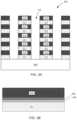
- FIGS. 1 A and 1 Bare schematic examples of material stacks that include a nucleation layer as a template for metal growth.
- FIGS. 2 , 3 A, and 3 Bprovide examples of structures in which the material stacks may be employed according to various embodiments.
- FIG. 4is a process flow diagram illustrating operations in a method of depositing a conductive material according to various embodiments
- FIG. 5shows atomic layer deposition growth rate on a dielectric surface of a molybdenum-containing layer using ammonia reducing agent and a molybdenum oxychloride precursor.
- FIG. 6shows molybdenum growth from hydrogen and a molybdenum oxychloride on a nucleation layer deposited on a dielectric surface as described compared to molybdenum growth from hydrogen and a molybdenum oxychloride directly on a dielectric surface.
- FIG. 7is a plot showing resistivity of molybdenum films deposited as described herein compared to a molybdenum film deposited on titanium nitride.
- FIG. 8is a block diagram of a processing system suitable for conducting deposition processes in accordance with embodiments described herein.
- low resistance metallization stack structuresfor logic and memory applications and related methods of fabrication.
- thin metal oxynitride or metal nitride nucleation layersare deposited followed by deposition of a pure metal conductor.
- the nucleation layeris amorphous, which templates large pure metal film grain growth and reduced resistivity. Further, certain embodiments of the methods described below convert most or all of the metal oxynitride nucleation layer to a pure metal layer, further lowering the resistivity.
- deposition of metals such as Mo directly on aluminum oxide and other dielectricsmay be performed. In some embodiments, these depositions may be performed at temperatures less than 500° C. or even lower than 400° C. without significant nucleation delay. Deposition at low temperatures can result in better step coverage. In various embodiments, lower resistivity films may be obtained from large grain size of the films and/or because the films may be deposited directly on dielectrics without high resistivity films such as titanium nitride (TiN). Addition of a low-temperature metal-nitride nucleation layer can enable subsequent pure metal deposition at temperatures less than 600° C. or even less than 500° C.
- TiNtitanium nitride
- metal (nitride)+pure-metal nucleation stacksuitable for semiconductor applications that have thermal budgets of less than 600° C. or 500° C. for wafer processing.
- Thisenables deposition of metals without a high resistivity layer such as TiN and at temperatures inaccessible for pure films; for example, temperatures for pure Mo ALD can exceed 600° C. when deposited directly on dielectrics.
- FIGS. 1 A and 1 Bare schematic examples of material stacks that include a nucleation layer as a template for metal growth.
- FIGS. 1 A and 1 Billustrate the order of materials in a particular stack and may be used with any appropriate architecture and application, as described further below with respect to FIGS. 2 , 3 A, and 3 B .
- a substrate 102has a nucleation layer 108 deposited thereon.
- the substrate 102may be a silicon or other semiconductor wafer, e.g., a 200-mm wafer, a 300-mm wafer, or a 450-mm wafer, including wafers having one or more layers of material, such as dielectric, conducting, or semi-conducting material deposited thereon.
- the methodsmay also be applied to form metallization stack structures on other substrates, such as glass, plastic, and the like.
- a dielectric layer 104is on the substrate 102 .
- the dielectric layer 104may be deposited directly on a semiconductor (e.g., Si) surface of the substrate 102 , or there may be any number of intervening layers.
- Examples of dielectric layersinclude doped and undoped silicon oxide, silicon nitride, and aluminum oxide layers, with specific examples including doped or undoped layers SiO 2 and Al 2 O 3 .
- a diffusion barrier layer 106is disposed between the nucleation layer 108 and the dielectric layer 104 .
- a metal layer 110is deposited on the nucleation layer 108 and is the main conductor (also referred to as a bulk conductor or bulk layer) of the structure with the nucleation layer 108 providing a template for metal growth.
- the nucleation layer 108is deposited as an amorphous film.
- an amorphous filmwhich has large grains, as a template for metal growth, metal having large grains and low resistivity can be formed.
- metal layersinclude tungsten (W) and molybdenum (Mo) layers.
- FIG. 1 Bshows another example of a material stack.
- the stackincludes the substrate 102 , dielectric layer 104 , with the nucleation layer 108 deposited directly on the dielectric layer 104 , without an intervening diffusion barrier layer.
- a metal layer 110is deposited on the nucleation layer 108 and is the main conductor of the structure.
- the nucleation layer 108may be deposited a metal oxynitride layer, e.g., a tungsten oxynitride or molybdenum oxynitride layer. However, during subsequent processing, in certain embodiments, all or most of the nucleation layer 108 may be converted to a pure metal. Accordingly, according to various embodiments, the nucleation layer 108 may or may not be the same composition as the pure metal layer 110 .
- the nucleation layer 108may be characterized by its amorphous character, with the pure metal layer 110 characterized by its large grain size.
- the metal of the metal oxynitride layeris the same as that of the pure metal conductor, e.g., a molybdenum oxynitride layer may be deposited as a nucleation layer prior to deposition of a molybdenum layer or a tungsten oxynitride layer may be deposited as a nucleation layer prior to deposition of a tungsten layer.
- the metal oxynitride layermay have a different metal than that of the pure conductor, e.g., a tungsten layer may be deposited on a molybdenum-containing nucleation layer or a molybdenum layer may be deposited on a tungsten-containing nucleation layer.
- the nucleation layermay be deposited directly on a Si or other semiconductor substrate as a template for metal growth.
- tungsten (W) or molybdenum (Mo) growth on the nucleation layersis described above, the nucleation layers may be serve as a template for low resistivity growth of other metals cobalt (Co), ruthenium (Ru), nickel (Ni), and alloys including these metals such as MoW.
- the nucleation layermay be any appropriate metal oxynitride or metal nitride layer, including molybdenum oxynitride, molybdenum nitride, tungsten oxynitride, tungsten nitride, nickel nitride, etc.
- FIG. 2depicts a schematic example of a DRAM architecture including a buried wordline (bWL) 210 in a silicon substrate 202 .
- the bWL 210is formed in a trench etched in the silicon substrate 202 . Lining the trench is a conformal nucleation layer 208 and an insulating layer 204 that is disposed between the conformal nucleation layer 208 and the silicon substrate 202 .
- bWLburied wordline
- the insulating layer 204may be a gate oxide layer, formed from a high-k dielectric material such as a silicon oxide or silicon nitride material.
- a conformal barrier layersuch as TiN or a tungsten-containing layer may be interposed between the nucleation layer 208 and the insulating layer 204 .
- FIG. 3 Adepicts a schematic example of wordlines 310 in a 3D NAND structure 323 .
- the wordlines 310are separated by oxide layers 311 .
- FIG. 3 Ba detail of the interface between a wordline 310 and oxide layer 311 is shown including a layer of aluminum oxide (Al 2 O 3 ) 304 and a nucleation layer 308 is shown.
- the nucleation layer 308may be deposited directly on the oxide layer 311 or on a TiN or other barrier layer as described herein.
- the nucleation layersmay be between about 10 A and 100 A, or 10 A and 50 A, for example, for deposition of a wordline 310 of between about 10 nm and 100 nm thick.
- the reducing agentis ammonia (NH 3 ) or other nitrogen-containing reducing agent such hydrazine (N 2 H 4 ).
- NH 3 chemisorption on dielectricsis more favorable than that of hydrogen (H 2 ).
- the reducing agent and precursorare selected such that they react without reducing agent dissociation.
- NH 3reacts with metal oxychlorides and metal chlorides without dissociation. This is in contrast to, for example, ALD from metal oxychlorides that uses H 2 as a reducing agent; H 2 dissociates on the surface to form adsorbed atomic hydrogen, which results in very low concentrations of reactive species and low surface coverage during initial nucleation of metal on the dielectric surface.
- the reducing agentmay be a boron-containing or silicon-containing reducing agent such as diborane (B 2 H 6 ) or (SiH 4 ).
- B 2 H 6diborane
- SiH 4silicon-containing reducing agent
- metal chloride precursorssuch as aluminum chloride
- metal oxychloridessuch as aluminum oxychlorides
- the B 2 H 6 and SiH 4will react with water formed as a byproduct during the ALD process and form solid B 2 O 3 and SiO 2 , which are insulating and will remain in the film, increasing resistivity.
- Use of NH 3also has improved adhesion over B 2 H 6 and SiH 4 ALD processes on certain surfaces including Al 2 O 3 .
- metal oxychloride and metal chloride precursorsexamples include molybdenum pentachloride (MoCl 5 ), molybdenum oxychlorides such as molybdenum dichloride dioxide (MoO 2 Cl 2 ) and molybdenum oxytetrachloride (MoOCl 4 ), tungsten pentachloride (WCl 5 ), tungsten hexachloride (WCl 6 ), tungsten tetrachloride (WCl 4 ), tungsten dichloride (WCl 2 ), and tungsten oxychlorides (WO x Cl y ) such as tungsten oxytetrachloride (WOCl 4 ).
- MoCl 5molybdenum pentachloride
- MoOCl 4molybdenum oxychlorides
- tungsten pentachloride (WCl 5 )tungsten hexachloride (WCl 6 )
- tungsten tetrachloride
- the metal chloride and metal oxychloridemay be useful in embodiments in which fluorine incorporation is a concern.
- fluorine-containing precursorsmay be used. These include metal fluorides such as tungsten hexafluoride (WF 6 ), molybdenum hexafluoride (MoF 6 ), and molybdenum pentafluoride (MoF 5 ).
- the nucleation layermay be converted to a pure (or less impure) elemental metal film with the thickness decreasing.
- Substrate temperature for nucleation layer depositionmay range, for example, from 300° C.-600° C. In some embodiments, low temperatures may be used. Such temperatures may be less than 500° C., less than 550° C., less than 450° C., less than 400° C., or less than 350° C. Low temperatures may be used for improved step coverage. In addition, low temperatures may increase the amount of impurities in the nucleation layer, increasing the amorphous character, which in turn may increase grain size of the subsequently deposited conductor.
- the surface on which the nucleation layer is depositeddepends on the particular application.
- the nucleation layeris deposited directly on a dielectric (e.g., silicon oxide, aluminum oxide, silicon nitride, etc.) surface.
- the nucleation layeris deposited directly on a titanium nitride or other surface.
- the subsequent elemental metal depositionmay be performed on any surface.
- the temperaturemay be the same temperature as used in operation 402 in some embodiments.
- the metal precursormay also be the same or a different precursor than in employed in operation 402 . In some embodiments, the same precursor is used, with only the reducing agent changed.
- operation 404may facilitate conversion of the metal nitride or metal oxynitride nucleation layer to an elemental metal film. According to various embodiments, operation 404 may or may not deposit an appreciable amount of film of the main conductor.
- the substrate temperatureis raised.
- operation 406is also performed.
- operation 406may be performed.
- the temperaturemay be raised in operation 406 to a higher temperature at which deposition of the main conductor will be performed.
- the temperaturemay be greater than 500° C., and in some embodiments, greater than 600° C.
- a lower temperaturee.g, between 400° C. and 500° C., endpoints inclusive
- the temperaturemay or may not be raised, depending on the temperature of previous operations.
- the methodmay then proceed to an operation 408 (from any of operation 402 , 404 , or 406 ) in which the main conductor is deposited by ALD.
- operation 404if performed, H 2 may be used as a reducing agent.
- metal oxychloride and metal chloride precursorsthat may be employed in operations 404 and 408 include molybdenum pentachloride (MoCl 5 ) and molybdenum hexachloride (MoCl 6 ), molybdenum oxychlorides such as molybdenum dichloride dioxide (MoO 2 Cl 2 ) and molybdenum oxytetrachloride (MoOCl 4 ), tungsten pentachloride (WCl 5 ), tungsten hexachloride (WCl 6 ), tungsten tetrachloride (WCl 4 ), tungsten dichloride (WCl 2 ), and tungsten oxychlorides (WO x Cl y ) such as tungsten oxytetrachloride (WOCl 4 ).
- MoCl 5molybdenum pentachloride
- MoCl 6molybdenum hexachloride
- MoOCl 4molybdenum
- the nucleation layeris converted to an elemental metal layer. This may also be characterized as removing impurities, i.e., any non-metal constituent.
- the nucleation layermay have greater impurities than the subsequently deposited elemental layer, but they are sufficiently removed such that the stack resistivity is the same or similar to a stack that does not include a nucleation layer.
- the thicknesswill also decrease; for example, a 30 A as-deposited film may contribute about 10 A metal to the stack.
- one or more of the followingmay be employed to facilitate conversion of the nucleation layer to an elemental metal film: 1) depositing the bulk conductor at a higher temperature (e.g., 550° C.) than the nucleation layer is deposited, 2) performing lower temperature ALD H 2 /metal precursor cycles as described with reference to operation 404 above, and 3) in-situ deposition of the bulk layer, such that the nucleation layer is not exposed to air or otherwise oxidized before bulk deposition.
- Mo oxychlorides and W oxychloridesin particular are relatively easy to convert to elemental metal.
- the resulting converted nucleation layer and pure metal layermay each be characterized as having fewer than 1% atomic impurities.
- FIG. 5shows results of forming a Mo-containing layer using NH 3 a reducing agent and a molybdenum oxychloride precursor to form a nucleation layer, then converting the Mo-containing layer to Mo as described above.
- FIG. 5shows the nucleation layer thickness, after conversion to Mo, is shown as a function of ALD cycles. At each temperature (350° C.—low, 400° C.—med, 450° C.—high), deposition was performed on three different surfaces: an Al 2 O 3 surface, a TiN surface, and a thermal SiO 2 surface. At each temperature, the growth rate is the same for all surfaces. Thus, while the growth rate is insensitive to temperature, it is insensitive to substrate surface.
- an H 2 and molybdenum oxychloride ALD depositionwould deposit on TiN, deposit a small amount on SiO 2 , and deposit almost nothing on Al 2 O 3 .
- FIG. 6shows subsequent Mo growth from H 2 and molybdenum oxychloride ALD cycles on a nucleation layer deposited on an Al 2 O 3 surface as described above as compared to Mo growth from H 2 and molybdenum oxychloride ALD cycles directly on an Al 2 O 3 surface at 550° C.
- Curve Ashows Mo growth on approximately 10
- curve Bshows Mo growth on Al 2 O 3 .
- ALD deposition from H 2 reduction of the Mo precursorshows a steady growth on the Mo nucleation layer deposited from NH 3 reduction of the Mo precursor, with no nucleation delay.
- the H 2 /Mo precursor ALD cyclesresult in no deposition on Al 2 O 3 .
- FIG. 7shows resistivity of various Mo films.
- Curve Arepresents resistivity of H 2 /Mo oxychloride ALD film on a low temperature NH 3 /Mo oxychloride nucleation layer
- Curve Brepresents resistivity of H 2 /Mo oxychloride ALD film on a high temperature NH 3 /Mo oxychloride nucleation layer
- Curve Crepresents resistivity of H 2 /Mo oxychloride ALD film on TiN. No increase in blanket resistivity is found using the nucleation layers described herein, indicating that they are converted to elemental Mo films.
- metal oxychloride and metal chloride precursorsWhile the description above refers to metal oxychloride and metal chloride precursors, the methods may also be performed with other halogen containing precursors including metal oxyfluoride and metal fluoride precursors.
- the methodsmay involve depositing a metal oxynitride or metal nitride nucleation layer followed by deposition of a pure metal layer by chemical vapor deposition (CVD).
- CVDchemical vapor deposition
- Example deposition apparatusesinclude various systems, e.g., ALTUS® and ALTUS® Max, available from Lam Research Corp., of Fremont, California, or any of a variety of other commercially available processing systems. The process can be performed on multiple deposition stations in parallel.
- a nucleation layer deposition processis performed at a first station that is one of two, five, or even more deposition stations positioned within a single deposition chamber.
- nucleation layer depositionmay be performed at a first station, followed by lower temperature hydrogen reduction of a metal precursor at a second station, followed by high temperature hydrogen reduction of a metal precursor at a third station.
- Each stationmay have independent temperature control.
- various steps for the processare performed at two different stations of a deposition chamber.
- multiple chambersare used to perform the methods described herein.
- deposition of the nucleation layermay be performed in a first chamber and deposition of the bulk metal layer performed in a second chamber.
- the two chambersmay be connected to a common vacuum chamber such that the substrate can be transferred between them without exposure.
- the chambersare not connected under vacuum, with the substrate exposed to air during transfer. Any oxidation can be reduced in the subsequent processing as described above.
- FIG. 8is a block diagram of a processing system suitable for conducting deposition processes in accordance with embodiments described herein.
- the system 800includes a transfer module 803 .
- the transfer module 803provides a clean, pressurized environment to minimize the risk of contamination of substrates being processed as they are moved between the various reactor modules.
- Mounted on the transfer module 803is a multi-station reactor 809 capable of performing ALD depositions as described herein.
- Chamber 809may include multiple stations 811 , 813 , 815 , and 817 that may sequentially perform these operations.
- chamber 809could be configured such that stations 811 and 813 perform nucleation layer deposition, and stations 813 and 815 perform bulk layer deposition.
- Each deposition stationmay include a heated wafer pedestal and a showerhead, dispersion plate or other gas inlet.
- the transfer module 803may be one or more single or multi-station modules 807 capable of performing plasma or chemical (non-plasma) pre-cleans.
- the modulemay also be used for various other treatments, e.g., reducing agent soaking.
- the system 800also includes one or more (in this case two) wafer source modules 801 where wafers are stored before and after processing.
- An atmospheric robot(not shown) in the atmospheric transfer chamber 819 first removes wafers from the source modules 801 to loadlocks 821 .
- a wafer transfer device(generally a robot arm unit) in the transfer module 1103 moves the wafers from loadlocks 821 to and among the modules mounted on the transfer module 803 .
- a high temperature showerheadis employed.
- NH 3 and metal oxychloride or metal chloride precursorscan be used in a single plenum showerhead without NH 4 Cl condensation.
- dual-plenum showerheadsmay be used in which NH 3 is delivered through one plenum and metal chloride or oxychloride precursors can be delivered through the other plenum.
- depositing both metal (nitride) nucleation and pure metal in a single process chamberfacilitates the conversion of the as-deposited metal+O x +NH x +Cl x nucleation film to pure metal by high-temperature reaction with Hz, metal (oxychloride), and their byproducts (HCl, OCl x , Metal-Cl x , . . . ). This may be done in a multi-station reactor with low-temperature at the first deposition station and high temperatures at subsequent deposition stations as described above.
- the individual deposition stations in a multi-station deposition reactorcan be isolated from each other by shaping the showerheads and pedestals such that in a pedestal-up process position, the two assemblies create a small process volume above the wafer and a very narrow gap to isolate the process volume from the main chamber.
- the narrow gap at the edge of the process volumecan be augmented with an inert gas purge barrier to make it difficult for gas to diffuse from the main chamber into the process volume.
- the narrow gap at the edge of the process volumecan also incorporate a local pumping plenum to prevent process gas from entering the main chamber. This can eliminate the risk of deposition or particle generation in the main chamber.
- the narrow edge gapby itself can eliminate the risk of gas from the main chamber diffusing back into the wafer processing volume such there is no station to station cross talk.
- a systemincludes two different deposition chambers.
- two deposition chambersmay be mounted on transfer module 803 .
- each deposition chambermay be a single or multi-station chamber.
- two deposition chambers not under common vacuummay be employed.
- a system controller 829is employed to control process conditions during deposition.
- the controllerwill typically include one or more memory devices and one or more processors.
- the processormay include a CPU or computer, analog and/or digital input/output connections, stepper motor controller boards, etc.
- the controllermay control all of the activities of the deposition apparatus.
- the system controllerexecutes system control software including sets of instructions for controlling the timing, mixture of gases, chamber pressure, chamber temperature, wafer temperature, radio frequency (RF) power levels if used, wafer chuck or pedestal position, and other parameters of a particular process.
- RFradio frequency
- Other computer programs stored on memory devices associated with the controllermay be employed in some embodiments.
- the user interfacemay include a display screen, graphical software displays of the apparatus and/or process conditions, and user input devices such as pointing devices, keyboards, touch screens, microphones, etc.
- System control logicmay be configured in any suitable way.
- the logiccan be designed or configured in hardware and/or software.
- the instructions for controlling the drive circuitrymay be hard coded or provided as software.
- the instructionsmay be provided by “programming” Such programming is understood to include logic of any form, including hard coded logic in digital signal processors, application-specific integrated circuits, and other devices which have specific algorithms implemented as hardware. Programming is also understood to include software or firmware instructions that may be executed on a general-purpose processor.
- System control softwaremay be coded in any suitable computer readable programming language. Alternatively, the control logic may be hard coded in the controller.
- Applications Specific Integrated Circuits, Programmable Logic Devicese.g., field-programmable gate arrays, or FPGAs
- functionally comparable hard coded logicmay be used in its place.
- the computer program code for controlling the deposition and other processes in a process sequencecan be written in any conventional computer readable programming language: for example, assembly language, C, C++, Pascal, Fortran or others. Compiled object code or script is executed by the processor to perform the tasks identified in the program.
- the controller parametersrelate to process conditions such as, for example, process gas composition and flow rates, temperature, pressure, cooling gas pressure, and chamber wall temperature. These parameters are provided to the user in the form of a recipe and may be entered utilizing the user interface.
- Signals for monitoring the processmay be provided by analog and/or digital input connections of the system controller.
- the signals for controlling the processare output on the analog and digital output connections of the deposition apparatus.
- the system softwaremay be designed or configured in many different ways. For example, various chamber component subroutines or control objects may be written to control operation of the chamber components necessary to carry out the deposition processes described herein. Examples of programs or sections of programs for this purpose include substrate positioning code, process gas control code, pressure control code, and heater control code.
- a controller 829is part of a system, which may be part of the above-described examples.
- Such systemscan include semiconductor processing equipment, including a processing tool or tools, chamber or chambers, a platform or platforms for processing, and/or specific processing components (a wafer pedestal, a gas flow system, etc.).
- These systemsmay be integrated with electronics for controlling their operation before, during, and after processing of a semiconductor wafer or substrate.
- the electronicsmay be referred to as the “controller,” which may control various components or subparts of the system or systems.
- the controllermay be defined as electronics having various integrated circuits, logic, memory, and/or software that receive instructions, issue instructions, control operation, enable cleaning operations, enable endpoint measurements, and the like.
- the integrated circuitsmay include chips in the form of firmware that store program instructions, digital signal processors (DSPs), chips defined as application specific integrated circuits (ASICs), and/or one or more microprocessors, or microcontrollers that execute program instructions (e.g., software).
- Program instructionsmay be instructions communicated to the controller in the form of various individual settings (or program files), defining operational parameters for carrying out a particular process on or for a semiconductor wafer or to a system.
- the operational parametersmay, in some embodiments, be part of a recipe defined by process engineers to accomplish one or more processing steps during the fabrication of one or more layers, materials, metals, oxides, silicon, silicon dioxide, surfaces, circuits, and/or dies of a wafer.
- the controller 829may be a part of or coupled to a computer that is integrated with, coupled to the system, otherwise networked to the system, or a combination thereof.
- the controller 829may be in the “cloud” or all or a part of a fab host computer system, which can allow for remote access of the wafer processing.
- the computermay enable remote access to the system to monitor current progress of fabrication operations, examine a history of past fabrication operations, examine trends or performance metrics from a plurality of fabrication operations, to change parameters of current processing, to set processing steps to follow a current processing, or to start a new process.
- a remote computere.g.
Landscapes
- Chemical & Material Sciences (AREA)
- Engineering & Computer Science (AREA)
- Chemical Kinetics & Catalysis (AREA)
- General Chemical & Material Sciences (AREA)
- Materials Engineering (AREA)
- Mechanical Engineering (AREA)
- Metallurgy (AREA)
- Organic Chemistry (AREA)
- General Physics & Mathematics (AREA)
- Condensed Matter Physics & Semiconductors (AREA)
- Physics & Mathematics (AREA)
- Manufacturing & Machinery (AREA)
- Computer Hardware Design (AREA)
- Microelectronics & Electronic Packaging (AREA)
- Power Engineering (AREA)
- Inorganic Chemistry (AREA)
- Crystallography & Structural Chemistry (AREA)
- Chemical Vapour Deposition (AREA)
- Electrodes Of Semiconductors (AREA)
- Semiconductor Memories (AREA)
- Internal Circuitry In Semiconductor Integrated Circuit Devices (AREA)
Abstract
Description
An Application Data Sheet is filed concurrently with this specification as part of the present application. Each application that the present application claims benefit of or priority to as identified in the concurrently filed Application Data Sheet is incorporated by reference herein in their entireties and for all purposes.
Tungsten (W) film deposition using chemical vapor deposition (CVD) techniques is an integral part of semiconductor fabrication processes. For example, tungsten films may be used as low resistivity electrical connections in the form of horizontal interconnects, vias between adjacent metal layers, and contacts between a first metal layer and the devices on a silicon substrate. Tungsten films may also be used in various memory applications, including in formation of buried wordline (bWL) architectures for dynamic random access memory (DRAM), word lines for 3D NAND, and logic applications. However, the continued decrease in feature size and film thickness brings various challenges including high resistivity for thinner films. Other metals such as molybdenum (Mo) are being evaluated as low resistivity replacements for W.
The background description provided herein is for the purposes of generally presenting the context of the disclosure. Work of the presently named inventors, to the extent it is described in this background section, as well as aspects of the description that may not otherwise qualify as prior art at the time of filing, are neither expressly nor impliedly admitted as prior art against the present disclosure.
One aspect of the disclosure relates to method of depositing metal. It includes depositing a first layer from a metal oxychloride precursor and ammonia using a first atomic layer deposition (ALD) process. It also includes depositing an elemental metal layer on the first layer from a metal oxychloride precursor and hydrogen using a second ALD process.
Implementations may include one or more of the following features. The method where the first layer is a metal oxynitride or metal nitride layer. The method where the first layer is converted to an elemental metal layer during or prior to the second ALD process. The method where the converted elemental metal later contains less than 1 (atomic) % impurities. The method where the first layer is an amorphous layer. The method where the elemental layer is crystalline. The method where the first and second ALD processes are performed in the same chamber and without exposure to air. The method where the first layer is a template for metal grain growth in the second layer. The method where the elemental layer contains less than 1 (atomic) % impurities. The method where the elemental metal layer is elemental tungsten. The method where the elemental metal layer is elemental molybdenum. The method where the first layer is one of molybdenum oxynitride and molybdenum nitride. The method where the first ALD process is performed at a temperature less than 400° C.
The method where the second ALD process is performed at a temperature greater than 400° C. The method where deposition of the first layer and deposition of the elemental layer are performed in the same chamber. The method where deposition of the first layer and deposition of the elemental layer are performed in different stations of the same chamber. The method where deposition of the first layer is performed in a first chamber and deposition of the elemental layer is performed in a second chamber. The method further including exposing the first layer to a prior to deposition of the elemental layer.
Another aspect of the disclosure includes relates to an apparatus including: first and second process chambers each configured to house a substrate, a substrate support in each of the process chambers, gas inlets configured to direct gas into each of the process chambers, a heater configured to heat the substrate support in each process chamber, and a controller including program instructions for:. The apparatus also includes sequentially inletting a metal oxychloride precursor and ammonia into the first process chamber while a substrate is housed in the first process chamber. The apparatus also includes after (a), transfer the substrate to the second process chamber. The apparatus also includes after (b), sequentially inletting a metal oxychloride precursor and hydrogen into the second process chamber while the substrate is housed in the second process chamber.
Another aspect of the disclosure relates to an apparatus including: a process chamber having one or more stations, each configured to house a substrate; a substrate support in each of the one or more stations; gas inlets configured to direct gas into each of the one or more stations; a heater configured to heat the substrate support in each station; and a controller including program instructions for: sequentially inletting a metal oxychloride precursor and ammonia into one of the one or stations; and sequentially inletting a metal oxychloride precursor and hydrogen into one of the one or stations.
These and other aspects are described more fully below with reference to the drawings.
In the following description, numerous specific details are set forth to provide a thorough understanding of the presented embodiments. The disclosed embodiments may be practiced without some or all of these specific details. In other instances, well-known process operations have not been described in detail to not unnecessarily obscure the disclosed embodiments. While the disclosed embodiments will be described in conjunction with the specific embodiments, it will be understood that it is not intended to limit the disclosed embodiments.
Provided herein are low resistance metallization stack structures for logic and memory applications and related methods of fabrication. In some embodiments, thin metal oxynitride or metal nitride nucleation layers are deposited followed by deposition of a pure metal conductor. The nucleation layer is amorphous, which templates large pure metal film grain growth and reduced resistivity. Further, certain embodiments of the methods described below convert most or all of the metal oxynitride nucleation layer to a pure metal layer, further lowering the resistivity.
According to various embodiments, one or more advantages may be realized. In some embodiments, deposition of metals such as Mo directly on aluminum oxide and other dielectrics may be performed. In some embodiments, these depositions may be performed at temperatures less than 500° C. or even lower than 400° C. without significant nucleation delay. Deposition at low temperatures can result in better step coverage. In various embodiments, lower resistivity films may be obtained from large grain size of the films and/or because the films may be deposited directly on dielectrics without high resistivity films such as titanium nitride (TiN). Addition of a low-temperature metal-nitride nucleation layer can enable subsequent pure metal deposition at temperatures less than 600° C. or even less than 500° C. This can make the metal (nitride)+pure-metal nucleation stack suitable for semiconductor applications that have thermal budgets of less than 600° C. or 500° C. for wafer processing. This enables deposition of metals without a high resistivity layer such as TiN and at temperatures inaccessible for pure films; for example, temperatures for pure Mo ALD can exceed 600° C. when deposited directly on dielectrics.
InFIG.1A , adielectric layer 104 is on thesubstrate 102. Thedielectric layer 104 may be deposited directly on a semiconductor (e.g., Si) surface of thesubstrate 102, or there may be any number of intervening layers. Examples of dielectric layers include doped and undoped silicon oxide, silicon nitride, and aluminum oxide layers, with specific examples including doped or undoped layers SiO2and Al2O3. Also, inFIG.1A , adiffusion barrier layer 106 is disposed between thenucleation layer 108 and thedielectric layer 104. Examples of diffusion barrier layers including titanium nitride (TiN), titanium/titanium nitride (Ti/TiN), tungsten nitride (WN), and tungsten carbon nitride (WCN). Ametal layer 110 is deposited on thenucleation layer 108 and is the main conductor (also referred to as a bulk conductor or bulk layer) of the structure with thenucleation layer 108 providing a template for metal growth.
As described further below, thenucleation layer 108 is deposited as an amorphous film. By using an amorphous film, which has large grains, as a template for metal growth, metal having large grains and low resistivity can be formed. Examples of metal layers include tungsten (W) and molybdenum (Mo) layers.
In the examples ofFIGS.1A and1B , thenucleation layer 108 may be deposited a metal oxynitride layer, e.g., a tungsten oxynitride or molybdenum oxynitride layer. However, during subsequent processing, in certain embodiments, all or most of thenucleation layer 108 may be converted to a pure metal. Accordingly, according to various embodiments, thenucleation layer 108 may or may not be the same composition as thepure metal layer 110. Thenucleation layer 108 may be characterized by its amorphous character, with thepure metal layer 110 characterized by its large grain size.
In some embodiments, the metal of the metal oxynitride layer is the same as that of the pure metal conductor, e.g., a molybdenum oxynitride layer may be deposited as a nucleation layer prior to deposition of a molybdenum layer or a tungsten oxynitride layer may be deposited as a nucleation layer prior to deposition of a tungsten layer. In other embodiments, the metal oxynitride layer may have a different metal than that of the pure conductor, e.g., a tungsten layer may be deposited on a molybdenum-containing nucleation layer or a molybdenum layer may be deposited on a tungsten-containing nucleation layer.
WhileFIGS.1A and1B show examples of metallization stacks, the methods and resulting stacks are not so limited. For example, in some embodiments, the nucleation layer may be deposited directly on a Si or other semiconductor substrate as a template for metal growth. Further, while tungsten (W) or molybdenum (Mo) growth on the nucleation layers is described above, the nucleation layers may be serve as a template for low resistivity growth of other metals cobalt (Co), ruthenium (Ru), nickel (Ni), and alloys including these metals such as MoW. Still further, the nucleation layer may be any appropriate metal oxynitride or metal nitride layer, including molybdenum oxynitride, molybdenum nitride, tungsten oxynitride, tungsten nitride, nickel nitride, etc.
The material stacks described above and further below may be implemented in a variety of structures.FIGS.2,3A, and3B provide examples of structures in which the stacks may be employed.FIG.2 depicts a schematic example of a DRAM architecture including a buried wordline (bWL)210 in asilicon substrate 202. ThebWL 210 is formed in a trench etched in thesilicon substrate 202. Lining the trench is aconformal nucleation layer 208 and an insulatinglayer 204 that is disposed between theconformal nucleation layer 208 and thesilicon substrate 202. In the example ofFIG.2 , the insulatinglayer 204 may be a gate oxide layer, formed from a high-k dielectric material such as a silicon oxide or silicon nitride material. In some embodiments, a conformal barrier layer such as TiN or a tungsten-containing layer may be interposed between thenucleation layer 208 and the insulatinglayer 204.
In some embodiments, the reducing agent is ammonia (NH3) or other nitrogen-containing reducing agent such hydrazine (N2H4). NH3chemisorption on dielectrics is more favorable than that of hydrogen (H2). In some embodiments, the reducing agent and precursor are selected such that they react without reducing agent dissociation. NH3reacts with metal oxychlorides and metal chlorides without dissociation. This is in contrast to, for example, ALD from metal oxychlorides that uses H2as a reducing agent; H2dissociates on the surface to form adsorbed atomic hydrogen, which results in very low concentrations of reactive species and low surface coverage during initial nucleation of metal on the dielectric surface. By using NH3and metal oxychloride or metal chloride precursors, nucleation delay is reduced or eliminated at deposition temperatures up to hundreds of degrees lower than used by H2reduction of the same metal precursors.
In some embodiments, the reducing agent may be a boron-containing or silicon-containing reducing agent such as diborane (B2H6) or (SiH4). These reducing agents may be used with metal chloride precursors; with metal oxychlorides, however, the B2H6and SiH4will react with water formed as a byproduct during the ALD process and form solid B2O3and SiO2, which are insulating and will remain in the film, increasing resistivity. Use of NH3also has improved adhesion over B2H6and SiH4ALD processes on certain surfaces including Al2O3.
Examples of metal oxychloride and metal chloride precursors include molybdenum pentachloride (MoCl5), molybdenum oxychlorides such as molybdenum dichloride dioxide (MoO2Cl2) and molybdenum oxytetrachloride (MoOCl4), tungsten pentachloride (WCl5), tungsten hexachloride (WCl6), tungsten tetrachloride (WCl4), tungsten dichloride (WCl2), and tungsten oxychlorides (WOxCly) such as tungsten oxytetrachloride (WOCl4).
The metal chloride and metal oxychloride may be useful in embodiments in which fluorine incorporation is a concern. However, in some embodiments, fluorine-containing precursors may be used. These include metal fluorides such as tungsten hexafluoride (WF6), molybdenum hexafluoride (MoF6), and molybdenum pentafluoride (MoF5).
The resulting nucleation layer is generally not a pure elemental film but a metal nitride or metal oxynitride film. In some embodiments, there may be residual chlorine or fluorine from the deposition, particularly if the deposition is performed at low temperatures. In some embodiments, there no more than a trace amount of residual chlorine or fluorine. In some embodiments, the nucleation layer is an amorphous layer. Impurities in the film (e.g., oxygen, NH3, chlorine or other halogen) facilitate growth of an amorphous microstructure. In some embodiments, the nucleation layer as deposited is an amorphous metal oxynitride layer or an amorphous metal nitride layer. The amorphous character templates large grain growth in the subsequently deposited conductor. The surface energy of nitride or oxynitride relative to an oxide surface is much more favorable than that of a metal on an oxide surface, facilitating formation of a continuous and smooth film on the dielectric. This allows formation of thin, continuous layers. Example thicknesses of the nucleation layer range from5-30A as deposited. Depending on the temperature, this may be about 5-50 ALD cycles for example.
As described below, during subsequent processing the nucleation layer may be converted to a pure (or less impure) elemental metal film with the thickness decreasing.
Substrate temperature for nucleation layer deposition may range, for example, from 300° C.-600° C. In some embodiments, low temperatures may be used. Such temperatures may be less than 500° C., less than 550° C., less than 450° C., less than 400° C., or less than 350° C. Low temperatures may be used for improved step coverage. In addition, low temperatures may increase the amount of impurities in the nucleation layer, increasing the amorphous character, which in turn may increase grain size of the subsequently deposited conductor.
The surface on which the nucleation layer is deposited depends on the particular application. In some embodiments, the nucleation layer is deposited directly on a dielectric (e.g., silicon oxide, aluminum oxide, silicon nitride, etc.) surface. In some embodiments, the nucleation layer is deposited directly on a titanium nitride or other surface. As discussed further below, by performingoperation 402, the subsequent elemental metal deposition may be performed on any surface.
After deposition of the nucleation layer, anoptional operation 404 may be performed. Inoperation 404, lower temperature ALD cycles a metal conductor and a reducing agent are performed. The “lower” temperature refers to the temperature inoperation 404, if performed, being lower than thesubsequent operation 406. Example temperatures may be less than 500° C., less than 550° C., less than 450° C., less than 400° C., or less than 350° C. In this operation, the reducing agent is different than inoperation 402, and in particular examples may be hydrogen (H2). In particular, H2may result in deposition of an elemental film with significantly fewer impurities than in the nucleation layer. The temperature may be the same temperature as used inoperation 402 in some embodiments. The metal precursor may also be the same or a different precursor than in employed inoperation 402. In some embodiments, the same precursor is used, with only the reducing agent changed. In some embodiments,operation 404 may facilitate conversion of the metal nitride or metal oxynitride nucleation layer to an elemental metal film. According to various embodiments,operation 404 may or may not deposit an appreciable amount of film of the main conductor.
In a furtheroptional operation 406, the substrate temperature is raised. In embodiments, in whichoperation 404 is performed,operation 406 is also performed. In other embodiments,operation 406 may be performed. For example, if the nucleation layer deposition occurs at relatively low temperatures (e.g., below 400° C.), the temperature may be raised inoperation 406 to a higher temperature at which deposition of the main conductor will be performed. In some embodiments, the temperature may be greater than 500° C., and in some embodiments, greater than 600° C. In some embodiments, a lower temperature (e.g, between 400° C. and 500° C., endpoints inclusive) may be used for bulk deposition. The temperature may or may not be raised, depending on the temperature of previous operations.
The method may then proceed to an operation408 (from any ofoperation
Examples of metal oxychloride and metal chloride precursors that may be employed inoperations
During one or more of operations404-408, the nucleation layer is converted to an elemental metal layer. This may also be characterized as removing impurities, i.e., any non-metal constituent. The nucleation layer may have greater impurities than the subsequently deposited elemental layer, but they are sufficiently removed such that the stack resistivity is the same or similar to a stack that does not include a nucleation layer. The thickness will also decrease; for example, a30A as-deposited film may contribute about10A metal to the stack.
According to various embodiments, one or more of the following may be employed to facilitate conversion of the nucleation layer to an elemental metal film: 1) depositing the bulk conductor at a higher temperature (e.g., 550° C.) than the nucleation layer is deposited, 2) performing lower temperature ALD H2/metal precursor cycles as described with reference tooperation 404 above, and 3) in-situ deposition of the bulk layer, such that the nucleation layer is not exposed to air or otherwise oxidized before bulk deposition. Mo oxychlorides and W oxychlorides in particular are relatively easy to convert to elemental metal. The resulting converted nucleation layer and pure metal layer may each be characterized as having fewer than 1% atomic impurities.
While the description above refers to metal oxychloride and metal chloride precursors, the methods may also be performed with other halogen containing precursors including metal oxyfluoride and metal fluoride precursors.
In some embodiments, the methods may involve depositing a metal oxynitride or metal nitride nucleation layer followed by deposition of a pure metal layer by chemical vapor deposition (CVD).
Apparatus
Any suitable chamber may be used to implement the disclosed embodiments. Example deposition apparatuses include various systems, e.g., ALTUS® and ALTUS® Max, available from Lam Research Corp., of Fremont, California, or any of a variety of other commercially available processing systems. The process can be performed on multiple deposition stations in parallel.
In some embodiments, a nucleation layer deposition process is performed at a first station that is one of two, five, or even more deposition stations positioned within a single deposition chamber. For example, nucleation layer deposition may be performed at a first station, followed by lower temperature hydrogen reduction of a metal precursor at a second station, followed by high temperature hydrogen reduction of a metal precursor at a third station. Each station may have independent temperature control. In some embodiments, various steps for the process are performed at two different stations of a deposition chamber. For example, the substrate may be exposed to NH3in a first station using an individual gas supply system that creates a localized atmosphere at the substrate surface, and then the substrate may be transferred to a second station to be exposed to a metal chloride, metal fluoride, or metal oxychloride precursor precursor to deposit the nucleation layer. In some embodiments, the substrate may then be transferred back to the first station for a second exposure of NH3. Then the substrate may be transferred to the second station for exposure to the metal precursor. The substrate may also be exposed to NH3at another station following the first metal chloride or metal oxychloride deposition. This may be repeated as necessary to complete nucleation layer deposition and proceed with bulk layer deposition in the same or different stations.
In some embodiments, multiple chambers are used to perform the methods described herein. For example, deposition of the nucleation layer may be performed in a first chamber and deposition of the bulk metal layer performed in a second chamber. The two chambers may be connected to a common vacuum chamber such that the substrate can be transferred between them without exposure. In alternate embodiments, the chambers are not connected under vacuum, with the substrate exposed to air during transfer. Any oxidation can be reduced in the subsequent processing as described above.
Also mounted on thetransfer module 803 may be one or more single ormulti-station modules 807 capable of performing plasma or chemical (non-plasma) pre-cleans. The module may also be used for various other treatments, e.g., reducing agent soaking. Thesystem 800 also includes one or more (in this case two)wafer source modules 801 where wafers are stored before and after processing. An atmospheric robot (not shown) in theatmospheric transfer chamber 819 first removes wafers from thesource modules 801 toloadlocks 821. A wafer transfer device (generally a robot arm unit) in the transfer module1103 moves the wafers fromloadlocks 821 to and among the modules mounted on thetransfer module 803.
In some embodiments, a high temperature showerhead is employed.
This allows single, rather than dual, plenum showerheads to be used. By maintaining showerhead internal wetted surfaces at greater than 150° C. or 200° C., NH3and metal oxychloride or metal chloride precursors can be used in a single plenum showerhead without NH4Cl condensation. Alternately dual-plenum showerheads may be used in which NH3is delivered through one plenum and metal chloride or oxychloride precursors can be delivered through the other plenum.
As noted above, in some embodiments, depositing both metal (nitride) nucleation and pure metal in a single process chamber facilitates the conversion of the as-deposited metal+Ox+NHx+Clxnucleation film to pure metal by high-temperature reaction with Hz, metal (oxychloride), and their byproducts (HCl, OClx, Metal-Clx, . . . ). This may be done in a multi-station reactor with low-temperature at the first deposition station and high temperatures at subsequent deposition stations as described above. In some embodiments, the individual deposition stations in a multi-station deposition reactor can be isolated from each other by shaping the showerheads and pedestals such that in a pedestal-up process position, the two assemblies create a small process volume above the wafer and a very narrow gap to isolate the process volume from the main chamber. The narrow gap at the edge of the process volume can be augmented with an inert gas purge barrier to make it difficult for gas to diffuse from the main chamber into the process volume. The narrow gap at the edge of the process volume can also incorporate a local pumping plenum to prevent process gas from entering the main chamber. This can eliminate the risk of deposition or particle generation in the main chamber. The narrow edge gap by itself can eliminate the risk of gas from the main chamber diffusing back into the wafer processing volume such there is no station to station cross talk.
As noted above, in certain embodiments, a system includes two different deposition chambers. For example, referring toFIG.8 , two deposition chambers may be mounted ontransfer module 803. In such embodiments, each deposition chamber may be a single or multi-station chamber. Still further, two deposition chambers not under common vacuum may be employed.
In certain embodiments, asystem controller 829 is employed to control process conditions during deposition. The controller will typically include one or more memory devices and one or more processors. The processor may include a CPU or computer, analog and/or digital input/output connections, stepper motor controller boards, etc.
The controller may control all of the activities of the deposition apparatus. The system controller executes system control software including sets of instructions for controlling the timing, mixture of gases, chamber pressure, chamber temperature, wafer temperature, radio frequency (RF) power levels if used, wafer chuck or pedestal position, and other parameters of a particular process. Other computer programs stored on memory devices associated with the controller may be employed in some embodiments.
Typically, there will be a user interface associated with the controller. The user interface may include a display screen, graphical software displays of the apparatus and/or process conditions, and user input devices such as pointing devices, keyboards, touch screens, microphones, etc.
System control logic may be configured in any suitable way. In general, the logic can be designed or configured in hardware and/or software. The instructions for controlling the drive circuitry may be hard coded or provided as software. The instructions may be provided by “programming” Such programming is understood to include logic of any form, including hard coded logic in digital signal processors, application-specific integrated circuits, and other devices which have specific algorithms implemented as hardware. Programming is also understood to include software or firmware instructions that may be executed on a general-purpose processor. System control software may be coded in any suitable computer readable programming language. Alternatively, the control logic may be hard coded in the controller. Applications Specific Integrated Circuits, Programmable Logic Devices (e.g., field-programmable gate arrays, or FPGAs) and the like may be used for these purposes. In the following discussion, wherever “software” or “code” is used, functionally comparable hard coded logic may be used in its place.
The computer program code for controlling the deposition and other processes in a process sequence can be written in any conventional computer readable programming language: for example, assembly language, C, C++, Pascal, Fortran or others. Compiled object code or script is executed by the processor to perform the tasks identified in the program.
The controller parameters relate to process conditions such as, for example, process gas composition and flow rates, temperature, pressure, cooling gas pressure, and chamber wall temperature. These parameters are provided to the user in the form of a recipe and may be entered utilizing the user interface.
Signals for monitoring the process may be provided by analog and/or digital input connections of the system controller. The signals for controlling the process are output on the analog and digital output connections of the deposition apparatus.
The system software may be designed or configured in many different ways. For example, various chamber component subroutines or control objects may be written to control operation of the chamber components necessary to carry out the deposition processes described herein. Examples of programs or sections of programs for this purpose include substrate positioning code, process gas control code, pressure control code, and heater control code.
In some implementations, acontroller 829 is part of a system, which may be part of the above-described examples. Such systems can include semiconductor processing equipment, including a processing tool or tools, chamber or chambers, a platform or platforms for processing, and/or specific processing components (a wafer pedestal, a gas flow system, etc.). These systems may be integrated with electronics for controlling their operation before, during, and after processing of a semiconductor wafer or substrate. The electronics may be referred to as the “controller,” which may control various components or subparts of the system or systems. Thecontroller 829, depending on the processing requirements and/or the type of system, may be programmed to control any of the processes disclosed herein, including the delivery of processing gases, temperature settings (e.g., heating and/or cooling), pressure settings, vacuum settings, power settings, radio frequency (RF) generator settings in some systems, RF matching circuit settings, frequency settings, flow rate settings, fluid delivery settings, positional and operation settings, wafer transfers into and out of a tool and other transfer tools and/or load locks connected to or interfaced with a specific system.
Broadly speaking, the controller may be defined as electronics having various integrated circuits, logic, memory, and/or software that receive instructions, issue instructions, control operation, enable cleaning operations, enable endpoint measurements, and the like. The integrated circuits may include chips in the form of firmware that store program instructions, digital signal processors (DSPs), chips defined as application specific integrated circuits (ASICs), and/or one or more microprocessors, or microcontrollers that execute program instructions (e.g., software). Program instructions may be instructions communicated to the controller in the form of various individual settings (or program files), defining operational parameters for carrying out a particular process on or for a semiconductor wafer or to a system. The operational parameters may, in some embodiments, be part of a recipe defined by process engineers to accomplish one or more processing steps during the fabrication of one or more layers, materials, metals, oxides, silicon, silicon dioxide, surfaces, circuits, and/or dies of a wafer.
Thecontroller 829, in some implementations, may be a part of or coupled to a computer that is integrated with, coupled to the system, otherwise networked to the system, or a combination thereof. For example, thecontroller 829 may be in the “cloud” or all or a part of a fab host computer system, which can allow for remote access of the wafer processing. The computer may enable remote access to the system to monitor current progress of fabrication operations, examine a history of past fabrication operations, examine trends or performance metrics from a plurality of fabrication operations, to change parameters of current processing, to set processing steps to follow a current processing, or to start a new process. In some examples, a remote computer (e.g. a server) can provide process recipes to a system over a network, which may include a local network or the Internet. The remote computer may include a user interface that enables entry or programming of parameters and/or settings, which are then communicated to the system from the remote computer. In some examples, the controller receives instructions in the form of data, which specify parameters for each of the processing steps to be performed during one or more operations. It should be understood that the parameters may be specific to the type of process to be performed and the type of tool that the controller is configured to interface with or control. Thus, as described above, the controller may be distributed, such as by including one or more discrete controllers that are networked together and working towards a common purpose, such as the processes and controls described herein. An example of a distributed controller for such purposes would be one or more integrated circuits on a chamber in communication with one or more integrated circuits located remotely (such as at the platform level or as part of a remote computer) that combine to control a process on the chamber.
Without limitation, example systems may include a plasma etch chamber or module, a deposition chamber or module, a spin-rinse chamber or module, a metal plating chamber or module, a clean chamber or module, a bevel edge etch chamber or module, a physical vapor deposition (PVD) chamber or module, a CVD chamber or module, an ALD chamber or module, an atomic layer etch (ALE) chamber or module, an ion implantation chamber or module, a track chamber or module, and any other semiconductor processing systems that may be associated or used in the fabrication and/or manufacturing of semiconductor wafers.
As noted above, depending on the process step or steps to be performed by the tool, the controller might communicate with one or more of other tool circuits or modules, other tool components, cluster tools, other tool interfaces, adjacent tools, neighboring tools, tools located throughout a factory, a main computer, another controller, or tools used in material transport that bring containers of wafers to and from tool locations and/or load ports in a semiconductor manufacturing factory.
Thecontroller 829 may include various programs. A substrate positioning program may include program code for controlling chamber components that are used to load the substrate onto a pedestal or chuck and to control the spacing between the substrate and other parts of the chamber such as a gas inlet and/or target. A process gas control program may include code for controlling gas composition and flow rates and optionally for flowing gas into the chamber prior to deposition in order to stabilize the pressure in the chamber. A pressure control program may include code for controlling the pressure in the chamber by regulating, e.g., a throttle valve in the exhaust system of the chamber. A heater control program may include code for controlling the current to a heating unit that is used to heat the substrate. Alternatively, the heater control program may control delivery of a heat transfer gas such as helium to the wafer chuck.
Examples of chamber sensors that may be monitored during deposition include mass flow controllers, pressure sensors such as manometers, and thermocouples located in pedestal or chuck. Appropriately programmed feedback and control algorithms may be used with data from these sensors to maintain desired process conditions.
The foregoing describes implementation of embodiments of the disclosure in a single or multi-chamber semiconductor processing tool.
The foregoing describes implementation of disclosed embodiments in a single or multi-chamber semiconductor processing tool. The apparatus and process described herein may be used in conjunction with lithographic patterning tools or processes, for example, for the fabrication or manufacture of semiconductor devices, displays, LEDs, photovoltaic panels, and the like. Typically, though not necessarily, such tools/processes will be used or conducted together in a common fabrication facility. Lithographic patterning of a film typically comprises some or all of the following steps, each step provided with a number of possible tools: (1) application of photoresist on a workpiece, i.e., substrate, using a spin-on or spray-on tool; (2) curing of photoresist using a hot plate or furnace or UV curing tool; (3) exposing the photoresist to visible or UV or x-ray light with a tool such as a wafer stepper; (4) developing the resist so as to selectively remove resist and thereby pattern it using a tool such as a wet bench; (5) transferring the resist pattern into an underlying film or workpiece by using a dry or plasma-assisted etching tool; and (6) removing the resist using a tool such as an RF or microwave plasma resist stripper.
In the description above and in the claims, numerical ranges are inclusive of the end points of the range. For example, “a thickness between 1 and 5 nm” includes 1 nm and 5 nm. Similarly, ranges represented by a dash are inclusive of the end points of the ranges.
Although the foregoing embodiments have been described in some detail for purposes of clarity of understanding, it will be apparent that certain changes and modifications may be practiced within the scope of the appended claims. It should be noted that there are many alternative ways of implementing the processes, systems, and apparatus of the present embodiments. Accordingly, the present embodiments are to be considered as illustrative and not restrictive, and the embodiments are not to be limited to the details given herein.
Claims (16)
1. A method comprising:
forming a nucleation layer having a first thickness by exposing a substrate in a reaction chamber to a molybdenum-containing precursor and a first reducing agent, wherein the molybdenum-containing precursor is a molybdenum oxychloride or a molybdenum chloride, wherein the first reducing agent comprises a boron-containing reducing agent, and wherein the molybdenum-containing precursor reacts with the boron-containing reducing agent to form the nucleation layer having the first thickness; and
forming a bulk layer by exposing the nucleation layer having the first thickness to a molybdenum oxychloride and a hydrogen (H2) reducing agent.
2. The method ofclaim 1 , wherein the molybdenum-containing precursor is a molybdenum oxychloride.
3. The method ofclaim 2 , wherein the molybdenum-containing precursor is molybdenum dichloride dioxide (MoO2Cl2).
4. The method ofclaim 1 , wherein the nucleation layer is formed using atomic layer deposition (ALD).
5. The method ofclaim 1 , wherein the bulk layer is formed by chemical vapor deposition (CVD).
6. The method ofclaim 1 , wherein the first reducing agent is a borane.
7. The method ofclaim 1 , wherein the molybdenum oxychloride used in forming the bulk layer is molybdenum dichloride dioxide (MoO2Cl2).
8. The method ofclaim 1 , wherein the bulk layer has a higher purity than the nucleation layer.
9. A method comprising:
forming an elemental nucleation layer on a substrate, wherein forming the elemental nucleation layer comprises reacting a molybdenum-containing precursor with a first reducing agent, wherein the molybdenum-containing precursor comprises at least one of a molybdenum oxychloride or a molybdenum chloride and wherein the first reducing agent comprises at least one of a silicon-containing reducing agent, a boron-containing reducing agent, or a nitrogen-containing reducing agent; and
forming a bulk layer by exposing the substrate to a molybdenum oxychloride and a hydrogen (H2) reducing agent.
10. The method ofclaim 9 , wherein the molybdenum-containing precursor is molybdenum dichloride dioxide (MoO2Cl2).
11. The method ofclaim 9 , wherein the elemental nucleation layer is formed using atomic layer deposition (ALD).
12. The method ofclaim 9 , wherein the bulk layer is formed by chemical vapor deposition (CVD).
13. The method ofclaim 9 , wherein the molybdenum oxychloride used in forming the bulk layer is molybdenum dichloride dioxide (MoO2Cl2).
14. The method ofclaim 9 , wherein the first reducing agent comprises a silicon-reducing agent.
15. The method ofclaim 9 , wherein the first reducing agent comprises a nitrogen-reducing agent.
16. The method ofclaim 9 , wherein the first reducing agent comprises a boron-reducing agent.
Priority Applications (1)
| Application Number | Priority Date | Filing Date | Title |
|---|---|---|---|
| US17/814,206US12351914B2 (en) | 2019-01-28 | 2022-07-21 | Deposition of films using molybdenum precursors |
Applications Claiming Priority (4)
| Application Number | Priority Date | Filing Date | Title |
|---|---|---|---|
| US201962797860P | 2019-01-28 | 2019-01-28 | |
| PCT/US2020/015241WO2020159882A1 (en) | 2019-01-28 | 2020-01-27 | Deposition of metal films |
| US202117310293A | 2021-07-27 | 2021-07-27 | |
| US17/814,206US12351914B2 (en) | 2019-01-28 | 2022-07-21 | Deposition of films using molybdenum precursors |
Related Parent Applications (2)
| Application Number | Title | Priority Date | Filing Date |
|---|---|---|---|
| US17/310,293ContinuationUS11970776B2 (en) | 2019-01-28 | 2020-01-27 | Atomic layer deposition of metal films |
| PCT/US2020/015241ContinuationWO2020159882A1 (en) | 2019-01-28 | 2020-01-27 | Deposition of metal films |
Publications (2)
| Publication Number | Publication Date |
|---|---|
| US20220356579A1 US20220356579A1 (en) | 2022-11-10 |
| US12351914B2true US12351914B2 (en) | 2025-07-08 |
Family
ID=71840093
Family Applications (3)
| Application Number | Title | Priority Date | Filing Date |
|---|---|---|---|
| US17/310,293Active2040-09-06US11970776B2 (en) | 2019-01-28 | 2020-01-27 | Atomic layer deposition of metal films |
| US17/814,206ActiveUS12351914B2 (en) | 2019-01-28 | 2022-07-21 | Deposition of films using molybdenum precursors |
| US18/626,278PendingUS20240271281A1 (en) | 2019-01-28 | 2024-04-03 | Deposition of metal films |
Family Applications Before (1)
| Application Number | Title | Priority Date | Filing Date |
|---|---|---|---|
| US17/310,293Active2040-09-06US11970776B2 (en) | 2019-01-28 | 2020-01-27 | Atomic layer deposition of metal films |
Family Applications After (1)
| Application Number | Title | Priority Date | Filing Date |
|---|---|---|---|
| US18/626,278PendingUS20240271281A1 (en) | 2019-01-28 | 2024-04-03 | Deposition of metal films |
Country Status (7)
| Country | Link |
|---|---|
| US (3) | US11970776B2 (en) |
| JP (3) | JP7581213B2 (en) |
| KR (2) | KR20220139417A (en) |
| CN (2) | CN113366144B (en) |
| SG (1) | SG11202108217UA (en) |
| TW (1) | TWI870380B (en) |
| WO (1) | WO2020159882A1 (en) |
Families Citing this family (10)
| Publication number | Priority date | Publication date | Assignee | Title |
|---|---|---|---|---|
| US10573522B2 (en) | 2016-08-16 | 2020-02-25 | Lam Research Corporation | Method for preventing line bending during metal fill process |
| KR102806630B1 (en) | 2018-05-03 | 2025-05-12 | 램 리써치 코포레이션 | Method for depositing tungsten and other metals on 3D NAND structures |
| US12148623B2 (en) | 2018-11-19 | 2024-11-19 | Lam Research Corporation | Deposition of tungsten on molybdenum templates |
| CN113366144B (en)* | 2019-01-28 | 2023-07-07 | 朗姆研究公司 | Deposition of metal films |
| SG11202109796QA (en) | 2019-03-11 | 2021-10-28 | Lam Res Corp | Precursors for deposition of molybdenum-containing films |
| WO2021046058A1 (en) | 2019-09-03 | 2021-03-11 | Lam Research Corporation | Molybdenum deposition |
| US12327762B2 (en) | 2019-10-15 | 2025-06-10 | Lam Research Corporation | Molybdenum fill |
| WO2022221210A1 (en)* | 2021-04-14 | 2022-10-20 | Lam Research Corporation | Deposition of molybdenum |
| TW202411448A (en)* | 2022-05-02 | 2024-03-16 | 荷蘭商Asm Ip私人控股有限公司 | Method of forming structure including a doped adhesion film |
| CN115261821A (en)* | 2022-08-08 | 2022-11-01 | 中国科学院上海高等研究院 | Method for hydrogenating ALD film |
Citations (292)
| Publication number | Priority date | Publication date | Assignee | Title |
|---|---|---|---|---|
| US1012671A (en) | 1911-05-16 | 1911-12-26 | Tailors Accessories Co | Cleaning-machine. |
| JPS595246A (en) | 1982-06-30 | 1984-01-12 | Konishiroku Photo Ind Co Ltd | Silver halide color photographic product |
| JPH02231714A (en) | 1989-03-03 | 1990-09-13 | Toshiba Corp | Manufacture of semiconductor device |
| JPH03131023A (en) | 1989-10-17 | 1991-06-04 | Nippon Telegr & Teleph Corp <Ntt> | Formation of metal film |
| US5502005A (en) | 1992-11-27 | 1996-03-26 | Nec Corporation | Production method of semiconductor device having a wiring layer containing gold |
| US5612254A (en) | 1992-06-29 | 1997-03-18 | Intel Corporation | Methods of forming an interconnect on a semiconductor substrate |
| US5643394A (en) | 1994-09-16 | 1997-07-01 | Applied Materials, Inc. | Gas injection slit nozzle for a plasma process reactor |
| US5863836A (en) | 1993-07-30 | 1999-01-26 | Defense Evaluation And Research Agency | Method of depositing thin metal films |
| JPH11238736A (en) | 1997-12-11 | 1999-08-31 | Lg Semicon Co Ltd | Method for manufacturing semiconductor device |
| US20010002326A1 (en) | 1997-06-24 | 2001-05-31 | Yang Yun-Yen Jack | Metal and metal silicide nitridization in a high density, low pressure plasma reactor |
| JP2001172049A (en) | 1999-06-30 | 2001-06-26 | Saint Gobain Vitrage | Process for depositing tungsten-based and/or molybdenum-based layer on glass, ceramic or glass- ceramic substrate, and substrate thus coated |
| US6271084B1 (en) | 2001-01-16 | 2001-08-07 | Taiwan Semiconductor Manufacturing Company | Method of fabricating a metal-insulator-metal (MIM), capacitor structure using a damascene process |
| US6284653B1 (en) | 2000-10-30 | 2001-09-04 | Vanguard International Semiconductor Corp. | Method of selectively forming a barrier layer from a directionally deposited metal layer |
| JP2001257177A (en) | 2000-02-01 | 2001-09-21 | Applied Materials Inc | Processing of metal nitride / metal stacks |
| JP2001274105A (en) | 2000-01-18 | 2001-10-05 | Asm Japan Kk | Semiconductor processing apparatus having remote plasma source for self-cleaning |
| JP2001284360A (en) | 2000-03-31 | 2001-10-12 | Hitachi Ltd | Semiconductor device |
| US6306216B1 (en) | 1999-07-15 | 2001-10-23 | Moohan Co., Ltd. | Apparatus for deposition of thin films on wafers through atomic layer epitaxial process |
| EP1167567A1 (en) | 2000-06-28 | 2002-01-02 | Applied Materials, Inc. | Method and apparatus for depositing refractory metal layers employing sequential deposition techniques to form a nucleation layer |
| US20020009872A1 (en) | 2000-04-17 | 2002-01-24 | Tomohisa Hoshino | Fabrication process of a semiconductor device including a CVD process of a metal film |
| US6359160B1 (en) | 1997-12-05 | 2002-03-19 | Taiwan Semiconductor Manufacturing Company | MOCVD molybdenum nitride diffusion barrier for CU metallization |
| US20020045355A1 (en) | 2000-01-29 | 2002-04-18 | Samsung Electronics Co., Ltd. | Method of manufacturing a semiconductor device having a silicide layer |
| US20030019428A1 (en) | 2001-04-28 | 2003-01-30 | Applied Materials, Inc. | Chemical vapor deposition chamber |
| US20030082296A1 (en) | 2001-09-14 | 2003-05-01 | Kai Elers | Metal nitride deposition by ALD with reduction pulse |
| KR20030043201A (en) | 2001-11-27 | 2003-06-02 | 주식회사 하이닉스반도체 | Method for forming contact plug of semiconductor device |
| US20030194825A1 (en) | 2002-04-10 | 2003-10-16 | Kam Law | Deposition of gate metallization for active matrix liquid crystal display (AMLCD) applications |
| US6635965B1 (en) | 2001-05-22 | 2003-10-21 | Novellus Systems, Inc. | Method for producing ultra-thin tungsten layers with improved step coverage |
| US20030209193A1 (en) | 2000-07-07 | 2003-11-13 | Van Wijck Margreet Albertine Anne-Marie | Atomic layer CVD |
| US20040087143A1 (en) | 2002-11-05 | 2004-05-06 | Norman John Anthony Thomas | Process for atomic layer deposition of metal films |
| US6794287B2 (en) | 2000-01-18 | 2004-09-21 | Asm International Nv | Process for growing metal or metal carbide thin films utilizing boron-containing reducing agents |
| US20040202786A1 (en) | 2001-05-22 | 2004-10-14 | Novellus Systems, Inc. | Method of forming low-resistivity tungsten interconnects |
| US6844258B1 (en) | 2003-05-09 | 2005-01-18 | Novellus Systems, Inc. | Selective refractory metal and nitride capping |
| US20050031786A1 (en) | 2001-05-22 | 2005-02-10 | Novellus Systems, Inc. | Method for reducing tungsten film roughness and improving step coverage |
| JP2005150416A (en) | 2003-11-17 | 2005-06-09 | Hitachi Ltd | Semiconductor integrated circuit device and manufacturing method thereof |
| KR20050054122A (en) | 2003-12-04 | 2005-06-10 | 성명모 | Method of fabricating thin film using uv-enhanced atomic layer deposition |
| KR100477840B1 (en) | 1997-12-27 | 2005-06-29 | 주식회사 하이닉스반도체 | Barrier Metal Film Formation Method of Semiconductor Device |
| US20050186342A1 (en) | 2004-02-19 | 2005-08-25 | Nanosolar, Inc. | Formation of CIGS absorber layer materials using atomic layer deposition and high throughput surface treatment |
| CN1675402A (en) | 2002-07-12 | 2005-09-28 | 哈佛学院院长等 | Vapor Deposition of Tungsten Nitride |
| US20050212139A1 (en) | 2004-03-25 | 2005-09-29 | Miika Leinikka | Seed layer formation |
| US6958174B1 (en) | 1999-03-15 | 2005-10-25 | Regents Of The University Of Colorado | Solid material comprising a thin metal film on its surface and methods for producing the same |
| US20050277296A1 (en) | 2004-06-10 | 2005-12-15 | Adetutu Olubunmi O | Method to reduce impurity elements during semiconductor film deposition |
| US20050282384A1 (en) | 2004-06-17 | 2005-12-22 | Hidemi Nawafune | Method for forming protective film and electroless plating bath |
| US20060040052A1 (en) | 2001-10-10 | 2006-02-23 | Hongbin Fang | Methods for depositing tungsten layers employing atomic layer deposition techniques |
| US7005372B2 (en) | 2003-01-21 | 2006-02-28 | Novellus Systems, Inc. | Deposition of tungsten nitride |
| US20060046521A1 (en) | 2004-09-01 | 2006-03-02 | Vaartstra Brian A | Deposition methods using heteroleptic precursors |
| JP2006511716A (en) | 2002-11-15 | 2006-04-06 | プレジデント・アンド・フェロウズ・オブ・ハーバード・カレッジ | Atomic layer deposition using metal amidinates. |
| WO2006036865A2 (en) | 2004-09-27 | 2006-04-06 | Tokyo Electron Limited | Deposition of ruthenium metal layers in a thermal chemical vapor deposition process |
| US20060102950A1 (en) | 2003-06-30 | 2006-05-18 | Kabushiki Kaisha Toshiba | Semiconductor device including nonvolatile memory and method for fabricating the same |
| US20060115590A1 (en) | 2004-11-29 | 2006-06-01 | Tokyo Electron Limited; International Business Machines Corporation | Method and system for performing in-situ cleaning of a deposition system |
| EP1728894A1 (en) | 2005-06-01 | 2006-12-06 | Interuniversitair Microelektronica Centrum ( Imec) | Atomic layer deposition (ald) method for producing a high quality layer |
| US20070009658A1 (en) | 2001-07-13 | 2007-01-11 | Yoo Jong H | Pulse nucleation enhanced nucleation technique for improved step coverage and better gap fill for WCVD process |
| WO2007005088A2 (en) | 2005-07-01 | 2007-01-11 | Honeywell International Inc. | Vaporizable metalorganic compounds for deposition of metals and metal-containing thin films |
| JP2007019375A (en) | 2005-07-11 | 2007-01-25 | Angstrom Technologies:Kk | Micro structure forming method and forming apparatus |
| US20070066060A1 (en) | 2005-09-19 | 2007-03-22 | Taiwan Semiconductor Manufacturing Co., Ltd. | Semiconductor devices and fabrication methods thereof |
| US20070077712A1 (en) | 2004-08-24 | 2007-04-05 | Samsung Electronics Co., Ltd. | Methods of fabricating non-volatile memory devices including nanocrystals |
| CN1957446A (en) | 2004-05-21 | 2007-05-02 | 康宁股份有限公司 | The process of fabricating crystalline materials on substrates |
| EP1806352A1 (en) | 2006-01-05 | 2007-07-11 | H.C. Starck GmbH & Co. KG | Tungsten and molybdenum compounds and their application for Chemical Vapour Deposition (CVD) |
| US20070190780A1 (en) | 2003-06-18 | 2007-08-16 | Applied Materials, Inc. | Atomic layer deposition of barrier materials |
| US20070215852A1 (en) | 2006-03-15 | 2007-09-20 | Macronix International Co., Ltd. | Manufacturing method for pipe-shaped electrode phase change memory |
| US20070232015A1 (en) | 2006-04-04 | 2007-10-04 | Jun Liu | Contact for memory cell |
| US20080014352A1 (en) | 2002-04-16 | 2008-01-17 | Ming Xi | System and method for forming an integrated barrier layer |
| US20080061282A1 (en) | 2006-09-12 | 2008-03-13 | Elpida Memory, Inc. | Semiconductor device and method of producing the same |
| US20080116437A1 (en) | 2006-11-17 | 2008-05-22 | Oh Gyu-Hwan | Phase Change Memory Device and Method of Forming the Same |
| US20080124926A1 (en) | 2001-05-22 | 2008-05-29 | Novellus Systems, Inc. | Methods for growing low-resistivity tungsten film |
| US20080170984A1 (en)* | 2005-04-07 | 2008-07-17 | Reshef Tenne | Process And Apparatus For Producing Inorganic Fullerene-Like Nanoparticles |
| US20080197335A1 (en) | 2007-02-16 | 2008-08-21 | Industrial Technology Research Institute | Semiconductor device and fabrications thereof |
| US20080206987A1 (en) | 2007-01-29 | 2008-08-28 | Gelatos Avgerinos V | Process for tungsten nitride deposition by a temperature controlled lid assembly |
| JP2008205219A (en) | 2007-02-20 | 2008-09-04 | Masato Toshima | Showerhead, and cvd apparatus using the same showerhead |
| JP2008211183A (en) | 2007-02-27 | 2008-09-11 | Advanced Micro-Fabrication Equipment Inc Asia | Capacitive-coupled plasma chamber, showerhead structure, method of manufacturing showerhead, and method of newly recycling showerhead |
| US20080227291A1 (en) | 2001-07-16 | 2008-09-18 | Lai Ken K | Formation of composite tungsten films |
| US20080254623A1 (en) | 2001-05-22 | 2008-10-16 | Novellus Systems, Inc. | Methods for growing low-resistivity tungsten for high aspect ratio and small features |
| US20080268642A1 (en) | 2007-04-20 | 2008-10-30 | Kazutaka Yanagita | Deposition of transition metal carbide containing films |
| US20080280390A1 (en) | 2007-05-09 | 2008-11-13 | Samsung Electronics Co., Ltd. | Method of fabricating semiconductor memory device having self-aligned electrode, related device and electronic system having the same |
| CN101308794A (en) | 2007-05-15 | 2008-11-19 | 应用材料股份有限公司 | Atomic Layer Deposition of Tungsten Materials |
| US20080303014A1 (en) | 2005-12-20 | 2008-12-11 | Nxp B.V. | Vertical Phase Change Memory Cell and Methods For Manufacturing Thereof |
| US20080317972A1 (en) | 2007-06-21 | 2008-12-25 | Asm International N.V. | Method for depositing thin films by mixed pulsed cvd and ald |
| US20090004848A1 (en) | 2007-06-28 | 2009-01-01 | Choon Hwan Kim | Method for fabricating interconnection in semiconductor device |
| US20090053893A1 (en) | 2005-01-19 | 2009-02-26 | Amit Khandelwal | Atomic layer deposition of tungsten materials |
| US20090081374A1 (en) | 2007-09-26 | 2009-03-26 | Cheng Yang | Organosiloxane materials for selective area deposition of inorganic materials |
| US20090149022A1 (en) | 2007-12-05 | 2009-06-11 | Novellus Systems, Inc. | Method for improving uniformity and adhesion of low resistivity tungsten film |
| US20090212280A1 (en) | 2004-03-03 | 2009-08-27 | Ansgar Werner | Use of a Metal Complex as an N-Dopant for an Organic Semiconducting Matrix Material, Organic of Semiconducting Material and Electronic Component, and also a Dopant and Ligand and Process for Producing same |
| US20090239368A1 (en) | 2008-03-24 | 2009-09-24 | Samsung Electronics Co., Ltd. | Methods of Forming an Oxide Layer and Methods of Forming a Gate Using the Same |
| US20090304914A1 (en) | 2006-08-30 | 2009-12-10 | Lam Research Corporation | Self assembled monolayer for improving adhesion between copper and barrier layer |
| US20100107927A1 (en) | 2005-03-18 | 2010-05-06 | Stewart Michael P | Electroless deposition process on a silicon contact |
| CN101752299A (en) | 2008-12-09 | 2010-06-23 | 中芯国际集成电路制造(上海)有限公司 | Plug structure and making method thereof |
| KR20100068845A (en) | 2008-12-15 | 2010-06-24 | 주식회사 아이피에스 | Method for depositing w thin film |
| US20100159694A1 (en) | 2008-06-12 | 2010-06-24 | Novellus Systems Inc. | Method for depositing thin tungsten film with low resistivity and robust micro-adhesion characteristics |
| US20100167527A1 (en) | 2008-12-31 | 2010-07-01 | Applied Materials, Inc. | Method of depositing tungsten film with reduced resistivity and improved surface morphology |
| US20100168404A1 (en) | 2007-04-13 | 2010-07-01 | The Board Of Trustees Of The University Of Illinoi | Metal Complex Compositions and Methods for Making Metal-Containing Films |
| US20100176512A1 (en) | 2009-01-09 | 2010-07-15 | International Business Machines Corporation | Structure and method for back end of the line integration |
| US20100207245A1 (en) | 2009-02-13 | 2010-08-19 | International Business Machines Corporation | Highly scalable trench capacitor |
| US20100213541A1 (en) | 2009-02-24 | 2010-08-26 | Samsung Electronics Co., Ltd. | Semiconductor device having recess channel structure |
| US20100227473A1 (en) | 2009-03-03 | 2010-09-09 | Tsukasa Matsuda | Methods of Forming Metal Patterns in Openings in Semiconductor Devices |
| US20100320607A1 (en) | 2007-02-26 | 2010-12-23 | Tokyo Electron Limited | Interconnect structures with a metal nitride diffusion barrier containing ruthenium |
| US20110021024A1 (en) | 2008-04-11 | 2011-01-27 | Freescale Semiconductor, Inc. | Surface treatment in semiconductor manufacturing |
| US20110020546A1 (en) | 2009-05-15 | 2011-01-27 | Asm International N.V. | Low Temperature ALD of Noble Metals |
| KR20110014069A (en) | 2009-08-04 | 2011-02-10 | 노벨러스 시스템즈, 인코포레이티드 | Tungsten deposition method and apparatus for features of high aspect ratio |
| KR20110024932A (en) | 2009-09-03 | 2011-03-09 | 삼성전자주식회사 | Semiconductor device and method of forming the same |
| US20110151615A1 (en) | 2003-11-14 | 2011-06-23 | President And Fellows Of Harvard College | Bicyclic guanidines, metal complexes thereof and their use in vapor deposition |
| US20110146568A1 (en) | 2007-12-21 | 2011-06-23 | Asm International N.V. | Modification of nanoimprint lithography templates by atomic layer deposition |
| US20110155993A1 (en) | 2009-12-29 | 2011-06-30 | Industrial Technology Research Institute | Phase change memory devices and fabrication methods thereof |
| TW201123305A (en) | 2009-09-09 | 2011-07-01 | Novellus Systems Inc | Method for improving adhesion of low resistivity tungsten/tungsten nitride layers |
| CN102206387A (en) | 2011-03-30 | 2011-10-05 | 东华大学 | High molecule and inorganic nano-particle hybrid film and preparation method thereof |
| US20110256645A1 (en) | 2010-04-14 | 2011-10-20 | Applied Materials, Inc. | Multiple precursor showerhead with by-pass ports |
| US20110256726A1 (en) | 2010-04-15 | 2011-10-20 | Adrien Lavoie | Plasma activated conformal film deposition |
| US8053365B2 (en) | 2007-12-21 | 2011-11-08 | Novellus Systems, Inc. | Methods for forming all tungsten contacts and lines |
| US20110287184A1 (en) | 2007-07-13 | 2011-11-24 | Rohm And Haas Electronic Materials Llc | Precursor compositions and methods |
| US8089128B2 (en) | 2005-09-01 | 2012-01-03 | Micron Technology, Inc. | Transistor gate forming methods and integrated circuits |
| US8101521B1 (en) | 2007-07-24 | 2012-01-24 | Novellus Systems, Inc. | Methods for improving uniformity and resistivity of thin tungsten films |
| US20120045589A1 (en) | 2010-02-25 | 2012-02-23 | Air Products And Chemicals, Inc. | Amidate Precursors For Depositing Metal Containing Films |
| WO2012047591A1 (en) | 2010-09-27 | 2012-04-12 | Astrowatt, Inc. | Electronic device including a semiconductor layer and a metal-containing layer, and a process of forming the same |
| US20120119177A1 (en) | 2010-11-11 | 2012-05-17 | Davide Erbetta | Chalcogenide Containing Semiconductors with Chalcogenide Gradient |
| US20120187305A1 (en) | 2011-01-21 | 2012-07-26 | Uchicago Argonne Llc | Microchannel plate detector and methods for their fabrication |
| US20120231626A1 (en) | 2011-03-10 | 2012-09-13 | Applied Materials, Inc. | Formation of liner and barrier for tungsten as gate electrode and as contact plug to reduce resistance and enhance device performance |
| US8278216B1 (en) | 2006-08-18 | 2012-10-02 | Novellus Systems, Inc. | Selective capping of copper |
| US20120305872A1 (en) | 2011-06-02 | 2012-12-06 | Yoon Tae-Eung | Phase-change memory device including a vertically-stacked capacitor and a method of the same |
| JP2012246531A (en) | 2011-05-27 | 2012-12-13 | Adeka Corp | Method for manufacturing molybdenum oxide-containing thin film, starting material for forming molybdenum oxide-containing thin film, and molybdenum amide compound |
| US20130109172A1 (en) | 2011-10-28 | 2013-05-02 | Joshua Collins | High temperature tungsten metallization process |
| US20130189837A1 (en) | 2010-06-10 | 2013-07-25 | Asm International N.V. | Selective formation of metallic films on metallic surfaces |
| US20130270703A1 (en) | 2011-12-21 | 2013-10-17 | Daniel J. Zierath | Electroless filled conductive structures |
| US20130302980A1 (en)* | 2009-08-04 | 2013-11-14 | Anand Chandrashekar | Tungsten feature fill |
| KR20140034081A (en) | 2012-09-09 | 2014-03-19 | 노벨러스 시스템즈, 인코포레이티드 | Method for depositing tungsten film with low roughness and low resistivity |
| WO2014052642A1 (en) | 2012-09-28 | 2014-04-03 | Advanced Technology Materials, Inc. | Fluorine free tungsten ald/cvd process |
| US20140106083A1 (en) | 2012-10-11 | 2014-04-17 | Applied Materials, Inc. | Tungsten growth modulation by controlling surface composition |
| JP2014074190A (en) | 2012-10-02 | 2014-04-24 | Tokyo Electron Ltd | Film deposition apparatus |
| JP2014511380A (en) | 2011-02-25 | 2014-05-15 | ウミコレ・アーゲー・ウント・コ・カーゲー | Metal complex having N-aminoamidinate ligand |
| US20140138604A1 (en) | 2012-11-21 | 2014-05-22 | Micron Technology, Inc. | Methods for forming narrow vertical pillars and integrated circuit devices having the same |
| US20140147589A1 (en) | 2012-11-26 | 2014-05-29 | Applied Materials, Inc. | Method of reducing tungsten film roughness and resistivity |
| US20140217590A1 (en) | 2013-02-05 | 2014-08-07 | Lam Research Corporation | Through silicon via metallization |
| US20140370192A1 (en) | 2012-01-26 | 2014-12-18 | Sigma-Aldrich Co. Llc | Molybdenum allyl complexes and use thereof in thin film deposition |
| KR20150005533A (en) | 2012-04-11 | 2015-01-14 | 도쿄엘렉트론가부시키가이샤 | Method for manufacturing semiconductor device, semiconductor device, and apparatus for producing semiconductor |
| US20150024592A1 (en)* | 2009-08-04 | 2015-01-22 | Lam Research Corporation | Void free tungsten fill in different sized features |
| JP2015021175A (en) | 2013-07-19 | 2015-02-02 | 大陽日酸株式会社 | Film production method of metallic thin film |
| WO2015023404A1 (en) | 2013-08-16 | 2015-02-19 | Applied Materials, Inc. | Tungsten deposition with tungsten hexafluoride (wf6) etchback |
| US20150170961A1 (en) | 2013-12-18 | 2015-06-18 | Patricio E. Romero | Selective area deposition of metal films by atomic layer deposition (ald) and chemical vapor deposition (cvd) |
| US20150179461A1 (en) | 2013-12-19 | 2015-06-25 | Lam Research Corporation | Method for depositing extremely low resistivity tungsten |
| CN104752339A (en) | 2013-12-27 | 2015-07-01 | 朗姆研究公司 | Tungsten Nucleation Process for Low Resistivity Tungsten Feature Fill |
| US9076646B2 (en) | 2010-04-15 | 2015-07-07 | Lam Research Corporation | Plasma enhanced atomic layer deposition with pulsed plasma exposure |
| US9082826B2 (en) | 2013-05-24 | 2015-07-14 | Lam Research Corporation | Methods and apparatuses for void-free tungsten fill in three-dimensional semiconductor features |
| US20150262939A1 (en) | 2014-03-14 | 2015-09-17 | Kabushiki Kaisha Toshiba | Semiconductor Device and Method Of Manufacturing the Same |
| KR20150108780A (en) | 2014-03-18 | 2015-09-30 | 도쿄엘렉트론가부시키가이샤 | Film forming apparatus |
| US9159571B2 (en) | 2009-04-16 | 2015-10-13 | Lam Research Corporation | Tungsten deposition process using germanium-containing reducing agent |
| US20150325475A1 (en) | 2014-05-09 | 2015-11-12 | Lam Research Corporation | Methods of preparing tungsten and tungsten nitride thin films using tungsten chloride precursor |
| TW201542857A (en) | 2014-02-12 | 2015-11-16 | Hitachi Int Electric Inc | Method of manufacturing semiconductor device, substrate processing apparatus, and recording medium |
| US20150348840A1 (en) | 2014-05-31 | 2015-12-03 | Lam Research Corporation | Methods of filling high aspect ratio features with fluorine free tungsten |
| US20150354064A1 (en) | 2014-06-05 | 2015-12-10 | Lam Research Corporation | Electroless plating with at least two borane reducing agents |
| US9236297B2 (en) | 2009-04-16 | 2016-01-12 | Novellus Systems, Inc. | Low tempature tungsten film deposition for small critical dimension contacts and interconnects |
| US20160027614A1 (en) | 2014-07-22 | 2016-01-28 | Applied Materials, Inc. | Deposition of metal doped amorphous carbon film |
| US20160040289A1 (en) | 2013-03-15 | 2016-02-11 | Julien Gatineau | Bis(alkylimido)-bis(alkylamido)molybdenum molecules for deposition of molybdenum-containing films |
| US20160056074A1 (en) | 2014-08-21 | 2016-02-25 | Lam Research Corporation | Method for void-free cobalt gap fill |
| US20160064409A1 (en) | 2014-08-29 | 2016-03-03 | Kabushiki Kaisha Toshiba | Non-volatile semiconductor storage device |
| US20160077435A1 (en) | 2014-09-16 | 2016-03-17 | SK Hynix Inc. | Methods of forming patterns |
| US20160104624A1 (en) | 2012-10-26 | 2016-04-14 | Applied Materials, Inc. | Methods For Depositing Fluorine/Carbon-Free Conformal Tungsten |
| US20160109800A1 (en) | 2010-05-31 | 2016-04-21 | Rohm And Haas Electronic Materials Llc | Photoresist compositions and methods of forming photolithographic patterns |
| US20160141419A1 (en) | 2014-11-13 | 2016-05-19 | SanDisk Technologies, Inc. | Three dimensional nand device having reduced wafer bowing and method of making thereof |
| JP2016098406A (en) | 2014-11-21 | 2016-05-30 | 東京エレクトロン株式会社 | Film deposition method of molybdenum film |
| US20160168699A1 (en) | 2014-12-12 | 2016-06-16 | Asm Ip Holding B.V. | Method for depositing metal-containing film using particle-reduction step |
| US20160172211A1 (en) | 2014-12-15 | 2016-06-16 | Applied Materials, Inc. | Uv assisted cvd aln film for beol etch stop application |
| US20160181272A1 (en) | 2014-12-18 | 2016-06-23 | Sandisk Technologies Inc. | Fabricating 3D NAND Memory Having Monolithic Crystalline Silicon Vertical NAND Channel |
| US20160225632A1 (en) | 2015-02-03 | 2016-08-04 | Lam Research Corporation | Metal doping of amorphous carbon and silicon films used as hardmasks in substrate processing systems |
| US20160233220A1 (en)* | 2015-02-11 | 2016-08-11 | Lam Research Corporation | Tungsten for wordline applications |
| JP2016164131A (en) | 2015-03-06 | 2016-09-08 | 株式会社Adeka | Diazadienyl compound, thin-film forming material, thin-film production method and diazadiene compound |
| US20160300952A1 (en) | 2015-04-13 | 2016-10-13 | Semiconductor Energy Laboratory Co., Ltd. | Semiconductor device and manufacturing method of the same |
| US20160309596A1 (en) | 2015-04-15 | 2016-10-20 | Applied Materials, Inc. | Methods for forming cobalt interconnects |
| US20160343612A1 (en) | 2015-05-18 | 2016-11-24 | Lam Research Corporation | Feature fill with multi-stage nucleation inhibition |
| WO2016191432A1 (en) | 2015-05-27 | 2016-12-01 | Asm Ip Holding B.V. | Synthesis and use of precursors for ald of molybdenum or tungsten containing thin films |
| US20160351444A1 (en) | 2015-05-27 | 2016-12-01 | Lam Research Corporation | Tungsten films having low fluorine content |
| US20160351401A1 (en) | 2015-05-27 | 2016-12-01 | Lam Research Corporation | Deposition of low fluorine tungsten by sequential cvd process |
| US9548266B2 (en) | 2014-08-27 | 2017-01-17 | Nxp Usa, Inc. | Semiconductor package with embedded capacitor and methods of manufacturing same |
| US20170040214A1 (en) | 2015-08-07 | 2017-02-09 | Lam Research Corporation | Atomic layer etching of tungsten for enhanced tungsten deposition fill |
| US9583385B2 (en) | 2001-05-22 | 2017-02-28 | Novellus Systems, Inc. | Method for producing ultra-thin tungsten layers with improved step coverage |
| US20170062224A1 (en) | 2015-08-28 | 2017-03-02 | Applied Materials, Inc. | Methods of Depositing Metal Films Using Metal Oxyhalide Precursors |
| US20170062714A1 (en) | 2015-08-31 | 2017-03-02 | Intel Corporation | Thermally regulated electronic devices, systems, and associated methods |
| US20170069527A1 (en) | 2011-12-09 | 2017-03-09 | Asm International N.V. | Selective formation of metallic films on metallic surfaces |
| KR20170042297A (en) | 2014-08-14 | 2017-04-18 | 레르 리키드 쏘시에떼 아노님 뿌르 레?드 에렉스뿔라따시옹 데 프로세데 조르즈 클로드 | Group 6 film forming compositions for vapor deposition of group 6 transition metal-containing films |
| CN106575626A (en) | 2014-08-27 | 2017-04-19 | 雅达公司 | Improved through silicon via |
| WO2017070634A1 (en) | 2015-10-23 | 2017-04-27 | Applied Materials, Inc. | Methods for spatial metal atomic layer deposition |
| US20170117155A1 (en) | 2015-05-27 | 2017-04-27 | Lam Research Corporation | Method of forming low resistivity fluorine free tungsten film without nucleation |
| US20170125548A1 (en) | 2015-10-28 | 2017-05-04 | United Microelectronics Corp. | Semiconductor structure and fabrication method thereof |
| US9659998B1 (en) | 2016-06-07 | 2017-05-23 | Macronix International Co., Ltd. | Memory having an interlayer insulating structure with different thermal resistance |
| WO2017091571A1 (en) | 2015-11-25 | 2017-06-01 | Applied Materials, Inc. | Methods for forming low-resistance contacts through integrated process flow systems |
| US20170229341A1 (en) | 2016-02-09 | 2017-08-10 | Taiwan Semiconductor Manufacturing Company, Ltd. | Method of Forming Trenches |
| WO2017143246A1 (en) | 2016-02-19 | 2017-08-24 | Sigma-Aldrich Co., Llc | Deposition of molybdenum thin films using a molybdenum carbonyl precursor |
| US20170294381A1 (en) | 2016-04-12 | 2017-10-12 | International Business Machines Corporation | Semiconductor interconnect structure with double conductors |
| US20170306490A1 (en) | 2016-04-25 | 2017-10-26 | Applied Materials, Inc. | Enhanced Spatial ALD Of Metals Through Controlled Precursor Mixing |
| US20170306479A1 (en) | 2016-04-21 | 2017-10-26 | Asm Ip Holding B.V. | Deposition of metal borides and silicides |
| US20170350008A1 (en) | 2016-06-02 | 2017-12-07 | Lam Research Corporation | Atomic layer deposition of tungsten for enhanced fill and reduced substrate attack |
| US20170358482A1 (en) | 2016-06-08 | 2017-12-14 | Asm Ip Holding B.V. | Selective deposition of metallic films |
| US20180019165A1 (en) | 2016-07-14 | 2018-01-18 | Entegris, Inc. | CVD Mo DEPOSITION BY USING MoOCl4 |
| KR20180009702A (en) | 2016-07-19 | 2018-01-29 | 에이에스엠 아이피 홀딩 비.브이. | Selective deposition of tungsten |
| CN107710443A (en) | 2015-05-11 | 2018-02-16 | 日本放送协会 | The manufacture method of organic film and organic film, organic electroluminescent device, display device, lighting device, organic thin film solar cell, thin film transistor (TFT), coating composition |
| US9899372B1 (en) | 2016-10-31 | 2018-02-20 | International Business Machines Corporation | Forming on-chip metal-insulator-semiconductor capacitor |
| KR20180018372A (en) | 2016-08-12 | 2018-02-21 | 램 리써치 코포레이션 | Additive for ald deposition profile tuning in gap features |
| US20180053660A1 (en)* | 2016-08-16 | 2018-02-22 | Lam Research Corporation | Method for preventing line bending during metal fill process |
| JP2018035375A (en) | 2016-08-29 | 2018-03-08 | 株式会社Adeka | Method for manufacturing metal thin film by atomic layer deposition method |
| US20180142345A1 (en)* | 2016-11-23 | 2018-05-24 | Entegris, Inc. | Low temperature molybdenum film deposition utilizing boron nucleation layers |
| US20180151497A1 (en) | 2016-11-28 | 2018-05-31 | Sandisk Technologies Llc | Three-dimensional array device having a metal containing barrier and method of making thereof |
| US20180166276A1 (en) | 2016-12-09 | 2018-06-14 | Toshiba Memory Corporaton | Method for manufacturing semiconductor device |
| US20180240676A1 (en)* | 2012-10-26 | 2018-08-23 | Applied Materials, Inc. | Enhanced Spatial ALD Of Metals Through Controlled Precursor Mixing |
| US20180247832A1 (en) | 2016-02-04 | 2018-08-30 | Lam Research Corporation | Control of directionality in atomic layer etching |
| US20180261503A1 (en)* | 2016-11-23 | 2018-09-13 | Entegris, Inc. | Low temperature molybdenum film deposition utilizing boron nucleation layers |
| US10079144B2 (en) | 2015-04-22 | 2018-09-18 | Samsung Electronics Co., Ltd. | Composition for layered transition metal chalcogenide compound layer and method of forming layered transition metal chalcogenide compound layer |
| US20180294187A1 (en) | 2017-04-10 | 2018-10-11 | Lam Research Corporation | Low resistivity films containing molybdenum |
| KR20180118055A (en) | 2017-04-20 | 2018-10-30 | 램 리써치 코포레이션 | Methods and apparatus for forming smooth and conformal cobalt film by atomic layer deposition |
| US20180342390A1 (en) | 2017-05-24 | 2018-11-29 | Versum Materials Us, Llc | Functionalized Cyclosilazanes as Precursors For High Growth Rate Silicon-Containing Films |
| US20190006226A1 (en) | 2017-06-30 | 2019-01-03 | Lam Research Corporation | Tungsten nitride barrier layer deposition |
| JP2019502253A (en) | 2015-11-10 | 2019-01-24 | レール・リキード−ソシエテ・アノニム・プール・レテュード・エ・レクスプロワタシオン・デ・プロセデ・ジョルジュ・クロード | Etching reactant and plasma-free oxide etching method using the same |
| KR20190009245A (en) | 2017-07-18 | 2019-01-28 | 에이에스엠 아이피 홀딩 비.브이. | Methods for forming a semiconductor device structure and related semiconductor device structures |
| TW201907037A (en) | 2017-06-23 | 2019-02-16 | 德商馬克專利公司 | Method for atomic layer deposition of selective film growth |
| US20190067014A1 (en)* | 2017-08-30 | 2019-02-28 | Asm Ip Holding B.V. | Methods for filling a gap feature on a substrate surface and related semiconductor device structures |
| US20190067003A1 (en) | 2017-08-30 | 2019-02-28 | Asm Ip Holding B.V. | Methods for depositing a molybdenum metal film on a dielectric surface of a substrate and related semiconductor device structures |
| US20190067094A1 (en)* | 2017-08-30 | 2019-02-28 | Asm Ip Holding B.V. | Methods for depositing a molybdenum metal film over a dielectric surface of a substrate by a cyclical deposition process and related semiconductor device structures |
| US20190088474A1 (en) | 2017-09-19 | 2019-03-21 | Versum Materials Us, Llc | Silyl Substituted Organoamines as Precursors for High Growth Rate Silicon-Containing Films |
| US20190088555A1 (en) | 2017-09-18 | 2019-03-21 | Asm Ip Holding B.V. | Method for forming a semiconductor device structure and related semiconductor device structures |
| JP2019044266A (en) | 2017-08-30 | 2019-03-22 | アーエスエム・イーぺー・ホールディング・ベスローテン・フェンノートシャップ | Layer formation method |
| CN109563621A (en) | 2016-06-06 | 2019-04-02 | 韦恩州立大学 | Diaza diene complexes are reacted with amine |
| US10283404B2 (en) | 2017-03-30 | 2019-05-07 | Lam Research Corporation | Selective deposition of WCN barrier/adhesion layer for interconnect |
| WO2019099233A1 (en) | 2017-11-17 | 2019-05-23 | Lam Research Corporation | Systems and methods for depositing a homogenous interface for pecvd metal-doped carbon hardmasks |
| US20190157141A1 (en) | 2017-11-20 | 2019-05-23 | Taiwan Semiconductor Manufacturing Company Ltd. | Method for manufacturing semiconductor structure |
| US20190157102A1 (en) | 2017-11-22 | 2019-05-23 | Applied Materials, Inc. | Methods of reducing or eliminating defects in tungsten film |
| US20190161853A1 (en) | 2016-07-26 | 2019-05-30 | Tokyo Electron Limited | Method for forming tungsten film |
| US20190177838A1 (en) | 2014-01-24 | 2019-06-13 | Commissariat A. L 'Energie Atomique Et Aux Energies Alternatives | Method of forming a crystalline thin film having the formula my2 using an ald-formed amorphous thin film having the formula myx as a precursor |
| US20190189456A1 (en) | 2017-12-14 | 2019-06-20 | Applied Materials, Inc. | Methods Of Etching Metal Oxides With Less Etch Residue |
| US20190189688A1 (en) | 2017-12-15 | 2019-06-20 | Sandisk Technologies Llc | Three-dimensional memory device containing conformal wrap around phase change material and method of manufacturing the same |
| US20190226086A1 (en) | 2018-01-19 | 2019-07-25 | Entegris, Inc. | Vapor deposition of molybdenum using a bis(alkyl-arene) molybdenum precursor |
| US20190256467A1 (en) | 2010-10-29 | 2019-08-22 | Applied Materials, Inc. | Nitrogen-Containing Ligands And Their Use In Atomic Layer Deposition Methods |
| US10395984B2 (en) | 2014-12-08 | 2019-08-27 | International Business Machines Corporation | Self-aligned via interconnect structures |
| US20190273019A1 (en) | 2018-03-02 | 2019-09-05 | Micromaterials Llc | Methods for Removing Metal Oxides |
| US20190282384A1 (en) | 2018-03-13 | 2019-09-19 | Medtronic Vascular, Inc. | Medical device delivery system including a support member |
| JP2019186508A (en) | 2018-03-30 | 2019-10-24 | 東京エレクトロン株式会社 | Etching method and etching device |
| US20190371662A1 (en) | 2016-12-15 | 2019-12-05 | Applied Materials, Inc. | Nucleation-Free Gap Fill ALD Process |
| US20190368039A1 (en) | 2018-05-31 | 2019-12-05 | L'Air Liquide, Société Anonyme pour l'Etude et l'Exploitation des Procédés Georges Claude | Group 6 transition metal-containing compositions for vapor deposition of group 6 transition metal-containing films |
| US10505111B1 (en) | 2018-07-20 | 2019-12-10 | International Business Machines Corporation | Confined phase change memory with double air gap |
| US10510951B1 (en) | 2018-10-24 | 2019-12-17 | Taiwan Semicondutor Manufacturing Co., Ltd. | Low temperature film for PCRAM sidewall protection |
| US20200006073A1 (en) | 2018-06-28 | 2020-01-02 | Lam Research Corporation | Selective growth of metal-containing hardmask thin films |
| US20200010954A1 (en) | 2013-11-22 | 2020-01-09 | Applied Materials, Inc. | Methods For Atomic Layer Deposition Of SiCO(N) Using Halogenated Silylamides |
| WO2020023790A1 (en) | 2018-07-26 | 2020-01-30 | Lam Research Corporation | Deposition of pure metal films |
| WO2020028587A1 (en) | 2018-07-31 | 2020-02-06 | Lam Research Corporation | Multi-layer feature fill |
| US10566211B2 (en) | 2016-08-30 | 2020-02-18 | Lam Research Corporation | Continuous and pulsed RF plasma for etching metals |
| JP2020029618A (en) | 2018-08-20 | 2020-02-27 | アーエスエム・イーぺー・ホールディング・ベスローテン・フェンノートシャップ | Method for depositing a molybdenum metal film on a dielectric surface of a substrate by a periodic deposition process and related semiconductor device structures |
| JP2020043139A (en) | 2018-09-06 | 2020-03-19 | 東京エレクトロン株式会社 | Embedding method and processing system |
| US20200105515A1 (en) | 2018-10-02 | 2020-04-02 | Asm Ip Holding B.V. | Selective passivation and selective deposition |
| US20200111675A1 (en) | 2018-10-04 | 2020-04-09 | Tokyo Electron Limited | Surface processing method and processing system |
| US10622375B2 (en) | 2016-11-07 | 2020-04-14 | Asm Ip Holding B.V. | Method of processing a substrate and a device manufactured by using the method |
| JP2020059916A (en) | 2018-10-04 | 2020-04-16 | 東京エレクトロン株式会社 | Surface treatment method and treatment system |
| US10643904B2 (en) | 2016-11-01 | 2020-05-05 | Asm Ip Holdings B.V. | Methods for forming a semiconductor device and related semiconductor device structures |
| US10643826B2 (en) | 2016-10-26 | 2020-05-05 | Asm Ip Holdings B.V. | Methods for thermally calibrating reaction chambers |
| US20200152870A1 (en) | 2018-11-14 | 2020-05-14 | Taiwan Semiconductor Manufacturing Co., Ltd. | Sidewall protection for pcram device |
| KR20200056543A (en) | 2018-11-14 | 2020-05-25 | (주)디엔에프 | Method of manufacturing a molybdenum-containing thin film and molybdenum-containing thin film manufactured thereby |
| WO2020106649A1 (en) | 2018-11-19 | 2020-05-28 | Lam Research Corporation | Molybdenum templates for tungsten |
| US20200194670A1 (en) | 2018-12-13 | 2020-06-18 | Intel Corporation | Chalcogenide-based memory architecture |
| US20200199743A1 (en) | 2018-12-19 | 2020-06-25 | Entegris, Inc. | Methods for depositing a tungsten or molybdenum layer in the presence of a reducing co-reactant |
| US20200219933A1 (en) | 2019-01-04 | 2020-07-09 | International Business Machines Corporation | Phase change memory with gradual conductance change |
| KR20200090108A (en) | 2019-01-17 | 2020-07-28 | 에이에스엠 아이피 홀딩 비.브이. | Methods of forming a transition metal containing film on a substrate by a cyclical deposition process |
| US20200242209A1 (en) | 2019-01-29 | 2020-07-30 | Lam Research Corporation | Fill process optimization using feature scale modeling |
| US10731250B2 (en) | 2017-06-06 | 2020-08-04 | Lam Research Corporation | Depositing ruthenium layers in interconnect metallization |
| US10734238B2 (en) | 2017-11-21 | 2020-08-04 | Lam Research Corporation | Atomic layer deposition and etch in a single plasma chamber for critical dimension control |
| WO2020185618A1 (en) | 2019-03-11 | 2020-09-17 | Lam Research Corporation | Precursors for deposition of molybdenum-containing films |
| US20200332416A1 (en) | 2019-04-19 | 2020-10-22 | Asm Ip Holding B.V. | Layer forming method and apparatus |
| US20200343136A1 (en) | 2019-04-28 | 2020-10-29 | Applied Materials, Inc. | Methods for filling features with ruthenium |
| US20200402846A1 (en) | 2017-11-20 | 2020-12-24 | Lam Research Corporation | Self-limiting growth |
| US20210047726A1 (en) | 2019-08-12 | 2021-02-18 | Applied Materials, Inc. | Molybdenum Thin Films By Oxidation-Reduction |
| WO2021035236A1 (en) | 2019-08-22 | 2021-02-25 | Lam Research Corporation | Substantially carbon-free molybdenum-containing and tungsten-containing films in semiconductor device manufacturing |
| US20210057223A1 (en) | 2019-08-23 | 2021-02-25 | Asm Ip Holding B. V. | Methods for depositing a molybdenum nitride film on a surface of a substrate by a cyclical deposition process and related semiconductor device structures including a molybdenum nitride film |
| WO2021046058A1 (en) | 2019-09-03 | 2021-03-11 | Lam Research Corporation | Molybdenum deposition |
| US20210082750A1 (en) | 2019-09-16 | 2021-03-18 | Tokyo Electron Limited | Method of bottom-up metallization in a recessed feature |
| US20210098532A1 (en) | 2019-09-26 | 2021-04-01 | Taiwan Semiconductor Manufacturing Co., Ltd. | Memory device and manufacturing method thereof |
| WO2021076636A1 (en) | 2019-10-15 | 2021-04-22 | Lam Research Corporation | Molybdenum fill |
| US20210123136A1 (en) | 2019-10-29 | 2021-04-29 | Applied Materials, Inc. | Methods To Grow Low Resistivity Metal Containing Films |
| US20210238736A1 (en) | 2018-05-03 | 2021-08-05 | Lam Research Corporation | Method of depositing tungsten and other metals in 3d nand structures |
| US20210277517A1 (en) | 2020-03-05 | 2021-09-09 | L'Air Liquide, Société Anonyme pour I'Etude et I'Exploitation des Procédés Georges Claude | Reagents to remove oxygen from metal oxyhalide precursors in thin film deposition processes |
| WO2021178399A1 (en) | 2020-03-06 | 2021-09-10 | Lam Research Corporation | Atomic layer etching of molybdenum |
| US20210285102A1 (en) | 2020-03-11 | 2021-09-16 | Applied Materials, Inc. | Gap fill methods using catalyzed deposition |
| US20210320034A1 (en) | 2020-04-10 | 2021-10-14 | Applied Materials, Inc. | Methods for selective deposition of tungsten atop a dielectric layer for bottom up gapfill |
| US20210348271A1 (en) | 2020-05-07 | 2021-11-11 | Asm Ip Holding B.V. | Apparatus and methods for performing an in-situ etch of reaction chambers with fluorine-based radicals |
| WO2021237032A1 (en) | 2020-05-22 | 2021-11-25 | Lam Research Corporation | Low resistivity contacts and interconnects |
| JP2021535575A (en) | 2019-07-16 | 2021-12-16 | エフ・ツェー・ペー・フューエル・セル・パワートレイン・ゲゼルシャフト・ミット・ベシュレンクテル・ハフツングFcp Fuel Cell Powertrain Gmbh | Integrated backplane for fuel cell systems and fuel cell modules |
| KR20210156444A (en) | 2020-06-18 | 2021-12-27 | 주식회사 아이켐스 | Molybdenum precursors, thin films using the same and deposition method of the same |
| US20210407809A1 (en) | 2020-06-24 | 2021-12-30 | Asm Ip Holding B.V. | Vapor deposition of films comprising molybdenum |
| US20220037163A1 (en) | 2020-07-31 | 2022-02-03 | Taiwan Semiconductor Manufacturing Co., Ltd. | Plasma-assisted etching of metal oxides |
| US20220044929A1 (en) | 2018-05-22 | 2022-02-10 | Versum Patents Us, Llc | Functionalized cyclosilazanes as precursors for high growth rate silicon-containing films |
| US20220139713A1 (en) | 2020-10-30 | 2022-05-05 | Asm Ip Holding B.V. | Molybdenum deposition method |
| WO2022108762A1 (en) | 2020-11-19 | 2022-05-27 | Lam Research Corporation | Low resistivity contacts and interconnects |
| US20220195598A1 (en) | 2019-01-28 | 2022-06-23 | Lam Research Corporation | Deposition of metal films |
| US20220220136A1 (en) | 2021-01-12 | 2022-07-14 | Applied Materials, Inc. | Dinuclear molybdenum precursors for deposition of molybdenum-containing films |
| WO2022150270A1 (en) | 2021-01-05 | 2022-07-14 | Lam Research Corporation | Molybdenum deposition in features |
| US20220220139A1 (en) | 2021-01-12 | 2022-07-14 | Applied Materials, Inc. | Molybdenum (0) precursors for deposition of molybdenum films |
| US20220220607A1 (en) | 2021-01-12 | 2022-07-14 | Applied Materials, Inc. | Cycloheptatriene molybdenum (0) precursors for deposition of molybdenum films |
| US20220285211A1 (en) | 2021-03-02 | 2022-09-08 | Asm Ip Holding B.V. | Methods and systems for filling a gap |
| WO2022221210A1 (en) | 2021-04-14 | 2022-10-20 | Lam Research Corporation | Deposition of molybdenum |
| WO2023114648A1 (en) | 2021-12-15 | 2023-06-22 | Lam Research Corporation | Low temperature molybdenum deposition assisted by silicon-containing reactants |
| US20240136192A1 (en) | 2021-02-23 | 2024-04-25 | Lam Research Corporation | Non-metal incorporation in molybdenum on dielectric surfaces |
| US20250132157A1 (en) | 2021-05-14 | 2025-04-24 | Lam Research Corporation | High selectivity doped hardmask films |
Family Cites Families (26)
| Publication number | Priority date | Publication date | Assignee | Title |
|---|---|---|---|---|
| JPS61224313A (en) | 1985-03-29 | 1986-10-06 | Hitachi Ltd | Vapor phase thin film growth method |
| JP2829143B2 (en) | 1991-03-25 | 1998-11-25 | シャープ株式会社 | Method for manufacturing semiconductor device |
| TW314654B (en) | 1996-09-07 | 1997-09-01 | United Microelectronics Corp | Manufacturing method of conductive plug |
| CN1115723C (en) | 1996-11-15 | 2003-07-23 | 三星电子株式会社 | Tungsten nitride (WNx) layer manufacturing method and metal wiring manufacturing method using the same |
| US6162715A (en) | 1997-06-30 | 2000-12-19 | Applied Materials, Inc. | Method of forming gate electrode connection structure by in situ chemical vapor deposition of tungsten and tungsten nitride |
| KR100272523B1 (en) | 1998-01-26 | 2000-12-01 | 김영환 | Method for forming metallization of semiconductor device |
| US6358788B1 (en) | 1999-08-30 | 2002-03-19 | Micron Technology, Inc. | Method of fabricating a wordline in a memory array of a semiconductor device |
| US6635570B1 (en) | 1999-09-30 | 2003-10-21 | Carl J. Galewski | PECVD and CVD processes for WNx deposition |
| US7405158B2 (en) | 2000-06-28 | 2008-07-29 | Applied Materials, Inc. | Methods for depositing tungsten layers employing atomic layer deposition techniques |
| US20030190424A1 (en) | 2000-10-20 | 2003-10-09 | Ofer Sneh | Process for tungsten silicide atomic layer deposition |
| US7211144B2 (en) | 2001-07-13 | 2007-05-01 | Applied Materials, Inc. | Pulsed nucleation deposition of tungsten layers |
| US7754604B2 (en)* | 2003-08-26 | 2010-07-13 | Novellus Systems, Inc. | Reducing silicon attack and improving resistivity of tungsten nitride film |
| JP4294530B2 (en) | 2004-03-31 | 2009-07-15 | 富士重工業株式会社 | Engine air-fuel ratio control device |
| KR100881391B1 (en) | 2006-09-29 | 2009-02-05 | 주식회사 하이닉스반도체 | Gate Forming Method of Semiconductor Device |
| US20100120245A1 (en) | 2008-11-07 | 2010-05-13 | Agus Sofian Tjandra | Plasma and thermal anneal treatment to improve oxidation resistance of metal-containing films |
| KR101559425B1 (en) | 2009-01-16 | 2015-10-13 | 삼성전자주식회사 | Method of manufacturing semiconductor device |
| JP5550843B2 (en) | 2009-03-19 | 2014-07-16 | ラピスセミコンダクタ株式会社 | Manufacturing method of semiconductor device |
| US8124531B2 (en) | 2009-08-04 | 2012-02-28 | Novellus Systems, Inc. | Depositing tungsten into high aspect ratio features |
| US9034768B2 (en) | 2010-07-09 | 2015-05-19 | Novellus Systems, Inc. | Depositing tungsten into high aspect ratio features |
| US20120003833A1 (en) | 2010-07-01 | 2012-01-05 | Applied Materials, Inc. | Methods for forming tungsten-containing layers |
| KR102100520B1 (en) | 2012-03-27 | 2020-04-14 | 노벨러스 시스템즈, 인코포레이티드 | Tungsten feature fill with nucleation inhibition |
| US9969622B2 (en) | 2012-07-26 | 2018-05-15 | Lam Research Corporation | Ternary tungsten boride nitride films and methods for forming same |
| KR101990051B1 (en) | 2012-08-31 | 2019-10-01 | 에스케이하이닉스 주식회사 | Semiconductor device with fluorine free tungsten barrier layer and method for fabricating the same |
| JP6297884B2 (en) | 2014-03-28 | 2018-03-20 | 東京エレクトロン株式会社 | Method for forming tungsten film |
| TW201700761A (en) | 2015-05-13 | 2017-01-01 | 應用材料股份有限公司 | Improved tungsten films by organometallic or silane pre-treatment of substrate |
| US9978610B2 (en) | 2015-08-21 | 2018-05-22 | Lam Research Corporation | Pulsing RF power in etch process to enhance tungsten gapfill performance |
- 2020
- 2020-01-27CNCN202080011300.3Apatent/CN113366144B/enactiveActive
- 2020-01-27KRKR1020227033814Apatent/KR20220139417A/enactivePending
- 2020-01-27JPJP2021543355Apatent/JP7581213B2/enactiveActive
- 2020-01-27SGSG11202108217UApatent/SG11202108217UA/enunknown
- 2020-01-27KRKR1020217026960Apatent/KR20210110886A/enactivePending
- 2020-01-27CNCN202310720841.9Apatent/CN116970925A/enactivePending
- 2020-01-27WOPCT/US2020/015241patent/WO2020159882A1/ennot_activeCeased
- 2020-01-27USUS17/310,293patent/US11970776B2/enactiveActive
- 2020-01-30TWTW109102778Apatent/TWI870380B/enactive
- 2022
- 2022-07-21USUS17/814,206patent/US12351914B2/enactiveActive
- 2022-09-07JPJP2022141887Apatent/JP2022180422A/enactivePending
- 2024
- 2024-04-03USUS18/626,278patent/US20240271281A1/enactivePending
- 2024-10-30JPJP2024190197Apatent/JP2025028840A/enactivePending
Patent Citations (401)
| Publication number | Priority date | Publication date | Assignee | Title |
|---|---|---|---|---|
| US1012671A (en) | 1911-05-16 | 1911-12-26 | Tailors Accessories Co | Cleaning-machine. |
| JPS595246A (en) | 1982-06-30 | 1984-01-12 | Konishiroku Photo Ind Co Ltd | Silver halide color photographic product |
| JPH02231714A (en) | 1989-03-03 | 1990-09-13 | Toshiba Corp | Manufacture of semiconductor device |
| JPH03131023A (en) | 1989-10-17 | 1991-06-04 | Nippon Telegr & Teleph Corp <Ntt> | Formation of metal film |
| US5612254A (en) | 1992-06-29 | 1997-03-18 | Intel Corporation | Methods of forming an interconnect on a semiconductor substrate |
| US5502005A (en) | 1992-11-27 | 1996-03-26 | Nec Corporation | Production method of semiconductor device having a wiring layer containing gold |
| KR0138381B1 (en) | 1992-11-27 | 1998-06-01 | 세끼모또 다다히로 | Manufacturing Method of Semiconductor Device |
| US5863836A (en) | 1993-07-30 | 1999-01-26 | Defense Evaluation And Research Agency | Method of depositing thin metal films |
| US5643394A (en) | 1994-09-16 | 1997-07-01 | Applied Materials, Inc. | Gas injection slit nozzle for a plasma process reactor |
| US20010002326A1 (en) | 1997-06-24 | 2001-05-31 | Yang Yun-Yen Jack | Metal and metal silicide nitridization in a high density, low pressure plasma reactor |
| US6359160B1 (en) | 1997-12-05 | 2002-03-19 | Taiwan Semiconductor Manufacturing Company | MOCVD molybdenum nitride diffusion barrier for CU metallization |
| US6103609A (en) | 1997-12-11 | 2000-08-15 | Lg Semicon Co., Ltd. | Method for fabricating semiconductor device |
| JPH11238736A (en) | 1997-12-11 | 1999-08-31 | Lg Semicon Co Ltd | Method for manufacturing semiconductor device |
| KR100477840B1 (en) | 1997-12-27 | 2005-06-29 | 주식회사 하이닉스반도체 | Barrier Metal Film Formation Method of Semiconductor Device |
| US6958174B1 (en) | 1999-03-15 | 2005-10-25 | Regents Of The University Of Colorado | Solid material comprising a thin metal film on its surface and methods for producing the same |
| JP2001172049A (en) | 1999-06-30 | 2001-06-26 | Saint Gobain Vitrage | Process for depositing tungsten-based and/or molybdenum-based layer on glass, ceramic or glass- ceramic substrate, and substrate thus coated |
| US6306216B1 (en) | 1999-07-15 | 2001-10-23 | Moohan Co., Ltd. | Apparatus for deposition of thin films on wafers through atomic layer epitaxial process |
| US6794287B2 (en) | 2000-01-18 | 2004-09-21 | Asm International Nv | Process for growing metal or metal carbide thin films utilizing boron-containing reducing agents |
| JP2001274105A (en) | 2000-01-18 | 2001-10-05 | Asm Japan Kk | Semiconductor processing apparatus having remote plasma source for self-cleaning |
| US20020045355A1 (en) | 2000-01-29 | 2002-04-18 | Samsung Electronics Co., Ltd. | Method of manufacturing a semiconductor device having a silicide layer |
| JP2001257177A (en) | 2000-02-01 | 2001-09-21 | Applied Materials Inc | Processing of metal nitride / metal stacks |
| JP2001284360A (en) | 2000-03-31 | 2001-10-12 | Hitachi Ltd | Semiconductor device |
| US20020024140A1 (en) | 2000-03-31 | 2002-02-28 | Takashi Nakajima | Semiconductor device |
| US20020009872A1 (en) | 2000-04-17 | 2002-01-24 | Tomohisa Hoshino | Fabrication process of a semiconductor device including a CVD process of a metal film |
| CN1332267A (en) | 2000-06-28 | 2002-01-23 | 应用材料有限公司 | Method and device for deposition of high melting metal layer using continuous deposition technology |
| EP1167567A1 (en) | 2000-06-28 | 2002-01-02 | Applied Materials, Inc. | Method and apparatus for depositing refractory metal layers employing sequential deposition techniques to form a nucleation layer |
| US20030209193A1 (en) | 2000-07-07 | 2003-11-13 | Van Wijck Margreet Albertine Anne-Marie | Atomic layer CVD |
| US6284653B1 (en) | 2000-10-30 | 2001-09-04 | Vanguard International Semiconductor Corp. | Method of selectively forming a barrier layer from a directionally deposited metal layer |
| US6271084B1 (en) | 2001-01-16 | 2001-08-07 | Taiwan Semiconductor Manufacturing Company | Method of fabricating a metal-insulator-metal (MIM), capacitor structure using a damascene process |
| US20030019428A1 (en) | 2001-04-28 | 2003-01-30 | Applied Materials, Inc. | Chemical vapor deposition chamber |
| US9583385B2 (en) | 2001-05-22 | 2017-02-28 | Novellus Systems, Inc. | Method for producing ultra-thin tungsten layers with improved step coverage |
| US7589017B2 (en) | 2001-05-22 | 2009-09-15 | Novellus Systems, Inc. | Methods for growing low-resistivity tungsten film |
| US6635965B1 (en) | 2001-05-22 | 2003-10-21 | Novellus Systems, Inc. | Method for producing ultra-thin tungsten layers with improved step coverage |
| US20040202786A1 (en) | 2001-05-22 | 2004-10-14 | Novellus Systems, Inc. | Method of forming low-resistivity tungsten interconnects |
| US20080254623A1 (en) | 2001-05-22 | 2008-10-16 | Novellus Systems, Inc. | Methods for growing low-resistivity tungsten for high aspect ratio and small features |
| US20050031786A1 (en) | 2001-05-22 | 2005-02-10 | Novellus Systems, Inc. | Method for reducing tungsten film roughness and improving step coverage |
| US20080124926A1 (en) | 2001-05-22 | 2008-05-29 | Novellus Systems, Inc. | Methods for growing low-resistivity tungsten film |
| US7141494B2 (en) | 2001-05-22 | 2006-11-28 | Novellus Systems, Inc. | Method for reducing tungsten film roughness and improving step coverage |
| US7955972B2 (en) | 2001-05-22 | 2011-06-07 | Novellus Systems, Inc. | Methods for growing low-resistivity tungsten for high aspect ratio and small features |
| US7262125B2 (en) | 2001-05-22 | 2007-08-28 | Novellus Systems, Inc. | Method of forming low-resistivity tungsten interconnects |
| US20110223763A1 (en) | 2001-05-22 | 2011-09-15 | Lana Hiului Chan | Methods for growing low-resistivity tungsten for high aspect ratio and small features |
| US20070009658A1 (en) | 2001-07-13 | 2007-01-11 | Yoo Jong H | Pulse nucleation enhanced nucleation technique for improved step coverage and better gap fill for WCVD process |
| US20080227291A1 (en) | 2001-07-16 | 2008-09-18 | Lai Ken K | Formation of composite tungsten films |
| US20030082296A1 (en) | 2001-09-14 | 2003-05-01 | Kai Elers | Metal nitride deposition by ALD with reduction pulse |
| US20060040052A1 (en) | 2001-10-10 | 2006-02-23 | Hongbin Fang | Methods for depositing tungsten layers employing atomic layer deposition techniques |
| KR20030043201A (en) | 2001-11-27 | 2003-06-02 | 주식회사 하이닉스반도체 | Method for forming contact plug of semiconductor device |
| US20030194825A1 (en) | 2002-04-10 | 2003-10-16 | Kam Law | Deposition of gate metallization for active matrix liquid crystal display (AMLCD) applications |
| US20080014352A1 (en) | 2002-04-16 | 2008-01-17 | Ming Xi | System and method for forming an integrated barrier layer |
| CN1675402A (en) | 2002-07-12 | 2005-09-28 | 哈佛学院院长等 | Vapor Deposition of Tungsten Nitride |
| US7560581B2 (en) | 2002-07-12 | 2009-07-14 | President And Fellows Of Harvard College | Vapor deposition of tungsten nitride |
| US20040087143A1 (en) | 2002-11-05 | 2004-05-06 | Norman John Anthony Thomas | Process for atomic layer deposition of metal films |
| JP2006511716A (en) | 2002-11-15 | 2006-04-06 | プレジデント・アンド・フェロウズ・オブ・ハーバード・カレッジ | Atomic layer deposition using metal amidinates. |
| US7691749B2 (en) | 2003-01-21 | 2010-04-06 | Novellus Systems, Inc. | Deposition of tungsten nitride |
| US7005372B2 (en) | 2003-01-21 | 2006-02-28 | Novellus Systems, Inc. | Deposition of tungsten nitride |
| US6844258B1 (en) | 2003-05-09 | 2005-01-18 | Novellus Systems, Inc. | Selective refractory metal and nitride capping |
| US20070190780A1 (en) | 2003-06-18 | 2007-08-16 | Applied Materials, Inc. | Atomic layer deposition of barrier materials |
| US20060102950A1 (en) | 2003-06-30 | 2006-05-18 | Kabushiki Kaisha Toshiba | Semiconductor device including nonvolatile memory and method for fabricating the same |
| US20110151615A1 (en) | 2003-11-14 | 2011-06-23 | President And Fellows Of Harvard College | Bicyclic guanidines, metal complexes thereof and their use in vapor deposition |
| JP2005150416A (en) | 2003-11-17 | 2005-06-09 | Hitachi Ltd | Semiconductor integrated circuit device and manufacturing method thereof |
| KR20050054122A (en) | 2003-12-04 | 2005-06-10 | 성명모 | Method of fabricating thin film using uv-enhanced atomic layer deposition |
| US20050186342A1 (en) | 2004-02-19 | 2005-08-25 | Nanosolar, Inc. | Formation of CIGS absorber layer materials using atomic layer deposition and high throughput surface treatment |
| US20090212280A1 (en) | 2004-03-03 | 2009-08-27 | Ansgar Werner | Use of a Metal Complex as an N-Dopant for an Organic Semiconducting Matrix Material, Organic of Semiconducting Material and Electronic Component, and also a Dopant and Ligand and Process for Producing same |
| US20050212139A1 (en) | 2004-03-25 | 2005-09-29 | Miika Leinikka | Seed layer formation |
| CN1957446A (en) | 2004-05-21 | 2007-05-02 | 康宁股份有限公司 | The process of fabricating crystalline materials on substrates |
| US20050277296A1 (en) | 2004-06-10 | 2005-12-15 | Adetutu Olubunmi O | Method to reduce impurity elements during semiconductor film deposition |
| US20050282384A1 (en) | 2004-06-17 | 2005-12-22 | Hidemi Nawafune | Method for forming protective film and electroless plating bath |
| US20070077712A1 (en) | 2004-08-24 | 2007-04-05 | Samsung Electronics Co., Ltd. | Methods of fabricating non-volatile memory devices including nanocrystals |
| US20060046521A1 (en) | 2004-09-01 | 2006-03-02 | Vaartstra Brian A | Deposition methods using heteroleptic precursors |
| US7250367B2 (en) | 2004-09-01 | 2007-07-31 | Micron Technology, Inc. | Deposition methods using heteroleptic precursors |
| WO2006036865A2 (en) | 2004-09-27 | 2006-04-06 | Tokyo Electron Limited | Deposition of ruthenium metal layers in a thermal chemical vapor deposition process |
| US20060115590A1 (en) | 2004-11-29 | 2006-06-01 | Tokyo Electron Limited; International Business Machines Corporation | Method and system for performing in-situ cleaning of a deposition system |
| US20090053893A1 (en) | 2005-01-19 | 2009-02-26 | Amit Khandelwal | Atomic layer deposition of tungsten materials |
| US20100107927A1 (en) | 2005-03-18 | 2010-05-06 | Stewart Michael P | Electroless deposition process on a silicon contact |
| US20080170984A1 (en)* | 2005-04-07 | 2008-07-17 | Reshef Tenne | Process And Apparatus For Producing Inorganic Fullerene-Like Nanoparticles |
| EP1728894A1 (en) | 2005-06-01 | 2006-12-06 | Interuniversitair Microelektronica Centrum ( Imec) | Atomic layer deposition (ald) method for producing a high quality layer |
| WO2007005088A2 (en) | 2005-07-01 | 2007-01-11 | Honeywell International Inc. | Vaporizable metalorganic compounds for deposition of metals and metal-containing thin films |
| JP2007019375A (en) | 2005-07-11 | 2007-01-25 | Angstrom Technologies:Kk | Micro structure forming method and forming apparatus |
| US8089128B2 (en) | 2005-09-01 | 2012-01-03 | Micron Technology, Inc. | Transistor gate forming methods and integrated circuits |
| US20070066060A1 (en) | 2005-09-19 | 2007-03-22 | Taiwan Semiconductor Manufacturing Co., Ltd. | Semiconductor devices and fabrication methods thereof |
| US20080303014A1 (en) | 2005-12-20 | 2008-12-11 | Nxp B.V. | Vertical Phase Change Memory Cell and Methods For Manufacturing Thereof |
| EP1806352A1 (en) | 2006-01-05 | 2007-07-11 | H.C. Starck GmbH & Co. KG | Tungsten and molybdenum compounds and their application for Chemical Vapour Deposition (CVD) |
| JP2007182443A (en) | 2006-01-05 | 2007-07-19 | Hc Starck Gmbh & Co Kg | Tungsten and molybdenum compounds and their use for chemical vapor deposition (CVD) |
| US20070215852A1 (en) | 2006-03-15 | 2007-09-20 | Macronix International Co., Ltd. | Manufacturing method for pipe-shaped electrode phase change memory |
| US20070232015A1 (en) | 2006-04-04 | 2007-10-04 | Jun Liu | Contact for memory cell |
| US8278216B1 (en) | 2006-08-18 | 2012-10-02 | Novellus Systems, Inc. | Selective capping of copper |
| US20090304914A1 (en) | 2006-08-30 | 2009-12-10 | Lam Research Corporation | Self assembled monolayer for improving adhesion between copper and barrier layer |
| US20080061282A1 (en) | 2006-09-12 | 2008-03-13 | Elpida Memory, Inc. | Semiconductor device and method of producing the same |
| US20080116437A1 (en) | 2006-11-17 | 2008-05-22 | Oh Gyu-Hwan | Phase Change Memory Device and Method of Forming the Same |
| US20080206987A1 (en) | 2007-01-29 | 2008-08-28 | Gelatos Avgerinos V | Process for tungsten nitride deposition by a temperature controlled lid assembly |
| US20080197335A1 (en) | 2007-02-16 | 2008-08-21 | Industrial Technology Research Institute | Semiconductor device and fabrications thereof |
| JP2008205219A (en) | 2007-02-20 | 2008-09-04 | Masato Toshima | Showerhead, and cvd apparatus using the same showerhead |
| US20100320607A1 (en) | 2007-02-26 | 2010-12-23 | Tokyo Electron Limited | Interconnect structures with a metal nitride diffusion barrier containing ruthenium |
| JP2008211183A (en) | 2007-02-27 | 2008-09-11 | Advanced Micro-Fabrication Equipment Inc Asia | Capacitive-coupled plasma chamber, showerhead structure, method of manufacturing showerhead, and method of newly recycling showerhead |
| US20100168404A1 (en) | 2007-04-13 | 2010-07-01 | The Board Of Trustees Of The University Of Illinoi | Metal Complex Compositions and Methods for Making Metal-Containing Films |
| US20080268642A1 (en) | 2007-04-20 | 2008-10-30 | Kazutaka Yanagita | Deposition of transition metal carbide containing films |
| US20080280390A1 (en) | 2007-05-09 | 2008-11-13 | Samsung Electronics Co., Ltd. | Method of fabricating semiconductor memory device having self-aligned electrode, related device and electronic system having the same |
| CN101308794A (en) | 2007-05-15 | 2008-11-19 | 应用材料股份有限公司 | Atomic Layer Deposition of Tungsten Materials |
| US20080317972A1 (en) | 2007-06-21 | 2008-12-25 | Asm International N.V. | Method for depositing thin films by mixed pulsed cvd and ald |
| US20090004848A1 (en) | 2007-06-28 | 2009-01-01 | Choon Hwan Kim | Method for fabricating interconnection in semiconductor device |
| US20110287184A1 (en) | 2007-07-13 | 2011-11-24 | Rohm And Haas Electronic Materials Llc | Precursor compositions and methods |
| US8101521B1 (en) | 2007-07-24 | 2012-01-24 | Novellus Systems, Inc. | Methods for improving uniformity and resistivity of thin tungsten films |
| US20090081374A1 (en) | 2007-09-26 | 2009-03-26 | Cheng Yang | Organosiloxane materials for selective area deposition of inorganic materials |
| US20090149022A1 (en) | 2007-12-05 | 2009-06-11 | Novellus Systems, Inc. | Method for improving uniformity and adhesion of low resistivity tungsten film |
| US7772114B2 (en) | 2007-12-05 | 2010-08-10 | Novellus Systems, Inc. | Method for improving uniformity and adhesion of low resistivity tungsten film |
| US8053365B2 (en) | 2007-12-21 | 2011-11-08 | Novellus Systems, Inc. | Methods for forming all tungsten contacts and lines |
| US20110146568A1 (en) | 2007-12-21 | 2011-06-23 | Asm International N.V. | Modification of nanoimprint lithography templates by atomic layer deposition |
| US20090239368A1 (en) | 2008-03-24 | 2009-09-24 | Samsung Electronics Co., Ltd. | Methods of Forming an Oxide Layer and Methods of Forming a Gate Using the Same |
| US20110021024A1 (en) | 2008-04-11 | 2011-01-27 | Freescale Semiconductor, Inc. | Surface treatment in semiconductor manufacturing |
| US20100159694A1 (en) | 2008-06-12 | 2010-06-24 | Novellus Systems Inc. | Method for depositing thin tungsten film with low resistivity and robust micro-adhesion characteristics |
| US8058170B2 (en) | 2008-06-12 | 2011-11-15 | Novellus Systems, Inc. | Method for depositing thin tungsten film with low resistivity and robust micro-adhesion characteristics |
| CN101752299A (en) | 2008-12-09 | 2010-06-23 | 中芯国际集成电路制造(上海)有限公司 | Plug structure and making method thereof |
| KR20100068845A (en) | 2008-12-15 | 2010-06-24 | 주식회사 아이피에스 | Method for depositing w thin film |
| US20100167527A1 (en) | 2008-12-31 | 2010-07-01 | Applied Materials, Inc. | Method of depositing tungsten film with reduced resistivity and improved surface morphology |
| US20100176512A1 (en) | 2009-01-09 | 2010-07-15 | International Business Machines Corporation | Structure and method for back end of the line integration |
| US20100207245A1 (en) | 2009-02-13 | 2010-08-19 | International Business Machines Corporation | Highly scalable trench capacitor |
| US20100213541A1 (en) | 2009-02-24 | 2010-08-26 | Samsung Electronics Co., Ltd. | Semiconductor device having recess channel structure |
| KR20100096488A (en) | 2009-02-24 | 2010-09-02 | 삼성전자주식회사 | Semiconductor device having recess channel structure |
| US20100227473A1 (en) | 2009-03-03 | 2010-09-09 | Tsukasa Matsuda | Methods of Forming Metal Patterns in Openings in Semiconductor Devices |
| US20160118345A1 (en) | 2009-04-16 | 2016-04-28 | Novellus Systems, Inc. | Low tempature tungsten film deposition for small critical dimension contacts and interconnects |
| US9236297B2 (en) | 2009-04-16 | 2016-01-12 | Novellus Systems, Inc. | Low tempature tungsten film deposition for small critical dimension contacts and interconnects |
| US9159571B2 (en) | 2009-04-16 | 2015-10-13 | Lam Research Corporation | Tungsten deposition process using germanium-containing reducing agent |
| US20110020546A1 (en) | 2009-05-15 | 2011-01-27 | Asm International N.V. | Low Temperature ALD of Noble Metals |
| US20150024592A1 (en)* | 2009-08-04 | 2015-01-22 | Lam Research Corporation | Void free tungsten fill in different sized features |
| KR20110014069A (en) | 2009-08-04 | 2011-02-10 | 노벨러스 시스템즈, 인코포레이티드 | Tungsten deposition method and apparatus for features of high aspect ratio |
| JP2011035366A (en) | 2009-08-04 | 2011-02-17 | Novellus Systems Inc | Method of depositing tungsten on feature with high aspect ratio |
| US9653353B2 (en) | 2009-08-04 | 2017-05-16 | Novellus Systems, Inc. | Tungsten feature fill |
| US20130302980A1 (en)* | 2009-08-04 | 2013-11-14 | Anand Chandrashekar | Tungsten feature fill |
| US20190019725A1 (en) | 2009-08-04 | 2019-01-17 | Novellus Systems, Inc. | Tungsten feature fill |
| US20130164928A1 (en) | 2009-09-03 | 2013-06-27 | Samsung Electronics Co., Ltd. | Semiconductor Device and Method for Forming the Same |
| KR20110024932A (en) | 2009-09-03 | 2011-03-09 | 삼성전자주식회사 | Semiconductor device and method of forming the same |
| TW201123305A (en) | 2009-09-09 | 2011-07-01 | Novellus Systems Inc | Method for improving adhesion of low resistivity tungsten/tungsten nitride layers |
| US20110155993A1 (en) | 2009-12-29 | 2011-06-30 | Industrial Technology Research Institute | Phase change memory devices and fabrication methods thereof |
| US20120045589A1 (en) | 2010-02-25 | 2012-02-23 | Air Products And Chemicals, Inc. | Amidate Precursors For Depositing Metal Containing Films |
| US20110256645A1 (en) | 2010-04-14 | 2011-10-20 | Applied Materials, Inc. | Multiple precursor showerhead with by-pass ports |
| US9076646B2 (en) | 2010-04-15 | 2015-07-07 | Lam Research Corporation | Plasma enhanced atomic layer deposition with pulsed plasma exposure |
| US20110256726A1 (en) | 2010-04-15 | 2011-10-20 | Adrien Lavoie | Plasma activated conformal film deposition |
| US20160109800A1 (en) | 2010-05-31 | 2016-04-21 | Rohm And Haas Electronic Materials Llc | Photoresist compositions and methods of forming photolithographic patterns |
| US20130189837A1 (en) | 2010-06-10 | 2013-07-25 | Asm International N.V. | Selective formation of metallic films on metallic surfaces |
| WO2012047591A1 (en) | 2010-09-27 | 2012-04-12 | Astrowatt, Inc. | Electronic device including a semiconductor layer and a metal-containing layer, and a process of forming the same |
| US20190256467A1 (en) | 2010-10-29 | 2019-08-22 | Applied Materials, Inc. | Nitrogen-Containing Ligands And Their Use In Atomic Layer Deposition Methods |
| US20120119177A1 (en) | 2010-11-11 | 2012-05-17 | Davide Erbetta | Chalcogenide Containing Semiconductors with Chalcogenide Gradient |
| US20120187305A1 (en) | 2011-01-21 | 2012-07-26 | Uchicago Argonne Llc | Microchannel plate detector and methods for their fabrication |
| JP2014511380A (en) | 2011-02-25 | 2014-05-15 | ウミコレ・アーゲー・ウント・コ・カーゲー | Metal complex having N-aminoamidinate ligand |
| US20120231626A1 (en) | 2011-03-10 | 2012-09-13 | Applied Materials, Inc. | Formation of liner and barrier for tungsten as gate electrode and as contact plug to reduce resistance and enhance device performance |
| CN102206387A (en) | 2011-03-30 | 2011-10-05 | 东华大学 | High molecule and inorganic nano-particle hybrid film and preparation method thereof |
| CN102206387B (en) | 2011-03-30 | 2014-04-16 | 东华大学 | High molecule and inorganic nano-particle hybrid film and preparation method thereof |
| JP2012246531A (en) | 2011-05-27 | 2012-12-13 | Adeka Corp | Method for manufacturing molybdenum oxide-containing thin film, starting material for forming molybdenum oxide-containing thin film, and molybdenum amide compound |
| US20120305872A1 (en) | 2011-06-02 | 2012-12-06 | Yoon Tae-Eung | Phase-change memory device including a vertically-stacked capacitor and a method of the same |
| US20130109172A1 (en) | 2011-10-28 | 2013-05-02 | Joshua Collins | High temperature tungsten metallization process |
| US20170069527A1 (en) | 2011-12-09 | 2017-03-09 | Asm International N.V. | Selective formation of metallic films on metallic surfaces |
| US20130270703A1 (en) | 2011-12-21 | 2013-10-17 | Daniel J. Zierath | Electroless filled conductive structures |
| US9175023B2 (en) | 2012-01-26 | 2015-11-03 | Sigma-Aldrich Co. Llc | Molybdenum allyl complexes and use thereof in thin film deposition |
| US20140370192A1 (en) | 2012-01-26 | 2014-12-18 | Sigma-Aldrich Co. Llc | Molybdenum allyl complexes and use thereof in thin film deposition |
| CN104272441A (en) | 2012-03-27 | 2015-01-07 | 诺发系统公司 | Tungsten feature fill |
| KR20150005533A (en) | 2012-04-11 | 2015-01-14 | 도쿄엘렉트론가부시키가이샤 | Method for manufacturing semiconductor device, semiconductor device, and apparatus for producing semiconductor |
| KR20140034081A (en) | 2012-09-09 | 2014-03-19 | 노벨러스 시스템즈, 인코포레이티드 | Method for depositing tungsten film with low roughness and low resistivity |
| WO2014052642A1 (en) | 2012-09-28 | 2014-04-03 | Advanced Technology Materials, Inc. | Fluorine free tungsten ald/cvd process |
| JP2014074190A (en) | 2012-10-02 | 2014-04-24 | Tokyo Electron Ltd | Film deposition apparatus |
| KR20150063562A (en) | 2012-10-11 | 2015-06-09 | 어플라이드 머티어리얼스, 인코포레이티드 | Tungsten growth modulation by controlling surface composition |
| US20140106083A1 (en) | 2012-10-11 | 2014-04-17 | Applied Materials, Inc. | Tungsten growth modulation by controlling surface composition |
| US20180240676A1 (en)* | 2012-10-26 | 2018-08-23 | Applied Materials, Inc. | Enhanced Spatial ALD Of Metals Through Controlled Precursor Mixing |
| TW201812069A (en) | 2012-10-26 | 2018-04-01 | 美商應用材料股份有限公司 | Methods for depositing fluorine/carbon-free conformal tungsten |
| US20160104624A1 (en) | 2012-10-26 | 2016-04-14 | Applied Materials, Inc. | Methods For Depositing Fluorine/Carbon-Free Conformal Tungsten |
| US20140138604A1 (en) | 2012-11-21 | 2014-05-22 | Micron Technology, Inc. | Methods for forming narrow vertical pillars and integrated circuit devices having the same |
| US20140147589A1 (en) | 2012-11-26 | 2014-05-29 | Applied Materials, Inc. | Method of reducing tungsten film roughness and resistivity |
| US20140217590A1 (en) | 2013-02-05 | 2014-08-07 | Lam Research Corporation | Through silicon via metallization |
| JP2016516892A (en) | 2013-03-15 | 2016-06-09 | レール・リキード−ソシエテ・アノニム・プール・レテュード・エ・レクスプロワタシオン・デ・プロセデ・ジョルジュ・クロード | Bis (alkylimide) -bis (alkylamido) molybdenum molecules for the deposition of molybdenum-containing coatings |
| US20160040289A1 (en) | 2013-03-15 | 2016-02-11 | Julien Gatineau | Bis(alkylimido)-bis(alkylamido)molybdenum molecules for deposition of molybdenum-containing films |
| US9082826B2 (en) | 2013-05-24 | 2015-07-14 | Lam Research Corporation | Methods and apparatuses for void-free tungsten fill in three-dimensional semiconductor features |
| JP2015021175A (en) | 2013-07-19 | 2015-02-02 | 大陽日酸株式会社 | Film production method of metallic thin film |
| WO2015023404A1 (en) | 2013-08-16 | 2015-02-19 | Applied Materials, Inc. | Tungsten deposition with tungsten hexafluoride (wf6) etchback |
| US20200010954A1 (en) | 2013-11-22 | 2020-01-09 | Applied Materials, Inc. | Methods For Atomic Layer Deposition Of SiCO(N) Using Halogenated Silylamides |
| US20150170961A1 (en) | 2013-12-18 | 2015-06-18 | Patricio E. Romero | Selective area deposition of metal films by atomic layer deposition (ald) and chemical vapor deposition (cvd) |
| US20150179461A1 (en) | 2013-12-19 | 2015-06-25 | Lam Research Corporation | Method for depositing extremely low resistivity tungsten |
| KR20150077376A (en) | 2013-12-27 | 2015-07-07 | 램 리써치 코포레이션 | Tungsten nucleation process to enable low resistivity tungsten feature fill |
| CN104752339A (en) | 2013-12-27 | 2015-07-01 | 朗姆研究公司 | Tungsten Nucleation Process for Low Resistivity Tungsten Feature Fill |
| US20190177838A1 (en) | 2014-01-24 | 2019-06-13 | Commissariat A. L 'Energie Atomique Et Aux Energies Alternatives | Method of forming a crystalline thin film having the formula my2 using an ald-formed amorphous thin film having the formula myx as a precursor |
| TW201542857A (en) | 2014-02-12 | 2015-11-16 | Hitachi Int Electric Inc | Method of manufacturing semiconductor device, substrate processing apparatus, and recording medium |
| US20150262939A1 (en) | 2014-03-14 | 2015-09-17 | Kabushiki Kaisha Toshiba | Semiconductor Device and Method Of Manufacturing the Same |
| KR20150108780A (en) | 2014-03-18 | 2015-09-30 | 도쿄엘렉트론가부시키가이샤 | Film forming apparatus |
| KR101745074B1 (en) | 2014-03-18 | 2017-06-08 | 도쿄엘렉트론가부시키가이샤 | Film forming apparatus |
| KR20150128615A (en) | 2014-05-09 | 2015-11-18 | 램 리써치 코포레이션 | Methods of preparing tungsten and tungsten nitride thin films using tungsten chloride precursor |
| CN105097446A (en) | 2014-05-09 | 2015-11-25 | 朗姆研究公司 | Methods of preparing tungsten and tungsten nitride thin films using tungsten chloride precursor |
| US20150325475A1 (en) | 2014-05-09 | 2015-11-12 | Lam Research Corporation | Methods of preparing tungsten and tungsten nitride thin films using tungsten chloride precursor |
| US9595470B2 (en) | 2014-05-09 | 2017-03-14 | Lam Research Corporation | Methods of preparing tungsten and tungsten nitride thin films using tungsten chloride precursor |
| CN105280549A (en) | 2014-05-31 | 2016-01-27 | 朗姆研究公司 | Methods of filling high aspect ratio features with fluorine free tungsten |
| US20150348840A1 (en) | 2014-05-31 | 2015-12-03 | Lam Research Corporation | Methods of filling high aspect ratio features with fluorine free tungsten |
| US20150354064A1 (en) | 2014-06-05 | 2015-12-10 | Lam Research Corporation | Electroless plating with at least two borane reducing agents |
| US20160027614A1 (en) | 2014-07-22 | 2016-01-28 | Applied Materials, Inc. | Deposition of metal doped amorphous carbon film |
| US10094021B2 (en) | 2014-08-14 | 2018-10-09 | L'air Liquide, Societe Anonyme Pour I'etude Et I'exploitation Des Procedes Georges Claude | Group 6 transition metal-containing compounds for vapor deposition of group 6 transition metal-containing films |
| JP2017525156A (en) | 2014-08-14 | 2017-08-31 | レール・リキード−ソシエテ・アノニム・プール・レテュード・エ・レクスプロワタシオン・デ・プロセデ・ジョルジュ・クロード | Group 6 film-forming composition for vapor deposition of Group 6 transition metal-containing films |
| US20180355484A1 (en) | 2014-08-14 | 2018-12-13 | L'Air Liquide, Société Anonyme pour l'Etude et I'Exploitation des Procédés Georges Claude | Group 6 transition metal-containing compounds for vapor deposition of group 6 transition metal-containing films |
| US20170268107A1 (en) | 2014-08-14 | 2017-09-21 | L'Air Liquide, Société Anonyme pour I'Etude et I'Exploitation des Procédé Georges Claude | Group 6 transition metal-containing compounds for vapor deposition of group 6 transition metal-containing films |
| KR20170042297A (en) | 2014-08-14 | 2017-04-18 | 레르 리키드 쏘시에떼 아노님 뿌르 레?드 에렉스뿔라따시옹 데 프로세데 조르즈 클로드 | Group 6 film forming compositions for vapor deposition of group 6 transition metal-containing films |
| US20160056074A1 (en) | 2014-08-21 | 2016-02-25 | Lam Research Corporation | Method for void-free cobalt gap fill |
| CN106575626A (en) | 2014-08-27 | 2017-04-19 | 雅达公司 | Improved through silicon via |
| US9548266B2 (en) | 2014-08-27 | 2017-01-17 | Nxp Usa, Inc. | Semiconductor package with embedded capacitor and methods of manufacturing same |
| US20160064409A1 (en) | 2014-08-29 | 2016-03-03 | Kabushiki Kaisha Toshiba | Non-volatile semiconductor storage device |
| US20160077435A1 (en) | 2014-09-16 | 2016-03-17 | SK Hynix Inc. | Methods of forming patterns |
| KR20170095801A (en) | 2014-11-13 | 2017-08-23 | 샌디스크 테크놀로지스 엘엘씨 | Three dimensional nand device having reduced wafer bowing and method of making thereof |
| US20160141419A1 (en) | 2014-11-13 | 2016-05-19 | SanDisk Technologies, Inc. | Three dimensional nand device having reduced wafer bowing and method of making thereof |
| JP2016098406A (en) | 2014-11-21 | 2016-05-30 | 東京エレクトロン株式会社 | Film deposition method of molybdenum film |
| US10395984B2 (en) | 2014-12-08 | 2019-08-27 | International Business Machines Corporation | Self-aligned via interconnect structures |
| US20160168699A1 (en) | 2014-12-12 | 2016-06-16 | Asm Ip Holding B.V. | Method for depositing metal-containing film using particle-reduction step |
| KR20160072054A (en) | 2014-12-12 | 2016-06-22 | 에이에스엠 아이피 홀딩 비.브이. | Method for depositing metal-containing film using particle-reduction step |
| US20160172211A1 (en) | 2014-12-15 | 2016-06-16 | Applied Materials, Inc. | Uv assisted cvd aln film for beol etch stop application |
| US20160181272A1 (en) | 2014-12-18 | 2016-06-23 | Sandisk Technologies Inc. | Fabricating 3D NAND Memory Having Monolithic Crystalline Silicon Vertical NAND Channel |
| US20160225632A1 (en) | 2015-02-03 | 2016-08-04 | Lam Research Corporation | Metal doping of amorphous carbon and silicon films used as hardmasks in substrate processing systems |
| US20160233220A1 (en)* | 2015-02-11 | 2016-08-11 | Lam Research Corporation | Tungsten for wordline applications |
| KR20160098986A (en) | 2015-02-11 | 2016-08-19 | 램 리써치 코포레이션 | Tungsten for wordline applications |
| JP2016164131A (en) | 2015-03-06 | 2016-09-08 | 株式会社Adeka | Diazadienyl compound, thin-film forming material, thin-film production method and diazadiene compound |
| US20160300952A1 (en) | 2015-04-13 | 2016-10-13 | Semiconductor Energy Laboratory Co., Ltd. | Semiconductor device and manufacturing method of the same |
| TW201705490A (en) | 2015-04-13 | 2017-02-01 | 半導體能源研究所股份有限公司 | Semiconductor device and method of manufacturing same |
| US20160309596A1 (en) | 2015-04-15 | 2016-10-20 | Applied Materials, Inc. | Methods for forming cobalt interconnects |
| US10079144B2 (en) | 2015-04-22 | 2018-09-18 | Samsung Electronics Co., Ltd. | Composition for layered transition metal chalcogenide compound layer and method of forming layered transition metal chalcogenide compound layer |
| CN107710443A (en) | 2015-05-11 | 2018-02-16 | 日本放送协会 | The manufacture method of organic film and organic film, organic electroluminescent device, display device, lighting device, organic thin film solar cell, thin film transistor (TFT), coating composition |
| US20160343612A1 (en) | 2015-05-18 | 2016-11-24 | Lam Research Corporation | Feature fill with multi-stage nucleation inhibition |
| US20170117155A1 (en) | 2015-05-27 | 2017-04-27 | Lam Research Corporation | Method of forming low resistivity fluorine free tungsten film without nucleation |
| US20160351444A1 (en) | 2015-05-27 | 2016-12-01 | Lam Research Corporation | Tungsten films having low fluorine content |
| US20160351401A1 (en) | 2015-05-27 | 2016-12-01 | Lam Research Corporation | Deposition of low fluorine tungsten by sequential cvd process |
| US9613818B2 (en) | 2015-05-27 | 2017-04-04 | Lam Research Corporation | Deposition of low fluorine tungsten by sequential CVD process |
| WO2016191432A1 (en) | 2015-05-27 | 2016-12-01 | Asm Ip Holding B.V. | Synthesis and use of precursors for ald of molybdenum or tungsten containing thin films |
| US20180240675A1 (en) | 2015-05-27 | 2018-08-23 | Lam Research Corporation | Forming low resistivity fluorine free tungsten film without nucleation |
| US9978605B2 (en) | 2015-05-27 | 2018-05-22 | Lam Research Corporation | Method of forming low resistivity fluorine free tungsten film without nucleation |
| TW201710543A (en) | 2015-05-27 | 2017-03-16 | 蘭姆研究公司 | Tungsten films having low fluorine content |
| US20170040214A1 (en) | 2015-08-07 | 2017-02-09 | Lam Research Corporation | Atomic layer etching of tungsten for enhanced tungsten deposition fill |
| JP2017053024A (en) | 2015-08-07 | 2017-03-16 | ラム リサーチ コーポレーションLam Research Corporation | Tungsten atomic layer etching for enhancement of tungsten deposition charging |
| US10121671B2 (en) | 2015-08-28 | 2018-11-06 | Applied Materials, Inc. | Methods of depositing metal films using metal oxyhalide precursors |
| US20170062224A1 (en) | 2015-08-28 | 2017-03-02 | Applied Materials, Inc. | Methods of Depositing Metal Films Using Metal Oxyhalide Precursors |
| US20170062714A1 (en) | 2015-08-31 | 2017-03-02 | Intel Corporation | Thermally regulated electronic devices, systems, and associated methods |
| WO2017070634A1 (en) | 2015-10-23 | 2017-04-27 | Applied Materials, Inc. | Methods for spatial metal atomic layer deposition |
| US20170125548A1 (en) | 2015-10-28 | 2017-05-04 | United Microelectronics Corp. | Semiconductor structure and fabrication method thereof |
| JP2019502253A (en) | 2015-11-10 | 2019-01-24 | レール・リキード−ソシエテ・アノニム・プール・レテュード・エ・レクスプロワタシオン・デ・プロセデ・ジョルジュ・クロード | Etching reactant and plasma-free oxide etching method using the same |
| WO2017091571A1 (en) | 2015-11-25 | 2017-06-01 | Applied Materials, Inc. | Methods for forming low-resistance contacts through integrated process flow systems |
| US20180247832A1 (en) | 2016-02-04 | 2018-08-30 | Lam Research Corporation | Control of directionality in atomic layer etching |
| US20170229341A1 (en) | 2016-02-09 | 2017-08-10 | Taiwan Semiconductor Manufacturing Company, Ltd. | Method of Forming Trenches |
| CN109072424A (en) | 2016-02-19 | 2018-12-21 | 默克专利股份有限公司 | Molybdenum film is deposited using molybdenum carbonyl presoma |
| TW201741325A (en) | 2016-02-19 | 2017-12-01 | 馬克專利公司 | Deposition of molybdenum thin films using a molybdenum carbonyl precursor |
| KR20180114159A (en) | 2016-02-19 | 2018-10-17 | 메르크 파텐트 게엠베하 | Deposition of molybdenum thin films using molybdenum carbonyl precursors |
| US10995405B2 (en) | 2016-02-19 | 2021-05-04 | Merck Patent Gmbh | Deposition of molybdenum thin films using a molybdenum carbonyl precursor |
| US20190003050A1 (en) | 2016-02-19 | 2019-01-03 | Merck Patent Gmbh | Deposition of Molybdenum Thin Films Using A Molybdenum Carbonyl Precursor |
| WO2017143246A1 (en) | 2016-02-19 | 2017-08-24 | Sigma-Aldrich Co., Llc | Deposition of molybdenum thin films using a molybdenum carbonyl precursor |
| US20170294381A1 (en) | 2016-04-12 | 2017-10-12 | International Business Machines Corporation | Semiconductor interconnect structure with double conductors |
| CN107305838A (en) | 2016-04-21 | 2017-10-31 | Asm Ip控股有限公司 | Deposition of metal borides and metal suicides |
| US20170306479A1 (en) | 2016-04-21 | 2017-10-26 | Asm Ip Holding B.V. | Deposition of metal borides and silicides |
| KR20170120498A (en) | 2016-04-21 | 2017-10-31 | 에이에스엠 아이피 홀딩 비.브이. | Deposition of metal borides and silicides |
| US20170306490A1 (en) | 2016-04-25 | 2017-10-26 | Applied Materials, Inc. | Enhanced Spatial ALD Of Metals Through Controlled Precursor Mixing |
| TW201738405A (en) | 2016-04-25 | 2017-11-01 | 應用材料股份有限公司 | Enhanced spatial ALD of metals through controlled precursor mixing |
| US20170350008A1 (en) | 2016-06-02 | 2017-12-07 | Lam Research Corporation | Atomic layer deposition of tungsten for enhanced fill and reduced substrate attack |
| CN109563621A (en) | 2016-06-06 | 2019-04-02 | 韦恩州立大学 | Diaza diene complexes are reacted with amine |
| US9659998B1 (en) | 2016-06-07 | 2017-05-23 | Macronix International Co., Ltd. | Memory having an interlayer insulating structure with different thermal resistance |
| US20170358482A1 (en) | 2016-06-08 | 2017-12-14 | Asm Ip Holding B.V. | Selective deposition of metallic films |
| JP2019527302A (en) | 2016-07-14 | 2019-09-26 | インテグリス・インコーポレーテッド | CVD Mo deposition by using MoOCl4 |
| TW201812070A (en) | 2016-07-14 | 2018-04-01 | 美商恩特葛瑞斯股份有限公司 | CVD Mo deposition by using MoOCl4 |
| US20180286668A1 (en) | 2016-07-14 | 2018-10-04 | Entegris, Inc. | CVD Mo DEPOSITION BY USING MoOCl4 |
| KR20190028743A (en) | 2016-07-14 | 2019-03-19 | 엔테그리스, 아이엔씨. | CVD Mo deposition by use of MoOCl4 |
| US20180019165A1 (en) | 2016-07-14 | 2018-01-18 | Entegris, Inc. | CVD Mo DEPOSITION BY USING MoOCl4 |
| CN109661481A (en) | 2016-07-14 | 2019-04-19 | 恩特格里斯公司 | CVD Mo deposition using MoOC14 |
| KR20180009702A (en) | 2016-07-19 | 2018-01-29 | 에이에스엠 아이피 홀딩 비.브이. | Selective deposition of tungsten |
| US20190161853A1 (en) | 2016-07-26 | 2019-05-30 | Tokyo Electron Limited | Method for forming tungsten film |
| KR20180018372A (en) | 2016-08-12 | 2018-02-21 | 램 리써치 코포레이션 | Additive for ald deposition profile tuning in gap features |
| CN107768304A (en) | 2016-08-16 | 2018-03-06 | 朗姆研究公司 | Method for preventing wire bending during metal filling process |
| US20200144066A1 (en) | 2016-08-16 | 2020-05-07 | Lam Research Corporation | Method for preventing line bending during metal fill process |
| US20220262640A1 (en) | 2016-08-16 | 2022-08-18 | Lam Research Corporation | Method for preventing line bending during metal fill process |
| US11355345B2 (en) | 2016-08-16 | 2022-06-07 | Lam Research Corporation | Method for preventing line bending during metal fill process |
| US10573522B2 (en) | 2016-08-16 | 2020-02-25 | Lam Research Corporation | Method for preventing line bending during metal fill process |
| US20180053660A1 (en)* | 2016-08-16 | 2018-02-22 | Lam Research Corporation | Method for preventing line bending during metal fill process |
| KR20180019487A (en) | 2016-08-16 | 2018-02-26 | 램 리써치 코포레이션 | Method for preventing line bending during metal fill process |
| JP2018035375A (en) | 2016-08-29 | 2018-03-08 | 株式会社Adeka | Method for manufacturing metal thin film by atomic layer deposition method |
| US10566211B2 (en) | 2016-08-30 | 2020-02-18 | Lam Research Corporation | Continuous and pulsed RF plasma for etching metals |
| US10643826B2 (en) | 2016-10-26 | 2020-05-05 | Asm Ip Holdings B.V. | Methods for thermally calibrating reaction chambers |
| US9899372B1 (en) | 2016-10-31 | 2018-02-20 | International Business Machines Corporation | Forming on-chip metal-insulator-semiconductor capacitor |
| US10643904B2 (en) | 2016-11-01 | 2020-05-05 | Asm Ip Holdings B.V. | Methods for forming a semiconductor device and related semiconductor device structures |
| US10622375B2 (en) | 2016-11-07 | 2020-04-14 | Asm Ip Holding B.V. | Method of processing a substrate and a device manufactured by using the method |
| US20180261503A1 (en)* | 2016-11-23 | 2018-09-13 | Entegris, Inc. | Low temperature molybdenum film deposition utilizing boron nucleation layers |
| US20180142345A1 (en)* | 2016-11-23 | 2018-05-24 | Entegris, Inc. | Low temperature molybdenum film deposition utilizing boron nucleation layers |
| US20180151497A1 (en) | 2016-11-28 | 2018-05-31 | Sandisk Technologies Llc | Three-dimensional array device having a metal containing barrier and method of making thereof |
| US20180166276A1 (en) | 2016-12-09 | 2018-06-14 | Toshiba Memory Corporaton | Method for manufacturing semiconductor device |
| US20190371662A1 (en) | 2016-12-15 | 2019-12-05 | Applied Materials, Inc. | Nucleation-Free Gap Fill ALD Process |
| US10283404B2 (en) | 2017-03-30 | 2019-05-07 | Lam Research Corporation | Selective deposition of WCN barrier/adhesion layer for interconnect |
| US20180294187A1 (en) | 2017-04-10 | 2018-10-11 | Lam Research Corporation | Low resistivity films containing molybdenum |
| US20240297075A1 (en) | 2017-04-10 | 2024-09-05 | Lam Research Corporation | Low resistivity films containing molybdenum |
| US20200075403A1 (en) | 2017-04-10 | 2020-03-05 | Lam Research Corporation | Low resistivity films containing molybdenum |
| US10510590B2 (en) | 2017-04-10 | 2019-12-17 | Lam Research Corporation | Low resistivity films containing molybdenum |
| US20200365456A1 (en) | 2017-04-10 | 2020-11-19 | Lam Research Corporation | Low resistivity films containing molybdenum |
| US10777453B2 (en) | 2017-04-10 | 2020-09-15 | Lam Research Corporation | Low resistivity films containing molybdenum |
| JP7485736B2 (en) | 2017-04-10 | 2024-05-16 | ラム リサーチ コーポレーション | Deposition of Molybdenum-Containing Low-Resistivity Films on Dielectric Materials for 3D NAND Devices |
| WO2018191183A1 (en) | 2017-04-10 | 2018-10-18 | Lam Research Corporation | Low resistivity films containing molybdenum |
| US20220223471A1 (en) | 2017-04-10 | 2022-07-14 | Lam Research Corporation | Low resistivity films containing molybdenum |
| JP2020513065A (en) | 2017-04-10 | 2020-04-30 | ラム リサーチ コーポレーションLam Research Corporation | Low resistance film containing molybdenum |
| KR20190130046A (en) | 2017-04-10 | 2019-11-20 | 램 리써치 코포레이션 | Low resistivity films containing molybdenum |
| KR20180118055A (en) | 2017-04-20 | 2018-10-30 | 램 리써치 코포레이션 | Methods and apparatus for forming smooth and conformal cobalt film by atomic layer deposition |
| US20180342390A1 (en) | 2017-05-24 | 2018-11-29 | Versum Materials Us, Llc | Functionalized Cyclosilazanes as Precursors For High Growth Rate Silicon-Containing Films |
| US10731250B2 (en) | 2017-06-06 | 2020-08-04 | Lam Research Corporation | Depositing ruthenium layers in interconnect metallization |
| TW201907037A (en) | 2017-06-23 | 2019-02-16 | 德商馬克專利公司 | Method for atomic layer deposition of selective film growth |
| US20190006226A1 (en) | 2017-06-30 | 2019-01-03 | Lam Research Corporation | Tungsten nitride barrier layer deposition |
| KR20190009245A (en) | 2017-07-18 | 2019-01-28 | 에이에스엠 아이피 홀딩 비.브이. | Methods for forming a semiconductor device structure and related semiconductor device structures |
| JP2019044266A (en) | 2017-08-30 | 2019-03-22 | アーエスエム・イーぺー・ホールディング・ベスローテン・フェンノートシャップ | Layer formation method |
| US20190067094A1 (en)* | 2017-08-30 | 2019-02-28 | Asm Ip Holding B.V. | Methods for depositing a molybdenum metal film over a dielectric surface of a substrate by a cyclical deposition process and related semiconductor device structures |
| US20190067014A1 (en)* | 2017-08-30 | 2019-02-28 | Asm Ip Holding B.V. | Methods for filling a gap feature on a substrate surface and related semiconductor device structures |
| US20210151352A1 (en) | 2017-08-30 | 2021-05-20 | Asm Ip Holding B.V. | Methods for depositing a molybdenum metal film over a dielectric surface of a substrate by a cyclical deposition process and related semiconductor device structures |
| TW201920740A (en) | 2017-08-30 | 2019-06-01 | 荷蘭商Asm智慧財產控股公司 | Method for filling gap features on a surface of a substrate and related semiconductor component structures |
| KR20190024834A (en) | 2017-08-30 | 2019-03-08 | 에이에스엠 아이피 홀딩 비.브이. | Methods for filling a gap feature on a substrate surface and related semiconductor device structures |
| US20190067003A1 (en) | 2017-08-30 | 2019-02-28 | Asm Ip Holding B.V. | Methods for depositing a molybdenum metal film on a dielectric surface of a substrate and related semiconductor device structures |
| US20190088555A1 (en) | 2017-09-18 | 2019-03-21 | Asm Ip Holding B.V. | Method for forming a semiconductor device structure and related semiconductor device structures |
| US20190088474A1 (en) | 2017-09-19 | 2019-03-21 | Versum Materials Us, Llc | Silyl Substituted Organoamines as Precursors for High Growth Rate Silicon-Containing Films |
| WO2019099233A1 (en) | 2017-11-17 | 2019-05-23 | Lam Research Corporation | Systems and methods for depositing a homogenous interface for pecvd metal-doped carbon hardmasks |
| US20230290680A1 (en) | 2017-11-20 | 2023-09-14 | Lam Research Corporation | Self-limiting growth |
| US20190157141A1 (en) | 2017-11-20 | 2019-05-23 | Taiwan Semiconductor Manufacturing Company Ltd. | Method for manufacturing semiconductor structure |
| US20200402846A1 (en) | 2017-11-20 | 2020-12-24 | Lam Research Corporation | Self-limiting growth |
| US10734238B2 (en) | 2017-11-21 | 2020-08-04 | Lam Research Corporation | Atomic layer deposition and etch in a single plasma chamber for critical dimension control |
| US11211253B2 (en) | 2017-11-21 | 2021-12-28 | Lam Research Corportation | Atomic layer deposition and etch in a single plasma chamber for critical dimension control |
| US20190157102A1 (en) | 2017-11-22 | 2019-05-23 | Applied Materials, Inc. | Methods of reducing or eliminating defects in tungsten film |
| US20190189456A1 (en) | 2017-12-14 | 2019-06-20 | Applied Materials, Inc. | Methods Of Etching Metal Oxides With Less Etch Residue |
| WO2019118684A1 (en) | 2017-12-14 | 2019-06-20 | Applied Materials, Inc. | Methods of etching metal oxides with less etch residue |
| US20200227275A1 (en) | 2017-12-14 | 2020-07-16 | Applied Materials, Inc. | Methods Of Etching Metal Oxides With Less Etch Residue |
| US20190189688A1 (en) | 2017-12-15 | 2019-06-20 | Sandisk Technologies Llc | Three-dimensional memory device containing conformal wrap around phase change material and method of manufacturing the same |
| US20190226086A1 (en) | 2018-01-19 | 2019-07-25 | Entegris, Inc. | Vapor deposition of molybdenum using a bis(alkyl-arene) molybdenum precursor |
| US20190273019A1 (en) | 2018-03-02 | 2019-09-05 | Micromaterials Llc | Methods for Removing Metal Oxides |
| JP2019192906A (en) | 2018-03-02 | 2019-10-31 | マイクロマテリアルズ エルエルシー | Methods for removing metal oxides |
| US20190282384A1 (en) | 2018-03-13 | 2019-09-19 | Medtronic Vascular, Inc. | Medical device delivery system including a support member |
| JP2019186508A (en) | 2018-03-30 | 2019-10-24 | 東京エレクトロン株式会社 | Etching method and etching device |
| US11549175B2 (en) | 2018-05-03 | 2023-01-10 | Lam Research Corporation | Method of depositing tungsten and other metals in 3D NAND structures |
| US20210238736A1 (en) | 2018-05-03 | 2021-08-05 | Lam Research Corporation | Method of depositing tungsten and other metals in 3d nand structures |
| US20220044929A1 (en) | 2018-05-22 | 2022-02-10 | Versum Patents Us, Llc | Functionalized cyclosilazanes as precursors for high growth rate silicon-containing films |
| WO2019232344A1 (en) | 2018-05-31 | 2019-12-05 | L'air Liquide, Societe Anonyme Pour L'etude Et L'exploitation Des Procedes Georges Claude | Group 6 transition metal-containing compositions for vapor deposition of group 6 transition metal-containing films |
| US20190368039A1 (en) | 2018-05-31 | 2019-12-05 | L'Air Liquide, Société Anonyme pour l'Etude et l'Exploitation des Procédés Georges Claude | Group 6 transition metal-containing compositions for vapor deposition of group 6 transition metal-containing films |
| JP2021523983A (en) | 2018-05-31 | 2021-09-09 | レール・リキード−ソシエテ・アノニム・プール・レテュード・エ・レクスプロワタシオン・デ・プロセデ・ジョルジュ・クロード | Group 6 transition metal-containing composition for vapor phase growth of Group 6 transition metal-containing membranes |
| US20200006073A1 (en) | 2018-06-28 | 2020-01-02 | Lam Research Corporation | Selective growth of metal-containing hardmask thin films |
| US10505111B1 (en) | 2018-07-20 | 2019-12-10 | International Business Machines Corporation | Confined phase change memory with double air gap |
| US20240401196A1 (en) | 2018-07-26 | 2024-12-05 | Lam Research Corporation | Deposition of pure metal films |
| US20220389579A1 (en) | 2018-07-26 | 2022-12-08 | Lam Research Corporation | Deposition of pure metal films |
| WO2020023790A1 (en) | 2018-07-26 | 2020-01-30 | Lam Research Corporation | Deposition of pure metal films |
| US20210140043A1 (en) | 2018-07-26 | 2021-05-13 | Lam Research Corporation | Deposition of pure metal films |
| WO2020028587A1 (en) | 2018-07-31 | 2020-02-06 | Lam Research Corporation | Multi-layer feature fill |
| US20210313183A1 (en) | 2018-07-31 | 2021-10-07 | Lam Research Corporation | Multi-layer feature fill |
| JP2020029618A (en) | 2018-08-20 | 2020-02-27 | アーエスエム・イーぺー・ホールディング・ベスローテン・フェンノートシャップ | Method for depositing a molybdenum metal film on a dielectric surface of a substrate by a periodic deposition process and related semiconductor device structures |
| JP2020043139A (en) | 2018-09-06 | 2020-03-19 | 東京エレクトロン株式会社 | Embedding method and processing system |
| US20200105515A1 (en) | 2018-10-02 | 2020-04-02 | Asm Ip Holding B.V. | Selective passivation and selective deposition |
| JP2020059916A (en) | 2018-10-04 | 2020-04-16 | 東京エレクトロン株式会社 | Surface treatment method and treatment system |
| US20200111675A1 (en) | 2018-10-04 | 2020-04-09 | Tokyo Electron Limited | Surface processing method and processing system |
| US10510951B1 (en) | 2018-10-24 | 2019-12-17 | Taiwan Semicondutor Manufacturing Co., Ltd. | Low temperature film for PCRAM sidewall protection |
| KR20200056543A (en) | 2018-11-14 | 2020-05-25 | (주)디엔에프 | Method of manufacturing a molybdenum-containing thin film and molybdenum-containing thin film manufactured thereby |
| US20200152870A1 (en) | 2018-11-14 | 2020-05-14 | Taiwan Semiconductor Manufacturing Co., Ltd. | Sidewall protection for pcram device |
| US20220018017A1 (en) | 2018-11-14 | 2022-01-20 | Dnf Co., Ltd. | Method for manufacturing molybdenum-containing thin film and molybdenum-containing thin film manufactured thereby |
| US12148623B2 (en) | 2018-11-19 | 2024-11-19 | Lam Research Corporation | Deposition of tungsten on molybdenum templates |
| US12074029B2 (en) | 2018-11-19 | 2024-08-27 | Lam Research Corporation | Molybdenum deposition |
| US20220359211A1 (en) | 2018-11-19 | 2022-11-10 | Lam Research Corporation | Molybdenum templates for tungsten |
| US20220013365A1 (en) | 2018-11-19 | 2022-01-13 | Lam Research Corporation | Molybdenum templates for tungsten |
| WO2020106649A1 (en) | 2018-11-19 | 2020-05-28 | Lam Research Corporation | Molybdenum templates for tungsten |
| US20250029840A1 (en) | 2018-11-19 | 2025-01-23 | Lam Research Corporation | Molybdenum deposition |
| US20200194670A1 (en) | 2018-12-13 | 2020-06-18 | Intel Corporation | Chalcogenide-based memory architecture |
| US20200199743A1 (en) | 2018-12-19 | 2020-06-25 | Entegris, Inc. | Methods for depositing a tungsten or molybdenum layer in the presence of a reducing co-reactant |
| US20200219933A1 (en) | 2019-01-04 | 2020-07-09 | International Business Machines Corporation | Phase change memory with gradual conductance change |
| KR20200090108A (en) | 2019-01-17 | 2020-07-28 | 에이에스엠 아이피 홀딩 비.브이. | Methods of forming a transition metal containing film on a substrate by a cyclical deposition process |
| US11970776B2 (en) | 2019-01-28 | 2024-04-30 | Lam Research Corporation | Atomic layer deposition of metal films |
| US20220195598A1 (en) | 2019-01-28 | 2022-06-23 | Lam Research Corporation | Deposition of metal films |
| US20240271281A1 (en) | 2019-01-28 | 2024-08-15 | Lam Research Corporation | Deposition of metal films |
| US20200242209A1 (en) | 2019-01-29 | 2020-07-30 | Lam Research Corporation | Fill process optimization using feature scale modeling |
| US20220170155A1 (en) | 2019-03-11 | 2022-06-02 | Lam Research Corporation | Precursors for deposition of molybdenum-containing films |
| WO2020185618A1 (en) | 2019-03-11 | 2020-09-17 | Lam Research Corporation | Precursors for deposition of molybdenum-containing films |
| US11821071B2 (en) | 2019-03-11 | 2023-11-21 | Lam Research Corporation | Precursors for deposition of molybdenum-containing films |
| US20240052486A1 (en) | 2019-03-11 | 2024-02-15 | Lam Research Corporation | Precursors for deposition of molybdenum-containing films |
| US20200332416A1 (en) | 2019-04-19 | 2020-10-22 | Asm Ip Holding B.V. | Layer forming method and apparatus |
| US20200343136A1 (en) | 2019-04-28 | 2020-10-29 | Applied Materials, Inc. | Methods for filling features with ruthenium |
| JP2021535575A (en) | 2019-07-16 | 2021-12-16 | エフ・ツェー・ペー・フューエル・セル・パワートレイン・ゲゼルシャフト・ミット・ベシュレンクテル・ハフツングFcp Fuel Cell Powertrain Gmbh | Integrated backplane for fuel cell systems and fuel cell modules |
| US20210047726A1 (en) | 2019-08-12 | 2021-02-18 | Applied Materials, Inc. | Molybdenum Thin Films By Oxidation-Reduction |
| WO2021035236A1 (en) | 2019-08-22 | 2021-02-25 | Lam Research Corporation | Substantially carbon-free molybdenum-containing and tungsten-containing films in semiconductor device manufacturing |
| US20220298624A1 (en) | 2019-08-22 | 2022-09-22 | Lam Research Corporation | Substantially carbon-free molybdenum-containing and tungsten-containing films in semiconductor device manufacturing |
| US20210057223A1 (en) | 2019-08-23 | 2021-02-25 | Asm Ip Holding B. V. | Methods for depositing a molybdenum nitride film on a surface of a substrate by a cyclical deposition process and related semiconductor device structures including a molybdenum nitride film |
| WO2021046058A1 (en) | 2019-09-03 | 2021-03-11 | Lam Research Corporation | Molybdenum deposition |
| US20220328317A1 (en) | 2019-09-03 | 2022-10-13 | Lam Research Corporation | Molybdenum deposition |
| US20210082750A1 (en) | 2019-09-16 | 2021-03-18 | Tokyo Electron Limited | Method of bottom-up metallization in a recessed feature |
| US20210098532A1 (en) | 2019-09-26 | 2021-04-01 | Taiwan Semiconductor Manufacturing Co., Ltd. | Memory device and manufacturing method thereof |
| WO2021076636A1 (en) | 2019-10-15 | 2021-04-22 | Lam Research Corporation | Molybdenum fill |
| US20220375792A1 (en) | 2019-10-15 | 2022-11-24 | Lam Research Corporation | Molybdenum fill |
| US20210123136A1 (en) | 2019-10-29 | 2021-04-29 | Applied Materials, Inc. | Methods To Grow Low Resistivity Metal Containing Films |
| US20210277517A1 (en) | 2020-03-05 | 2021-09-09 | L'Air Liquide, Société Anonyme pour I'Etude et I'Exploitation des Procédés Georges Claude | Reagents to remove oxygen from metal oxyhalide precursors in thin film deposition processes |
| WO2021178399A1 (en) | 2020-03-06 | 2021-09-10 | Lam Research Corporation | Atomic layer etching of molybdenum |
| US20210285102A1 (en) | 2020-03-11 | 2021-09-16 | Applied Materials, Inc. | Gap fill methods using catalyzed deposition |
| US20220325410A1 (en) | 2020-03-11 | 2022-10-13 | Applied Materials, Inc. | Gap fill methods using catalyzed deposition |
| US20210320034A1 (en) | 2020-04-10 | 2021-10-14 | Applied Materials, Inc. | Methods for selective deposition of tungsten atop a dielectric layer for bottom up gapfill |
| US20210348271A1 (en) | 2020-05-07 | 2021-11-11 | Asm Ip Holding B.V. | Apparatus and methods for performing an in-situ etch of reaction chambers with fluorine-based radicals |
| WO2021237032A1 (en) | 2020-05-22 | 2021-11-25 | Lam Research Corporation | Low resistivity contacts and interconnects |
| US20230326790A1 (en) | 2020-05-22 | 2023-10-12 | Lam Research Corporation | Low resistivity contacts and interconnects |
| KR20210156444A (en) | 2020-06-18 | 2021-12-27 | 주식회사 아이켐스 | Molybdenum precursors, thin films using the same and deposition method of the same |
| US20210407809A1 (en) | 2020-06-24 | 2021-12-30 | Asm Ip Holding B.V. | Vapor deposition of films comprising molybdenum |
| US20220037163A1 (en) | 2020-07-31 | 2022-02-03 | Taiwan Semiconductor Manufacturing Co., Ltd. | Plasma-assisted etching of metal oxides |
| US20220139713A1 (en) | 2020-10-30 | 2022-05-05 | Asm Ip Holding B.V. | Molybdenum deposition method |
| WO2022108762A1 (en) | 2020-11-19 | 2022-05-27 | Lam Research Corporation | Low resistivity contacts and interconnects |
| WO2022150270A1 (en) | 2021-01-05 | 2022-07-14 | Lam Research Corporation | Molybdenum deposition in features |
| US20220220607A1 (en) | 2021-01-12 | 2022-07-14 | Applied Materials, Inc. | Cycloheptatriene molybdenum (0) precursors for deposition of molybdenum films |
| US20220220136A1 (en) | 2021-01-12 | 2022-07-14 | Applied Materials, Inc. | Dinuclear molybdenum precursors for deposition of molybdenum-containing films |
| US20220220139A1 (en) | 2021-01-12 | 2022-07-14 | Applied Materials, Inc. | Molybdenum (0) precursors for deposition of molybdenum films |
| US20240234152A9 (en) | 2021-02-23 | 2024-07-11 | Lam Research Corporation | Non-metal incorporation in molybdenum on dielectric surfaces |
| US20240136192A1 (en) | 2021-02-23 | 2024-04-25 | Lam Research Corporation | Non-metal incorporation in molybdenum on dielectric surfaces |
| US20220285211A1 (en) | 2021-03-02 | 2022-09-08 | Asm Ip Holding B.V. | Methods and systems for filling a gap |
| WO2022221210A1 (en) | 2021-04-14 | 2022-10-20 | Lam Research Corporation | Deposition of molybdenum |
| US20250132157A1 (en) | 2021-05-14 | 2025-04-24 | Lam Research Corporation | High selectivity doped hardmask films |
| WO2023114648A1 (en) | 2021-12-15 | 2023-06-22 | Lam Research Corporation | Low temperature molybdenum deposition assisted by silicon-containing reactants |
| US20250038003A1 (en) | 2021-12-15 | 2025-01-30 | Lam Research Corporation | Low temperature molybdenum deposition assisted by silicon-containing reactants |
Non-Patent Citations (298)
| Title |
|---|
| Anonymous, "Lam Research enables next-generation memory with industry's first ALD process for low-fluorine tungsten fill" Semiconductor Digest News and Industry Trends for Solid State Technology, Aug. 2016, 2 Pages. |
| Barry, S.T., "Amidinates, Guanidinates and Iminopyrrolidinates: Understanding Precursor Thermolysis to Design a Better Ligand," Coordination Chemistry Reviews, Dec. 2013, vol. 257(23-24), pp. 3192-3201. |
| Barry,S.T., et al., "The Chemistry of Inorganic Precursors during the Chemical Deposition of Films on Solid Surfaces," Accounts of chemical research, 2018, vol. 51, pp. 800-809. |
| Becker, J., et al., "Diffusion Barrier Properties of Tungsten Nitride Films Grown by Atomic Layer Deposition From bis(tert-butylimido) bis(dimethylamido)tungsten and ammonia," Applied Physics Letters, 2003, vol. 82 (14), pp. 2239-2241. |
| CAS Registry No. 500120-09-2, CAS SciFinder, Mar. 2025, 2 Pages. |
| CAS Registry No. 749862-34-8, CAS SciFinder, Mar. 2025, 2 Pages. |
| Chinese First Office Action dated Jan. 4, 2021 issued in Application No. CN 201710700258.6. |
| Chinese Second Office Action dated Jun. 17, 2021 issued in Application No. CN 201710700258.6. |
| Chiu, H. et al., "Deposition of Molybdenum Carbonitride Thin Films from Mo(NBut)2(NHBut)2", J. Mater. Res, Jul. 1994, vol. 9, No. 7, pp. 1622-1624. |
| CN Office Action dated Dec. 28, 2023 in CN Application No. 202080059499.7 with EnglishTranslation. |
| CN Office Action dated Feb. 20, 2025 in CN Application No. 201980038600.8, with English Translation. |
| CN Office Action dated Feb. 20, 2025 in CN Application No. 201980076277.3 with English translation. |
| CN Office Action dated Feb. 28, 2023 in Application No. 201880038116.0 with English translation. |
| CN Office Action dated Jan. 13, 2023 in CN Application No. CN201980049916.7 with English Translation. |
| CN Office Action dated Jan. 16, 2023 in Application No. CN202080020646.X with English translation. |
| CN Office Action dated Jan. 18, 2024 in CN Application No. 202080020646.X with English translation. |
| CN Office Action dated Jul. 9, 2024 in CN Application No. 201980049916.7 with English translation. |
| CN Office Action dated Jun. 27, 2024 in CN Application No. 201980076277.3 with English translation. |
| CN Office Action dated Jun. 7, 2024 in CN Application No. 201880074995.2, with EnglishTranslation. |
| CN Office Action dated Mar. 6, 2025 in CN Application No. 202080059499.7, with English Translation. |
| CN Office Action dated May 31, 2024 in CN Application No. 201980038600.8 with English translation. |
| CN Office Action dated Nov. 17, 2022, in Application No. CN202080011300.3 with English translation. |
| CN Office Action dated Nov. 29, 2024 in CN Application No. 201880074995.2, with English Translation. |
| CN Office Action dated Oct. 17, 2024 in CN Application No. 202080059499.7 with English translation. |
| CN Office Action dated Sep. 24, 2023, in Application No. CN202080020646.X with English translation. |
| CN Office Action dated Sep. 28, 2023, in application No. CN201980049916.7 with English translation. |
| Colaianni, M.L., et al., "The Adsorption and Dissociation of Carbon Monoxide on Clean and Oxygen-Modified Mo(110) Surfaces," Journal of the American Chemical Society, 1992, vol. 114(10), pp. 3735-3743. |
| Cotton, F.A., "Strong Homonuclear Metal-Metal Bonds," Accounts of Chemical Research, 1969, vol. 2 (8), pp. 240-247. |
| Coventor Brochure "3D NAND: Challenges Beyond 96-Layer Memory Arrays", Oct. 12, 2018, pp. 1-4. |
| Dezelah IV, C.L., et al., "A Low Valent Metalorganic Precursor for the Growth of Tungsten Nitride Thin Films by Atomic Layer Deposition," Journal of Materials Chemistry, 2007, vol. 17, pp. 1109-1116. |
| Dezelah IV, C.L., et al., "Atomic Layer Deposition of Tungsten(III) Oxide Thin Films from W2(NMe2)6 and Water: Precursor-Based Control of Oxidation State in the Thin Film Material," Journal of the American Chemical Society, Aug. 2, 2006, vol. 128(30), pp. 9638-9639. |
| Dominique, S. et al., "An alternative to Tungsten in 3D-NAND technology", IEEE International Interconnect Technology Conference (IITC), 2021, pp. 1-3. |
| EP Extended European Search report dated Dec. 14, 2023, in Application No. EP20854552.5. |
| EP Partial Supplementary European Search report dated Sep. 13, 2023, in Application No. EP20854552.5. |
| Final Office Action dated May 23, 2019 issued in U.S. Appl. No. 15/948,143. |
| Final Office Action dated Sep. 2, 2021 issued in U.S. Appl. No. 16/947,286. |
| Gall D., "Electron Mean Free Path in Elemental Metals," Journal of Applied Physics, Feb. 23, 2016, vol. 119, 6 Pages. |
| International Preliminary Report on Patentability and Written Opinion dated Apr. 24, 2025 in PCT Application No. PCT/US2023/034858. |
| International Preliminary Report on Patentability and Written Opinion dated Jun. 27, 2024 in PCT Application No. PCT/US2022/080705. |
| International Preliminary Report on Patentability and Written Opinion dated Jun. 27, 2024 in PCT Application No. PCT/US2022/080863. |
| International Preliminary Report on Patentability and Written Opinion dated May 8, 2025 in PCT Application No. PCT/US2023/035873. |
| International Preliminary Report on Patentability and Written Opinion dated Nov. 14, 2024 in PCT Application No. PCT/US2023/019795. |
| International Preliminary Report on Patentability and Written Opinion dated Nov. 23, 2023 in PCT Application No. PCT/US2022/028845. |
| International Preliminary Report on Patentability and Written Opinion dated Oct. 17, 2024 in PCT Application No. PCT/US2023/017635. |
| International Preliminary Report on Patentability and Written Opinion dated Oct. 31, 2024 in PCT Application No. PCT/US2023/019000. |
| International Preliminary Report on Patentability and Written Opinion dated Sep. 6, 2024 in PCT Application No. PCT/US2023/062877. |
| International Preliminary Report on Patentability dated Apr. 28, 2022, in PCT Application No. PCT/US2020/055596. |
| International Preliminary Report on Patentability dated Aug. 12, 2021, issued in Application No. PCT/US2020/015241. |
| International Preliminary Report on Patentability dated Dec. 1, 2022, in PCT Application No. PCT/US2021/033564. |
| International Preliminary Report on Patentability dated Feb. 4, 2021 in Application No. PCT/US2019/043514. |
| International Preliminary Report on Patentability dated Jul. 20, 2023, in PCT Application No. PCT/US2022/011053. |
| International Preliminary Report on Patentability dated Jun. 1, 2023, in Application No. PCT/US2021/058099. |
| International Preliminary Report on Patentability dated Jun. 3, 2021 in Application No. PCT/US2019/062067. |
| International Preliminary Report on Patentability dated Jun. 4, 2020 in Application No. PCT/US2018/061803. |
| International Preliminary Report on Patentability dated Mar. 10, 2022, in Application No. PCT/US2020/070434. |
| International Preliminary Report on Patentability dated Mar. 17, 2022 in PCT Application No. PCT/US2020/048951. |
| International Preliminary Report on Patentability dated Mar. 3, 2022, in Application No. PCT/US2020/070390. |
| International Preliminary Report on Patentability dated Nov. 12, 2020 in Application No. PCT/US2019/030712. |
| International Preliminary Report on Patentability dated Oct. 24, 2019 in Application No. PCT/US2018/026746. |
| International Preliminary Report on Patentability dated Oct. 26, 2023, in PCT Application No. PCT/US2022/024295. |
| International Preliminary Report on Patentability dated Sep. 23, 2021 issued in Application No. PCT/US2020/021543. |
| International Preliminary Report on Patentability dated Sep. 7, 2023, in PCT Application No. PCT/US2022/017005. |
| International Preliminary Reporton Patentability and Written Opinion dated Dec. 5, 2024 in PCT Application No. PCT/US2023/023023. |
| International Preliminary Reporton Patentability and Written Opinion dated Nov. 7, 2024 in PCT Application No. PCT/US2023/019800. |
| International Search Report and Written Opinion dated Apr. 25, 2022, for International Application No. PCT/US2022/011053. |
| International Search Report and Written Opinion dated Apr. 27, 2023 in PCT Application No. PCT/US2022/080863. |
| International Search Report and Written Opinion dated Apr. 7, 2023 in PCT Application No. PCT/US2022/080705. |
| International Search Report and Written Opinion dated Aug. 11, 2023, in Application No. PCT/US2023/019795. |
| International Search Report and Written Opinion dated Aug. 16, 2023, in Application No. PCT/US2023/017635. |
| International Search Report and Written Opinion dated Aug. 16, 2023, in Application No. PCT/US2023/019800. |
| International Search Report and Written Opinion dated Aug. 16, 2023, in ApplicationNo. PCT/US2023/019000. |
| International Search Report and Written Opinion dated Aug. 19, 2019 in Application No. PCT/US2019/030712. |
| International Search Report and Written Opinion dated Aug. 2, 2022 in Application No. PCT/US2022/024295. |
| International Search Report and Written Opinion dated Dec. 4, 2020, in PCT Application No. PCT/US2020/048951. |
| International Search Report and Written Opinion dated Feb. 16, 2024 in PCT Application No. PCT/US2023/035873. |
| International Search Report and Written Opinion dated Feb. 3, 2021, in Application No. PCT/US2020/055596. |
| International Search Report and Written Opinion dated Feb. 4, 2021, in PCT Application No. PCT/US2020/070390. |
| International Search Report and Written Opinion dated Feb. 7, 2024 in PCT Application No. PCT/US2023/034858. |
| International Search Report and Written Opinion dated Jul. 1, 2020 in Application No. PCT/US2020/021543. |
| International Search Report and Written Opinion dated Jul. 23, 2024 in PCT Application No. PCT/US2024/023361. |
| International Search Report and Written Opinion dated Jul. 27, 2018 in Application No. PCT/US2018/026746. |
| International Search Report and Written Opinion dated Jun. 19, 2023, in Application No. PCT/US2023/062877. |
| International Search Report and Written Opinion dated Jun. 3, 2020, issued in Application No. PCT/US2020/015241. |
| International Search Report and Written Opinion dated Jun. 9, 2022 in International Application No. PCT/US2022/017005. |
| International Search Report and Written Opinion dated Mar. 3, 2022, in Application No. PCT/US2021/058099. |
| International Search Report and Written Opinion dated Mar. 8, 2019 in Application No. PCT/US2018/061803. |
| International Search Report and Written Opinion dated Mar. 9, 2020 in Application No. PCT/US2019/062067. |
| International Search Report and Written Opinion dated Nov. 11, 2019 in Application No. PCT/US2019/043514. |
| International Search Report and Written Opinion dated Nov. 11, 2020 issued in Application No. PCT/US2020/070434. |
| International Search Report and Written Opinion dated Oct. 22, 2024 in PCT Application No. PCT/US2024/037234. |
| International Search Report and Written Opinion dated October 17, 20223 in PCT Application No. PCT/US2023/069018. |
| International Search Report and Written Opinion dated Sep. 6, 2023, in Application No. PCT/US2023/023023. |
| International Search Report and Written Opinion dated Sep. 7, 2022 in ApplicationNo. PCT/US2022/028845. |
| International Search Report and Written Opinion dated Sep. 9, 2021 in Application No. PCT/US2021/033564. |
| Ishihara, S., et al., "MOCVD of Monolayer MoS2 using Novel Molybdenum Precursor i-Pr2DADMo(CO)3," Materials Research Society, 2018, vol. 3, pp. 379-384. |
| Jamie, W. et al., "In Situ Atomic Layer Deposition and Electron Tunneling Characterization of Monolayer Al2O3 on Fe for Magnetic Tunnel Junctions", AIP Advances, 2018, vol. 8, No. 125218, pp. 1-9. |
| Jang, Y., et al., "Highly-conformal Nanocrystalline Molybdenum Nitride Thin Films by Atomic Layer Deposition as a Diffusion Barrier Against Cu," Journal of Alloys and Compounds, 2016, vol. 663, pp. 651-658. |
| Johnson, R.W., Hultqvist, A., Bent, S.F., "A brief review of atomic layer deposition: from fundamentals to applications", Materials today, (Jun. 1, 2014), 17(5):236-46. |
| JP Notice of Allowances dated Oct. 1, 2024 in JP Application No. 2021-543355 with English translation. |
| JP Notice of Allowances dated Oct. 15, 2024 in JP Application No. 2021-552861 with English translation. |
| JP Office Action dated Apr. 19, 2022 in Application No. JP20200504286 with English translation. |
| JP Office Action dated Aug. 20, 2024 in JP Application No. 2022-514153, with English Translation. |
| JP Office Action dated Aug. 6, 2024 in JP Application No. 2023-547183, with English Translation. |
| JP Office Action dated Dec. 12, 2023 in JP Application No. 2021-527153 with English Translation. |
| JP Office Action dated Dec. 26, 2023, in application No. JP20220141888 with English translation. |
| JP Office Action dated Feb. 20, 2024 in JP Application No. 2023-547183 with English translation. |
| JP Office Action dated Feb. 27, 2024 in Application No. JP2022-522581 with English Translation. |
| JP Office Action dated Feb. 6, 2024 in JP Application No. 2021-543355 with English translation. |
| JP Office Action dated Jan. 28, 2025 in JP Application No. 2022-571128, with English Translation. |
| JP Office Action dated Jan. 7, 2025 in JP Application No. 2021-527153 with English translation. |
| JP Office Action dated Jul. 16, 2024 in JP Application No. 2021-527153, with English Translation. |
| JP Office Action dated Jun. 11, 2024 in JP Application No. 2023-95239, with English Translation. |
| JP Office Action dated Jun. 3, 2025 in JP Application No. 2022141888, with English Translation. |
| JP Office Action dated Jun. 3, 2025 in JP Application No. 2022509591, with English Translation. |
| JP Office Action dated Jun. 6, 2023 in Application No. JP2020561743 With English translation. |
| JP Office Action dated Mar. 19, 2024 in JP Application No. 2020-561743, with English Translation. |
| JP Office Action dated Mar. 4, 2025 in JP Application No. 2022-514153, with English Translation. |
| JP Office Action dated Mar. 5, 2024 in JP Application No. 2022-141887, with English Translation. |
| JP Office Action dated May 7, 2025 in JP Application No. 2022-141887, with English Translation. |
| JP Office Action dated Nov. 12, 2024 in JP Application No. 2022-522581 with English translation. |
| JP Office Action dated Oct. 29, 2024 in JP Application No. 2022-141887 with English translation. |
| JP Office Action dated Oct. 3, 2023 in Application No. JP2022-522581 with English Translation. |
| JP Office Action dated Oct. 3, 2023 in Application No. JP2023-95239 with English Translation. |
| JP Office Action dated Sep. 3, 2024 in JP Application No. 2022-141888 with English translation. |
| JP Office Action dated Sep. 3, 2024 in JP Application No. 2022-509591, with English Translation. |
| JP Office Action dated Sep. 5, 2023, in Application No. JP2022-145721 with English translation. |
| Juppo, et al., "Deposition of Molybdenum Thin Films by an Alternate Supply of MoCl 5 and Zn," Journal of Vacuum Science and Technology A, vol. 16, Sep./Oct. 1998, doi: 10.1116/1.581430, pp. 2845-2850. |
| Karunarathne, M.C., et al., "Synthesis, Structural Characterization, and Volatility Evaluation of Zirconium and Hafnium Amidate Complexes," Journal of Organometallic Chemistry, 2017, vol. 847, pp. 204-212. |
| Kerrigan, M.M., et al., "Low Temperature, Selective Atomic Layer Deposition of Cobalt Metal Films Using Bis(1,4-di-tert-butyl-1,3-diazadienyl)cobalt and Alkylamine Precursors," Chemistry of Materials, 2017, vol. 29(17), pp. 7458-7466. |
| Kerrigan, M.M., et al., "Low Temperature, Selective Atomic Layer Deposition of Nickel Metal Thin Films," ACS Applied Materials & Interfaces, 2018, vol. 10(16), pp. 14200-14208. |
| Kim, K. et al., "Simulation of Residual Stress and Its Impact on a Poly-Silicon Channel for Three-Dimensional, Stacked, Vertical-NAND Flash Memories", Journal of the Korean Physical Society, 2017, vol. 70 (12), pp. 1041-1048. |
| Kim, T., et al., "Thermal Chemistry of Cu(I)-Iminopyrrolidinate and Cu(I)-Guanidinate Atomic Layer Deposition (ALD) Precursors on Ni(110) Single-Crystal Surfaces," Chemistry of Materials, 2013, vol. 25, pp. 3630-3639. |
| Knisley, T.J., et al., "Volatility and High Thermal Stability in Mid to Late First Row Transition Metal Diazadienyl Complexes," Organometallics, 2011, vol. 30(18), pp. 5010-5017. |
| KR Notice of Allowance dated Feb. 11, 2025 in KR Application No. 10-2020-7034800, with English Translation. |
| KR Notice of Allowance dated Nov. 25, 2024 in KR Application No. 10-2023-0081299, with English Translation. |
| KR Notice of Allowances dated Aug. 28, 2024 in KR Application No. 10-2023-7028915 with English Translation. |
| KR Notice of Allowances dated Jan. 8, 2025 in KR Application No. 10-2022-7031314 with English Translation. |
| KR Office Action dated Apr. 21, 2025 in KR Application No. 10-2021-7018803, with English Translation. |
| KR Office Action dated Apr. 22, 2025 in KR Application No. 10-2021-7026960, with English Translation. |
| KR Office Action dated Dec. 15, 2023 in KR Application No. 10-2023-7028915, with English Translation. |
| KR Office Action dated Dec. 20, 2024 in KR Application No. 10-2022-7015736, with English Translation. |
| KR Office Action dated Dec. 3, 2024 in KR Application No. 10-2021-7032632 with English Translation. |
| KR Office Action dated Feb. 21, 2022, in Application No. KR10-2017-0102113 with English Translation. |
| KR Office Action dated Feb. 21, 2025 in KR Application No. 10-2022-7009362, with English Translation. |
| KR Office Action dated Feb. 26, 2025 in KR Application No. 10-2020-7017697, with English Translation. |
| KR Office Action dated Jan. 27, 2023 in Application No. KR10-2017-0102113 with English Translation. |
| KR Office Action dated Jul. 28, 2023, in Application No. KR10-2023-0081299 with English Translation. |
| KR Office Action dated Jun. 27, 2024 in KR Application No. 10-2023-0081299, with English Translation. |
| KR Office Action dated Mar. 1, 2024 in KR Application No. 10-2021-7018803, with English Translation. |
| KR Office Action dated Mar. 29, 2024 in KR Application No. 10-2020-7017697 with English translation. |
| KR Office Action dated May 30, 2022, in Application No. KR10-2019-7033130 With English Translation. |
| KR Office Action dated May 7, 2024 in KR Application No. 10-2020-7034800, with English Translation. |
| KR Office Action dated Nov. 14, 2023, in KR Application No. 10-2022-7031314 with English Translation. |
| KR Office Action dated Nov. 21, 2024 in KR Application No. 10-2021-7005949 with English Translation. |
| KR Office Action dated Oct. 27, 2022 in Application No. KR10-2022-7026373 with English translation. |
| KR Office Action dated Oct. 28, 2024 in KR Application No. 10-2021-7018803 with English Translation. |
| KR Office Action dated Sep. 26, 2024 in KR Application No. 10-2022-7031314, with English Translation. |
| KR Office Action dated Sep. 27, 2022, in Application No. KR10-2017-0102113 with English translation. |
| Kurek, A. et al., "Recent Advances Using Guanidinate Ligands for Chemical Vapour Deposition (CVD) and Atomic Layer Deposition (ALD) Applications," Australian Journal of Chemistry, Jun. 2014, vol. 67, pp. 989-996. |
| Lee, B. et al., "ALD Tungsten Solves Capacity Challenges in 3D Nand Device Manufacturing", Lam Brochure, Jan. 2019, pp. 1-4. |
| Li, Z. et al., "Atomic Layer Deposition of Ultrathin Copper Metal Films from a Liquid Copper(I) Amidinate Precursor", Journal of The Electrochemical Society, 2006, vol. 153, No. 11, pp. C787-C794. |
| Lim, B. et al., "Atomic Layer Deposition of Transition Metals", Nature Materials, 2003, vol. 2, pp. 749-754. |
| Lin, S. et al., "Effect of Nitrogen on the Physical Properties and work Function of MoNx Cap Layers on HfO2 Gate Dielectrics", ECS Journal of Solid State Science and Technology, 2014, vol. 3, No. 12, pp. N161-N165. |
| Majumder et al. "Investigation on the diffusion barrier properties of sputtered Mo/W—N thin films in Cu interconnects," Applied Physics Letters, vol. 91 (2007), pp. 162108-1-162108-3. |
| Makela, M., et al., "Thermal Atomic Layer Deposition of Continuous and Highly Conducting Gold Thin Films," Chemistry of Materials, 2017, vol. 29, pp. 6130-6136. |
| McCain, M.N. et al., "Aerosol-Assisted Chemical Vapor Deposition of Lubricating MoS2 Films. Ferrous Substrates and Titanium Film Doping", Chemistry of Materials, 2008, vol. 20, No. 16, pp. 5438-5443. |
| Miikkulainen, V. et al., "Atomic Layer Deposition of Molybdenum Nitride from Bis(tert-butylimido)-bis(dimethylamido)molybdenum and Ammonia onto Several Types of Substrate Materials with Equal Growth per Cycle", Chemistry of Materials, 2007, vol. 19, pp. 263-269. |
| Miikkulainen, V. et al., "Bis(tert-butylimido)-bis(dialkylamido) Complexes of Molybdenum as Atomic Layer Deposition (ALD) Precursors for Molybdenum Nitride: the Effect of the Alkyl Group", Chemical Vapor Deposition, 2008, vol. 14, pp. 71-77. |
| Mohimi, E, et al., "Low temperature chemical vapor deposition of superconducting molybdenum carbonitride thin films", Journal of Vacuum Science & Technology A , 2019, vol. 37, No. 2, 021503, 6 pages. |
| Muhtade, M., et al., "Time Influence on Thickness and Grains for Molybdenum Thin Film," 2017, e-ISSN: 2289-8131, vol. 9, No. 2-13. |
| Nandi, D.K. et al., "Atomic Layer Deposited Molybdenum Nitride Thin Film: A Promising Anode Material for Li Ion Batteries", ACS Applied Material Interfaces, 2014, vol. 6, pp. 6606-6615. |
| Notice of Allowance dated Apr. 27, 2020 issued in U.S. Appl. No. 16/676,169. |
| Notice of Allowance dated Aug. 6, 2019 issued in U.S. Appl. No. 15/948,143. |
| Office Action dated Apr. 27, 2021 issued in U.S. Appl. No. 16/947,286. |
| Office Action dated Aug. 12, 2021 issued in U.S. Appl. No. 16/764,812. |
| Office Action dated Feb. 4, 2019 issued in U.S. Appl. No. 15/948,143. |
| Office Action Requirement for Restriction/Election dated Sep. 22, 2021 issued in U.S. Appl. No. 17/250,452. |
| Otsuka, S. et al., "A Novel Molybdenum Thiolato Compound, Tetrakis(tert-butylthiolato)molybdenum(IV). Preparation and Crystal and Molecular Structure" Journal of American chemistry society, 1981, vol. 103, pp. 3011-3014. |
| Ouyang, T., et al., "A Surface Chemistry Route to Molybdenum Sulfide and Germanide Films Using the Single-Source Precursor Tetrakis(diethylaminodithiocarbomato)molybdate(IV)," The Journal of Physical Chemistry B, 2004, vol. 108(5), pp. 17537-17545. |
| Pol, V. G., et al., "Fabrication of Magnetic Nanoparticles Using Rapet Technique With or Without Employing External Magnetic Field," The Journal of Physical Chemistry C, 2008, vol. 112, pp. 6627-6637. |
| Qu Jingxin, et al., "Surface Engineering Handbook," Chemical Industry Publishing House, Mar. 31, 1998, p. 277. |
| Ranade, P. et al., "Work Function Engineering of Molybdenum Gate Electrodes by Nitrogen Implantation", Electrochemical and Solid-State Letters, 2001, vol. 4, No. 11, pp. G85-G87. |
| Seghete, D. et al., Molybdenum Atomic Layer Deposition Using MoF6 and Si2H6 As the Reactants, Chemistry of Materials, 2011, vol. 23 No. 7, pp. 1668-1678. |
| SG Office Action dated Oct. 11, 2023, in application No. SG11202201453T. |
| SG Office Action dated Sep. 19, 2023, in application No. SG11202202087P. |
| SG Search Report and Written Opinion dated Aug. 22, 2024 in SG Application No. 11202203845Q. |
| SG Search Report and Written Opinion dated Feb. 10, 2023 in Application No. SG11202109796Q. |
| SG Written Opinion dated Jan. 9, 2025 in SG Application No. 11202202087P. |
| SG Written Opinion dated Mar. 28, 2025 in SG Application No. 11202203845. |
| SG Written Opinion dated Mar. 4, 2025 in SG Application No. 11202201453T. |
| SG Written Opinion dated Oct. 4, 2023 in Application No. SG11202109796Q. |
| Shimizu, H. et al., "Precursor-based designs of nano-structures and their processing for Co(W) alloy films as a single layered barrier/liner layer in future Cu-interconnect", Journal of Materials Chemistry C, 2015, vol. 3, pp. 2500-2510. |
| Shirazi, M., et al., "Initial Stage of Atomic Layer Deposition of 2D-MoS2 on a SiO2 surface: a DFT study," Physical Chemistry Chemical Physics, 2018, vol. 20 (24), pp. 1-18. |
| Singapore Written Opinion dated Mar. 15, 2023 issued in Application No. SG11202108217U. |
| Specification of U.S. Appl. No. 62/425,704 (Electronically filed Nov. 23, 2016). |
| Stephenson T A., et al., "487. Molybdenum(II) Carboxylates," Journal of the Chemical Society, 1964, pp. 2538-2541. |
| Sun Yicai, et al., "Design Manufacturing and Application," Metallurgical Industry Publishing House, Apr. 30, 2000, p. 166. |
| TW Office Action and Search Report dated May 13, 2025 in TW Application No. 111100209, with English Translation. |
| TW Office Action dated Apr. 15, 2025 in TW Application No. 110118417, with English Translation. |
| TW Office Action dated Apr. 24, 2024 in TW Application No. 109130013, With English Translation. |
| TW Office Action dated Aug. 16, 2022, in Application No. TW107141042 with English translation. |
| TW Office Action dated Aug. 31, 2023, in Application No. TW109102778 with English translation. |
| TW Office Action dated Dec. 21, 2023 in Application No. TW108126326 with English translation. |
| TW Office Action dated Dec. 5, 2023 in TW Application No. 109107661 with English translation. |
| TW Office Action dated Feb. 10, 2023 in Application No. TW107112210 with English translation. |
| TW Office Action dated May 22, 2024 in TW Application No. 109135654, with English Translation. |
| TW Office Action dated May 24, 2022, in Application No. TW20180112210 with English translation. |
| TW Office Action dated May 9, 2024 in TW Application No. 109107661 with English translation. |
| TW Office Action dated Oct. 18, 2021, in application No. TW107112210 with English translation. |
| TW Office Action dated Oct. 19, 2023 in Application No. TW107112210 with English translation. |
| TW Office Action dated Sep. 14, 2022, in Application No. TW107112210 with English translation. |
| U.S Advisory Action dated May 3, 2022 in U.S. Appl. No. 16/764,812. |
| U.S. Advisory Action dated Oct. 18, 2022, in U.S. Appl. No. 17/250,452. |
| U.S. Appl. No. 18/253,038, inventors Lai C.S, et al., filed May 16, 2023. |
| U.S. Appl. No. 18/258,973, inventors Na J S, et al., filed Jun. 22, 2023. |
| U.S. Appl. No. 18/286,994, inventors Thombare S V, et al., filed Oct. 13, 2023. |
| U.S. Appl. No. 18/559,783, inventor Bhadauriya S, filed Nov. 23, 2023. |
| U.S. Appl. No. 18/626,278, inventors Collins J, et al., filed Apr. 4, 2024. |
| U.S. Appl. No. 18/663,014, inventor Thombare, S filed May 13, 2024. |
| U.S. Appl. No. 18/714,506, inventors Mandia D.J., et al., filed May 29, 2024. |
| U.S. Appl. No. 18/716,846, inventors Mandia D.J, et al., filed Jun. 5, 2024. |
| U.S. Appl. No. 18/837,560, inventors Hsieh Y, et al., filed Aug. 9, 2024. |
| U.S. Appl. No. 18/852,644, inventors Austin D.Z et al., filed Sep. 30, 2024. |
| U.S. Appl. No. 18/857,125, inventors Griffiths M.B, et al., filed October 15, 2024. |
| U.S. Appl. No. 18/859,971, inventors Mahenderkar N.K, et al., filed Oct. 24, 2024. |
| U.S. Appl. No. 18/866,057, inventors Wongsenakhum P, et al., filed Nov. 14, 2024. |
| U.S. Appl. No. 18/877,501, inventors Fox A.R et al., filed Dec. 20, 2024. |
| U.S. Appl. No. 19/119,205, inventors Mandia D.J et al., filed on Apr. 8, 2025. |
| U.S. Appl. No. 19/124,236, Inventors Lee et al., filed on filed on Apr. 24, 2025. |
| U.S. Appl. No. 19/204,379, inventors Schloss L et al., filed on May 9, 2025. |
| U.S. Appl. No. 19/217,348, inventors Na J.S et al., filed on May 23, 2025. |
| U.S. Appl. No. 62/362,582, inventors Meng et al., filed Jul. 14, 2016. |
| U.S. Corrected Notice of Allowance dated Feb. 16, 2022, in U.S. Appl. No. 16/724,231. |
| U.S. Corrected Notice of Allowance dated Mar. 6, 2025 in U.S. Appl. No. 17/639,846. |
| U.S. Corrected Notice of Allowance dated May 11, 2022, in U.S. Appl. No. 16/724,231. |
| U.S. Final Office Action dated Feb. 12, 2024 in U.S. Appl. No. 17/589,416. |
| U.S. Final Office Action dated Feb. 2, 2023 in U.S. Appl. No. 17/436,944. |
| U.S. Final Office Action dated Feb. 4, 2025 in U.S. Appl. No. 18/310,523. |
| U.S. Final Office Action dated Jan. 3, 2025 in U.S. Appl. No. 17/662,220. |
| U.S. Final Office Action dated Jan. 31, 2022 in U.S. Appl. No. 16/764,812. |
| U.S. Final office Action dated Jul. 25, 2022 in U.S. Appl. No. 17/250,452. |
| U.S. Final office Action dated Jun. 26, 2023 in U.S. Appl. No. 17/589,416. |
| U.S. Final Office Action dated Mar. 1, 2023 in U.S. Appl. No. 17/250,452. |
| U.S. Final Office Action dated May 31, 2023, in U.S. Appl. No. 17/814,207. |
| U.S. Final Office Action dated May 8, 2024 in U.S. Appl. No. 17/250,452. |
| U.S. Final Office Action dated May 9, 2024 in U.S. Appl. No. 17/814,207. |
| U.S. Final Office Action dated Nov. 22, 2024 in U.S. Appl. No. 17/639,846. |
| U.S. Final Office Action dated Nov. 30, 2022 in U.S. Appl. No. 16/764,812. |
| U.S. Final Office Action dated Oct. 10, 2024 in U.S. Appl. No. 18/379,397. |
| U.S. Final office Action dated Sep. 14, 2023 in U.S. Appl. No. 17/662,220. |
| U.S. Non Final Office Action dated Mar. 21, 2022, in U.S. Appl. No. 17/250,452. |
| U.S. Non-Final Office Action dated Apr. 9, 2025 in U.S. Appl. No. 18/286,994. |
| U.S. Non-Final Office Action dated Aug. 29, 2023, in U.S. Appl. No. 17/310,293. |
| U.S. Non-Final Office Action dated Aug. 7, 2024 in U.S. Appl. No. 18/310,523. |
| U.S. Non-Final Office Action dated Dec. 15, 2021 in U.S. Appl. No. 17/250,014. |
| U.S. Non-Final Office Action dated Feb. 2, 2023 in U.S. Appl. No. 17/589,416. |
| U.S. Non-Final Office Action dated Feb. 2, 2023 in U.S. Appl. No. 17/662,220. |
| U.S. Non-Final Office Action dated Feb. 29, 2024 in U.S. Appl. No. 17/294,378. |
| U.S. Non-Final Office Action dated Jan. 17, 2024 in U.S. Appl. No. 17/814,207. |
| U.S. Non-Final Office Action dated Jul. 20, 2023, in U.S. Appl. No. 17/814,209. |
| U.S. Non-Final Office Action dated Jul. 24, 2024 in U.S. Appl. No. 17/763,529. |
| U.S. Non-Final Office Action dated Jun. 20, 2023, in U.S. Appl. No. 17/250,452. |
| U.S. Non-Final Office Action dated Jun. 21, 2024 in U.S. Appl. No. 17/639,846. |
| U.S. Non-Final Office Action dated Jun. 21, 2024 in U.S. Appl. No. 18/379,397. |
| U.S. Non-Final Office Action dated Jun. 24, 2022, in U.S. Appl. No. 17/436,944. |
| U.S. Non-Final Office Action dated Mar. 21, 2025 in U.S. Appl. No. 18/379,397. |
| U.S. Non-Final Office Action dated May 16, 2022 in U.S. Appl. No. 16/764,812. |
| U.S. Non-Final Office Action dated May 23, 2024 in U.S. Appl. No. 17/662,220. |
| U.S. Non-Final Office Action dated May 23, 2025 in U.S. Appl. No. 18/310,523. |
| U.S. Non-Final Office Action dated Nov. 19, 2021, in U.S. Appl. No. 17/250,452. |
| U.S. Non-Final Office Action dated Nov. 30, 2022 in U.S. Appl. No. 17/814,207. |
| U.S. Non-Final Office Action dated Nov. 30, 2023 in U.S. Appl. No. 17/250,452. |
| U.S. Non-Final Office Action dated Oct. 26, 2023, in U.S. Appl. No. 17/589,416. |
| U.S. Notice of Allowance dated Apr. 4, 2024 in U.S. Appl. No. 17/310,293. |
| U.S. Notice of Allowance dated Aug. 3, 2023, in U.S. Appl. No. 17/436,944. |
| U.S. Notice of Allowance dated Feb. 11, 2025 in U.S. Appl. No. 17/763,529. |
| U.S. Notice of Allowance dated Feb. 2, 2022 in U.S. Appl. No. 16/724,231. |
| U.S. Notice of Allowance dated Feb. 21, 2025 in U.S. Appl. No. 17/763,529. |
| U.S. Notice of Allowance dated Feb. 26, 2025 in U.S. Appl. No. 17/639,846. |
| U.S. Notice of Allowance dated Jan. 2, 2024 in U.S. Appl. No. 17/310,293. |
| U.S. Notice of Allowance dated Jul. 14, 2023 in U.S. Appl. No. 17/436,944. |
| U.S. Notice of Allowance dated Jul. 3, 2024 in U.S. Appl. No. 17/294,378. |
| U.S. Notice of Allowance dated Jun. 7, 2022 in U.S. Appl. No. 17/250,014. |
| U.S. Notice of Allowance dated Mar. 21, 2025 in U.S. Appl. No. 17/662,220. |
| U.S. Notice of Allowance dated Mar. 27, 2024 in U.S. Appl. No. 17/814,209. |
| U.S. Notice of Allowance dated Nov. 14, 2023 in U.S. Appl. No. 17/814,209. |
| U.S. Notice of Allowance dated Oct. 4, 2023, in U.S. Appl. No. 17/436,944. |
| U.S. Notice of Allowance dated Sep. 16, 2022 in U.S. Appl. No. 17/250,014. |
| U.S. Restriction Requirement dated Apr. 10, 2025 in U.S. Appl. No. 17/999,255. |
| U.S. Restriction requirement dated May 13, 2024, in U.S. Appl. No. 18/310,523. |
| U.S. Supplemental Notice of Allowance dated Dec. 14, 2022 in U.S. Appl. No. 17/250,014. |
| US Final Office Action dated Mar. 29, 2021 issued in U.S. Appl. No. 16/724,231. |
| US Non-Final Office Action dated May 6, 2025 in U.S. Appl. No. 18/799,905. |
| US Notice of allowance dated Sep. 29, 2021 issued in U.S. Appl. No. 16/724,231. |
| US Office Action dated Sep. 22, 2020 issued in U.S. Appl. No. 16/724,231. |
| US Office Action Restriction/Election dated Sep. 9, 2021 issued in U.S. Appl. No. 17/250,014. |
| Werndrup P., et al., A Single-source-precursor Approach to Late Transition Metal Molybdate Materials: the Structural Role of Chelating Ligands in the Formation of Heterometallic Heteroleptic Alkoxide Complexes, European Journal of Inorganic Chemistry, 2006, vol. 2006 (7), 1413-1422. |
| Zhao, Y., et al., "Synthesis and Structures of Mono- and Dinuclear Molybdenum Complexes with Reduced α-Diimine Ligands," European Journal of Inorganic Chemistry, 2016, pp. 5411-5417. |
Also Published As
| Publication number | Publication date |
|---|---|
| JP7581213B2 (en) | 2024-11-12 |
| KR20220139417A (en) | 2022-10-14 |
| TWI870380B (en) | 2025-01-21 |
| CN116970925A (en) | 2023-10-31 |
| KR20210110886A (en) | 2021-09-09 |
| WO2020159882A1 (en) | 2020-08-06 |
| US20220195598A1 (en) | 2022-06-23 |
| US11970776B2 (en) | 2024-04-30 |
| CN113366144B (en) | 2023-07-07 |
| SG11202108217UA (en) | 2021-08-30 |
| US20220356579A1 (en) | 2022-11-10 |
| JP2022523689A (en) | 2022-04-26 |
| JP2025028840A (en) | 2025-03-05 |
| TW202039911A (en) | 2020-11-01 |
| JP2022180422A (en) | 2022-12-06 |
| CN113366144A (en) | 2021-09-07 |
| US20240271281A1 (en) | 2024-08-15 |
Similar Documents
| Publication | Publication Date | Title |
|---|---|---|
| US12351914B2 (en) | Deposition of films using molybdenum precursors | |
| US12074029B2 (en) | Molybdenum deposition | |
| US20240401196A1 (en) | Deposition of pure metal films | |
| US20230290680A1 (en) | Self-limiting growth | |
| US9595470B2 (en) | Methods of preparing tungsten and tungsten nitride thin films using tungsten chloride precursor | |
| US20250132201A1 (en) | Nucleation-free deposition | |
| WO2022221210A1 (en) | Deposition of molybdenum | |
| WO2019236909A1 (en) | Reduction of diffusion across film interfaces |
Legal Events
| Date | Code | Title | Description |
|---|---|---|---|
| FEPP | Fee payment procedure | Free format text:ENTITY STATUS SET TO UNDISCOUNTED (ORIGINAL EVENT CODE: BIG.); ENTITY STATUS OF PATENT OWNER: LARGE ENTITY | |
| STPP | Information on status: patent application and granting procedure in general | Free format text:DOCKETED NEW CASE - READY FOR EXAMINATION | |
| STPP | Information on status: patent application and granting procedure in general | Free format text:NON FINAL ACTION MAILED | |
| STPP | Information on status: patent application and granting procedure in general | Free format text:RESPONSE TO NON-FINAL OFFICE ACTION ENTERED AND FORWARDED TO EXAMINER | |
| STPP | Information on status: patent application and granting procedure in general | Free format text:FINAL REJECTION MAILED | |
| STPP | Information on status: patent application and granting procedure in general | Free format text:DOCKETED NEW CASE - READY FOR EXAMINATION | |
| STPP | Information on status: patent application and granting procedure in general | Free format text:NON FINAL ACTION MAILED | |
| STPP | Information on status: patent application and granting procedure in general | Free format text:RESPONSE TO NON-FINAL OFFICE ACTION ENTERED AND FORWARDED TO EXAMINER | |
| STPP | Information on status: patent application and granting procedure in general | Free format text:NOTICE OF ALLOWANCE MAILED -- APPLICATION RECEIVED IN OFFICE OF PUBLICATIONS | |
| STCF | Information on status: patent grant | Free format text:PATENTED CASE |