US12339441B2 - Optical film - Google Patents
Optical filmDownload PDFInfo
- Publication number
- US12339441B2 US12339441B2US17/319,017US202117319017AUS12339441B2US 12339441 B2US12339441 B2US 12339441B2US 202117319017 AUS202117319017 AUS 202117319017AUS 12339441 B2US12339441 B2US 12339441B2
- Authority
- US
- United States
- Prior art keywords
- main body
- angle
- optical structure
- degrees
- connecting line
- Prior art date
- Legal status (The legal status is an assumption and is not a legal conclusion. Google has not performed a legal analysis and makes no representation as to the accuracy of the status listed.)
- Active, expires
Links
Images


Classifications
- G—PHYSICS
- G02—OPTICS
- G02B—OPTICAL ELEMENTS, SYSTEMS OR APPARATUS
- G02B1/00—Optical elements characterised by the material of which they are made; Optical coatings for optical elements
- G02B1/10—Optical coatings produced by application to, or surface treatment of, optical elements
- G—PHYSICS
- G02—OPTICS
- G02B—OPTICAL ELEMENTS, SYSTEMS OR APPARATUS
- G02B27/00—Optical systems or apparatus not provided for by any of the groups G02B1/00 - G02B26/00, G02B30/00
- G02B27/0081—Optical systems or apparatus not provided for by any of the groups G02B1/00 - G02B26/00, G02B30/00 with means for altering, e.g. enlarging, the entrance or exit pupil
- G—PHYSICS
- G09—EDUCATION; CRYPTOGRAPHY; DISPLAY; ADVERTISING; SEALS
- G09F—DISPLAYING; ADVERTISING; SIGNS; LABELS OR NAME-PLATES; SEALS
- G09F9/00—Indicating arrangements for variable information in which the information is built-up on a support by selection or combination of individual elements
- G09F9/30—Indicating arrangements for variable information in which the information is built-up on a support by selection or combination of individual elements in which the desired character or characters are formed by combining individual elements
Definitions
- the present disclosurerelates to an optical film which can provide a clear and broad viewing angle.
- the optical structurefurther includes: a third side surface connecting to the surface of the main body, in which a third connecting line and a fourth angle are formed between the third side surface and the surface of the main body, and the fourth angle is less than 90 degrees; and a fourth side surface connecting to the surface of the main body, in which a fourth connecting line and a fifth angle are formed between the fourth side surface and the surface of the main body, and the fifth angle is less than 90 degrees.
- a sixth angleis formed between an extension line of the third connecting line and an extension line of the fourth connecting line, and the sixth angle is greater than 0 degree and less than 90 degrees.
- the third angleis formed at a first side of the optical structure
- the sixth angleis formed at a second side of the optical structure
- the second sideis opposite to the first side
- the optical filmfurther includes a planarization layer over the main body.
- the planarization layerlevels with the top surface of the optical structure, and a refractive index of the planarization layer is different from that of the optical structure.
- FIG. 1is a perspective diagram of an optical film in accordance with some embodiments.
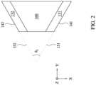
- FIG. 2is a top view of the optical structure in accordance with some embodiments.
- FIG. 3is a side view of the optical structure in accordance with some embodiments.
- FIG. 4is a top view of the optical structure in accordance with some embodiments.
- FIG. 5is a top view of the optical structure in accordance with some embodiments.
- FIG. 6is a side view from the back of the optical structure of FIG. 5 .
- FIG. 7is a side view of the optical film in accordance with some embodiments.
- FIG. 1is a perspective diagram of an optical film in accordance with some embodiments.
- an optical film 100includes a main body 110 and multiple optical structures (e.g. optical structures 120 ).
- the main body 110has a top surface 111 having a normal vector 112 .
- the optical structures 120protrude from the top surface 111 of the main body 110 .
- the optical structures 120may protrude from a bottom surface of the main body 110 .
- the optical structures 120may be formed by injection, rolling, or any method.
- the material of the optical structures 120is identical to that of the main body 110 .
- the optical structures 120are arranged along an X direction in FIG.
- the optical structure 120may also be arranged along a Y direction, and that is, the optical structures 120 may be arranged as a matrix across the optical film 100 .
- a userviews the optical film 100 from a Z direction. In other words, the user is at the upper side of FIG. 1 .
- the optical film 100allows the user to have a clear viewing angle in the X direction and ⁇ X direction, and also a clear viewing angle in the ⁇ Y direction.
- An optical structure 130is taken as an example for detailed description.
- FIG. 2is a top view of the optical structure 130 in accordance with some embodiments.
- FIG. 3is a side view from the back of the optical structure 130 in accordance with some embodiments.
- the optical structure 130has a first side surface 131 , a second side surface 132 , and a top surface 160 .
- the top surface 160is connected to the first side surface 131 and the second side surface 132 .
- a shape of the top surface 160is a trapezoid.
- the top surface 160 of the optical structure 130is parallel with the top surface 111 of the main body 110 .
- the first side surface 131is connected to the top surface 111 of the main body 110 .
- a first connecting line 141 and a first angle ⁇ 1are formed between the first side surface 131 and the top surface 111 .
- the first angle ⁇ 1is less than 90 degrees.
- the second side surface 132is also connected to the top surface 111 of the main body 110 .
- a second connecting line 142 and a second angle ⁇ 2are formed between the second side surface 132 and the top surface 111 .
- the second angle ⁇ 2is less than 90 degrees.
- the lightenters the main body 110 from below.
- the output lightis represented as vectors, then some vectors would have non-zero components in the X direction and some other vectors would have non-zero components in the ⁇ X direction due to the first angle ⁇ 1 and the second angle ⁇ 2 . Therefore, the user can see clear images from the X direction and ⁇ X direction.
- a third angle ⁇ 3is formed between an extension line 151 of the first connecting line 141 and an extension line 152 of the second connecting line 142 .
- the third angle ⁇ 3is greater than 0 degree and less than 90 degrees. In some embodiments, the third angle ⁇ 3 is greater than 10 degrees and less than 120 degrees.
- the output lightwould have non-zero component at the ⁇ Y direction due to the third angle ⁇ 3 .
- a cross product ⁇ right arrow over (V 1 ) ⁇ right arrow over (V 2 ) ⁇ of these two vectorswould have non-zero component in the Z direction.
- the first side surface 131is not connected to the second side surface 132 in the embodiment, but the first side surface 131 may be connected to the second side surface 132 in other embodiments.
- the shape of the top surface 160 of the optical structureis a triangle.
- the top surface 160 of the optical structuremay be a rhombus, a hexagon or any other shape.
- FIG. 5is a top view of the optical structure in accordance with some embodiments.
- FIG. 6is a side view from the back of the optical structure of FIG. 5 .
- the optical structurefurther includes a third side surface 133 and a fourth side surface 134 .
- the top surface 160is connected to the third side surface 133 and the fourth side surface 134 .
- a shape of each of the first side surface 131 , the second side surface 132 , the third side surface 133 , and the fourth side surface 134is a parallelogram.
- a third connecting line 143 and a fourth angle ⁇ 4are formed between the third side surface 133 and the top surface 111 of the main body 110 .
- the fourth angle ⁇ 4is less than 90 degrees.
- a fourth connecting line 144 and a fifth angle ⁇ 5are formed between the fourth side surface 134 and the top surface 111 of the main body 110 .
- the fifth angle ⁇ 5is less than 90 degrees.
- a sixth angle ⁇ 6is formed between an extension line 153 of the third connecting line 143 and an extension line 154 of the fourth connecting line 144 .
- the sixth angle ⁇ 6is greater than 0 and less than 90 degrees. In some embodiments, the sixth angle ⁇ 6 is greater than 30 degrees and less than 60 degrees.
- the output lightwould have non-zero component in the Y direction due to the sixth angle ⁇ 6 .
- the third angle ⁇ 3is formed at the left-hand side of the optical structure in the ⁇ Y direction
- the sixth angle ⁇ 6is formed at the right-hand side of the optical structure in the Y direction. Therefore, the user can see clear images from both of the Y direction and the ⁇ Y direction.
- FIG. 7is a side view of the optical film in accordance with some embodiments.
- the optical film 100further includes a planarization layer 710 over the main body 110 .
- the planarization layer 710fills the gaps between the optical structures 120 and levels with the top surfaces of the optical structures 120 .
- the refractive index of the planarization layer 710is different from that of the optical structures 120 .
Landscapes
- Physics & Mathematics (AREA)
- General Physics & Mathematics (AREA)
- Optics & Photonics (AREA)
- Engineering & Computer Science (AREA)
- Theoretical Computer Science (AREA)
- Optical Elements Other Than Lenses (AREA)
- Optical Head (AREA)
- Glass Compositions (AREA)
Abstract
Description
Claims (2)
Priority Applications (4)
| Application Number | Priority Date | Filing Date | Title |
|---|---|---|---|
| US17/319,017US12339441B2 (en) | 2021-05-12 | 2021-05-12 | Optical film |
| CN202110783943.6ACN115421224B (en) | 2021-05-12 | 2021-07-12 | Optical Film |
| CN202411254574.1ACN118962866A (en) | 2021-05-12 | 2021-07-12 | Optical Film |
| TW110126146ATWI781688B (en) | 2021-05-12 | 2021-07-15 | Optical film |
Applications Claiming Priority (1)
| Application Number | Priority Date | Filing Date | Title |
|---|---|---|---|
| US17/319,017US12339441B2 (en) | 2021-05-12 | 2021-05-12 | Optical film |
Publications (2)
| Publication Number | Publication Date |
|---|---|
| US20220365341A1 US20220365341A1 (en) | 2022-11-17 |
| US12339441B2true US12339441B2 (en) | 2025-06-24 |
Family
ID=83999607
Family Applications (1)
| Application Number | Title | Priority Date | Filing Date |
|---|---|---|---|
| US17/319,017Active2042-05-12US12339441B2 (en) | 2021-05-12 | 2021-05-12 | Optical film |
Country Status (3)
| Country | Link |
|---|---|
| US (1) | US12339441B2 (en) |
| CN (2) | CN115421224B (en) |
| TW (1) | TWI781688B (en) |
Citations (19)
| Publication number | Priority date | Publication date | Assignee | Title |
|---|---|---|---|---|
| JPH1068803A (en) | 1996-04-29 | 1998-03-10 | Lockheed Martin Corp | Film with reduced scattering |
| TW200422646A (en) | 2001-07-19 | 2004-11-01 | Global Lighting Technologies | Light redirecting films and film systems |
| US20070159696A1 (en)* | 2003-12-17 | 2007-07-12 | Kaneka Corporation | Retroreflection sheeting and film for use in retroreflection sheeting |
| US20080117515A1 (en) | 2006-11-20 | 2008-05-22 | Hon Hai Precision Industry Co., Ltd. | Two-layered optical plate and method for making the same |
| US20080129184A1 (en)* | 2006-12-05 | 2008-06-05 | Semiconductor Energy Laboratory Co., Ltd. | Plasma display panel and field emission display |
| CN101359066A (en) | 2008-09-12 | 2009-02-04 | 上海广电光电子有限公司 | Microstructure multifunction optical film diaphragm |
| US20090061150A1 (en) | 2007-08-28 | 2009-03-05 | Nissan Motor Co., Ltd. | Antireflective structure and antireflective molded body |
| JP2010145976A (en) | 2008-12-22 | 2010-07-01 | Toyobo Co Ltd | Optical filter for display screen |
| JP2010217533A (en) | 2009-03-17 | 2010-09-30 | Hitachi Maxell Ltd | Optical sheet, backlight device using the same and liquid crystal display device |
| JP2011090104A (en) | 2009-10-21 | 2011-05-06 | Dainippon Printing Co Ltd | Optical sheet, surface light source device, and transmission type display device |
| CN102216814A (en) | 2008-11-21 | 2011-10-12 | 3M创新有限公司 | Curved sided cone structures for controlling gain and viewing angle in optical film |
| CN202649646U (en) | 2012-07-09 | 2013-01-02 | 京东方科技集团股份有限公司 | Blue phase liquid-crystal display |
| CN105093363A (en) | 2014-05-22 | 2015-11-25 | 美中全照光电股份有限公司 | Optical film |
| CN106199790A (en) | 2016-01-12 | 2016-12-07 | 宁波激智科技股份有限公司 | A kind of complex optics brightness enhancement film |
| TW201819190A (en) | 2016-11-16 | 2018-06-01 | 南韓商三星Sdi股份有限公司 | Optical film for improving contrast ratio, polarizing plate including the same, and liquid crystal display including the same |
| CN109358447A (en) | 2018-01-08 | 2019-02-19 | 友达光电股份有限公司 | Optical film and display device having the same |
| TW201945811A (en) | 2018-02-28 | 2019-12-01 | 南韓商Lg化學股份有限公司 | Viewing angle compensation film, polarizing plate comprising the same, and display device comprising the same |
| US20200011505A1 (en)* | 2017-03-31 | 2020-01-09 | Toray Industries, Inc. | Reflector having tray shapes |
| TWM604898U (en) | 2020-06-11 | 2020-12-01 | 大陸商揚昕科技(蘇州)有限公司 | Backlight module and display apparatus |
- 2021
- 2021-05-12USUS17/319,017patent/US12339441B2/enactiveActive
- 2021-07-12CNCN202110783943.6Apatent/CN115421224B/enactiveActive
- 2021-07-12CNCN202411254574.1Apatent/CN118962866A/enactivePending
- 2021-07-15TWTW110126146Apatent/TWI781688B/enactive
Patent Citations (20)
| Publication number | Priority date | Publication date | Assignee | Title |
|---|---|---|---|---|
| JPH1068803A (en) | 1996-04-29 | 1998-03-10 | Lockheed Martin Corp | Film with reduced scattering |
| TW200422646A (en) | 2001-07-19 | 2004-11-01 | Global Lighting Technologies | Light redirecting films and film systems |
| US20070159696A1 (en)* | 2003-12-17 | 2007-07-12 | Kaneka Corporation | Retroreflection sheeting and film for use in retroreflection sheeting |
| US20080117515A1 (en) | 2006-11-20 | 2008-05-22 | Hon Hai Precision Industry Co., Ltd. | Two-layered optical plate and method for making the same |
| US20080129184A1 (en)* | 2006-12-05 | 2008-06-05 | Semiconductor Energy Laboratory Co., Ltd. | Plasma display panel and field emission display |
| US7940462B2 (en)* | 2007-08-28 | 2011-05-10 | Nissan Motor Co., Ltd. | Antireflective structure and antireflective molded body |
| US20090061150A1 (en) | 2007-08-28 | 2009-03-05 | Nissan Motor Co., Ltd. | Antireflective structure and antireflective molded body |
| CN101359066A (en) | 2008-09-12 | 2009-02-04 | 上海广电光电子有限公司 | Microstructure multifunction optical film diaphragm |
| CN102216814A (en) | 2008-11-21 | 2011-10-12 | 3M创新有限公司 | Curved sided cone structures for controlling gain and viewing angle in optical film |
| JP2010145976A (en) | 2008-12-22 | 2010-07-01 | Toyobo Co Ltd | Optical filter for display screen |
| JP2010217533A (en) | 2009-03-17 | 2010-09-30 | Hitachi Maxell Ltd | Optical sheet, backlight device using the same and liquid crystal display device |
| JP2011090104A (en) | 2009-10-21 | 2011-05-06 | Dainippon Printing Co Ltd | Optical sheet, surface light source device, and transmission type display device |
| CN202649646U (en) | 2012-07-09 | 2013-01-02 | 京东方科技集团股份有限公司 | Blue phase liquid-crystal display |
| CN105093363A (en) | 2014-05-22 | 2015-11-25 | 美中全照光电股份有限公司 | Optical film |
| CN106199790A (en) | 2016-01-12 | 2016-12-07 | 宁波激智科技股份有限公司 | A kind of complex optics brightness enhancement film |
| TW201819190A (en) | 2016-11-16 | 2018-06-01 | 南韓商三星Sdi股份有限公司 | Optical film for improving contrast ratio, polarizing plate including the same, and liquid crystal display including the same |
| US20200011505A1 (en)* | 2017-03-31 | 2020-01-09 | Toray Industries, Inc. | Reflector having tray shapes |
| CN109358447A (en) | 2018-01-08 | 2019-02-19 | 友达光电股份有限公司 | Optical film and display device having the same |
| TW201945811A (en) | 2018-02-28 | 2019-12-01 | 南韓商Lg化學股份有限公司 | Viewing angle compensation film, polarizing plate comprising the same, and display device comprising the same |
| TWM604898U (en) | 2020-06-11 | 2020-12-01 | 大陸商揚昕科技(蘇州)有限公司 | Backlight module and display apparatus |
Also Published As
| Publication number | Publication date |
|---|---|
| TWI781688B (en) | 2022-10-21 |
| TW202244575A (en) | 2022-11-16 |
| CN118962866A (en) | 2024-11-15 |
| CN115421224A (en) | 2022-12-02 |
| US20220365341A1 (en) | 2022-11-17 |
| CN115421224B (en) | 2024-10-01 |
Similar Documents
| Publication | Publication Date | Title |
|---|---|---|
| CN108363250B (en) | Display panel, display assembly, display device and peep-proof method thereof | |
| US9551877B2 (en) | Grating and display device | |
| KR101653099B1 (en) | Display panel | |
| US9874782B2 (en) | Curved liquid crystal display device | |
| US20190212607A1 (en) | Optical film and display device having the same | |
| CN101697045A (en) | Liquid crystal display device | |
| US20100245220A1 (en) | System for displaying images | |
| US9557596B2 (en) | Liquid crystal display | |
| CN108803151B (en) | Liquid crystal display panel and display device | |
| US12339441B2 (en) | Optical film | |
| CN105842927A (en) | Display panel and display device | |
| CN106373488A (en) | Transparent display panel | |
| US7492429B2 (en) | In-plane switching liquid crystal display with bent electrodes | |
| US20140160388A1 (en) | Liquid crystal display apparatus | |
| KR20100024638A (en) | Liquid crystal displayand the manufacturing method thereof | |
| JP3375351B2 (en) | Liquid crystal display | |
| US10656434B2 (en) | Display device with two display panels | |
| US20050243251A1 (en) | Transflective liquid crystal display with bent electrodes | |
| US20210364872A1 (en) | Optical structure, display device and method for manufacturing optical structure | |
| KR20200138558A (en) | Display device | |
| CN103869488B (en) | three-dimensional display | |
| US10739625B2 (en) | Display device | |
| US20050105015A1 (en) | Continuous domain vertical alignment liquid crystal display | |
| JP3666666B2 (en) | Retardation selection method for liquid crystal display device and retardation selection device | |
| CN111142292A (en) | display device |
Legal Events
| Date | Code | Title | Description |
|---|---|---|---|
| FEPP | Fee payment procedure | Free format text:ENTITY STATUS SET TO UNDISCOUNTED (ORIGINAL EVENT CODE: BIG.); ENTITY STATUS OF PATENT OWNER: LARGE ENTITY | |
| FEPP | Fee payment procedure | Free format text:ENTITY STATUS SET TO SMALL (ORIGINAL EVENT CODE: SMAL); ENTITY STATUS OF PATENT OWNER: LARGE ENTITY | |
| FEPP | Fee payment procedure | Free format text:ENTITY STATUS SET TO UNDISCOUNTED (ORIGINAL EVENT CODE: BIG.); ENTITY STATUS OF PATENT OWNER: LARGE ENTITY | |
| STPP | Information on status: patent application and granting procedure in general | Free format text:DOCKETED NEW CASE - READY FOR EXAMINATION | |
| FEPP | Fee payment procedure | Free format text:PETITION RELATED TO MAINTENANCE FEES GRANTED (ORIGINAL EVENT CODE: PTGR); ENTITY STATUS OF PATENT OWNER: LARGE ENTITY | |
| STPP | Information on status: patent application and granting procedure in general | Free format text:NON FINAL ACTION MAILED | |
| STPP | Information on status: patent application and granting procedure in general | Free format text:RESPONSE TO NON-FINAL OFFICE ACTION ENTERED AND FORWARDED TO EXAMINER | |
| STPP | Information on status: patent application and granting procedure in general | Free format text:FINAL REJECTION MAILED | |
| STPP | Information on status: patent application and granting procedure in general | Free format text:DOCKETED NEW CASE - READY FOR EXAMINATION | |
| STPP | Information on status: patent application and granting procedure in general | Free format text:NON FINAL ACTION MAILED | |
| STPP | Information on status: patent application and granting procedure in general | Free format text:RESPONSE TO NON-FINAL OFFICE ACTION ENTERED AND FORWARDED TO EXAMINER | |
| STPP | Information on status: patent application and granting procedure in general | Free format text:FINAL REJECTION MAILED | |
| STCF | Information on status: patent grant | Free format text:PATENTED CASE |