US12336263B2 - Metal contacts to group IV semiconductors by inserting interfacial atomic monolayers - Google Patents
Metal contacts to group IV semiconductors by inserting interfacial atomic monolayersDownload PDFInfo
- Publication number
- US12336263B2 US12336263B2US18/474,948US202318474948AUS12336263B2US 12336263 B2US12336263 B2US 12336263B2US 202318474948 AUS202318474948 AUS 202318474948AUS 12336263 B2US12336263 B2US 12336263B2
- Authority
- US
- United States
- Prior art keywords
- atoms
- semiconductor region
- semiconductor
- group
- channel transistor
- Prior art date
- Legal status (The legal status is an assumption and is not a legal conclusion. Google has not performed a legal analysis and makes no representation as to the accuracy of the status listed.)
- Active
Links
Images


Classifications
- H—ELECTRICITY
- H01—ELECTRIC ELEMENTS
- H01L—SEMICONDUCTOR DEVICES NOT COVERED BY CLASS H10
- H01L21/00—Processes or apparatus adapted for the manufacture or treatment of semiconductor or solid state devices or of parts thereof
- H01L21/02—Manufacture or treatment of semiconductor devices or of parts thereof
- H01L21/04—Manufacture or treatment of semiconductor devices or of parts thereof the devices having potential barriers, e.g. a PN junction, depletion layer or carrier concentration layer
- H01L21/18—Manufacture or treatment of semiconductor devices or of parts thereof the devices having potential barriers, e.g. a PN junction, depletion layer or carrier concentration layer the devices having semiconductor bodies comprising elements of Group IV of the Periodic Table or AIIIBV compounds with or without impurities, e.g. doping materials
- H01L21/28—Manufacture of electrodes on semiconductor bodies using processes or apparatus not provided for in groups H01L21/20 - H01L21/268
- H01L21/283—Deposition of conductive or insulating materials for electrodes conducting electric current
- H01L21/285—Deposition of conductive or insulating materials for electrodes conducting electric current from a gas or vapour, e.g. condensation
- H01L21/28506—Deposition of conductive or insulating materials for electrodes conducting electric current from a gas or vapour, e.g. condensation of conductive layers
- H01L21/28512—Deposition of conductive or insulating materials for electrodes conducting electric current from a gas or vapour, e.g. condensation of conductive layers on semiconductor bodies comprising elements of Group IV of the Periodic Table
- H01L21/28518—Deposition of conductive or insulating materials for electrodes conducting electric current from a gas or vapour, e.g. condensation of conductive layers on semiconductor bodies comprising elements of Group IV of the Periodic Table the conductive layers comprising silicides
- H—ELECTRICITY
- H01—ELECTRIC ELEMENTS
- H01L—SEMICONDUCTOR DEVICES NOT COVERED BY CLASS H10
- H01L21/00—Processes or apparatus adapted for the manufacture or treatment of semiconductor or solid state devices or of parts thereof
- H01L21/02—Manufacture or treatment of semiconductor devices or of parts thereof
- H01L21/04—Manufacture or treatment of semiconductor devices or of parts thereof the devices having potential barriers, e.g. a PN junction, depletion layer or carrier concentration layer
- H01L21/18—Manufacture or treatment of semiconductor devices or of parts thereof the devices having potential barriers, e.g. a PN junction, depletion layer or carrier concentration layer the devices having semiconductor bodies comprising elements of Group IV of the Periodic Table or AIIIBV compounds with or without impurities, e.g. doping materials
- H01L21/30—Treatment of semiconductor bodies using processes or apparatus not provided for in groups H01L21/20 - H01L21/26
- H01L21/324—Thermal treatment for modifying the properties of semiconductor bodies, e.g. annealing, sintering
- H—ELECTRICITY
- H10—SEMICONDUCTOR DEVICES; ELECTRIC SOLID-STATE DEVICES NOT OTHERWISE PROVIDED FOR
- H10D—INORGANIC ELECTRIC SEMICONDUCTOR DEVICES
- H10D62/00—Semiconductor bodies, or regions thereof, of devices having potential barriers
- H10D62/40—Crystalline structures
- H10D62/405—Orientations of crystalline planes
- H—ELECTRICITY
- H10—SEMICONDUCTOR DEVICES; ELECTRIC SOLID-STATE DEVICES NOT OTHERWISE PROVIDED FOR
- H10D—INORGANIC ELECTRIC SEMICONDUCTOR DEVICES
- H10D62/00—Semiconductor bodies, or regions thereof, of devices having potential barriers
- H10D62/80—Semiconductor bodies, or regions thereof, of devices having potential barriers characterised by the materials
- H10D62/83—Semiconductor bodies, or regions thereof, of devices having potential barriers characterised by the materials being Group IV materials, e.g. B-doped Si or undoped Ge
- H10D62/832—Semiconductor bodies, or regions thereof, of devices having potential barriers characterised by the materials being Group IV materials, e.g. B-doped Si or undoped Ge being Group IV materials comprising two or more elements, e.g. SiGe
- H—ELECTRICITY
- H10—SEMICONDUCTOR DEVICES; ELECTRIC SOLID-STATE DEVICES NOT OTHERWISE PROVIDED FOR
- H10D—INORGANIC ELECTRIC SEMICONDUCTOR DEVICES
- H10D64/00—Electrodes of devices having potential barriers
- H10D64/60—Electrodes characterised by their materials
- H10D64/62—Electrodes ohmically coupled to a semiconductor
- H—ELECTRICITY
- H10—SEMICONDUCTOR DEVICES; ELECTRIC SOLID-STATE DEVICES NOT OTHERWISE PROVIDED FOR
- H10D—INORGANIC ELECTRIC SEMICONDUCTOR DEVICES
- H10D64/00—Electrodes of devices having potential barriers
- H10D64/60—Electrodes characterised by their materials
- H10D64/64—Electrodes comprising a Schottky barrier to a semiconductor
Definitions
- the present inventionrelates to techniques for reducing the specific contact resistance of metal-semiconductor (e.g., group IV semiconductor) junctions by interposing a monolayer of group V or group III atoms at the interface between the metal and the semiconductor, or interposing a bi-layer made of one monolayer of each of group V and group III atoms, or interposing multiple such bi-layers.
- metal-semiconductore.g., group IV semiconductor
- transistorsAs the size of transistors is reduced to nanometer scale dimensions, for example in the form of ultra-thin body (UTB) silicon-on-insulator (SOI) field effect transistors (FETs), FinFETs and nanowire FETs, the unwanted resistance associated with transistor sources and drains becomes an ever increasing burden on the performance of these devices and of the integrated circuit products manufactured using such transistors. Furthermore, a reduction of dopant activation is predicted theoretically and demonstrated experimentally when the transistor source and drain regions are reduced in size below approximately 10 nm. By dopant activation, we mean desired free carrier (electron or hole) contributions from deliberately introduced impurity species in a semiconductor host.
- dopant activationwe mean desired free carrier (electron or hole) contributions from deliberately introduced impurity species in a semiconductor host.
- This decrease in nanoscale dopant activationfurther contributes to undesirably high resistance of doped source/drain (S/D) regions both at the nanoscale metal contacts and within the bulk portion of the nanoscale doped regions.
- S/Dsource/drain
- the silicon microelectronics industryhas relied on high doping concentrations in the silicon proximate metal-silicon contacts as a means of obtaining acceptably low contact resistances to transistor sources and drains.
- the contact metalhas for the most part been a metal silicide, most recently nickel silicide or nickel platinum silicide. This approach to minimizing contact resistance is expected to be insufficient in the future as the transistor dimensions continue to shrink and the contact resistance becomes a larger portion of the total resistance between the source and drain (hence becoming a serious performance-limiting factor).
- a technology that is capable of reducing the Schottky barrier and hence reducing the resistance of contacts to doped semiconductor regionsmay also be applied to so-called “metal source/drain transistors” which do not have doped source and drain but rather utilize a direct contact between the metal and the transistor channel (the region of free carriers that are modulated by the electrical potential on a gate and that transport current between the source and the drain).
- Valence band offsetswere measured by in situ core level x-ray photoluminescence.
- the deposited Ge region (overlayer)had a valence band offset to the Ge substrate as manifested by a splitting of the Ge 3d core level into two components; one due to the Ge substrate and the other to the Ge overlayer.
- Both positive and negative valence band offsetswere obtained in Ge homojunctions by introducing Ga—As dipole intralayers with either “Ga-first” or “As-first” growth sequences.
- the band offsetwas found to be 0.35-0.45 eV with the Ge valence band edge on the As side of the junction at a lower energy (i.e., more bound).
- Dipole intralayerswere explained on the basis of the Harrison “theoretical alchemy” model described by W. A. Harrison et al. in “ Polar Heterojunction Interfaces ”, Phys. Rev. B 18, 4402 (1978). Intralayer control of band discontinuities was thus applied to homojunctions, expanding the potential domain of band offset engineering beyond semiconductor heterojunctions.
- Valence band discontinuitieswere again measured by in situ core level x-ray photoluminescence.
- a deposited Ge regionoverlayer
- a deposited Si regionhad a valence band offset to a Si substrate as evidenced by a splitting of the Si 2p core level.
- group V or group III atomsor group II or group VI atoms
- group V or group III atomsare organized in single ordered (e.g., epitaxially oriented) interfacial monolayers.
- present inventionprovides a process and structure wherein a metal contact is deposited and not necessarily formed by silicidation, a feature that allows a much broader range of metals to be used for formation of metal-semiconductor contacts, particularly metals that have favorable properties over metal silicides for specific applications such as higher electrical conductance or optical transparency or ferromagnetism.
- spin-MOSFETspin-metal-oxide-semiconductor field effect transistor
- metal contactIn emissive displays it is often desirable to have a metal contact that allows good transmission of emitted light (high transparency) yet at the same time forms a low resistance contact to the active material. Conversely in photonic devices such as semiconductor lasers or modulators, it may be desirable to have metal contacts that are not transparent so as to minimize losses due to light absorption. Metal silicides have the undesirable property of being somewhat transparent, with the consequence that optical energy may enter a silicide region located within the optical field of a photonic element and subsequently be absorbed in the silicide.
- the present inventiondoes not require doping of the semiconductor proximate to the metal contact, although it may be practiced in conjunction with semiconductor doping. Nor does the present invention require a metal silicidation step.
- Devices configured in accordance with embodiments of the present inventioninclude at least an ordered monolayer of a group V and/or an ordered monolayer of a group III element or elements at the interface between a semiconductor and a metal contact. The metal is deposited after the formation of at least an ordered monolayer of interfacial atoms.
- Embodiments of the present inventionprovide electrical contacts having one or more monolayers disposed between a group IV semiconductor and a metal, the semiconductor characterized by a crystal lattice structure and a monolayer consisting of a single atomic layer of atoms of one or more group V materials or a single atomic layer of atoms of one or more group III materials, each single atomic layer being in epitaxial alignment with one another and with the semiconductor lattice; and methods of forming such electrical contacts.
- an electrical contactthat includes a metal and a group IV semiconductor separated by a monolayer of group V atoms and, optionally, a monolayer of group III atoms at an interface between the metal and the semiconductor.
- the metalmay be made of atoms of the same metallic element as the monolayer of group III metal atoms or of atoms of a different metallic element than the monolayer of group III metal atoms.
- the group III atomsmay be any one or more of aluminum, gallium, indium or boron, or mixtures of aluminum, gallium, boron and/or indium.
- the group IV semiconductormay be germanium, silicon, an alloy of germanium and silicon or germanium and tin, or an alloy or compound of silicon and/or germanium with carbon.
- the group V atomsmay be any one or more of nitrogen, phosphorus, arsenic or antimony. In some instances, one monolayer of group III atoms will be immediately adjacent the surface of the group IV semiconductor. In other cases, one monolayer of group V atoms will be immediately adjacent the surface of the group IV semiconductor.
- the surface of the group IV semiconductormay be a ⁇ 111 ⁇ -oriented surface or a ⁇ 100 ⁇ -oriented surface.
- the present inventionalso includes methods of forming electrical contacts such as those described above. In some instances, this involves a ⁇ 100 ⁇ -oriented surface of the group IV semiconductor being etched with a crystallographically selective etch to reveal and expose one or more ⁇ 111 ⁇ -oriented semiconductor crystal facets; the monolayer of group V atoms being formed on the ⁇ 111 ⁇ facets; and the monolayer of group III atoms being subsequently deposited on the monolayer of group V atoms.
- the monolayers of group V atoms and/or group III atomsmay be produced by way of separate vapor deposition processes or by separate chemical reactions.
- the ⁇ 111 ⁇ -oriented facets of the semiconductormay be cleaned in situ and the semiconductor heated to a sufficiently high temperature to obtain a 7 ⁇ 7 reconstruction in the case of a ⁇ 111 ⁇ silicon surface or a 5 ⁇ 5 reconstruction in the case of a ⁇ 111 ⁇ silicon germanium surface or a 2 ⁇ 8 reconstruction of a ⁇ 111 ⁇ germanium surface after which the semiconductor may be heated to an elevated temperature during deposition of the group V atoms and/or group III atoms.
- UHVultra-high vacuum
- metal atomsmay be deposited on the first bi-layer (two monolayers) directly or further monolayers of group V atoms and/or group III atoms may be added to create a stack of monolayers in excess of a single bi-layer before metal atoms are deposited to form a contact.
- FIGS. 1 ( a ) and 1 ( b )illustrate potential barriers at metal-semiconductor junctions; specifically FIG. 1 ( a ) shows a semiconductor (to the left)-metal (to the right) interface with a fixed and thick barrier to electron flow; and FIG. 1 ( b ) illustrates how a dipole layer interposed between the metal and semiconductor has eliminated the barrier except between one pair of atomic planes.
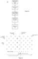
- FIG. 2illustrates an example of a process for forming a very low resistance metal contact to a semiconductor surface in accordance with an embodiment of the present invention.
- FIGS. 3 ( a ), 3 ( b ) and 3 ( c )provide views of a 7 ⁇ 7 reconstructed ⁇ 111 ⁇ -oriented silicon surface.
- FIG. 4illustrates an example of group V atoms bonded directly with exposed silicon surface atoms to form a fully coordinated lattice termination with no dangling bonds.
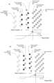
- FIG. 5illustrates a bi-layer (two monolayers) interposed on a (111) surface of an n-type semiconductor, producing a contact by the process illustrated in FIG. 2 in accordance with embodiments of the present invention.
- FIGS. 6 ( a ) and 6 ( b )illustrate double bi-layers on (111) interfaces for n-type semiconductors with fields across long or short interplanar separations, respectively.
- FIG. 7illustrates double bi-layers, as in FIG. 6 , but for p-type semiconductors, providing an extremely low resistance to the electrical conduction of holes through the contact, in accordance with further embodiments of the present invention.
- FIG. 8illustrates a process for creating the contact shown in FIG. 7 in accordance with embodiments of the present invention.
- FIG. 9illustrates one bi-layer (two monolayers), as in FIG. 5 , but for a ⁇ 100 ⁇ semiconductor surface, rather than a ⁇ 111 ⁇ surface.
- FIGS. 10 and 11illustrate experimental Schottky diode current voltage characteristics obtained from aluminum- ⁇ 111 ⁇ oriented p-type silicon contacts and compares measured data from contacts with an arsenic atomic monolayer at the interface with data from contacts with no arsenic interfacial layer.
- the present inventorshave recognized a need for a metal contact technology that can reduce the resistance of metal contacts to doped S/D regions or, alternatively, a metal-semiconductor technology that eliminates, as much as possible, the Schottky barrier between the metal and the semiconductor.
- a low resistance metal-semiconductor contacting technologywill have application wherever low resistance is required, for example in solar cell applications and in metal S/D field effect transistors (FETs).
- the present inventionrelates to techniques for reducing the specific contact resistance of metal-semiconductor (group IV) junctions by interposing a monolayer of group V or group III atoms at the interface between the metal and the semiconductor, or interposing a bi-layer made of one monolayer of group V atoms and one monolayer of group III atoms, or interposing multiple such bi-layers.
- the inventionincludes methods for forming such a metal-semiconductor contact of very low barrier height (approaching zero) and extremely low specific contact resistance by providing at least a single ordered layer of atoms at the interface between a metal and a semiconductor.
- the resulting low specific resistance metal-group IV semiconductor junctionfinds application as a low resistance electrode in semiconductor devices including electronic devices (e.g., transistors, diodes, etc.) and optoelectronic devices (e.g., lasers, solar cells, photodetectors, etc.) and/or as a metal source and/or drain region (or a portion thereof) in a FET.
- semiconductor devicesincluding electronic devices (e.g., transistors, diodes, etc.) and optoelectronic devices (e.g., lasers, solar cells, photodetectors, etc.) and/or as a metal source and/or drain region (or a portion thereof) in a FET.
- the monolayer of group V or group III atoms adjacent to the semiconductor surfaceis predominantly an ordered layer of atoms formed on the surface of the group IV semiconductor and chemically bonded to the surface atoms of the group IV semiconductor.
- the present invention's emphasis on ordered monolayers, as well as the inclusion of group V elements, such as phosphorus or antimony, and group III elements, such as aluminum, boron, gallium or indium, distinguishes it from the earlier work of Grupp and Connelly (cited above). Further, the above-cited works of Marsi et al. and McKinley et al. specified an intention to create an energy band offset between two regions of semiconductor and no mention was made of modifying a Schottky barrier between a metal and a semiconductor or even of the possibility of doing so.
- group V elementssuch as phosphorus or antimony
- group III elementssuch as aluminum, boron, gallium or indium
- the resulting bi-layerprovides an electrical dipole between the semiconductor and the bulk metal.
- a similar dipoleexists when only a single layer of group V atoms is present, as an image charge is formed in the bulk metal.
- multiple bi-layersmay be used between the semiconductor and the bulk metal (e.g., 2 or 3 such bi-layers). Indeed, dipole layers can be added until the extra energy from increasing the field causes the atoms to rearrange themselves.
- references to monolayersshould be read as encompassing monolayers of a single kind of group V or group III atoms and as monolayers of group V or group III atoms of more than one element.
- the semiconductoris a group IV semiconductor, for example germanium, silicon, an alloy of silicon and germanium, or an alloy comprising two or more of the elements silicon, germanium, carbon and tin.
- FETs or other electronic devices made up of compound semiconductorsmay also benefit from use of low resistance junctions provided in accordance with the present invention.
- the metal forming the junction with the semiconductor (and the interfacial layer of ordered group V atoms)is described as a group III metal. However, this need not necessarily be the case. It is not necessary that the metal is a group III metal.
- low work function metalssuch as magnesium, lanthanum, ytterbium or gadolinium
- high work function metalssuch as nickel, platinum, iridium or ruthenium may be preferred for obtaining low hole barriers or high electron barriers between the metal and the semiconductor.
- higher work function metalssuch as platinum or ruthenium for making contacts with low electron barriers either.
- the energy barrier between the metal Fermi level and the semiconductor conduction bandcan be low despite the metal having a high work function by virtue of the large magnitude of the dipole created by the presence of the ordered group V monolayer at the semiconductor interface.
- the metalmay be a barrier metal such as tantalum nitride (TaN) or titanium nitride (TiN) or ruthenium (Ru) and for the same barrier metal to be used in making contact to both p-type and n-type semiconductor regions.
- a barrier metalsuch as tantalum nitride (TaN) or titanium nitride (TiN) or ruthenium (Ru) and for the same barrier metal to be used in making contact to both p-type and n-type semiconductor regions.
- the interfacial monolayer chemically bonded to the semiconductor surfacewill be an interfacial layer of ordered group V atoms at n-type contacts and will be an interfacial layer of ordered group III atoms at p-type contacts.
- the interfacial monolayer chemically bonded to the semiconductor surfacewill be an interfacial layer of ordered group V atoms at source/drain junctions of n-channel MOSFETs and will be an interfacial layer of ordered group III atoms at source/drain junctions of p-channel MOSFETs.
- Ferromagnetic metalssuch as gadolinium, iron, nickel or cobalt or alloys of these elements or ferromagnetic alloys of manganese may be used to obtain metal-semiconductor contacts with high spin injection efficiency.
- the interfacial monolayer chemically bonded to the semiconductor surfaceis preferably an interfacial layer of ordered group V atoms.
- the ferromagnetic metalmay be deposited directly on to the group V monolayer or a monatomic layer of group III metal atoms may be chemically bonded to the group V atoms and the ferromagnetic metal deposited on to the group III monolayer.
- metal silicidessuch as nickel silicide of composition Ni 2 Si, NiSi or NiSi 2 or platinum silicide or cobalt silicide, or even semi-metals may be used wherein the metallic material is directly adjacent to the group V or group III monolayer. It is possible and may be most convenient in manufacturing for the same metallic material to be applied to both n-type and p-type semiconductor contacts or as the metal source and/or drain of both n-channel and p-channel MOSFETs.
- the single ordered layer of atomsis a single ordered layer of group V atoms.
- the group V atomsmay be nitrogen atoms, phosphorus atoms, arsenic atoms or antimony atoms or a mixture of these group V atoms.
- the monolayer of group V atomsis a layer of arsenic atoms ordered in epitaxial (or substantially epitaxial) alignment with the germanium or silicon or group IV semiconductor alloy crystal lattice.
- Such a contact with extremely low resistance to conduction of electronsis used for making electrical contact to n-type doped semiconductor such as the n-type doped source and drain regions of an n-channel FET or for making metal source/drain regions that make direct contact to an electron channel in an n-channel FET.
- the surface of the group IV semiconductor on which the metal contact is formedwill be a ⁇ 111 ⁇ -oriented surface and, to the greatest possible extent, each of the group V atoms in the single ordered layer of atoms is chemically bonded in a three-way coordination with atoms in the ⁇ 111 ⁇ oriented surface of the semiconductor.
- the contacted surface of the group IV semiconductorwill be a ⁇ 100 ⁇ or ⁇ 110 ⁇ surface. In some instances a ⁇ 100 ⁇ surface may be preferred.
- the Fermi energy in the metalis observed to be “pinned” at a specific energy in the semiconductor energy band gap for each semiconductor causing a barrier between the metal Fermi level and the conduction band or valence band in the semiconductor.
- the semiconductorcan be made conducting (e.g., with doping), fixing the Fermi energy E F near the semiconductor band edge E c in the bulk crystal (E F , without a voltage applied, is uniform through the system), as illustrated in FIG. 1 ( a ) , E c remains well above E F at the interface. As a consequence, the region of the semiconductor near the interface has not been made a good conductor.
- thermoelectric field emissionis a combination of thermionic emission and tunneling of electrons through the energy barrier.
- the present inventionseeks to eliminate, or at least sharply reduce, this barrier by inserting an electric dipole layer between the metal and the semiconductor, shifting the relative positions of the band edge and the Fermi energy at the interface.
- the resulting energiesare illustrated in FIG. 1 ( b ) .
- the net resultis to remove almost all of the barrier region, except for that remaining in the dipole layer.
- any suitable corresponding bi-layers of group V-group III materialsmay be used for the purpose of eliminating (or at least significantly reducing) the Schottky barrier and can be chosen for convenience or other considerations, and similarly any element of the columns IB, II, VI, and VII serve as well as the ones mentioned in the preceding paragraph. More specifically, an ordered monolayer of group VI elements sulfur and/or selenium and/or tellurium may be deposited in combination with an ordered monolayer of group II elements zinc and/or cadmium to form an ordered II-VI bi-layer.
- FIG. 2one example of a process 10 for forming a very low resistance metal contact to a semiconductor surface is illustrated.
- a ⁇ 100 ⁇ -oriented surface of the group IV semiconductor (or alloy or compounds of group IV semiconductors and/or carbon), 12is etched with a crystallographically selective etch to reveal and expose one or multiple ⁇ 111 ⁇ -oriented semiconductor crystal facets 14 .
- a monolayer of group V atomsis formed 16 on the ⁇ 111 ⁇ facets, followed by deposition 18 of a suitable group III metal to form the contact.
- the monolayer of group V atomsneed not necessarily be a perfect ordered monolayer. That is, the monolayer of group V atoms may have some gaps in coverage or some excess atoms.
- the metal atoms in step 18may be metal atoms other than group III metal atoms.
- the metalmay be an alloy of pure metals, a metal silicide or a metallic compound.
- the monolayer of group V atomsmay be produced by way of a vapor deposition process or by a chemical reaction. In the case of a vapor deposition process, this may include exposing the semiconductor at an elevated temperature to a vapor flux of group V atoms or a flux of molecules of the group V element.
- the flux of group V atoms/moleculesmay be generated by thermally evaporating a source of the group V element.
- the fluxis a flux of arsenic molecules of composition As 4 and the As 4 molecular flux is created by the thermal evaporation of an elemental arsenic source in a Knudsen cell (k-cell) as is known in the practice of molecular beam epitaxy.
- the various manufacturing tools that may be used for deposition of the group V and/or group III monolayersinclude molecular beam epitaxy (MBE), gas source molecular beam epitaxy (GSMBE), metalorganic molecular beam epitaxy (MOMBE), metalorganic chemical vapor deposition (MOCVD), metalorganic vapor phase epitaxy (MOVPE), atomic layer deposition (ALD), atomic layer epitaxy (ALE) and chemical vapor deposition (CVD) tools, including plasma-enhanced CVD (PECVD) or photon or laser-induced CVD.
- MBEmolecular beam epitaxy
- GSMBEgas source molecular beam epitaxy
- MOMBEmetalorganic molecular beam epitaxy
- MOCVDmetalorganic chemical vapor deposition
- MOVPEmetalorganic vapor phase epitaxy
- ALDatomic layer deposition
- ALEatomic layer epitaxy
- CVDchemical vapor deposition
- PECVDplasma-enhanced CVD
- Another vapor deposition processthat may be used in accordance with embodiments of the present invention involves the group V element atoms being deposited on the semiconductor surface by decomposition of a vapor phase compound of the group V element, for example a hydride of the group V element.
- Suitable group V hydride gasesinclude ammonia, NH 3 , for nitrogen atom deposition; phosphine, PH 3 , for phosphorus; arsine, AsH 3 , for arsenic and stibine, SbH 3 , for the deposition of an antimony atomic layer.
- the vapor phase compound of the desired group V elementcould be a metalorganic compound, examples of such being an alkyl arsine such as tertiary butyl arsine for the deposition of an arsenic monolayer or an alkyl stibine such as triethylantimony (triethylstibine) for the deposition of an antimony monolayer.
- an alkyl arsinesuch as tertiary butyl arsine for the deposition of an arsenic monolayer
- an alkyl stibinesuch as triethylantimony (triethylstibine) for the deposition of an antimony monolayer.
- FIGS. 3 ( a )(perspective view), 3 ( b ) (plan view of primitive unit cell) and 3 ( c ) (side view of primitive unit cell) provide views of such a 7 ⁇ 7 surface 20 .
- Atoms 22represent atoms in the underlying (1 ⁇ 1) bulk silicon material.
- Atoms 24represent so-called rest atoms (atoms one layer below the adatoms).
- Atoms 26represent dimers (paired surface silicon atoms).
- Atoms 28represent the adatoms (silicon atoms laying on the crystal surface). Corner holes in the structure are shown at 30 .
- the siliconis maintained at a temperature in the range of approximately 20° C. to 750° C. (inclusive) during exposure to the group V atom vapor or the group V compound molecular vapor.
- the silicon surfacemay be exposed to the group V atom or compound molecular vapor flux for less than one second or several seconds or even several minutes.
- the silicon held at a suitable temperaturean ordered monolayer of the group V atom is formed and, after so forming, the monolayer resists the deposition of additional group V atoms or deposition of other atoms such as hydrogen or oxygen or carbon atoms.
- the semiconductor temperaturemay be varied during exposure to the group V atom vapor or the group V molecular compound vapor, starting at a high temperature in the range 600 C to 800° C. and reducing to a lower temperature in the range 500 C to 20° C.
- the group V atoms 32(e.g., As, Sb or P) bond directly with the exposed silicon surface atoms 34 to form a fully coordinated lattice termination with, to the greatest extent possible, no dangling bonds, as shown in FIG. 4 , which is a side view of the resulting structure.
- Three of the five valence electrons in each group V atomform bonds with silicon atoms at the surface of the group IV semiconductor and the remaining two valence electrons form a “lone-pair” orbital as shown in the illustration.
- Similar processesmay be applied to obtain monolayers of group V atoms on silicon surfaces other than the ⁇ 111 ⁇ orientation, such as a ⁇ 100 ⁇ orientated silicon surface. Similar processes may also be applied to obtain monolayers of group V atoms on group IV semiconductor surfaces other than silicon, such semiconductors including germanium, silicon germanium, silicon carbon, germanium tin or silicon germanium carbon. Moreover similar processes may also be applied to obtain monolayers of group VI atoms on group IV semiconductor surfaces.
- the exposure of the surface of a heated semiconductor to the group V atom flux or compound molecular fluxmay be done in an ultra-high vacuum (UHV) chamber, in a vacuum chamber or in a reduced pressure chamber. If the chamber in which the process occurs is not a UHV chamber, a background or carrier gas may be present during the exposure.
- UHVultra-high vacuum
- a background or carrier gasmay be present during the exposure.
- arsine, AsH 3is delivered in dilute form in a gas mixture consisting primarily of hydrogen (H 2 ) or nitrogen (N 2 ).
- arsineis typically diluted at a concentration of a few percent or even as low as 100 parts per million or so in ultra pure hydrogen or nitrogen.
- the arsinewhether it be pure arsine or a dilute mixture of one or a few percent arsine in hydrogen or nitrogen, decomposes at the heated semiconductor surface, liberating free arsenic atoms that bond directly with the exposed silicon surface to form a fully coordinated lattice termination with no, or at least very few, dangling bonds.
- a preferred process for the deposition of a monolayer of arsenic on silicon from a hydride precursor gas (AsH 3 )starts by heating the silicon surface in a hydrogen ambient to a temperature sufficient to reduce any surface oxide then continues by heating the silicon surface to a temperature in the range 650° C. to 750° C. (most preferably between 675° C. and 725° C.) while exposing the surface to AsH 3 vapor for a period of between 10 seconds to 30 minutes (most preferably between 20 seconds and 2 minutes).
- Such a processmay be carried out in a CVD system or an ALD system and an ordered monolayer of arsenic atoms is formed.
- the monolayerresists the deposition of additional group V atoms or deposition of other atoms such as hydrogen or oxygen or carbon atoms.
- the semiconductor temperaturemay be varied during exposure to the AsH 3 vapor, starting at a high temperature in the range 650° C. to 750° C. and reducing to a lower temperature in the range 500° C. to 20° C.
- the group V atomsform a perfect monolayer.
- a metalcould be deposited on top of this group V monolayer, or more silicon and then the metal.
- the monolayer of chargemay exist at the interfacial layer (as described above) or at the second, third or fourth planes from the semiconductor-metal interface if one, two or three atomic layers of silicon respectively are deposited after the group V monolayer and before the metal.
- one monolayer of a group III metal atoms 40is deposited in the embodiment illustrated in FIG. 5 , followed by the deposition of the metal contact (bulk metal atoms 42 ), providing the low barrier, low resistance metal contact,
- the one layer of metal atoms 40is a layer of group III metal atoms that may include aluminum, gallium or indium or a mixture of these group III metal atoms.
- metals or alloys of metals other than or in combination with a group III metalmay be used.
- This monolayer of group III metal atomsis optional and need not necessarily be present in all junctions formed in accordance with the present invention (a balancing negative charge (described further below) would be an image charge formed in the bulk metal).
- the metal atoms in the one layer of metal atomsare preferably coordinated with the monolayer of group V atoms already present on the semiconductor surface so as to form an ordered layer of metal atoms.
- the first layer of metal atomsis not strongly coordinated by chemical bonding to the underlying ordered layer of group V atoms.
- the processthen continues to deposit further metal atoms 42 , the further atoms being of the same metallic element as the first layer of metal atoms or atoms of a metal element different from the first layer of metal atoms.
- FIG. 5would illustrate the resulting structure if one makes atoms 40 and 42 the same element.
- FIG. 5a single bi-layer that includes a monolayer of group V atoms 38 and a monolayer of group III atoms 40 disposed between the semiconductor atoms 36 and bulk metal 42 is represented.
- the two plots, (a) and (b), in the illustrationrepresent the potentials at various locations across the junction, with plot (a) showing the first step in the theoretical alchemy without the polarization of neighboring bonds and plot (b) taking such relaxation into account.
- Plot (b)is somewhat exaggerated to highlight the nature of the potentials experienced across the junction.
- the monolayer of group III metal atomsmay be produced by a vapor deposition process or by a chemical reaction.
- the one layer of metal atomsmay be formed on the semiconductor surface by exposure of the surface to an atomic vapor flux of the group III metal element or to a vapor flux of a compound of the metallic element. Exposure may be for a duration of less than one second or a duration of several seconds or even several minutes.
- the vapor deposition processmay involve exposure of the semiconductor with the monolayer of Group V atoms to a vapor flux of metal atoms or a flux of molecules of the metallic element.
- the flux of metal atoms/moleculesmay be generated by thermally evaporating a source of the metal.
- the fluxis a flux of aluminum atoms created by the thermal evaporation of an elemental aluminum source in a Knudsen cell (k-cell) as is known in the practice of molecular beam epitaxy or evaporation of an elemental aluminum source by heating with an electron beam.
- the semiconductormay be heated during the deposition of the metal atoms.
- the metal atomsmay be deposited on the semiconductor surface by decomposition of a vapor phase chemical compound of the metal, for example a metalorganic compound. Such a process may be classified most generally as a chemical vapor deposition process. Suitable metalorganic compounds of aluminum include tri-methyl aluminum. Deposition of a monolayer of metal atoms from decomposition of a chemical vapor source is known more specifically as atomic layer epitaxy if the metal atoms enter into an epitaxial alignment to the semiconductor crystal lattice or atomic layer deposition if the metal atoms do not. In another alternative vapor deposition process, the metal atoms may possibly be deposited by sputtering of the metal atoms from a solid source in what is known as a physical vapor deposition (PVD) process.
- PVDphysical vapor deposition
- processingmay continue by depositing additional layers of metal atoms (which may be the same metal as the monolayer of group III atoms or a different metal).
- the further additional layers of metal atomsmay be of elemental composition and thickness in accordance with the requirements of the specific application of the resulting metal-semiconductor contact.
- the additional layers of metal atomsmay be layers of a barrier metal such as tantalum nitride, titanium nitride or ruthenium.
- a barrier metalis a thin metal layer usually deposited by a conformal deposition technique such as atomic layer deposition (ALD), plasma enhanced ALD or chemical vapor deposition (CVD) that provides a barrier to the diffusion of a copper metallization layer into the semiconductor.
- ALDatomic layer deposition
- CVDchemical vapor deposition
- the barrier metalmay be deposited in an electrochemical deposition process or by reactive physical vapor deposition (PVD) wherein the metal is sputtered from a solid source or target.
- the additional layers of metal atomsmay constitute a metal silicide such as a nickel silicide of composition Ni 2 Si, NiSi or NiSi 2 or a platinum silicide or nickel-platinum silicide or cobalt silicide wherein the metal silicide is directly adjacent to the group V monolayer or to the group V-group III bi-layer.
- a metal silicidesuch as a nickel silicide of composition Ni 2 Si, NiSi or NiSi 2 or a platinum silicide or nickel-platinum silicide or cobalt silicide wherein the metal silicide is directly adjacent to the group V monolayer or to the group V-group III bi-layer.
- a monolayer of a group V materialsuch as arsenic, phosphorus, etc.
- a group V materialsuch as arsenic, phosphorus, etc.
- the silicon surfacecan be prepared in other known ways so that group V atoms are present near the silicon surface.
- the group V materialis deposited in an appropriate manner for the monolayer to form on the silicon surface. The objective of this is that the additional group V atoms in the silicon advantageously form additional dipoles with image charges in the metal deposited on the monolayer of group V material, favorably increasing the overall dipole effect.
- FIGS. 6 ( a ) and 6 ( b )are further examples of metal-semiconductor contacts configured in accordance with embodiments of the present invention.
- contact 44is similar to the one illustrated in FIG. 5 , but includes an additional bi-layer of a group V element and a group III metal.
- the electrical dipoleis created across the long interlayer separation (i.e., the relatively long distance between the constituent monolayers 38 and 40 of the bi-layer).
- contact 44 ′has an electrical dipole across the short interlayer separation (i.e., the relatively short distance between the constituent monolayers 38 and 40 of the bi-layer).
- the single ordered layer of atomsis a single ordered layer of metal atoms 40 and includes a single atomic layer of group V atoms 38 chemically bonded to the monolayer of metal atoms and separated from the semiconductor 36 surface atoms by the monolayer of metal atoms 40 .
- the single atomic layer of metal atomsis a monolayer of group III metal atoms that may be aluminum atoms, gallium atoms or indium atoms or a mixture of these group III metal atoms.
- the monolayer of group III metal atomsis a layer of indium atoms ordered in epitaxial (or substantially epitaxial) alignment with the germanium or silicon or group IV semiconductor alloy crystal lattice and an adjacent monolayer of group V atoms is chemically bound to the monolayer of metal atoms.
- the group V atomsmay be nitrogen atoms, phosphorus atoms, arsenic atoms or antimony atoms or a mixture of these group V atoms.
- the monolayer of group V atomsis a layer of arsenic atoms ordered in alignment with and chemically bonded to the group III metal atoms that form a single atomic layer in crystallographic alignment with and chemically bonded to the surface atoms of the germanium or silicon or group IV semiconductor alloy crystal lattice.
- group III metal atomsthat form a single atomic layer in crystallographic alignment with and chemically bonded to the surface atoms of the germanium or silicon or group IV semiconductor alloy crystal lattice.
- two bi-layers between the semiconductor and the bulk metalare shown, but embodiments that include a single bi-layer are also contemplated within the scope of the present invention.
- the contacted surfaceis a ⁇ 111 ⁇ -oriented semiconductor surface. In other embodiments the contacted surface of the semiconductor is a ⁇ 100 ⁇ -oriented surface.
- FIG. 8illustrates a process 45 for creating the contact shown in FIG. 7 .
- the (100) surfaceis etched with a crystallographically selective etch to reveal and expose one or multiple ⁇ 111 ⁇ oriented semiconductor crystal facets 48 .
- a monolayer of group III metal atomsis formed on the ⁇ 111 ⁇ facets 50 , followed by deposition of a monolayer of group V atoms 52 .
- the processcontinues by depositing further multiple layers of metal 54 .
- the further additional layers of metal atomsmay be of elemental composition and thickness in accordance with the requirements of the specific application of the resulting metal-semiconductor contact, as previously described for the formation of contacts to n-type semiconductors with extremely low resistance to electron conduction.
- the monolayer of group III metal atomsmay be produced by a vapor deposition process or by a chemical reaction.
- the semiconductoris exposed to a vapor flux of group III metal atoms or a flux of molecules of a compound of the group III metal element.
- the flux of group III atoms/moleculesmay be generated by thermally evaporating a source of the group III element.
- the fluxis a flux of indium atoms created by the thermal evaporation of an elemental indium source in a Knudsen cell (k-cell) as is known in the practice of molecular beam epitaxy.
- the group III element atomsare deposited on the semiconductor surface by decomposition of a vapor phase compound of the group III element, for example a metalorganic compound of the group III element.
- a vapor phase precursor compound of the group III metalmay be achieved by heating of the semiconductor surface. Where it is preferred not to heat the semiconductor surface to very high temperatures, decomposition may be achieved by plasma in a plasma-enhanced CVD (PECVD) or plasma-enhanced ALD (PEALD) type of tool and process.
- PECVDplasma-enhanced CVD
- PEALDplasma-enhanced ALD
- decomposition of the metal precursormay be achieved by a photon-induced process.
- the semiconductor with the ⁇ 111 ⁇ -oriented surfacemay be cleaned in situ before it is exposed to the group III atom or group III molecular compound vapor flux, for example by heating it to a sufficiently high temperature under ultra-high vacuum conditions to obtain for the case of silicon a 7 ⁇ 7 reconstruction of the ⁇ 111 ⁇ silicon surface. Then the semiconductor is maintained at a temperature in the range 20° C. to 750° C. inclusive during exposure to the group III atom vapor or the group III molecular compound vapor. Alternatively the semiconductor temperature may be varied during exposure to the group III atom vapor or the group III molecular compound vapor, starting at a high temperature in the range 600 C to 800° C. and reducing to a lower temperature in the range 500 C to 20° C.
- the semiconductor surfacemay be exposed to the group III atom or compound vapor flux for less than one second or several seconds or even several minutes.
- the group III atomsbond directly with the exposed group IV semiconductor surface to form a monolayer of group III atoms, the group III atoms being to the greatest extent possible in crystallographic alignment with the semiconductor lattice.
- the exposure of the surface of the semiconductor to the group III atom flux or molecular compound vapor fluxmay be done in a UHV chamber, in a vacuum chamber or in a reduced pressure chamber. If the chamber in which the process occurs is not a UHV chamber, a background or carrier gas may be present during the exposure.
- a metalorganic compound precursorsuch as trimethyl indium is delivered in dilute form in a gas mixture consisting primarily of a carrier gas such as hydrogen or nitrogen and decomposes at the heated semiconductor surface, liberating indium atoms that bond directly with the exposed silicon.
- the metalorganic compoundis trimethyl aluminum or trimethyl gallium, which reacts at the heated semiconductor surface to form a monolayer of aluminum or gallium atoms, respectively.
- formation of the low barrier, low resistance metal contactcontinues by deposition of one layer of group V atoms.
- the group V atoms in the one layer of group V atomsare preferably coordinated with the monolayer of group III metal atoms already present on the semiconductor surface so as to form an ordered layer of group V atoms.
- the processthen continues to deposit further metal atoms, the further atoms being of the same metallic element as the first layer of metal atoms or atoms of a metal element different from the first layer of metal atoms.
- the low barrier, low resistance metal contactcontinues by deposition of a metal over the monolayer.
- the metalis not necessarily a group V metal.
- the metalmay be one having desirable properties such as structural or chemical stability to ensure reliability of the electrical contact or device so formed. Examples of stable metals for contacts include platinum (Pt), tungsten (W) and the previously described “barrier metals” TaN, TiN and Ru.
- a metalcould be deposited directly on top of the group III monolayer, such that the group III monolayer is exactly at the interface between the metal and the semiconductor or alternatively the group III monolayer may be separated from the metal by one or two monolayers of the group IV semiconductor.
- the monolayer of charge associated with the group III monolayermay exist at the interfacial layer or at the second or third planes from the semiconductor-metal interface if one or two atomic layers of group IV semiconductor respectively are intermediate between the group III monolayer and the metal.
- An advantage of having one or several atomic layers of silicon atoms between and therefore separating the monolayer of charged group III atoms (ions) and the metal atomsis the increased magnitude of the charge dipole so created between the layers and hence the greater reduction of the Schottky barrier at a metal-p-type semiconductor junction or at a metal to p-channel source/drain junction of a MOSFET.
- Another embodiment of the inventionforms a metal semiconductor contact with a monolayer of group V or group III atoms at the metal-semiconductor interface where the group V (for example arsenic) monolayer or group III (for example boron) monolayer is formed by segregation of group V or group III atoms out of a layer of material in contact with the semiconductor surface.
- the layer of materialmay be deposited on the semiconductor surface, for example by CVD or PVD.
- the group V atomsmay be introduced into the layer of material by including them as a dopant in the CVD or PVD deposition process or by ion implantation.
- the layer of materialmay be formed by reaction of another element or elements with the semiconductor surface in which case the group V or group III atoms may be implanted either before or after the material is formed by chemical reaction.
- the layermay be silicon oxide or silicon nitride formed by thermal oxidation of a silicon surface and the group V or group III atoms may be introduced into the silicon oxide or nitride layer by ion implantation.
- the layermay be a deposited thin film of doped silicon oxide containing a high concentration of a group V element such as phosphorus or a group III element such as boron.
- the formeris generally known as a “phosphosilicate glass” (“PSG”) and the latter as a “borosilicate glass” (“BSG”) and methods for deposition of these doped silicate glasses (such as CVD) are well known and widely practiced in the microelectronics industry.
- the layer of materialmay be a metal silicide formed by reaction of a metal with a silicon surface and the group V or group III atoms may be introduced into the metal silicide layer by ion implantation.
- the whole layer structureis annealed at a sufficiently high temperature to cause the group V or group III atoms to segregate to the interface form an ordered monolayer of group V or group III atoms at the interface with the group V or group III atoms bonded in epitaxial coordination with the top layer of semiconductor atoms.
- the layer of materialis a doped silicon oxide (e.g.
- the semiconductoris silicon
- the silicon oxide (or nitride)is subsequently removed by selective wet chemical etching, leaving behind a coordinated monolayer of the group V or group III atoms at the semiconductor surface, and a metal is deposited to form a metal contact to the semiconductor.
- the metal silicidemay be removed or may be retained in place to function as the metal contact itself.
- FIG. 9illustrates an example of a contact that includes such a surface, this contact including a monolayer of group V atoms that has been deposited on the group IV semiconductor ⁇ 100 ⁇ surface using any of the above-discussed techniques.
- a monolayer of group III metal atomsis then deposited on the group V atoms, followed by deposition of further metal layers.
- These further metal atomsmay be of the same metallic element as the first layer of metal atoms or atoms of a metal element different from the first layer of metal atoms.
- Experimental Schottky diodeshave been fabricated to illustrate the effect of an arsenic interfacial monolayer on an example aluminum-silicon Schottky barrier.
- the example experimentsdo not represent typical process conditions nor do they necessarily represent optimal process conditions.
- the illustrative experimentswere done on ⁇ 111 ⁇ -oriented silicon wafers, doped p-type with a boron concentration of approximately 1 ⁇ 10 17 atoms/cm 3 .
- a first set of experimental Schottky diodeswas fabricated under ultra-high vacuum conditions and a second set under low pressure chemical vapor deposition conditions in a hydrogen atmosphere.
- the first set of diodeswas processed as follows: After heating the silicon to a high temperature above 800° C. in ultra high vacuum to clean and reconstruct the ⁇ 111 ⁇ Si surface to 7 ⁇ 7, the temperature was reduced from 800° C. to 700° C. and then the silicon surface was exposed to a flux of arsenic molecules of type As 2 for ten minutes before the As 2 flux was terminated. Rutherford back scattering analysis confirmed that an areal density of arsenic equal to 7.30 ⁇ 10 14 atoms/cm 2 resulted from this exposure, a value that is close to the known areal density 7.83 ⁇ 10 14 atoms/cm 2 of surface atoms on a 1 ⁇ 1 reconstructed ⁇ 111 ⁇ silicon surface.
- FIG. 10shows representative measured current versus voltage characteristics of these experimental diodes, taking equally sized diodes from each wafer (with and without the arsenic). Diodes on wafers without arsenic at the interface consistently exhibit a relatively small Schottky barrier height to the p-type silicon as indicated by the measured curve 72 in FIG. 10 .
- a barrier heightmay be extracted by fitting a standard diode equation (thermionic emission model) to the measured data.
- the extracted barrier height for diodes without arsenic exposureis 0.40 eV (with an experimental error of approximately 0.03 eV), which is consistent with published values of barrier height for intimate aluminum contacts on p-type silicon.
- Diodes on wafers that had the silicon interface exposed to arsenic so as to form a monolayerconsistently exhibit a larger Schottky barrier height to the p-type silicon as indicated by data curve 70 in FIG. 10 .
- the larger barrier height to p-type siliconis indicative of a smaller barrier height to n-type silicon according to the general rule that the sum of magnitudes of the n-type and p-type barrier heights is very close to the silicon band gap.
- a monolayer of arsenic introduced at the interface between aluminum and a ⁇ 111 ⁇ oriented silicon surfacedoes provide a larger Schottky barrier to p-type silicon consistent with a reduced electron barrier between the aluminum Fermi level and the conduction band of the silicon (i.e. consistent with a reduced Schottky barrier height to n-type silicon).
- the second set of diodeswas processed as follows: After heating the silicon to 900° C. in a flow of hydrogen gas to clean the ⁇ 111 ⁇ Si surface, the temperature was reduced from 900° C. to 700° C. and then the silicon surface was exposed to a flux of arsine (AsH 3 ) molecules for ten minutes with the temperature held at 700° C. before the AsH 3 flow was terminated.
- the arsinewas heavily diluted in hydrogen (H 2 ) at a concentration of approximately 2 parts per million with a total gas flow of 20.4 liters per minute.
- FIG. 11shows representative measured current versus voltage characteristics of these experimental diodes (with and without the arsenic). Diodes on wafers without arsenic at the interface consistently exhibit a relatively small Schottky barrier height to the p-type silicon as indicated by the measured curve 82 in FIG. 11 . From curve 82 , a barrier height may be extracted by fitting a standard diode equation (thermionic emission model) to the measured data.
- the extracted barrier height for diodes without arsenic exposureis 0.42 eV (with an experimental error of approximately 0.03 eV), which is consistent with published values of barrier height for intimate aluminum contacts on p-type silicon.
- Diodes on wafers that had the silicon interface exposed to arsenic so as to form a monolayerconsistently exhibit a larger Schottky barrier height to the p-type silicon as indicated by data curve 80 in FIG. 11 .
- the larger barrier height to p-type siliconis indicative of a smaller barrier height to n-type silicon according to the general rule that the sum of magnitudes of the n-type and p-type barrier heights is very close to the silicon band gap.
Landscapes
- Engineering & Computer Science (AREA)
- Physics & Mathematics (AREA)
- Condensed Matter Physics & Semiconductors (AREA)
- General Physics & Mathematics (AREA)
- Manufacturing & Machinery (AREA)
- Computer Hardware Design (AREA)
- Microelectronics & Electronic Packaging (AREA)
- Power Engineering (AREA)
- Electrodes Of Semiconductors (AREA)
- Insulated Gate Type Field-Effect Transistor (AREA)
Abstract
Description
Claims (14)
Priority Applications (2)
| Application Number | Priority Date | Filing Date | Title |
|---|---|---|---|
| US18/474,948US12336263B2 (en) | 2011-11-23 | 2023-09-26 | Metal contacts to group IV semiconductors by inserting interfacial atomic monolayers |
| US19/207,282US20250275218A1 (en) | 2011-11-23 | 2025-05-13 | Metal contacts to group iv semiconductors by inserting interfacial atomic monolayers |
Applications Claiming Priority (9)
| Application Number | Priority Date | Filing Date | Title |
|---|---|---|---|
| US201161563478P | 2011-11-23 | 2011-11-23 | |
| PCT/US2012/060893WO2013077954A1 (en) | 2011-11-23 | 2012-10-18 | Improving metal contacts to group iv semiconductors by inserting interfacial atomic monolayers |
| US201414360473A | 2014-05-23 | 2014-05-23 | |
| US15/146,562US9755038B2 (en) | 2011-11-23 | 2016-05-04 | Metal contacts to group IV semiconductors by inserting interfacial atomic monolayers |
| US15/684,707US10505005B2 (en) | 2011-11-23 | 2017-08-23 | Metal contacts to group IV semiconductors by inserting interfacial atomic monolayers |
| US16/706,510US10879366B2 (en) | 2011-11-23 | 2019-12-06 | Metal contacts to group IV semiconductors by inserting interfacial atomic monolayers |
| US17/247,803US11610974B2 (en) | 2011-11-23 | 2020-12-23 | Metal contacts to group IV semiconductors by inserting interfacial atomic monolayers |
| US18/173,541US11804533B2 (en) | 2011-11-23 | 2023-02-23 | Metal contacts to group IV semiconductors by inserting interfacial atomic monolayers |
| US18/474,948US12336263B2 (en) | 2011-11-23 | 2023-09-26 | Metal contacts to group IV semiconductors by inserting interfacial atomic monolayers |
Related Parent Applications (1)
| Application Number | Title | Priority Date | Filing Date |
|---|---|---|---|
| US18/173,541ContinuationUS11804533B2 (en) | 2011-11-23 | 2023-02-23 | Metal contacts to group IV semiconductors by inserting interfacial atomic monolayers |
Related Child Applications (1)
| Application Number | Title | Priority Date | Filing Date |
|---|---|---|---|
| US19/207,282ContinuationUS20250275218A1 (en) | 2011-11-23 | 2025-05-13 | Metal contacts to group iv semiconductors by inserting interfacial atomic monolayers |
Publications (2)
| Publication Number | Publication Date |
|---|---|
| US20240030306A1 US20240030306A1 (en) | 2024-01-25 |
| US12336263B2true US12336263B2 (en) | 2025-06-17 |
Family
ID=48470199
Family Applications (9)
| Application Number | Title | Priority Date | Filing Date |
|---|---|---|---|
| US14/360,473ActiveUS9362376B2 (en) | 2011-11-23 | 2012-10-18 | Metal contacts to group IV semiconductors by inserting interfacial atomic monolayers |
| US15/043,035ActiveUS9484426B2 (en) | 2011-11-23 | 2016-02-12 | Metal contacts to group IV semiconductors by inserting interfacial atomic monolayers |
| US15/146,562ActiveUS9755038B2 (en) | 2011-11-23 | 2016-05-04 | Metal contacts to group IV semiconductors by inserting interfacial atomic monolayers |
| US15/684,707Active2032-12-23US10505005B2 (en) | 2011-11-23 | 2017-08-23 | Metal contacts to group IV semiconductors by inserting interfacial atomic monolayers |
| US16/706,510ActiveUS10879366B2 (en) | 2011-11-23 | 2019-12-06 | Metal contacts to group IV semiconductors by inserting interfacial atomic monolayers |
| US17/247,803Active2033-07-16US11610974B2 (en) | 2011-11-23 | 2020-12-23 | Metal contacts to group IV semiconductors by inserting interfacial atomic monolayers |
| US18/173,541ActiveUS11804533B2 (en) | 2011-11-23 | 2023-02-23 | Metal contacts to group IV semiconductors by inserting interfacial atomic monolayers |
| US18/474,948ActiveUS12336263B2 (en) | 2011-11-23 | 2023-09-26 | Metal contacts to group IV semiconductors by inserting interfacial atomic monolayers |
| US19/207,282PendingUS20250275218A1 (en) | 2011-11-23 | 2025-05-13 | Metal contacts to group iv semiconductors by inserting interfacial atomic monolayers |
Family Applications Before (7)
| Application Number | Title | Priority Date | Filing Date |
|---|---|---|---|
| US14/360,473ActiveUS9362376B2 (en) | 2011-11-23 | 2012-10-18 | Metal contacts to group IV semiconductors by inserting interfacial atomic monolayers |
| US15/043,035ActiveUS9484426B2 (en) | 2011-11-23 | 2016-02-12 | Metal contacts to group IV semiconductors by inserting interfacial atomic monolayers |
| US15/146,562ActiveUS9755038B2 (en) | 2011-11-23 | 2016-05-04 | Metal contacts to group IV semiconductors by inserting interfacial atomic monolayers |
| US15/684,707Active2032-12-23US10505005B2 (en) | 2011-11-23 | 2017-08-23 | Metal contacts to group IV semiconductors by inserting interfacial atomic monolayers |
| US16/706,510ActiveUS10879366B2 (en) | 2011-11-23 | 2019-12-06 | Metal contacts to group IV semiconductors by inserting interfacial atomic monolayers |
| US17/247,803Active2033-07-16US11610974B2 (en) | 2011-11-23 | 2020-12-23 | Metal contacts to group IV semiconductors by inserting interfacial atomic monolayers |
| US18/173,541ActiveUS11804533B2 (en) | 2011-11-23 | 2023-02-23 | Metal contacts to group IV semiconductors by inserting interfacial atomic monolayers |
Family Applications After (1)
| Application Number | Title | Priority Date | Filing Date |
|---|---|---|---|
| US19/207,282PendingUS20250275218A1 (en) | 2011-11-23 | 2025-05-13 | Metal contacts to group iv semiconductors by inserting interfacial atomic monolayers |
Country Status (6)
| Country | Link |
|---|---|
| US (9) | US9362376B2 (en) |
| KR (2) | KR101898027B1 (en) |
| CN (2) | CN107578994B (en) |
| DE (1) | DE112012004882B4 (en) |
| GB (3) | GB2526951B (en) |
| WO (1) | WO2013077954A1 (en) |
Families Citing this family (10)
| Publication number | Priority date | Publication date | Assignee | Title |
|---|---|---|---|---|
| US9917158B2 (en) | 2013-07-30 | 2018-03-13 | Samsung Electronics Co., Ltd. | Device contact structures including heterojunctions for low contact resistance |
| US9685509B2 (en) | 2013-07-30 | 2017-06-20 | Samsung Electronics Co., Ltd. | Finfet devices including high mobility channel materials with materials of graded composition in recessed source/drain regions |
| US20150263117A1 (en)* | 2014-03-13 | 2015-09-17 | Kabushiki Kaisha Toshiba | Semiconductor device and manufacturing method thereof |
| US9620611B1 (en) | 2016-06-17 | 2017-04-11 | Acorn Technology, Inc. | MIS contact structure with metal oxide conductor |
| US20180076324A1 (en)* | 2016-09-14 | 2018-03-15 | Applied Materials, Inc. | Method of contact formation between metal and semiconductor |
| WO2018094205A1 (en) | 2016-11-18 | 2018-05-24 | Acorn Technologies, Inc. | Nanowire transistor with source and drain induced by electrical contacts with negative schottky barrier height |
| WO2019217231A1 (en)* | 2018-05-06 | 2019-11-14 | Applied Materials, Inc. | Barrier for copper metallization and methods of forming |
| CN111370522A (en)* | 2018-12-26 | 2020-07-03 | 君泰创新(北京)科技有限公司 | Silicon heterojunction solar cell, back field structure and preparation method thereof |
| CN111370521A (en)* | 2018-12-26 | 2020-07-03 | 君泰创新(北京)科技有限公司 | Silicon heterojunction solar cell and its emitter and method for making the same |
| WO2025089830A1 (en)* | 2023-10-27 | 2025-05-01 | 주성엔지니어링(주) | Method for forming graphene electrode and method for manufacturing solar cell using same |
Citations (220)
| Publication number | Priority date | Publication date | Assignee | Title |
|---|---|---|---|---|
| GB122594A (en) | 1918-08-08 | 1919-01-30 | George Knight Letts | Improvements relating to Kettles, Saucepans, and the like. |
| US2981877A (en) | 1959-07-30 | 1961-04-25 | Fairchild Semiconductor | Semiconductor device-and-lead structure |
| US3614548A (en) | 1969-06-18 | 1971-10-19 | Matsushita Electronics Corp | Semiconductor device having a t{11 o{11 -s{11 o{11 {0 composite oxide layer |
| US3623925A (en) | 1969-01-10 | 1971-11-30 | Fairchild Camera Instr Co | Schottky-barrier diode process and devices |
| US3719797A (en) | 1971-12-16 | 1973-03-06 | Bell Telephone Labor Inc | Solid state temperature sensor employing a pair of dissimilar schottky-barrier diodes |
| US3877054A (en) | 1973-03-01 | 1975-04-08 | Bell Telephone Labor Inc | Semiconductor memory apparatus with a multilayer insulator contacting the semiconductor |
| US3983264A (en) | 1972-07-20 | 1976-09-28 | Texas Instruments Incorporated | Metal-semiconductor ohmic contacts and methods of fabrication |
| US4110488A (en) | 1976-04-09 | 1978-08-29 | Rca Corporation | Method for making schottky barrier diodes |
| US4278830A (en) | 1977-09-29 | 1981-07-14 | Nasa | Schottky barrier solar cell |
| US4304042A (en) | 1978-11-13 | 1981-12-08 | Xerox Corporation | Self-aligned MESFETs having reduced series resistance |
| EP0042066A2 (en) | 1980-06-12 | 1981-12-23 | International Business Machines Corporation | Intermetallic semiconductor devices |
| US4316201A (en)* | 1980-05-08 | 1982-02-16 | The United States Of America As Represented By The Secretary Of The Navy | Low-barrier-height epitaxial Ge-GaAs mixer diode |
| US4356622A (en) | 1979-07-03 | 1982-11-02 | Siemens Aktiengesellschaft | Method of producing low-resistance diffused regions in IC MOS semiconductor circuits in silicon-gate technology metal silicide layer formation |
| EP0068897A2 (en) | 1981-07-01 | 1983-01-05 | Hitachi, Ltd. | A method of forming an electrode of a semiconductor device |
| EP0111364A2 (en) | 1982-12-08 | 1984-06-20 | Koninklijke Philips Electronics N.V. | A semiconductor device comprising at least one Schottkytype rectifier having controllable barrier height |
| US4485265A (en) | 1982-11-22 | 1984-11-27 | President And Fellows Of Harvard College | Photovoltaic cell |
| US4538342A (en) | 1984-06-15 | 1985-09-03 | At&T Bell Laboratories | Forming platinum contacts to in-based group III-V compound devices |
| EP0168125A1 (en) | 1984-03-19 | 1986-01-15 | Fujitsu Limited | Wiring layers in semiconductor devices |
| JPS61133646A (en) | 1984-12-03 | 1986-06-20 | Toshiba Corp | Manufacture of semiconductor device |
| JPS6261363A (en) | 1985-09-11 | 1987-03-18 | Hitachi Ltd | Semiconductor device |
| US4691219A (en) | 1980-07-08 | 1987-09-01 | International Business Machines Corporation | Self-aligned polysilicon base contact structure |
| US4696828A (en) | 1984-02-17 | 1987-09-29 | Stauffer Chemical Company | Passivation of InP by plasma deposited phosphorus |
| US4698652A (en) | 1984-05-11 | 1987-10-06 | Hitachi, Ltd. | FET with Fermi level pinning between channel and heavily doped semiconductor gate |
| WO1988000392A1 (en) | 1986-06-24 | 1988-01-14 | American Telephone & Telegraph Company | Method for fabricating devices in iii-v semiconductor substrates and devices formed thereby |
| US4752815A (en) | 1984-06-15 | 1988-06-21 | Gould Inc. | Method of fabricating a Schottky barrier field effect transistor |
| JPS63157466A (en) | 1986-12-20 | 1988-06-30 | Fujitsu Ltd | shot key barrier diode |
| JPS63175471A (en) | 1987-01-16 | 1988-07-19 | Nippon Telegr & Teleph Corp <Ntt> | Semiconductor device |
| US4763176A (en) | 1986-01-08 | 1988-08-09 | Fujitsu Limited | Metal-semiconductor-metal schottky photodiode |
| US4772934A (en) | 1986-06-06 | 1988-09-20 | American Telephone And Telegraph Company, At&T Bell Laboratories | Delta-doped ohmic metal to semiconductor contacts |
| US4794444A (en) | 1986-04-10 | 1988-12-27 | General Electric Company | Ohmic contact and method for making same |
| US4796082A (en) | 1987-03-16 | 1989-01-03 | International Business Machines Corporation | Thermally stable ohmic contact for gallium-arsenide |
| US4800415A (en) | 1984-09-21 | 1989-01-24 | American Telephone And Telegraph Company, At&T Bell Laboratories | Bipolar inversion channel device |
| US4801984A (en) | 1980-06-12 | 1989-01-31 | International Business Machines Corporation | Semiconductor ohmic contact |
| US4835580A (en) | 1987-04-30 | 1989-05-30 | Texas Instruments Incorporated | Schottky barrier diode and method |
| US4843029A (en) | 1987-04-06 | 1989-06-27 | U.S. Philips Corporation | Method of manufacturing a heteroepitaxial compound semiconductor device using photo smoothing between layer growth |
| US4845050A (en) | 1984-04-02 | 1989-07-04 | General Electric Company | Method of making mo/tiw or w/tiw ohmic contacts to silicon |
| JPH01186672A (en) | 1988-01-14 | 1989-07-26 | Nec Corp | Schottky junction structure |
| JPH0226073A (en) | 1988-06-15 | 1990-01-29 | Internatl Business Mach Corp <Ibm> | Manufacture of compound semiconductor device, compound semiconductor device and field effect transistor |
| US4960732A (en) | 1987-02-19 | 1990-10-02 | Advanced Micro Devices, Inc. | Contact plug and interconnect employing a barrier lining and a backfilled conductor material |
| US4961194A (en) | 1987-03-18 | 1990-10-02 | Fujitsu Limited | Compound semiconductor device having nonalloyed ohmic contacts |
| JPH0329355A (en) | 1989-06-26 | 1991-02-07 | Sanyo Electric Co Ltd | Semiconductor device |
| US5013685A (en) | 1989-11-02 | 1991-05-07 | At&T Bell Laboratories | Method of making a non-alloyed ohmic contact to III-V semiconductors-on-silicon |
| US5019530A (en) | 1990-04-20 | 1991-05-28 | International Business Machines Corporation | Method of making metal-insulator-metal junction structures with adjustable barrier heights |
| US5021840A (en) | 1987-08-18 | 1991-06-04 | Texas Instruments Incorporated | Schottky or PN diode with composite sidewall |
| KR910006249B1 (en) | 1983-04-01 | 1991-08-17 | 가부시기가이샤 히다찌세이사꾸쇼 | Semiconductor devices |
| JPH03191518A (en) | 1989-12-20 | 1991-08-21 | Nec Corp | Semiconductor device and manufacture thereof |
| US5045502A (en) | 1990-05-10 | 1991-09-03 | Bell Communications Research, Inc. | PdIn ohmic contact to GaAs |
| JPH03274735A (en) | 1990-03-26 | 1991-12-05 | Hitachi Ltd | Method for manufacturing a semiconductor device having a Schottky electrode |
| US5086321A (en) | 1988-06-15 | 1992-02-04 | International Business Machines Corporation | Unpinned oxide-compound semiconductor structures and method of forming same |
| US5093280A (en) | 1987-10-13 | 1992-03-03 | Northrop Corporation | Refractory metal ohmic contacts and method |
| JPH04199628A (en) | 1990-11-29 | 1992-07-20 | Seiko Epson Corp | Manufacturing method of semiconductor device |
| JPH04273447A (en) | 1991-02-28 | 1992-09-29 | Fujitsu Ltd | semiconductor equipment |
| JPH04284668A (en) | 1991-03-14 | 1992-10-09 | Fujitsu Ltd | Semiconductor device and manufacture thereof |
| KR920010131B1 (en) | 1987-12-04 | 1992-11-16 | 아메리칸 텔리폰 앤드 텔레그라프 캄파니 | Manufacturing method and there devices of semiconductor elements |
| US5216282A (en) | 1991-10-29 | 1993-06-01 | International Business Machines Corporation | Self-aligned contact studs for semiconductor structures |
| US5216271A (en) | 1990-09-28 | 1993-06-01 | Kabushiki Kaisha Toshiba | BiCMOS device with low bandgap CMOS contact regions and low bandgap bipolar base region |
| WO1993011558A1 (en) | 1991-11-26 | 1993-06-10 | Materials Research Corporation | Method of modifying contact resistance in semiconductor devices and articles produced thereby |
| US5231306A (en) | 1992-01-31 | 1993-07-27 | Micron Technology, Inc. | Titanium/aluminum/nitrogen material for semiconductor devices |
| US5238872A (en) | 1990-12-11 | 1993-08-24 | Samsung Semiconductor, Inc. | Barrier metal contact architecture |
| JPH065737B2 (en) | 1987-03-12 | 1994-01-19 | 日本電気株式会社 | Shoutoki-Joint structure |
| JPH0653165A (en) | 1992-07-28 | 1994-02-25 | Sony Corp | Method of forming metal plug |
| JPH0661177A (en) | 1992-05-19 | 1994-03-04 | Hitachi Ltd | Semiconductor integrated circuit device and manufacture thereof |
| US5292677A (en) | 1992-09-18 | 1994-03-08 | Micron Technology, Inc. | Reduced mask CMOS process for fabricating stacked capacitor multi-megabit dynamic random access memories utilizing single etch stop layer for contacts |
| US5294834A (en) | 1992-06-01 | 1994-03-15 | Sverdrup Technology, Inc. | Low resistance contacts for shallow junction semiconductors |
| US5310698A (en) | 1990-12-21 | 1994-05-10 | Siemens Aktiengesellschaft | Process for producing an arsenic-doped smooth polycrystalline silicon layer for very large scale integrated circuits |
| KR940020550A (en) | 1993-02-27 | 1994-09-16 | 김광호 | Manufacturing Method of Semiconductor Device |
| US5355021A (en) | 1990-07-19 | 1994-10-11 | The Secretary Of State For Defence In Her Britannic Majesty's Government Of The United Kingdom Of Great Britain And Northern Ireland | Ohmic contact for p-type GaAs |
| US5358574A (en) | 1993-11-22 | 1994-10-25 | Midwest Research Institute | Dry texturing of solar cells |
| US5382542A (en) | 1993-07-26 | 1995-01-17 | Hughes Aircraft Company | Method of growth of II-VI materials on silicon using As passivation |
| JPH07122519A (en) | 1993-08-20 | 1995-05-12 | Tadahiro Omi | Semiconductor device and its manufacture |
| US5442200A (en) | 1994-06-03 | 1995-08-15 | Advanced Technology Materials, Inc. | Low resistance, stable ohmic contacts to silcon carbide, and method of making the same |
| JPH07263375A (en) | 1994-02-23 | 1995-10-13 | Temic Telefunken Microelectron Gmbh | Manufacturing method of ohmic contact for compound semiconductor |
| US5480829A (en) | 1993-06-25 | 1996-01-02 | Motorola, Inc. | Method of making a III-V complementary heterostructure device with compatible non-gold ohmic contacts |
| US5488231A (en) | 1994-11-23 | 1996-01-30 | Electronics And Telecommunications Research Institute | Metal/semiconductor junction Schottky diode optical device using a distortion grown layer |
| JPH0864800A (en) | 1994-08-25 | 1996-03-08 | Hitachi Ltd | Silicon carbide semiconductor device |
| JPH08167693A (en) | 1994-12-15 | 1996-06-25 | Sharp Corp | Semiconductor device and manufacturing method thereof |
| US5534449A (en) | 1995-07-17 | 1996-07-09 | Micron Technology, Inc. | Methods of forming complementary metal oxide semiconductor (CMOS) integrated circuitry |
| EP0458353B1 (en) | 1990-05-24 | 1996-09-18 | Sumitomo Electric Industries, Ltd. | Ohmic contact electrodes for n-type semiconductor cubic boron nitride |
| US5563448A (en) | 1993-03-02 | 1996-10-08 | Samsung Electronics Co., Ltd. | Ohmic contact structure of a highly integrated semiconductor device having two resistance control layers formed between a metal electrode and the substrate |
| US5592736A (en) | 1993-09-03 | 1997-01-14 | Micron Technology, Inc. | Fabricating an interconnect for testing unpackaged semiconductor dice having raised bond pads |
| US5614745A (en) | 1991-08-30 | 1997-03-25 | Mitsubishi Denki Kabushiki Kaisha | Contact structure between two conductive layers in semiconductor device and method of manufacturing the same |
| US5619057A (en) | 1994-01-19 | 1997-04-08 | Sony Corporation | Complex film overlying a substrate with defined work function |
| US5628834A (en) | 1990-03-23 | 1997-05-13 | International Business Machines Corporation | Surfactant-enhanced epitaxy |
| KR970030333A (en) | 1995-11-03 | 1997-06-26 | 김주용 | Method for manufacturing conductive wiring contact of semiconductor device |
| JP2630279B2 (en) | 1994-10-12 | 1997-07-16 | 日本電気株式会社 | Schottky photodetector and driving method thereof |
| WO1997026678A2 (en) | 1996-01-19 | 1997-07-24 | Abb Research Ltd. | A SEMICONDUCTOR DEVICE WITH A LOW RESISTANCE OHMIC CONTACT BETWEEN A METAL LAYER AND A SiC-LAYER |
| US5654234A (en) | 1996-04-29 | 1997-08-05 | Taiwan Semiconductor Manufacturing Company, Ltd. | Method for forming a void-free tungsten-plug contact in the presence of a contact opening overhang |
| EP0789388A2 (en) | 1995-08-25 | 1997-08-13 | Agency Of Industrial Science And Technology | Structure and fabrication method for schottky and ohmic electrodes onto semiconductor devices |
| WO1997033308A1 (en) | 1996-03-07 | 1997-09-12 | 3C Semiconductor Corporation | Os RECTIFYING SCHOTTKY AND OHMIC JUNCTION AND W/WC/TiC OHMIC CONTACTS ON SiC |
| US5677553A (en) | 1993-12-24 | 1997-10-14 | Mitsubishi Denki Kabushiki Kaisha | Semiconductor device strucutre having a two-dimensional electron gas and contact thereto |
| JPH09289178A (en) | 1996-02-22 | 1997-11-04 | Matsushita Electric Ind Co Ltd | Semiconductor device and manufacturing method thereof |
| US5689125A (en) | 1995-06-12 | 1997-11-18 | The United States Of America As Represented By The Secretary Of The Air Force | Cadmium sulfide interface layers for improving III-V semiconductor device performance and characteristics |
| JPH1027847A (en) | 1996-07-09 | 1998-01-27 | Mitsubishi Electric Corp | Integrated semiconductor device |
| JPH1074707A (en) | 1996-02-02 | 1998-03-17 | Applied Materials Inc | Titanium / aluminide wet layer for aluminum contact |
| US5744817A (en) | 1995-12-16 | 1998-04-28 | U.S. Philips Corporation | Hot carrier transistors and their manufacture |
| JPH10135452A (en) | 1996-10-30 | 1998-05-22 | Internatl Business Mach Corp <Ibm> | Method of manufacturing tungsten gate with intermediate gap work function |
| KR19980024649A (en) | 1996-09-17 | 1998-07-06 | 모리시다 요이치 | Semiconductor device and manufacturing method thereof |
| JPH10209445A (en) | 1997-01-21 | 1998-08-07 | Nec Corp | Mosfet and manufacture thereof |
| US5793788A (en) | 1995-08-02 | 1998-08-11 | Matsushita Electric Industrial Co., Ltd. | Semiconductor light emitting element with p-type non-alloy electrode including a platinum layer and method for fabricating the same |
| US5793109A (en) | 1995-08-25 | 1998-08-11 | Advantest Corp. | Structure of ohmic electrode for semiconductor by atomic layer doping |
| JPH10335265A (en) | 1997-05-27 | 1998-12-18 | Sony Corp | Manufacture of semiconductor device |
| US5851912A (en) | 1996-01-11 | 1998-12-22 | Taiwan Semiconductor Manufacturing Company, Ltd. | Modified tungsten-plug contact process |
| JPH1126713A (en) | 1997-06-30 | 1999-01-29 | Hitachi Ltd | Semiconductor integrated circuit device and method of manufacturing the same |
| US5869364A (en) | 1996-07-22 | 1999-02-09 | The United States Of America As Represented By The Secretary Of The Air Force | Single layer integrated metal process for metal semiconductor field effect transistor (MESFET) |
| US5876796A (en) | 1995-12-22 | 1999-03-02 | France Telecom | Process for selectively depositing a refractory metal silicide on silicon, and silicon wafer metallized using this process |
| KR19990025041A (en) | 1997-09-10 | 1999-04-06 | 김영환 | Capacitor Manufacturing Method of Semiconductor Device |
| US5897331A (en) | 1996-11-08 | 1999-04-27 | Midwest Research Institute | High efficiency low cost thin film silicon solar cell design and method for making |
| US5903053A (en) | 1994-02-21 | 1999-05-11 | Kabushiki Kaisha Toshiba | Semiconductor device |
| KR100197653B1 (en) | 1995-12-15 | 1999-06-15 | 김영환 | Contact formation method of semiconductor device |
| JPH11162874A (en) | 1997-12-01 | 1999-06-18 | Shindengen Electric Mfg Co Ltd | Ohmic joint electrode and semiconductor device using the same |
| KR19990045323A (en) | 1997-11-17 | 1999-06-25 | 이데이 노부유끼 | Semiconductor device having low dielectric constant film and manufacturing method thereof |
| JPH11233760A (en) | 1998-02-10 | 1999-08-27 | Japan Atom Energy Res Inst | Laminated structure composed of metal, oxide film and silicon carbide semiconductor |
| US5962883A (en) | 1994-03-23 | 1999-10-05 | Lucent Technologies Inc. | Article comprising an oxide layer on a GaAs-based semiconductor body |
| US5985759A (en) | 1998-02-24 | 1999-11-16 | Applied Materials, Inc. | Oxygen enhancement of ion metal plasma (IMP) sputter deposited barrier layers |
| JPH11330482A (en) | 1998-05-19 | 1999-11-30 | Toshiba Corp | Semiconductor device |
| US6004879A (en) | 1996-08-13 | 1999-12-21 | Micron Technology, Inc | Method for fabricating a structure on a cobalt silicide oxide metalization semiconductor substrate |
| US6015997A (en) | 1997-02-19 | 2000-01-18 | Micron Technology, Inc. | Semiconductor structure having a doped conductive layer |
| US6017790A (en) | 1998-07-06 | 2000-01-25 | United Microelectronics Corp. | Method of manufacturing embedded dynamic random access memory |
| JP2000101100A (en) | 1998-09-17 | 2000-04-07 | Toshiba Corp | Semiconductor device |
| JP2000101064A (en) | 1998-09-25 | 2000-04-07 | Sanyo Electric Co Ltd | ELECTRODE, SiC ELECTRODE, AND SiC DEVICE |
| US6057564A (en) | 1997-07-30 | 2000-05-02 | Kabushiki Kaisha Toshiba | Semiconductor device having a GaNO region intermediate a GaN-based contact region and an electrode |
| KR20000025576A (en) | 1998-10-13 | 2000-05-06 | 윤종용 | Single electron transistor using schottky tunnel barrier and method for fabricating the same |
| KR20000027908A (en) | 1998-10-29 | 2000-05-15 | 로버트 에이치. 씨. 챠오 | Method for manufacturing an embedded dram |
| JP2000174261A (en) | 1998-12-02 | 2000-06-23 | Fujitsu Ltd | Compound semiconductor device |
| JP2000195954A (en) | 1998-10-20 | 2000-07-14 | Seiko Epson Corp | Semiconductor device and manufacturing method thereof |
| JP2000216241A (en) | 1999-01-20 | 2000-08-04 | Applied Materials Inc | Method for manufacturing semiconductor device |
| JP2000228523A (en) | 1998-12-02 | 2000-08-15 | Nec Corp | Field-effect transistor and manufacture thereof |
| JP2000236086A (en) | 1999-02-17 | 2000-08-29 | Nec Corp | Field-effect transistor and its manufacturing method |
| US6130503A (en) | 1997-03-04 | 2000-10-10 | Pioneer Electronic Corporation | Electron emission device and display using the same |
| JP2000299479A (en) | 1999-04-13 | 2000-10-24 | New Japan Radio Co Ltd | Schottky diode and manufacture thereof |
| US6144097A (en) | 1998-05-13 | 2000-11-07 | Seiko Epson Corporation | Semiconductor device and method of fabricating the same |
| US6144098A (en) | 1994-04-15 | 2000-11-07 | Micron Technology, Inc. | Techniques for improving adhesion of silicon dioxide to titanium |
| US6150672A (en) | 1997-01-16 | 2000-11-21 | Agilent Technologies | P-type group III-nitride semiconductor device |
| US6190975B1 (en) | 1996-09-17 | 2001-02-20 | Matsushita Electric Industrial Co., Ltd. | Method of forming HCMOS devices with a silicon-germanium-carbon compound semiconductor layer |
| US6222267B1 (en) | 1997-06-17 | 2001-04-24 | Yamaha Corporation | Semiconductor device and manufacturing thereof |
| WO2001028677A1 (en) | 1999-10-20 | 2001-04-26 | Neokismet L.L.C. | Solid state surface catalysis reactor |
| US6225168B1 (en) | 1998-06-04 | 2001-05-01 | Advanced Micro Devices, Inc. | Semiconductor device having metal gate electrode and titanium or tantalum nitride gate dielectric barrier layer and process of fabrication thereof |
| JP3191728B2 (en) | 1997-06-23 | 2001-07-23 | 日本電気株式会社 | Semiconductor device and manufacturing method thereof |
| US6268233B1 (en) | 1998-01-26 | 2001-07-31 | Canon Kabushiki Kaisha | Photovoltaic device |
| KR100290467B1 (en) | 1997-12-31 | 2001-08-07 | 박종섭 | Method of forming a metal barrier film in a semiconductor device |
| US6274905B1 (en) | 1999-06-30 | 2001-08-14 | Fairchild Semiconductor Corporation | Trench structure substantially filled with high-conductivity material |
| JP2001223180A (en) | 2001-01-16 | 2001-08-17 | Hitachi Ltd | Semiconductor device and method of manufacturing the same |
| WO2001063677A1 (en) | 2000-02-23 | 2001-08-30 | Centre National De La Recherche Scientifique | Mos transistor for high density integration circuits |
| US6284557B1 (en) | 1999-10-12 | 2001-09-04 | Taiwan Semiconductor Manufacturing Company | Optical sensor by using tunneling diode |
| US6287946B1 (en) | 1999-05-05 | 2001-09-11 | Hrl Laboratories, Llc | Fabrication of low resistance, non-alloyed, ohmic contacts to InP using non-stoichiometric InP layers |
| JP3208599B2 (en) | 1992-05-28 | 2001-09-17 | ソニー株式会社 | Connection hole filling method |
| US6303942B1 (en) | 1998-03-17 | 2001-10-16 | Farmer, Ii Kenneth Rudolph | Multi-layer charge injection barrier and uses thereof |
| US20010030352A1 (en) | 2000-02-29 | 2001-10-18 | Alexander Ruf | Method for increasing the capacitance in a storage trench and trench capacitor having increased capacitance |
| US20010030342A1 (en) | 2000-04-14 | 2001-10-18 | Kazuhiro Ohnishi | Semiconductor device and process for producing the same |
| US6320238B1 (en) | 1996-12-23 | 2001-11-20 | Agere Systems Guardian Corp. | Gate structure for integrated circuit fabrication |
| US6323508B1 (en) | 1994-02-21 | 2001-11-27 | Mitsubishi Denki Kabushiki Kaisha | Insulated gate semiconductor device and manufacturing method thereof |
| US6344673B1 (en) | 1999-07-01 | 2002-02-05 | International Business Machines Corporation | Multilayered quantum conducting barrier structures |
| US20020017658A1 (en) | 1997-09-12 | 2002-02-14 | Kazuo Tsubouchi | Process for forming amorphous titanium silicon nitride on substrate |
| US6350685B1 (en) | 1998-10-06 | 2002-02-26 | Seiko Epson Corporation | Method for manufacturing semiconductor devices |
| JP2002075909A (en) | 2000-09-01 | 2002-03-15 | National Institute Of Advanced Industrial & Technology | Ohmic electrode structure, manufacturing method thereof, and semiconductor device using ohmic electrode |
| JP2002093742A (en) | 2000-09-18 | 2002-03-29 | National Institute Of Advanced Industrial & Technology | Ohmic electrode structure, method for manufacturing the same, semiconductor device, and method for manufacturing semiconductor device |
| FR2814856A1 (en) | 2000-10-03 | 2002-04-05 | St Microelectronics Sa | PROCESS FOR MAKING A CONTACT ON A SILICON VARBIDE |
| US6373076B1 (en) | 1999-12-07 | 2002-04-16 | Philips Electronics North America Corporation | Passivated silicon carbide devices with low leakage current and method of fabricating |
| US6372536B1 (en) | 1997-07-09 | 2002-04-16 | Osram Opto Semiconductors & Co. Ohg | II-VI semiconductor component having at least one junction between a layer containing Se and a layer containing BeTe, and process for producing the junction |
| US6388272B1 (en) | 1996-03-07 | 2002-05-14 | Caldus Semiconductor, Inc. | W/WC/TAC ohmic and rectifying contacts on SiC |
| JP2002151428A (en) | 2000-11-13 | 2002-05-24 | Toshiba Corp | Heat treatment method and semiconductor device manufacturing method |
| US6396191B1 (en) | 1999-03-11 | 2002-05-28 | Eneco, Inc. | Thermal diode for energy conversion |
| JP2002184978A (en) | 2000-12-18 | 2002-06-28 | Toshiba Corp | Semiconductor device and manufacturing method thereof |
| US20020098692A1 (en) | 1998-06-10 | 2002-07-25 | Yoshinao Miura | Semiconductor device and method for manufacturing same |
| US6426542B1 (en) | 1998-05-01 | 2002-07-30 | Allen Tan | Schottky diode with dielectric trench |
| JP2002217425A (en) | 2001-01-16 | 2002-08-02 | Sanken Electric Co Ltd | Electrode for semiconductor device, semiconductor device and its manufacturing method |
| US20020106536A1 (en) | 2001-02-02 | 2002-08-08 | Jongho Lee | Dielectric layer for semiconductor device and method of manufacturing the same |
| US6444516B1 (en) | 2000-07-07 | 2002-09-03 | International Business Machines Corporation | Semi-insulating diffusion barrier for low-resistivity gate conductors |
| US6451690B1 (en) | 2000-03-13 | 2002-09-17 | Matsushita Electronics Corporation | Method of forming electrode structure and method of fabricating semiconductor device |
| US6455937B1 (en)* | 1998-03-20 | 2002-09-24 | James A. Cunningham | Arrangement and method for improved downward scaling of higher conductivity metal-based interconnects |
| US6468890B2 (en) | 1998-09-02 | 2002-10-22 | Siced Electronics Development Gmbh & Co. Kg | Semiconductor device with ohmic contact-connection and method for the ohmic contact-connection of a semiconductor device |
| US20020163012A1 (en) | 2000-03-30 | 2002-11-07 | Fujitsu Limited | Semiconductor triode device having a compound-semiconductor channel layer |
| US20020179980A1 (en) | 2000-07-11 | 2002-12-05 | Kabushiki Kaisha Toshiba | Semiconductor device and method for manufacturing the same |
| US20020179993A1 (en) | 2001-06-01 | 2002-12-05 | Fwu-Iuan Hshieh | Trench schottky rectifier |
| US6509254B1 (en) | 2000-01-20 | 2003-01-21 | Matsushita Electric Industrial Co., Ltd. | Method of forming electrode structure and method of fabricating semiconductor device |
| US20030015707A1 (en) | 2001-07-17 | 2003-01-23 | Motorola, Inc. | Integrated radio frequency , optical, photonic, analog and digital functions in a semiconductor structure and method for fabricating semiconductor structure utilizing the formation of a compliant substrate for materials used to form the same |
| US6511905B1 (en) | 2002-01-04 | 2003-01-28 | Promos Technologies Inc. | Semiconductor device with Si-Ge layer-containing low resistance, tunable contact |
| US20030020069A1 (en) | 2001-07-25 | 2003-01-30 | Motorola, Inc. | Structure and method for optimizing transmission media through dielectric layering and doping in semiconductor structures and devices utilizing the formation of a compliant substrate |
| US20030020165A1 (en) | 2001-07-13 | 2003-01-30 | Seiko Epson Corporation | Semiconductor device, and method for manufacturing the same |
| US6521502B1 (en) | 2000-08-07 | 2003-02-18 | Advanced Micro Devices, Inc. | Solid phase epitaxy activation process for source/drain junction extensions and halo regions |
| US6555455B1 (en) | 1998-09-03 | 2003-04-29 | Micron Technology, Inc. | Methods of passivating an oxide surface subjected to a conductive material anneal |
| US6559069B2 (en) | 2001-08-08 | 2003-05-06 | Infineon Technologies Ag | Process for the electrochemical oxidation of a semiconductor substrate |
| US20030098489A1 (en) | 2001-11-29 | 2003-05-29 | International Business Machines Corporation | High temperature processing compatible metal gate electrode for pFETS and methods for fabrication |
| US20030109114A1 (en) | 2001-12-11 | 2003-06-12 | Matsushita Electric Industrial Co., Ltd. | Method for forming insulative film, a semiconductor device and method for manufacturing the same |
| US6593229B1 (en) | 1999-06-04 | 2003-07-15 | Hitachi, Ltd. | Semiconductor integrated circuit device and method for manufacturing the same |
| US6593219B2 (en) | 2000-08-02 | 2003-07-15 | Matsushita Electric Industrial Co., Ltd. | Method for fabricating electrode structure and method for fabricating semiconductor device |
| US20030132452A1 (en) | 1999-09-20 | 2003-07-17 | Masatada Boriuchi | Semiconductor device and method of producing the same |
| US6599644B1 (en) | 2000-10-06 | 2003-07-29 | Foundation For Research & Technology-Hellas | Method of making an ohmic contact to p-type silicon carbide, comprising titanium carbide and nickel silicide |
| US6605832B2 (en) | 2001-07-31 | 2003-08-12 | Xerox Corporation | Semiconductor structures having reduced contact resistance |
| US6639288B1 (en) | 1999-01-19 | 2003-10-28 | Mitsubishi Denki Kabushiki Kaisha | Semiconductor device with a particular conductor arrangement |
| US20040038467A1 (en) | 2001-07-03 | 2004-02-26 | Siliconix Incorporated | Trench MIS device having implanted drain-drift region and thick bottom oxide and process for manufacturing the same |
| US6724088B1 (en) | 1999-04-20 | 2004-04-20 | International Business Machines Corporation | Quantum conductive barrier for contact to shallow diffusion region |
| US6724068B2 (en) | 2001-03-29 | 2004-04-20 | Kabushiki Kaisha Toshiba | Optical semiconductor device and fabricating method thereof |
| US20040093575A1 (en) | 1999-03-29 | 2004-05-13 | Heath James R. | Chemically synthesized and assembled electronic devices |
| US20040129087A1 (en) | 2000-08-31 | 2004-07-08 | Nec Laboratories America, Inc. | Extraordinary piezoconductance in inhomogeneous semiconductors |
| US20050093027A1 (en) | 2002-08-12 | 2005-05-05 | Grupp Daniel E. | Method for depinning the fermi level of a semiconductor at an electrical junction and devices incorporating such junctions |
| US20050104152A1 (en) | 2003-09-19 | 2005-05-19 | Snyder John P. | Schottky barrier integrated circuit |
| US20050104137A1 (en) | 2002-08-12 | 2005-05-19 | Carl Faulkner | Insulated gate field-effect transistor having III-VI source/drain layer(s) |
| US6914272B2 (en) | 1998-06-05 | 2005-07-05 | Lumileds Lighting U.S., Llc | Formation of Ohmic contacts in III-nitride light emitting devices |
| US20050247956A1 (en) | 2002-08-12 | 2005-11-10 | Grupp Daniel E | Method for depinning the fermi level of a semiconductor at an electrical junction and devices incorporating such junctions |
| US6972436B2 (en) | 1998-08-28 | 2005-12-06 | Cree, Inc. | High voltage, high temperature capacitor and interconnection structures |
| US6979846B2 (en) | 2002-05-13 | 2005-12-27 | Kabushiki Kaisha Toshiba | Semiconductor device and manufacturing method thereof |
| US6995430B2 (en) | 2002-06-07 | 2006-02-07 | Amberwave Systems Corporation | Strained-semiconductor-on-insulator device structures |
| US20060145271A1 (en) | 2000-09-28 | 2006-07-06 | Takashi Ichimori | Semiconductor device having low parasitic resistance and small junction leakage characteristic |
| US20060178015A1 (en) | 2005-02-07 | 2006-08-10 | Steven Verhaverbeke | Wet chemical treatment to form a thin oxide for high k gate dielectrics |
| US20070001223A1 (en) | 2005-07-01 | 2007-01-04 | Boyd Diane C | Ultrathin-body schottky contact MOSFET |
| US20070187831A1 (en)* | 2006-02-16 | 2007-08-16 | Micron Technology, Inc. | Conductive layers for hafnium silicon oxynitride films |
| US20070262363A1 (en) | 2003-02-28 | 2007-11-15 | Board Of Regents, University Of Texas System | Low temperature fabrication of discrete silicon-containing substrates and devices |
| US20080179752A1 (en) | 2007-01-26 | 2008-07-31 | Takashi Yamauchi | Method of making semiconductor device and semiconductor device |
| US7579231B2 (en) | 1999-01-29 | 2009-08-25 | Kabushiki Kaisha Toshiba | Semiconductor device and method of manufacturing the same |
| US7863606B2 (en) | 2000-10-13 | 2011-01-04 | Chien-Min Sung | Semiconductor-on-diamond devices and methods of forming |
| US20110092047A1 (en) | 2008-09-12 | 2011-04-21 | Acorn Technologies, Inc. | Strained Semiconductor Using Elastic Edge Relaxation, a Buried Stressor Layer and a Sacrificial Stressor Layer |
| US20110210376A1 (en)* | 2002-08-12 | 2011-09-01 | Grupp Daniel E | Insulated gate field effect transistor having passivated schottky barriers to the channel |
| US20110241116A1 (en) | 2010-04-06 | 2011-10-06 | International Business Machines Corporation | FET with FUSI Gate and Reduced Source/Drain Contact Resistance |
| US20120009771A1 (en) | 2010-07-09 | 2012-01-12 | International Business Machines Corporation | Implantless Dopant Segregation for Silicide Contacts |
| US8110877B2 (en) | 2008-12-19 | 2012-02-07 | Intel Corporation | Metal-insulator-semiconductor tunneling contacts having an insulative layer disposed between source/drain contacts and source/drain regions |
| US20120181632A1 (en) | 2002-06-27 | 2012-07-19 | Nec Corporation | Semiconductor device and its manufacuturing method |
| US20120285517A1 (en) | 2011-05-09 | 2012-11-15 | International Business Machines Corporation | Schottky barrier solar cells with high and low work function metal contacts |
| US20130056833A1 (en) | 2010-09-15 | 2013-03-07 | Panasonic Corporation | Semiconductor device |
| US20140117465A1 (en) | 2011-06-23 | 2014-05-01 | Ru Huang | Ge-based nmos device and method for fabricating the same |
Family Cites Families (5)
| Publication number | Priority date | Publication date | Assignee | Title |
|---|---|---|---|---|
| US263505A (en)* | 1882-08-29 | A lex andes | ||
| US4897368A (en) | 1987-05-21 | 1990-01-30 | Matsushita Electric Industrial Co., Ltd. | Method of fabricating a polycidegate employing nitrogen/oxygen implantation |
| JPH0864802A (en)* | 1994-06-07 | 1996-03-08 | Mitsubishi Materials Corp | Silicon carbide semiconductor device and manufacturing method thereof |
| US20040029087A1 (en) | 2002-08-08 | 2004-02-12 | Rodney White | System and method for training and managing gaming personnel |
| JP4793293B2 (en)* | 2007-03-16 | 2011-10-12 | 日産自動車株式会社 | Silicon carbide semiconductor device and manufacturing method thereof |
- 2012
- 2012-10-18GBGB1511957.1Apatent/GB2526951B/enactiveActive
- 2012-10-18CNCN201710569473.7Apatent/CN107578994B/enactiveActive
- 2012-10-18CNCN201280063330.4Apatent/CN104170058B/enactiveActive
- 2012-10-18USUS14/360,473patent/US9362376B2/enactiveActive
- 2012-10-18WOPCT/US2012/060893patent/WO2013077954A1/enactiveApplication Filing
- 2012-10-18KRKR1020177010629Apatent/KR101898027B1/enactiveActive
- 2012-10-18GBGB1511956.3Apatent/GB2526950B/enactiveActive
- 2012-10-18GBGB1409999.8Apatent/GB2511245C/enactiveActive
- 2012-10-18KRKR1020147017274Apatent/KR101990622B1/enactiveActive
- 2012-10-18DEDE112012004882.2Tpatent/DE112012004882B4/enactiveActive
- 2016
- 2016-02-12USUS15/043,035patent/US9484426B2/enactiveActive
- 2016-05-04USUS15/146,562patent/US9755038B2/enactiveActive
- 2017
- 2017-08-23USUS15/684,707patent/US10505005B2/enactiveActive
- 2019
- 2019-12-06USUS16/706,510patent/US10879366B2/enactiveActive
- 2020
- 2020-12-23USUS17/247,803patent/US11610974B2/enactiveActive
- 2023
- 2023-02-23USUS18/173,541patent/US11804533B2/enactiveActive
- 2023-09-26USUS18/474,948patent/US12336263B2/enactiveActive
- 2025
- 2025-05-13USUS19/207,282patent/US20250275218A1/enactivePending
Patent Citations (238)
| Publication number | Priority date | Publication date | Assignee | Title |
|---|---|---|---|---|
| GB122594A (en) | 1918-08-08 | 1919-01-30 | George Knight Letts | Improvements relating to Kettles, Saucepans, and the like. |
| US2981877A (en) | 1959-07-30 | 1961-04-25 | Fairchild Semiconductor | Semiconductor device-and-lead structure |
| US3623925A (en) | 1969-01-10 | 1971-11-30 | Fairchild Camera Instr Co | Schottky-barrier diode process and devices |
| US3614548A (en) | 1969-06-18 | 1971-10-19 | Matsushita Electronics Corp | Semiconductor device having a t{11 o{11 -s{11 o{11 {0 composite oxide layer |
| US3719797A (en) | 1971-12-16 | 1973-03-06 | Bell Telephone Labor Inc | Solid state temperature sensor employing a pair of dissimilar schottky-barrier diodes |
| US3983264A (en) | 1972-07-20 | 1976-09-28 | Texas Instruments Incorporated | Metal-semiconductor ohmic contacts and methods of fabrication |
| US3877054A (en) | 1973-03-01 | 1975-04-08 | Bell Telephone Labor Inc | Semiconductor memory apparatus with a multilayer insulator contacting the semiconductor |
| US4110488A (en) | 1976-04-09 | 1978-08-29 | Rca Corporation | Method for making schottky barrier diodes |
| US4278830A (en) | 1977-09-29 | 1981-07-14 | Nasa | Schottky barrier solar cell |
| US4304042A (en) | 1978-11-13 | 1981-12-08 | Xerox Corporation | Self-aligned MESFETs having reduced series resistance |
| US4356622A (en) | 1979-07-03 | 1982-11-02 | Siemens Aktiengesellschaft | Method of producing low-resistance diffused regions in IC MOS semiconductor circuits in silicon-gate technology metal silicide layer formation |
| US4316201A (en)* | 1980-05-08 | 1982-02-16 | The United States Of America As Represented By The Secretary Of The Navy | Low-barrier-height epitaxial Ge-GaAs mixer diode |
| EP0042066A2 (en) | 1980-06-12 | 1981-12-23 | International Business Machines Corporation | Intermetallic semiconductor devices |
| US4801984A (en) | 1980-06-12 | 1989-01-31 | International Business Machines Corporation | Semiconductor ohmic contact |
| US4691219A (en) | 1980-07-08 | 1987-09-01 | International Business Machines Corporation | Self-aligned polysilicon base contact structure |
| EP0068897A2 (en) | 1981-07-01 | 1983-01-05 | Hitachi, Ltd. | A method of forming an electrode of a semiconductor device |
| US4485265A (en) | 1982-11-22 | 1984-11-27 | President And Fellows Of Harvard College | Photovoltaic cell |
| EP0111364A2 (en) | 1982-12-08 | 1984-06-20 | Koninklijke Philips Electronics N.V. | A semiconductor device comprising at least one Schottkytype rectifier having controllable barrier height |
| KR910006249B1 (en) | 1983-04-01 | 1991-08-17 | 가부시기가이샤 히다찌세이사꾸쇼 | Semiconductor devices |
| US4696828A (en) | 1984-02-17 | 1987-09-29 | Stauffer Chemical Company | Passivation of InP by plasma deposited phosphorus |
| EP0168125A1 (en) | 1984-03-19 | 1986-01-15 | Fujitsu Limited | Wiring layers in semiconductor devices |
| US4845050A (en) | 1984-04-02 | 1989-07-04 | General Electric Company | Method of making mo/tiw or w/tiw ohmic contacts to silicon |
| US4698652A (en) | 1984-05-11 | 1987-10-06 | Hitachi, Ltd. | FET with Fermi level pinning between channel and heavily doped semiconductor gate |
| US4752815A (en) | 1984-06-15 | 1988-06-21 | Gould Inc. | Method of fabricating a Schottky barrier field effect transistor |
| US4538342A (en) | 1984-06-15 | 1985-09-03 | At&T Bell Laboratories | Forming platinum contacts to in-based group III-V compound devices |
| US4800415A (en) | 1984-09-21 | 1989-01-24 | American Telephone And Telegraph Company, At&T Bell Laboratories | Bipolar inversion channel device |
| JPS61133646A (en) | 1984-12-03 | 1986-06-20 | Toshiba Corp | Manufacture of semiconductor device |
| JPS6261363A (en) | 1985-09-11 | 1987-03-18 | Hitachi Ltd | Semiconductor device |
| US4763176A (en) | 1986-01-08 | 1988-08-09 | Fujitsu Limited | Metal-semiconductor-metal schottky photodiode |
| US4794444A (en) | 1986-04-10 | 1988-12-27 | General Electric Company | Ohmic contact and method for making same |
| US4772934A (en) | 1986-06-06 | 1988-09-20 | American Telephone And Telegraph Company, At&T Bell Laboratories | Delta-doped ohmic metal to semiconductor contacts |
| WO1988000392A1 (en) | 1986-06-24 | 1988-01-14 | American Telephone & Telegraph Company | Method for fabricating devices in iii-v semiconductor substrates and devices formed thereby |
| JPS63157466A (en) | 1986-12-20 | 1988-06-30 | Fujitsu Ltd | shot key barrier diode |
| JPS63175471A (en) | 1987-01-16 | 1988-07-19 | Nippon Telegr & Teleph Corp <Ntt> | Semiconductor device |
| US4960732A (en) | 1987-02-19 | 1990-10-02 | Advanced Micro Devices, Inc. | Contact plug and interconnect employing a barrier lining and a backfilled conductor material |
| JPH065737B2 (en) | 1987-03-12 | 1994-01-19 | 日本電気株式会社 | Shoutoki-Joint structure |
| US4796082A (en) | 1987-03-16 | 1989-01-03 | International Business Machines Corporation | Thermally stable ohmic contact for gallium-arsenide |
| US4961194A (en) | 1987-03-18 | 1990-10-02 | Fujitsu Limited | Compound semiconductor device having nonalloyed ohmic contacts |
| US4843029A (en) | 1987-04-06 | 1989-06-27 | U.S. Philips Corporation | Method of manufacturing a heteroepitaxial compound semiconductor device using photo smoothing between layer growth |
| US4835580A (en) | 1987-04-30 | 1989-05-30 | Texas Instruments Incorporated | Schottky barrier diode and method |
| US5021840A (en) | 1987-08-18 | 1991-06-04 | Texas Instruments Incorporated | Schottky or PN diode with composite sidewall |
| US5093280A (en) | 1987-10-13 | 1992-03-03 | Northrop Corporation | Refractory metal ohmic contacts and method |
| KR920010131B1 (en) | 1987-12-04 | 1992-11-16 | 아메리칸 텔리폰 앤드 텔레그라프 캄파니 | Manufacturing method and there devices of semiconductor elements |
| JPH01186672A (en) | 1988-01-14 | 1989-07-26 | Nec Corp | Schottky junction structure |
| US5086321A (en) | 1988-06-15 | 1992-02-04 | International Business Machines Corporation | Unpinned oxide-compound semiconductor structures and method of forming same |
| JPH0226073A (en) | 1988-06-15 | 1990-01-29 | Internatl Business Mach Corp <Ibm> | Manufacture of compound semiconductor device, compound semiconductor device and field effect transistor |
| JPH0329355A (en) | 1989-06-26 | 1991-02-07 | Sanyo Electric Co Ltd | Semiconductor device |
| US5013685A (en) | 1989-11-02 | 1991-05-07 | At&T Bell Laboratories | Method of making a non-alloyed ohmic contact to III-V semiconductors-on-silicon |
| JPH03191518A (en) | 1989-12-20 | 1991-08-21 | Nec Corp | Semiconductor device and manufacture thereof |
| US5628834A (en) | 1990-03-23 | 1997-05-13 | International Business Machines Corporation | Surfactant-enhanced epitaxy |
| JPH03274735A (en) | 1990-03-26 | 1991-12-05 | Hitachi Ltd | Method for manufacturing a semiconductor device having a Schottky electrode |
| US5019530A (en) | 1990-04-20 | 1991-05-28 | International Business Machines Corporation | Method of making metal-insulator-metal junction structures with adjustable barrier heights |
| US5045502A (en) | 1990-05-10 | 1991-09-03 | Bell Communications Research, Inc. | PdIn ohmic contact to GaAs |
| EP0458353B1 (en) | 1990-05-24 | 1996-09-18 | Sumitomo Electric Industries, Ltd. | Ohmic contact electrodes for n-type semiconductor cubic boron nitride |
| US5355021A (en) | 1990-07-19 | 1994-10-11 | The Secretary Of State For Defence In Her Britannic Majesty's Government Of The United Kingdom Of Great Britain And Northern Ireland | Ohmic contact for p-type GaAs |
| US5216271A (en) | 1990-09-28 | 1993-06-01 | Kabushiki Kaisha Toshiba | BiCMOS device with low bandgap CMOS contact regions and low bandgap bipolar base region |
| JPH04199628A (en) | 1990-11-29 | 1992-07-20 | Seiko Epson Corp | Manufacturing method of semiconductor device |
| US5238872A (en) | 1990-12-11 | 1993-08-24 | Samsung Semiconductor, Inc. | Barrier metal contact architecture |
| US5310698A (en) | 1990-12-21 | 1994-05-10 | Siemens Aktiengesellschaft | Process for producing an arsenic-doped smooth polycrystalline silicon layer for very large scale integrated circuits |
| JPH04273447A (en) | 1991-02-28 | 1992-09-29 | Fujitsu Ltd | semiconductor equipment |
| JPH04284668A (en) | 1991-03-14 | 1992-10-09 | Fujitsu Ltd | Semiconductor device and manufacture thereof |
| US5614745A (en) | 1991-08-30 | 1997-03-25 | Mitsubishi Denki Kabushiki Kaisha | Contact structure between two conductive layers in semiconductor device and method of manufacturing the same |
| US5216282A (en) | 1991-10-29 | 1993-06-01 | International Business Machines Corporation | Self-aligned contact studs for semiconductor structures |
| WO1993011558A1 (en) | 1991-11-26 | 1993-06-10 | Materials Research Corporation | Method of modifying contact resistance in semiconductor devices and articles produced thereby |
| US5231306A (en) | 1992-01-31 | 1993-07-27 | Micron Technology, Inc. | Titanium/aluminum/nitrogen material for semiconductor devices |
| JPH0661177A (en) | 1992-05-19 | 1994-03-04 | Hitachi Ltd | Semiconductor integrated circuit device and manufacture thereof |
| JP3208599B2 (en) | 1992-05-28 | 2001-09-17 | ソニー株式会社 | Connection hole filling method |
| US5294834A (en) | 1992-06-01 | 1994-03-15 | Sverdrup Technology, Inc. | Low resistance contacts for shallow junction semiconductors |
| JPH0653165A (en) | 1992-07-28 | 1994-02-25 | Sony Corp | Method of forming metal plug |
| US5292677A (en) | 1992-09-18 | 1994-03-08 | Micron Technology, Inc. | Reduced mask CMOS process for fabricating stacked capacitor multi-megabit dynamic random access memories utilizing single etch stop layer for contacts |
| KR940020550A (en) | 1993-02-27 | 1994-09-16 | 김광호 | Manufacturing Method of Semiconductor Device |
| KR950010873B1 (en) | 1993-02-27 | 1995-09-25 | 삼성전자주식회사 | Manufacturing Method of Semiconductor Device |
| US5563448A (en) | 1993-03-02 | 1996-10-08 | Samsung Electronics Co., Ltd. | Ohmic contact structure of a highly integrated semiconductor device having two resistance control layers formed between a metal electrode and the substrate |
| US5480829A (en) | 1993-06-25 | 1996-01-02 | Motorola, Inc. | Method of making a III-V complementary heterostructure device with compatible non-gold ohmic contacts |
| US5382542A (en) | 1993-07-26 | 1995-01-17 | Hughes Aircraft Company | Method of growth of II-VI materials on silicon using As passivation |
| JPH07122519A (en) | 1993-08-20 | 1995-05-12 | Tadahiro Omi | Semiconductor device and its manufacture |
| US5592736A (en) | 1993-09-03 | 1997-01-14 | Micron Technology, Inc. | Fabricating an interconnect for testing unpackaged semiconductor dice having raised bond pads |
| US5358574A (en) | 1993-11-22 | 1994-10-25 | Midwest Research Institute | Dry texturing of solar cells |
| US5677553A (en) | 1993-12-24 | 1997-10-14 | Mitsubishi Denki Kabushiki Kaisha | Semiconductor device strucutre having a two-dimensional electron gas and contact thereto |
| US5619057A (en) | 1994-01-19 | 1997-04-08 | Sony Corporation | Complex film overlying a substrate with defined work function |
| US5903053A (en) | 1994-02-21 | 1999-05-11 | Kabushiki Kaisha Toshiba | Semiconductor device |
| US6323508B1 (en) | 1994-02-21 | 2001-11-27 | Mitsubishi Denki Kabushiki Kaisha | Insulated gate semiconductor device and manufacturing method thereof |
| JPH07263375A (en) | 1994-02-23 | 1995-10-13 | Temic Telefunken Microelectron Gmbh | Manufacturing method of ohmic contact for compound semiconductor |
| US5962883A (en) | 1994-03-23 | 1999-10-05 | Lucent Technologies Inc. | Article comprising an oxide layer on a GaAs-based semiconductor body |
| US6144098A (en) | 1994-04-15 | 2000-11-07 | Micron Technology, Inc. | Techniques for improving adhesion of silicon dioxide to titanium |
| WO1995034095A1 (en) | 1994-06-03 | 1995-12-14 | Advanced Technology Materials, Inc. | Low resistance, stable ohmic contacts to silicon carbide, and method of making the same |
| US5442200A (en) | 1994-06-03 | 1995-08-15 | Advanced Technology Materials, Inc. | Low resistance, stable ohmic contacts to silcon carbide, and method of making the same |
| JPH0864800A (en) | 1994-08-25 | 1996-03-08 | Hitachi Ltd | Silicon carbide semiconductor device |
| JP2630279B2 (en) | 1994-10-12 | 1997-07-16 | 日本電気株式会社 | Schottky photodetector and driving method thereof |
| US5488231A (en) | 1994-11-23 | 1996-01-30 | Electronics And Telecommunications Research Institute | Metal/semiconductor junction Schottky diode optical device using a distortion grown layer |
| JPH08167693A (en) | 1994-12-15 | 1996-06-25 | Sharp Corp | Semiconductor device and manufacturing method thereof |
| US5689125A (en) | 1995-06-12 | 1997-11-18 | The United States Of America As Represented By The Secretary Of The Air Force | Cadmium sulfide interface layers for improving III-V semiconductor device performance and characteristics |
| US5534449A (en) | 1995-07-17 | 1996-07-09 | Micron Technology, Inc. | Methods of forming complementary metal oxide semiconductor (CMOS) integrated circuitry |
| US5793788A (en) | 1995-08-02 | 1998-08-11 | Matsushita Electric Industrial Co., Ltd. | Semiconductor light emitting element with p-type non-alloy electrode including a platinum layer and method for fabricating the same |
| EP0789388A2 (en) | 1995-08-25 | 1997-08-13 | Agency Of Industrial Science And Technology | Structure and fabrication method for schottky and ohmic electrodes onto semiconductor devices |
| US5793109A (en) | 1995-08-25 | 1998-08-11 | Advantest Corp. | Structure of ohmic electrode for semiconductor by atomic layer doping |
| KR970030333A (en) | 1995-11-03 | 1997-06-26 | 김주용 | Method for manufacturing conductive wiring contact of semiconductor device |
| KR100197653B1 (en) | 1995-12-15 | 1999-06-15 | 김영환 | Contact formation method of semiconductor device |
| US5744817A (en) | 1995-12-16 | 1998-04-28 | U.S. Philips Corporation | Hot carrier transistors and their manufacture |
| US5876796A (en) | 1995-12-22 | 1999-03-02 | France Telecom | Process for selectively depositing a refractory metal silicide on silicon, and silicon wafer metallized using this process |
| US5851912A (en) | 1996-01-11 | 1998-12-22 | Taiwan Semiconductor Manufacturing Company, Ltd. | Modified tungsten-plug contact process |
| WO1997026678A2 (en) | 1996-01-19 | 1997-07-24 | Abb Research Ltd. | A SEMICONDUCTOR DEVICE WITH A LOW RESISTANCE OHMIC CONTACT BETWEEN A METAL LAYER AND A SiC-LAYER |
| JPH1074707A (en) | 1996-02-02 | 1998-03-17 | Applied Materials Inc | Titanium / aluminide wet layer for aluminum contact |
| JPH09289178A (en) | 1996-02-22 | 1997-11-04 | Matsushita Electric Ind Co Ltd | Semiconductor device and manufacturing method thereof |
| US6388272B1 (en) | 1996-03-07 | 2002-05-14 | Caldus Semiconductor, Inc. | W/WC/TAC ohmic and rectifying contacts on SiC |
| US6150246A (en) | 1996-03-07 | 2000-11-21 | 3C Semiconductor Corporation | Method of making Os and W/WC/TiC ohmic and rectifying contacts on SiC |
| WO1997033308A1 (en) | 1996-03-07 | 1997-09-12 | 3C Semiconductor Corporation | Os RECTIFYING SCHOTTKY AND OHMIC JUNCTION AND W/WC/TiC OHMIC CONTACTS ON SiC |
| US5654234A (en) | 1996-04-29 | 1997-08-05 | Taiwan Semiconductor Manufacturing Company, Ltd. | Method for forming a void-free tungsten-plug contact in the presence of a contact opening overhang |
| JPH1027847A (en) | 1996-07-09 | 1998-01-27 | Mitsubishi Electric Corp | Integrated semiconductor device |
| US5869364A (en) | 1996-07-22 | 1999-02-09 | The United States Of America As Represented By The Secretary Of The Air Force | Single layer integrated metal process for metal semiconductor field effect transistor (MESFET) |
| US6004879A (en) | 1996-08-13 | 1999-12-21 | Micron Technology, Inc | Method for fabricating a structure on a cobalt silicide oxide metalization semiconductor substrate |
| US6190975B1 (en) | 1996-09-17 | 2001-02-20 | Matsushita Electric Industrial Co., Ltd. | Method of forming HCMOS devices with a silicon-germanium-carbon compound semiconductor layer |
| KR19980024649A (en) | 1996-09-17 | 1998-07-06 | 모리시다 요이치 | Semiconductor device and manufacturing method thereof |
| JPH10135452A (en) | 1996-10-30 | 1998-05-22 | Internatl Business Mach Corp <Ibm> | Method of manufacturing tungsten gate with intermediate gap work function |
| US5789312A (en) | 1996-10-30 | 1998-08-04 | International Business Machines Corporation | Method of fabricating mid-gap metal gates compatible with ultra-thin dielectrics |
| US5897331A (en) | 1996-11-08 | 1999-04-27 | Midwest Research Institute | High efficiency low cost thin film silicon solar cell design and method for making |
| US6320238B1 (en) | 1996-12-23 | 2001-11-20 | Agere Systems Guardian Corp. | Gate structure for integrated circuit fabrication |
| US6150672A (en) | 1997-01-16 | 2000-11-21 | Agilent Technologies | P-type group III-nitride semiconductor device |
| JPH10209445A (en) | 1997-01-21 | 1998-08-07 | Nec Corp | Mosfet and manufacture thereof |
| US6015997A (en) | 1997-02-19 | 2000-01-18 | Micron Technology, Inc. | Semiconductor structure having a doped conductive layer |
| US6130503A (en) | 1997-03-04 | 2000-10-10 | Pioneer Electronic Corporation | Electron emission device and display using the same |
| US6166487A (en) | 1997-03-04 | 2000-12-26 | Pioneer Electronic Corporation | Electron emission device and display device using the same |
| JPH10335265A (en) | 1997-05-27 | 1998-12-18 | Sony Corp | Manufacture of semiconductor device |
| US6222267B1 (en) | 1997-06-17 | 2001-04-24 | Yamaha Corporation | Semiconductor device and manufacturing thereof |
| JP3191728B2 (en) | 1997-06-23 | 2001-07-23 | 日本電気株式会社 | Semiconductor device and manufacturing method thereof |
| US6346465B1 (en) | 1997-06-23 | 2002-02-12 | Nec Corportion | Semiconductor device with silicide contact structure and fabrication method thereof |
| JPH1126713A (en) | 1997-06-30 | 1999-01-29 | Hitachi Ltd | Semiconductor integrated circuit device and method of manufacturing the same |
| US6372536B1 (en) | 1997-07-09 | 2002-04-16 | Osram Opto Semiconductors & Co. Ohg | II-VI semiconductor component having at least one junction between a layer containing Se and a layer containing BeTe, and process for producing the junction |
| US6057564A (en) | 1997-07-30 | 2000-05-02 | Kabushiki Kaisha Toshiba | Semiconductor device having a GaNO region intermediate a GaN-based contact region and an electrode |
| KR19990025041A (en) | 1997-09-10 | 1999-04-06 | 김영환 | Capacitor Manufacturing Method of Semiconductor Device |
| US20020017658A1 (en) | 1997-09-12 | 2002-02-14 | Kazuo Tsubouchi | Process for forming amorphous titanium silicon nitride on substrate |
| KR19990045323A (en) | 1997-11-17 | 1999-06-25 | 이데이 노부유끼 | Semiconductor device having low dielectric constant film and manufacturing method thereof |
| JPH11162874A (en) | 1997-12-01 | 1999-06-18 | Shindengen Electric Mfg Co Ltd | Ohmic joint electrode and semiconductor device using the same |
| KR100290467B1 (en) | 1997-12-31 | 2001-08-07 | 박종섭 | Method of forming a metal barrier film in a semiconductor device |
| US6268233B1 (en) | 1998-01-26 | 2001-07-31 | Canon Kabushiki Kaisha | Photovoltaic device |
| JPH11233760A (en) | 1998-02-10 | 1999-08-27 | Japan Atom Energy Res Inst | Laminated structure composed of metal, oxide film and silicon carbide semiconductor |
| US5985759A (en) | 1998-02-24 | 1999-11-16 | Applied Materials, Inc. | Oxygen enhancement of ion metal plasma (IMP) sputter deposited barrier layers |
| US6303942B1 (en) | 1998-03-17 | 2001-10-16 | Farmer, Ii Kenneth Rudolph | Multi-layer charge injection barrier and uses thereof |
| US6455937B1 (en)* | 1998-03-20 | 2002-09-24 | James A. Cunningham | Arrangement and method for improved downward scaling of higher conductivity metal-based interconnects |
| US6426542B1 (en) | 1998-05-01 | 2002-07-30 | Allen Tan | Schottky diode with dielectric trench |
| US6144097A (en) | 1998-05-13 | 2000-11-07 | Seiko Epson Corporation | Semiconductor device and method of fabricating the same |
| JPH11330482A (en) | 1998-05-19 | 1999-11-30 | Toshiba Corp | Semiconductor device |
| US6225168B1 (en) | 1998-06-04 | 2001-05-01 | Advanced Micro Devices, Inc. | Semiconductor device having metal gate electrode and titanium or tantalum nitride gate dielectric barrier layer and process of fabrication thereof |
| US6914272B2 (en) | 1998-06-05 | 2005-07-05 | Lumileds Lighting U.S., Llc | Formation of Ohmic contacts in III-nitride light emitting devices |
| US20020098692A1 (en) | 1998-06-10 | 2002-07-25 | Yoshinao Miura | Semiconductor device and method for manufacturing same |
| US6017790A (en) | 1998-07-06 | 2000-01-25 | United Microelectronics Corp. | Method of manufacturing embedded dynamic random access memory |
| US6972436B2 (en) | 1998-08-28 | 2005-12-06 | Cree, Inc. | High voltage, high temperature capacitor and interconnection structures |
| US6468890B2 (en) | 1998-09-02 | 2002-10-22 | Siced Electronics Development Gmbh & Co. Kg | Semiconductor device with ohmic contact-connection and method for the ohmic contact-connection of a semiconductor device |
| US6555455B1 (en) | 1998-09-03 | 2003-04-29 | Micron Technology, Inc. | Methods of passivating an oxide surface subjected to a conductive material anneal |
| JP2000101100A (en) | 1998-09-17 | 2000-04-07 | Toshiba Corp | Semiconductor device |
| JP2000101064A (en) | 1998-09-25 | 2000-04-07 | Sanyo Electric Co Ltd | ELECTRODE, SiC ELECTRODE, AND SiC DEVICE |
| US6350685B1 (en) | 1998-10-06 | 2002-02-26 | Seiko Epson Corporation | Method for manufacturing semiconductor devices |
| KR20000025576A (en) | 1998-10-13 | 2000-05-06 | 윤종용 | Single electron transistor using schottky tunnel barrier and method for fabricating the same |
| JP2000195954A (en) | 1998-10-20 | 2000-07-14 | Seiko Epson Corp | Semiconductor device and manufacturing method thereof |
| US6511910B2 (en) | 1998-10-20 | 2003-01-28 | Seiko Epson Corporation | Method for manufacturing semiconductor devices |
| KR20000027908A (en) | 1998-10-29 | 2000-05-15 | 로버트 에이치. 씨. 챠오 | Method for manufacturing an embedded dram |
| JP2000228523A (en) | 1998-12-02 | 2000-08-15 | Nec Corp | Field-effect transistor and manufacture thereof |
| JP2000174261A (en) | 1998-12-02 | 2000-06-23 | Fujitsu Ltd | Compound semiconductor device |
| US6639288B1 (en) | 1999-01-19 | 2003-10-28 | Mitsubishi Denki Kabushiki Kaisha | Semiconductor device with a particular conductor arrangement |
| JP2000216241A (en) | 1999-01-20 | 2000-08-04 | Applied Materials Inc | Method for manufacturing semiconductor device |
| US7579231B2 (en) | 1999-01-29 | 2009-08-25 | Kabushiki Kaisha Toshiba | Semiconductor device and method of manufacturing the same |
| JP2000236086A (en) | 1999-02-17 | 2000-08-29 | Nec Corp | Field-effect transistor and its manufacturing method |
| US6396191B1 (en) | 1999-03-11 | 2002-05-28 | Eneco, Inc. | Thermal diode for energy conversion |
| US20040093575A1 (en) | 1999-03-29 | 2004-05-13 | Heath James R. | Chemically synthesized and assembled electronic devices |
| JP2000299479A (en) | 1999-04-13 | 2000-10-24 | New Japan Radio Co Ltd | Schottky diode and manufacture thereof |
| US6724088B1 (en) | 1999-04-20 | 2004-04-20 | International Business Machines Corporation | Quantum conductive barrier for contact to shallow diffusion region |
| US6287946B1 (en) | 1999-05-05 | 2001-09-11 | Hrl Laboratories, Llc | Fabrication of low resistance, non-alloyed, ohmic contacts to InP using non-stoichiometric InP layers |
| US6593229B1 (en) | 1999-06-04 | 2003-07-15 | Hitachi, Ltd. | Semiconductor integrated circuit device and method for manufacturing the same |
| US6274905B1 (en) | 1999-06-30 | 2001-08-14 | Fairchild Semiconductor Corporation | Trench structure substantially filled with high-conductivity material |
| US6344673B1 (en) | 1999-07-01 | 2002-02-05 | International Business Machines Corporation | Multilayered quantum conducting barrier structures |
| US20030132452A1 (en) | 1999-09-20 | 2003-07-17 | Masatada Boriuchi | Semiconductor device and method of producing the same |
| US6284557B1 (en) | 1999-10-12 | 2001-09-04 | Taiwan Semiconductor Manufacturing Company | Optical sensor by using tunneling diode |
| WO2001028677A1 (en) | 1999-10-20 | 2001-04-26 | Neokismet L.L.C. | Solid state surface catalysis reactor |
| US6373076B1 (en) | 1999-12-07 | 2002-04-16 | Philips Electronics North America Corporation | Passivated silicon carbide devices with low leakage current and method of fabricating |
| US6509254B1 (en) | 2000-01-20 | 2003-01-21 | Matsushita Electric Industrial Co., Ltd. | Method of forming electrode structure and method of fabricating semiconductor device |
| WO2001063677A1 (en) | 2000-02-23 | 2001-08-30 | Centre National De La Recherche Scientifique | Mos transistor for high density integration circuits |
| US20010030352A1 (en) | 2000-02-29 | 2001-10-18 | Alexander Ruf | Method for increasing the capacitance in a storage trench and trench capacitor having increased capacitance |
| US6451690B1 (en) | 2000-03-13 | 2002-09-17 | Matsushita Electronics Corporation | Method of forming electrode structure and method of fabricating semiconductor device |
| US20020163012A1 (en) | 2000-03-30 | 2002-11-07 | Fujitsu Limited | Semiconductor triode device having a compound-semiconductor channel layer |
| US20010030342A1 (en) | 2000-04-14 | 2001-10-18 | Kazuhiro Ohnishi | Semiconductor device and process for producing the same |
| US6444516B1 (en) | 2000-07-07 | 2002-09-03 | International Business Machines Corporation | Semi-insulating diffusion barrier for low-resistivity gate conductors |
| US20020179980A1 (en) | 2000-07-11 | 2002-12-05 | Kabushiki Kaisha Toshiba | Semiconductor device and method for manufacturing the same |
| US6593219B2 (en) | 2000-08-02 | 2003-07-15 | Matsushita Electric Industrial Co., Ltd. | Method for fabricating electrode structure and method for fabricating semiconductor device |
| US6521502B1 (en) | 2000-08-07 | 2003-02-18 | Advanced Micro Devices, Inc. | Solid phase epitaxy activation process for source/drain junction extensions and halo regions |
| US20040129087A1 (en) | 2000-08-31 | 2004-07-08 | Nec Laboratories America, Inc. | Extraordinary piezoconductance in inhomogeneous semiconductors |
| JP2002075909A (en) | 2000-09-01 | 2002-03-15 | National Institute Of Advanced Industrial & Technology | Ohmic electrode structure, manufacturing method thereof, and semiconductor device using ohmic electrode |
| JP2002093742A (en) | 2000-09-18 | 2002-03-29 | National Institute Of Advanced Industrial & Technology | Ohmic electrode structure, method for manufacturing the same, semiconductor device, and method for manufacturing semiconductor device |
| US20060145271A1 (en) | 2000-09-28 | 2006-07-06 | Takashi Ichimori | Semiconductor device having low parasitic resistance and small junction leakage characteristic |
| FR2814856A1 (en) | 2000-10-03 | 2002-04-05 | St Microelectronics Sa | PROCESS FOR MAKING A CONTACT ON A SILICON VARBIDE |
| US6599644B1 (en) | 2000-10-06 | 2003-07-29 | Foundation For Research & Technology-Hellas | Method of making an ohmic contact to p-type silicon carbide, comprising titanium carbide and nickel silicide |
| US7863606B2 (en) | 2000-10-13 | 2011-01-04 | Chien-Min Sung | Semiconductor-on-diamond devices and methods of forming |
| JP2002151428A (en) | 2000-11-13 | 2002-05-24 | Toshiba Corp | Heat treatment method and semiconductor device manufacturing method |
| JP2002184978A (en) | 2000-12-18 | 2002-06-28 | Toshiba Corp | Semiconductor device and manufacturing method thereof |
| JP2001223180A (en) | 2001-01-16 | 2001-08-17 | Hitachi Ltd | Semiconductor device and method of manufacturing the same |
| JP2002217425A (en) | 2001-01-16 | 2002-08-02 | Sanken Electric Co Ltd | Electrode for semiconductor device, semiconductor device and its manufacturing method |
| US20020106536A1 (en) | 2001-02-02 | 2002-08-08 | Jongho Lee | Dielectric layer for semiconductor device and method of manufacturing the same |
| US6724068B2 (en) | 2001-03-29 | 2004-04-20 | Kabushiki Kaisha Toshiba | Optical semiconductor device and fabricating method thereof |
| US20020179993A1 (en) | 2001-06-01 | 2002-12-05 | Fwu-Iuan Hshieh | Trench schottky rectifier |
| US20030193074A1 (en) | 2001-06-01 | 2003-10-16 | Hshieh Fwu-Luan | Trench schottky rectifier |
| US20040038467A1 (en) | 2001-07-03 | 2004-02-26 | Siliconix Incorporated | Trench MIS device having implanted drain-drift region and thick bottom oxide and process for manufacturing the same |
| US20030020165A1 (en) | 2001-07-13 | 2003-01-30 | Seiko Epson Corporation | Semiconductor device, and method for manufacturing the same |
| US20030015707A1 (en) | 2001-07-17 | 2003-01-23 | Motorola, Inc. | Integrated radio frequency , optical, photonic, analog and digital functions in a semiconductor structure and method for fabricating semiconductor structure utilizing the formation of a compliant substrate for materials used to form the same |
| US20030020069A1 (en) | 2001-07-25 | 2003-01-30 | Motorola, Inc. | Structure and method for optimizing transmission media through dielectric layering and doping in semiconductor structures and devices utilizing the formation of a compliant substrate |
| US6605832B2 (en) | 2001-07-31 | 2003-08-12 | Xerox Corporation | Semiconductor structures having reduced contact resistance |
| US6559069B2 (en) | 2001-08-08 | 2003-05-06 | Infineon Technologies Ag | Process for the electrochemical oxidation of a semiconductor substrate |
| US20030098489A1 (en) | 2001-11-29 | 2003-05-29 | International Business Machines Corporation | High temperature processing compatible metal gate electrode for pFETS and methods for fabrication |
| US20030109114A1 (en) | 2001-12-11 | 2003-06-12 | Matsushita Electric Industrial Co., Ltd. | Method for forming insulative film, a semiconductor device and method for manufacturing the same |
| US6511905B1 (en) | 2002-01-04 | 2003-01-28 | Promos Technologies Inc. | Semiconductor device with Si-Ge layer-containing low resistance, tunable contact |
| US6979846B2 (en) | 2002-05-13 | 2005-12-27 | Kabushiki Kaisha Toshiba | Semiconductor device and manufacturing method thereof |
| US6995430B2 (en) | 2002-06-07 | 2006-02-07 | Amberwave Systems Corporation | Strained-semiconductor-on-insulator device structures |
| US20120181632A1 (en) | 2002-06-27 | 2012-07-19 | Nec Corporation | Semiconductor device and its manufacuturing method |
| US7462860B2 (en) | 2002-08-12 | 2008-12-09 | Acorn Technologies, Inc. | Method for depinning the Fermi level of a semiconductor at an electrical junction and devices incorporating such junctions |
| US20110169124A1 (en) | 2002-08-12 | 2011-07-14 | Grupp Daniel E | Method for depinning the fermi level of a semiconductor at an electrical junction and devices incorporating such junctions |
| US9209261B2 (en) | 2002-08-12 | 2015-12-08 | Acorn Technologies, Inc. | Method for depinning the fermi level of a semiconductor at an electrical junction and devices incorporating such junctions |
| US9461167B2 (en) | 2002-08-12 | 2016-10-04 | Acorn Technologies, Inc. | Method for depinning the Fermi level of a semiconductor at an electrical junction and devices incorporating such junctions |
| US7176483B2 (en) | 2002-08-12 | 2007-02-13 | Acorn Technologies, Inc. | Method for depinning the Fermi level of a semiconductor at an electrical junction and devices incorporating such junctions |
| US9905691B2 (en) | 2002-08-12 | 2018-02-27 | Acorn Technologies, Inc. | Method for depinning the fermi level of a semiconductor at an electrical junction and devices incorporating such junctions |
| US20110210376A1 (en)* | 2002-08-12 | 2011-09-01 | Grupp Daniel E | Insulated gate field effect transistor having passivated schottky barriers to the channel |
| US7084423B2 (en) | 2002-08-12 | 2006-08-01 | Acorn Technologies, Inc. | Method for depinning the Fermi level of a semiconductor at an electrical junction and devices incorporating such junctions |
| US20050247956A1 (en) | 2002-08-12 | 2005-11-10 | Grupp Daniel E | Method for depinning the fermi level of a semiconductor at an electrical junction and devices incorporating such junctions |
| US20050104137A1 (en) | 2002-08-12 | 2005-05-19 | Carl Faulkner | Insulated gate field-effect transistor having III-VI source/drain layer(s) |
| US20050093027A1 (en) | 2002-08-12 | 2005-05-05 | Grupp Daniel E. | Method for depinning the fermi level of a semiconductor at an electrical junction and devices incorporating such junctions |
| US7884003B2 (en) | 2002-08-12 | 2011-02-08 | Acorn Technologies, Inc. | Method for depinning the fermi level of a semiconductor at an electrical junction and devices incorporating such junctions |
| US10090395B2 (en) | 2002-08-12 | 2018-10-02 | Acorn Technologies, Inc. | Method for depinning the Fermi level of a semiconductor at an electrical junction and devices incorporating such junctions |
| US20070262363A1 (en) | 2003-02-28 | 2007-11-15 | Board Of Regents, University Of Texas System | Low temperature fabrication of discrete silicon-containing substrates and devices |
| US20050104152A1 (en) | 2003-09-19 | 2005-05-19 | Snyder John P. | Schottky barrier integrated circuit |
| US20060178015A1 (en) | 2005-02-07 | 2006-08-10 | Steven Verhaverbeke | Wet chemical treatment to form a thin oxide for high k gate dielectrics |
| US20070001223A1 (en) | 2005-07-01 | 2007-01-04 | Boyd Diane C | Ultrathin-body schottky contact MOSFET |
| US20070187831A1 (en)* | 2006-02-16 | 2007-08-16 | Micron Technology, Inc. | Conductive layers for hafnium silicon oxynitride films |
| US20080179752A1 (en) | 2007-01-26 | 2008-07-31 | Takashi Yamauchi | Method of making semiconductor device and semiconductor device |
| US20110092047A1 (en) | 2008-09-12 | 2011-04-21 | Acorn Technologies, Inc. | Strained Semiconductor Using Elastic Edge Relaxation, a Buried Stressor Layer and a Sacrificial Stressor Layer |
| US8952541B2 (en) | 2008-12-19 | 2015-02-10 | Intel Corporation | Method of fabricating metal-insulator-semiconductor tunneling contacts using conformal deposition and thermal growth processes |
| US8110877B2 (en) | 2008-12-19 | 2012-02-07 | Intel Corporation | Metal-insulator-semiconductor tunneling contacts having an insulative layer disposed between source/drain contacts and source/drain regions |
| US20110241116A1 (en) | 2010-04-06 | 2011-10-06 | International Business Machines Corporation | FET with FUSI Gate and Reduced Source/Drain Contact Resistance |
| US20120009771A1 (en) | 2010-07-09 | 2012-01-12 | International Business Machines Corporation | Implantless Dopant Segregation for Silicide Contacts |
| US20130056833A1 (en) | 2010-09-15 | 2013-03-07 | Panasonic Corporation | Semiconductor device |
| US20120285517A1 (en) | 2011-05-09 | 2012-11-15 | International Business Machines Corporation | Schottky barrier solar cells with high and low work function metal contacts |
| US20140117465A1 (en) | 2011-06-23 | 2014-05-01 | Ru Huang | Ge-based nmos device and method for fabricating the same |
Non-Patent Citations (306)
| Title |
|---|
| "Patents Act 1977: Examination Report under Section 18(3)", UK Intellectual Property Office dated Apr. 29, 2015, Application No. GB1409999.8 (filed Oct. 18, 2012), 5 pgs. |
| Aboelfotoh, et al., Schottky-barrier height of a Ti-W alloy on n-type and p-type Si, Physical Review B, vol. 33, No. 10, May 15, 1986, pp. 6572-6578. |
| Aboelfotoh, et al., Schottky-barrier heights of Ti and TiSi2 on n-type and p-type Si(100), Physical Review B, vol. 34, No. 4, Aug. 15, 1986, pp. 2311-2317. |
| Aboelfotoh, Schottky Barrier Heights of Refractory Metals on Silicon, Materials Research Soc., vol. 71, 1986, pp. 273-285. |
| Aboelfotoh, Temperature Dependence of the Schottky-Barrier Height of Tungsten on n-Type and p-Type Silicon, Solid-State Elecs, vol. 34, No. 1, 1991, pp. 51-55. |
| Acorn Semi, LLC v. Samsung Electronics Co., Ltd., et al., Case No. 2:19-cv-347-JRG (EDTX), Claim Construction Memorandum Opinion and Order, 40 pgs. (Oct. 16, 2020). |
| Acorn Semi, LLC v. Samsung Electronics Co., Ltd., et al., Case No. 2:19-cv-347-JRG (EDTX), Defendant's Responsive Claim Construction Brief, 33 pgs. (Sep. 4, 2020). |
| Acorn Semi, LLC v. Samsung Electronics Co., Ltd., et al., Case No. 2:19-cv-347-JRG (EDTX), Ex. A to Joint Claim Construction and Prehearing Statement, 9 pgs. (Jul. 23, 2020). |
| Acorn Semi, LLC v. Samsung Electronics Co., Ltd., et al., Case No. 2:19-cv-347-JRG (EDTX), Ex. A to Revised Joint Claim Construction and Prehearing Statement, 7 pgs. (Aug. 20, 2020). |
| Acorn Semi, LLC v. Samsung Electronics Co., Ltd., et al., Case No. 2:19-cv-347-JRG (EDTX), Ex. B to Joint Claim Construction and Prehearing Statement, 8 pgs. (Jul. 23, 2020). |
| Acorn Semi, LLC v. Samsung Electronics Co., Ltd., et al., Case No. 2:19-cv-347-JRG (EDTX), Ex. B to Revised Joint Claim Construction and Prehearing Statement, 7 pgs. (Aug. 20, 2020). |
| Acorn Semi, LLC v. Samsung Electronics Co., Ltd., et al., Case No. 2:19-cv-347-JRG (EDTX), Expert Report of Dr. Jeffrey Bokor Regarding Invalidity of U.S. Pat. No. 7,084,423, U.S. Pat. No. 8,766,336, U.S. Pat. No. 9,209,261, U.S. Pat. No. 9,461,167, U.S. Pat. No. 9,905,691, and U.S. Pat. No. 10,090,395 (Redacted) (Nov. 16, 2020). |
| Acorn Semi, LLC v. Samsung Electronics Co., Ltd., et al., Case No. 2:19-cv-347-JRG (EDTX), Joint Claim Construction and Prehearing Statement, 10 pgs. (Jul. 23, 2020). |
| Acorn Semi, LLC v. Samsung Electronics Co., Ltd., et al., Case No. 2:19-cv-347-JRG (EDTX), Joint Claim Construction Chart Appendices, 12 pgs. (Aug. 21, 2020). |
| Acorn Semi, LLC v. Samsung Electronics Co., Ltd., et al., Case No. 2:19-cv-347-JRG (EDTX), Joint Claim Construction Chart, 20 pgs. (Sep. 18, 2020). |
| Acorn Semi, LLC v. Samsung Electronics Co., Ltd., et al., Case No. 2:19-cv-347-JRG (EDTX), Order Correcting Typographical Error in Claim Construction Memorandum Opinion and Order, 2 pgs. (Nov. 18, 2020). |
| Acorn Semi, LLC v. Samsung Electronics Co., Ltd., et al., Case No. 2:19-cv-347-JRG (EDTX), Order of Judge R. Gilstrap Adopting Claim Construction Memorandum Opinion and Order, 2 pgs. (Dec. 10, 2020). |
| Acorn Semi, LLC v. Samsung Electronics Co., Ltd., et al., Case No. 2:19-cv-347-JRG (EDTX), Plaintiff's Opening Claim Construction Brief, 39 pgs. (Aug. 21, 2020). |
| Acorn Semi, LLC v. Samsung Electronics Co., Ltd., et al., Case No. 2:19-cv-347-JRG (EDTX), Plaintiff's Reply Claim Construction Brief, 17 pgs. (Sep. 11, 2020). |
| Acorn Semi, LLC v. Samsung Electronics Co., Ltd., et al., Case No. 2:19-cv-347-JRG (EDTX), Rebuttal Expert Report of Edwin Piner, Ph.D. (Redacted) (Dec. 14, 2020). |
| Acorn Semi, LLC v. Samsung Electronics Co., Ltd., et al., Case No. 2:19-cv-347-JRG (EDTX), Revised Joint Claim Construction and Prehearing Statement, 9 pgs. (Aug. 20, 2020). |
| Acorn Technologies, Inc., International Application No. PCT/US2012/060893 filed Oct. 18, 2012, ISA/US, International Search Report and Written Opinion, Dec. 11, 2012, 23 pages. |
| Appendix A1., Claim Chart, from Defendants' Preliminary Invalidity Contentions and Additional Disclosures Pursuant To Patent Local Rules dated May 19, 2020, Acorn Semi, LLC v. Samsung Electronics Co., Ltd; et al., Civil Action No. 2:19-cv-347-JRG, 5 pgs. |
| Appendix A10., Claim Chart, from Defendants' Preliminary Invalidity Contentions and Additional Disclosures Pursuant To Patent Local Rules dated May 19, 2020, Acorn Semi, LLC v. Samsung Electronics Co., Ltd; et al., Civil Action No. 2:19-cv-347-JRG, 18 pgs. |
| Appendix A2., Claim Chart, from Defendants' Preliminary Invalidity Contentions and Additional Disclosures Pursuant to Patent Local Rules dated May 19, 2020, Acorn Semi, LLC v. Samsung Electronics Co., Ltd; et al., Civil Action No. 2:19-cv-347-JRG, 7 pgs. |
| Appendix A3., Claim Chart, from Defendants' Preliminary Invalidity Contentions and Additional Disclosures Pursuant to Patent Local Rules dated May 19, 2020, Acorn Semi, LLC v. Samsung Electronics Co., Ltd; et al., Civil Action No. 2:19-cv-347-JRG, 19 pgs. |
| Appendix A4., Claim Chart, from Defendants' Preliminary Invalidity Contentions and Additional Disclosures Pursuant To Patent Local Rules dated May 19, 2020, Acorn Semi, LLC v. Samsung Electronics Co., Ltd; et al., Civil Action No. 2:19-cv-347-JRG, 21 pgs. |
| Appendix A6., Claim Chart, from Defendants' Preliminary Invalidity Contentions and Additional Disclosures Pursuant To Patent Local Rules dated May 19, 2020, Acorn Semi, LLC v. Samsung Electronics Co., Ltd; et al., Civil Action No. 2:19-cv-347-JRG, 15 pgs. |
| Appendix A7., Claim Chart, from Defendants' Preliminary Invalidity Contentions and Additional Disclosures Pursuant To Patent Local Rules dated May 19, 2020, Acorn Semi, LLC v. Samsung Electronics Co., Ltd; et al., Civil Action No. 2:19-cv-347-JRG, 26 pgs. |
| Appendix A8., Claim Chart, from Defendants' Preliminary Invalidity Contentions and Additional Disclosures Pursuant To Patent Local Rules dated May 19, 2020, Acorn Semi, LLC v. Samsung Electronics Co., Ltd; et al., Civil Action No. 2:19-cv-347-JRG, 28 pgs. |
| Appendix B1., Claim Chart, from Defendants' Preliminary Invalidity Contentions and Additional Disclosures Pursuant To Patent Local Rules dated May 19, 2020, Acorn Semi, LLC v. Samsung Electronics Co., Ltd; et al., Civil Action No. 2:19-cv-347-JRG, 41 pgs. |
| Appendix B10., Claim Chart, from Defendants' Preliminary Invalidity Contentions and Additional Disclosures Pursuant To Patent Local Rules dated May 19, 2020, Acorn Semi, LLC v. Samsung Electronics Co., Ltd; et al., Civil Action No. 2:19-cv-347-JRG, 30 pgs. |
| Appendix B2., Claim Chart, from Defendants' Preliminary Invalidity Contentions and Additional Disclosures Pursuant To Patent Local Rules dated May 19, 2020, Acorn Semi, LLC v. Samsung Electronics Co., Ltd; et al., Civil Action No. 2:19-cv-347-JRG, 43 pgs. |
| Appendix B3., Claim Chart, from Defendants' Preliminary Invalidity Contentions and Additional Disclosures Pursuant To Patent Local Rules dated May 19, 2020, Acorn Semi, LLC v. Samsung Electronics Co., Ltd; et al., Civil Action No. 2:19-cv-347-JRG, 48 pgs. |
| Appendix B4., Claim Chart, from Defendants' Preliminary Invalidity Contentions and Additional Disclosures Pursuant To Patent Local Rules dated May 19, 2020, Acorn Semi, LLC v. Samsung Electronics Co., Ltd; et al., Civil Action No. 2:19-cv-347-JRG, 48 pgs. |
| Appendix B5., Claim Chart, from Defendants' Preliminary Invalidity Contentions and Additional Disclosures Pursuant To Patent Local Rules dated May 19, 2020, Acorn Semi, LLC v. Samsung Electronics Co., Ltd; et al., Civil Action No. 2:19-cv-347-JRG, 47 pgs. |
| Appendix B6., Claim Chart, from Defendants' Preliminary Invalidity Contentions and Additional Disclosures Pursuant To Patent Local Rules dated May 19, 2020, Acorn Semi, LLC v. Samsung Electronics Co., Ltd; et al., Civil Action No. 2:19-cv-347-JRG, 32 pgs. |
| Appendix B7., Claim Chart, from Defendants' Preliminary Invalidity Contentions and Additional Disclosures Pursuant To Patent Local Rules dated May 19, 2020, Acorn Semi, LLC v. Samsung Electronics Co., Ltd; et al., Civil Action No. 2:19-cv-347-JRG, 42 pgs. |
| Appendix B8., Claim Chart, from Defendants' Preliminary Invalidity Contentions and Additional Disclosures Pursuant To Patent Local Rules dated May 19, 2020, Acorn Semi, LLC v. Samsung Electronics Co., Ltd; et al., Civil Action No. 2:19-cv-347-JRG, 41 pgs. |
| Appendix C1., Claim Chart, from Defendants' Preliminary Invalidity Contentions and Additional Disclosures Pursuant To Patent Local Rules dated May 19, 2020, Acorn Semi, LLC v. Samsung Electronics Co., Ltd; et al., Civil Action No. 2:19-cv-347-JRG, 5 pgs. |
| Appendix C10., Claim Chart, from Defendants' Preliminary Invalidity Contentions and Additional Disclosures Pursuant To Patent Local Rules dated May 19, 2020, Acorn Semi, LLC v. Samsung Electronics Co., Ltd; et al., Civil Action No. 2:19-cv-347-JRG, 4 pgs. |
| Appendix C2., Claim Chart, from Defendants' Preliminary Invalidity Contentions and Additional Disclosures Pursuant to Patent Local Rules dated May 19, 2020, Acorn Semi, LLC v. Samsung Electronics Co., Ltd; et al., Civil Action No. 2:19-cv-347-JRG, 5 pgs. |
| Appendix C3., Claim Chart, from Defendants' Preliminary Invalidity Contentions and Additional Disclosures Pursuant To Patent Local Rules dated May 19, 2020, Acorn Semi, LLC v. Samsung Electronics Co., Ltd; et al., Civil Action No. 2:19-cv-347-JRG, 7 pgs. |
| Appendix C4., Claim Chart, from Defendants' Preliminary Invalidity Contentions and Additional Disclosures Pursuant To Patent Local Rules dated May 19, 2020, Acorn Semi, LLC v. Samsung Electronics Co., Ltd; et al., Civil Action No. 2:19-cv-347-JRG, 9 pgs. |
| Appendix C5., Claim Chart, from Defendants' Preliminary Invalidity Contentions and Additional Disclosures Pursuant To Patent Local Rules dated May 19, 2020, Acorn Semi, LLC v. Samsung Electronics Co., Ltd; et al., Civil Action No. 2:19-cv-347-JRG, 9 pgs. |
| Appendix C6., Claim Chart, from Defendants' Preliminary Invalidity Contentions and Additional Disclosures Pursuant To Patent Local Rules dated May 19, 2020, Acorn Semi, LLC v. Samsung Electronics Co., Ltd; et al., Civil Action No. 2:19-cv-347-JRG, 8 pgs. |
| Appendix C7., Claim Chart, from Defendants' Preliminary Invalidity Contentions and Additional Disclosures Pursuant To Patent Local Rules dated May 19, 2020, Acorn Semi, LLC v. Samsung Electronics Co., Ltd; et al., Civil Action No. 2:19-cv-347-JRG, 9 pgs. |
| Appendix C8., Claim Chart, from Defendants' Preliminary Invalidity Contentions and Additional Disclosures Pursuant To Patent Local Rules dated May 19, 2020, Acorn Semi, LLC v. Samsung Electronics Co., Ltd; et al., Civil Action No. 2:19-cv-347-JRG, 9 pgs. |
| Appendix D1., Claim Chart, from Defendants' Preliminary Invalidity Contentions and Additional Disclosures Pursuant To Patent Local Rules dated May 19, 2020, Acorn Semi, LLC v. Samsung Electronics Co., Ltd; et al., Civil Action No. 2:19-cv-347-JRG, 16 pgs. |
| Appendix D10., Claim Chart, from Defendants' Preliminary Invalidity Contentions and Additional Disclosures Pursuant to Patent Local Rules dated May 19, 2020, Acorn Semi, LLC v. Samsung Electronics Co., Ltd; et al., Civil Action No. 2:19-cv-347-JRG, 21 pgs. |
| Appendix D2., Claim Chart, from Defendants' Preliminary Invalidity Contentions and Additional Disclosures Pursuant To Patent Local Rules dated May 19, 2020, Acorn Semi, LLC v. Samsung Electronics Co., Ltd; et al., Civil Action No. 2:19-cv-347-JRG, 20 pgs. |
| Appendix D3., Claim Chart, from Defendants' Preliminary Invalidity Contentions and Additional Disclosures Pursuant To Patent Local Rules dated May 19, 2020, Acorn Semi, LLC v. Samsung Electronics Co., Ltd; et al., Civil Action No. 2:19-cv-347-JRG, 14 pgs. |
| Appendix D4., Claim Chart, from Defendants' Preliminary Invalidity Contentions and Additional Disclosures Pursuant To Patent Local Rules dated May 19, 2020, Acorn Semi, LLC v. Samsung Electronics Co., Ltd; et al., Civil Action No. 2:19-cv-347-JRG, 11 pgs. |
| Appendix D5., Claim Chart, from Defendants' Preliminary Invalidity Contentions and Additional Disclosures Pursuant To Patent Local Rules dated May 19, 2020, Acorn Semi, LLC v. Samsung Electronics Co., Ltd; et al., Civil Action No. 2:19-cv-347-JRG, 16 pgs. |
| Appendix D6., Claim Chart, from Defendants' Preliminary Invalidity Contentions and Additional Disclosures Pursuant To Patent Local Rules dated May 19, 2020, Acorn Semi, LLC v. Samsung Electronics Co., Ltd; et al., Civil Action No. 2:19-cv-347-JRG, 12 pgs. |
| Appendix D7., Claim Chart, from Defendants' Preliminary Invalidity Contentions and Additional Disclosures Pursuant To Patent Local Rules dated May 19, 2020, Acorn Semi, LLC v. Samsung Electronics Co., Ltd; et al., Civil Action No. 2:19-cv-347-JRG, 22 pgs. |
| Appendix D8., Claim Chart, from Defendants' Preliminary Invalidity Contentions and Additional Disclosures Pursuant To Patent Local Rules dated May 19, 2020, Acorn Semi, LLC v. Samsung Electronics Co., Ltd; et al., Civil Action No. 2:19-cv-347-JRG, 15 pgs. |
| Appendix E1., Claim Chart, from Defendants' Preliminary Invalidity Contentions and Additional Disclosures Pursuant To Patent Local Rules dated May 19, 2020, Acorn Semi, LLC v. Samsung Electronics Co., Ltd; et al., Civil Action No. 2:19-cv-347-JRG, 8 pgs. |
| Appendix E10., Claim Chart, from Defendants' Preliminary Invalidity Contentions and Additional Disclosures Pursuant To Patent Local Rules dated May 19, 2020, Acorn Semi, LLC v. Samsung Electronics Co., Ltd; et al., Civil Action No. 2:19-cv-347-JRG, 8 pgs. |
| Appendix E2., Claim Chart, from Defendants' Preliminary Invalidity Contentions and Additional Disclosures Pursuant To Patent Local Rules dated May 19, 2020, Acorn Semi, LLC v. Samsung Electronics Co., Ltd; et al., Civil Action No. 2:19-cv-347-JRG, 8 pgs. |
| Appendix E3., Claim Chart, from Defendants' Preliminary Invalidity Contentions and Additional Disclosures Pursuant To Patent Local Rules dated May 19, 2020, Acorn Semi, LLC v. Samsung Electronics Co., Ltd; et al., Civil Action No. 2:19-cv-347-JRG, 8 pgs. |
| Appendix E4., Claim Chart, from Defendants' Preliminary Invalidity Contentions and Additional Disclosures Pursuant To Patent Local Rules dated May 19, 2020, Acorn Semi, LLC v. Samsung Electronics Co., Ltd; et al., Civil Action No. 2:19-cv-347-JRG, 8 pgs. |
| Appendix E5., Claim Chart, from Defendants' Preliminary Invalidity Contentions and Additional Disclosures Pursuant To Patent Local Rules dated May 19, 2020, Acorn Semi, LLC v. Samsung Electronics Co., Ltd; et al., Civil Action No. 2:19-cv-347-JRG, 8 pgs. |
| Appendix E6., Claim Chart, from Defendants' Preliminary Invalidity Contentions and Additional Disclosures Pursuant To Patent Local Rules dated May 19, 2020, Acorn Semi, LLC v. Samsung Electronics Co., Ltd; et al., Civil Action No. 2:19-cv-347-JRG, 8 pgs. |
| Appendix E7., Claim Chart, from Defendants' Preliminary Invalidity Contentions and Additional Disclosures Pursuant To Patent Local Rules dated May 19, 2020, Acorn Semi, LLC v. Samsung Electronics Co., Ltd; et al., Civil Action No. 2:19-cv-347-JRG, 8 pgs. |
| Appendix E8., Claim Chart, from Defendants' Preliminary Invalidity Contentions and Additional Disclosures Pursuant To Patent Local Rules dated May 19, 2020, Acorn Semi, LLC v. Samsung Electronics Co., Ltd; et al., Civil Action No. 2:19-cv-347-JRG, 8 pgs. |
| Appendix F1., Claim Chart, from Defendants' Preliminary Invalidity Contentions and Additional Disclosures Pursuant To Patent Local Rules dated May 19, 2020, Acorn Semi, LLC v. Samsung Electronics Co., Ltd; et al., Civil Action No. 2:19-cv-347-JRG, 13 pgs. |
| Appendix F10., Claim Chart, from Defendants' Preliminary Invalidity Contentions and Additional Disclosures Pursuant To Patent Local Rules dated May 19, 2020, Acorn Semi, LLC v. Samsung Electronics Co., Ltd; et al., Civil Action No. 2:19-cv-347-JRG, 11 pgs. |
| Appendix F2., Claim Chart, from Defendants' Preliminary Invalidity Contentions and Additional Disclosures Pursuant To Patent Local Rules dated May 19, 2020, Acorn Semi, LLC v. Samsung Electronics Co., Ltd; et al., Civil Action No. 2:19-cv-347-JRG, 15 pgs. |
| Appendix F3., Claim Chart, from Defendants' Preliminary Invalidity Contentions and Additional Disclosures Pursuant To Patent Local Rules dated May 19, 2020, Acorn Semi, LLC v. Samsung Electronics Co., Ltd; et al., Civil Action No. 2:19-cv-347-JRG, 11 pgs. |
| Appendix F4., Claim Chart, from Defendants' Preliminary Invalidity Contentions and Additional Disclosures Pursuant To Patent Local Rules dated May 19, 2020, Acorn Semi, LLC v. Samsung Electronics Co., Ltd; et al., Civil Action No. 2:19-cv-347-JRG, 15 pgs. |
| Appendix F5., Claim Chart, from Defendants' Preliminary Invalidity Contentions and Additional Disclosures Pursuant To Patent Local Rules dated May 19, 2020, Acorn Semi, LLC v. Samsung Electronics Co., Ltd; et al., Civil Action No. 2:19-cv-347-JRG, 9 pgs. |
| Appendix F6., Claim Chart, from Defendants' Preliminary Invalidity Contentions and Additional Disclosures Pursuant To Patent Local Rules dated May 19, 2020, Acorn Semi, LLC v. Samsung Electronics Co., Ltd; et al., Civil Action No. 2:19-cv-347-JRG, 9 pgs. |
| Appendix F7., Claim Chart, from Defendants' Preliminary Invalidity Contentions and Additional Disclosures Pursuant To Patent Local Rules dated May 19, 2020, Acorn Semi, LLC v. Samsung Electronics Co., Ltd; et al., Civil Action No. 2:19-cv-347-JRG, 17 pgs. |
| Appendix F8., Claim Chart, from Defendants' Preliminary Invalidity Contentions and Additional Disclosures Pursuant To Patent Local Rules dated May 19, 2020, Acorn Semi, LLC v. Samsung Electronics Co., Ltd; et al., Civil Action No. 2:19-cv-347-JRG, 17 pgs. |
| Archibong, et al., On the Structure of A1203 and Photoelectron Spectra of A12O2 and A12O3; J. Phys. Chem.A 1999, 103, pp. 1109-1114. |
| Asamizu, et al., Formation Mechanism of Low Contact Resistance PdZn-Based Ohmic Contacts for p-type InP, Materials Transactions, vol. 43, No. 6, 2002, pp. 1352-1359. |
| Bard, et al., The Concept of Fermi Level Pinning at Semiconductor/Liquid Junctions, Consequences for Energy Conversion Efficiency and Selection of Useful Solution Redox Couples in Solar Devices, Journal of the Am. Chem. Soc., vol. 12, No. 11, May 21, 1980, pp. 3671-3677. |
| Beatty, Metallization Systems for Integrated Circuits, NASA Technical Note D-5866, Jul. 1970., 26 pgs. |
| Bortz, et al., Temperature Dependence of the Electronic Structure of Oxides: MgO, MgAl2O4 and Al2O3; Physica Scripta., col. 41, pp. 537-541, 1990. |
| Boswell, Low Resistance Gold Contacts for Gallium Nitride, Gold Bulletin, vol. 31, No. 4, 1998, pp. 132-133. |
| Calvet, Electrical Transport in Schottky Barrier MOSFETS, Dissertation, Yale Univ., May 2001, 183 pgs. |
| Campbell, et al., Titanium dioxide (TiO2 )-based gate insulators, IBM Journal of Research Development, vol. 43, No. 3, May 1999, pp. 383-392. |
| Card, et al., Studies of tunnel MOS diodes I. Interface effects in silicon Schottky diodes, Journal of Applied. Physics, vol. 4, Jun. 1971, pp. 1589-1601. |
| Carver, et al., Specific Contact Resistivity of Metal-Semiconductor Contacts—A New, Accurate Method Linked to Spreading Resistance; IEEE Transactions on Electron Devices, vol. 35, No. 4, Apr. 1988, pp. 489-497. |
| Chang, et al., Specific Contact Resistance of Metal-Semiconductor Barriers, Solid-State Elecs., vol. 14, 1971, pp. 541-550. |
| Cheek, et al., MIS and SIS Silicon Solar Cells: A Review, Photovoltaic Solar Energy Conf., 1981, pp. 353-357. |
| Chen, et al., Band structure of Al/Si/n-type GaAs with a strained Si interfacial layer, Physical Review B, vol. 52, No. 7, Feb. 15, 1996, pp. 3879-3884. |
| Chen, et al., Properties of TiO2—GaAs Interface, Final Report on NASA Grant No. NSG 1202-S1, Jun. 1977, 100 pgs. |
| Chen, et al., The Use of Refractory Metal and Electron-Beam Sintering to Reduce Contact Resistance for VLSI, IEEE Trans. on Electron Devices, vol. ED-30, No. 11, Nov. 1983, pp. 1542-1550. |
| Chourasia, et al., X-ray photoelectron study of TiN/SiO2 and TiN/Si interfaces, Thin Solid Films, vol. 266, 1995, pp. 298-301. |
| Claflin, et al., Interface formation and thermal stability of advanced metal gate and ultrathin gate dielectric layers, Journal of Vacuum Sci., & Tech., vol. 16, No. 4, Jul./Aug. 1998, pp. 2154-2158. |
| Claflin, et al., Interface studies of tungsten nitride and titanium nitride composite metal gate electrodes with within dielectric layers, Journal of Vacuum Sci., & Tech., vol. 16, No. 3, May/Jun. 1998, pp. 1757-1761. |
| Clarke, et al., Non-Equilibrium Effects on Metal-Oxide-Semiconductor Tunnel Currents, Solid-State Elecs., vol. 14, 1971, pp. 957-973. |
| Cohen, et al., Chapter 6: Practical Ohmic Contacts to Silicon, VLSI Electronics Microstructure Sci., vol. 13, 1986, pp. 213-310. |
| Connelly, et al., Speed Advantage of Optimized Metal S/D in 25 nm Dual-Gate Fully-Depleted CMOS, 60th DRC Conf. Digest Device Research Conf., 2002, pp. 1-2. |
| Costa, et al., Unpinned GaAs Schottky barriers with an epitaxial silicon layer, Journal of Applied Physics, vol. 70, No. 4, Aug. 15, 1991. pp. 2173-2184. |
| Cowley, Titanium-Silicon Schottky Barrier Diodes, Solid-State Elecs., vol. 12, 1970, pp. 403-414. |
| Davis, et al., Low Temperature Deposition and Characterization of N- and P-Type Silicon Carbide Thin Films and Associated Ohmic and Schottky Contacts, Semiannual Technical Report, Jun. 1995, 32 pgs. |
| De Bosscher, et al., The influence of silicide formation on the barrier height of Ti/Si MIS Schottky barriers, Semiconductor Sci., Tech., vol. 1, 1986, pp. 376-382. |
| Defendants' Preliminary Invalidity Contentions and Additional Disclosures Pursuant To Patent Local Rules dated May 19, 2020, Acorn Semi, LLC v. Samsung Electronics Co., Ltd; et al., Civil Action No. 2:19-cv-347-JRG, 79 pgs. |
| Defives, et al., Electrical behaviour and microstructural analysis of metal Schottky contacts on 4H-SiC, Microelec. Eng'g, vol. 55, 2001, pp. 369-374. |
| Depas, et al., Electrical Characteristics of A1/SiO2/n-Si Tunnel Diodes with an Oxide Layer Grown by Rapid Thermal Oxidation, Solid-State Elecs., vol. 37, No. 3, 1994, pp. 433-441. |
| D'Heurle, Interfaces in Silicides, Journal de Physique IV Colloque, vol. 6, Mar. 1996, pp. C2-29-C2-46. |
| D'Heurle, Silicide interfaces in silicon technology, Journal of Elec. Materials, vol. 27, No. 11, Nov. 1998, 16 pgs. |
| DiStefano, et al., The Band Edge of Amorphous SiO2 By Photoinjection and Photoconductivity Measurements; Solid State Communications, vol. 9, pp. 2259-2261, 1971, Pergamon Press; Printed in Great Britain. |
| Dubois, et al., Low Schottky barrier source/drain for advanced MOS architecture: device design and material considerations, Solid-State Elecs., vol. 46, 2002, pp. 997-1004. |
| EMC Corp., 2002 EMC At-a-Glance: EMC Plenary Lecture/Student Awards, 2002 Elec. Materials Conf., Jun. 26, 2002, 107 pgs. |
| Eun, et al., High Temperature Ohmic Contact Technology to N-Type GaAs, ECE Technical Reports, Purdue Univ., Jan. 1993, 113 pgs. |
| Exhibit A to Expert Report of Dr. Jeffrey Bokor in Acorn Semi, LLC v. Samsung Electronics Co., Ltd., et al., Case No. 2:19-cv-347-JRG (Edtx), CV of Dr. Jeffrey Boker, 36 pgs. (Nov. 16, 2020). |
| Exhibit B to Expert Report of Dr. Jeffrey Bokor in Acorn Semi, LLC v. Samsung Electronics Co., Ltd., et al., Case No. 2:19-cv-347-JRG (EDTX), Materials Considered in Connection with Report, 4 pgs. (Nov. 16, 2020). |
| Exhibit C to Expert Report of Dr. Jeffrey Bokor in Acorn Semi, LLC v. Samsung Electronics Co., Ltd., et al., Case No. 2:19-cv-347-JRG (EDTX), Claim Chart re Anticipation of '336 Patent Based on U.S. Pub. No. 2005/0093027 ("Grupp") and U.S. Pat. No. 7,176,483, 38 pgs. (Nov. 16, 2020). |
| Exhibit D to Expert Report of Dr. Jeffrey Bokor in Acorn Semi, LLC v. Samsung Electronics Co., Ltd., et al., Case No. 2:19-cv-347-JRG (EDTX), Claim Chart re Anticipation of '261 Patent Based on U.S. Pub. No. 2005/0093027 ("Grupp") and U.S. Pat. No. 7,176,483, 7 pgs. (Nov. 16, 2020). |
| Exhibit E to Expert Report of Dr. Jeffrey Bokor in Acorn Semi, LLC v. Samsung Electronics Co., Ltd., et al., Case No. 2:19-cv-347-JRG (EDTX), Claim Chart re Anticipation of '167 Patent Based on U.S. Pub. No. 2005/0093027 ("Grupp") and U.S. Pat. No. 7,176,483, 16 pgs. (Nov. 16, 2020). |
| Exhibit F to Expert Report of Dr. Jeffrey Bokor in Acorn Semi, LLC v. Samsung Electronics Co., Ltd., et al., Case No. 2:19-cv-347-JRG (EDTX), Claim Chart re Anticipation of '691 Patent Based on U.S. Pub. No. 2005/0093027 ("Grupp") and U.S. Pat. No. 7,176,483, 8 pgs. (Nov. 16, 2020). |
| Exhibit G to Expert Report of Dr. Jeffrey Bokor in Acorn Semi, LLC v. Samsung Electronics Co., Ltd., et al., Case No. 2:19-cv-347-JRG (EDTX), Claim Chart re Anticipated of '395 Patent Based on U.S. Pub. No. 2005/0093027 ("Grupp") and U.S. Pat. No. 7,176,483, 8 pgs. (Nov. 16, 2020). |
| Exhibit H to Expert Report of Dr. Jeffrey Bokor in Acorn Semi, LLC v. Samsung Electronics Co., Ltd., et al., Case No. 2:19-cv-347-JRG (EDTX), List of Claims by Grouping, 4 pgs. (Nov. 16, 2020). |
| Fan, et al., Very low resistance multilayer Ohmic contact to n—GaN, Applied Physics Letters, vol. 68, No. 12, Mar. 18, 1996, pp. 1672-1674. |
| Fitting, et al., Monte-Carlo Approach of Electron Emission from SiO2; Phys. Stat. Sol. (a) 81, 323 (1984) pp. 323-332. |
| Franciosi, et al., Heterojunction band offset engineering, Surface Sci. Reports, vol. 25, 1996, pp. 1-140. |
| Frangoul, et al., The Fabrication of Metal-Oxide Semiconductor Transistors Using Cerium Dioxide as a Gate Oxide Material, Journal of Vacuum Sci. & Tech, vol. 9, No. 1, Jan./Feb. 1991, pp. 181-183. |
| Fulton, et al., Electronic states at the interface of Ti-Si oxide on Si(100), Journal of Vacuum Sci. & Tech., vol. 20, No. 4, Jul./Aug. 2002, pp. 1726-1731. |
| Geng; et al., "Image Charge and Dipole Combination Model for the Schottky Barrier Tuning at the Dopant Segregated Metal/Semiconductor Interface", IEEE Electron Device Letters (Sep. 2009), 30(9):963-965. |
| Gessmann, et al., Ohmic contact technology in III nitrides using polarization effects of cap layers, Journal of Applied Physics, vol. 92, No. 7, Oct. 1, 2002, pp. 3740-3744. |
| Getto, et al., Characterization of sputtered titanium silicide ohmic contacts on n-type 6H-silicon carbide, Materials Sci. and Eng'g B61-62, 1999, pp. 270-274. |
| Giboney, Travelling-Wave Photodetectors, Thesis, Univ. of Calif. at Santa Barbara, Aug. 1995, 170 pgs. |
| Glass, et al., Low energy ion-assisted deposition of titanium nitride ohmic contacts on alpha (6H)-silicon carbide, Applied Physics Letters, vol. 59, No. 22, Nov. 25, 1991, pp. 2868-2870. |
| Goodnick, et al., Effects of a thin SiO2 layer on the formation of metal-silicon contacts, Journal of Vacuum Sci. & Tech., vol. 18, No. 3, Apr. 1981, pp. 949-954. |
| Gordon, 5—Depositions and Reactions of Metals and Metal Compounds, Harvard Univ., pp. 171-196. |
| Green, et al., Current Multiplication in Metal-Insulator-Semiconductor (MIS) Tunnel Diodes, Solid-State Elecs., vol. 17, 1974, pp. 349-365. |
| Green, et al., Minority Carrier MIS Tunnel Diodes and Their Application to Electron- and Photo-Voltaic Energy Conversion—I. Theory, Solid-State Elecs., vol. 17, 1974, pp. 551-561. |
| Grove, et al., Investigation of Thermally Oxidised Silicon Surfaces Using Metal-Oxide-Semiconductor Structures, Solid-State Elecs., vol. 8, 1965, pp. 145-163. |
| Guo, et al., High Quality Ultra-thin (1.5 nm) TiO2/Si3N4 Gate Dielectric for Deep Sub-micron CMOS Technology, IEEE, 1999, pp. 137-140. |
| Guo, et al., High Temperature Lifetesting of Silicon Metal-Thin Insulator-Semiconductor Heterojunction Emitter Bipolar Transistors, Solid-State Elecs., vol. 31, No. 6, 1998, pp. 1071-1075. |
| Hara, Characterization of the 6H-SiC(0001) surface and the interface with Ti layer with the Schottky limit, Applied Surface Sci., vol. 162-163, 2000, pp. 19-24. |
| Hara, et al., New Technique for Ohmic Formation, Materials Research Soc., vol. 427, 1996, pp. 159-164. |
| Hartstein, et al., Determination of the inversion-layer thickness from capacitance measurements of metal-oxide-semiconductor field-effect transistors with ultrathin oxide layers, Physical Review B, vol. 38, No. 2, Jul. 15, 1988, pp. 1235-1240. |
| Hasegawa, et al., Control of compound semiconductor-insulator interfaces by an ultrathin molecular-beam epitaxy Si layer, Journal of Vacuum Sci. & Tech., vol. 7, No. 4, 1989, pp. 870-878. |
| Hasegawa, et al., Control of Structure and Properties of Compound Semiconductor Interfaces by Si Interface Control Layer, 1993 (5th) Int'l Conf. on Indium Phosphide & Related Materials, 1993, pp. 289-292. |
| Hasegawa, et al., Correlation Between Atomic-Scale Structures and Macroscopic Electrical Properties of Metal-Covered Si(111) Surfaces, Int'l Journal of Modern Physics B, vol. 7, No. 22, 1993, pp. 3817-3876. |
| Hasegawa, Fermi Level Pinning and Schottky Barrier Height Control at Metal-Semiconductor Interfaces of InP and Related Materials, Japanese Journal of Applied Physics, vol. 38, 1999, p. 1098-1102. |
| Ho, et al., Low-resistance ohmic contacts of p-type GaN achieved by the oxidation of Ni/Au films, Journal of Applied Physics, vol. 86, No. 8, Oct. 1999, pp. 4491-4497. |
| Hofmann, et al., In situ fabrication of vertical tunnel junctions for SET devices, Microelec Eng'g, vol. 57-58, 2001, pp. 851-856. |
| Horiguchi, et al., Evaluation of interface potential barrier heights between ultrathin silicon oxides and silicon, Journal of Applied Physics, vol. 58, No. 4, 1985, p. 1597. |
| Horváth, et al., The effect of the metal-semiconductor interface on the barrier height in GaAs Schottky junctions, Vacuum, vol. 41, No. 4, 1990, pp. 804-806. |
| Hudait, et al., Interface states density distribution in Au/n—GaAs Schottky diodes on n—Ge and n—GaAs substrates, Materials Sci. & Eng'g, vol. B87, 2001, pp. 141-147. |
| Hui, et al., Specific Contact Resistivity of TiSi2 to p+ and n+ Junctions, IEEE Electron Device Letters, vol. EDL-6, No. 9, Sep. 1985, pp. 479-481. |
| Ilderem, et al., Investigation of the Effects of Very Low Pressure Chemical Vapor Deposited TiSi2 on Device Electrical Characteristics, Journal Electrochem. Soc., vol. 136, No. 10, Oct. 1989, pp. 2989-2993. |
| Ingerly, et al., Low resistance ohmic contacts to n—GaN and n—AlGaN, Applied Physics Letters, vol. 77, No. 3, Jul. 17, 2000, pp. 382-384. |
| IPR2020-01182; Samsung Electronics Co., Ltd. v. Acorn Semi, LLC; Declaration of Dr. E. Fred Schubert; Jun. 23, 2020; 139 pp. |
| IPR2020-01182; Samsung Electronics Co., Ltd. v. Acorn Semi, LLC; Petition for Inter Partes Review of U.S. Pat. No. 7,084,423; Jun. 24, 2020; 76 pp. |
| IPR2020-01183; Samsung Electronics Co., Ltd. v. Acorn Semi, LLC; Declaration of Dr. E. Fred Schubert; Jun. 24, 2020; 178 pp. |
| IPR2020-01183; Samsung Electronics Co., Ltd. v. Acorn Semi, LLC; Petition for Inter Partes Review of U.S. Pat. No. 9,209,261; Jun. 24, 2020; 81 pp. |
| IPR2020-01204; Samsung Electronics Co., Ltd. v. Acorn Semi, LLC; Declaration of Dr. E. Fred Schubert; Jun. 29, 2020; 178 pp. |
| IPR2020-01204; Samsung Electronics Co., Ltd. v. Acorn Semi, LLC; Petition for Inter Partes Review of U.S. Pat. No. 8,766,336; Jun. 29, 2020; 78 pp. |
| IPR2020-01205; Samsung Electronics Co., Ltd. v. Acorn Semi, LLC; Declaration of Dr. E. Fred Schubert; Jun. 29, 2020; 142 pp. |
| IPR2020-01205; Samsung Electronics Co., Ltd. v. Acorn Semi, LLC; Petition for Inter Partes Review of U.S. Pat. No. 9,461,167; Jun. 29, 2020; 63 pp. |
| IPR2020-01206; Samsung Electronics Co., Ltd. v. Acorn Semi, LLC; Declaration of Dr. E. Fred Schubert; Jun. 29, 2020; 164 pp. |
| IPR2020-01206; Samsung Electronics Co., Ltd. v. Acorn Semi, LLC; Petition for Inter Partes Review of U.S. Pat. No. 9,905,691; Jun. 29, 2020; 76 pp. |
| IPR2020-01207; Samsung Electronics Co., Ltd. v. Acorn Semi, LLC; Declaration of Dr. E. Fred Schubert; Jun. 29, 2020; 146 pp. |
| IPR2020-01207; Samsung Electronics Co., Ltd. v. Acorn Semi, LLC; Petition for Inter Partes Review of U.S. Pat. No. 10,090,395; Jun. 29, 2020; 66 pp. |
| IPR2020-01241; Samsung Electronics Co., Ltd. v. Acorn Semi, LLC; Declaration of Dr. E. Fred Schubert; Jul. 6, 2020; 165 pp. |
| IPR2020-01241; Samsung Electronics Co., Ltd. v. Acorn Semi, LLC; Petition for Inter Partes Review of U.S. Pat. No. 9,461,167; Jul. 6, 2020; 84 pp. |
| IPR2020-01264; Samsung Electronics Co., Ltd. v. Acorn Semi, LLC; Declaration of Dr. E. Fred Schubert; Jul. 8, 2020; 194 pp. |
| IPR2020-01264; Samsung Electronics Co., Ltd. v. Acorn Semi, LLC; Petition for Inter Partes Review of U.S. Pat. No. 8,766,336; Jul. 8, 2020; 83 pp. |
| IPR2020-01279; Samsung Electronics Co., Ltd. v. Acorn Semi, LLC; Declaration of Dr. E. Fred Schubert; Jul. 9, 2020; 182 pp. |
| IPR2020-01279; Samsung Electronics Co., Ltd. v. Acorn Semi, LLC; Petition for Inter Partes Review of U.S. Pat. No. 9,905,691; Jul. 10, 2020; 84 pp. |
| IPR2020-01282; Samsung Electronics Co., Ltd. v. Acorn Semi, LLC; Declaration of Dr. E. Fred Schubert; Jul. 12, 2020; 217 pp. |
| IPR2020-01282; Samsung Electronics Co., Ltd. v. Acorn Semi, LLC; Petition for Inter Partes Review of U.S. Pat. No. 10,090,395; Jul. 13, 2020; 85 pp. |
| Itoh, et al., Analysis of Schottky Barrier Heights of Metal/SiC Contacts and Its Possible Application to High-Voltage Rectifying Devices, Physica Status Solidi, vol. 162, 1997, pp. 389-408. |
| Itrs, Process Integration, Devices, and Structures and Emerging Research Devices, 2001 Ed., 51 pgs. |
| Ivano, et al., Electrical Characterization of Au/SiOx/n—GaAs Junctions, Solid-State Elecs., vol. 42, No. 2, 119, pp. 229-233. |
| Ivano, et al., Schottky barrier height dependence on the silicon interlayer thickness of Au/Si/n—GaAs contacts: chemistry of interface formation study, Vacuum, No. 50, Issues 3-4, Jul. 1998, pp. 407-411. |
| Ivano, et al., Unpinning of the Au/GaAs interfacial Fermi level by means of ultrathin undoped silicon interlayer inclusion, Journal of Applied Physics, vol. 87, No. 2, Jan. 15, 2000, pp. 795-800. |
| Ivey, Platinum Metals in Ohmic Contacts to III-V Semiconductors, Platinum Metals Research, vol. 43, No. 1, 1999, pp. 2-12. |
| Jacobs, et al., Optimisation of the Ti/Al/Ni/Au ohmic contact on AlGaN/GaN FET structures, Journal of Crystal Growth, vol. 241, 2002, pp. 15-18. |
| Kar, et al., Interface States in MOS Structures with 20-40 Å Thick SiO2 Films on Nondegenerate Si, Solid-State Elecs., vol. 15, 1972, pp. 221-237. |
| Kasai, Control of Metal/III-V Compound Semiconductor Interfaces and its Application to Quantum Effect Devices, Thesis, Hokkaido Univ., Dec. 1996, 309 pgs. |
| Kedzierski, Complementary silicide thin-body silicon-on-insulator CMOS devices, Thesis, U.C. Berkeley, 2001, 134 pgs. |
| Kenny, Administrative Patent Judge, "Decision", Samsung Electronics Co., Ltd. v. Acorn Semi, LLC, IPR2020-01206, Paper 49 (FWD) (PTAB Jan. 12, 2022), 53 pgs. |
| Kim, et al., Low-Resistance Ti/Ai Ohmic Contact on Undoped ZnO, Journal of Elec Materials, vol. 31, No. 8, 2002, pp. 868-871. |
| Kipperman, et al., Improved efficiency of MIS-silicon solar cells by HF treatment of the oxide layer, Applied Physics Letters, vol. 28, No. 620, 1976, pp. 620-621. |
| Knoch; et al., "Effective Schottky barrier lowering in silicon-on-insulator Schottky-barrier metal-oxidesemiconductor field-effect transistors using dopant segregation", Appl. Phys. Lett. (2005), 87:263505. |
| Kobayashi, et al., Studies of interface states at ultrathin SiO2/Si(100) interfaces by means of x-ray photoelectron spectroscopy under biases and their passivation by cyanide treatment, Journal of Applied Physics, vol. 83, No. 4, Feb. 15, 1998, pp. 2098-2103. |
| Kolodzey, et al., Electrical Conduction and Dielectric Breakdown in Aluminum Oxide Insulators on Silicon, IEEE Trans. on Electron Devices, vol. 47, No. 1, Jan. 2000, pp. 121-128. |
| Labrasca, et al., Scanning tunneling microscopy and spectroscopy on pn junctions formed by ion implantation, Journal of Vacuum Sci. & Tech., vol. 9, Mar./Apr. 1991, pp. 752-757. |
| Lang et al., Theory of Metal Surfaces: Work Functon; Physical Review B, vol. 3, No. 4; Feb. 15, 1971; pp. 1215-1223. |
| Lee, et al., Effects of interfacial layer growth on the electrical characteristics of thin titanium oxide films on silicon, Journal of Applied Physics, vol. 74, No. 21, May 24, 1999, pp. 3143-3145. |
| Lee, et al., Ohmic contact formation mechanism of nonalloyed contacts to p-type GaN observed by positron annihilation spectroscopy, Applied Physics Letters, vol. 74, No. 16, Apr. 19, 1999, pp. 2289-2291. |
| Lee, Processing and Characterization of Silicon Carbide (6H- and 4H-SiC) Contacts for High Power and High Temperature Device Applications, Ph.D. Dissertation, KTH, Royal Institute of Technology, 2002, 106 pgs. |
| Leprince-Wang, et al., Study of the growth morphology of TiO2 thin films by AFM and TEM, Surface and Coatings Tech., vol. 140, 2001, pp. 155-160. |
| Levy, et al., Selective LPCVD Tungsten for Contact Barrier Applications, Journal Electrochem. Soc., vol. 133, No. 9, Sep. 1986, pp. 1905-1912. |
| Li; et al., "Controlled modification of Schottky barrier height by partisan interlayer", Solid State Communications (2011) 151:1641-1644. |
| Liauh, et al., Electrical and microstructural characteristics of Ti contacts on (001)Si, Journal of Applied Physics, vol. 74, No. 4, Aug. 15, 1993, pp. 2590-2597. |
| Lide, David R., CRC Handbook of Chemistry and Physics, Internet Version 2005; <http://www.hbcpnetbase.com>, CRC Press, Boca Raton, FL, 2005; 11 pp. |
| Lillington, et al., Effects of interfacial oxide layers on the performance of silicon Schottky-barrier solar cells, Applied Physics Letters, vol. 28, No. 2, Jan. 15, 1976, pp. 97-98. |
| Lin, et al., A novel Pd/oxide/GaAs metal-insulator-semiconductor field-effect transistor (MISFET) hydrogen sensor, Semiconductor Sci. Tech., vol. 16, 2002, pp. 997-1001. |
| Lin, et al., Low resistance ohmic contacts on wide band-gap GaN, Applied Physics Letters, vol. 64, No. 8, Feb. 1994, pp. 1003-1005. |
| Look, et al., Unpinning of GaAs Surface Fermi Level by 200 Degrees C Molecular Beam Epitaxial Layer, Applied Physics Letters, vol. 57, No. 24, Dec. 10, 1990, pp. 2570-2572. |
| Lucovsky, Reaction/annealing pathways for forming ultrathin silicon nitride films for composite oxide-nitride gate dielectrics with nitrided crystalline silicon-dielectric interfaces for application in advanced complementary metal-oxide-semiconductor devices, Journal of Vacuum Sci. & Tech A, vol. 17, No. 4, Jul./Aug. 1999, pp. 1340-1351. |
| Lue, et al., A method to characterize the dielectric and interfacial properties of metal-insulator-semiconductor structures by microwave measurement, Journal of Applied Physics, vol. 91, No. 8, Apr. 15, 2002, pp. 5275-5282. |
| Luo; et al., "Interaction of NiSi with dopants for metallic source/drain applications", J. Vac. Sci. Technol. B, Jan./Feb. 2010, 28(1):C1|1-C1|11. |
| Luther, et al., Analysis of a thin AIN interfacial layer in Ti/Al and Pd/Al ohmic contacts to n-type GaN, Applied Physics Letters, vol. 71, No. 26, Dec. 29, 1997, pp. 3859-3861. |
| Maeda, et al., A Highly Reliable Interconnection for a BF2-Implanted Junction Utilizing TiN/Ti Barrier Metal System, IEEE Trans. of Electron Devices, vol. ED- 34, No. 3, Mar. 1987, pp. 599-606. |
| Mahalingam, Trench MOS Based Power Devices with Graded Doped Profile, Thesis, No. Carolina Univ., 1999, 295 pgs. |
| Mamor, et al., Schottky Barrier Heights on IV-IV Compound Semiconductors, Journal of Elec Materials, vol. 25, No. 11, Nov. 1996, pp. 1748-1753. |
| Marinova, et al., Nickel based ohmic contacts on SiC, Materials Sci. & Eng'g, vol. B46, 1997, pp. 223-226. |
| Matsuzawa, et al., A Unified Simulation of Schottky and Ohmic Contacts, IEEE Trans. on Electron Devices, vol. 47, No. 1, Jan. 2000, pp. 103-108. |
| McKinley; et al., "Control of Ge homojunction band offsets via ultrathin Ga—As dipole layers", Applied Surface Science (1992), 56-58(Part 2):762-765. |
| McKinley; et al., "Controlled modification of heterojunction band lineups by diffusive intralayers", Journal of Vacuum Science & Technology A Vacuum Surfaces and Films (May/Jun. 1990), 8(3):1917-21. |
| McNamara, Administrative Patent Judge, "Judgement", Samsung Electronics Co., Ltd. v. Acorn Semi, LLC, IPR2020-01205, Paper 51 (FWD) (PTAB Jan. 12, 2022), 52 pgs. |
| McNamara, Administrative Patent Judge, "Judgement", Samsung Electronics Co., Ltd. v. Acorn Semi, LLC, IPR2020-01279, Paper 55 (FWD) (PTAB Jan. 12, 2022), 54 pgs. |
| Miller, et al., Ohmic Contacts to n-Type GaN, Journal of Elec Materials, vol. 25, No. 11, 1996, pp. 1709-1714. |
| Mönch, Electron properties of ideal and interface-modified metal-semiconductor interfaces, Journal of Vacuum Sci. & Tech. B, vol. 14, No. 4, Jul./Aug. 1998, pp. 2985-2993. |
| Moore, Administrative Patent Judge, "Judgement", Samsung Electronics Co., Ltd. v. Acorn Semi, LLC, IPR2020-01204, Paper 48 (FWD) (PTAB Jan. 12, 2022), 55 pgs. |
| Morita, et al., Growth of native oxide on a silicon surface, Journal of Applied Physics, vol. 68, No. 3, Aug. 1990, pp. 1272-1281. |
| Muret, et al., Unpinning of the Fermi level at erbium silicide/silicon interfaces, Physical Review B, vol. 56, No. 15, Oct. 15, 1997, pp. 9286-9289. |
| Nakasaki, et al., Tungsten/titanium nitride low-resistance interconnections durable for high-temperature processing, Journal of Applied Physics, vol. 64, No. 8, Sep. 15, 1988, pp. 3263-3268. |
| Nielsen, Current mechanism of tunnel m.i.s. solar cells, IEE Proceedings, vol. 127, Part 1, No. 6, Dec. 1980, pp. 301-307. |
| Nielsen, Current Mechanism of Tunnel MIS Solar Cells, IEE Proceedings, vol. 129, Part 1, No. 4, Aug. 1982, pp. 153-156. |
| O'Donnell, et al., Temperature dependence of semiconductor band gaps, Applied Physics Letters, vol. 58, No. 25, Jun. 24, 1991, pp. 2924-2926. |
| Office Action in Taiwan Patent Application No. 112112987, dated Oct. 5, 2023 (with accompanying translation), 14 pgs. |
| Okada, et al., Electrical Characteristics and Reliability of Pt/Ti/Pt/Au Ohmic Contacts to p-Type GaAs, Japanese Journal of Applied Physics, vol. 30, No. 4A, Apr. 1991, pp. L558-L560. |
| O'Meara, et al., Experimental Design Study of Coincident Titanium Nitride/Titanium Silicide Formation from Rapid Thermal Processing, Materials Research Soc. Symposium Proceedings, vol. 260, 1992, pp. 805-811. |
| Oskam, et al., Electrochemical deposition of metals onto silicon, Journal of Applied Physics, vol. 31, 1998, pp. 1927-1949. |
| Park, et al., Impact of atomic-layer-deposited TiN on the gate oxide quality of W/TiN/SiO2/Si metal-oxide-semiconductor structures, Applied Physics Letters, vol. 80, No. 14, Apr. 8, 2002, pp. 2514-2516. |
| Park, et al., Improved Low Resistance Contacts of Ni/Au and Pd/Au to p-Type GaN Using a Cryogenic Treatment, Cambridge Univ. Press, Jun. 13, 2014, 6 pgs. |
| Park, et al., Metal-insulator-semiconductor structure on GaAs using a pseudomorphic Si/GaP interlayer, Journal of Vacuum & Sci. Tech., vol. 15, Mar./Apr. 1997, pp. 252-258. |
| Park, et al., Si3N4/Si/In0.05Ga0.95As/n—GaAs metal-insulator-semiconductor devices, Journal of Applied Physics, vol. 81, No. 1, Jan. 1, 1997, pp. 516-523. |
| Park, et al., Thermal stability of molybdenum-silicon nitride-silicon Schottky diodes, Journal of Applied Physics, vol. 69, No. 5, Mar. 1, 1991, pp. 3149-3153. |
| Patkar, et al., Very low resistance nonalloyed ohmic contacts using low-temperature molecular beam epitaxy of GaAs, Am. Institute of Physics, vol. 66, No. 11, Mar. 13, 1996, pp. 1412-1414. |
| Plummer, et al., Material and Process Limits in Silicon VLSI Technology, IEEE, vol. 89, No. 3, Mar. 2000, pp. 240-258. |
| Polishchuk, et al., Dual Work Function Metal Gate CMOS Technology Using Metal Interdiffusion, IEEE Electron Device Letters, vol. 22, No. 9, Sep. 2001, pp. 444-446. |
| Porter, et al., Effect of Interfacial Oxide Layers on the Current-Voltage Characteristics of Al- Si Contacts, NASA Contracte #NAS8-26379, Nov. 1976, 67 pgs. |
| Proctor, et al., Direct Measurements of Interfacial Contact Resistance, End Contact Resistance, and Interfacial Contact Layer Uniformity, IEEE Trans. of Electron Devices, vol. ED-30, No. 11, Nov. 1983, pp. 1535-1542. |
| Qui; et al., "A Comparative Study of Two Different Schemes to Dopant Segregation at NiSi/Si and PtSi/Si Interfaces for Schottky Barrier Height Lowering", IEEE Transactions on Electron Devices, Jan. 2008, 55(1):396-403. |
| Ren, Nanoscale MOSFETS: Physics, Simulation and Design, Thesis, Purdue Univ., Oct. 2001, 211 pgs. |
| Republic of China (Taiwan) patent application No. 112150300, official action dated Oct. 25, 2024 (6 pgs.) (with translation). |
| Rhoderick, Metal-semiconductor contacts, IEEE Proceedings, vol. 129, Part 1, No. 1, Feb. 1982, pp. 1-14. |
| Rhoderick, The physics of Schottky barriers, Review of Physics in Tech., 1970, pp. 81-95. |
| Richards, Novel Uses of Titanium Dioxide of Solar Cells, Thesis, Univ. of New South Wales, Apr. 2002, 259 pgs. |
| Rinaldi, "Basics of Molecular Beam Epitaxy (MBE)", Annual Report 2002, Optoelectronics Department, University of Ulm, 8 pages. |
| Rohatgi et al., Comprehensive Study of Rapid, Low-Cost Silicon Surface Passivation Technologies; IEEE Transactions on Electron Devices, vol. 47, No. 5, May 2000; pp. 987-993. |
| Rohdin, et al., Interfacial Gate Resistance in Schottky-Barrier-Gate Field-Effect Transistors, Hewlett-Packard Company, 1998, pp. 1-25. |
| Sakurai, et al., Alpha-Power Law MOSFET Model and its Applications to CMOS Inverter Delay and Other Formulas; IEEE Journal of Solid-State Circuits, vol. 25, No. 2, Apr. 1990, pp. 584-594. |
| Sambell, et al., Unpinning the GaAs Fermi Level with Thin Heavily Doped Silicon Overlayers, IEEE Trans. of Electron Devices, vol. 37, No. 1, Jan. 1990, pp. 88-95. |
| Schenk, Halbleiterbauelemente—Physikalische Grundlagen und Simulation, Integrated Sys Lab, Dec. 18, 2001, 177 pgs. |
| Schenk, Semiconductor components Physical basics and simulation, Integrated Sys Lab, Dec. 18, 2001, 5 pgs. |
| Schmidt, et al., Increased dependence of Schottky barrier height on metal work functions due to a thin-oxide layer, Journal of Vacuum Sci. & Tech., vol. 6, No. 4, Jul./Aug. 1988, pp. 1436-1439. |
| Semi. Indus. Assocation, The International Technology Roadmap for Semiconductors 2001 Edition—Interconnect, 2001, pp. 1-25. |
| Sharma, Influence of thin inversion layers on Schottky diodes, Revue de Physique Applicquee, vol. 21, Jan. 1986, pp. 25-33. |
| Shewchun, et al., MIS and SIS Solar Cells, IEEE Trans. On Electron Devices, vol. ED-27, vol. 4, Apr. 1980, pp. 705-716. |
| Shewchun, et al., Theory of metal-insulator-semiconductor solar cells, Journal of Applied Physics, vol. 48, Nov. 2, Feb. 1977, pp. 765-770. |
| Shewchun, Metal-Insulator-Semiconductor (MIS) and Semiconductor-Insulator-Semiconductor (SIS) Solar Cells: 1. Basic Principles, 1979, pp. 843-867. |
| Shih, et al., Effects of interfacial microstructure on uniformity and thermal stability of AuNiGe ohmic contact to n-type GaAs, Journal of Applied Physics, vol. 62, No. 2, Jul. 15, 1987, pp. 582-590. |
| Simmons, John G., Generalized Formula for the Electric Tunnel Effect Between Similar Electrodes Separated by a Thin Insulating Film; Journal of Applied Physics, vol. 34, No. 6, Jun. 1963; pp. 1793-1803. |
| Singh, Theory of Metal-Insulator-Semiconductor (MIS) and Semiconductor-Insulator-Semiconductor (SIS) Solar Cells, Thesis, McMaster University, Apr. 1979, 365 pgs. |
| Smith, et al., Chemical Vapour Deposition of the Oxides of Titanium, Zironium and Hafnium for Use as High-k Materials in Microelectronic Devices. A Carbon-free Precursor for the Synthesis of Hafnium Dioxide, Adv. Materials for Optics and Elecs, vol. 10, 2000, pp. 105-114. |
| Sobolewski, et al., Analysis of Thin Thermal Silicon Nitride Films on Silicon, Applied Surface Sci., vol. 30, 1987, pp. 210-215. |
| Sobolewski, et al., Studies of barrier height mechanisms in metal-silicon nitride-silicon Schottky barrier diodes, Journal of Sci. Tech., vol. 7, No. 4, Jul./Aug. 1989, pp. 971-979. |
| Song, et al., Effects of sulfur passivation on Ti/Al ohmic contacts to n- type GaN using CH3CSNH2 solution, Applied Physics Letters, vol. 80, No. 17, Apr. 29, 2002, pp. 3129-3131. |
| Spicer, et al., Study of the Electronic Surface States of III-V Compounds and Silicon, DARPA Order No. 3564, Program Code No. HX 1241, Oct. 1, 1981, 158 pgs. |
| Spicer, et al., Unified Mechanism for Schottky-Barrier Formation and III-V Oxide Interface States, Physical Review Letters, vol. 44, No. 6, Feb. 11, 1980, pp. 420-423. |
| Srivastava, et al., Theory of Metal-Oxide-Semiconductor Solar Cells, Solid-State Elecs., vol. 22, 1987, pp. 581-587. |
| Stesmans et al., Si Dangling-Bond-Type Defects at the Interface of (100)Si with Ultrathin Layers of SiOx, Al2O3, and ZrO2; Applied Physics Letters, vol. 80, No. 11, Mar. 18, 2002; pp. 1957-1959. |
| Streetman, Solid State Electronic Devices, Fourth Ed., Prentice-Hall, Inc., 1995, 91 pgs. |
| Suguro, et al., Reaction Kinetics in Tungsten/Barrier Metal Silicon Systems, Thin Solid Films, vol. 166, 1988, pp. 1-14. |
| Szydlo, et al., I-V and C-V Characteristics of Au/TiO2 Schottky Diodes; J. Appl. Phys. 51(6), Jun. 1980; pp. 3310-3312. |
| Taboryski, et al., Superconductor-Semiconductor-Superconductor Planar Junctions of Aluminum on 8-doped Gallium-Arsenide, IEEE Trans. on Applied Superconductivity, vol. 7, No. 2, Jun. 2, 1997, pp. 2809-2813. |
| Taubeblatt, et al., Interface effects in titanium and hafnium Schottky barriers on silicon, Applied Physics Letters, vol. 44, No. 9, May 1, 1984, pp. 895-897. |
| Taubenlatt, et al., Silicide and Schottky barrier formation in the Ti-Si and the Ti- SiOx-Si systems, Journal of Applied Physics, vol. 53, No. 9, Sep. 1982, pp. 6308-6315. |
| Teraji, et al., Ideal Ohmic contact to n-type 6H-SiC by reduction of Schottky barrier height, Applied Physics Letters, vol. 71, No. 5, Aug. 1997, pp. 689-691. |
| Thanailakis, Contacts between simple metals and atomically clean silicon, Journal of Physics C: Solid State Physics, vol. 8, 1975, pp. 655-668. |
| Thanailakis, et al., Transition-metal contacts to atomically clean silicon, Journal of Physics C: Solid State Physics, vol. 9, 1976, pp. 337-343. |
| Ting et al. ("The Use of Titanium-based Contact Barrier Layers in Silicon Technology." Thin Solid Films, 96, 327-345, Lectronics and Optics, 1982) (Year: 1982).* |
| Tiwari, et al., Unpinned GaAs MOS Capacitors and Transistors, IEEE Electron Device Letters, vol. 9, No. 9, Sep. 1988, pp. 488-490. |
| Topham, Ohmic Contacts to N-Type Indium Phosphide, Thesis, Univ. of Surrey, Sep. 1983, 176 pgs. |
| Tsutsumi, et al., A Selective LPCVD Tungsten Process Using Silane Reduction for VLSI Applications, IEEE Trans. on Electron Devices, vol. 37, No. 3, Mar. 1990, pp. 569-576. |
| Tucker, Dynamic Capacitance of Metal-Oxide-Semiconductor Field-Effect Transistors, Thesis, Univ. of Missouri, 1968, 82 pgs. |
| Tung, Schottky-Barrier Formation of Single-Crystal Metal-Semiconductor Interfaces, Physical Review Letters, vol. 52, No. 6, Feb. 6, 1984, pp. 461-464. |
| Turner, et al., Metal-Silicon Schottky Barriers, Solid-State Elecs., vol. 11, 1968, pp. 291-300. |
| Uhrberg; et al., "Electronic structure, atomic structure, and the passivated nature of the arsenic-terminated Si(111) surface", Physical Review B (Mar. 15, 1987) 35(8):3945-3951. |
| Van Otterloo, Schottky Barriers on Clean-Cleaved Silicon, Surface Science, vol. 104, 1981, pp. L205-L209. |
| Vilinaus Univ., The Metal-Semiconductor Junction. Schottky Diode Ohmic Contacts, Vilinaus Univ., Semiconductor Physics Dept., Lithuania, downloaded Jan. 25, 2020, 18 pgs. |
| Waldrop, et al., Formation and Schottky barrier height of metal contacts to β-SiC, Applied Physics Letters, vol. 56, No. 6, Feb. 5, 1990, pp. 557-559. |
| Waldrop, et al., Metal Schottky barrier contacts to alpha 6H-SiC, Journal of Applied Physics, vol. 72, No. 10, Nov. 15, 1992, pp. 4757-4760. |
| Waldrop, et al., Schottky barrier height and interface chemistry of annealed metal contacts to alpha 6H-SiC: Crystal face dependence, Applied Physics Letters, vol. 62, No. 21, May 24, 1993, pp. 2685-2687. |
| Waldrop, et al., Wide range of Schottky barrier height for metal contacts to GaAs controlled by Si interface layers, Journal of Vacuum Sci. & Tech. B, vol. 4, No. 4, Jul./Aug. 1988, pp. 1432-1435. |
| Walukiewicz, Mechanism of Schottky Barrier Formation: The Role of Amphoteric Native Defects, Lawrence Berkeley Nat'l Lab., Feb. 1, 1987, 23 pgs. |
| Werner, et al., Barrier inhomogeneities at Schottky contacts, Journal of Applied Physics, vol. 69, No. 3, Feb. 1, 1991, pp. 1522-1533. |
| Weste, et al., Principles of CMOS Technology: A Systems Perspective, Second Ed., Addison Wesley Longman, 1993, 749 pgs. |
| Williams, Interfaces in Semiconductor Structures and Devices, Physik Bl., vol. 45, Nr. 7, 1989, pp. 219-222. |
| Williams, Metal-Semiconductor Interfaces, The Physics of Submicron Semiconductor Devices, 1988, pp. 683-701. |
| Wilson, et al., Differential Capacitance-Voltage Profiling of Schottky Barrier Diodes for Measuring Implanted Depth Distributions in Silicon, U.S. Dept. of Commerce, Nat'l Bureau of Standards, Feb. 1982, 68 pgs. |
| Wittmer, et al., Ideal Schottky Diodes on Passivated Silicon, Physical Review Letters, vol. 69, No. 18, Nov. 2, 1993, pp. 2701-2704. |
| Wu, Barrier height reduction of the Schottky barrier diode using a thin highly doped surface layer, Journal of Applied Physics, vol. 51, No. 9, Sep. 1980, pp. 4919-4922. |
| Wu, et al., Interface capacitance in metal-semiconductor junctions, Journal of Applied Physics, vol. 65, No. 9, May 1, 1989, pp. 3560-3567. |
| Yamauchi; et al., "Novel doping technology for 1nm NiSi/Si junction with dipoles comforting Schottky (DCS) barrier", IEEE Electron Devices Meeting (2007), pp. 963-966. |
| Yang, et al., Tunneling in a Metal-Semiconductor-Semiconductor Thin-Film Diode, Solid-State Elec., vol. 29, No. 3, 1986, pp. 355-357. |
| Yen, et al., Thermally Assisted Multiphoton Photoelectric Emission from Tungsten, Optics Communications, vol. 35, No. 2, Nov. 1980, pp. 277-282. |
| Zafar, A method for measuring barrier heights, metal work functions and fixed charge densities in metal/SiO2/Si capacitors, Applied Physics Letters, vol. 80, No. 25, Jun. 24, 2002, pp. 4858-4860. |
| Zahn, D.R.T., et al., "Influence of Sb and Bi epitaxial monolayers on the metal/GaAs(110) interface formation," Applied Surface Science, (1992), 56-58, pp. 228-232. |
| Zaima, et al., Electrical Properties and Crystallographic Structures of Transition Metal/Silicon Interface, Materia Japan, vol. 33, No. 6, 1994, pp. 691-696. |
| Zaima, et al., Formation of silichide at metal/silicon interface and low-resistivity contacts, Applied Physics, vol. 63, No. 11, 1994, pp. 1093-1105. |
| Zaima, et al., Study on determining factors of low contact resistivity in transition metal-silicon systems, Applied Surface Science, vols. 70/71, 1993, pp. 624-628. |
| Zheng et al., Electronic Structure Differences in ZeO2 vs HfO2; J. Phys. Chem. A 2005, 109, pp. 11521-11525. |
Also Published As
Similar Documents
| Publication | Publication Date | Title |
|---|---|---|
| US12336263B2 (en) | Metal contacts to group IV semiconductors by inserting interfacial atomic monolayers | |
| US9934966B2 (en) | Method for processing a carrier and an electronic component | |
| KR20140036211A (en) | Semiconductor device, semiconductor substrate and method of manufacturing semiconductor substrate and semiconductor device | |
| Schulte-Braucks | Investigation of GeSn as novel group IV semiconductor for electronic applications | |
| TWI756657B (en) | Improving metal contacts to group iv semiconductors by inserting interfacial atomic monolayers | |
| TWI692849B (en) | Improving metal contacts to group iv semiconductors by inserting interfacial atomic monolayers | |
| TWI842467B (en) | Improving metal contacts to group iv semiconductors by inserting interfacial atomic monolayers | |
| TWI802231B (en) | Improving metal contacts to group iv semiconductors by inserting interfacial atomic monolayers | |
| TW202416383A (en) | Improving metal contacts to group iv semiconductors by inserting interfacial atomic monolayers | |
| US9543376B2 (en) | Semiconductor device and method for manufacturing the same | |
| Klump et al. | 60th Electronic Materials Conference | |
| Moyer | Monday Afternoon, October 18, 2010 |
Legal Events
| Date | Code | Title | Description |
|---|---|---|---|
| AS | Assignment | Owner name:ACORN SEMI, LLC, CALIFORNIA Free format text:ASSIGNMENT OF ASSIGNORS INTEREST;ASSIGNOR:ACORN TECHNOLOGIES, INC.;REEL/FRAME:065035/0966 Effective date:20190530 Owner name:ACORN TECHNOLOGIES, INC., CALIFORNIA Free format text:ASSIGNMENT OF ASSIGNORS INTEREST;ASSIGNORS:HARRISON, WALTER A.;CLIFTON, PAUL A.;GOEBEL, ANDREAS;AND OTHERS;SIGNING DATES FROM 20121011 TO 20121015;REEL/FRAME:065035/0937 | |
| FEPP | Fee payment procedure | Free format text:ENTITY STATUS SET TO UNDISCOUNTED (ORIGINAL EVENT CODE: BIG.); ENTITY STATUS OF PATENT OWNER: SMALL ENTITY | |
| FEPP | Fee payment procedure | Free format text:ENTITY STATUS SET TO SMALL (ORIGINAL EVENT CODE: SMAL); ENTITY STATUS OF PATENT OWNER: SMALL ENTITY | |
| STPP | Information on status: patent application and granting procedure in general | Free format text:DOCKETED NEW CASE - READY FOR EXAMINATION | |
| STPP | Information on status: patent application and granting procedure in general | Free format text:NON FINAL ACTION MAILED | |
| STPP | Information on status: patent application and granting procedure in general | Free format text:RESPONSE TO NON-FINAL OFFICE ACTION ENTERED AND FORWARDED TO EXAMINER | |
| STPP | Information on status: patent application and granting procedure in general | Free format text:NOTICE OF ALLOWANCE MAILED -- APPLICATION RECEIVED IN OFFICE OF PUBLICATIONS | |
| STPP | Information on status: patent application and granting procedure in general | Free format text:DOCKETED NEW CASE - READY FOR EXAMINATION | |
| STPP | Information on status: patent application and granting procedure in general | Free format text:NOTICE OF ALLOWANCE MAILED -- APPLICATION RECEIVED IN OFFICE OF PUBLICATIONS | |
| STCF | Information on status: patent grant | Free format text:PATENTED CASE |