US12315761B2 - Interconnection structure and manufacturing method thereof - Google Patents
Interconnection structure and manufacturing method thereofDownload PDFInfo
- Publication number
- US12315761B2 US12315761B2US16/851,191US202016851191AUS12315761B2US 12315761 B2US12315761 B2US 12315761B2US 202016851191 AUS202016851191 AUS 202016851191AUS 12315761 B2US12315761 B2US 12315761B2
- Authority
- US
- United States
- Prior art keywords
- layer
- etch stop
- stop layer
- dielectric layer
- interconnection structure
- Prior art date
- Legal status (The legal status is an assumption and is not a legal conclusion. Google has not performed a legal analysis and makes no representation as to the accuracy of the status listed.)
- Active, expires
Links
Images


Classifications
- H—ELECTRICITY
- H01—ELECTRIC ELEMENTS
- H01L—SEMICONDUCTOR DEVICES NOT COVERED BY CLASS H10
- H01L23/00—Details of semiconductor or other solid state devices
- H01L23/52—Arrangements for conducting electric current within the device in operation from one component to another, i.e. interconnections, e.g. wires, lead frames
- H01L23/522—Arrangements for conducting electric current within the device in operation from one component to another, i.e. interconnections, e.g. wires, lead frames including external interconnections consisting of a multilayer structure of conductive and insulating layers inseparably formed on the semiconductor body
- H—ELECTRICITY
- H01—ELECTRIC ELEMENTS
- H01L—SEMICONDUCTOR DEVICES NOT COVERED BY CLASS H10
- H01L21/00—Processes or apparatus adapted for the manufacture or treatment of semiconductor or solid state devices or of parts thereof
- H01L21/70—Manufacture or treatment of devices consisting of a plurality of solid state components formed in or on a common substrate or of parts thereof; Manufacture of integrated circuit devices or of parts thereof
- H01L21/71—Manufacture of specific parts of devices defined in group H01L21/70
- H01L21/768—Applying interconnections to be used for carrying current between separate components within a device comprising conductors and dielectrics
- H01L21/76801—Applying interconnections to be used for carrying current between separate components within a device comprising conductors and dielectrics characterised by the formation and the after-treatment of the dielectrics, e.g. smoothing
- H01L21/76829—Applying interconnections to be used for carrying current between separate components within a device comprising conductors and dielectrics characterised by the formation and the after-treatment of the dielectrics, e.g. smoothing characterised by the formation of thin functional dielectric layers, e.g. dielectric etch-stop, barrier, capping or liner layers
- H01L21/76831—Applying interconnections to be used for carrying current between separate components within a device comprising conductors and dielectrics characterised by the formation and the after-treatment of the dielectrics, e.g. smoothing characterised by the formation of thin functional dielectric layers, e.g. dielectric etch-stop, barrier, capping or liner layers in via holes or trenches, e.g. non-conductive sidewall liners
- H—ELECTRICITY
- H01—ELECTRIC ELEMENTS
- H01L—SEMICONDUCTOR DEVICES NOT COVERED BY CLASS H10
- H01L21/00—Processes or apparatus adapted for the manufacture or treatment of semiconductor or solid state devices or of parts thereof
- H01L21/70—Manufacture or treatment of devices consisting of a plurality of solid state components formed in or on a common substrate or of parts thereof; Manufacture of integrated circuit devices or of parts thereof
- H01L21/71—Manufacture of specific parts of devices defined in group H01L21/70
- H01L21/768—Applying interconnections to be used for carrying current between separate components within a device comprising conductors and dielectrics
- H01L21/76801—Applying interconnections to be used for carrying current between separate components within a device comprising conductors and dielectrics characterised by the formation and the after-treatment of the dielectrics, e.g. smoothing
- H01L21/76802—Applying interconnections to be used for carrying current between separate components within a device comprising conductors and dielectrics characterised by the formation and the after-treatment of the dielectrics, e.g. smoothing by forming openings in dielectrics
- H01L21/76807—Applying interconnections to be used for carrying current between separate components within a device comprising conductors and dielectrics characterised by the formation and the after-treatment of the dielectrics, e.g. smoothing by forming openings in dielectrics for dual damascene structures
- H—ELECTRICITY
- H01—ELECTRIC ELEMENTS
- H01L—SEMICONDUCTOR DEVICES NOT COVERED BY CLASS H10
- H01L21/00—Processes or apparatus adapted for the manufacture or treatment of semiconductor or solid state devices or of parts thereof
- H01L21/70—Manufacture or treatment of devices consisting of a plurality of solid state components formed in or on a common substrate or of parts thereof; Manufacture of integrated circuit devices or of parts thereof
- H01L21/71—Manufacture of specific parts of devices defined in group H01L21/70
- H01L21/768—Applying interconnections to be used for carrying current between separate components within a device comprising conductors and dielectrics
- H01L21/76801—Applying interconnections to be used for carrying current between separate components within a device comprising conductors and dielectrics characterised by the formation and the after-treatment of the dielectrics, e.g. smoothing
- H01L21/76829—Applying interconnections to be used for carrying current between separate components within a device comprising conductors and dielectrics characterised by the formation and the after-treatment of the dielectrics, e.g. smoothing characterised by the formation of thin functional dielectric layers, e.g. dielectric etch-stop, barrier, capping or liner layers
- H01L21/76832—Multiple layers
- H—ELECTRICITY
- H01—ELECTRIC ELEMENTS
- H01L—SEMICONDUCTOR DEVICES NOT COVERED BY CLASS H10
- H01L21/00—Processes or apparatus adapted for the manufacture or treatment of semiconductor or solid state devices or of parts thereof
- H01L21/70—Manufacture or treatment of devices consisting of a plurality of solid state components formed in or on a common substrate or of parts thereof; Manufacture of integrated circuit devices or of parts thereof
- H01L21/71—Manufacture of specific parts of devices defined in group H01L21/70
- H01L21/768—Applying interconnections to be used for carrying current between separate components within a device comprising conductors and dielectrics
- H01L21/76801—Applying interconnections to be used for carrying current between separate components within a device comprising conductors and dielectrics characterised by the formation and the after-treatment of the dielectrics, e.g. smoothing
- H01L21/76829—Applying interconnections to be used for carrying current between separate components within a device comprising conductors and dielectrics characterised by the formation and the after-treatment of the dielectrics, e.g. smoothing characterised by the formation of thin functional dielectric layers, e.g. dielectric etch-stop, barrier, capping or liner layers
- H01L21/76834—Applying interconnections to be used for carrying current between separate components within a device comprising conductors and dielectrics characterised by the formation and the after-treatment of the dielectrics, e.g. smoothing characterised by the formation of thin functional dielectric layers, e.g. dielectric etch-stop, barrier, capping or liner layers formation of thin insulating films on the sidewalls or on top of conductors
- H—ELECTRICITY
- H01—ELECTRIC ELEMENTS
- H01L—SEMICONDUCTOR DEVICES NOT COVERED BY CLASS H10
- H01L21/00—Processes or apparatus adapted for the manufacture or treatment of semiconductor or solid state devices or of parts thereof
- H01L21/70—Manufacture or treatment of devices consisting of a plurality of solid state components formed in or on a common substrate or of parts thereof; Manufacture of integrated circuit devices or of parts thereof
- H01L21/71—Manufacture of specific parts of devices defined in group H01L21/70
- H01L21/768—Applying interconnections to be used for carrying current between separate components within a device comprising conductors and dielectrics
- H01L21/76838—Applying interconnections to be used for carrying current between separate components within a device comprising conductors and dielectrics characterised by the formation and the after-treatment of the conductors
- H01L21/76841—Barrier, adhesion or liner layers
- H01L21/76843—Barrier, adhesion or liner layers formed in openings in a dielectric
- H—ELECTRICITY
- H01—ELECTRIC ELEMENTS
- H01L—SEMICONDUCTOR DEVICES NOT COVERED BY CLASS H10
- H01L21/00—Processes or apparatus adapted for the manufacture or treatment of semiconductor or solid state devices or of parts thereof
- H01L21/70—Manufacture or treatment of devices consisting of a plurality of solid state components formed in or on a common substrate or of parts thereof; Manufacture of integrated circuit devices or of parts thereof
- H01L21/71—Manufacture of specific parts of devices defined in group H01L21/70
- H01L21/768—Applying interconnections to be used for carrying current between separate components within a device comprising conductors and dielectrics
- H01L21/76838—Applying interconnections to be used for carrying current between separate components within a device comprising conductors and dielectrics characterised by the formation and the after-treatment of the conductors
- H01L21/76877—Filling of holes, grooves or trenches, e.g. vias, with conductive material
- H—ELECTRICITY
- H01—ELECTRIC ELEMENTS
- H01L—SEMICONDUCTOR DEVICES NOT COVERED BY CLASS H10
- H01L23/00—Details of semiconductor or other solid state devices
- H01L23/52—Arrangements for conducting electric current within the device in operation from one component to another, i.e. interconnections, e.g. wires, lead frames
- H01L23/522—Arrangements for conducting electric current within the device in operation from one component to another, i.e. interconnections, e.g. wires, lead frames including external interconnections consisting of a multilayer structure of conductive and insulating layers inseparably formed on the semiconductor body
- H01L23/5226—Via connections in a multilevel interconnection structure
- H—ELECTRICITY
- H01—ELECTRIC ELEMENTS
- H01L—SEMICONDUCTOR DEVICES NOT COVERED BY CLASS H10
- H01L23/00—Details of semiconductor or other solid state devices
- H01L23/52—Arrangements for conducting electric current within the device in operation from one component to another, i.e. interconnections, e.g. wires, lead frames
- H01L23/522—Arrangements for conducting electric current within the device in operation from one component to another, i.e. interconnections, e.g. wires, lead frames including external interconnections consisting of a multilayer structure of conductive and insulating layers inseparably formed on the semiconductor body
- H01L23/532—Arrangements for conducting electric current within the device in operation from one component to another, i.e. interconnections, e.g. wires, lead frames including external interconnections consisting of a multilayer structure of conductive and insulating layers inseparably formed on the semiconductor body characterised by the materials
- H01L23/53204—Conductive materials
- H01L23/53209—Conductive materials based on metals, e.g. alloys, metal silicides
- H01L23/53228—Conductive materials based on metals, e.g. alloys, metal silicides the principal metal being copper
- H01L23/53238—Additional layers associated with copper layers, e.g. adhesion, barrier, cladding layers
- H—ELECTRICITY
- H01—ELECTRIC ELEMENTS
- H01L—SEMICONDUCTOR DEVICES NOT COVERED BY CLASS H10
- H01L21/00—Processes or apparatus adapted for the manufacture or treatment of semiconductor or solid state devices or of parts thereof
- H01L21/70—Manufacture or treatment of devices consisting of a plurality of solid state components formed in or on a common substrate or of parts thereof; Manufacture of integrated circuit devices or of parts thereof
- H01L21/71—Manufacture of specific parts of devices defined in group H01L21/70
- H01L21/768—Applying interconnections to be used for carrying current between separate components within a device comprising conductors and dielectrics
- H01L21/76801—Applying interconnections to be used for carrying current between separate components within a device comprising conductors and dielectrics characterised by the formation and the after-treatment of the dielectrics, e.g. smoothing
- H01L21/76829—Applying interconnections to be used for carrying current between separate components within a device comprising conductors and dielectrics characterised by the formation and the after-treatment of the dielectrics, e.g. smoothing characterised by the formation of thin functional dielectric layers, e.g. dielectric etch-stop, barrier, capping or liner layers
Definitions
- Interconnect structuresmay include lateral interconnections, such as metal lines (wirings), and vertical interconnections, such as conductive vias and contacts.
- lateral interconnectionssuch as metal lines (wirings)
- vertical interconnectionssuch as conductive vias and contacts.
- complex interconnectslimit performance and the density of modern integrated circuits.
- FIG. 1 A to FIG. 1 Fdifferent stages of a method of manufacturing an interconnection structure, in accordance with some embodiments of the disclosure.
- FIG. 2is an enlarged view of the portion A in FIG. 1 F , in accordance with some embodiments of the disclosure.
- first and second featuresare formed in direct contact
- additional featuresmay be formed between the first and second features, such that the first and second features may not be in direct contact
- present disclosuremay repeat reference numerals and/or letters in the various examples. This repetition is for the purpose of simplicity and clarity and does not in itself dictate a relationship between the various embodiments and/or configurations discussed.
- spatially relative termssuch as “beneath,” “below,” “lower,” “above,” “upper” and the like, may be used herein for ease of description to describe one element or feature's relationship to another element(s) or feature(s) as illustrated in the figures.
- the spatially relative termsare intended to encompass different orientations of the device in use or operation in addition to the orientation depicted in the figures.
- the apparatusmay be otherwise oriented (rotated 90 degrees or at other orientations) and the spatially relative descriptors used herein may likewise be interpreted accordingly.
- Integrated circuitscontain a plurality of patterned metal lines separated by inter-wiring spacings.
- the metal patterns of vertically spaced metallization layersare electrically interconnected by vias.
- Damasceneis an interconnection fabrication process in which openings are formed in an insulating layer and filled with metal to form the metal lines.
- Metal lines formed in trench-like openingstypically extend substantially parallel to the semiconductor substrate.
- Semiconductor devices of such typemay comprise eight or more levels of metallization layers to satisfy device geometry and micro-miniaturization requirements. As semiconductor device sizes continue to shrink, there are some challenges in interconnection structures. Since these metallic films are thin, they have high resistance, thereby causing increased resistance in the interconnection structure and increased RC delay, especially in small, narrow features.
- FIG. 1 A to FIG. 1 Fare different stages of a method of manufacturing an interconnection structure, in accordance with some embodiments of the disclosure.
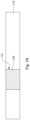
- an opening 112is formed in a dielectric layer 110 .
- the dielectric layer 110is formed over a semiconductor substrate (not shown).
- the semiconductor substratemay be a semiconductor material and may include known structures including a graded layer or a buried oxide, for example.
- the substrateincludes bulk silicon that may be undoped or doped (e.g., p-type, n-type, or a combination thereof).
- Other materials that are suitable for semiconductor device formationmay be used.
- Other materials, such as germanium, quartz, sapphire, and glasscould alternatively be used for the substrate.
- the substratemay be an active layer of a semiconductor-on-insulator (SOI) substrate or a multi-layered structure such as a silicon-germanium layer formed on a bulk silicon layer.
- SOIsemiconductor-on-insulator
- Integrated circuitssuch as PMOS and NMOS transistors (not shown) may be formed on the top surface of the substrate.
- the dielectric layer 110is an inter-metal dielectric (IMD) having a low dielectric constant value (k value), for example, lower than about 3.5.
- IMDinter-metal dielectric
- the dielectric layer 110may comprise dielectric materials, such as silicon oxide, silicon nitride, silicon oxy-nitride, or other suitable material.
- the opening 112may be formed, for example, by forming a patterned photoresist layer (not shown) over the dielectric layer 110 and using a dry etch processing step to remove portions of the dielectric layer 110 to define the opening 112 by using the patterned photoresist layer (not shown) as a mask.
- a dry etch processing stepmay be used.
- the patterned photoresist layer (not shown)is removed by, for example, a photolithographic removal process.
- a conductive feature 120is formed in the opening 112 .
- the process of forming the conductive feature 120includes forming a conductive layer filling the opening 112 and on the dielectric layer 110 , and then removing the excess portion of the conductive layer (not shown) that has accumulated over the surface of the dielectric layer 110 , such that the conductive feature 120 is present in the opening 112 .
- the conductive layercan be a metal layer.
- the material of conductive layermay include copper or copper alloys, or other suitable conductive materials, such as silver, gold, tungsten, aluminum, and the like.
- the conductive layercan be formed by a deposition process.
- the removing processcan be any suitable planarization process, such as a chemical mechanical polishing (CMP).
- CMPchemical mechanical polishing
- the chemical mechanical processis performed to level the surface of conductive feature 120 and the dielectric layer 110 .
- the conductive feature 120can be a conductive line, which may be the first or any subsequent metal interconnect level of the semiconductor device.
- a diffusion barrier layer(not shown) is optionally deposited over inside surfaces of opening 112 and over the surface of the dielectric layer 110 before the conductive layer is formed.
- the diffusion barrier layercan be deposited using methods of such as CVD or PVD, to a thickness of between about 50 and 300 angstrom.
- the metal barrier material of the diffusion barrier layer 122includes Ta, TaN or TiN.
- At least one etch stop layeris formed on the dielectric layer 110 and on the conductive feature 120 .
- a lower etch stop layer 130is formed on the dielectric layer 110 and on the conductive feature 120 , and then an upper etch stop layer 140 is optionally formed on the lower etch stop layer 130 .
- the lower etch stop layer 130 and the upper etch stop layer 140are made of different material.
- the lower etch stop layer 130 and the upper etch stop layer 140can be formed by a series of deposition processes.
- the deposition processcan be such as chemical vapor deposition (CVD), physical vapor deposition (PVD), atomic layer deposition (ALD), remote plasma enhanced chemical vapor deposition (RPECVD), liquid source misted chemical deposition (LSMCD), coating, spin-coating or another process that is adapted to form a thin film layer over the substrate.
- CVDchemical vapor deposition
- PVDphysical vapor deposition
- ALDatomic layer deposition
- RECVDremote plasma enhanced chemical vapor deposition
- LSMCDliquid source misted chemical deposition
- coatingspin-coating or another process that is adapted to form a thin film layer over the substrate.
- the lower etch stop layer 130is a low capacitance material to improve RC delay.
- the lower etch stop layer 130is an aluminum-containing layer.
- the material of the lower etch stop layer 130can be, for example, aluminum nitride, aluminum oxynitride, aluminum carbide, or combinations thereof. If depositing an aluminum nitride layer as the lower etch stop layer 130 , the layer can be formed by reactive sputtering (RS) with an aluminum target in a nitrogen atmosphere.
- RSreactive sputtering
- the lower etch stop layer 130is formed on the dielectric layer 110 and serves as an etch stop for continued, back-end-of-line (BEOL) metallization.
- the thickness of the lower etch stop layer 130is a thin layer and is in a range from 5 to 50 angstroms.
- the upper etch stop layer 140is made of material different from the lower etch stop layer 130 .
- the upper etch stop layer 140is an aluminum free layer.
- the upper etch stop layer 140may have a dielectric constant lower than about 4.0, or even lower than about 3.5, and may comprise a material selected from nitrogen doped (silicon) carbide (SiC:N, also known as NDC), oxygen doped (silicon) carbide (SiC:O, also known as ODC), and combinations thereof.
- the reaction gases (precursors)depend on the desired composition of etch stop layer, and may include silicon (Si), carbon (C), hydrogen (H), nitrogen (N), oxygen (O), boron (B), and/or the like.
- Inactive gasessuch as He, N 2 , Ar, Xe, and the like may be used as ambient gases. If ODC is to be formed, CO 2 may also be added to provide oxygen. If NDC is to be formed, NH 3 may be added to provide nitrogen.
- the thickness of the upper etch stop layer 140is in a range from 30 to 1000 angstroms.
- the upper etch stop layer 140may be formed in-situ with the formation of lower etch stop layer 130 , which means that lower etch stop layer 130 and upper etch stop layer 140 are formed in a same process chamber.
- the deposition of lower etch stop layer 130 and upper etch stop layer 140may both be performed at elevated temperatures, for example, between about 100° C. and about 500° C.
- an additional dielectric layer 150is formed on the upper etch stop layer 140 .
- the dielectric layer 150can be an inter-metal dielectric (IMD) layer.
- IMDinter-metal dielectric
- the dielectric layer 150may be a single layer or a multi-layered structure.
- the thickness of the dielectric layer 150varies with the applied technology, for example a thickness of about 1000 angstroms to about 30000 angstroms.
- One skilled in the artwill realize, however, that the dimensions recited throughout the description are merely examples, and will change if different formation technologies are used.
- the dielectric layer 150is an oxygen-containing dielectric layer.
- the dielectric layer 150may be formed of SiO 2 , carbon-doped SiO 2 , a comparatively low dielectric constant (k value) dielectric material with a k value less than about 4.0, or combinations thereof.
- the dielectric layer 150may be formed of a low-k dielectric material, an extreme low-k dielectric material, a porous low-k dielectric layer, or combinations thereof.
- low-kis intended to define a dielectric constant of a dielectric material of 3.0 or less.
- extreme low-k (ELK)”means a dielectric constant of 2.5 or less.
- porous low-krefers to a dielectric constant of a dielectric material of 2.0 or less.
- a wide variety of low-k materialsmay be employed in accordance with embodiments, for example, spin-on inorganic dielectrics, spin-on organic dielectrics, porous dielectric materials, organic polymer, organic silica glass, FSG (SiOF series material), HSQ (hydrogen silsesquioxane) series material, MSQ (methyl silsesquioxane) series material, or porous organic series material.
- the dielectric layer 150is deposited through any of a variety of techniques, such as CVD, PVD, ALD, RPECVD, LSMCD, coating, spin-coating or another process that is adapted to form a thin film layer over the substrate.
- An anti-reflective coating (ARC) layer 160 and a cap layer 170may be optionally deposited on the dielectric layer 150 .
- the anti-reflective coating layer 160can be a nitrogen free anti-reflective coating layer (NFARL), and the cap layer 170 can be a titanium nitride (TiN) layer, or a tantalum nitride (TaN) layer.
- the anti-reflective coating layer 160 and the cap layer 170can be formed by any suitable deposition process.
- the composite of the anti-reflective coating layer 160 and the cap layer 170is regarded as a barrier and anti-reflective coating (BARC) layer.
- the cap layer 170is usable as an etch stop for later processing in forming the semiconductor device.
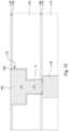
- a hole 152is formed in the structure above.
- the hole 152can be an exemplary dual damascene opening including an upper trench section 151 and a lower via-hole section 153 patterned in the structure to define a contact region in the substrate.
- the upper trench section 151 and the lower via-hole section 153may be formed using a typical lithographic with masking technologies and anisotropic etch operation (e.g. plasma etching or reactive ion etching).
- the upper trench section 151may be formed using a first masking layer (not shown) along with a suitable etching process.
- the masking layermay be a hardmask including silicon nitride formed through a process such as a CVD process, although other materials, such as oxides, oxynitrides, silicon carbide, combinations of these, or the like, and other processes, such as PECVD, LPCVD, or even silicon oxide formation followed by nitridation, may alternatively be utilized.
- the masking layermay be patterned through a suitable photolithographic process to expose those portions of the underlying layers that will be removed to form the upper trench section 151 .
- the upper trench section 151may be formed by performing a dry etching process, such as plasma etching or reactive ion etching.
- a middle etch stop layermay be optionally deposited intermediately in the dielectric layer 150 to provide a clear indicator of when to end a particular etching process. The masking layer is removed after the upper trench section 151 is formed.
- the dielectric layer 150 under the upper trench section 151is patterned to form lower via-hole section 153 under the upper trench section 151 .
- the portion of aside the predetermined position of the upper trench section 151is once again protected by another masking layer.
- the portion of the dielectric layer 150 for forming the lower via-hole section 153is exposed from the masking layer.
- the exposed portion of the dielectric layer 150is removed by a dry etching process, such as plasma etching or reactive ion etching.
- the lower via-hole section 153has higher aspect ratio than that of the upper trench section 151 , the width of the lower via-hole section 153 is smaller than the width of the upper trench section 151 .
- the masking layeris removed after the lower via-hole section 153 is formed.
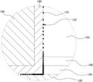
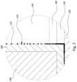
- the hole 152is formed penetrating the dielectric layer 150 , the anti-reflective coating layer 160 , the cap layer 170 , the upper etch stop layer 140 , and the lower etch stop layer 130 . Therefore, the conductive feature 120 is exposed from the hole 152 .
- the embodimentillustrates dual damascene openings in the dielectric layer 150
- the use of single damascene openings in the dielectric layer 150also provide values.
- the hole 152is formed by performing one or more dry etching process, layers above are exposed to a bombardment of ions (e.g. a plasma of reactive gases such as fluorocarbons, oxygen, chlorine). The materials of the layers are dislodged from the exposed surface and are resputtered onto the sidewall of the hole 152 .
- the lower etch stop layer 130is an aluminum-containing layer, which is a low capacitance material to improve RC delay of the interconnection structure.
- the aluminumis light and has good binding ability to the dielectric material.
- some aluminum-containing fragments 132which are from the dislodged material of the lower etch stop layer 130 , are present at the bottom portion of the sidewall of the hole 152 , such as at the bottom portion of the lower via-hole section 153 . Namely, a portion of the lower etch stop layer 130 is knocked out by the ions during the dry etching process and becomes aluminum-containing fragments 132 , and a portion of the aluminum-containing fragments 132 is adhered at the sidewall of the dielectric layer 150 and at the bottom corner of the hole 152 .
- the distribution of the aluminum-containing fragments 132 on the sidewall and the bottom corner of the hole 152is corresponding to the distance from the conductive feature 120 .
- the aluminum-containing fragments 132have greater density at the bottom portion of the sidewall of the hole 152 , and the density of the aluminum-containing fragments 132 is decreased with the increasing distance from the conductive feature 120 .
- the aluminum-containing fragments 132may have the greatest density at the corner between the dielectric layer 150 and the conductive feature 120 .
- a barrier layer 180is formed on the sidewall of the hole 152 .
- the barrier layer 180is deposited over inside surfaces of hole 152 and over the surface of the dielectric layer 150 .
- the barrier layer 180can be deposited using methods of such as CVD or PVD, to a thickness of between about 50 and 300 angstrom.
- CVDchemical vapor deposition
- PVDphysical vapor deposition
- copperhas increasingly gained acceptance and is increasingly being used for this purpose. Copper is known to have low cost and a low resistivity; copper however has a relatively large diffusion coefficient into dielectric material such as silicon dioxide and silicon.
- the barrier layer 180is utilized for preventing following deposited conductive metal, such as copper or copper alloy from diffusing into the dielectric layer 150 .
- the barrier layer 180is made of a substantially aluminum free material.
- the metal barrier material of the barrier layer 180includes Ta, TaN or TiN.
- a thin seed layeris optionally formed on the barrier layer 180 .
- the seed layerhas a thickness of about 100 angstroms to about 1000 angstroms.
- the seed layeris a metal alloy layer containing at least a main metal element, e.g., copper (Cu), and a first additive metal element, e.g., manganese (Mn).
- Cucopper
- Mnmanganese
- Ti, Nb, Cr, V, Y, Tc, Re, or the likecan be utilized as another additive metal for forming the seed layer.
- the seed layermay be deposited by using physical vapor deposition (PVD), chemical vapor deposition (CVD), plasma enhanced CVD (PECVD), low pressure CVD (LPCVD), or other well-known deposition techniques.
- the seed layeris utilized for improving the quantity of the following deposition process.
- the hole 152such as the dual damascene opening, is filled with a conductive material.
- An electrochemical copper deposition (ECD)is carried out to form a conductive layer 190 on the barrier layer 180 (or on the seed layer) and fill the hole 152 .
- the hole 152 including the upper trench section 151 and the lower via-hole section 153is filled with the conductive material.
- the conductive layer 190can be a metal layer.
- the material of conductive layer 190may include copper or copper alloys, or other suitable conductive materials, such as silver, gold, tungsten, and the like.
- the conductive layer 190is made of a substantially aluminum free material.
- the barrier layer 180may function as a protector to prevent the conductive layer 190 diffusing into the dielectric layer 150 .
- the electrochemical copper depositionhas been adopted for copper metallization because of its larger grain size (good electromigration) and high deposition rates.
- the electrochemical copper deposition processsuch as electro-chemical plating, is a wet process and causes void formation in the hole 152 .
- the electrolytecan also be trapped in the voids causing reliability problems.
- a thermal treatmentfor example an annealing process, is performed on above structure.
- the step of thermal treatmentis provided at the time immediately after the formation of the conductive layer 190 .
- the step of thermal treatmentis provided at the time immediately after the step of CMP of removing the excess portions of the conductive layer 190 outside the hole 152 .
- the temperature of the annealing processcan be ranged from about 50 to 400° C.
- the duration of the annealing processmay be ranged from about 5 to 60 minutes.
- a chemical mechanical polishing processis performed to remove the excess portions of the conductive layer 190 , and the barrier layer 180 outside the hole 152 , thus exposing the top surface of the cap layer 170 and achieving a planarized surface.
- the remaining conductive layer 190 in the hole 152is regarded as a conductor (referring as conductor 190 hereafter).
- the hole 152 and conductor 190 thereinis regarded as a conductive via for interconnection to the conductive feature 120 .
- the aluminum-containing fragments 132are present at least at a bottom corner of the conductive via.
- the sidewall of the conductive viahas a bottom portion and a middle portion, the bottom portion is closer to the lower etch stop layer 130 than the middle portion, and the density of the aluminum-containing fragments 132 on the bottom portion of the sidewall of the conductive via is greater than that on the middle portion of the sidewall of the conductive via.
- FIG. 2is an enlarged view of the portion A in FIG. 1 F , in accordance with some embodiments of the disclosure.
- the conductor 190 after the annealing and planarization, e.g., chemical mechanical polishing,has a lower resistance and better electromigration lifetimes.
- the electrochemical copper deposition processmay form void in the conductor 190 , but also the anneal process results in void formation.
- the stresses during the anneal processdeform the conductor 190 and cause additional void formed at the interface between the conductor 190 and the barrier layer 180 .
- the existence of the voidsmay reduce the volume of the conductive material in the hole 152 thereby increasing the resistance of the conductor 190 , which may also increase the RC delay of the semiconductor device.
- the etch stop layer for BOELsuch as the lower etch stop layer 130 is made of low capacitance material which may improve RC delay. Since the via is formed by dry etching process, a portion of the etch stop layer is bombed by ions and is dislodged from the exposed surface and may adhere on the sidewall and at the corner of the via.
- the low capacitance material for the etch stop layeris an aluminum-containing material, such as aluminum nitride, aluminum oxynitride, aluminum carbide, or combinations thereof. The aluminum is light and has good binding ability to the dielectric material.
- some aluminum-containing fragments 132which are from the dislodged material of the lower etch stop layer 130 , are adhered at the bottom portion of the sidewall and at the bottom corner of the hole 152 .
- the aluminum-containing fragments 132may serve as an additional barrier to prevent the conductor 190 from escaping.
- an interconnection structureincludes a first dielectric layer, a bottom conductive feature present in the first dielectric layer, a second dielectric layer present on the first dielectric layer and having a hole therein, an upper conductor present in the hole and electrically connected to the bottom conductive feature, and a plurality of aluminum-containing fragments present at least partially on at least one sidewall of the hole, wherein a density of the aluminum-containing fragments at the bottom of the sidewall of the hole is greater than that in the middle of the sidewall of the hole.
- an interconnection structureincludes a first dielectric layer, a bottom conductive feature present in the first dielectric layer, a second dielectric layer present on the first dielectric layer, an aluminum-containing etch stop layer present between the first dielectric layer and the second dielectric layer, an upper conductive via present at least in the second dielectric layer and electrically connected to the bottom conductive feature, and at least one aluminum-containing fragment present at least at a bottom corner of the upper conductive via.
- a method of manufacturing an interconnection structureincludes forming a bottom conductive feature in a first dielectric layer; forming an aluminum-containing etch stop layer on the bottom conductive feature and the first dielectric layer; forming a second dielectric layer on the aluminum-containing etch stop layer; and etching the second dielectric layer and the aluminum-containing etch stop layer to form a hole in the second dielectric layer and the aluminum-containing etch stop layer, wherein the bottom conductive feature is at least partially exposed by the hole, and the etching the aluminum-containing etch stop layer resputters at least one aluminum-containing fragment onto at least one sidewall of the hole.
Landscapes
- Engineering & Computer Science (AREA)
- Physics & Mathematics (AREA)
- Condensed Matter Physics & Semiconductors (AREA)
- General Physics & Mathematics (AREA)
- Computer Hardware Design (AREA)
- Microelectronics & Electronic Packaging (AREA)
- Power Engineering (AREA)
- Manufacturing & Machinery (AREA)
- Internal Circuitry In Semiconductor Integrated Circuit Devices (AREA)
Abstract
Description
Claims (20)
Priority Applications (1)
| Application Number | Priority Date | Filing Date | Title |
|---|---|---|---|
| US16/851,191US12315761B2 (en) | 2015-12-21 | 2020-04-17 | Interconnection structure and manufacturing method thereof |
Applications Claiming Priority (5)
| Application Number | Priority Date | Filing Date | Title |
|---|---|---|---|
| US201562270468P | 2015-12-21 | 2015-12-21 | |
| US15/145,369US9837306B2 (en) | 2015-12-21 | 2016-05-03 | Interconnection structure and manufacturing method thereof |
| US15/830,142US10510588B2 (en) | 2015-12-21 | 2017-12-04 | Interconnection structure and manufacturing method thereof |
| US16/715,083US10854508B2 (en) | 2015-12-21 | 2019-12-16 | Interconnection structure and manufacturing method thereof |
| US16/851,191US12315761B2 (en) | 2015-12-21 | 2020-04-17 | Interconnection structure and manufacturing method thereof |
Related Parent Applications (1)
| Application Number | Title | Priority Date | Filing Date |
|---|---|---|---|
| US16/715,083ContinuationUS10854508B2 (en) | 2015-12-21 | 2019-12-16 | Interconnection structure and manufacturing method thereof |
Publications (2)
| Publication Number | Publication Date |
|---|---|
| US20200251383A1 US20200251383A1 (en) | 2020-08-06 |
| US12315761B2true US12315761B2 (en) | 2025-05-27 |
Family
ID=59066379
Family Applications (4)
| Application Number | Title | Priority Date | Filing Date |
|---|---|---|---|
| US15/145,369ActiveUS9837306B2 (en) | 2015-12-21 | 2016-05-03 | Interconnection structure and manufacturing method thereof |
| US15/830,142ActiveUS10510588B2 (en) | 2015-12-21 | 2017-12-04 | Interconnection structure and manufacturing method thereof |
| US16/715,083ActiveUS10854508B2 (en) | 2015-12-21 | 2019-12-16 | Interconnection structure and manufacturing method thereof |
| US16/851,191Active2036-12-22US12315761B2 (en) | 2015-12-21 | 2020-04-17 | Interconnection structure and manufacturing method thereof |
Family Applications Before (3)
| Application Number | Title | Priority Date | Filing Date |
|---|---|---|---|
| US15/145,369ActiveUS9837306B2 (en) | 2015-12-21 | 2016-05-03 | Interconnection structure and manufacturing method thereof |
| US15/830,142ActiveUS10510588B2 (en) | 2015-12-21 | 2017-12-04 | Interconnection structure and manufacturing method thereof |
| US16/715,083ActiveUS10854508B2 (en) | 2015-12-21 | 2019-12-16 | Interconnection structure and manufacturing method thereof |
Country Status (3)
| Country | Link |
|---|---|
| US (4) | US9837306B2 (en) |
| CN (1) | CN106898595B (en) |
| TW (1) | TWI611545B (en) |
Families Citing this family (16)
| Publication number | Priority date | Publication date | Assignee | Title |
|---|---|---|---|---|
| US9837306B2 (en)* | 2015-12-21 | 2017-12-05 | Taiwan Semiconductor Manufacturing Co., Ltd. | Interconnection structure and manufacturing method thereof |
| US10522468B2 (en)* | 2017-07-31 | 2019-12-31 | Taiwan Semiconductor Manufacturing Company, Ltd. | Interconnect structure and method |
| US12087692B2 (en)* | 2017-09-28 | 2024-09-10 | Taiwan Semiconductor Manufacturing Co., Ltd. | Hardened interlayer dielectric layer |
| US10790362B2 (en) | 2017-11-30 | 2020-09-29 | Taiwan Semiconductor Manufacturing Company Ltd. | Semiconductor structure and manufacturing method of the same |
| US11069526B2 (en)* | 2018-06-27 | 2021-07-20 | Taiwan Semiconductor Manufacturing Co., Ltd. | Using a self-assembly layer to facilitate selective formation of an etching stop layer |
| CN110875320B (en) | 2018-08-29 | 2022-02-11 | 中芯国际集成电路制造(上海)有限公司 | Semiconductor device and method of forming the same |
| US10978337B2 (en)* | 2018-09-18 | 2021-04-13 | Taiwan Semiconductor Manufacturing Co., Ltd. | Aluminum-containing layers and methods of forming the same |
| US11322397B2 (en)* | 2018-10-30 | 2022-05-03 | Taiwan Semiconductor Manufacturing Co., Ltd. | Method of manufacturing semiconductor devices including formation of adhesion enhancement layer |
| US11502001B2 (en)* | 2018-10-31 | 2022-11-15 | Taiwan Semiconductor Manufacturing Company, Ltd. | Semiconductor device with self-aligned vias |
| US20200176379A1 (en)* | 2018-11-30 | 2020-06-04 | Taiwan Semiconductor Manufacturing Co., Ltd. | Metal filament vias for interconnect structure |
| US11037822B2 (en) | 2019-05-08 | 2021-06-15 | International Business Machines Corporation | Svia using a single damascene interconnect |
| US11482454B2 (en)* | 2021-02-17 | 2022-10-25 | Tokyo Electron Limited | Methods for forming self-aligned contacts using spin-on silicon carbide |
| KR20220153175A (en) | 2021-05-10 | 2022-11-18 | 삼성전자주식회사 | Semiconductor device |
| US20230299000A1 (en)* | 2022-03-17 | 2023-09-21 | International Business Machines Corporation | Method and structure for forming landing for backside power distribution network |
| US20230335498A1 (en)* | 2022-04-18 | 2023-10-19 | Taiwan Semiconductor Manufacturing Company, Ltd. | Interconnection structure and methods of forming the same |
| US12308310B2 (en)* | 2022-05-05 | 2025-05-20 | Nanya Technology Corporation | Method for forming semiconductor interconnection structure against stress migration |
Citations (34)
| Publication number | Priority date | Publication date | Assignee | Title |
|---|---|---|---|---|
| US5525542A (en) | 1995-02-24 | 1996-06-11 | Motorola, Inc. | Method for making a semiconductor device having anti-reflective coating |
| US5702981A (en)* | 1995-09-29 | 1997-12-30 | Maniar; Papu D. | Method for forming a via in a semiconductor device |
| US6372653B1 (en) | 2000-07-07 | 2002-04-16 | Taiwan Semiconductor Manufacturing Co., Ltd | Method of forming dual damascene structure |
| US20020140103A1 (en)* | 2001-03-28 | 2002-10-03 | Grant Kloster | Structure in a microelectronic device including a bi-layer for a diffusion barrier and an etch-stop layer |
| US6492272B1 (en) | 2001-02-15 | 2002-12-10 | Advanced Micro Devices, Inc. | Carrier gas modification for use in plasma ashing of photoresist |
| US6586842B1 (en) | 2001-02-28 | 2003-07-01 | Advanced Micro Devices, Inc. | Dual damascene integration scheme for preventing copper contamination of dielectric layer |
| US20040002212A1 (en)* | 2002-06-29 | 2004-01-01 | Hynix Semiconductor Inc. | Method for forming copper metal line in semiconductor device |
| US20040137709A1 (en)* | 2003-01-09 | 2004-07-15 | Chartered Semiconductor Manufacturing Ltd. | Metal barrier cap fabrication by polymer lift-off |
| US20040180538A1 (en) | 2001-07-14 | 2004-09-16 | Paul Rich | Method for producing a copper connection |
| US20050095869A1 (en) | 2003-11-05 | 2005-05-05 | Hun-Jan Tao | Low K dielectric surface damage control |
| US20050266683A1 (en) | 1998-07-06 | 2005-12-01 | Lee Wai M | Remover compositions for dual damascene system |
| US20060024941A1 (en) | 2004-07-30 | 2006-02-02 | Samsung Electronics Co., Ltd. | Method of forming metal interconnect of semiconductor device |
| US20080096290A1 (en) | 2006-10-19 | 2008-04-24 | Smith Kenneth H | Magnetic tunnel junction memory and method with etch-stop layer |
| US20090142931A1 (en) | 2007-11-29 | 2009-06-04 | Chieh-Ju Wang | Cleaning method following opening etch |
| US20100013098A1 (en) | 2004-12-01 | 2010-01-21 | Koninklijke Philips Electronics N.V. | Method of forming an interconnect structure on an integrated circuit die |
| CN101842744A (en) | 2007-11-01 | 2010-09-22 | 爱发科成膜株式会社 | Half-tone mask, half-tone mask blank and method for manufacturing half-tone mask |
| US20100252930A1 (en) | 2009-04-01 | 2010-10-07 | Taiwan Semiconductor Manufacturing Company, Ltd. | Method for Improving Performance of Etch Stop Layer |
| US20110223759A1 (en)* | 2010-03-15 | 2011-09-15 | Taiwan Semiconductor Manufacturing Company, Ltd. | Low-k Cu Barriers in Damascene Interconnect Structures |
| US20130214391A1 (en) | 2012-02-17 | 2013-08-22 | International Business Machines Corporation | Lateral-Dimension-Reducing Metallic Hard Mask Etch |
| US20140190933A1 (en) | 2012-04-26 | 2014-07-10 | Everspin Technologies, Inc. | Method of manufacturing a magnetoresistive device |
| US20140212993A1 (en) | 2013-01-31 | 2014-07-31 | Everspin Technologies, Inc. | Method of manufacturing a magnetoresistive device |
| CN104051256A (en) | 2013-03-14 | 2014-09-17 | 台湾积体电路制造股份有限公司 | Semiconductor Devices and Methods of Manufacture Thereof |
| US20140264895A1 (en) | 2013-03-14 | 2014-09-18 | Taiwan Semiconductor Manufacturing Company, Ltd. | Semiconductor Devices and Methods of Manufacture Thereof |
| US20140264641A1 (en) | 2013-03-14 | 2014-09-18 | Globalfoundries Inc. | Semiconductor device comprising contact structures with protection layers formed on sidewalls of contact etch stop layers |
| TWM489420U (en) | 2014-02-21 | 2014-11-01 | Ya-Ling Zhang | Power generation device capable of reducing occupation area |
| US20150048488A1 (en) | 2013-08-15 | 2015-02-19 | Taiwan Semiconductor Manufacturing Company, Ltd. | Semiconductor Devices, Methods of Manufacture Thereof, and Inter-metal Dielectric (IMD) Structures |
| TW201532226A (en) | 2013-12-30 | 2015-08-16 | Taiwan Semiconductor Mfg Co Ltd | An interconnect structure and method of forming the same |
| US20160111325A1 (en) | 2014-10-17 | 2016-04-21 | Taiwan Semiconductor Manufacturing Company, Ltd. | Etch stop layer in integrated circuits |
| US20160133512A1 (en)* | 2014-11-12 | 2016-05-12 | Woojin Lee | Method of manufacturing semiconductor device using a plurality of etch stop layers |
| US20160240428A1 (en) | 2015-02-12 | 2016-08-18 | Taiwan Semiconductor Manufacturing Company, Ltd. | Method of Forming an Interconnect Structure Having an Air Gap and Structure Thereof |
| US9515021B1 (en) | 2015-10-20 | 2016-12-06 | Taiwan Semiconductor Manufacturing Co., Ltd. | Semiconductor structure and method of forming the same |
| US20160372413A1 (en) | 2015-06-17 | 2016-12-22 | Globalfoundries Inc. | Unique bi-layer etch stop to protect conductive structures during a metal hard mask removal process and methods of using same |
| US20170162430A1 (en) | 2015-12-03 | 2017-06-08 | GlobalFoundries, Inc. | Methods for producing integrated circuits with air gaps and integrated circuits produced from such methods |
| US9837306B2 (en) | 2015-12-21 | 2017-12-05 | Taiwan Semiconductor Manufacturing Co., Ltd. | Interconnection structure and manufacturing method thereof |
- 2016
- 2016-05-03USUS15/145,369patent/US9837306B2/enactiveActive
- 2016-08-24TWTW105127113Apatent/TWI611545B/enactive
- 2016-09-07CNCN201610806487.1Apatent/CN106898595B/enactiveActive
- 2017
- 2017-12-04USUS15/830,142patent/US10510588B2/enactiveActive
- 2019
- 2019-12-16USUS16/715,083patent/US10854508B2/enactiveActive
- 2020
- 2020-04-17USUS16/851,191patent/US12315761B2/enactiveActive
Patent Citations (40)
| Publication number | Priority date | Publication date | Assignee | Title |
|---|---|---|---|---|
| US5525542A (en) | 1995-02-24 | 1996-06-11 | Motorola, Inc. | Method for making a semiconductor device having anti-reflective coating |
| US5702981A (en)* | 1995-09-29 | 1997-12-30 | Maniar; Papu D. | Method for forming a via in a semiconductor device |
| US20050266683A1 (en) | 1998-07-06 | 2005-12-01 | Lee Wai M | Remover compositions for dual damascene system |
| US6372653B1 (en) | 2000-07-07 | 2002-04-16 | Taiwan Semiconductor Manufacturing Co., Ltd | Method of forming dual damascene structure |
| US6492272B1 (en) | 2001-02-15 | 2002-12-10 | Advanced Micro Devices, Inc. | Carrier gas modification for use in plasma ashing of photoresist |
| US6586842B1 (en) | 2001-02-28 | 2003-07-01 | Advanced Micro Devices, Inc. | Dual damascene integration scheme for preventing copper contamination of dielectric layer |
| US20020140103A1 (en)* | 2001-03-28 | 2002-10-03 | Grant Kloster | Structure in a microelectronic device including a bi-layer for a diffusion barrier and an etch-stop layer |
| US20040180538A1 (en) | 2001-07-14 | 2004-09-16 | Paul Rich | Method for producing a copper connection |
| US20040002212A1 (en)* | 2002-06-29 | 2004-01-01 | Hynix Semiconductor Inc. | Method for forming copper metal line in semiconductor device |
| US20040137709A1 (en)* | 2003-01-09 | 2004-07-15 | Chartered Semiconductor Manufacturing Ltd. | Metal barrier cap fabrication by polymer lift-off |
| US20050095869A1 (en) | 2003-11-05 | 2005-05-05 | Hun-Jan Tao | Low K dielectric surface damage control |
| US20060024941A1 (en) | 2004-07-30 | 2006-02-02 | Samsung Electronics Co., Ltd. | Method of forming metal interconnect of semiconductor device |
| US20100013098A1 (en) | 2004-12-01 | 2010-01-21 | Koninklijke Philips Electronics N.V. | Method of forming an interconnect structure on an integrated circuit die |
| US20080096290A1 (en) | 2006-10-19 | 2008-04-24 | Smith Kenneth H | Magnetic tunnel junction memory and method with etch-stop layer |
| CN101842744A (en) | 2007-11-01 | 2010-09-22 | 爱发科成膜株式会社 | Half-tone mask, half-tone mask blank and method for manufacturing half-tone mask |
| US20100261096A1 (en) | 2007-11-01 | 2010-10-14 | Ulvac Coating Corporation | Half-tone mask, half-tone mask blank and method for manufacturing half-tone mask |
| US8216745B2 (en) | 2007-11-01 | 2012-07-10 | Ulvac Coating Corporation | Half-tone mask, half-tone mask blank and method for manufacturing half-tone mask |
| US20090142931A1 (en) | 2007-11-29 | 2009-06-04 | Chieh-Ju Wang | Cleaning method following opening etch |
| US20100252930A1 (en) | 2009-04-01 | 2010-10-07 | Taiwan Semiconductor Manufacturing Company, Ltd. | Method for Improving Performance of Etch Stop Layer |
| CN101859727A (en) | 2009-04-01 | 2010-10-13 | 台湾积体电路制造股份有限公司 | Interconnect structure |
| US20120256324A1 (en) | 2009-04-01 | 2012-10-11 | Taiwan Semiconductor Manufacturing Company, Ltd. | Method for Improving Performance of Etch Stop Layer |
| CN102194739A (en) | 2010-03-15 | 2011-09-21 | 台湾积体电路制造股份有限公司 | Formation method of interconnection structure |
| US20110223759A1 (en)* | 2010-03-15 | 2011-09-15 | Taiwan Semiconductor Manufacturing Company, Ltd. | Low-k Cu Barriers in Damascene Interconnect Structures |
| US20130214391A1 (en) | 2012-02-17 | 2013-08-22 | International Business Machines Corporation | Lateral-Dimension-Reducing Metallic Hard Mask Etch |
| US20140190933A1 (en) | 2012-04-26 | 2014-07-10 | Everspin Technologies, Inc. | Method of manufacturing a magnetoresistive device |
| US20140212993A1 (en) | 2013-01-31 | 2014-07-31 | Everspin Technologies, Inc. | Method of manufacturing a magnetoresistive device |
| CN104051256A (en) | 2013-03-14 | 2014-09-17 | 台湾积体电路制造股份有限公司 | Semiconductor Devices and Methods of Manufacture Thereof |
| US20140264895A1 (en) | 2013-03-14 | 2014-09-18 | Taiwan Semiconductor Manufacturing Company, Ltd. | Semiconductor Devices and Methods of Manufacture Thereof |
| US20140264641A1 (en) | 2013-03-14 | 2014-09-18 | Globalfoundries Inc. | Semiconductor device comprising contact structures with protection layers formed on sidewalls of contact etch stop layers |
| US20150048488A1 (en) | 2013-08-15 | 2015-02-19 | Taiwan Semiconductor Manufacturing Company, Ltd. | Semiconductor Devices, Methods of Manufacture Thereof, and Inter-metal Dielectric (IMD) Structures |
| TW201532226A (en) | 2013-12-30 | 2015-08-16 | Taiwan Semiconductor Mfg Co Ltd | An interconnect structure and method of forming the same |
| TWM489420U (en) | 2014-02-21 | 2014-11-01 | Ya-Ling Zhang | Power generation device capable of reducing occupation area |
| US20160111325A1 (en) | 2014-10-17 | 2016-04-21 | Taiwan Semiconductor Manufacturing Company, Ltd. | Etch stop layer in integrated circuits |
| US20160133512A1 (en)* | 2014-11-12 | 2016-05-12 | Woojin Lee | Method of manufacturing semiconductor device using a plurality of etch stop layers |
| US20160240428A1 (en) | 2015-02-12 | 2016-08-18 | Taiwan Semiconductor Manufacturing Company, Ltd. | Method of Forming an Interconnect Structure Having an Air Gap and Structure Thereof |
| US20160372413A1 (en) | 2015-06-17 | 2016-12-22 | Globalfoundries Inc. | Unique bi-layer etch stop to protect conductive structures during a metal hard mask removal process and methods of using same |
| US9515021B1 (en) | 2015-10-20 | 2016-12-06 | Taiwan Semiconductor Manufacturing Co., Ltd. | Semiconductor structure and method of forming the same |
| US20170162430A1 (en) | 2015-12-03 | 2017-06-08 | GlobalFoundries, Inc. | Methods for producing integrated circuits with air gaps and integrated circuits produced from such methods |
| US9837306B2 (en) | 2015-12-21 | 2017-12-05 | Taiwan Semiconductor Manufacturing Co., Ltd. | Interconnection structure and manufacturing method thereof |
| US10510588B2 (en) | 2015-12-21 | 2019-12-17 | Taiwan Semiconductor Manufacturing Company Limited | Interconnection structure and manufacturing method thereof |
Also Published As
| Publication number | Publication date |
|---|---|
| US20180102283A1 (en) | 2018-04-12 |
| CN106898595A (en) | 2017-06-27 |
| US20200118869A1 (en) | 2020-04-16 |
| CN106898595B (en) | 2020-02-07 |
| US20200251383A1 (en) | 2020-08-06 |
| TWI611545B (en) | 2018-01-11 |
| US9837306B2 (en) | 2017-12-05 |
| US20170178954A1 (en) | 2017-06-22 |
| US10510588B2 (en) | 2019-12-17 |
| TW201724436A (en) | 2017-07-01 |
| US10854508B2 (en) | 2020-12-01 |
Similar Documents
| Publication | Publication Date | Title |
|---|---|---|
| US12315761B2 (en) | Interconnection structure and manufacturing method thereof | |
| US11088020B2 (en) | Structure and formation method of interconnection structure of semiconductor device | |
| US11177167B2 (en) | Ultrathin multilayer metal alloy liner for nano Cu interconnects | |
| US8134234B2 (en) | Application of Mn for damage restoration after etchback | |
| US8361900B2 (en) | Barrier layer for copper interconnect | |
| US8288276B2 (en) | Method of forming an interconnect structure including a metallic interfacial layer located at a bottom via portion | |
| US7772119B2 (en) | Dual liner capping layer interconnect structure | |
| US20070059919A1 (en) | Method of manufacturing semiconductor device | |
| US9824918B2 (en) | Method for electromigration and adhesion using two selective deposition | |
| US10665541B2 (en) | Biconvex low resistance metal wire | |
| US9553017B2 (en) | Methods for fabricating integrated circuits including back-end-of-the-line interconnect structures | |
| US10535560B2 (en) | Interconnection structure of semiconductor device | |
| US10177091B2 (en) | Interconnect structure and method of forming | |
| US20060118955A1 (en) | Robust copper interconnection structure and fabrication method thereof | |
| US20070155186A1 (en) | OPTIMIZED SiCN CAPPING LAYER |
Legal Events
| Date | Code | Title | Description |
|---|---|---|---|
| FEPP | Fee payment procedure | Free format text:ENTITY STATUS SET TO UNDISCOUNTED (ORIGINAL EVENT CODE: BIG.); ENTITY STATUS OF PATENT OWNER: LARGE ENTITY | |
| STPP | Information on status: patent application and granting procedure in general | Free format text:DOCKETED NEW CASE - READY FOR EXAMINATION | |
| STPP | Information on status: patent application and granting procedure in general | Free format text:NON FINAL ACTION MAILED | |
| STPP | Information on status: patent application and granting procedure in general | Free format text:RESPONSE TO NON-FINAL OFFICE ACTION ENTERED AND FORWARDED TO EXAMINER | |
| STPP | Information on status: patent application and granting procedure in general | Free format text:FINAL REJECTION MAILED | |
| STCV | Information on status: appeal procedure | Free format text:NOTICE OF APPEAL FILED | |
| STCV | Information on status: appeal procedure | Free format text:APPEAL BRIEF (OR SUPPLEMENTAL BRIEF) ENTERED AND FORWARDED TO EXAMINER | |
| STCV | Information on status: appeal procedure | Free format text:EXAMINER'S ANSWER TO APPEAL BRIEF MAILED | |
| STCV | Information on status: appeal procedure | Free format text:REPLY BRIEF FILED AND FORWARDED TO BPAI | |
| STCV | Information on status: appeal procedure | Free format text:ON APPEAL -- AWAITING DECISION BY THE BOARD OF APPEALS | |
| STCV | Information on status: appeal procedure | Free format text:BOARD OF APPEALS DECISION RENDERED | |
| STPP | Information on status: patent application and granting procedure in general | Free format text:DOCKETED NEW CASE - READY FOR EXAMINATION | |
| STPP | Information on status: patent application and granting procedure in general | Free format text:NOTICE OF ALLOWANCE MAILED -- APPLICATION RECEIVED IN OFFICE OF PUBLICATIONS | |
| STCF | Information on status: patent grant | Free format text:PATENTED CASE |