US12308826B2 - Bandpass filters using transversely-excited film bulk acoustic resonators - Google Patents
Bandpass filters using transversely-excited film bulk acoustic resonatorsDownload PDFInfo
- Publication number
- US12308826B2 US12308826B2US17/407,186US202117407186AUS12308826B2US 12308826 B2US12308826 B2US 12308826B2US 202117407186 AUS202117407186 AUS 202117407186AUS 12308826 B2US12308826 B2US 12308826B2
- Authority
- US
- United States
- Prior art keywords
- capacitor
- resonators
- bandpass filter
- resonance
- shunt
- Prior art date
- Legal status (The legal status is an assumption and is not a legal conclusion. Google has not performed a legal analysis and makes no representation as to the accuracy of the status listed.)
- Active, expires
Links
Images


Classifications
- H—ELECTRICITY
- H03—ELECTRONIC CIRCUITRY
- H03H—IMPEDANCE NETWORKS, e.g. RESONANT CIRCUITS; RESONATORS
- H03H9/00—Networks comprising electromechanical or electro-acoustic elements; Electromechanical resonators
- H03H9/02—Details
- H03H9/02228—Guided bulk acoustic wave devices or Lamb wave devices having interdigital transducers situated in parallel planes on either side of a piezoelectric layer
- H—ELECTRICITY
- H03—ELECTRONIC CIRCUITRY
- H03H—IMPEDANCE NETWORKS, e.g. RESONANT CIRCUITS; RESONATORS
- H03H9/00—Networks comprising electromechanical or electro-acoustic elements; Electromechanical resonators
- H03H9/15—Constructional features of resonators consisting of piezoelectric or electrostrictive material
- H03H9/17—Constructional features of resonators consisting of piezoelectric or electrostrictive material having a single resonator
- H03H9/171—Constructional features of resonators consisting of piezoelectric or electrostrictive material having a single resonator implemented with thin-film techniques, i.e. of the film bulk acoustic resonator [FBAR] type
- H03H9/172—Means for mounting on a substrate, i.e. means constituting the material interface confining the waves to a volume
- H03H9/174—Membranes
- H—ELECTRICITY
- H03—ELECTRONIC CIRCUITRY
- H03H—IMPEDANCE NETWORKS, e.g. RESONANT CIRCUITS; RESONATORS
- H03H9/00—Networks comprising electromechanical or electro-acoustic elements; Electromechanical resonators
- H03H9/15—Constructional features of resonators consisting of piezoelectric or electrostrictive material
- H03H9/205—Constructional features of resonators consisting of piezoelectric or electrostrictive material having multiple resonators
- H—ELECTRICITY
- H03—ELECTRONIC CIRCUITRY
- H03H—IMPEDANCE NETWORKS, e.g. RESONANT CIRCUITS; RESONATORS
- H03H9/00—Networks comprising electromechanical or electro-acoustic elements; Electromechanical resonators
- H03H9/46—Filters
- H03H9/54—Filters comprising resonators of piezoelectric or electrostrictive material
- H03H9/542—Filters comprising resonators of piezoelectric or electrostrictive material including passive elements
- H—ELECTRICITY
- H03—ELECTRONIC CIRCUITRY
- H03H—IMPEDANCE NETWORKS, e.g. RESONANT CIRCUITS; RESONATORS
- H03H9/00—Networks comprising electromechanical or electro-acoustic elements; Electromechanical resonators
- H03H9/46—Filters
- H03H9/54—Filters comprising resonators of piezoelectric or electrostrictive material
- H03H9/56—Monolithic crystal filters
- H03H9/566—Electric coupling means therefor
- H03H9/568—Electric coupling means therefor consisting of a ladder configuration
Definitions
- This disclosurerelates to radio frequency filters using acoustic wave resonators, and specifically to filters for use in communications equipment.
- a radio frequency (RF) filteris a two-port device configured to pass some frequencies and to stop other frequencies, where “pass” means transmit with relatively low signal loss and “stop” means block or substantially attenuate.
- the range of frequencies passed by a filteris referred to as the “pass-band” of the filter.
- the range of frequencies stopped by such a filteris referred to as the “stop-band” of the filter.
- a typical RF filterhas at least one pass-band and at least one stop-band. Specific requirements on a pass-band or stop-band depend on the application.
- a “pass-band”may be defined as a frequency range where the insertion loss of a filter is better than a defined value such as 1 dB, 2 dB, or 3 dB.
- a “stop-band”may be defined as a frequency range where the rejection of a filter is greater than a defined value such as 20 dB, 30 dB, 40 dB, or greater depending on application.
- RF filtersare used in communications systems where information is transmitted over wireless links.
- RF filtersmay be found in the RF front-ends of cellular base stations, mobile telephone and computing devices, satellite transceivers and ground stations, IoT (Internet of Things) devices, laptop computers and tablets, fixed point radio links, and other communications systems.
- IoTInternet of Things
- RF filtersare also used in radar and electronic and information warfare systems.
- RF filterstypically require many design trade-offs to achieve, for each specific application, the best compromise between performance parameters such as insertion loss, rejection, isolation, power handling, linearity, size and cost. Specific design and manufacturing methods and enhancements can benefit simultaneously one or several of these requirements.
- High performance RF filters for present communication systemscommonly incorporate acoustic wave resonators including surface acoustic wave (SAW) resonators, bulk acoustic wave (BAW) resonators, film bulk acoustic wave resonators (FBAR), and other types of acoustic resonators.
- SAWsurface acoustic wave
- BAWbulk acoustic wave
- FBARfilm bulk acoustic wave resonators
- these existing technologiesare not well-suited for use at the higher frequencies and bandwidths proposed for future communications networks.
- Radio access technology for mobile telephone networkshas been standardized by the 3GPP (3rd Generation Partnership Project).
- Radio access technology for 5th generation (5G) mobile networksis defined in the 5G NR (new radio) standard.
- the 5G NR standarddefines several new communications bands. Two of these new communications bands are n77, which uses the frequency range from 3300 MHz to 4200 MHZ, and n79, which uses the frequency range from 4400 MHz to 5000 MHz.
- Both band n77 and band n79use time-division duplexing (TDD), such that a communications device operating in band n77 and/or band n79 uses the same frequencies for both uplink and downlink transmissions.
- TDDtime-division duplexing
- Bandpass filters for bands n77 and n79must be capable of handling the transmit power of the communications device.
- WiFi bands at 5 GHz and 6 GHzalso require high frequency and wide bandwidth.
- the 5G NR standardalso defines millimeter wave communication bands with frequencies between 24.25 GHz and 40 GHz.
- the Transversely-Excited Film Bulk Acoustic Resonatoris an acoustic resonator structure for use in microwave filters.
- the XBARis described in U.S. Pat. No. 10,491,291, titled TRANSVERSELY EXCITED FILM BULK ACOUSTIC RESONATOR.
- An XBAR resonatorcomprises an interdigital transducer (IDT) formed on a thin floating layer, or diaphragm, of a single-crystal piezoelectric material.
- the IDTincludes a first set of parallel fingers, extending from a first busbar and a second set of parallel fingers extending from a second busbar. The first and second sets of parallel fingers are interleaved.
- XBAR resonatorsprovide very high electromechanical coupling and high frequency capability.
- XBAR resonatorsmay be used in a variety of RF filters including band-reject filters, band-pass filters, duplexers, and multiplexers.
- XBARsare well suited for use in filters for communications bands with frequencies above 3 GHz.
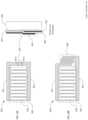
- FIG. 1includes a schematic plan view, two schematic cross-sectional views, and a detail view of a transversely-excited film bulk acoustic resonator (XBAR).
- XBARtransversely-excited film bulk acoustic resonator
- FIG. 2 Ais an equivalent circuit model of an acoustic resonator.
- FIG. 2 Bis a graph of the magnitude of admittance of an ideal acoustic resonator.
- FIG. 2 Cis a circuit symbol for an acoustic resonator.
- FIG. 3is a schematic block diagram of a band-pass filter using acoustic resonators.
- FIG. 4is a chart showing the magnitude of admittance of acoustic resonators relative to a target communications band.
- FIG. 5is a schematic block diagram of another band-pass filter using acoustic resonators.
- FIG. 6is chart showing the magnitude of admittance of series resonator subcircuits relative to a target communications band.
- FIG. 7is chart showing the magnitude of admittance of shunt resonator subcircuits relative to a target communications band.
- FIG. 8 Ais a schematic plan view and a cross-sectional detail view of an XBAR and a metal-insulator-metal (MIM) capacitor connected in parallel.
- MIMmetal-insulator-metal
- FIG. 8 Bis a schematic plan view of an XBAR and an interdigitated capacitor connected in parallel.
- FIG. 1shows a simplified schematic top view and orthogonal cross-sectional views of an XBAR 100 .
- XBAR-type resonatorssuch as the XBAR 100 may be used in a variety of RF filters including band-reject filters, band-pass filters, duplexers, and multiplexers.
- the XBAR 100is made up of a thin film conductor pattern formed on a surface of a piezoelectric plate 110 having parallel front and back surfaces 112 , 114 , respectively.
- the piezoelectric plateis a thin single-crystal layer of a piezoelectric material such as lithium niobate, lithium tantalate, lanthanum gallium silicate, gallium nitride, or aluminum nitride.
- the piezoelectric plateis cut such that the orientation of the X, Y, and Z crystalline axes with respect to the front and back surfaces is known and consistent.
- the piezoelectric platemay be Z-cut, which is to say the Z axis is normal to the front and back surfaces 112 , 114 .
- the piezoelectric platemay be rotated Z-cut or rotated YX-cut.
- XBARsmay be fabricated on piezoelectric plates with other crystallographic orientations.
- the back surface 114 of the piezoelectric plate 110is attached to a surface of a substrate 120 except for a portion of the piezoelectric plate 110 that forms a diaphragm 115 spanning a cavity 140 formed in the substrate.
- the portion of the piezoelectric plate that spans the cavityis referred to herein as the “diaphragm” 115 due to its physical resemblance to the diaphragm of a microphone.
- the diaphragm 115is contiguous with the rest of the piezoelectric plate 110 around all of a perimeter 145 of the cavity 140 .
- “contiguous”means “continuously connected without any intervening item”.
- the diaphragm 115may be contiguous with the piezoelectric plate around at least 50% of the perimeter 145 of the cavity 140 .
- the substrate 120provides mechanical support to the piezoelectric plate 110 .
- the substrate 120may be, for example, silicon, sapphire, quartz, or some other material or combination of materials.
- the back surface 114 of the piezoelectric plate 110may be attached to the substrate 120 using a wafer bonding process. Alternatively, the piezoelectric plate 110 may be grown on the substrate 120 or attached to the substrate in some other manner.
- the piezoelectric plate 110may be attached directly to the substrate or may be attached to the substrate 120 via one or more intermediate material layers (not shown in FIG. 1 ).
- the cavity 140has its conventional meaning of “an empty space within a solid body.”
- the cavity 140may be a hole completely through the substrate 120 (as shown in Section A-A and Section B-B) or a recess in the substrate 120 under the diaphragm 115 .
- the cavity 140may be formed, for example, by selective etching of the substrate 120 before or after the piezoelectric plate 110 and the substrate 120 are attached.
- the first and second busbars 132 , 134serve as the terminals of the XBAR 100 .
- a radio frequency or microwave signal applied between the two busbars 132 , 134 of the IDT 130excites a primary acoustic mode within the piezoelectric plate 110 .
- the primary acoustic modeis a bulk shear mode where acoustic energy propagates along a direction substantially orthogonal to the surface of the piezoelectric plate 110 , which is also normal, or transverse, to the direction of the electric field created by the IDT fingers.
- the XBARis considered a transversely-excited film bulk wave resonator.
- a thickness of the front side dielectric layer 150is typically less than about one-third of the thickness tp of the piezoelectric plate 110 .
- the front-side dielectric layer 150may be formed of multiple layers of two or more materials.
- a back-side dielectric layer(not shown) may be formed on the back side of the piezoelectric plate 110 .
- the IDT fingers 138 a , 138 bmay be one or more layers of aluminum, an aluminum alloy, copper, a copper alloy, beryllium, gold, tungsten, molybdenum, chromium, titanium or some other conductive material.
- the IDT fingersare considered to be “substantially aluminum” if they are formed from aluminum or an alloy comprising at least 50% aluminum.
- the IDT fingersare considered to be “substantially copper” if they are formed from copper or an alloy comprising at least 50% copper.
- Thin (relative to the total thickness of the conductors) layers of metals such as chromium or titaniummay be formed under and/or over and/or as layers within the fingers to improve adhesion between the fingers and the piezoelectric plate 110 and/or to passivate or encapsulate the fingers and/or to improve power handling.
- the busbars ( 132 , 134 in FIG. 1 ) of the IDTmay be made of the same or different materials as the fingers.
- Dimension pis the center-to-center spacing or “pitch” of the IDT fingers, which may be referred to as the pitch of the IDT and/or the pitch of the XBAR.
- Dimension mis the width or “mark” of the IDT fingers.
- the geometry of the IDT of an XBARdiffers substantially from the IDTs used in surface acoustic wave (SAW) resonators.
- SAWsurface acoustic wave
- the pitch of the IDTis one-half of the acoustic wavelength at the resonance frequency.
- the mark-to-pitch ratio of a SAW resonator IDTis typically close to 0.5 (i.e. the mark or finger width is about one-fourth of the acoustic wavelength at resonance).
- the pitch p of the IDTmay be 2 to 20 times the width m of the fingers.
- the pitch pis typically 3.3 to 5 times the width m of the fingers.
- the pitch p of the IDTmay be 2 to 20 times the thickness of the piezoelectric plate 210 .
- the pitch p of the IDTis typically 5 to 12.5 times the thickness of the piezoelectric plate 210 .
- the width m of the IDT fingers in an XBARis not constrained to be near one-fourth of the acoustic wavelength at resonance.
- the width of XBAR IDT fingersmay be 500 nm or greater, such that the IDT can be readily fabricated using optical lithography.
- the thickness of the IDT fingers 138 a , 138 bmay be from 100 nm to about equal to the width m.
- the thickness of the busbars ( 132 , 134 ) of the IDTmay be the same as, or greater than, the thickness of the IDT fingers.
- An XBAR based on shear acoustic wave resonancescan achieve better performance than current state-of-the art surface acoustic wave (SAW), film-bulk-acoustic-resonators (FBAR), and solidly-mounted-resonator bulk-acoustic-wave (SMR BAW) devices.
- SAWsurface acoustic wave
- FBARfilm-bulk-acoustic-resonators
- SMR BAWsolidly-mounted-resonator bulk-acoustic-wave
- the piezoelectric coupling for shear wave XBAR resonancescan be high (>20%) compared to other acoustic resonators.
- High piezoelectric couplingenables the design and implementation of microwave and millimeter-wave filters of various types with appreciable bandwidth.
- the basic behavior of acoustic resonators, including XBARs,is commonly described using the Butterworth Van Dyke (BVD) circuit model as shown in FIG. 2 A .
- the BVD circuit modelconsists of a motional arm and a static arm.
- the motional armincludes a motional inductance L m , a motional capacitance C m , and a resistance R m .
- the static armincludes a static capacitance C 0 and a resistance R 0 .
- the dashed linesshow an additional capacitor C 1 connected in parallel with the acoustic resonator.
- the capacitor C 1is not part of the acoustic resonator but may be present in some applications, as will be discussed subsequently.
- BVD modeldoes not fully describe the behavior of an acoustic resonator, it does a good job of modeling the two primary resonances that are used to design band-pass filters, duplexers, and multiplexers (multiplexers are filters with more than 2 input or output ports with multiple passbands).
- the first primary resonance of the BVD modelis the motional resonance caused by the series combination of the motional inductance L m and the motional capacitance C m .
- the second primary resonance of the BVD modelis the anti-resonance caused by the combination of the motional inductance L m , the motional capacitance C m , and the static capacitance C 0 .
- the frequency F r of the motional resonanceis given by
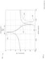
- FIG. 2 Bis a graph 200 of the performance of a theoretical lossless acoustic resonator.
- the solid curve 210is a plot of the magnitude of admittance of the acoustic resonator as a function of frequency.
- the acoustic resonatorhas a resonance 212 at a resonance frequency where the admittance of the resonator approaches infinity.
- the resonanceis due to the series combination of the motional inductance L m and the motional capacitance C m in the BVD model of FIG. 2 A .
- the acoustic resonatoralso exhibits an anti-resonance 214 where the admittance of the resonator approaches zero.
- the anti-resonanceis caused by the combination of the motional inductance L m , the motional capacitance C m , and the static capacitance C 0 .
- the frequency F r of the resonanceis given by
- the lossless acoustic resonatorcan be considered a short circuit at the resonance frequency 212 and an open circuit at the anti-resonance frequency 214 .
- the resonance and anti-resonance frequencies in FIG. 2 Bare representative, and an acoustic resonator may be designed for other frequencies.
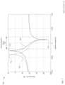
- Each of the resonators X 1 , X 2 , X 3 , X 4 , X 5 in the filter 300has resonance where the admittance of the resonator is very high and an anti-resonance where the admittance of the resonator is very low.
- the resonance and anti-resonanceoccur at a resonance frequency and an anti-resonance frequency, respectively, which may be the same or different for the various resonators in the filter 300 .
- each resonatorcan be considered a short-circuit at its resonance frequency and an open circuit at its anti-resonance frequency.
- the input-output transfer functionwill be near zero at the resonance frequencies of the shunt resonators and at the anti-resonance frequencies of the series resonators.
- shunt resonatorsprovide transmission zeros below the lower edge of the passband.
- the resonance frequencies of the shunt resonatorsare positioned below the lower edge of the filter's passband and the anti-resonance frequencies of the shunt resonators are within the passband.
- series resonatorsprovide transmission zeros above the passband. The resonance frequencies of the series resonators are within the passband and the anti-resonance frequencies of the series resonators are positioned above the upper edge of the passband.
- a front-side dielectric layer(also called a “frequency setting layer”), such as the layer 150 in FIG. 1 , may be formed on the shunt resonators to set the resonance frequencies of the shunt resonators lower relative to the resonance frequencies of the series resonators.
- the diaphragms of series resonatorsmay be thinner than the diaphragms of shunt resonators.
- the series resonators and the shunt resonatorsmay be fabricated on separate chips having different piezoelectric plate thicknesses.
- the two dot-dot-dash lines 412 , 414represent the lower and upper band edges, respectively, of a communications band 410 with a fractional bandwidth of 12.5%.
- Fractional bandwidthis defined herein as the difference between the frequencies of the upper and lower band edges divided by the center frequency.
- An example of a communications band with a fractional bandwidth about 12.5%is 5G NR band n79, which extends from 4400 MHz to 5000 MHz (fractional bandwidth ⁇ 12.8%).
- the interdigitated capacitor 880includes a plurality of interleaved fingers extending perpendicular to the interleaved fingers of the IDT 830 .
- a pitch of the interleaved capacitor fingersmay be less than the pitch of the IDT fingers and the mark/pitch ratio of the interleaved capacitor fingers may be about 50%.
- “plurality”means two or more. As used herein, a “set” of items may include one or more of such items.
- the terms “comprising”, “including”, “carrying”, “having”, “containing”, “involving”, and the likeare to be understood to be open-ended, i.e., to mean including but not limited to. Only the transitional phrases “consisting of” and “consisting essentially of”, respectively, are closed or semi-closed transitional phrases with respect to claims.
Landscapes
- Physics & Mathematics (AREA)
- Acoustics & Sound (AREA)
- Chemical & Material Sciences (AREA)
- Crystallography & Structural Chemistry (AREA)
- Piezo-Electric Or Mechanical Vibrators, Or Delay Or Filter Circuits (AREA)
Abstract
Description
where γ=C0/Cmis dependent on the resonator structure and the type and the orientation of the crystalline axes of the piezoelectric material.
The frequency Faof the anti-resonance is given by
Claims (15)
Priority Applications (1)
| Application Number | Priority Date | Filing Date | Title |
|---|---|---|---|
| US17/407,186US12308826B2 (en) | 2021-02-03 | 2021-08-20 | Bandpass filters using transversely-excited film bulk acoustic resonators |
Applications Claiming Priority (2)
| Application Number | Priority Date | Filing Date | Title |
|---|---|---|---|
| US202163144978P | 2021-02-03 | 2021-02-03 | |
| US17/407,186US12308826B2 (en) | 2021-02-03 | 2021-08-20 | Bandpass filters using transversely-excited film bulk acoustic resonators |
Publications (2)
| Publication Number | Publication Date |
|---|---|
| US20220247382A1 US20220247382A1 (en) | 2022-08-04 |
| US12308826B2true US12308826B2 (en) | 2025-05-20 |
Family
ID=82612825
Family Applications (1)
| Application Number | Title | Priority Date | Filing Date |
|---|---|---|---|
| US17/407,186Active2042-07-16US12308826B2 (en) | 2021-02-03 | 2021-08-20 | Bandpass filters using transversely-excited film bulk acoustic resonators |
Country Status (1)
| Country | Link |
|---|---|
| US (1) | US12308826B2 (en) |
Families Citing this family (2)
| Publication number | Priority date | Publication date | Assignee | Title |
|---|---|---|---|---|
| US12413207B2 (en)* | 2021-09-28 | 2025-09-09 | Skyworks Global Pte. Ltd. | Passband filter combining resonators of a first type and resonators of a second type |
| KR20240041489A (en)* | 2022-09-23 | 2024-04-01 | (주)와이솔 | Surface accoustic wave filter with improved attenuation |
Citations (122)
| Publication number | Priority date | Publication date | Assignee | Title |
|---|---|---|---|---|
| US5446330A (en) | 1993-03-15 | 1995-08-29 | Matsushita Electric Industrial Co., Ltd. | Surface acoustic wave device having a lamination structure |
| US5552655A (en) | 1994-05-04 | 1996-09-03 | Trw Inc. | Low frequency mechanical resonator |
| US5726610A (en) | 1995-06-19 | 1998-03-10 | Motorola Inc. | Saw filter device for radio tranceiver utilizing different coupling coefficient ratios |
| US5853601A (en) | 1997-04-03 | 1998-12-29 | Northrop Grumman Corporation | Top-via etch technique for forming dielectric membranes |
| US6377140B1 (en) | 1999-07-09 | 2002-04-23 | Oki Electric Industry Co., Ltd. | Saw resonator filter with bridged-T configuration |
| US20020079986A1 (en) | 2000-12-21 | 2002-06-27 | Ruby Richard C. | Bulk acoustic resonator perimeter reflection system |
| US20020158714A1 (en) | 2001-04-27 | 2002-10-31 | Nokia Corporation | Method and system for wafer-level tuning of bulk acoustic wave resonators and filters by reducing thickness non-uniformity |
| US20020189062A1 (en) | 2001-06-15 | 2002-12-19 | Asia Pacific Microsystems, Inc. | Manufacturing method for a high quality film bulk acoustic wave device |
| US6516503B1 (en) | 1999-05-26 | 2003-02-11 | Murata Manufacturing Co., Ltd. | Method of making surface acoustic wave device |
| US6540827B1 (en) | 1998-02-17 | 2003-04-01 | Trustees Of Columbia University In The City Of New York | Slicing of single-crystal films using ion implantation |
| US20030080831A1 (en) | 2001-10-25 | 2003-05-01 | Naumenko Natalya F. | Surface acoustic wave devices using optimized cuts of lithium niobate (LiNbO3) |
| US20030199105A1 (en) | 2002-04-22 | 2003-10-23 | Kub Francis J. | Method for making piezoelectric resonator and surface acoustic wave device using hydrogen implant layer splitting |
| US6707229B1 (en) | 1999-06-03 | 2004-03-16 | Tele Filter Zweigniederlassung Der Dover Germany Gmbh | Surface acoustic wave filter |
| US20040100164A1 (en) | 2002-11-26 | 2004-05-27 | Murata Manufacturing Co., Ltd. | Manufacturing method of electronic device |
| US20040261250A1 (en) | 2000-09-06 | 2004-12-30 | Murata Manufacturing Co., Ltd. | Method for adjusting a frequency characteristic of an edge reflection type surface acoustic wave device and method for producing an- edge reflection type surface acoustic wave device |
| US20050185026A1 (en) | 2004-01-26 | 2005-08-25 | Motohisa Noguchi | Piezoelectric element, piezoelectric actuator, ink jet recording head, ink jet printer, surface acoustic wave element, frequency filter, oscillator, electronic circuit, thin film piezoelectric resonator, and electronic apparatus |
| US20050218488A1 (en) | 2004-03-31 | 2005-10-06 | Mie Matsuo | Electronic component having micro-electrical mechanical system |
| US20050264136A1 (en) | 2004-05-31 | 2005-12-01 | Jun Tsutsumi | Surface acoustic wave device |
| US20050280476A1 (en)* | 2004-06-15 | 2005-12-22 | Kabushiki Kaisha Toshiba | Filter control apparatus and filter system |
| US20060179642A1 (en) | 2005-02-03 | 2006-08-17 | Kabushiki Kaisha Toshiba | Method for manufacturing a film bulk acoustic resonator |
| US7135940B2 (en)* | 2004-01-30 | 2006-11-14 | Kabushiki Kaisha Toshiba | Tunable filter and portable telephone |
| US20070182510A1 (en) | 2006-02-06 | 2007-08-09 | Samsung Electronics Co., Ltd. | Multi-band filter module and method of fabricating the same |
| US20070188047A1 (en) | 2006-02-16 | 2007-08-16 | Seiko Epson Corporation | Lamb wave type frequency device and method thereof |
| US20070194863A1 (en) | 2006-02-17 | 2007-08-23 | Kabushiki Kaisha Toshiba | Film bulk acoustic resonator and method of manufacturing same |
| US20070267942A1 (en) | 2006-05-19 | 2007-11-22 | Hisanori Matsumoto | Piezoelectric film resonator, radio-frequency filter using them, and radio-frequency module using them |
| US7345400B2 (en) | 2003-01-27 | 2008-03-18 | Murata Manufacturing Co., Ltd. | Surface acoustic wave device |
| US20080246559A1 (en) | 2007-01-19 | 2008-10-09 | Farrokh Ayazi | Lithographically-defined multi-standard multi-frequency high-Q tunable micromechanical resonators |
| US7463118B2 (en) | 2006-06-09 | 2008-12-09 | Texas Instruments Incorporated | Piezoelectric resonator with an efficient all-dielectric Bragg reflector |
| US7535152B2 (en) | 2005-10-19 | 2009-05-19 | Murata Manufacturing Co., Ltd. | Lamb wave device |
| US7684109B2 (en) | 2007-02-28 | 2010-03-23 | Maxim Integrated Products, Inc. | Bragg mirror optimized for shear waves |
| US7688161B2 (en)* | 2006-10-25 | 2010-03-30 | Fujitsu Media Devices Limited | Acoustic wave device and filter using the same |
| US20100123367A1 (en) | 2008-11-19 | 2010-05-20 | Ngk Insulators, Ltd. | Lamb wave device |
| US7868519B2 (en) | 2007-09-06 | 2011-01-11 | Murata Manufacturing Co., Ltd. | Piezoelectric resonator including an acoustic reflector portion |
| US20110018389A1 (en) | 2008-01-30 | 2011-01-27 | Kyocera Corporation | Acoustic Wave Device and Method for Production of Same |
| US20110018654A1 (en) | 2009-07-27 | 2011-01-27 | Avago Technologies Wireless Ip (Singapore) Pte. Ltd. | Resonator filter with multiple cross-couplings |
| US7941103B2 (en) | 2005-11-15 | 2011-05-10 | Taiyo Yuden Co., Ltd. | Duplexer |
| US20110109196A1 (en) | 2008-07-11 | 2011-05-12 | Goto Rei | Plate wave element and electronic equipment using same |
| US20110278993A1 (en) | 2010-05-17 | 2011-11-17 | Murata Manufacturing Co., Ltd. | Method for manufacturing composite piezoelectric substrate and piezoelectric device |
| US8278802B1 (en) | 2008-04-24 | 2012-10-02 | Rf Micro Devices, Inc. | Planarized sacrificial layer for MEMS fabrication |
| US8294330B1 (en) | 2009-03-31 | 2012-10-23 | Triquint Semiconductor, Inc. | High coupling, low loss saw filter and associated method |
| US20120286900A1 (en) | 2010-01-28 | 2012-11-15 | Murata Manufacturing Co., Ltd. | Tunable filter |
| US8344815B2 (en) | 2008-10-24 | 2013-01-01 | Seiko Epson Corporation | Surface acoustic wave resonator, surface acoustic wave oscillator, and surface acoustic wave module unit |
| US20130234805A1 (en) | 2012-03-07 | 2013-09-12 | Taiyo Yuden Co., Ltd. | Resonator, frequency filter, duplexer, electronic device, and method of manufacturing resonator |
| US20130271238A1 (en) | 2012-04-13 | 2013-10-17 | Taiyo Yuden Co., Ltd. | Filter device, manufacturing method for filter device, and duplexer |
| US20130278609A1 (en) | 2012-04-19 | 2013-10-24 | Qualcomm Mems Technologies, Inc. | Isotropically-etched cavities for evanescent-mode electromagnetic-wave cavity resonators |
| US20130321100A1 (en) | 2012-06-05 | 2013-12-05 | Avago Technologies Wireless Ip (Singapore) Pte. Ltd. | Laterally-coupled acoustic resonators |
| US20140130319A1 (en) | 2010-09-28 | 2014-05-15 | Murata Manufacturing Co., Ltd. | Method for manufacturing piezoelectric device |
| US20140145556A1 (en) | 2011-08-08 | 2014-05-29 | Murata Manufacturing Co., Ltd. | Elastic wave device |
| US20140152145A1 (en) | 2010-11-30 | 2014-06-05 | Murata Manufacturing Co., Ltd. | Elastic wave device and manufacturing method for same |
| US20140151151A1 (en) | 2010-10-15 | 2014-06-05 | Commissariat A L'energie Atomique Et Aux Energies Alternatives | Heterogenous acoustic structure formed from a homogeneous material |
| US20140173862A1 (en) | 2007-12-25 | 2014-06-26 | Murata Manufacturing Co., Ltd. | Method for manufacturing composite piezoelectric substrate |
| US20140225684A1 (en) | 2011-10-24 | 2014-08-14 | Murata Manufacturing Co., Ltd. | Surface acoustic wave device |
| US8816567B2 (en) | 2011-07-19 | 2014-08-26 | Qualcomm Mems Technologies, Inc. | Piezoelectric laterally vibrating resonator structure geometries for spurious frequency suppression |
| US8829766B2 (en) | 2008-08-01 | 2014-09-09 | Epcos Ag | Piezoelectric resonator operating in thickness shear mode |
| US8932686B2 (en) | 2008-10-31 | 2015-01-13 | Murata Manufacturing Co., Ltd. | Method for producing piezoelectric composite substrate |
| US20150042417A1 (en) | 2013-08-06 | 2015-02-12 | Murata Manufacturing Co., Ltd. | High-frequency module |
| US9130145B2 (en) | 2012-03-29 | 2015-09-08 | Vectron International Gmbh | Surface acoustic wave component |
| US20150319537A1 (en) | 2012-12-12 | 2015-11-05 | Epcos Ag | Electroacoustic Components and Methods Thereof |
| US20150333730A1 (en) | 2010-04-23 | 2015-11-19 | Teknologian Tutkimuskeskus Vtt Oy | Wide-band acoustically coupled thin-film BAW filter |
| US9219466B2 (en) | 2011-11-11 | 2015-12-22 | Teknologian Tutkimuskeskus Vtt Oy | Laterally coupled bulk acoustic wave filter with improved passband characteristics |
| US20160028367A1 (en) | 2014-07-25 | 2016-01-28 | Akoustis, Inc. | Single crystal acoustic resonator and bulk acoustic wave filter |
| WO2016017104A1 (en) | 2014-07-31 | 2016-02-04 | Skyworks Panasonic Filter Solutions Japan Co., Ltd. | Acoustic wave filters and duplexers using same |
| US9276557B1 (en) | 2013-07-01 | 2016-03-01 | Sandia Corporation | Programmable electroacoustic filter apparatus and method for its manufacture |
| US9369105B1 (en) | 2007-08-31 | 2016-06-14 | Rf Micro Devices, Inc. | Method for manufacturing a vibrating MEMS circuit |
| US20160182009A1 (en) | 2014-12-17 | 2016-06-23 | Rf Micro Devices, Inc. | Plate wave devices with wave confinement structures and fabrication methods |
| US9425765B2 (en) | 2013-04-22 | 2016-08-23 | Northeastern University | Nano- and micro-electromechanical resonators |
| US9525398B1 (en) | 2014-05-27 | 2016-12-20 | Sandia Corporation | Single crystal micromechanical resonator and fabrication methods thereof |
| US20170063332A1 (en) | 2015-08-25 | 2017-03-02 | Avago Technologies General Ip (Singapore) Pte. Ltd. | Surface acoustic wave (saw) resonator having trap-rich region |
| US9607119B1 (en)* | 2015-11-13 | 2017-03-28 | Resonant Inc. | Simulating effects of temperature on acoustic microwave filters |
| US9640750B2 (en) | 2011-03-25 | 2017-05-02 | Skyworks Filter Solutions Japan Co., Ltd. | Acoustic wave device with suppressed higher order transverse modes |
| US20170179225A1 (en) | 2011-05-25 | 2017-06-22 | Semiconductor Components Industries, Llc | Semiconductor device having a super junction structure and method of manufacturing the same |
| US20170179928A1 (en) | 2015-11-13 | 2017-06-22 | Resonant Inc. | Acoustic wave filter with enhanced rejection |
| US20170214381A1 (en) | 2016-01-22 | 2017-07-27 | Rf Micro Devices, Inc. | Guided wave devices with selectively thinned piezoelectric layers |
| US20170214387A1 (en) | 2016-01-26 | 2017-07-27 | Avago Technologies General Ip (Singapore) Pte. Ltd. | Bulk acoustic wave resonator with piezoelectric layer comprising lithium niobate or lithium tantalate |
| US20170222617A1 (en) | 2014-10-16 | 2017-08-03 | Murata Manufacturing Co., Ltd. | High-frequency module |
| US20170222622A1 (en) | 2016-01-28 | 2017-08-03 | Triquint Semiconductor, Inc. | Surface acoustic wave device having a piezoelectric layer on a quartz substrate and methods of manufacturing thereof |
| US9762202B2 (en) | 2008-12-17 | 2017-09-12 | Analog Devices, Inc. | Method of manufacturing a mechanical resonating structure |
| US9780759B2 (en) | 2010-12-24 | 2017-10-03 | Murata Manufacturing Co., Ltd. | Elastic wave device and method for manufacturing the same |
| US9837984B2 (en) | 2014-12-24 | 2017-12-05 | Qorvo Us, Inc. | RF ladder filter with simplified acoustic RF resonator parallel capacitance compensation |
| US20170370791A1 (en) | 2016-06-28 | 2017-12-28 | Taiyo Yuden Co., Ltd. | Method of fabricating acoustic wave device and acoustic wave device |
| US20180005950A1 (en) | 2016-06-29 | 2018-01-04 | Murata Manufacturing Co., Ltd. | Electronic component device, method of mounting electronic component device on circuit board, and mounting structure of electronic component device on circuit board |
| WO2018003273A1 (en) | 2016-06-28 | 2018-01-04 | 株式会社村田製作所 | Multiplexer, high-frequency front end circuit, and communication device |
| US20180026603A1 (en) | 2015-05-22 | 2018-01-25 | Murata Manufacturing Co., Ltd. | Electronic component |
| US20180033952A1 (en) | 2016-07-28 | 2018-02-01 | Taiyo Yuden Co., Ltd. | Electronic device and method of fabricating the same |
| US20180062617A1 (en) | 2016-08-25 | 2018-03-01 | Qualcomm Incorporated | Single-chip multi-frequency film bulk acoustic-wave resonators |
| US20180062615A1 (en) | 2015-05-08 | 2018-03-01 | Murata Manufacturing Co., Ltd. | High frequency module |
| US20180123016A1 (en) | 2012-06-15 | 2018-05-03 | Carnegie Mellon University | Microelectronic structures with suspended lithium-based thin films |
| US20180191322A1 (en) | 2017-01-03 | 2018-07-05 | Win Semiconductors Corp. | Method for fabricating bulk acoustic wave resonator with mass adjustment structure |
| US10050601B2 (en)* | 2015-01-07 | 2018-08-14 | Murata Manufacturing Co., Ltd. | Elastic wave apparatus |
| US10079414B2 (en) | 2015-03-17 | 2018-09-18 | The United States Of America, As Represented By The Secretary Of The Navy | Switched multiplexer with flat group delay and channelized limiting |
| US10187039B2 (en) | 2016-06-07 | 2019-01-22 | Skyworks Filter Solutions Japan Co., Ltd. | Filter devices having reduced spurious emissions from lamb waves |
| US10200013B2 (en) | 2016-02-18 | 2019-02-05 | X-Celeprint Limited | Micro-transfer-printed acoustic wave filter device |
| US20190068164A1 (en) | 2016-03-11 | 2019-02-28 | Akoustis, Inc. | 5G BAND n79 ACOUSTIC WAVE RESONATOR RF FILTER CIRCUIT |
| US20190131953A1 (en) | 2017-10-31 | 2019-05-02 | The Board Of Trustees Of The University Of Illinois | Interdigital transducers on a piezoelectric thin-film for signal compression |
| US10284176B1 (en) | 2015-06-03 | 2019-05-07 | Qorvo Us, Inc. | Temperature compensated surface acoustic wave device and methods of manufacturing the same |
| US20190273480A1 (en) | 2018-03-02 | 2019-09-05 | Skyworks Solutions, Inc. | Lamb wave loop circuit for acoustic wave filter |
| US20190348966A1 (en) | 2018-05-10 | 2019-11-14 | Globalfoundries Singapore Pte. Ltd. | Acoustic wave filter formed on a v-groove topography and method for producing the same |
| US10491192B1 (en) | 2018-06-15 | 2019-11-26 | Resonant Inc. | Transversely-excited film bulk acoustic resonator |
| US20200036357A1 (en) | 2017-04-26 | 2020-01-30 | Murata Manufacturing Co., Ltd. | Acoustic wave device |
| US10601392B2 (en) | 2018-06-15 | 2020-03-24 | Resonant Inc. | Solidly-mounted transversely-excited film bulk acoustic resonator |
| US10637438B2 (en) | 2018-06-15 | 2020-04-28 | Resonant Inc. | Transversely-excited film bulk acoustic resonators for high power applications |
| US20200220522A1 (en)* | 2017-09-28 | 2020-07-09 | Murata Manufacturing Co., Ltd. | Filter device, multiplexer, radio frequency front-end circuit, and communication device |
| US20200235719A1 (en) | 2018-06-15 | 2020-07-23 | Resonant Inc. | Xbar resonators with non-rectangular diaphragms |
| US20200235720A1 (en)* | 2017-10-16 | 2020-07-23 | Murata Manufacturing Co., Ltd. | Acoustic wave filter, multiplexer, radio frequency front-end circuit, and communication device |
| US10756697B2 (en) | 2018-06-15 | 2020-08-25 | Resonant Inc. | Transversely-excited film bulk acoustic resonator |
| US10790802B2 (en) | 2018-06-15 | 2020-09-29 | Resonant Inc. | Transversely excited film bulk acoustic resonator using rotated Y-X cut lithium niobate |
| US10797675B2 (en) | 2018-06-15 | 2020-10-06 | Resonant Inc. | Transversely excited film bulk acoustic resonator using rotated z-cut lithium niobate |
| US10819309B1 (en) | 2019-04-05 | 2020-10-27 | Resonant Inc. | Transversely-excited film bulk acoustic resonator package and method |
| US10826462B2 (en) | 2018-06-15 | 2020-11-03 | Resonant Inc. | Transversely-excited film bulk acoustic resonators with molybdenum conductors |
| US10868510B2 (en) | 2018-06-15 | 2020-12-15 | Resonant Inc. | Transversely-excited film bulk acoustic resonator with half-lambda dielectric layer |
| US10868513B2 (en) | 2018-06-15 | 2020-12-15 | Resonant Inc. | Transversely-excited film bulk acoustic filters with symmetric layout |
| US10911023B2 (en) | 2018-06-15 | 2021-02-02 | Resonant Inc. | Transversely-excited film bulk acoustic resonator with etch-stop layer |
| US10911021B2 (en) | 2019-06-27 | 2021-02-02 | Resonant Inc. | Transversely-excited film bulk acoustic resonator with lateral etch stop |
| US10917072B2 (en) | 2019-06-24 | 2021-02-09 | Resonant Inc. | Split ladder acoustic wave filters |
| US10985728B2 (en) | 2018-06-15 | 2021-04-20 | Resonant Inc. | Transversely-excited film bulk acoustic resonator and filter with a uniform-thickness dielectric overlayer |
| US10992284B2 (en) | 2018-06-15 | 2021-04-27 | Resonant Inc. | Filter using transversely-excited film bulk acoustic resonators with multiple frequency setting layers |
| US10992283B2 (en) | 2018-06-15 | 2021-04-27 | Resonant Inc. | High power transversely-excited film bulk acoustic resonators on rotated Z-cut lithium niobate |
| US10992282B1 (en) | 2020-06-18 | 2021-04-27 | Resonant Inc. | Transversely-excited film bulk acoustic resonators with electrodes having a second layer of variable width |
| US10998877B2 (en) | 2018-06-15 | 2021-05-04 | Resonant Inc. | Film bulk acoustic resonator fabrication method with frequency trimming based on electric measurements prior to cavity etch |
| US11003971B2 (en) | 2017-11-07 | 2021-05-11 | Resonant Inc. | Ultra-wide-band saw sensor with hyperbolically frequency-modulated etched reflector |
| US20220158624A1 (en)* | 2020-11-13 | 2022-05-19 | Tai-Saw Technology Co., Ltd. | Acoustic-wave ladder filter having impedance element and diplexer based thereon |
| US11563423B2 (en)* | 2018-05-25 | 2023-01-24 | Skyworks Solutions, Inc. | Filter including acoustic wave resonator in parallel with circuit element |
- 2021
- 2021-08-20USUS17/407,186patent/US12308826B2/enactiveActive
Patent Citations (140)
| Publication number | Priority date | Publication date | Assignee | Title |
|---|---|---|---|---|
| US5446330A (en) | 1993-03-15 | 1995-08-29 | Matsushita Electric Industrial Co., Ltd. | Surface acoustic wave device having a lamination structure |
| US5552655A (en) | 1994-05-04 | 1996-09-03 | Trw Inc. | Low frequency mechanical resonator |
| US5726610A (en) | 1995-06-19 | 1998-03-10 | Motorola Inc. | Saw filter device for radio tranceiver utilizing different coupling coefficient ratios |
| US5853601A (en) | 1997-04-03 | 1998-12-29 | Northrop Grumman Corporation | Top-via etch technique for forming dielectric membranes |
| US6540827B1 (en) | 1998-02-17 | 2003-04-01 | Trustees Of Columbia University In The City Of New York | Slicing of single-crystal films using ion implantation |
| US6710514B2 (en) | 1999-05-26 | 2004-03-23 | Murata Manufacturing Co., Ltd. | Surface acoustic wave device |
| US6516503B1 (en) | 1999-05-26 | 2003-02-11 | Murata Manufacturing Co., Ltd. | Method of making surface acoustic wave device |
| US6707229B1 (en) | 1999-06-03 | 2004-03-16 | Tele Filter Zweigniederlassung Der Dover Germany Gmbh | Surface acoustic wave filter |
| US6377140B1 (en) | 1999-07-09 | 2002-04-23 | Oki Electric Industry Co., Ltd. | Saw resonator filter with bridged-T configuration |
| US20040261250A1 (en) | 2000-09-06 | 2004-12-30 | Murata Manufacturing Co., Ltd. | Method for adjusting a frequency characteristic of an edge reflection type surface acoustic wave device and method for producing an- edge reflection type surface acoustic wave device |
| US20020079986A1 (en) | 2000-12-21 | 2002-06-27 | Ruby Richard C. | Bulk acoustic resonator perimeter reflection system |
| US20020158714A1 (en) | 2001-04-27 | 2002-10-31 | Nokia Corporation | Method and system for wafer-level tuning of bulk acoustic wave resonators and filters by reducing thickness non-uniformity |
| US20020189062A1 (en) | 2001-06-15 | 2002-12-19 | Asia Pacific Microsystems, Inc. | Manufacturing method for a high quality film bulk acoustic wave device |
| US20030080831A1 (en) | 2001-10-25 | 2003-05-01 | Naumenko Natalya F. | Surface acoustic wave devices using optimized cuts of lithium niobate (LiNbO3) |
| US20030199105A1 (en) | 2002-04-22 | 2003-10-23 | Kub Francis J. | Method for making piezoelectric resonator and surface acoustic wave device using hydrogen implant layer splitting |
| US20040100164A1 (en) | 2002-11-26 | 2004-05-27 | Murata Manufacturing Co., Ltd. | Manufacturing method of electronic device |
| US7345400B2 (en) | 2003-01-27 | 2008-03-18 | Murata Manufacturing Co., Ltd. | Surface acoustic wave device |
| US20050185026A1 (en) | 2004-01-26 | 2005-08-25 | Motohisa Noguchi | Piezoelectric element, piezoelectric actuator, ink jet recording head, ink jet printer, surface acoustic wave element, frequency filter, oscillator, electronic circuit, thin film piezoelectric resonator, and electronic apparatus |
| US7135940B2 (en)* | 2004-01-30 | 2006-11-14 | Kabushiki Kaisha Toshiba | Tunable filter and portable telephone |
| US20050218488A1 (en) | 2004-03-31 | 2005-10-06 | Mie Matsuo | Electronic component having micro-electrical mechanical system |
| US20050264136A1 (en) | 2004-05-31 | 2005-12-01 | Jun Tsutsumi | Surface acoustic wave device |
| US20050280476A1 (en)* | 2004-06-15 | 2005-12-22 | Kabushiki Kaisha Toshiba | Filter control apparatus and filter system |
| US20060179642A1 (en) | 2005-02-03 | 2006-08-17 | Kabushiki Kaisha Toshiba | Method for manufacturing a film bulk acoustic resonator |
| US7535152B2 (en) | 2005-10-19 | 2009-05-19 | Murata Manufacturing Co., Ltd. | Lamb wave device |
| US7941103B2 (en) | 2005-11-15 | 2011-05-10 | Taiyo Yuden Co., Ltd. | Duplexer |
| US20070182510A1 (en) | 2006-02-06 | 2007-08-09 | Samsung Electronics Co., Ltd. | Multi-band filter module and method of fabricating the same |
| US7728483B2 (en) | 2006-02-16 | 2010-06-01 | Seiko Epson Corporation | Lamb wave type frequency device and method thereof |
| US20070188047A1 (en) | 2006-02-16 | 2007-08-16 | Seiko Epson Corporation | Lamb wave type frequency device and method thereof |
| US20100064492A1 (en) | 2006-02-16 | 2010-03-18 | Seiko Epson Corporation | Lamb wave type frequency device and method thereof |
| US20070194863A1 (en) | 2006-02-17 | 2007-08-23 | Kabushiki Kaisha Toshiba | Film bulk acoustic resonator and method of manufacturing same |
| US20070267942A1 (en) | 2006-05-19 | 2007-11-22 | Hisanori Matsumoto | Piezoelectric film resonator, radio-frequency filter using them, and radio-frequency module using them |
| US7463118B2 (en) | 2006-06-09 | 2008-12-09 | Texas Instruments Incorporated | Piezoelectric resonator with an efficient all-dielectric Bragg reflector |
| US7688161B2 (en)* | 2006-10-25 | 2010-03-30 | Fujitsu Media Devices Limited | Acoustic wave device and filter using the same |
| US20080246559A1 (en) | 2007-01-19 | 2008-10-09 | Farrokh Ayazi | Lithographically-defined multi-standard multi-frequency high-Q tunable micromechanical resonators |
| US7684109B2 (en) | 2007-02-28 | 2010-03-23 | Maxim Integrated Products, Inc. | Bragg mirror optimized for shear waves |
| US9369105B1 (en) | 2007-08-31 | 2016-06-14 | Rf Micro Devices, Inc. | Method for manufacturing a vibrating MEMS circuit |
| US7868519B2 (en) | 2007-09-06 | 2011-01-11 | Murata Manufacturing Co., Ltd. | Piezoelectric resonator including an acoustic reflector portion |
| US20140173862A1 (en) | 2007-12-25 | 2014-06-26 | Murata Manufacturing Co., Ltd. | Method for manufacturing composite piezoelectric substrate |
| US20110018389A1 (en) | 2008-01-30 | 2011-01-27 | Kyocera Corporation | Acoustic Wave Device and Method for Production of Same |
| US8278802B1 (en) | 2008-04-24 | 2012-10-02 | Rf Micro Devices, Inc. | Planarized sacrificial layer for MEMS fabrication |
| US20110109196A1 (en) | 2008-07-11 | 2011-05-12 | Goto Rei | Plate wave element and electronic equipment using same |
| US8829766B2 (en) | 2008-08-01 | 2014-09-09 | Epcos Ag | Piezoelectric resonator operating in thickness shear mode |
| US8344815B2 (en) | 2008-10-24 | 2013-01-01 | Seiko Epson Corporation | Surface acoustic wave resonator, surface acoustic wave oscillator, and surface acoustic wave module unit |
| US8932686B2 (en) | 2008-10-31 | 2015-01-13 | Murata Manufacturing Co., Ltd. | Method for producing piezoelectric composite substrate |
| US20100123367A1 (en) | 2008-11-19 | 2010-05-20 | Ngk Insulators, Ltd. | Lamb wave device |
| US7965015B2 (en) | 2008-11-19 | 2011-06-21 | Ngk Insulators, Ltd. | Lamb wave device |
| US9762202B2 (en) | 2008-12-17 | 2017-09-12 | Analog Devices, Inc. | Method of manufacturing a mechanical resonating structure |
| US8294330B1 (en) | 2009-03-31 | 2012-10-23 | Triquint Semiconductor, Inc. | High coupling, low loss saw filter and associated method |
| US20110018654A1 (en) | 2009-07-27 | 2011-01-27 | Avago Technologies Wireless Ip (Singapore) Pte. Ltd. | Resonator filter with multiple cross-couplings |
| US20120286900A1 (en) | 2010-01-28 | 2012-11-15 | Murata Manufacturing Co., Ltd. | Tunable filter |
| US20150333730A1 (en) | 2010-04-23 | 2015-11-19 | Teknologian Tutkimuskeskus Vtt Oy | Wide-band acoustically coupled thin-film BAW filter |
| US20110278993A1 (en) | 2010-05-17 | 2011-11-17 | Murata Manufacturing Co., Ltd. | Method for manufacturing composite piezoelectric substrate and piezoelectric device |
| US20140130319A1 (en) | 2010-09-28 | 2014-05-15 | Murata Manufacturing Co., Ltd. | Method for manufacturing piezoelectric device |
| US20140151151A1 (en) | 2010-10-15 | 2014-06-05 | Commissariat A L'energie Atomique Et Aux Energies Alternatives | Heterogenous acoustic structure formed from a homogeneous material |
| US9748923B2 (en) | 2010-11-30 | 2017-08-29 | Murata Manufacturing Co., Ltd. | Elastic wave device and manufacturing method for same |
| US20140152145A1 (en) | 2010-11-30 | 2014-06-05 | Murata Manufacturing Co., Ltd. | Elastic wave device and manufacturing method for same |
| US9780759B2 (en) | 2010-12-24 | 2017-10-03 | Murata Manufacturing Co., Ltd. | Elastic wave device and method for manufacturing the same |
| US9640750B2 (en) | 2011-03-25 | 2017-05-02 | Skyworks Filter Solutions Japan Co., Ltd. | Acoustic wave device with suppressed higher order transverse modes |
| US20170179225A1 (en) | 2011-05-25 | 2017-06-22 | Semiconductor Components Industries, Llc | Semiconductor device having a super junction structure and method of manufacturing the same |
| US8816567B2 (en) | 2011-07-19 | 2014-08-26 | Qualcomm Mems Technologies, Inc. | Piezoelectric laterally vibrating resonator structure geometries for spurious frequency suppression |
| US20140145556A1 (en) | 2011-08-08 | 2014-05-29 | Murata Manufacturing Co., Ltd. | Elastic wave device |
| US20140225684A1 (en) | 2011-10-24 | 2014-08-14 | Murata Manufacturing Co., Ltd. | Surface acoustic wave device |
| US9219466B2 (en) | 2011-11-11 | 2015-12-22 | Teknologian Tutkimuskeskus Vtt Oy | Laterally coupled bulk acoustic wave filter with improved passband characteristics |
| US9112134B2 (en) | 2012-03-07 | 2015-08-18 | Taiyo Yuden Co., Ltd. | Resonator, frequency filter, duplexer, electronic device, and method of manufacturing resonator |
| US20130234805A1 (en) | 2012-03-07 | 2013-09-12 | Taiyo Yuden Co., Ltd. | Resonator, frequency filter, duplexer, electronic device, and method of manufacturing resonator |
| US9130145B2 (en) | 2012-03-29 | 2015-09-08 | Vectron International Gmbh | Surface acoustic wave component |
| US20130271238A1 (en) | 2012-04-13 | 2013-10-17 | Taiyo Yuden Co., Ltd. | Filter device, manufacturing method for filter device, and duplexer |
| US20130278609A1 (en) | 2012-04-19 | 2013-10-24 | Qualcomm Mems Technologies, Inc. | Isotropically-etched cavities for evanescent-mode electromagnetic-wave cavity resonators |
| US9093979B2 (en) | 2012-06-05 | 2015-07-28 | Avago Technologies General Ip (Singapore) Pte. Ltd. | Laterally-coupled acoustic resonators |
| US20130321100A1 (en) | 2012-06-05 | 2013-12-05 | Avago Technologies Wireless Ip (Singapore) Pte. Ltd. | Laterally-coupled acoustic resonators |
| US20180123016A1 (en) | 2012-06-15 | 2018-05-03 | Carnegie Mellon University | Microelectronic structures with suspended lithium-based thin films |
| US20150319537A1 (en) | 2012-12-12 | 2015-11-05 | Epcos Ag | Electroacoustic Components and Methods Thereof |
| US9425765B2 (en) | 2013-04-22 | 2016-08-23 | Northeastern University | Nano- and micro-electromechanical resonators |
| US9276557B1 (en) | 2013-07-01 | 2016-03-01 | Sandia Corporation | Programmable electroacoustic filter apparatus and method for its manufacture |
| US20150042417A1 (en) | 2013-08-06 | 2015-02-12 | Murata Manufacturing Co., Ltd. | High-frequency module |
| US9525398B1 (en) | 2014-05-27 | 2016-12-20 | Sandia Corporation | Single crystal micromechanical resonator and fabrication methods thereof |
| US20160028367A1 (en) | 2014-07-25 | 2016-01-28 | Akoustis, Inc. | Single crystal acoustic resonator and bulk acoustic wave filter |
| WO2016017104A1 (en) | 2014-07-31 | 2016-02-04 | Skyworks Panasonic Filter Solutions Japan Co., Ltd. | Acoustic wave filters and duplexers using same |
| US20170222617A1 (en) | 2014-10-16 | 2017-08-03 | Murata Manufacturing Co., Ltd. | High-frequency module |
| US20160182009A1 (en) | 2014-12-17 | 2016-06-23 | Rf Micro Devices, Inc. | Plate wave devices with wave confinement structures and fabrication methods |
| US9837984B2 (en) | 2014-12-24 | 2017-12-05 | Qorvo Us, Inc. | RF ladder filter with simplified acoustic RF resonator parallel capacitance compensation |
| US10050601B2 (en)* | 2015-01-07 | 2018-08-14 | Murata Manufacturing Co., Ltd. | Elastic wave apparatus |
| US10079414B2 (en) | 2015-03-17 | 2018-09-18 | The United States Of America, As Represented By The Secretary Of The Navy | Switched multiplexer with flat group delay and channelized limiting |
| US20180062615A1 (en) | 2015-05-08 | 2018-03-01 | Murata Manufacturing Co., Ltd. | High frequency module |
| US20180026603A1 (en) | 2015-05-22 | 2018-01-25 | Murata Manufacturing Co., Ltd. | Electronic component |
| US10284176B1 (en) | 2015-06-03 | 2019-05-07 | Qorvo Us, Inc. | Temperature compensated surface acoustic wave device and methods of manufacturing the same |
| US20170063332A1 (en) | 2015-08-25 | 2017-03-02 | Avago Technologies General Ip (Singapore) Pte. Ltd. | Surface acoustic wave (saw) resonator having trap-rich region |
| US10305447B2 (en)* | 2015-11-13 | 2019-05-28 | Resonant Inc. | Acoustic wave filter with enhanced rejection |
| US20170179928A1 (en) | 2015-11-13 | 2017-06-22 | Resonant Inc. | Acoustic wave filter with enhanced rejection |
| US9607119B1 (en)* | 2015-11-13 | 2017-03-28 | Resonant Inc. | Simulating effects of temperature on acoustic microwave filters |
| US10211806B2 (en) | 2016-01-22 | 2019-02-19 | Qorvo Us, Inc. | Guided wave devices with embedded electrodes and non-embedded electrodes |
| US20170214381A1 (en) | 2016-01-22 | 2017-07-27 | Rf Micro Devices, Inc. | Guided wave devices with selectively thinned piezoelectric layers |
| US20170214387A1 (en) | 2016-01-26 | 2017-07-27 | Avago Technologies General Ip (Singapore) Pte. Ltd. | Bulk acoustic wave resonator with piezoelectric layer comprising lithium niobate or lithium tantalate |
| US20170222622A1 (en) | 2016-01-28 | 2017-08-03 | Triquint Semiconductor, Inc. | Surface acoustic wave device having a piezoelectric layer on a quartz substrate and methods of manufacturing thereof |
| US10200013B2 (en) | 2016-02-18 | 2019-02-05 | X-Celeprint Limited | Micro-transfer-printed acoustic wave filter device |
| US20190068164A1 (en) | 2016-03-11 | 2019-02-28 | Akoustis, Inc. | 5G BAND n79 ACOUSTIC WAVE RESONATOR RF FILTER CIRCUIT |
| US10187039B2 (en) | 2016-06-07 | 2019-01-22 | Skyworks Filter Solutions Japan Co., Ltd. | Filter devices having reduced spurious emissions from lamb waves |
| WO2018003273A1 (en) | 2016-06-28 | 2018-01-04 | 株式会社村田製作所 | Multiplexer, high-frequency front end circuit, and communication device |
| US20170370791A1 (en) | 2016-06-28 | 2017-12-28 | Taiyo Yuden Co., Ltd. | Method of fabricating acoustic wave device and acoustic wave device |
| US10644674B2 (en) | 2016-06-28 | 2020-05-05 | Murata Manufacturing Co., Ltd. | Multiplexer, radio-frequency front-end circuit, and communication device |
| US20190123721A1 (en) | 2016-06-28 | 2019-04-25 | Murata Manufacturing Co., Ltd. | Multiplexer, radio-frequency front-end circuit, and communication device |
| US20180005950A1 (en) | 2016-06-29 | 2018-01-04 | Murata Manufacturing Co., Ltd. | Electronic component device, method of mounting electronic component device on circuit board, and mounting structure of electronic component device on circuit board |
| US20180033952A1 (en) | 2016-07-28 | 2018-02-01 | Taiyo Yuden Co., Ltd. | Electronic device and method of fabricating the same |
| US20180062617A1 (en) | 2016-08-25 | 2018-03-01 | Qualcomm Incorporated | Single-chip multi-frequency film bulk acoustic-wave resonators |
| US20180191322A1 (en) | 2017-01-03 | 2018-07-05 | Win Semiconductors Corp. | Method for fabricating bulk acoustic wave resonator with mass adjustment structure |
| US20200036357A1 (en) | 2017-04-26 | 2020-01-30 | Murata Manufacturing Co., Ltd. | Acoustic wave device |
| US20200220522A1 (en)* | 2017-09-28 | 2020-07-09 | Murata Manufacturing Co., Ltd. | Filter device, multiplexer, radio frequency front-end circuit, and communication device |
| US11211917B2 (en)* | 2017-10-16 | 2021-12-28 | Murata Manufacturing Co., Ltd. | Acoustic wave filter, multiplexer, radio frequency front-end circuit, and communication device |
| US20200235720A1 (en)* | 2017-10-16 | 2020-07-23 | Murata Manufacturing Co., Ltd. | Acoustic wave filter, multiplexer, radio frequency front-end circuit, and communication device |
| US20190131953A1 (en) | 2017-10-31 | 2019-05-02 | The Board Of Trustees Of The University Of Illinois | Interdigital transducers on a piezoelectric thin-film for signal compression |
| US11003971B2 (en) | 2017-11-07 | 2021-05-11 | Resonant Inc. | Ultra-wide-band saw sensor with hyperbolically frequency-modulated etched reflector |
| US20190273480A1 (en) | 2018-03-02 | 2019-09-05 | Skyworks Solutions, Inc. | Lamb wave loop circuit for acoustic wave filter |
| US20190348966A1 (en) | 2018-05-10 | 2019-11-14 | Globalfoundries Singapore Pte. Ltd. | Acoustic wave filter formed on a v-groove topography and method for producing the same |
| US11563423B2 (en)* | 2018-05-25 | 2023-01-24 | Skyworks Solutions, Inc. | Filter including acoustic wave resonator in parallel with circuit element |
| US10985728B2 (en) | 2018-06-15 | 2021-04-20 | Resonant Inc. | Transversely-excited film bulk acoustic resonator and filter with a uniform-thickness dielectric overlayer |
| US10911017B2 (en) | 2018-06-15 | 2021-02-02 | Resonant Inc. | Solidly mounted transversely excited film bulk acoustic resonator using rotated Z-cut lithium niobate |
| US10790802B2 (en) | 2018-06-15 | 2020-09-29 | Resonant Inc. | Transversely excited film bulk acoustic resonator using rotated Y-X cut lithium niobate |
| US10797675B2 (en) | 2018-06-15 | 2020-10-06 | Resonant Inc. | Transversely excited film bulk acoustic resonator using rotated z-cut lithium niobate |
| US10998882B2 (en) | 2018-06-15 | 2021-05-04 | Resonant Inc. | XBAR resonators with non-rectangular diaphragms |
| US10826462B2 (en) | 2018-06-15 | 2020-11-03 | Resonant Inc. | Transversely-excited film bulk acoustic resonators with molybdenum conductors |
| US10868510B2 (en) | 2018-06-15 | 2020-12-15 | Resonant Inc. | Transversely-excited film bulk acoustic resonator with half-lambda dielectric layer |
| US10868513B2 (en) | 2018-06-15 | 2020-12-15 | Resonant Inc. | Transversely-excited film bulk acoustic filters with symmetric layout |
| US10868512B2 (en) | 2018-06-15 | 2020-12-15 | Resonant Inc. | High power transversely-excited film bulk acoustic resonators on Z-cut lithium niobate |
| US10637438B2 (en) | 2018-06-15 | 2020-04-28 | Resonant Inc. | Transversely-excited film bulk acoustic resonators for high power applications |
| US10756697B2 (en) | 2018-06-15 | 2020-08-25 | Resonant Inc. | Transversely-excited film bulk acoustic resonator |
| US10601392B2 (en) | 2018-06-15 | 2020-03-24 | Resonant Inc. | Solidly-mounted transversely-excited film bulk acoustic resonator |
| US10911023B2 (en) | 2018-06-15 | 2021-02-02 | Resonant Inc. | Transversely-excited film bulk acoustic resonator with etch-stop layer |
| US10917070B2 (en) | 2018-06-15 | 2021-02-09 | Resonant Inc. | Bandpass filter with frequency separation between shunt and series resonators set by dielectric layer thickness |
| US10985726B2 (en) | 2018-06-15 | 2021-04-20 | Resonant Inc. | Transversely excited film bulk acoustic resonator with recessed interdigital transducer fingers |
| US10985730B2 (en) | 2018-06-15 | 2021-04-20 | Resonant Inc. | Filter devices having high power transversely-excited film bulk acoustic resonators |
| US10491192B1 (en) | 2018-06-15 | 2019-11-26 | Resonant Inc. | Transversely-excited film bulk acoustic resonator |
| US10992284B2 (en) | 2018-06-15 | 2021-04-27 | Resonant Inc. | Filter using transversely-excited film bulk acoustic resonators with multiple frequency setting layers |
| US10992283B2 (en) | 2018-06-15 | 2021-04-27 | Resonant Inc. | High power transversely-excited film bulk acoustic resonators on rotated Z-cut lithium niobate |
| US20200235719A1 (en) | 2018-06-15 | 2020-07-23 | Resonant Inc. | Xbar resonators with non-rectangular diaphragms |
| US10998877B2 (en) | 2018-06-15 | 2021-05-04 | Resonant Inc. | Film bulk acoustic resonator fabrication method with frequency trimming based on electric measurements prior to cavity etch |
| US10819309B1 (en) | 2019-04-05 | 2020-10-27 | Resonant Inc. | Transversely-excited film bulk acoustic resonator package and method |
| US10917072B2 (en) | 2019-06-24 | 2021-02-09 | Resonant Inc. | Split ladder acoustic wave filters |
| US10911021B2 (en) | 2019-06-27 | 2021-02-02 | Resonant Inc. | Transversely-excited film bulk acoustic resonator with lateral etch stop |
| US10992282B1 (en) | 2020-06-18 | 2021-04-27 | Resonant Inc. | Transversely-excited film bulk acoustic resonators with electrodes having a second layer of variable width |
| US20220158624A1 (en)* | 2020-11-13 | 2022-05-19 | Tai-Saw Technology Co., Ltd. | Acoustic-wave ladder filter having impedance element and diplexer based thereon |
Non-Patent Citations (28)
| Title |
|---|
| A. C. Guyette, "Theory and Design of Intrinsically Switched Multiplexers With Optimum Phase Linearity," in IEEE Transactions on Microwave Theory and Techniques, vol. 61, No. 9, pp. 3254-3264, Sep. 2013, doi: 10.1109/TMTT.2013.2274963. Sep. 2013. |
| Acoustic Properties of Solids ONDA Corporation 592 Weddell Drive, Sunnyvale, CA 94089, Apr. 11, 2003, pp. 5 (Year 2003). 2003. |
| Bahreyni, B. Fabrication and Design of Resonant Microdevices Andrew William, Inc. 2018, NY (Year 2008). 2008. |
| Buchanan "Ceramic Materials for Electronics" 3rd Edition, first published in 2004 by Marcel Dekker, Inc. pp. 496 (Year 2004). Jan. 00, 2004. |
| Ekeom, D. & Dubus, Bertrand & Volatier, A . . . (2006). Solidly mounted resonator (SMR) FEM-BEM simulation. 1474-1477. 10.1109/ULTSYM.2006.371. |
| G. Manohar, "Investigation of Various Surface Acoustic Wave Design Configurations for Improved Sensitivity." Doctoral dissertation, University of South Florida, USA, Jan. 2012, 7 pages. |
| Kadota et al. "5.4 Ghz Lamb Wave Resonator on LiNbO3 Thin Crystal Plate and Its Application," published in Japanese Journal of Applied Physics 50 (2011) 07HD11. (Year: 2011) 2011. |
| M. Kadota, S. Tanaka, "Wideband acoustic wave resonators composed of hetero acoustic layer structure," Japanese Journal of Applied Physics, vol. 57, No. 7S1. Published Jun. 5, 2018. 5 pages. |
| Material Properties of Tibtech Innovations, © 2018 TIBTECH Innovations (Year 2018). 2018. |
| Merriam Webster, dictionary meaning of the word "diaphragm", since 1828, Merriam Webster (Year: 1828) 1828. |
| Mizutaui, K. and Toda, K., "Analysis of lamb wave propagation characteristics in rotated Ycut Xpropagation LiNbO3 plates." Electron. Comm. Jpn. Pt. 1, 69, No. 4 (1986): 47-55. doi:10.1002/ecja.4410690406. |
| Moussa et al. Review on Triggered Liposomal Drug Delivery with a Focus on Ultrasound 2015, Bentham Science Publishers, pp. 16 (Year 2005) 2005. |
| Namdeo et al. "Simulation on Effects of Electrical Loading due to Interdigital Transducers in Surface Acoustic Wave Resonator", published in Procedia Engineering 64 ( 2013) of Science Direct pp. 322-330 (Year: 2013) 2013. |
| Naumenko et al., "Optimal orientations of Lithium Niobate for resonator SAW filters", 2003 IEEE Ultrasonics Symposium—pp. 2110-2113. (Year: 2003). |
| R. Olsson III, K. Hattar et al. "A high electromechanical coupling coefficient SH0 Lamb wave lithiumniobate micromechanical resonator and a method for fabrication" Sensors and Actuators A: Physical, vol. 209, Mar. 1, 2014, pp. 183-190. |
| Rodriguez-Madrid et al., "Super-High-Frequency SAW Resonators on AIN/Diamond", IEEE Electron Device Letters, vol. 33, No. 4, Apr. 2012, pp. 495-497. Year: 2012) 2012. |
| Safari et al. "Piezoelectric for Transducer Applications" published by Elsevier Science Ltd., pp. 4 (Year: 2000). 2020. |
| Santosh, G. , Surface acoustic wave devices on silicon using patterned and thin film ZnO, Ph.D. thesis, Feb. 2016, Indian Institute of technology Guwahati, Assam, India Feb. 2016. |
| Sorokin et al. Study of Microwave Acoustic Attenuation in a Multi-frequency Bulk Acoustic Resonator Based on a Synthetic Diamond Single Crystal Published in Acoustical Physics, vol. 61, No. 6, 2015 pp. 675 (Year 2015) Jan. 00, 2015. |
| T. Takai, H. Iwamoto, et al., "I.H.P.Saw Technology and its Application to Microacoustic Components (Invited)." 2017 IEEE International Ultrasonics Symposium, Sep. 6-9, 2017. pp. 1-8. |
| USPTO/ISA, International Search Report and Written Opinion for PCT Application No. PCT/US2019/036433 dated Aug. 29, 2019. |
| USPTO/ISA, International Search Report and Written Opinion for PCT Application No. PCT/US2019/058632 dated Jan. 17, 2020. |
| USPTO/ISA, International Search Report and Written Opinion for PCT Application No. PCT/US2020/45654 dated Oct. 29, 2020. |
| Y. Yang, A. Gao et al. "5 GHZ Lithium Niobate MEMS Resonators With High FOM of 153", 2017 IEEE 30th International Conference in Micro Electro Mechanical Systems (MEMS). Jan. 22-26, 2017. pp. 942-945. |
| Y. Yang, R. Lu et al. "Towards Ka Band Acoustics: Lithium Niobat Asymmetrical Mode Piezoelectric MEMS Resonators", Department of Electrical and Computer Engineering University of Illinois at Urbana-Champaign, May 2018. pp. 1-2. |
| Yanson Yang, Ruochen Lu, Songbin Gong, High Q Antisymmetric Mode Lithium Niobate MEMS Resonators With Spurious Mitigation, Journal of Microelectromechanical Systems, vol. 29, No. 2, Apr. 2020. Apr. 2, 2020. |
| Yu-Po Wong, Luyan Qiu, Naoto Matsuoka, Ken-ya Hashimoto, Broadband Piston Mode Operation for First-order Antisymmetric Mode Resonators, 2020 IEEE International Ultrasonics Symposium, Sep. 2020. Sep. 2020. |
| Zou, Jie "High-Performance Aluminum Nitride Lamb Wave Resonators for RF Front-End Technology" University of California, Berkeley, Summer 2015, pp. 63 (Year 2015) Jan. 00, 2015. |
Also Published As
| Publication number | Publication date |
|---|---|
| US20220247382A1 (en) | 2022-08-04 |
Similar Documents
| Publication | Publication Date | Title |
|---|---|---|
| US11418167B2 (en) | Transversely-excited film bulk acoustic resonator with multi-pitch interdigital transducer | |
| US11936361B2 (en) | Transversely-excited film bulk acoustic resonators | |
| US10992283B2 (en) | High power transversely-excited film bulk acoustic resonators on rotated Z-cut lithium niobate | |
| US10985730B2 (en) | Filter devices having high power transversely-excited film bulk acoustic resonators | |
| US12028040B2 (en) | Acoustic resonators and filters with reduced temperature coefficient of frequency | |
| US11870420B2 (en) | Acoustic matrix diplexers and radios using acoustic matrix diplexers | |
| US20220094329A1 (en) | Transversely-excited film bulk acoustic resonator comprising small cells | |
| US20220116020A1 (en) | Low loss transversely-excited film bulk acoustic resonators and filters | |
| US12308826B2 (en) | Bandpass filters using transversely-excited film bulk acoustic resonators | |
| US12088281B2 (en) | Transversely-excited film bulk acoustic resonator with multi-mark interdigital transducer | |
| US12375061B2 (en) | Transversely-excited film bulk acoustic resonator matrix filters | |
| US11973489B2 (en) | Transversely-excited film bulk acoustic resonator matrix filters with split die sub-filters | |
| US20220247383A1 (en) | Wideband filter using transversely-excited film bulk acoustic resonators and inductive cancellation | |
| US12107568B2 (en) | Composite transversely-excited film bulk acoustic resonator circuits having a capacitor for improved rejection | |
| US12431856B2 (en) | Transversely-excited film bulk acoustic resonator with reduced loss in the aperture direction |
Legal Events
| Date | Code | Title | Description |
|---|---|---|---|
| FEPP | Fee payment procedure | Free format text:ENTITY STATUS SET TO UNDISCOUNTED (ORIGINAL EVENT CODE: BIG.); ENTITY STATUS OF PATENT OWNER: LARGE ENTITY | |
| AS | Assignment | Owner name:RESONANT INC., TEXAS Free format text:ASSIGNMENT OF ASSIGNORS INTEREST;ASSIGNOR:DYER, GREG;REEL/FRAME:057340/0073 Effective date:20210816 | |
| STPP | Information on status: patent application and granting procedure in general | Free format text:DOCKETED NEW CASE - READY FOR EXAMINATION | |
| AS | Assignment | Owner name:MURATA MANUFACTURING CO., LTD, JAPAN Free format text:ASSIGNMENT OF ASSIGNORS INTEREST;ASSIGNOR:RESONANT INC.;REEL/FRAME:061966/0748 Effective date:20221117 | |
| STPP | Information on status: patent application and granting procedure in general | Free format text:NON FINAL ACTION MAILED | |
| STPP | Information on status: patent application and granting procedure in general | Free format text:RESPONSE TO NON-FINAL OFFICE ACTION ENTERED AND FORWARDED TO EXAMINER | |
| STPP | Information on status: patent application and granting procedure in general | Free format text:FINAL REJECTION MAILED | |
| STPP | Information on status: patent application and granting procedure in general | Free format text:DOCKETED NEW CASE - READY FOR EXAMINATION | |
| STPP | Information on status: patent application and granting procedure in general | Free format text:NON FINAL ACTION MAILED | |
| STPP | Information on status: patent application and granting procedure in general | Free format text:RESPONSE TO NON-FINAL OFFICE ACTION ENTERED AND FORWARDED TO EXAMINER | |
| STPP | Information on status: patent application and granting procedure in general | Free format text:NOTICE OF ALLOWANCE MAILED -- APPLICATION RECEIVED IN OFFICE OF PUBLICATIONS | |
| STCF | Information on status: patent grant | Free format text:PATENTED CASE |