US12265172B2 - Vertical microstrip-to-waveguide transition - Google Patents
Vertical microstrip-to-waveguide transitionDownload PDFInfo
- Publication number
- US12265172B2 US12265172B2US17/804,061US202217804061AUS12265172B2US 12265172 B2US12265172 B2US 12265172B2US 202217804061 AUS202217804061 AUS 202217804061AUS 12265172 B2US12265172 B2US 12265172B2
- Authority
- US
- United States
- Prior art keywords
- transition channel
- waveguide
- vertical
- pcb
- grounding pattern
- Prior art date
- Legal status (The legal status is an assumption and is not a legal conclusion. Google has not performed a legal analysis and makes no representation as to the accuracy of the status listed.)
- Active, expires
Links
Images


Classifications
- H—ELECTRICITY
- H01—ELECTRIC ELEMENTS
- H01P—WAVEGUIDES; RESONATORS, LINES, OR OTHER DEVICES OF THE WAVEGUIDE TYPE
- H01P5/00—Coupling devices of the waveguide type
- H01P5/08—Coupling devices of the waveguide type for linking dissimilar lines or devices
- H01P5/10—Coupling devices of the waveguide type for linking dissimilar lines or devices for coupling balanced lines or devices with unbalanced lines or devices
- H01P5/107—Hollow-waveguide/strip-line transitions
- G—PHYSICS
- G01—MEASURING; TESTING
- G01S—RADIO DIRECTION-FINDING; RADIO NAVIGATION; DETERMINING DISTANCE OR VELOCITY BY USE OF RADIO WAVES; LOCATING OR PRESENCE-DETECTING BY USE OF THE REFLECTION OR RERADIATION OF RADIO WAVES; ANALOGOUS ARRANGEMENTS USING OTHER WAVES
- G01S7/00—Details of systems according to groups G01S13/00, G01S15/00, G01S17/00
- G01S7/02—Details of systems according to groups G01S13/00, G01S15/00, G01S17/00 of systems according to group G01S13/00
- G01S7/03—Details of HF subsystems specially adapted therefor, e.g. common to transmitter and receiver
- G01S7/032—Constructional details for solid-state radar subsystems
- H—ELECTRICITY
- H01—ELECTRIC ELEMENTS
- H01P—WAVEGUIDES; RESONATORS, LINES, OR OTHER DEVICES OF THE WAVEGUIDE TYPE
- H01P1/00—Auxiliary devices
- H01P1/10—Auxiliary devices for switching or interrupting
- H01P1/11—Auxiliary devices for switching or interrupting by ferromagnetic devices
- H—ELECTRICITY
- H01—ELECTRIC ELEMENTS
- H01P—WAVEGUIDES; RESONATORS, LINES, OR OTHER DEVICES OF THE WAVEGUIDE TYPE
- H01P3/00—Waveguides; Transmission lines of the waveguide type
- H01P3/02—Waveguides; Transmission lines of the waveguide type with two longitudinal conductors
- H01P3/08—Microstrips; Strip lines
- H01P3/081—Microstriplines
- H—ELECTRICITY
- H01—ELECTRIC ELEMENTS
- H01P—WAVEGUIDES; RESONATORS, LINES, OR OTHER DEVICES OF THE WAVEGUIDE TYPE
- H01P5/00—Coupling devices of the waveguide type
- H01P5/08—Coupling devices of the waveguide type for linking dissimilar lines or devices
- H01P5/087—Transitions to a dielectric waveguide
- G—PHYSICS
- G01—MEASURING; TESTING
- G01S—RADIO DIRECTION-FINDING; RADIO NAVIGATION; DETERMINING DISTANCE OR VELOCITY BY USE OF RADIO WAVES; LOCATING OR PRESENCE-DETECTING BY USE OF THE REFLECTION OR RERADIATION OF RADIO WAVES; ANALOGOUS ARRANGEMENTS USING OTHER WAVES
- G01S13/00—Systems using the reflection or reradiation of radio waves, e.g. radar systems; Analogous systems using reflection or reradiation of waves whose nature or wavelength is irrelevant or unspecified
- G01S13/88—Radar or analogous systems specially adapted for specific applications
- G01S13/93—Radar or analogous systems specially adapted for specific applications for anti-collision purposes
- G01S13/931—Radar or analogous systems specially adapted for specific applications for anti-collision purposes of land vehicles
Definitions
- An apparatusmay include an MIMIC or other processor to generate electromagnetic signals.
- the apparatuscan include a PCB that includes a first surface, a microstrip, and a grounding pattern.
- the microstripcan be located on the first surface and operatively connected to the MIMIC or other processor.
- the grounding patternis also located on the first surface and is made of conductive material.
- the apparatuscan also include a transition channel mounted on the first surface and positioned over the grounding pattern. The transition channel includes a bottom surface, a top surface, and an aperture in the top surface.
- the transition channelincludes a vertical taper between the bottom surface and the top surface and defines a dielectric-filled portion formed by the grounding pattern and an interior surface of the transition channel.
- the described vertical microstrip-to-waveguide transitioncan reduce manufacturing costs and support a wide bandwidth by tolerating an air gap at the transition-to-waveguide interface.
- FIG. 1illustrates an example environment in which a radar system with a vertical microstrip-to-waveguide transition is used on a vehicle;
- FIGS. 2 - 1 through 2 - 3illustrate views of a vertical microstrip-to-waveguide transition
- FIGS. 3 - 1 and 3 - 2illustrate perspective views of another example vertical microstrip-to-waveguide transition
- FIG. 4illustrates an example method for manufacturing a vertical microstrip-to-waveguide transition following techniques, apparatuses, and systems of this disclosure.
- the antennamay need to be reduced in size, which may further reduce antenna performance characteristics.
- the PCBmay also need to be larger to allow for mounting of the PCB components on the same side. There can be additional costs associated with this type of PCB if a dual-sided surface-mount technology (SMT) process is required.
- SMTsurface-mount technology
- the vehicle 104can represent other types of motorized vehicles (e.g., a motorcycle, a bus, a tractor, a semi-trailer truck, or construction equipment), non-motorized vehicles (e.g., a bicycle), railed vehicles (e.g., a train or a trolley car), watercraft (e.g., a boat or a ship), aircraft (e.g., an airplane or a helicopter), or spacecraft (e.g., satellite).
- manufacturerscan mount the radar system 102 to any moving platform, including moving machinery or robotic equipment.
- other devicese.g., desktop computers, tablets, laptops, televisions, computing watches, smartphones, gaming systems, and so forth
- vehicle manufacturerscan design the locations of one or more radar systems 102 to provide a particular field-of-view 106 that encompasses a region of interest, including, for instance, in or around a travel lane aligned with a vehicle path.
- Example fields-of-view 106include a 360-degree field-of-view, one or more 180-degree fields-of-view, one or more 90-degree fields-of-view, and so forth, which can overlap or be combined into a field-of-view 106 of a particular size.
- the object 108is composed of one or more materials that reflect radar signals. Depending on the application, the object 108 can represent a target of interest. In some cases, the object 108 can be a moving object or a stationary object.
- the stationary objectscan be continuous (e.g., a concrete barrier, a guard rail) or discontinuous (e.g., a traffic cone) along a road portion.
- the automotive systemsuse radar data provided by the radar system 102 to perform a function.
- the driver-assistance systemcan provide blind-spot monitoring and generate an alert indicating a potential collision with the object 108 detected by the radar system 102 .
- the radar data from the radar system 102indicates when it is safe or unsafe to change lanes.
- the autonomous-driving systemmay move the vehicle 104 to a particular location on the road while avoiding collisions with the object 108 detected by the radar system 102 .
- the radar data provided by the radar system 102can provide information about the distance to and the location of the object 108 to enable the autonomous-driving system to perform emergency braking, perform a lane change, or adjust the speed of the vehicle 104 .
- the radar system 102generally includes an MMIC (not illustrated), a transmitter (not illustrated), and at least one antenna, including the vertical waveguide transition channel 112 and a waveguide 114 , to transmit electromagnetic signals.
- the radar system 102generally includes the MIMIC, a receiver (not illustrated), and at least one antenna, including the vertical waveguide transition channel 112 and the waveguide 114 , to receive reflected versions of these electromagnetic signals.
- the transmitterincludes components for emitting electromagnetic signals.
- the receiverincludes components to detect the reflected electromagnetic signals.
- the transmitter and the receivercan be incorporated together on the same integrated circuit (e.g., a transceiver integrated circuit) or separately on different integrated circuits.
- the radar system 102also includes one or more processors (not illustrated) and computer-readable storage media (CRM) (not illustrated).
- the processorcan be a microprocessor or a system-on-chip.
- the processorexecutes instructions stored within the CRM.
- the processorcan control the operation of the transmitter.
- the processorcan also process electromagnetic energy received by the antenna and determine the location of object 108 relative to the radar system 102 .
- the processorcan also generate radar data for automotive systems. For example, the processor can control, based on processed electromagnetic energy from the antenna, an autonomous or semi-autonomous driving system of the vehicle 104 .
- the electrical current flowing along the input port 116induces magnetic or electromagnetic fields that act as a magnetic or electromagnetic source to excite EM waves inside the vertical waveguide transition channel 112 .
- the vertical waveguide transition channel 112guides the EM energy upward to an aperture on the top surface and to an input aperture of the waveguide 114 , where the EM energy can be delivered to an antenna input, via the output aperture 118 , on a separate PCB.
- the vertical waveguide transition channel 112can be any solid material, including wood, carbon fiber, fiberglass, metal, plastic, or a combination thereof.
- This documentdescribes example embodiments of the vertical waveguide transition channel 112 to reduce energy loss and support a wide bandwidth in greater detail with respect to FIGS. 2 through 4 .
- the design of the described vertical waveguide transition channel 112is also highly customizable to accommodate tight space constraints on the PCB 110 or different waveguide designs. In this way, the described vertical waveguide transition channel 112 enables a compact circuitry layout for the radar system 102 to reduce manufacturing costs and transmission losses.
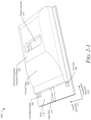
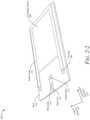
- FIGS. 2 - 1 through 2 - 3illustrate views of a vertical waveguide transition channel 202 .
- the vertical waveguide transition channel 202is an example of the vertical waveguide transition channel 112 of FIG. 1 .
- FIGS. 2 - 1 and 2 - 2include a reference coordinate system with a longitudinal direction 220 and a lateral direction 222 to indicate the relative positioning of aspects of the upward microstrip-to-waveguide transition.
- FIG. 2 - 1illustrates a top perspective view 200 - 1 of the vertical waveguide transition channel 202 .
- FIG. 2 - 2illustrates another top perspective view 200 - 2 of the vertical microstrip-to-waveguide transition without the vertical waveguide transition channel 202 to illustrate the components underneath.
- FIG. 2 - 3illustrates a side view of the vertical waveguide transition channel 202 with the waveguide 114 .
- the vertical microstrip-to-waveguide transitionwhich is illustrated in FIGS. 2 - 1 through 2 - 3 , includes the PCB 110 , the input port 116 , the vertical waveguide transition channel 202 , a grounding pattern 204 , and the waveguide 114 .
- the vertical waveguide transition channel 202can transition to a test port or other component.
- the PCB 110can include three or more dielectric layers, e.g., a first dielectric layer, a second dielectric layer, and a third dielectric layer.
- the input port 116 and the grounding pattern 204are part of the PCB 110 .
- the input port 116 and the grounding pattern 204can be formed on or as part of the first dielectric layer and be metal or a metal-plated microstrip.
- the input port 116includes a microstrip 214 that provides impedance matching to the feed lines from a MIMIC or other processor.
- the input port 116is placed near the short wall of the vertical waveguide transition channel 202 to efficiently excite the traveling electromagnetic wave inside a dielectric-filled cavity or portion of the vertical waveguide transition channel 202 .
- the grounding pattern 204encloses the bottom of the dielectric-filled cavity within the vertical waveguide transition channel 202 .
- the grounding pattern 204can be metal or a metal-plated material.
- the grounding pattern 204has an approximately rectangular cross-section with two arms extending in the longitudinal direction 220 toward the input port 116 on the lateral sides of the grounding pattern 204 .
- the rectangular cross-section of the grounding pattern 204approximately matches the dimensions of the dielectric-filled cavity formed by the interior of the vertical waveguide transition channel 202 .
- a width of the grounding pattern 204(e.g., in the lateral direction 222 ) matches or approximately matches the width of the vertical waveguide transition channel 202 .
- a length (e.g., in the longitudinal direction 220 ) of the grounding pattern 204 that includes both the rectangular cross-section and the armsis a small distance longer than the length of the vertical waveguide transition channel 202 .
- the extra length portion of the arms of the grounding pattern 204provides space for one of the via holes 206 that is not covered by the vertical waveguide transition channel 202 .
- the grounding pattern 204includes multiple via holes 206 to the second or third dielectric layer of the PCB 110 along its arms and the longitudinal edge of the rectangular cross-section nearest the input port 116 .
- the via holes 206form a via fence that together with the vertical waveguide transition channel 202 and the grounding pattern 204 enclose the dielectric-filled cavity within the vertical waveguide transition channel 202 .
- the via holes 206are generally closely spaced to form an equivalent wall to the electromagnetic waves excited by the input port 116 . In effect, the electromagnetic waves effectively see the collection of via holes 206 as a metal plate wall that is generally not feasible or is cost-prohibitive to create during PCB fabrication.
- the diameter and spacing of the via holes 206are designed to minimize or prevent energy leaking through the via fence, which would deteriorate the performance of the vertical microstrip-to-waveguide transition.
- the vertical waveguide transition channel 202includes a vertical taper 208 and an output aperture 210 .
- the vertical waveguide transition channel 202can be metal, a metal-plated material, or plastic.
- the vertical taper 208begins near the longitudinal edge of the vertical waveguide transition channel 202 nearest the input port 116 and gradually progresses toward the top surface. The taper allows the vertical waveguide transition channel 202 to transform from a microstrip mode at the input port 116 (quasi-transverse electromagnetic mode (TEM)) to waveguide mode at the waveguide 114 .
- TEMquadsi-transverse electromagnetic mode
- the vertical taper 208is designed to match an impedance of the waveguide 114 .
- the output aperture 210 of the vertical waveguide transition channel 202has an approximately rectangular shape and electromagnetic waves exit it in the waveguide mode.
- the output aperture 210can feed the waveguide 114 . In other implementations, the output aperture 210 can feed a test port.
- the dimensions of the vertical waveguide transition channel 202can be 6.3 millimeters (mm) in the longitudinal direction 220 , 3.7 mm in the lateral direction 222 , and 1 mm in a vertical direction with a thickness of 0.3 mm.
- the dimensions of the output aperture 210can be sized to approximately match the dimensions of an input aperture of the waveguide 114 .
- the output aperture 210is slightly smaller than the input aperture of the waveguide 114 (e.g., a WR10 waveguide) with dimensions of 2.13 mm in the lateral direction 222 and 0.74 mm in the longitudinal direction 220 .
- the vertical waveguide transition channel 202 and the output aperture 210are also possible.
- the dimensionscan be designed and selected to accommodate specific board layout requirements, MMIC-port topologies, and waveguide sizes, while maintaining impedance matching and low energy loss.
- the vertical waveguide transition channel 202is placed on the grounding pattern 204 .
- the vertical waveguide transition channel 202can be filled with various dielectrics, including air.
- the vertical waveguide transition channel 202can function as an air waveguide.
- the vertical waveguide transition channel 202can be mounted directly on the grounding pattern 204 .
- the vertical waveguide transition channel 202is mounted to the first surface using a surface-mount technology process, which can use a solder paste 212 or conductive epoxy.
- the input port 116In operation, energy from an MMIC (not illustrated in FIG. 2 ) or another processor is delivered to the input port 116 .
- the input port 116can have a supplier-defined or other arbitrary impedance (e.g., 100 ohms).
- the input port 116transmits the energy into the vertical waveguide transition channel 202 .
- the waveguide mode purityis high, which allows for a small air gap in the interface between the vertical waveguide transition channel 202 and the waveguide 114 .
- the vertical microstrip-to-waveguide transitioncan withstand up to 0.075-millimeter air gaps without a significant increase in the insertion loss or the return loss with a bandwidth of approximately 11 GHz.
- the described vertical microstrip-to-waveguide transitioncan tolerate up to 0.075-millimeter air gaps that are larger than a typical thickness of non-conductive pressure-sensitive adhesive, which is manufacturing efficient.
- the described vertical waveguide transition channel 202simplifies the attachment procedure for the waveguide 114 and allows for inexpensive and efficient manufacturing processes to complete the vertical microstrip-to-waveguide transition.
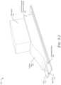
- FIGS. 3 - 1 and 3 - 2illustrate perspective views 300 - 1 and 300 - 2 , respectively, of another example upward microstrip-to-waveguide transition.
- a vertical waveguide transition channel 302is another example of the vertical waveguide transition channel 112 of FIG. 1 .
- the vertical microstrip-to-waveguide transitionincludes the PCB 110 , the input port 116 , the vertical waveguide transition channel 302 , the grounding pattern 204 , and a waveguide 304 .
- the waveguide 304includes the output aperture 118 that is in line with the longitudinal direction 220 .
- the dimensions of the vertical waveguide transition channel 302can be designed based on the dimensions of the waveguide 304 .
- FIG. 4illustrates an example method 400 for manufacturing a vertical microstrip-to-waveguide transition following techniques, apparatuses, and systems of this disclosure.
- Method 400is shown as sets of operations (or acts) performed, but not necessarily limited to the order or combinations in which the operations are shown herein. Further, any of one or more of the operations may be repeated, combined, or reorganized to provide other methods.
- referencemay be made to the environment 100 of FIG. 1 and entities detailed in FIGS. 1 through 3 - 2 , reference to which is made for example only.
- the techniquesare not limited to performance by one entity or multiple entities.
- a transition channelis formed that includes a vertical taper between a bottom surface and a top surface.
- the vertical waveguide transition channel 202can be stamped, etched, cut, machined, cast, molded, or formed in some other way.
- the vertical waveguide transition channel 202may be formed using a sheet-metal drawing process, which includes using tensile forces to stretch the metal material to a desired shape and thickness.
- the vertical waveguide transition channel 202may also be formed using a sheet-metal-stamping process, which includes applying pressure to the metal material by using a stamping press to form the desired shape and thickness. For complex shapes, the sheet-metal-stamping process may cost less than the sheet-metal-drawing process.
- the vertical waveguide transition channel 202may additionally be formed using a cast heatsink.
- the vertical waveguide transition channel 202can be metal or plastic.
- the vertical waveguide transition channel 202includes a bottom surface, a top surface, and the output aperture 210 in the top surface.
- the vertical waveguide transition channel 202includes a vertical taper between the bottom surface and the top surface.
- the output aperture 210has an approximately rectangular shape and can be sized to approximate the input aperture of the waveguide 114 .
- the waveguide 114can be mounted on the vertical waveguide transition channel 202 with an inlet aperture of the waveguide 114 being positioned over the output aperture 210 .
- the output aperture 118 of the waveguide 114can be in line with the lateral direction 222 (e.g., a lateral axis) or the longitudinal direction 220 (e.g., a longitudinal axis) of the vertical waveguide transition channel 202 .
- the waveguide 114can be operatively connected to an antenna input on another PCB.
- the vertical waveguide transition channel 202can withstand up to a 0.075-millimeter air gap at the interface between the waveguide 114 and the top surface of the vertical waveguide transition channel 202 .
- the vertical taper 208 of the vertical waveguide transition channel 202can be configured to match an impedance of the vertical waveguide transition channel 202 at the output aperture 210 with an impedance of the waveguide 114 .
- the thickness of the vertical waveguide transition channel 202can be approximately 0.3 millimeters.
- the vertical waveguide transition channel 202can have a length of approximately 6.3 millimeters in the longitudinal direction 220 , a width of approximately 3.7 millimeters in the lateral direction 222 , and a height of approximately one millimeter in a vertical direction perpendicular to the PCB 110 .
- the output aperture 210can have a width of approximately 2.13 millimeters in the lateral direction 222 and a length of approximately 0.74 millimeters in the longitudinal direction 220 .
- the transition channelis mounted on a grounding pattern that is located on a first surface of a PCB to form a dielectric-filled portion.
- the vertical waveguide transition channel 202is mounted directly on the grounding pattern 204 which is located a first surface of the PCB 110 , which can be a multi-layer PCB or a hybrid PCB stack-up.
- the vertical waveguide transition channel 202is mounted to the first surface using a surface-mount technology process, which can use a reflow process or conductive epoxy.
- the interior surface of the vertical waveguide transition channel 202along with the grounding pattern, form a dielectric-filled portion over the PCB 110 .
- the dielectric-filled portioncan be filled with air.
- the grounding pattern 204is made of a conductive material (e.g., a copper alloy).
- the grounding pattern 204has an approximately rectangular shape with two extensions extending in the longitudinal direction 220 .
- the grounding pattern 204also includes via holes to a second surface (e.g., a bottom surface), which is opposite the first surface of the PCB 110 .
- the PCB 110also includes a microstrip as part of the input port 116 on the first surface (e.g., the top surface of the PCB 110 ).
- the microstripis operatively connected to a processor (e.g., a MMIC) also located on the first surface of the PCB 110 and is configured to provide impedance matching to feed lines from the processor.
- a processore.g., a MMIC
- electromagnetic signalsare received or transmitted via the transition channel at or by an antenna operatively connected to the transition channel.
- the antennareceives or transmits electromagnetic signals that are routed via the vertical waveguide transition channel 202 through the radar system 102 to or from the MMIC.
Landscapes
- Engineering & Computer Science (AREA)
- Radar, Positioning & Navigation (AREA)
- Remote Sensing (AREA)
- Computer Networks & Wireless Communication (AREA)
- Physics & Mathematics (AREA)
- General Physics & Mathematics (AREA)
- Radar Systems Or Details Thereof (AREA)
Abstract
Description
Claims (20)
Priority Applications (3)
| Application Number | Priority Date | Filing Date | Title |
|---|---|---|---|
| US17/804,061US12265172B2 (en) | 2022-05-25 | 2022-05-25 | Vertical microstrip-to-waveguide transition |
| EP23163662.2AEP4283777A1 (en) | 2022-05-25 | 2023-03-23 | Vertical microstrip-to-waveguide transition |
| CN202310582117.4ACN117134088A (en) | 2022-05-25 | 2023-05-22 | Vertical microstrip waveguide transition |
Applications Claiming Priority (1)
| Application Number | Priority Date | Filing Date | Title |
|---|---|---|---|
| US17/804,061US12265172B2 (en) | 2022-05-25 | 2022-05-25 | Vertical microstrip-to-waveguide transition |
Publications (2)
| Publication Number | Publication Date |
|---|---|
| US20230384414A1 US20230384414A1 (en) | 2023-11-30 |
| US12265172B2true US12265172B2 (en) | 2025-04-01 |
Family
ID=85726630
Family Applications (1)
| Application Number | Title | Priority Date | Filing Date |
|---|---|---|---|
| US17/804,061Active2043-07-12US12265172B2 (en) | 2022-05-25 | 2022-05-25 | Vertical microstrip-to-waveguide transition |
Country Status (3)
| Country | Link |
|---|---|
| US (1) | US12265172B2 (en) |
| EP (1) | EP4283777A1 (en) |
| CN (1) | CN117134088A (en) |
Citations (219)
| Publication number | Priority date | Publication date | Assignee | Title |
|---|---|---|---|---|
| US2840818A (en) | 1954-04-15 | 1958-06-24 | Hughes Aircraft Co | Slotted antenna |
| US3462713A (en) | 1967-07-19 | 1969-08-19 | Bell Telephone Labor Inc | Waveguide-stripline transducer |
| US3579149A (en) | 1969-12-08 | 1971-05-18 | Westinghouse Electric Corp | Waveguide to stripline transition means |
| US4157516A (en) | 1976-09-07 | 1979-06-05 | U.S. Philips Corporation | Wave guide to microstrip transition |
| US4453142A (en) | 1981-11-02 | 1984-06-05 | Motorola Inc. | Microstrip to waveguide transition |
| US4562416A (en) | 1984-05-31 | 1985-12-31 | Sanders Associates, Inc. | Transition from stripline to waveguide |
| US5065123A (en) | 1990-10-01 | 1991-11-12 | Harris Corporation | Waffle wall-configured conducting structure for chip isolation in millimeter wave monolithic subsystem assemblies |
| DE4241635A1 (en) | 1992-12-10 | 1994-06-16 | Ant Nachrichtentech | Transition piece between microstrip waveguide to hollow waveguide - broadens from microstrip into unilateral suspended substrate guide to match and join hollow guide |
| US5350499A (en) | 1990-09-17 | 1994-09-27 | Matsushita Electric Industrial Co., Ltd. | Method of producing microscopic structure |
| US5414394A (en) | 1992-12-29 | 1995-05-09 | U.S. Philips Corporation | Microwave frequency device comprising at least a transition between a transmission line integrated on a substrate and a waveguide |
| US5637521A (en) | 1996-06-14 | 1997-06-10 | The United States Of America As Represented By The Secretary Of The Army | Method of fabricating an air-filled waveguide on a semiconductor body |
| US5923225A (en) | 1997-10-03 | 1999-07-13 | De Los Santos; Hector J. | Noise-reduction systems and methods using photonic bandgap crystals |
| US5929728A (en) | 1997-06-25 | 1999-07-27 | Hewlett-Packard Company | Imbedded waveguide structures for a microwave circuit package |
| US5982256A (en) | 1997-04-22 | 1999-11-09 | Kyocera Corporation | Wiring board equipped with a line for transmitting a high frequency signal |
| US5982250A (en) | 1997-11-26 | 1999-11-09 | Twr Inc. | Millimeter-wave LTCC package |
| US5986527A (en) | 1995-03-28 | 1999-11-16 | Murata Manufacturing Co., Ltd. | Planar dielectric line and integrated circuit using the same line |
| US6064350A (en) | 1997-07-25 | 2000-05-16 | Kyocera Corporation | Laminated aperture-faced antenna and multi-layered wiring board comprising the same |
| US6072375A (en) | 1998-05-12 | 2000-06-06 | Harris Corporation | Waveguide with edge grounding |
| US6127901A (en) | 1999-05-27 | 2000-10-03 | Hrl Laboratories, Llc | Method and apparatus for coupling a microstrip transmission line to a waveguide transmission line for microwave or millimeter-wave frequency range transmission |
| JP2000357916A (en) | 1999-06-15 | 2000-12-26 | Kobe Steel Ltd | Waveguide slot array antenna |
| US20020021197A1 (en)* | 1999-10-29 | 2002-02-21 | Berg Technology, Inc. | Waveguides and backplane systems |
| US6414573B1 (en) | 2000-02-16 | 2002-07-02 | Hughes Electronics Corp. | Stripline signal distribution system for extremely high frequency signals |
| US6489855B1 (en) | 1998-12-25 | 2002-12-03 | Murata Manufacturing Co. Ltd | Line transition device between dielectric waveguide and waveguide, and oscillator, and transmitter using the same |
| US6535083B1 (en) | 2000-09-05 | 2003-03-18 | Northrop Grumman Corporation | Embedded ridge waveguide filters |
| KR20030031585A (en) | 2001-10-15 | 2003-04-23 | (주)지앤티웍스 | Fabrication method of double-sided dielectric PCB on waveguide for slotted waveguide array antennas |
| JP2003243902A (en) | 2002-02-18 | 2003-08-29 | Alps Electric Co Ltd | Converter for receiving satellite broadcast |
| US6622370B1 (en) | 2000-04-13 | 2003-09-23 | Raytheon Company | Method for fabricating suspended transmission line |
| JP2003289201A (en) | 2002-03-28 | 2003-10-10 | Anritsu Corp | Post-wall waveguide and junction conversion structure for cavity waveguide |
| US6658233B1 (en) | 1999-10-04 | 2003-12-02 | Alps Electric Co., Ltd. | Satellite broadcast receiving converter |
| US20040069984A1 (en) | 2001-05-21 | 2004-04-15 | Estes Michael J. | Terahertz interconnect system and applications |
| US6788918B2 (en) | 2001-01-12 | 2004-09-07 | Murata Manufacturing Co., Ltd. | Transmission line assembly, integrated circuit, and transmitter-receiver apparatus comprising a dielectric waveguide protuding for a dielectric plate |
| US6794950B2 (en) | 2000-12-21 | 2004-09-21 | Paratek Microwave, Inc. | Waveguide to microstrip transition |
| US6859114B2 (en) | 2002-05-31 | 2005-02-22 | George V. Eleftheriades | Metamaterials for controlling and guiding electromagnetic radiation and applications therefor |
| CN1620738A (en) | 2000-10-18 | 2005-05-25 | 诺基亚公司 | Waveguide to Stripline Transition |
| CN1682404A (en) | 2002-09-20 | 2005-10-12 | 伊兹德国有限公司 | Junction between a microstrip line and a waveguide |
| US6995726B1 (en) | 2004-07-15 | 2006-02-07 | Rockwell Collins | Split waveguide phased array antenna with integrated bias assembly |
| US20060113598A1 (en) | 2004-11-16 | 2006-06-01 | Chen Howard H | Device and method for fabricating double-sided SOI wafer scale package with optical through via connections |
| CN2796131Y (en) | 2005-05-30 | 2006-07-12 | 东南大学 | Multilayer substrate integrated wave guide elliptical response filter |
| US7142165B2 (en) | 2002-01-29 | 2006-11-28 | Era Patents Limited | Waveguide and slotted antenna array with moveable rows of spaced posts |
| JP3923360B2 (en) | 2002-04-26 | 2007-05-30 | 三菱電機株式会社 | Slot array antenna and slot array antenna apparatus |
| US7276988B2 (en) | 2004-06-30 | 2007-10-02 | Endwave Corporation | Multi-substrate microstrip to waveguide transition |
| CA2654470A1 (en) | 2006-06-12 | 2007-12-27 | Pacific Biosciences Of California, Inc. | Substrates for performing analytical reactions |
| KR20080044752A (en) | 2006-11-17 | 2008-05-21 | 한국전자통신연구원 | Millimeter wave transition device of dielectric waveguide vs transmission line |
| US20080129409A1 (en) | 2006-11-30 | 2008-06-05 | Hideyuki Nagaishi | Waveguide structure |
| US20080150821A1 (en) | 2006-12-22 | 2008-06-26 | Sony Deutschland Gmbh | Flexible substrate integrated waveguides |
| US7420442B1 (en) | 2005-06-08 | 2008-09-02 | Sandia Corporation | Micromachined microwave signal control device and method for making same |
| US7439822B2 (en) | 2005-06-06 | 2008-10-21 | Fujitsu Limited | Waveguide substrate having two slit-like couplings and high-frequency circuit module |
| US20090040132A1 (en) | 2007-07-24 | 2009-02-12 | Northeastern University | Anisotropic metal-dielectric metamaterials for broadband all-angle negative refraction and superlens imaging |
| US7495532B2 (en) | 2004-03-08 | 2009-02-24 | Wemtec, Inc. | Systems and methods for blocking microwave propagation in parallel plate structures |
| US20090207090A1 (en) | 2007-06-22 | 2009-08-20 | Vubiq Incorporated | Integrated antenna and chip package and method of manufacturing thereof |
| US20090243762A1 (en) | 2008-03-27 | 2009-10-01 | Xiao-Ping Chen | Waveguide filter |
| US7626476B2 (en) | 2006-04-13 | 2009-12-01 | Electronics And Telecommunications Research Institute | Multi-metal coplanar waveguide |
| CN201383535Y (en) | 2009-04-01 | 2010-01-13 | 惠州市硕贝德通讯科技有限公司 | Rectangular waveguide-substrate integrated waveguide signal conversion and power divider |
| US7659799B2 (en) | 2005-11-25 | 2010-02-09 | Electronics And Telecommunications Research Institute | Dielectric waveguide filter with cross-coupling |
| US20100193935A1 (en) | 2009-01-30 | 2010-08-05 | Infineon Technologies Ag | Integrated antennas in wafer level package |
| US20110001579A1 (en)* | 2007-11-28 | 2011-01-06 | Vincenzo Boffa | Tunable ridge waveguide delay line |
| US20110140810A1 (en) | 2009-09-08 | 2011-06-16 | Siklu Communication ltd. | Waveguide-backshort comprising a printed conducting layer |
| US20110140979A1 (en) | 2009-09-08 | 2011-06-16 | Siklu Communication ltd. | Waveguide comprising laminate structure |
| US7973616B2 (en) | 2008-06-05 | 2011-07-05 | Kabushiki Kaisha Toshiba | Post-wall waveguide based short slot directional coupler, butler matrix using the same and automotive radar antenna |
| US8013694B2 (en) | 2006-03-31 | 2011-09-06 | Kyocera Corporation | Dielectric waveguide device, phase shifter, high frequency switch, and attenuator provided with dielectric waveguide device, high frequency transmitter, high frequency receiver, high frequency transceiver, radar device, array antenna, and method of manufacturing dielectric waveguide device |
| US8089327B2 (en) | 2009-03-09 | 2012-01-03 | Toyota Motor Engineering & Manufacturing North America, Inc. | Waveguide to plural microstrip transition |
| US20120013421A1 (en) | 2009-03-31 | 2012-01-19 | Kyocera Corporation | Waveguide Structure, High Frequency Module Including Waveguide Structure, and Radar Apparatus |
| US20120050125A1 (en) | 2010-08-31 | 2012-03-01 | Siklu Communication ltd. | Systems for interfacing waveguide antenna feeds with printed circuit boards |
| US20120068316A1 (en) | 2009-05-08 | 2012-03-22 | Telefonaktiebolaget L M Ericsson (Publ) | Transition from a chip to a waveguide port |
| US8159316B2 (en) | 2007-12-28 | 2012-04-17 | Kyocera Corporation | High-frequency transmission line connection structure, circuit board, high-frequency module, and radar device |
| US20120163811A1 (en) | 2007-03-26 | 2012-06-28 | International Business Machines Corporation | Ultra-high bandwidth, multiple-channel full-duplex, single-chip cmos optical transceiver |
| EP2500978A1 (en) | 2011-03-17 | 2012-09-19 | Sivers Ima AB | Waveguide transition |
| CN102696145A (en) | 2009-12-07 | 2012-09-26 | 卡西迪安有限公司 | Microwave transition device between a microstrip line and a rectangular waveguide |
| US20120256796A1 (en) | 2010-08-31 | 2012-10-11 | Siklu Communication ltd. | Compact millimeter-wave radio systems and methods |
| US20120256707A1 (en) | 2011-02-21 | 2012-10-11 | Siklu Communication ltd. | Systems and methods for millimeter-wave laminate structures |
| GB2489950A (en) | 2011-04-12 | 2012-10-17 | Filtronic Plc | A substrate integrated waveguide (SIW) to air filled waveguide transition comprising a tapered dielectric layer |
| US20130057358A1 (en) | 2011-09-02 | 2013-03-07 | Theodore K. Anthony | Waveguide to Co-Planar-Waveguide (CPW) ransition |
| US8395552B2 (en) | 2010-11-23 | 2013-03-12 | Metamagnetics, Inc. | Antenna module having reduced size, high gain, and increased power efficiency |
| US8451189B1 (en) | 2009-04-15 | 2013-05-28 | Herbert U. Fluhler | Ultra-wide band (UWB) artificial magnetic conductor (AMC) metamaterials for electrically thin antennas and arrays |
| US8451175B2 (en) | 2008-03-25 | 2013-05-28 | Tyco Electronics Services Gmbh | Advanced active metamaterial antenna systems |
| US20130256849A1 (en) | 2012-03-29 | 2013-10-03 | International Business Machines Corporation | High frequency transition matching in an electronic package for millimeter wave semiconductor dies |
| WO2013189513A1 (en) | 2012-06-18 | 2013-12-27 | Huawei Technologies Co., Ltd. | Directional coupler waveguide structure and method |
| CN103515682A (en) | 2013-07-24 | 2014-01-15 | 中国电子科技集团公司第五十五研究所 | Micro-strip-to-waveguide vertical transition structure achieved through multi-layer step type substrate integration waveguide |
| US20140015709A1 (en) | 2012-07-13 | 2014-01-16 | Kabushiki Kaisha Toshiba | Waveguide connecting structure, antenna device and radar device |
| US20140048310A1 (en) | 2012-08-16 | 2014-02-20 | Apple Inc. | Printed Circuit Solder Connections |
| US8680936B2 (en) | 2011-11-18 | 2014-03-25 | Delphi Technologies, Inc. | Surface mountable microwave signal transition block for microstrip to perpendicular waveguide transition |
| US8692731B2 (en) | 2011-02-16 | 2014-04-08 | Samsung Electro-Mechanics Co., Ltd. | Dielectric waveguide antenna |
| US20140106684A1 (en) | 2012-10-15 | 2014-04-17 | Qualcomm Mems Technologies, Inc. | Transparent antennas on a display device |
| US8717124B2 (en) | 2010-01-22 | 2014-05-06 | Nuvotronics, Llc | Thermal management |
| US8803638B2 (en) | 2008-07-07 | 2014-08-12 | Kildal Antenna Consulting Ab | Waveguides and transmission lines in gaps between parallel conducting surfaces |
| US20140287703A1 (en)* | 2013-03-19 | 2014-09-25 | Texas Instruments Incorporated | Integrated Circuit with Antenna for Dielectric Waveguide |
| US8948562B2 (en) | 2008-11-25 | 2015-02-03 | Regents Of The University Of Minnesota | Replication of patterned thin-film structures for use in plasmonics and metamaterials |
| EP2843758A1 (en) | 2013-08-27 | 2015-03-04 | Microelectronics Technology Inc. | Multi-layer circuit board with waveguide to microstrip transition structure |
| US20150097633A1 (en) | 2013-10-08 | 2015-04-09 | Blackberry Limited | 60 ghz integrated circuit to printed circuit board transitions |
| US20150229017A1 (en) | 2014-02-07 | 2015-08-13 | Fujitsu Limited | High frequency module and fabrication method for high frequency module |
| CN104900956A (en) | 2015-05-06 | 2015-09-09 | 东南大学 | Device for switching waveguide to substrate integrated waveguide |
| US20150295297A1 (en) | 2014-04-09 | 2015-10-15 | Texas Instruments Incorporated | Metallic Waveguide with Dielectric Core |
| EP2945222A1 (en) | 2014-05-14 | 2015-11-18 | Gapwaves AB | A microwave or millimeter wave RF part using pin grid array (PGA) and/or ball grid array (BGA) technologies |
| CN105098295A (en) | 2014-05-16 | 2015-11-25 | 香港城市大学 | Apparatus and method for electromagnetic signal conversion |
| US9203155B2 (en) | 2011-06-27 | 2015-12-01 | Electronics And Telecommunications Research Institute | Metamaterial structure and manufacturing method of the same |
| US20150357698A1 (en)* | 2013-01-10 | 2015-12-10 | Nec Corporation | Wideband transition between a planar transmission line and a waveguide |
| US20150364830A1 (en) | 2014-06-13 | 2015-12-17 | Freescale Semiconductor, Inc. | Integrated circuit package with radio frequency coupling structure |
| US20150364804A1 (en) | 2014-06-13 | 2015-12-17 | Freescale Semiconductor, Inc. | Radio frequency coupling structure |
| US9246204B1 (en) | 2012-01-19 | 2016-01-26 | Hrl Laboratories, Llc | Surface wave guiding apparatus and method for guiding the surface wave along an arbitrary path |
| US9258884B2 (en) | 2012-05-17 | 2016-02-09 | Canon Kabushiki Kaisha | Suppression of current component using EBG structure |
| US20160043455A1 (en) | 2014-08-07 | 2016-02-11 | Infineon Technologies Ag | Microwave Chip Package Device |
| US20160049714A1 (en) | 2013-03-24 | 2016-02-18 | TELEFONAKTIEBOLAGET L.M.ERICSSON (publ) | Transition Between a SIW and a Waveguide Interface |
| US20160056541A1 (en) | 2013-03-24 | 2016-02-25 | Telefonaktiebolaget L M Ericsson (Publ) | A siw antenna arrangement |
| US20160111764A1 (en) | 2014-10-16 | 2016-04-21 | Hyundai Mobis Co., Ltd. | Transit structure of waveguide and siw |
| US20160118705A1 (en) | 2014-10-23 | 2016-04-28 | Freescale Semiconductor, Inc. | Packaged integrated circuit waveguide interface and methods thereof |
| CN105609909A (en) | 2016-03-08 | 2016-05-25 | 电子科技大学 | Device for transition from rectangular waveguide to substrate integrated waveguide on Ka-band |
| CN105680133A (en) | 2016-01-11 | 2016-06-15 | 中国电子科技集团公司第十研究所 | Inter-board perpendicular interconnection circuit structure for substrate integrated ridge waveguide |
| US20160204495A1 (en) | 2013-10-01 | 2016-07-14 | Sony Corporation | Connector apparatus and communication system |
| CN105958167A (en) | 2016-07-01 | 2016-09-21 | 北京交通大学 | Vertical substrate integrated waveguide and vertical connection structure comprising the waveguide |
| US20160276727A1 (en) | 2015-03-19 | 2016-09-22 | International Business Machines Corporation | Package structures having integrated waveguides for high speed communications between package components |
| US20160293557A1 (en) | 2015-03-30 | 2016-10-06 | Sony Corporation | Package and antenna apparatus including package |
| US20160301125A1 (en) | 2015-04-13 | 2016-10-13 | Research & Business Foundation Sungkyunkwan University | On-chip waveguide feeder for millimiter wave ics and feeding methods, and multiple input and output millimeter wave transceiver system using same |
| US20170084554A1 (en) | 2015-09-21 | 2017-03-23 | Intel Corporation | Platform with thermally stable wireless interconnects |
| US20170099705A1 (en) | 2014-05-26 | 2017-04-06 | Electrolux Appliances Aktiebolag | Microwave oven with a waveguide including a reflector element |
| US9647313B2 (en) | 2012-01-19 | 2017-05-09 | Huawei Technologies Co., Ltd. | Surface mount microwave system including a transition between a multilayer arrangement and a hollow waveguide |
| US9653773B2 (en) | 2012-04-24 | 2017-05-16 | Universite Grenoble Alpes | Slow wave RF propagation line including a network of nanowires |
| CN106711616A (en) | 2016-12-30 | 2017-05-24 | 广东盛路通信科技股份有限公司 | Planar slot array antenna |
| CN106785424A (en) | 2016-11-29 | 2017-05-31 | 大连港森立达木材交易中心有限公司 | The two-way Uniform Irradiation antenna-feedback system of High-Power Microwave |
| US9673532B2 (en) | 2013-07-31 | 2017-06-06 | Huawei Technologies Co., Ltd. | Antenna |
| US9806393B2 (en) | 2012-06-18 | 2017-10-31 | Gapwaves Ab | Gap waveguide structures for THz applications |
| US9813042B2 (en) | 2015-08-28 | 2017-11-07 | City University Of Hong Kong | Converting a single-ended signal to a differential signal |
| US20170324135A1 (en) | 2014-12-12 | 2017-11-09 | Sony Corporation | Microwave antenna apparatus, packing and manufacturing method |
| US9843301B1 (en) | 2016-07-14 | 2017-12-12 | Northrop Grumman Systems Corporation | Silicon transformer balun |
| WO2018003932A1 (en) | 2016-06-29 | 2018-01-04 | Nidec Elesys Corporation | Waveguide device module and microwave module |
| DE102016213202A1 (en) | 2016-07-19 | 2018-01-25 | Conti Temic Microelectronic Gmbh | Multi-layer board with a transition element for transforming a waveguide shaft onto a conducted shaft |
| US9935065B1 (en) | 2016-12-21 | 2018-04-03 | Infineon Technologies Ag | Radio frequency device packages and methods of formation thereof |
| US9947981B1 (en) | 2016-05-19 | 2018-04-17 | National Technology & Engineering Solutions of Sandian, LLC | Waveguide module comprising a first plate with a waveguide channel and a second plate with a raised portion in which a sealing layer is forced into the waveguide channel by the raised portion |
| US20180131084A1 (en) | 2016-11-08 | 2018-05-10 | Korea Advanced Institute Of Science And Technology | Printed-circuit board having antennas and electromagnetic-tunnel-embedded architecture and manufacturing method thereof |
| WO2018095541A1 (en) | 2016-11-25 | 2018-05-31 | Jianyang Antenna&Microwaves | Planar array antenna |
| US9991606B2 (en) | 2015-11-05 | 2018-06-05 | Nidec Corporation | Slot array antenna |
| US10027032B2 (en) | 2015-10-15 | 2018-07-17 | Nidec Corporation | Waveguide device and antenna device including the waveguide device |
| US10042045B2 (en) | 2016-01-15 | 2018-08-07 | Nidec Corporation | Waveguide device, slot array antenna, and radar, radar system, and wireless communication system including the slot array antenna |
| US20180226709A1 (en) | 2017-02-08 | 2018-08-09 | Delphi Technologies, Inc. | Radar assembly with ultra wide band waveguide to substrate integrated waveguide transition |
| US20180226727A1 (en) | 2017-02-07 | 2018-08-09 | Panasonic Corporation | Module, wireless communication apparatus, and radar apparatus |
| US20180233465A1 (en) | 2017-02-15 | 2018-08-16 | Nxp B.V. | Integrated circuit package |
| US10090600B2 (en) | 2016-02-12 | 2018-10-02 | Nidec Corporation | Waveguide device, and antenna device including the waveguide device |
| US20180284186A1 (en) | 2017-04-03 | 2018-10-04 | Nvidia Corporation | Multi-chip package with selection logic and debug ports for testing inter-chip communications |
| US20180301816A1 (en) | 2017-04-18 | 2018-10-18 | Nidec Corporation | Slot array antenna |
| US10114067B2 (en) | 2016-02-04 | 2018-10-30 | Advantest Corporation | Integrated waveguide structure and socket structure for millimeter waveband testing |
| US20180343711A1 (en) | 2017-05-24 | 2018-11-29 | Miele & Cie. Kg | Device for generating and transmitting high-frequency waves (hf waves) |
| US20180351261A1 (en) | 2017-06-05 | 2018-12-06 | Nidec Corporation | Waveguide device, and antenna device including the waveguide device |
| US10153533B2 (en) | 2014-05-07 | 2018-12-11 | Hideki Kirino | Waveguide |
| US10158158B2 (en) | 2016-02-08 | 2018-12-18 | Nidec Corporation | Waveguide device, and antenna device including the waveguide device |
| US10164318B2 (en) | 2012-10-22 | 2018-12-25 | Texas Instruments Incorporated | Waveguide coupler |
| US10164344B2 (en) | 2015-12-24 | 2018-12-25 | Nidec Corporation | Waveguide device, slot antenna, and radar, radar system, and wireless communication system including the slot antenna |
| US20180375185A1 (en) | 2017-06-26 | 2018-12-27 | WGR Co., Ltd. | Electromagnetic wave transmission device |
| US20190006743A1 (en) | 2017-06-30 | 2019-01-03 | Nidec Corporation | Waveguide device module, microwave module, radar device, and radar system |
| US20190013563A1 (en) | 2016-01-20 | 2019-01-10 | Sony Corporation | Connector module, communication circuit board, and electronic device |
| EP3460903A1 (en) | 2017-09-20 | 2019-03-27 | Aptiv Technologies Limited | Antenna device with direct differential input useable on an automated vehicle |
| US10263310B2 (en) | 2014-05-14 | 2019-04-16 | Gapwaves Ab | Waveguides and transmission lines in gaps between parallel conducting surfaces |
| CN109716861A (en) | 2016-09-19 | 2019-05-03 | Sp系列有限公司 | Micro-wave oven and its Radiation Module |
| WO2019085368A1 (en) | 2017-10-31 | 2019-05-09 | 深圳市华讯方舟微电子科技有限公司 | Wilkinson power divider |
| CN109750201A (en) | 2019-02-22 | 2019-05-14 | 中国科学院长春应用化学研究所 | Micro-alloyed magnesium alloy sheet with high formability and preparation method thereof |
| US10312596B2 (en) | 2013-01-17 | 2019-06-04 | Hrl Laboratories, Llc | Dual-polarization, circularly-polarized, surface-wave-waveguide, artificial-impedance-surface antenna |
| US20190194452A1 (en) | 2016-08-22 | 2019-06-27 | Mep Europe B.V. | Thermoplastic composition for laser direct structuring |
| US20190207286A1 (en) | 2017-12-30 | 2019-07-04 | Texas Instruments Incorporated | Printed circuit board with substrate-integrated waveguide transition |
| US10374323B2 (en) | 2017-03-24 | 2019-08-06 | Nidec Corporation | Slot array antenna and radar having the slot array antenna |
| US10381741B2 (en) | 2015-12-24 | 2019-08-13 | Nidec Corporation | Slot array antenna, and radar, radar system, and wireless communication system including the slot array antenna |
| US10381317B2 (en) | 2016-02-12 | 2019-08-13 | Telefonaktiebolaget Lm Ericsson (Publ) | Transition arrangement comprising a contactless transition or connection between an SIW and a waveguide or an antenna |
| CN209389219U (en) | 2019-02-25 | 2019-09-13 | 贵州航天电子科技有限公司 | A kind of Waveguide slot array antenna structure suitable for increasing material manufacturing |
| US10505282B2 (en) | 2016-08-10 | 2019-12-10 | Microsoft Technology Licensing, Llc | Dielectric groove waveguide |
| US10534061B2 (en) | 2015-04-08 | 2020-01-14 | Gapwaves Ab | Calibration arrangement and a method for a microwave analyzing or measuring instrument |
| US10594045B2 (en) | 2016-04-05 | 2020-03-17 | Nidec Corporation | Waveguide device and antenna array |
| US10601144B2 (en) | 2017-04-13 | 2020-03-24 | Nidec Corporation | Slot antenna device |
| US10608345B2 (en) | 2017-04-13 | 2020-03-31 | Nidec Corporation | Slot array antenna |
| US10622696B2 (en) | 2017-09-07 | 2020-04-14 | Nidec Corporation | Directional coupler |
| US10651138B2 (en) | 2016-03-29 | 2020-05-12 | Nidec Corporation | Microwave IC waveguide device module |
| US10651567B2 (en) | 2017-06-26 | 2020-05-12 | Nidec Corporation | Method of producing a horn antenna array and antenna array |
| US20200153108A1 (en) | 2017-07-06 | 2020-05-14 | Fujikura Ltd. | Waveguide slot array antenna |
| US10658760B2 (en) | 2017-06-26 | 2020-05-19 | Nidec Corporation | Horn antenna array |
| US10670810B2 (en) | 2017-12-22 | 2020-06-02 | Huawei Technologies Canada Co., Ltd. | Polarization selective coupler |
| US10705294B2 (en) | 2018-03-15 | 2020-07-07 | Stmicroelectronics (Crolles 2) Sas | Waveguide termination device |
| US10707584B2 (en) | 2017-08-18 | 2020-07-07 | Nidec Corporation | Antenna array |
| US20200220273A1 (en) | 2019-01-04 | 2020-07-09 | Veoneer Us, Inc. | System and Method with Multilayer Laminated Waveguide Antenna |
| US10714802B2 (en) | 2017-06-26 | 2020-07-14 | WGR Co., Ltd. | Transmission line device |
| US20200235453A1 (en) | 2019-01-21 | 2020-07-23 | Infineon Technologies Ag | Method for producing a waveguide, circuit device and radar system |
| US10727561B2 (en) | 2016-04-28 | 2020-07-28 | Nidec Corporation | Mounting substrate, waveguide module, integrated circuit-mounted substrate, microwave module |
| US20200241107A1 (en) | 2019-01-29 | 2020-07-30 | Magna Electronics Inc. | Sensing system with enhanced electrical contact at pcb-waveguide interface |
| US10763590B2 (en) | 2015-11-05 | 2020-09-01 | Nidec Corporation | Slot antenna |
| US20200287293A1 (en) | 2019-03-06 | 2020-09-10 | Aptiv Technologies Limited | Slot array antenna including parasitic features |
| US10775573B1 (en) | 2019-04-03 | 2020-09-15 | International Business Machines Corporation | Embedding mirror with metal particle coating |
| US10811373B2 (en) | 2016-10-05 | 2020-10-20 | Gapwaves Ab | Packaging structure comprising at least one transition forming a contactless interface |
| US20200343612A1 (en) | 2019-04-29 | 2020-10-29 | Aptiv Technologies Limited | Wave guide launcher |
| US10826147B2 (en) | 2017-11-10 | 2020-11-03 | Raytheon Company | Radio frequency circuit with a multi-layer transmission line assembly having a conductively filled trench surrounding the transmission line |
| US10833382B2 (en) | 2015-09-25 | 2020-11-10 | Bae Systems Australia Limited | RF structure and a method of forming an RF structure |
| US20200388899A1 (en) | 2019-06-10 | 2020-12-10 | Hughes Network Systems, Llc | Microstrip-to-waveguide transition and radio assembly |
| US20200412012A1 (en)* | 2019-06-26 | 2020-12-31 | Honeywell International Inc. | Fixing structure to enhance the mechanical reliability of plate slot array antenna based on siw technology |
| US10892536B2 (en) | 2015-09-24 | 2021-01-12 | Gapwaves Ab | Waveguides and transmission lines in gaps between parallel conducting surfaces |
| US20210028549A1 (en) | 2019-07-23 | 2021-01-28 | Veoneer Us, Inc. | Combined waveguide and antenna structures and related sensor assemblies |
| US10957971B2 (en) | 2019-07-23 | 2021-03-23 | Veoneer Us, Inc. | Feed to waveguide transition structures and related sensor assemblies |
| US10971824B2 (en) | 2016-09-30 | 2021-04-06 | Ims Connector Systems Gmbh | Antenna element |
| US10985434B2 (en) | 2017-01-24 | 2021-04-20 | Huber+Suhner Ag | Waveguide assembly including a waveguide element and a connector body, where the connector body includes recesses defining electromagnetic band gap elements therein |
| US10983194B1 (en) | 2014-06-12 | 2021-04-20 | Hrl Laboratories, Llc | Metasurfaces for improving co-site isolation for electronic warfare applications |
| US10992056B2 (en) | 2017-04-14 | 2021-04-27 | Nidec Corporation | Slot antenna device |
| US20210159577A1 (en) | 2016-05-03 | 2021-05-27 | Gapwaves Ab | Arrangement for interconnection of waveguide structures and a structure for a waveguide structure interconnecting arrangement |
| WO2021122725A1 (en) | 2019-12-20 | 2021-06-24 | Gapwaves Ab | An antenna arrangement with a low-ripple radiation pattern |
| US11061110B2 (en) | 2017-05-11 | 2021-07-13 | Nidec Corporation | Waveguide device, and antenna device including the waveguide device |
| US11088464B2 (en) | 2018-06-14 | 2021-08-10 | Nidec Corporation | Slot array antenna |
| US11114733B2 (en) | 2019-07-23 | 2021-09-07 | Veoneer Us, Inc. | Waveguide interconnect transitions and related sensor assemblies |
| US11121475B2 (en) | 2017-09-25 | 2021-09-14 | Gapwaves Ab | Phased array antenna |
| US20210305667A1 (en) | 2018-09-04 | 2021-09-30 | Gapwaves Ab | High frequency filter and phased array antenna comprising such a high frequency filter |
| US11171399B2 (en) | 2019-07-23 | 2021-11-09 | Veoneer Us, Inc. | Meandering waveguide ridges and related sensor assemblies |
| US11169325B2 (en) | 2018-03-15 | 2021-11-09 | Stmicroelectronics (Crolles 2) Sas | Filtering device in a waveguide |
| US20210367352A1 (en) | 2016-07-11 | 2021-11-25 | Waymo Llc | Radar antenna array with parasitic elements excited by surface waves |
| US11201414B2 (en) | 2018-12-18 | 2021-12-14 | Veoneer Us, Inc. | Waveguide sensor assemblies and related methods |
| US11249011B2 (en) | 2016-10-19 | 2022-02-15 | Global Life Sciences Solutions Usa Llc | Apparatus and method for evanescent waveguide sensing |
| US11283162B2 (en)* | 2019-07-23 | 2022-03-22 | Veoneer Us, Inc. | Transitional waveguide structures and related sensor assemblies |
| US11289787B2 (en) | 2017-10-25 | 2022-03-29 | Gapwaves Ab | Transition arrangement comprising a waveguide twist, a waveguide structure comprising a number of waveguide twists and a rotary joint |
| US20220109246A1 (en) | 2019-02-08 | 2022-04-07 | Gapwaves Ab | Antenna array based on one or more metamaterial structures |
| US20220140488A1 (en)* | 2020-10-29 | 2022-05-05 | Robert Bosch Gmbh | High-frequency circuit including a circuit board and a waveguide structure |
| US11349220B2 (en) | 2020-02-12 | 2022-05-31 | Veoneer Us, Inc. | Oscillating waveguides and related sensor assemblies |
| US11349183B2 (en) | 2017-11-07 | 2022-05-31 | Rise Research Institutes of Sweden AB | Contactless waveguide switch and method for manufacturing a waveguide switch |
| US11378683B2 (en) | 2020-02-12 | 2022-07-05 | Veoneer Us, Inc. | Vehicle radar sensor assemblies |
| US11411292B2 (en) | 2019-01-16 | 2022-08-09 | WGR Co., Ltd. | Waveguide device, electromagnetic radiation confinement device, antenna device, microwave chemical reaction device, and radar device |
| US11495871B2 (en) | 2017-10-27 | 2022-11-08 | Metasum Ab | Waveguide device having multiple layers, where through going empty holes are in each layer and are offset in adjoining layers for leakage suppression |
| US11563259B2 (en) | 2020-02-12 | 2023-01-24 | Veoneer Us, Llc | Waveguide signal confinement structures and related sensor assemblies |
| US11611138B2 (en) | 2017-04-12 | 2023-03-21 | Nidec Corporation | Method of producing a radio frequency member |
| US11616306B2 (en) | 2021-03-22 | 2023-03-28 | Aptiv Technologies Limited | Apparatus, method and system comprising an air waveguide antenna having a single layer material with air channels therein which is interfaced with a circuit board |
| US11626652B2 (en) | 2018-12-06 | 2023-04-11 | Samsung Electronics Co., Ltd | Ridge gap waveguide and multilayer antenna array including the same |
- 2022
- 2022-05-25USUS17/804,061patent/US12265172B2/enactiveActive
- 2023
- 2023-03-23EPEP23163662.2Apatent/EP4283777A1/enactivePending
- 2023-05-22CNCN202310582117.4Apatent/CN117134088A/enactivePending
Patent Citations (249)
| Publication number | Priority date | Publication date | Assignee | Title |
|---|---|---|---|---|
| US2840818A (en) | 1954-04-15 | 1958-06-24 | Hughes Aircraft Co | Slotted antenna |
| US3462713A (en) | 1967-07-19 | 1969-08-19 | Bell Telephone Labor Inc | Waveguide-stripline transducer |
| US3579149A (en) | 1969-12-08 | 1971-05-18 | Westinghouse Electric Corp | Waveguide to stripline transition means |
| US4157516A (en) | 1976-09-07 | 1979-06-05 | U.S. Philips Corporation | Wave guide to microstrip transition |
| US4453142A (en) | 1981-11-02 | 1984-06-05 | Motorola Inc. | Microstrip to waveguide transition |
| US4562416A (en) | 1984-05-31 | 1985-12-31 | Sanders Associates, Inc. | Transition from stripline to waveguide |
| US5350499A (en) | 1990-09-17 | 1994-09-27 | Matsushita Electric Industrial Co., Ltd. | Method of producing microscopic structure |
| US5065123A (en) | 1990-10-01 | 1991-11-12 | Harris Corporation | Waffle wall-configured conducting structure for chip isolation in millimeter wave monolithic subsystem assemblies |
| DE4241635A1 (en) | 1992-12-10 | 1994-06-16 | Ant Nachrichtentech | Transition piece between microstrip waveguide to hollow waveguide - broadens from microstrip into unilateral suspended substrate guide to match and join hollow guide |
| US5414394A (en) | 1992-12-29 | 1995-05-09 | U.S. Philips Corporation | Microwave frequency device comprising at least a transition between a transmission line integrated on a substrate and a waveguide |
| US5986527A (en) | 1995-03-28 | 1999-11-16 | Murata Manufacturing Co., Ltd. | Planar dielectric line and integrated circuit using the same line |
| US5637521A (en) | 1996-06-14 | 1997-06-10 | The United States Of America As Represented By The Secretary Of The Army | Method of fabricating an air-filled waveguide on a semiconductor body |
| US5982256A (en) | 1997-04-22 | 1999-11-09 | Kyocera Corporation | Wiring board equipped with a line for transmitting a high frequency signal |
| US5929728A (en) | 1997-06-25 | 1999-07-27 | Hewlett-Packard Company | Imbedded waveguide structures for a microwave circuit package |
| US6064350A (en) | 1997-07-25 | 2000-05-16 | Kyocera Corporation | Laminated aperture-faced antenna and multi-layered wiring board comprising the same |
| US5923225A (en) | 1997-10-03 | 1999-07-13 | De Los Santos; Hector J. | Noise-reduction systems and methods using photonic bandgap crystals |
| US5982250A (en) | 1997-11-26 | 1999-11-09 | Twr Inc. | Millimeter-wave LTCC package |
| US6072375A (en) | 1998-05-12 | 2000-06-06 | Harris Corporation | Waveguide with edge grounding |
| US6867660B2 (en) | 1998-12-25 | 2005-03-15 | Murata Manufacturing Co., Ltd. | Line transition device between dielectric waveguide and waveguide, and oscillator, and transmitter using the same |
| US6489855B1 (en) | 1998-12-25 | 2002-12-03 | Murata Manufacturing Co. Ltd | Line transition device between dielectric waveguide and waveguide, and oscillator, and transmitter using the same |
| US6127901A (en) | 1999-05-27 | 2000-10-03 | Hrl Laboratories, Llc | Method and apparatus for coupling a microstrip transmission line to a waveguide transmission line for microwave or millimeter-wave frequency range transmission |
| JP2000357916A (en) | 1999-06-15 | 2000-12-26 | Kobe Steel Ltd | Waveguide slot array antenna |
| US6658233B1 (en) | 1999-10-04 | 2003-12-02 | Alps Electric Co., Ltd. | Satellite broadcast receiving converter |
| US20020021197A1 (en)* | 1999-10-29 | 2002-02-21 | Berg Technology, Inc. | Waveguides and backplane systems |
| US6414573B1 (en) | 2000-02-16 | 2002-07-02 | Hughes Electronics Corp. | Stripline signal distribution system for extremely high frequency signals |
| US6622370B1 (en) | 2000-04-13 | 2003-09-23 | Raytheon Company | Method for fabricating suspended transmission line |
| US6535083B1 (en) | 2000-09-05 | 2003-03-18 | Northrop Grumman Corporation | Embedded ridge waveguide filters |
| US6958662B1 (en) | 2000-10-18 | 2005-10-25 | Nokia Corporation | Waveguide to stripline transition with via forming an impedance matching fence |
| CN1620738A (en) | 2000-10-18 | 2005-05-25 | 诺基亚公司 | Waveguide to Stripline Transition |
| US6794950B2 (en) | 2000-12-21 | 2004-09-21 | Paratek Microwave, Inc. | Waveguide to microstrip transition |
| US6788918B2 (en) | 2001-01-12 | 2004-09-07 | Murata Manufacturing Co., Ltd. | Transmission line assembly, integrated circuit, and transmitter-receiver apparatus comprising a dielectric waveguide protuding for a dielectric plate |
| US20040069984A1 (en) | 2001-05-21 | 2004-04-15 | Estes Michael J. | Terahertz interconnect system and applications |
| KR20030031585A (en) | 2001-10-15 | 2003-04-23 | (주)지앤티웍스 | Fabrication method of double-sided dielectric PCB on waveguide for slotted waveguide array antennas |
| US7142165B2 (en) | 2002-01-29 | 2006-11-28 | Era Patents Limited | Waveguide and slotted antenna array with moveable rows of spaced posts |
| JP2003243902A (en) | 2002-02-18 | 2003-08-29 | Alps Electric Co Ltd | Converter for receiving satellite broadcast |
| JP2003289201A (en) | 2002-03-28 | 2003-10-10 | Anritsu Corp | Post-wall waveguide and junction conversion structure for cavity waveguide |
| JP3923360B2 (en) | 2002-04-26 | 2007-05-30 | 三菱電機株式会社 | Slot array antenna and slot array antenna apparatus |
| US6859114B2 (en) | 2002-05-31 | 2005-02-22 | George V. Eleftheriades | Metamaterials for controlling and guiding electromagnetic radiation and applications therefor |
| CN1682404A (en) | 2002-09-20 | 2005-10-12 | 伊兹德国有限公司 | Junction between a microstrip line and a waveguide |
| US20060145777A1 (en) | 2002-09-20 | 2006-07-06 | Eads Deutschland Gmbh | Junction between a microstrip line and a waveguide |
| US7495532B2 (en) | 2004-03-08 | 2009-02-24 | Wemtec, Inc. | Systems and methods for blocking microwave propagation in parallel plate structures |
| US7276988B2 (en) | 2004-06-30 | 2007-10-02 | Endwave Corporation | Multi-substrate microstrip to waveguide transition |
| US6995726B1 (en) | 2004-07-15 | 2006-02-07 | Rockwell Collins | Split waveguide phased array antenna with integrated bias assembly |
| US20060113598A1 (en) | 2004-11-16 | 2006-06-01 | Chen Howard H | Device and method for fabricating double-sided SOI wafer scale package with optical through via connections |
| CN2796131Y (en) | 2005-05-30 | 2006-07-12 | 东南大学 | Multilayer substrate integrated wave guide elliptical response filter |
| US7439822B2 (en) | 2005-06-06 | 2008-10-21 | Fujitsu Limited | Waveguide substrate having two slit-like couplings and high-frequency circuit module |
| US7420442B1 (en) | 2005-06-08 | 2008-09-02 | Sandia Corporation | Micromachined microwave signal control device and method for making same |
| US7886434B1 (en) | 2005-06-08 | 2011-02-15 | Sandia Corporation | Method for making a micromachined microwave signal control device |
| US7659799B2 (en) | 2005-11-25 | 2010-02-09 | Electronics And Telecommunications Research Institute | Dielectric waveguide filter with cross-coupling |
| US8013694B2 (en) | 2006-03-31 | 2011-09-06 | Kyocera Corporation | Dielectric waveguide device, phase shifter, high frequency switch, and attenuator provided with dielectric waveguide device, high frequency transmitter, high frequency receiver, high frequency transceiver, radar device, array antenna, and method of manufacturing dielectric waveguide device |
| US7626476B2 (en) | 2006-04-13 | 2009-12-01 | Electronics And Telecommunications Research Institute | Multi-metal coplanar waveguide |
| CA2654470A1 (en) | 2006-06-12 | 2007-12-27 | Pacific Biosciences Of California, Inc. | Substrates for performing analytical reactions |
| KR20080044752A (en) | 2006-11-17 | 2008-05-21 | 한국전자통신연구원 | Millimeter wave transition device of dielectric waveguide vs transmission line |
| US7994879B2 (en) | 2006-11-17 | 2011-08-09 | Electronics And Telecommunication Research Institute | Apparatus for transitioning millimeter wave between dielectric waveguide and transmission line |
| US20080129409A1 (en) | 2006-11-30 | 2008-06-05 | Hideyuki Nagaishi | Waveguide structure |
| US20080150821A1 (en) | 2006-12-22 | 2008-06-26 | Sony Deutschland Gmbh | Flexible substrate integrated waveguides |
| US20120163811A1 (en) | 2007-03-26 | 2012-06-28 | International Business Machines Corporation | Ultra-high bandwidth, multiple-channel full-duplex, single-chip cmos optical transceiver |
| US20090207090A1 (en) | 2007-06-22 | 2009-08-20 | Vubiq Incorporated | Integrated antenna and chip package and method of manufacturing thereof |
| US20090040132A1 (en) | 2007-07-24 | 2009-02-12 | Northeastern University | Anisotropic metal-dielectric metamaterials for broadband all-angle negative refraction and superlens imaging |
| US20110001579A1 (en)* | 2007-11-28 | 2011-01-06 | Vincenzo Boffa | Tunable ridge waveguide delay line |
| US8159316B2 (en) | 2007-12-28 | 2012-04-17 | Kyocera Corporation | High-frequency transmission line connection structure, circuit board, high-frequency module, and radar device |
| US8451175B2 (en) | 2008-03-25 | 2013-05-28 | Tyco Electronics Services Gmbh | Advanced active metamaterial antenna systems |
| US20090243762A1 (en) | 2008-03-27 | 2009-10-01 | Xiao-Ping Chen | Waveguide filter |
| US7973616B2 (en) | 2008-06-05 | 2011-07-05 | Kabushiki Kaisha Toshiba | Post-wall waveguide based short slot directional coupler, butler matrix using the same and automotive radar antenna |
| US8803638B2 (en) | 2008-07-07 | 2014-08-12 | Kildal Antenna Consulting Ab | Waveguides and transmission lines in gaps between parallel conducting surfaces |
| US8948562B2 (en) | 2008-11-25 | 2015-02-03 | Regents Of The University Of Minnesota | Replication of patterned thin-film structures for use in plasmonics and metamaterials |
| US9356238B2 (en) | 2008-11-25 | 2016-05-31 | Regents Of The University Of Minnesota | Replication of patterned thin-film structures for use in plasmonics and metamaterials |
| US20100193935A1 (en) | 2009-01-30 | 2010-08-05 | Infineon Technologies Ag | Integrated antennas in wafer level package |
| US8089327B2 (en) | 2009-03-09 | 2012-01-03 | Toyota Motor Engineering & Manufacturing North America, Inc. | Waveguide to plural microstrip transition |
| US20120013421A1 (en) | 2009-03-31 | 2012-01-19 | Kyocera Corporation | Waveguide Structure, High Frequency Module Including Waveguide Structure, and Radar Apparatus |
| CN201383535Y (en) | 2009-04-01 | 2010-01-13 | 惠州市硕贝德通讯科技有限公司 | Rectangular waveguide-substrate integrated waveguide signal conversion and power divider |
| US8451189B1 (en) | 2009-04-15 | 2013-05-28 | Herbert U. Fluhler | Ultra-wide band (UWB) artificial magnetic conductor (AMC) metamaterials for electrically thin antennas and arrays |
| US20120068316A1 (en) | 2009-05-08 | 2012-03-22 | Telefonaktiebolaget L M Ericsson (Publ) | Transition from a chip to a waveguide port |
| US20110140979A1 (en) | 2009-09-08 | 2011-06-16 | Siklu Communication ltd. | Waveguide comprising laminate structure |
| US20110140810A1 (en) | 2009-09-08 | 2011-06-16 | Siklu Communication ltd. | Waveguide-backshort comprising a printed conducting layer |
| CN102696145A (en) | 2009-12-07 | 2012-09-26 | 卡西迪安有限公司 | Microwave transition device between a microstrip line and a rectangular waveguide |
| US20120242421A1 (en) | 2009-12-07 | 2012-09-27 | Cassidian Sas | Microwave transition device between a microstrip line and a rectangular waveguide |
| US8717124B2 (en) | 2010-01-22 | 2014-05-06 | Nuvotronics, Llc | Thermal management |
| US20120050125A1 (en) | 2010-08-31 | 2012-03-01 | Siklu Communication ltd. | Systems for interfacing waveguide antenna feeds with printed circuit boards |
| US20120256796A1 (en) | 2010-08-31 | 2012-10-11 | Siklu Communication ltd. | Compact millimeter-wave radio systems and methods |
| US8395552B2 (en) | 2010-11-23 | 2013-03-12 | Metamagnetics, Inc. | Antenna module having reduced size, high gain, and increased power efficiency |
| US8692731B2 (en) | 2011-02-16 | 2014-04-08 | Samsung Electro-Mechanics Co., Ltd. | Dielectric waveguide antenna |
| US9007269B2 (en) | 2011-02-16 | 2015-04-14 | Samsung Electro-Mechanics Co., Ltd. | Dielectric waveguide antenna |
| US20120256707A1 (en) | 2011-02-21 | 2012-10-11 | Siklu Communication ltd. | Systems and methods for millimeter-wave laminate structures |
| EP2500978A1 (en) | 2011-03-17 | 2012-09-19 | Sivers Ima AB | Waveguide transition |
| US20140091884A1 (en) | 2011-04-12 | 2014-04-03 | Filtronic Plc | Substrate Integrated Waveguide to Air Filled Waveguide Transition |
| GB2489950A (en) | 2011-04-12 | 2012-10-17 | Filtronic Plc | A substrate integrated waveguide (SIW) to air filled waveguide transition comprising a tapered dielectric layer |
| US9203155B2 (en) | 2011-06-27 | 2015-12-01 | Electronics And Telecommunications Research Institute | Metamaterial structure and manufacturing method of the same |
| US20130057358A1 (en) | 2011-09-02 | 2013-03-07 | Theodore K. Anthony | Waveguide to Co-Planar-Waveguide (CPW) ransition |
| US8680936B2 (en) | 2011-11-18 | 2014-03-25 | Delphi Technologies, Inc. | Surface mountable microwave signal transition block for microstrip to perpendicular waveguide transition |
| US9647313B2 (en) | 2012-01-19 | 2017-05-09 | Huawei Technologies Co., Ltd. | Surface mount microwave system including a transition between a multilayer arrangement and a hollow waveguide |
| US9246204B1 (en) | 2012-01-19 | 2016-01-26 | Hrl Laboratories, Llc | Surface wave guiding apparatus and method for guiding the surface wave along an arbitrary path |
| US20130256849A1 (en) | 2012-03-29 | 2013-10-03 | International Business Machines Corporation | High frequency transition matching in an electronic package for millimeter wave semiconductor dies |
| US9653773B2 (en) | 2012-04-24 | 2017-05-16 | Universite Grenoble Alpes | Slow wave RF propagation line including a network of nanowires |
| US9258884B2 (en) | 2012-05-17 | 2016-02-09 | Canon Kabushiki Kaisha | Suppression of current component using EBG structure |
| US9806393B2 (en) | 2012-06-18 | 2017-10-31 | Gapwaves Ab | Gap waveguide structures for THz applications |
| WO2013189513A1 (en) | 2012-06-18 | 2013-12-27 | Huawei Technologies Co., Ltd. | Directional coupler waveguide structure and method |
| US20140015709A1 (en) | 2012-07-13 | 2014-01-16 | Kabushiki Kaisha Toshiba | Waveguide connecting structure, antenna device and radar device |
| US20140048310A1 (en) | 2012-08-16 | 2014-02-20 | Apple Inc. | Printed Circuit Solder Connections |
| US20140106684A1 (en) | 2012-10-15 | 2014-04-17 | Qualcomm Mems Technologies, Inc. | Transparent antennas on a display device |
| US10164318B2 (en) | 2012-10-22 | 2018-12-25 | Texas Instruments Incorporated | Waveguide coupler |
| US11088432B2 (en) | 2012-10-22 | 2021-08-10 | Texas Instruments Incorporated | Waveguide coupler |
| US20150357698A1 (en)* | 2013-01-10 | 2015-12-10 | Nec Corporation | Wideband transition between a planar transmission line and a waveguide |
| US10312596B2 (en) | 2013-01-17 | 2019-06-04 | Hrl Laboratories, Llc | Dual-polarization, circularly-polarized, surface-wave-waveguide, artificial-impedance-surface antenna |
| US20140287703A1 (en)* | 2013-03-19 | 2014-09-25 | Texas Instruments Incorporated | Integrated Circuit with Antenna for Dielectric Waveguide |
| US20160056541A1 (en) | 2013-03-24 | 2016-02-25 | Telefonaktiebolaget L M Ericsson (Publ) | A siw antenna arrangement |
| US20160049714A1 (en) | 2013-03-24 | 2016-02-18 | TELEFONAKTIEBOLAGET L.M.ERICSSON (publ) | Transition Between a SIW and a Waveguide Interface |
| CN103515682A (en) | 2013-07-24 | 2014-01-15 | 中国电子科技集团公司第五十五研究所 | Micro-strip-to-waveguide vertical transition structure achieved through multi-layer step type substrate integration waveguide |
| US9673532B2 (en) | 2013-07-31 | 2017-06-06 | Huawei Technologies Co., Ltd. | Antenna |
| EP2843758A1 (en) | 2013-08-27 | 2015-03-04 | Microelectronics Technology Inc. | Multi-layer circuit board with waveguide to microstrip transition structure |
| US20160204495A1 (en) | 2013-10-01 | 2016-07-14 | Sony Corporation | Connector apparatus and communication system |
| US20150097633A1 (en) | 2013-10-08 | 2015-04-09 | Blackberry Limited | 60 ghz integrated circuit to printed circuit board transitions |
| US20150229017A1 (en) | 2014-02-07 | 2015-08-13 | Fujitsu Limited | High frequency module and fabrication method for high frequency module |
| US20150295297A1 (en) | 2014-04-09 | 2015-10-15 | Texas Instruments Incorporated | Metallic Waveguide with Dielectric Core |
| US10153533B2 (en) | 2014-05-07 | 2018-12-11 | Hideki Kirino | Waveguide |
| US10263310B2 (en) | 2014-05-14 | 2019-04-16 | Gapwaves Ab | Waveguides and transmission lines in gaps between parallel conducting surfaces |
| EP2945222A1 (en) | 2014-05-14 | 2015-11-18 | Gapwaves AB | A microwave or millimeter wave RF part using pin grid array (PGA) and/or ball grid array (BGA) technologies |
| CN105098295A (en) | 2014-05-16 | 2015-11-25 | 香港城市大学 | Apparatus and method for electromagnetic signal conversion |
| US20170099705A1 (en) | 2014-05-26 | 2017-04-06 | Electrolux Appliances Aktiebolag | Microwave oven with a waveguide including a reflector element |
| US10983194B1 (en) | 2014-06-12 | 2021-04-20 | Hrl Laboratories, Llc | Metasurfaces for improving co-site isolation for electronic warfare applications |
| US20150364804A1 (en) | 2014-06-13 | 2015-12-17 | Freescale Semiconductor, Inc. | Radio frequency coupling structure |
| US20150364830A1 (en) | 2014-06-13 | 2015-12-17 | Freescale Semiconductor, Inc. | Integrated circuit package with radio frequency coupling structure |
| US20160043455A1 (en) | 2014-08-07 | 2016-02-11 | Infineon Technologies Ag | Microwave Chip Package Device |
| US9450281B2 (en) | 2014-10-16 | 2016-09-20 | Hyundai Mobis Co., Ltd. | Transit structure of waveguide and SIW |
| US20160111764A1 (en) | 2014-10-16 | 2016-04-21 | Hyundai Mobis Co., Ltd. | Transit structure of waveguide and siw |
| US20160118705A1 (en) | 2014-10-23 | 2016-04-28 | Freescale Semiconductor, Inc. | Packaged integrated circuit waveguide interface and methods thereof |
| US20170324135A1 (en) | 2014-12-12 | 2017-11-09 | Sony Corporation | Microwave antenna apparatus, packing and manufacturing method |
| US20160276727A1 (en) | 2015-03-19 | 2016-09-22 | International Business Machines Corporation | Package structures having integrated waveguides for high speed communications between package components |
| US20160293557A1 (en) | 2015-03-30 | 2016-10-06 | Sony Corporation | Package and antenna apparatus including package |
| US10534061B2 (en) | 2015-04-08 | 2020-01-14 | Gapwaves Ab | Calibration arrangement and a method for a microwave analyzing or measuring instrument |
| US20160301125A1 (en) | 2015-04-13 | 2016-10-13 | Research & Business Foundation Sungkyunkwan University | On-chip waveguide feeder for millimiter wave ics and feeding methods, and multiple input and output millimeter wave transceiver system using same |
| CN104900956A (en) | 2015-05-06 | 2015-09-09 | 东南大学 | Device for switching waveguide to substrate integrated waveguide |
| US9813042B2 (en) | 2015-08-28 | 2017-11-07 | City University Of Hong Kong | Converting a single-ended signal to a differential signal |
| US20170084554A1 (en) | 2015-09-21 | 2017-03-23 | Intel Corporation | Platform with thermally stable wireless interconnects |
| US10892536B2 (en) | 2015-09-24 | 2021-01-12 | Gapwaves Ab | Waveguides and transmission lines in gaps between parallel conducting surfaces |
| US10833382B2 (en) | 2015-09-25 | 2020-11-10 | Bae Systems Australia Limited | RF structure and a method of forming an RF structure |
| US10027032B2 (en) | 2015-10-15 | 2018-07-17 | Nidec Corporation | Waveguide device and antenna device including the waveguide device |
| US10320083B2 (en) | 2015-10-15 | 2019-06-11 | Nidec Corporation | Waveguide device and antenna device including the waveguide device |
| US10230173B2 (en) | 2015-11-05 | 2019-03-12 | Nidec Corporation | Slot array antenna |
| US10763590B2 (en) | 2015-11-05 | 2020-09-01 | Nidec Corporation | Slot antenna |
| US9997842B2 (en) | 2015-11-05 | 2018-06-12 | Nidec Corporation | Slot array antenna |
| US10763591B2 (en) | 2015-11-05 | 2020-09-01 | Nidec Corporation | Slot array antenna |
| US10439298B2 (en) | 2015-11-05 | 2019-10-08 | Nidec Corporation | Slot array antenna |
| US9991606B2 (en) | 2015-11-05 | 2018-06-05 | Nidec Corporation | Slot array antenna |
| US10559889B2 (en) | 2015-12-24 | 2020-02-11 | Nidec Corporation | Slot array antenna, and radar, radar system, and wireless communication system including the slot array antenna |
| US10381741B2 (en) | 2015-12-24 | 2019-08-13 | Nidec Corporation | Slot array antenna, and radar, radar system, and wireless communication system including the slot array antenna |
| US10218078B2 (en) | 2015-12-24 | 2019-02-26 | Nidec Corporation | Waveguide device, slot antenna, and radar, radar system, and wireless communication system including the slot antenna |
| US10957988B2 (en) | 2015-12-24 | 2021-03-23 | Nidec Corporation | Slot array antenna, and radar, radar system, and wireless communication system including the slot array antenna |
| US10164344B2 (en) | 2015-12-24 | 2018-12-25 | Nidec Corporation | Waveguide device, slot antenna, and radar, radar system, and wireless communication system including the slot antenna |
| CN105680133A (en) | 2016-01-11 | 2016-06-15 | 中国电子科技集团公司第十研究所 | Inter-board perpendicular interconnection circuit structure for substrate integrated ridge waveguide |
| US10627502B2 (en) | 2016-01-15 | 2020-04-21 | Nidec Corporation | Waveguide device, slot array antenna, and radar, radar system, and wireless communication system including the slot array antenna |
| US10042045B2 (en) | 2016-01-15 | 2018-08-07 | Nidec Corporation | Waveguide device, slot array antenna, and radar, radar system, and wireless communication system including the slot array antenna |
| US20190013563A1 (en) | 2016-01-20 | 2019-01-10 | Sony Corporation | Connector module, communication circuit board, and electronic device |
| US10114067B2 (en) | 2016-02-04 | 2018-10-30 | Advantest Corporation | Integrated waveguide structure and socket structure for millimeter waveband testing |
| US10158158B2 (en) | 2016-02-08 | 2018-12-18 | Nidec Corporation | Waveguide device, and antenna device including the waveguide device |
| US10333227B2 (en) | 2016-02-12 | 2019-06-25 | Nidec Corporation | Waveguide device, and antenna device including the waveguide device |
| US10381317B2 (en) | 2016-02-12 | 2019-08-13 | Telefonaktiebolaget Lm Ericsson (Publ) | Transition arrangement comprising a contactless transition or connection between an SIW and a waveguide or an antenna |
| US10090600B2 (en) | 2016-02-12 | 2018-10-02 | Nidec Corporation | Waveguide device, and antenna device including the waveguide device |
| CN105609909A (en) | 2016-03-08 | 2016-05-25 | 电子科技大学 | Device for transition from rectangular waveguide to substrate integrated waveguide on Ka-band |
| US10651138B2 (en) | 2016-03-29 | 2020-05-12 | Nidec Corporation | Microwave IC waveguide device module |
| US10727611B2 (en) | 2016-04-05 | 2020-07-28 | Nidec Corporation | Waveguide device and antenna array |
| US10594045B2 (en) | 2016-04-05 | 2020-03-17 | Nidec Corporation | Waveguide device and antenna array |
| US10727561B2 (en) | 2016-04-28 | 2020-07-28 | Nidec Corporation | Mounting substrate, waveguide module, integrated circuit-mounted substrate, microwave module |
| US20210159577A1 (en) | 2016-05-03 | 2021-05-27 | Gapwaves Ab | Arrangement for interconnection of waveguide structures and a structure for a waveguide structure interconnecting arrangement |
| US9947981B1 (en) | 2016-05-19 | 2018-04-17 | National Technology & Engineering Solutions of Sandian, LLC | Waveguide module comprising a first plate with a waveguide channel and a second plate with a raised portion in which a sealing layer is forced into the waveguide channel by the raised portion |
| WO2018003932A1 (en) | 2016-06-29 | 2018-01-04 | Nidec Elesys Corporation | Waveguide device module and microwave module |
| CN105958167A (en) | 2016-07-01 | 2016-09-21 | 北京交通大学 | Vertical substrate integrated waveguide and vertical connection structure comprising the waveguide |
| US20210367352A1 (en) | 2016-07-11 | 2021-11-25 | Waymo Llc | Radar antenna array with parasitic elements excited by surface waves |
| US9843301B1 (en) | 2016-07-14 | 2017-12-12 | Northrop Grumman Systems Corporation | Silicon transformer balun |
| DE102016213202A1 (en) | 2016-07-19 | 2018-01-25 | Conti Temic Microelectronic Gmbh | Multi-layer board with a transition element for transforming a waveguide shaft onto a conducted shaft |
| US10505282B2 (en) | 2016-08-10 | 2019-12-10 | Microsoft Technology Licensing, Llc | Dielectric groove waveguide |
| US20190194452A1 (en) | 2016-08-22 | 2019-06-27 | Mep Europe B.V. | Thermoplastic composition for laser direct structuring |
| CN109716861A (en) | 2016-09-19 | 2019-05-03 | Sp系列有限公司 | Micro-wave oven and its Radiation Module |
| US10971824B2 (en) | 2016-09-30 | 2021-04-06 | Ims Connector Systems Gmbh | Antenna element |
| US10811373B2 (en) | 2016-10-05 | 2020-10-20 | Gapwaves Ab | Packaging structure comprising at least one transition forming a contactless interface |
| US11249011B2 (en) | 2016-10-19 | 2022-02-15 | Global Life Sciences Solutions Usa Llc | Apparatus and method for evanescent waveguide sensing |
| US20180131084A1 (en) | 2016-11-08 | 2018-05-10 | Korea Advanced Institute Of Science And Technology | Printed-circuit board having antennas and electromagnetic-tunnel-embedded architecture and manufacturing method thereof |
| WO2018095541A1 (en) | 2016-11-25 | 2018-05-31 | Jianyang Antenna&Microwaves | Planar array antenna |
| CN106785424A (en) | 2016-11-29 | 2017-05-31 | 大连港森立达木材交易中心有限公司 | The two-way Uniform Irradiation antenna-feedback system of High-Power Microwave |
| US9935065B1 (en) | 2016-12-21 | 2018-04-03 | Infineon Technologies Ag | Radio frequency device packages and methods of formation thereof |
| CN106711616A (en) | 2016-12-30 | 2017-05-24 | 广东盛路通信科技股份有限公司 | Planar slot array antenna |
| US10985434B2 (en) | 2017-01-24 | 2021-04-20 | Huber+Suhner Ag | Waveguide assembly including a waveguide element and a connector body, where the connector body includes recesses defining electromagnetic band gap elements therein |
| US20180226727A1 (en) | 2017-02-07 | 2018-08-09 | Panasonic Corporation | Module, wireless communication apparatus, and radar apparatus |
| US10833385B2 (en) | 2017-02-08 | 2020-11-10 | Aptiv Technologies Limited | Radar assembly with ultra wide band waveguide to substrate integrated waveguide transition |
| US20210036393A1 (en) | 2017-02-08 | 2021-02-04 | Aptiv Technologies Limited | Radar Assembly with Rectangular Waveguide to Substrate Integrated Waveguide Transition |
| US20180226709A1 (en) | 2017-02-08 | 2018-08-09 | Delphi Technologies, Inc. | Radar assembly with ultra wide band waveguide to substrate integrated waveguide transition |
| US10468736B2 (en) | 2017-02-08 | 2019-11-05 | Aptiv Technologies Limited | Radar assembly with ultra wide band waveguide to substrate integrated waveguide transition |
| US20200021001A1 (en) | 2017-02-08 | 2020-01-16 | Aptiv Technologies Limited | Radar assembly with ultra wide band waveguide to substrate integrated waveguide transition |
| US20180233465A1 (en) | 2017-02-15 | 2018-08-16 | Nxp B.V. | Integrated circuit package |
| US10374323B2 (en) | 2017-03-24 | 2019-08-06 | Nidec Corporation | Slot array antenna and radar having the slot array antenna |
| US20180284186A1 (en) | 2017-04-03 | 2018-10-04 | Nvidia Corporation | Multi-chip package with selection logic and debug ports for testing inter-chip communications |
| US11611138B2 (en) | 2017-04-12 | 2023-03-21 | Nidec Corporation | Method of producing a radio frequency member |
| US10608345B2 (en) | 2017-04-13 | 2020-03-31 | Nidec Corporation | Slot array antenna |
| US10601144B2 (en) | 2017-04-13 | 2020-03-24 | Nidec Corporation | Slot antenna device |
| US10992056B2 (en) | 2017-04-14 | 2021-04-27 | Nidec Corporation | Slot antenna device |
| US20180301816A1 (en) | 2017-04-18 | 2018-10-18 | Nidec Corporation | Slot array antenna |
| US11061110B2 (en) | 2017-05-11 | 2021-07-13 | Nidec Corporation | Waveguide device, and antenna device including the waveguide device |
| US20180343711A1 (en) | 2017-05-24 | 2018-11-29 | Miele & Cie. Kg | Device for generating and transmitting high-frequency waves (hf waves) |
| US20180351261A1 (en) | 2017-06-05 | 2018-12-06 | Nidec Corporation | Waveguide device, and antenna device including the waveguide device |
| US10714802B2 (en) | 2017-06-26 | 2020-07-14 | WGR Co., Ltd. | Transmission line device |
| US20180375185A1 (en) | 2017-06-26 | 2018-12-27 | WGR Co., Ltd. | Electromagnetic wave transmission device |
| US10658760B2 (en) | 2017-06-26 | 2020-05-19 | Nidec Corporation | Horn antenna array |
| US10651567B2 (en) | 2017-06-26 | 2020-05-12 | Nidec Corporation | Method of producing a horn antenna array and antenna array |
| US20190006743A1 (en) | 2017-06-30 | 2019-01-03 | Nidec Corporation | Waveguide device module, microwave module, radar device, and radar system |
| US20200153108A1 (en) | 2017-07-06 | 2020-05-14 | Fujikura Ltd. | Waveguide slot array antenna |
| US10707584B2 (en) | 2017-08-18 | 2020-07-07 | Nidec Corporation | Antenna array |
| US10622696B2 (en) | 2017-09-07 | 2020-04-14 | Nidec Corporation | Directional coupler |
| EP3460903A1 (en) | 2017-09-20 | 2019-03-27 | Aptiv Technologies Limited | Antenna device with direct differential input useable on an automated vehicle |
| US11121475B2 (en) | 2017-09-25 | 2021-09-14 | Gapwaves Ab | Phased array antenna |
| US11289787B2 (en) | 2017-10-25 | 2022-03-29 | Gapwaves Ab | Transition arrangement comprising a waveguide twist, a waveguide structure comprising a number of waveguide twists and a rotary joint |
| US11495871B2 (en) | 2017-10-27 | 2022-11-08 | Metasum Ab | Waveguide device having multiple layers, where through going empty holes are in each layer and are offset in adjoining layers for leakage suppression |
| WO2019085368A1 (en) | 2017-10-31 | 2019-05-09 | 深圳市华讯方舟微电子科技有限公司 | Wilkinson power divider |
| US11349183B2 (en) | 2017-11-07 | 2022-05-31 | Rise Research Institutes of Sweden AB | Contactless waveguide switch and method for manufacturing a waveguide switch |
| US10826147B2 (en) | 2017-11-10 | 2020-11-03 | Raytheon Company | Radio frequency circuit with a multi-layer transmission line assembly having a conductively filled trench surrounding the transmission line |
| US10670810B2 (en) | 2017-12-22 | 2020-06-02 | Huawei Technologies Canada Co., Ltd. | Polarization selective coupler |
| US20190207286A1 (en) | 2017-12-30 | 2019-07-04 | Texas Instruments Incorporated | Printed circuit board with substrate-integrated waveguide transition |
| US11169325B2 (en) | 2018-03-15 | 2021-11-09 | Stmicroelectronics (Crolles 2) Sas | Filtering device in a waveguide |
| US10705294B2 (en) | 2018-03-15 | 2020-07-07 | Stmicroelectronics (Crolles 2) Sas | Waveguide termination device |
| US11088464B2 (en) | 2018-06-14 | 2021-08-10 | Nidec Corporation | Slot array antenna |
| US20210305667A1 (en) | 2018-09-04 | 2021-09-30 | Gapwaves Ab | High frequency filter and phased array antenna comprising such a high frequency filter |
| US11626652B2 (en) | 2018-12-06 | 2023-04-11 | Samsung Electronics Co., Ltd | Ridge gap waveguide and multilayer antenna array including the same |
| US11201414B2 (en) | 2018-12-18 | 2021-12-14 | Veoneer Us, Inc. | Waveguide sensor assemblies and related methods |
| US20220094071A1 (en) | 2018-12-18 | 2022-03-24 | Veoneer Us, Inc. | Waveguide sensor assemblies and related methods |
| US20200220273A1 (en) | 2019-01-04 | 2020-07-09 | Veoneer Us, Inc. | System and Method with Multilayer Laminated Waveguide Antenna |
| US11411292B2 (en) | 2019-01-16 | 2022-08-09 | WGR Co., Ltd. | Waveguide device, electromagnetic radiation confinement device, antenna device, microwave chemical reaction device, and radar device |
| DE102019200893A1 (en) | 2019-01-21 | 2020-07-23 | Infineon Technologies Ag | Method for producing a waveguide, circuit device and radar system |
| US20200235453A1 (en) | 2019-01-21 | 2020-07-23 | Infineon Technologies Ag | Method for producing a waveguide, circuit device and radar system |
| US20200241107A1 (en) | 2019-01-29 | 2020-07-30 | Magna Electronics Inc. | Sensing system with enhanced electrical contact at pcb-waveguide interface |
| US20220109246A1 (en) | 2019-02-08 | 2022-04-07 | Gapwaves Ab | Antenna array based on one or more metamaterial structures |
| CN109750201A (en) | 2019-02-22 | 2019-05-14 | 中国科学院长春应用化学研究所 | Micro-alloyed magnesium alloy sheet with high formability and preparation method thereof |
| CN209389219U (en) | 2019-02-25 | 2019-09-13 | 贵州航天电子科技有限公司 | A kind of Waveguide slot array antenna structure suitable for increasing material manufacturing |
| US20200287293A1 (en) | 2019-03-06 | 2020-09-10 | Aptiv Technologies Limited | Slot array antenna including parasitic features |
| US10775573B1 (en) | 2019-04-03 | 2020-09-15 | International Business Machines Corporation | Embedding mirror with metal particle coating |
| US20200343612A1 (en) | 2019-04-29 | 2020-10-29 | Aptiv Technologies Limited | Wave guide launcher |
| US20200388899A1 (en) | 2019-06-10 | 2020-12-10 | Hughes Network Systems, Llc | Microstrip-to-waveguide transition and radio assembly |
| US11303004B2 (en)* | 2019-06-10 | 2022-04-12 | Hughes Network Systems, Llc | Microstrip-to-waveguide transition including a substrate integrated waveguide with a 90 degree bend section |
| US20200412012A1 (en)* | 2019-06-26 | 2020-12-31 | Honeywell International Inc. | Fixing structure to enhance the mechanical reliability of plate slot array antenna based on siw technology |
| US11283162B2 (en)* | 2019-07-23 | 2022-03-22 | Veoneer Us, Inc. | Transitional waveguide structures and related sensor assemblies |
| US11196171B2 (en) | 2019-07-23 | 2021-12-07 | Veoneer Us, Inc. | Combined waveguide and antenna structures and related sensor assemblies |
| US11171399B2 (en) | 2019-07-23 | 2021-11-09 | Veoneer Us, Inc. | Meandering waveguide ridges and related sensor assemblies |
| US11114733B2 (en) | 2019-07-23 | 2021-09-07 | Veoneer Us, Inc. | Waveguide interconnect transitions and related sensor assemblies |
| US20210028549A1 (en) | 2019-07-23 | 2021-01-28 | Veoneer Us, Inc. | Combined waveguide and antenna structures and related sensor assemblies |
| US10957971B2 (en) | 2019-07-23 | 2021-03-23 | Veoneer Us, Inc. | Feed to waveguide transition structures and related sensor assemblies |
| WO2021122725A1 (en) | 2019-12-20 | 2021-06-24 | Gapwaves Ab | An antenna arrangement with a low-ripple radiation pattern |
| US11349220B2 (en) | 2020-02-12 | 2022-05-31 | Veoneer Us, Inc. | Oscillating waveguides and related sensor assemblies |
| US11378683B2 (en) | 2020-02-12 | 2022-07-05 | Veoneer Us, Inc. | Vehicle radar sensor assemblies |
| US11563259B2 (en) | 2020-02-12 | 2023-01-24 | Veoneer Us, Llc | Waveguide signal confinement structures and related sensor assemblies |
| US20220140488A1 (en)* | 2020-10-29 | 2022-05-05 | Robert Bosch Gmbh | High-frequency circuit including a circuit board and a waveguide structure |
| US11616306B2 (en) | 2021-03-22 | 2023-03-28 | Aptiv Technologies Limited | Apparatus, method and system comprising an air waveguide antenna having a single layer material with air channels therein which is interfaced with a circuit board |
Non-Patent Citations (36)
| Title |
|---|
| "Extended European Search Report", EP Application No. 18153137.7, Jun. 15, 2018, 8 pages. |
| "Extended European Search Report", EP Application No. 20166797, Sep. 16, 2020, 11 pages. |
| "Extended European Search Report", EP Application No. 21203201.5, Apr. 7, 2022, 12 pages. |
| "Extended European Search Report", EP Application No. 22159217.3, Aug. 19, 2022, 11 pages. |
| "Extended European Search Report", EP Application No. 22170487.7, Sep. 8, 2022, 11 pages. |
| "Extended European Search Report", EP Application No. 22188348.1, Mar. 14, 2023, 8 pages. |
| "Extended European Search Report", EP Application No. 23167063.9, Sep. 11, 2023, 12 pages. |
| "Extended European Search Report", EP Application No. 23167836.8, Sep. 11, 2023, 10 pages. |
| "Foreign Office Action", CN Application No. 201810122408.4, Jan. 26, 2022, 15 pages. |
| "Foreign Office Action", CN Application No. 201810122408.4, Jan. 30, 2023, 21 pages. |
| "Foreign Office Action", CN Application No. 201810122408.4, Jun. 2, 2021, 15 pages. |
| "Foreign Office Action", CN Application No. 201810122408.4, May 6, 2022, 15 pages. |
| "Foreign Office Action", CN Application No. 201810122408.4, Oct. 18, 2021, 19 pages. |
| "Foreign Office Action", CN Application No. 201810122408.4, Sep. 20, 2022, 19 pages. |
| "Foreign Office Action", CN Application No. 202111321802.9, Jul. 29, 2023, 17 pages. |
| "Foreign Office Action", CN Application No. 202111321802.9, Mar. 31, 2023, 16 pages. |
| "Foreign Office Action", CN Application No. 202111321802.9, Nov. 22, 2022, 17 pages. |
| "Foreign Office Action", CN Application No. 202210282861.8, Jun. 1, 2023, 13 pages. |
| "Foreign Office Action", EP Application No. 21203201.5, Jun. 15, 2023, 11 pages. |
| Bauer, et al., "A wideband transition from substrate integrated waveguide to differential microstrip lines in multilayer substrates", Sep. 2010, pp. 811-813. |
| Dai, et al., "An Integrated Millimeter-Wave Broadband Microstrip-to-Waveguide Vertical Transition Suitable for Multilayer Planar Circuits", IEEE Microwave and Wireless Components Letters, vol. 26, No. 11, 2016, pp. 897-899. |
| Deslandes, et al., "Integrated Transition of Coplanar to Rectangular Waveguides", 2001 IEEE MTT-S International Microwave Sympsoium Digest, pp. 619-622. |
| Deutschmann, et al., "A Full W-Band Waveguide-to-Differential Microstrip Transition", Jun. 2019, pp. 335-338. |
| Extended European Search Report regarding European Patent Application No. 23163662.2, dated Oct. 17, 2023. |
| Ferrando-Rocher Miguel et al: "A Half-Mode Groove Gap Waveguide for Single-Layer Antennas in the Millimeter-Wave Band", IEEE Antennas and Wireless Propagation Letters, IEEE, Piscataway, NJ, US, vol. 21, No. 12, Jul. 27, 2022, pp. 2402-2406, XP011928651, ISSN: 1536-1225, DOI: 10.1109/LAWP.2022.3194665. |
| Ghahramani, et al., "Reducing Mutual Coupling of SIW Slot Array Antenna Using Uniplanar Compact EBG (UC-EBG) Structure", The 8th European Conference on Antennas and Propagation (EuCAP 2014), Apr. 6, 2014, pp. 2002-2004. |
| Giese, et al., "Compact Wideband Single-ended and Differential Microstrip-to-waveguide Transitions at W-band", Jul. 2015, 4 pages. |
| Henawy, et al., "Integrated Antennas in eWLB Packages for 77 GHZ and 79 GHZ Automotive Radar Sensors", 2011 41st European Microwave Conference, Oct. 10, 2011, pp. 1312-1315. |
| Jankovic, et al., "Stepped Bend Substrate Integrated Waveguide to Rectangular Waveguide Transitions", Jun. 2016, 2 pages. |
| Rajo-Iglesias, et al., "Gap Waveguide Technology for Millimeter-Wave Antenna Systems", IEEE Communications Magazine, vol. 56, No. 7, Jul. 2018, pp. 14-20. |
| Schellenberg, et al., "CAD Models for Suspended and Inverted Microstrip", IEEE Transactions on Microwave Theory and Techniques, vol. 43, No. 6, Jun. 1995, pp. 1247-1252. |
| Tong, et al., "A Vertical Transition Between Rectangular Waveguide and Coupled Microstrip Lines", IEEE Microwave and Wireless Components Letters, vol. 22, No. 5, May 2012, pp. 251-253. |
| Tong, et al., "A Wide Band Transition from Waveguide to Differential Microstrip Lines", Dec. 2008, 5 pages. |
| Topak, et al., "Compact Topside Millimeter-Wave Waveguide-to-Microstrip Transitions", IEEE Microwave and Wireless Components Letters, vol. 23, No. 12, Dec. 2013, pp. 641-643. |
| Wang, et al., "Mechanical and Dielectric Strength of Laminated Epoxy Dielectric Graded Materials", Mar. 2020, 15 pages. |
| Yuasa, et al., "A millimeter wave wideband differential line to waveguide transition using short ended slot line", Oct. 2014, pp. 1004-1007. |
Also Published As
| Publication number | Publication date |
|---|---|
| US20230384414A1 (en) | 2023-11-30 |
| CN117134088A (en) | 2023-11-28 |
| EP4283777A1 (en) | 2023-11-29 |
Similar Documents
| Publication | Publication Date | Title |
|---|---|---|
| US11183751B2 (en) | Antenna device with direct differential input useable on an automated vehicle | |
| KR101621480B1 (en) | Transit structure of waveguide and dielectric waveguide | |
| US11749883B2 (en) | Waveguide with radiation slots and parasitic elements for asymmetrical coverage | |
| EP4040595B1 (en) | Formed waveguide antennas of a radar assembly | |
| US11145961B2 (en) | Vehicle radar signaling device including a substrate integrated waveguide | |
| EP3971602B1 (en) | Heatsink shield with thermal-contact dimples for thermal-energy distribution in a radar assembly | |
| US20240154289A1 (en) | Waveguide With A Zigzag For Suppressing Grating Lobes | |
| US12265172B2 (en) | Vertical microstrip-to-waveguide transition | |
| EP4016740A1 (en) | Twin line fed dipole array antenna | |
| EP4016732A1 (en) | Waveguide with slot-fed dipole elements | |
| US12224502B2 (en) | Antenna-to-printed circuit board transition | |
| US20230352845A1 (en) | Waveguide with Slot Antennas and Reflectors | |
| JP2024166722A (en) | Antenna Device |
Legal Events
| Date | Code | Title | Description |
|---|---|---|---|
| AS | Assignment | Owner name:APTIV TECHNOLOGIES LIMITED, BARBADOS Free format text:ASSIGNMENT OF ASSIGNORS INTEREST;ASSIGNORS:SAQUEB, SYED AN NAZMUS;GUPTA, BISWADEEP DAS;HARNIST, KEVIN;SIGNING DATES FROM 20220517 TO 20220523;REEL/FRAME:060019/0007 | |
| FEPP | Fee payment procedure | Free format text:ENTITY STATUS SET TO UNDISCOUNTED (ORIGINAL EVENT CODE: BIG.); ENTITY STATUS OF PATENT OWNER: LARGE ENTITY | |
| STPP | Information on status: patent application and granting procedure in general | Free format text:DOCKETED NEW CASE - READY FOR EXAMINATION | |
| AS | Assignment | Owner name:APTIV TECHNOLOGIES (2) S.A R.L., LUXEMBOURG Free format text:ENTITY CONVERSION;ASSIGNOR:APTIV TECHNOLOGIES LIMITED;REEL/FRAME:066746/0001 Effective date:20230818 Owner name:APTIV TECHNOLOGIES AG, SWITZERLAND Free format text:ASSIGNMENT OF ASSIGNORS INTEREST;ASSIGNOR:APTIV MANUFACTURING MANAGEMENT SERVICES S.A R.L.;REEL/FRAME:066551/0219 Effective date:20231006 Owner name:APTIV MANUFACTURING MANAGEMENT SERVICES S.A R.L., LUXEMBOURG Free format text:MERGER;ASSIGNOR:APTIV TECHNOLOGIES (2) S.A R.L.;REEL/FRAME:066566/0173 Effective date:20231005 | |
| STPP | Information on status: patent application and granting procedure in general | Free format text:NON FINAL ACTION MAILED | |
| STPP | Information on status: patent application and granting procedure in general | Free format text:RESPONSE TO NON-FINAL OFFICE ACTION ENTERED AND FORWARDED TO EXAMINER | |
| STPP | Information on status: patent application and granting procedure in general | Free format text:FINAL REJECTION MAILED | |
| STPP | Information on status: patent application and granting procedure in general | Free format text:RESPONSE AFTER FINAL ACTION FORWARDED TO EXAMINER | |
| STPP | Information on status: patent application and granting procedure in general | Free format text:NOTICE OF ALLOWANCE MAILED -- APPLICATION RECEIVED IN OFFICE OF PUBLICATIONS | |
| STPP | Information on status: patent application and granting procedure in general | Free format text:NOTICE OF ALLOWANCE MAILED -- APPLICATION RECEIVED IN OFFICE OF PUBLICATIONS | |
| STPP | Information on status: patent application and granting procedure in general | Free format text:PUBLICATIONS -- ISSUE FEE PAYMENT VERIFIED | |
| STCF | Information on status: patent grant | Free format text:PATENTED CASE | |
| CC | Certificate of correction |