US12265076B2 - Complementary metal-oxide-semiconductor (CMOS) multi-well apparatus for electrical cell assessment - Google Patents
Complementary metal-oxide-semiconductor (CMOS) multi-well apparatus for electrical cell assessmentDownload PDFInfo
- Publication number
- US12265076B2 US12265076B2US17/891,964US202217891964AUS12265076B2US 12265076 B2US12265076 B2US 12265076B2US 202217891964 AUS202217891964 AUS 202217891964AUS 12265076 B2US12265076 B2US 12265076B2
- Authority
- US
- United States
- Prior art keywords
- well
- reticle
- array
- electrodes
- circuit
- Prior art date
- Legal status (The legal status is an assumption and is not a legal conclusion. Google has not performed a legal analysis and makes no representation as to the accuracy of the status listed.)
- Active
Links
Images


Classifications
- G—PHYSICS
- G01—MEASURING; TESTING
- G01N—INVESTIGATING OR ANALYSING MATERIALS BY DETERMINING THEIR CHEMICAL OR PHYSICAL PROPERTIES
- G01N33/00—Investigating or analysing materials by specific methods not covered by groups G01N1/00 - G01N31/00
- G01N33/48—Biological material, e.g. blood, urine; Haemocytometers
- G01N33/483—Physical analysis of biological material
- G01N33/487—Physical analysis of biological material of liquid biological material
- G01N33/48707—Physical analysis of biological material of liquid biological material by electrical means
- G01N33/48728—Investigating individual cells, e.g. by patch clamp, voltage clamp
- B—PERFORMING OPERATIONS; TRANSPORTING
- B01—PHYSICAL OR CHEMICAL PROCESSES OR APPARATUS IN GENERAL
- B01L—CHEMICAL OR PHYSICAL LABORATORY APPARATUS FOR GENERAL USE
- B01L3/00—Containers or dishes for laboratory use, e.g. laboratory glassware; Droppers
- B01L3/50—Containers for the purpose of retaining a material to be analysed, e.g. test tubes
- B01L3/508—Containers for the purpose of retaining a material to be analysed, e.g. test tubes rigid containers not provided for above
- B01L3/5085—Containers for the purpose of retaining a material to be analysed, e.g. test tubes rigid containers not provided for above for multiple samples, e.g. microtitration plates
- B01L3/50853—Containers for the purpose of retaining a material to be analysed, e.g. test tubes rigid containers not provided for above for multiple samples, e.g. microtitration plates with covers or lids
- G—PHYSICS
- G01—MEASURING; TESTING
- G01N—INVESTIGATING OR ANALYSING MATERIALS BY DETERMINING THEIR CHEMICAL OR PHYSICAL PROPERTIES
- G01N33/00—Investigating or analysing materials by specific methods not covered by groups G01N1/00 - G01N31/00
- G01N33/48—Biological material, e.g. blood, urine; Haemocytometers
- G01N33/483—Physical analysis of biological material
- G01N33/4833—Physical analysis of biological material of solid biological material, e.g. tissue samples, cell cultures
- G01N33/4836—Physical analysis of biological material of solid biological material, e.g. tissue samples, cell cultures using multielectrode arrays
- B—PERFORMING OPERATIONS; TRANSPORTING
- B01—PHYSICAL OR CHEMICAL PROCESSES OR APPARATUS IN GENERAL
- B01L—CHEMICAL OR PHYSICAL LABORATORY APPARATUS FOR GENERAL USE
- B01L2300/00—Additional constructional details
- B01L2300/06—Auxiliary integrated devices, integrated components
- B01L2300/0627—Sensor or part of a sensor is integrated
- B01L2300/0636—Integrated biosensor, microarrays
- B—PERFORMING OPERATIONS; TRANSPORTING
- B01—PHYSICAL OR CHEMICAL PROCESSES OR APPARATUS IN GENERAL
- B01L—CHEMICAL OR PHYSICAL LABORATORY APPARATUS FOR GENERAL USE
- B01L2300/00—Additional constructional details
- B01L2300/06—Auxiliary integrated devices, integrated components
- B01L2300/0627—Sensor or part of a sensor is integrated
- B01L2300/0645—Electrodes
- B—PERFORMING OPERATIONS; TRANSPORTING
- B01—PHYSICAL OR CHEMICAL PROCESSES OR APPARATUS IN GENERAL
- B01L—CHEMICAL OR PHYSICAL LABORATORY APPARATUS FOR GENERAL USE
- B01L2300/00—Additional constructional details
- B01L2300/08—Geometry, shape and general structure
- B01L2300/0809—Geometry, shape and general structure rectangular shaped
- B01L2300/0829—Multi-well plates; Microtitration plates
Definitions
- the present disclosurerelates to a semiconductor device for electrically assessing cells or other biological specimens in a multiple-well array.
- circuitryis provided underneath a multiple-well array to electrically interface with electrodes in the wells.
- circuitrymay be fabricated on a single silicon (Si) wafer having a dimension that is at least the same or larger than that of the multiple-well array.
- Sisilicon
- standard CMOS fabrication processsuch as those known to be used in a standard semiconductor foundry may be used without expensive customization for complex fabrication procedures. This may help the production cost to be lowered in some cases.
- the semiconductor devicemay include a multiple-well array.
- the semiconductor devicemay further include a wafer, including at least two reticle areas disposed within the wafer in some instances. Some or all of the reticle areas may have a plurality of circuitry of a same design.
- the reticle areasmay include at least one well circuit configured to be in electrical communication with a well of the multiple-well array, a routing circuit configured to route a signal of a first type from a first side of the reticle area towards a second side of the reticle area along a first direction, and to route a signal of a second type from a third side of the reticle area towards a fourth side of the reticle area along a second direction different from the first direction.
- the at least two reticle areas of the semiconductor devicemay be in electrical communication with each other.
- the semiconductor devicemay include a plurality of cross-reticle connections configured to place the at least two reticle areas in electrical communication.
- the at least two reticle areasmay be disposed on a first surface of the wafer.
- the semiconductor devicemay include a redistribution layer (RDL) on the first surface, where at least a portion of the plurality of cross-reticle connections may include conductors disposed in the RDL layer.
- the semiconductor devicemay include an interposer facing a second surface of the wafer opposite the first surface.
- the interposermay be a printed circuit board (PCB).
- the interposermay include a cavity, and the wafer is mounted in the cavity.
- the routing circuitmay include one or more shift registers configured to route the signal of the first type.
- the routing circuitmay include at least one digital bus, and at least one analog bus.
- the at least one well circuitmay be configured to be in electrical communication with a plurality of electrodes arranged in an electrode array in the well.
- the plurality of electrodesmay include at least 1000 electrodes.
- the plurality of electrodesmay include at least 4000 electrodes.
- Some or all of the well circuitsmay include a plurality of peripheral circuits.
- Some or all of the peripheral circuitsmay include a stimulation circuit and a recording circuit.
- the stimulation circuitmay include a current injector.
- the semiconductor devicemay include one or more switches configured to selectively couple a subset of peripheral circuits within a well circuit to a subset of electrodes within the electrode array.
- the one or more switchesmay be further configured to selectively couple a subset of peripheral circuits with one or more optoelectronic components.
- the one or more optoelectronic componentsmay include a light-emitting diode, a photodetector, or a combination thereof.
- An electrode of the subset of electrodesmay be a reference electrode.
- the at least two reticle areasmay be an array of reticle areas arranged in rows along the first direction and in columns along the second direction, where adjacent reticle areas in some or all of the rows are connected by an array of cross-reticle connections arranged along the second direction, and adjacent reticle areas in some or all of the columns are connected by an array of cross-reticle connections arranged along the first direction.
- the semiconductor devicemay be configured to be coupled underneath the multiple-well array, where some or all of the reticle areas are underneath a corresponding well of the multiple-well array. Some or all of the reticle areas may have a width of at least 9 mm. Some or all of the reticle area may have a width of at least 18 mm. Some or all of the reticle areas may include more than one well circuits.
- the multiple-well arraymay have at least 96 wells.
- the wafermay have a lateral dimension that equals or is bigger than a maximum lateral extent of the multiple-well array.
- the wafermay include silicon.
- Some or all of the of the reticle areasmay be an integrated circuit that may include complementary metal oxide-semiconductor (CMOS) components.
- CMOScomplementary metal oxide-semiconductor
- Some embodimentsrelate to a method of operating a semiconductor device to test a biochemical sensor that includes a multiple-well array.
- the semiconductor devicecomprises a wafer, at least two reticle areas disposed within the wafer. Some or all of the reticle areas have a plurality of circuitry of a same design, and some or all of the reticle areas comprises at least one well circuit and a routing circuit.
- the method of operatingmay include electrically communicating, using the at least one well circuit, with a well of the multiple-well array; routing, with the routing circuit, a signal of a first type from a first side of the reticle area towards a second side of the reticle area along a first direction, and a signal of a second type from a third side of the reticle area towards a fourth side of the reticle area along a second direction different from the first direction.
- the one or more characteristics of the cellmay include: an impedance, an adhesion, a redox potential, an action potential, a conduction velocity, a synapse mapping, or a combination thereof.
- the one or more stimulusmay include a current or a voltage.
- Some or all of the well circuitsmay include a plurality of peripheral circuits.
- peripheral circuitsmay include a stimulation circuit and a recording circuit
- electrically communicating with the wellfurther may include: selectively coupling, with one or more switches in the semiconductor device, a subset of peripheral circuits within the well circuit to a subset of electrodes within an electrode array in the well; providing, with the stimulation circuits in the subset of peripheral circuits, one or more stimulus to the cell via the subset of electrodes; and measuring, with the recording circuits in the subset of peripheral circuits, one or more characteristics of the cell via the subset of electrodes.
- the methodmay include: selectively coupling an optoelectronic component with a peripheral circuit; with the optoelectronic component, emitting a light signal to or receiving a light signal from the cell disposed in the multiple-well array.
- the apparatusmay include a plate having a multiple-well array for holding the biological specimen, each well of the multiple-well array having a plurality of electrodes disposed therein; a wafer having a first surface facing a first side of the plate, may include: an array of reticle areas, each reticle area having a plurality of circuitry of a same design, where each reticle area may include: at least one well circuit configured to be in electrical communication with electrodes in a well of the multiple-well array, a routing circuit configured to route a signal of a first type from a first side of the reticle area towards a second side of the reticle area along a first direction, and to route a signal of a second type from a third side of the reticle area towards a fourth side of the reticle area along a second direction different from the first direction.
- the apparatusfurther may include a first substrate having a wafer attach surface facing a second surface of the wafer opposite the first surface, the first substrate may include a plurality of conductors that electrically connect at least a portion of the array of reticle areas to a plurality of pads disposed on a mounting surface of the first substrate opposite the wafer attach surface.
- the first substrateis an interposer that may include a cavity, where the wafer attach surface is disposed within the cavity, and where the second surface of the wafer is attached to the wafer attach surface of the first substrate.
- the apparatusmay include a lid coupled to a second side of the plate opposite the first side.
- the lidmay include a plurality of reference electrodes. Some or all of the reference electrodes may extend into a corresponding well of the multiple-well array.
- the lidmay include a plurality of photoemitters. Some or all of the photoemitters may be facing a corresponding well of the multiple-well array.
- the apparatusmay include a second substrate having a plurality of conductive structures disposed at a first surface facing the mounting surface of the first substrate.
- the conductive structuresmay be electrically connected to a corresponding pad of the plurality of pads on the mounting surface of the first substrate.
- the second substrate and the first substratemay be coupled via a magnetic force.
- the apparatusmay include an enclosure that surrounds the wafer and the plate on at least five sides.
- the biological specimenmay include a plurality of single cells.
- the plurality of electrodes within a wellare configured to be in electrical communication with an interior of a single cell disposed in the well.
- the signal of a first typemay be a digital signal and the signal of a second type is an analog signal.
- a routing circuit in a first reticle areamay be configured to receive a signal of the first type from a second reticle area that is adjacent the first reticle area along the first direction, and the routing circuit in the first reticle area may be further configured to receive a signal of the second type from a third reticle area that is adjacent the first reticle area along the second direction.
- Some or all of the well circuitsmay include a plurality of peripheral circuits.
- Some or all of the peripheral circuitsmay include a stimulation circuit and a recording circuit, and the apparatus further may include one or more switches configured to selectively couple a subset of peripheral circuits within a well circuit to a subset of electrodes within the plurality of electrodes.
- FIG. 1is a high level block diagram illustrating an exemplary CMOS-Multiwell Platform, in accordance with some embodiments
- FIG. 2 Ais a high level schematic diagram illustrating an exemplary CMOS-Multiwell Platform, in accordance with some embodiments
- FIG. 2 Bis a top view schematic diagram of an exemplary semiconductor device that can be used in a CMOS-Multiwell Platform, in accordance with some embodiments;
- FIG. 2 Cis an magnified view of a portion of FIG. 2 B ;
- FIG. 3is a schematic block diagram illustrating an exemplary apparatus for electrical assessment of a biological specimen, in accordance with some embodiments
- FIG. 4is a cross-section view schematic diagram of an exemplary apparatus, in accordance with some embodiments.
- FIG. 5is a cross-section view schematic diagram of an exemplary apparatus that could interface with an external data acquisition system, in accordance with some embodiments;
- FIG. 6is a plan-view schematic diagram of an exemplary environment chamber, in accordance with some embodiments.
- FIG. 7is a top view schematic diagram illustrating an exemplary wafer, in accordance with some embodiments.
- FIG. 8is a top view schematic diagram illustrating an example circuit design within a reticle area, in accordance with some embodiments.
- FIG. 9is a schematic block diagram illustrating an exemplary well circuit inside a reticle area 920 , in accordance with some embodiments.
- FIGS. 10 A and 10 Bare top view and bottom view schematic diagrams, respectively, of an example design of an environment chamber lid with reference electrodes, in accordance with some embodiments;
- FIGS. 11 A, 11 B and 11 Cillustrate several exemplary applications of the apparatus as disclosed herein.
- the present disclosureis directed to a semiconductor device to provide a CMOS-compatible, wafer-scale, multi-well platform that can be used for biomedical or other applications, and methods to operate the same.
- circuitryis provided underneath a multiple-well array to electrically interface with electrodes in the wells.
- the platformmay sometimes be referred to as a CMOS-Multiwell Platform.
- the inventorshave recognized and appreciated that to interface with electrodes in a large array, circuitry may be fabricated on a single silicon (Si) wafer having a dimension that is at least the same or larger than that of the multiple-well array.
- CMOS fabrication processessuch as those known to be used in a standard semiconductor foundry may be used, e.g., without expensive customization for complex fabrication procedures, and thus the production cost can be lowered in some cases.
- the CMOS-Multiwell Platformaccording to some aspects of this disclosure can be used in applications including electrophysiology studies and general cell assessment using electrical methods, and/or in a high throughput format (e.g. 24-, 96-, and 384-well plate formats).
- the Si waferis part of a semiconductor device, and has an array of reticle areas, with some or all of the reticle areas having a plurality of circuitry of a same design.
- the inventorshave recognized and appreciated that during manufacturing, reticle areas of a wafer may reuse the same lithographical mask design repeated across the wafer in some cases, thus reducing the cost of tooling and increasing the wafer manufacturing throughput.
- digital and analog circuitry within a reticle areamay be arranged to correspond to one or more wells when the multiple-well array is coupled on top of the wafer.
- cross-reticle connectionscan be provided in the semiconductor device to route power and data signals between reticle areas.
- the cross-reticle connectionsmay be made using conductors that are disposed in a different plane than the reticle areas, such as in a redistribution layer (RDL) disposed above or below the wafer.
- RDLredistribution layer
- some or all of the reticle areas of the wafermay comprise well circuits configured to route digital signals along a first direction (X-direction) across a routing area of the reticle area, and to route analog signals along a second direction (Y-direction) across the routing area of the reticle area, e.g., such that digital and analog signals are cascaded from one reticle to the next until an edge of the wafer.
- Some or all of the reticle areasmay also comprise reconfigurable peripheral circuits.
- Some or all of the peripheral circuitsmay include a stimulation circuit, a recording circuit, or a combination of one or more of stimulation circuits and recording circuits.
- the semiconductor devicemay comprise addressable switches that can selectively couple a subset of peripheral circuits within a well circuit to a selected subset of electrodes disposed within a well above the well circuit.
- the switchesmay couple the peripheral circuits to one or more optoelectronic components.
- Optoelectronic componentsmay be photodetectors or light-emitting diodes, and in some embodiments may be provided in a 1:1 relationship to the number of electrode arrays, such that the functionality for each well above a reticle area can be individually and independently programmed to allow a range of different assessments to be performed within the multiple-well array.
- FIG. 1is a high level block diagram illustrating an exemplary CMOS-Multiwell Platform, in accordance with some embodiments.
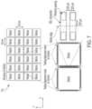
- FIG. 1shows a semiconductor device 50 that includes a wafer 51 .
- At least two reticle areas 52are disposed within wafer 51 , where some or all the reticle areas have a plurality of circuitry of a same design.
- Circuitry within each reticle areas 52includes at least one well circuit 53 and a routing circuit 54 .
- the routing circuit 54routes a signal of a first type 55 from a first side 61 of the reticle area 52 towards a second side 62 of the reticle area 52 along a first direction y, and routes a signal of a second type 56 from a third side of the reticle area 63 towards a fourth side of the reticle area 64 along a second direction x.
- Semiconductor device 50is configured to be used with a biochemical sensor that comprises a multiple-well array.
- semiconductor device 50may be coupled to a multiple-well array 1 along the z-direction, such that well circuit 53 in respective reticle area 52 is in electrical communication with a respective well 2 in the multiple-well array 1 .
- the routing circuit 54may include one or more shift registers 72 .
- a 96-well plate 10is provided as part of a biosensor for assessment of biological specimens such as single cells disposed within the arrays of wells 12 .
- the well 12may have an array of electrodes 14 disposed in the well, for example at a bottom surface of a well 12 , to serve as probes that can interface extracellularly or intracellularly with a specimen in the well.
- the 96-well plate 10is attached to a semiconductor device 100 that includes a substrate 110 and an interposer 102 .
- substrate 110comprises an integrated circuit (IC), and is bonded to an interposer printed circuit board (PCB) via wire-bonding or flip-chip solder bump connection.
- ICintegrated circuit
- PCBinterposer printed circuit board
- Circuitry within substrate 110is situated below each well 12 and are in electrical communication with electrodes 14 disposed in the wells 12 .
- plate 10is shown as a 96-well array for illustration purposes only, and other aspects of the present disclosure are not so limited, and can be applicable, for example, to 24-well, 384-well, or other suitable multiple-well array formats known in the field.
- FIG. 2 Ais a high level schematic diagram illustrating an exemplary CMOS-Multiwell Platform, in accordance with some embodiments.
- a 96-well plate 10is provided as part of a biosensor for assessment of biological specimens such as single cells disposed within the arrays of wells 12 .
- the well 12may have an array of electrodes 14 disposed in the well, for example at a bottom surface of a well 12 , to serve as probes that can interface extracellularly or intracellularly with a specimen in the well.
- the 96-well plate 10is attached to a semiconductor device 100 that includes a substrate 110 and an interposer 102 .
- substrate 110comprises an integrated circuit (IC), and is bonded to an interposer printed circuit board (PCB) via wire-bonding. Circuitry within substrate 110 is situated below each well 12 and are in electrical communication with electrodes 14 disposed in the wells 12 . It should be appreciated that plate 10 is shown as a 96-well array for illustration purposes only, and other aspects of the present disclosure are not so limited, and can be applicable, for example, to 24-well, 384-well, or other suitable multiple-well array formats known in the field.
- the number of electrodes in electrode array 14may be at least 1000, at least 4000, or in some embodiments at least 1 million, as aspects of the present disclosure is not so limited. It should be appreciated that while the electrode array 14 are shown disposed within wells 12 of plate 10 , it is not necessary for electrode array 14 to be provided as part of the multiple-well plate, or as a separate component from the semiconductor device 100 . In some embodiments, electrode array 14 may be disposed within semiconductor device 100 , for example as conductors exposed from an insulative surface of substrate 110 that faces plate 10 . In some embodiments, electrode array 14 may be patterned on a surface of substrate 110 as part of the semiconductor fabrication process to form semiconductor device 100 , and may be metal pads that comprise Au or Pt, or alloys thereof. In such embodiments, substrate 110 may additionally comprise conductors that interconnect vertically the exposed electrode array 14 to circuitry within substrate 110 .
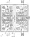
- FIG. 2 Bis a top view schematic diagram of an exemplary semiconductor device 200 that can be used in a CMOS-Multiwell Platform, in accordance with some embodiments.
- the substrate 210may be referred to as a multiwell IC.
- Substrate 210may be a Si wafer, and each reticle area may be of an identical design that is fabricated by stepping the reticle of a standard lithography process along the X- and Y-directions without the need to dice the wafer.
- Each reticle areamay comprise multiple layers, including an active layer that comprises silicon components, as well as one or more layers comprising conductors and dielectric materials as connections and interconnections.
- Each reticle areamay contain one or more identical well circuits 230 , as shown in the magnified view image in FIG. 2 C .
- each reticle area 220may be a CMOS chip and all 96 chips are connected through cross-reticle connections that can be fabricated using standard semiconductor processing techniques.
- FIG. 3is a schematic block diagram illustrating an exemplary apparatus 1000 for electrical assessment of a biological specimen, in accordance with some embodiments.
- the apparatus 1000may be an example of a CMOS-Multiwell Platform, and includes a plate 30 having a multiple-well array.
- the plate 30may be a standard 24-, 96- or 384-well plate in some non-limiting examples.
- the plate 30is attached mechanically to a wafer 310 , which may be a multiwell IC.
- Wafer 310may be a silicon wafer that comprise a plurality of reticle areas 320 .
- Reticle areas 320may be arranged in an array on a surface of wafer 310 , and may be un-diced silicon dies.
- Adjacent reticle areasare in electrical communications with each other, for example via cross-reticle connections.
- Each reticle areamay have an identical circuit design.
- each reticle areamay have N identical well circuits 330 .
- one well circuitis provided to electrically interface with electrodes in one well of the plate 30 .
- Nmay be 1 for 24-well format, 4 for 96-well format and 16 for 384-well format.
- the design of the reticles and well circuitsis not limited to providing a one-to-one correspondence with the wells, and more or less than one well circuit may be provided to a well.
- the well circuitsmay be reconfigured, for example by using a plurality of switches, to couple to different wells.
- wafer 310is attached to an interposer 302 both mechanically, and electrically.
- Any suitable bonding method known in the field of semiconductor packagingmay be used to couple wafer 310 with interposer 302 , such as but not limited to flip-chip bonding or wire-bonding.
- Apparatus 1000may additionally and optionally include components for carrying out electrical assessment of a biological specimen disposed in the wells of plate 30 .
- Such componentsmay include a data acquisition system in communication with contact pads on interposer 302 , one or more computers having processors that can execute programs stored in one or more storage medium to implement a method of carrying out testing using the wafer 310 .
- roboticsmay be used in connection with plate 30 to provide automatic sample handling and placement.
- FIG. 4is a cross-section view schematic diagram of an exemplary apparatus, in accordance with some embodiments.
- a first surface or top surface 422 of the multiwell IC 420is facing the wells 42 in the plate 40
- a second or bottom surface 424 of the multiwell ICis facing opposite the wells, and faces the interposer.
- a plurality of reticle areas(not shown) are disposed in the top surface of the multiwell IC.
- Multiwell IC 420is coupled to interposer 402 at a wafer attach surface 406 .
- the interposer 402may comprise a cavity 404 as shown in FIG. 4 , which in some examples may have a cavity height that is similar to the thickness of the wafer that forms multiwell IC 420 .
- Wafer attach surface 406may be disposed at the bottom surface of cavity 404 , and the multiwell IC 420 is positioned inside the cavity 404 and wire-bonded to the interposer 402 .
- the input/output (I/O) of the multiwell IC 420may be wire-bonded and routed to the contact pads 408 disposed on a mounting surface 409 at the bottom of the interposer 402 .
- connection between the interposer and multiwell ICis not limited to wire-bonding as shown in the example in FIG. 4 , and in some embodiments may be done via flip-chip bonding, or other techniques.
- Pads 408may alternatively be implemented as gold fingers, cables, or connectors (e.g. USB) instead of contact pads.
- a PCB with center opening and having pads aligned with the pads of a multiwell ICcan be used for flip-chip bonding, where a solder bump will connect the interposer pads with the array of pads in the multiwell IC directly without wire-bonding.
- wells 42are open bottom wells that are attached onto the multiwell IC 420 and the interposer 402 , such that the interior of wells 42 may be fluidically connected to the top surface 422 of multiwell IC 420 , although aspects of the present disclosure are not limited to open bottom wells.
- FIG. 5is a cross-section view schematic diagram of an exemplary apparatus that could interface with an external data acquisition system, in accordance with some embodiments.
- an environment chamber or incubator 506 with key slot featureis used to guide the well-plate 40 to align with an array of spring-loaded contacts 504 on a second substrate 502 with matching pattern to the contact pads 408 on the interposer 402 .
- the enclosed chamber 506provides an isolated environment for the experiment wells 42 with gas control.
- second substrate 502may provide mechanical support and environmental sealing for chamber 506 .
- second substrate 502may provide electrical interconnections between the multiwell IC 420 within chamber 506 to an external data acquisition system outside of chamber 506 .
- Second substrate 502may be physically secured to interposer 402 by a suitable clamping technique.
- second substrate 502is coupled to interposer 402 via a magnetic force, for example using a pair of magnets disposed on the mounting surface 409 of interposer 402 and a top surface of second substrate 502 , which provides a pulling/snapping force to ensure sufficient contact between the pads 408 and spring-loaded contacts 504 .
- FIG. 6is a plan-view schematic diagram of an exemplary environment chamber 606 , in accordance with some embodiments.
- FIG. 6shows that environment chamber 606 comprises a lid 608 that can snap on to a housing 610 to create an enclosure that has two openings towards the bottom, with opening 602 open to a well-plate, and opening 604 for providing gas control to the environment chamber 606 .
- FIG. 7is a top view schematic diagram illustrating an exemplary wafer 710 , in accordance with some embodiments.
- the reticle areamay be designed in a specific symmetry so that a simple redistribution layer (RDL) connections between the IO pads of neighbor reticle areas will allow I/O signals to pass through the entire wafer.
- the RDLmay comprise conductors such as metal traces that serve as cross-reticle connections interconnect adjacent reticle areas, IO pads disposed around the periphery of wafer 710 may be then wire-bonded to the interposer as shown in FIG. 4 .
- FIG. 8is a top view schematic diagram illustrating an example circuit design within a reticle area, in accordance with some embodiments.
- a reticle areacontains 4 identical well circuits 830 positioned to allow standard well-plate alignment (e.g. 9 mm distance), although it should be appreciated that variations of the design as shown in FIG. 8 having any suitable number of well circuits may be used for other multiple-well arrays such as 24-well and 384-well plates.
- the 24-well version reticleonly one well circuit should be centered at the reticle in this example.
- 16 well circuitsmay be positioned to allow standard 4.5 mm well distance.
- reticle area 820is designed to have left-right and top-bottom symmetric IO pads on the periphery so that signal can be routed cross the reticle area and pass into adjacent reticle areas through the cross-reticle signal buses 820 .
- Each well circuit 830 inside the reticle area 820may have dedicated signal buffers to buffer the global signal to local well circuit and vice versa.
- different types of signalsare routed along the X- and Y-directions, to increase routing efficiency when daisy-chaining a plurality of rows and columns of reticle areas.
- the cross-reticle signal busses 822may be a routing circuit that routes digital signal along the X-direction from the left side of the reticle area towards the right side, and routes analog signals along the Y-direction from the top side of the reticle area towards the bottom side.
- FIG. 9is a schematic block diagram illustrating an exemplary well circuit 930 inside a reticle area 920 , in accordance with some embodiments.
- a well circuit 930a plurality of peripheral circuits 934 are designed to be able to connect to all or a subset of an array of electrodes 936 within a well of a multiple-well array attached atop the wafer that the reticle area 920 is disposed in.
- the array of electrodesmay also be referred to as pixels, each pixel occupying a pixel area.
- well circuit 930has 256 peripheral circuits.
- all or a subset of the peripheral circuitsare able to connect to all or a subset of 4096 pixels in a well to allow high density (HD), medium density (MD) or low density (LD) connections.
- Any set of arbitrary pixelscan also act as reference electrode by connection the electrode to the reference electrode bias (V REF )
- V REFreference electrode bias
- a subset of 16 ⁇ 16 (32 ⁇ 32) pixelsare recorded out of the total 64 ⁇ 64 available pixels. This routing design allows scanning of the recording area (16 ⁇ 16 for HD and 32 ⁇ 32 for MD) across the entire available active area (64 ⁇ 64). This example design allows customized experiment setups from well to well.
- switches 932may also selectively couple the peripheral circuits 934 to one or more optoelectronic components instead of an electrode.
- the optoelectronic componentinclude photodetectors or photoemitters such as light-emitting diodes, such that the functionality for each well above a reticle area can be individually and independently programmed to allow a range of different assessments to be performed within the multiple-well array.
- the optoelectronic componentmay be a photodiode fabricated on the wafer such as wafer 710 , and disposed in an optoelectronic sensing region within a pixel area.
- a lateral spatial span of the optoelectronic sensing regioncovers the same area as the electrode array in the pixel area, although it should be appreciated that other suitable placement or dimension for the optoelectronic component may be used.
- the optoelectronic interfacehas a 1:1 mapping with the electrical interface, and an optoelectronic component is provided for each electrode array or each pixel area, although the 1:1 mapping is not a requirement.
- the peripheral circuit 934may each include a stimulation circuit and a recording circuit.
- the stimulation circuitmay comprise one or more current injectors.
- Some aspects of the peripheral circuit designare related to current-based stimulators for electrogenic cells and related methods, as disclosed in International Application Publication. No. WO 2019/010343, the disclosure of which is hereby incorporated by reference in its entirety. Some aspects may also be related to electronic circuits for analyzing electrogenic cells and related methods, as disclosed in International Application Publication. No. WO 2019/089495, the disclosure of which is hereby incorporated by reference in its entirety.
- global digital control and configuration signalsmay be routed from left to right in the center of the reticle, whereas global analog signals (output and control signals) are routed from top to bottom, also in the center of the reticle as shown in see FIG. 8 .
- each well circuitbuffers in and out its local signals to the global buses.
- SPISerial-Peripheral-Interface
- the highest-level SPIselect one or more specific well(s) from the multiwell IC to be programed in the lower level two SPIs.
- the input (D IN ) of this SPImay come from an I/O pad on the left side of a reticle area, and the output (D OUT ) of this SPI is routed to the symmetric I/O pad on the right side of the reticle area, which allows simple RDL connections to daisy-chain the reticles together.
- the lower two level SPIsmay have shared control signals across the entire multiwell IC.
- the Address Select SPIselect the components (e.g. peripheral circuits and temperature control) within the well circuit to be programed by the Configuration SPI, which write the registers of the selected components in the selected wells.
- each reticle areamay have, for example, 8 analog output buses routed from top I/O pads to bottom I/O pads.
- the analog output of the peripheral circuits in each wellis multiplexed into one of the eight buses. Since each reticle has 4 wells but 8 analog buses, this design allows the top two rows (2 ⁇ 6) of reticle areas to be read out from the top side and the bottom two rows (also 2 ⁇ 6) to be read out from the bottom side of the reticle area, although aspects of the present disclosure are not so limited and other suitable readout schemes may be used.
- the inventorshave recognized and appreciated that the routing of analog and digital signals as described herein may advantageously improve signal routing efficiency by simplifying the routing design.
- signalscan be routed all digitally, after analog signals are converted in analog-to-digital converters within the reticle, and converted back to analog form using digital-to-analog converters when needed to provide stimulation.
- FIGS. 10 A and 10 Bare top view and bottom view schematic diagrams, respectively, of an example design of an environment chamber lid with reference electrodes, in accordance with some embodiments.
- the lidmay include Ag/AgCl reference electrode, which the inventors have recognized as an importance reference electrode material in electrochemical applications.
- 24/96/384 reference electrodes and their control circuitsare integrated on a PCB Lid with the same form factor as the standard well-plate.
- the control circuitsmay be programed with SPI so that customized experiments can be perform from well to well.
- the reference electrodescan measure solution/media voltage/current and apply stimulation to the experiment well.
- the lid designcan additionally be used to accommodate a photodiode or a photoemitter lid for optical applications (e.g. optogenetic/optical electrochemical sensing).
- FIGS. 11 A, 11 B and 11 Cillustrate several exemplary applications of the apparatus as disclosed herein.
- a CMOS-Multiwell platform as described hereincan also leverage impedance and electrochemical measurement to extend the area of applications.
- a CMOS-Multiwell platformmay be used for cell or tissue mapping, such as spatial characterization of one or more characteristics of cells or tissues disposed on a surface of a well. Such characteristics may be related to one or more phenomena such as cell confluency, cell migration, cell viability/toxicity, and cell adhesion.
- an impedance map between electrodes in the electrode arraymay be created that is representative of spatial distribution of cells relative to the electrodes.
- the CMOS-Multiwell platform as described hereinmay be used for performing patterned redox electrochemistry in selected spatial areas by selectively activating a select pattern of electrodes within a well.
- the patterned electrochemistrymay be used to interact with a pattern of cells electrochemically, or to perform electrochemical sensing such as sensing of pH, O 2 level, etc. in selectively patterned spatial areas.
- the CMOS-Multiwell platformmay be used for single-cell measurements, including but not limited to single-cell action potential or ion-channel measurements.
- the single-cell measurementsmay also include network measurements to characterize conduction velocity for cardiac cells, or synapse mapping of neurons in some non-limiting examples.
- the inventionmay be embodied as a method, of which an example has been provided.
- the acts performed as part of the methodmay be ordered in any suitable way. Accordingly, embodiments may be constructed in which acts are performed in an order different than illustrated, which may include performing some acts simultaneously, even though shown as sequential acts in illustrative embodiments.
- the terms “approximately” and “about”may be used to mean within ⁇ 20% of a target value in some embodiments, within ⁇ 10% of a target value in some embodiments, within ⁇ 5% of a target value in some embodiments, and yet within ⁇ 2% of a target value in some embodiments.
- the terms “approximately” and “about”may include the target value.
Landscapes
- Health & Medical Sciences (AREA)
- Engineering & Computer Science (AREA)
- Life Sciences & Earth Sciences (AREA)
- Biomedical Technology (AREA)
- Chemical & Material Sciences (AREA)
- Physics & Mathematics (AREA)
- General Health & Medical Sciences (AREA)
- Hematology (AREA)
- Analytical Chemistry (AREA)
- Food Science & Technology (AREA)
- Immunology (AREA)
- Medicinal Chemistry (AREA)
- Molecular Biology (AREA)
- Biochemistry (AREA)
- Biophysics (AREA)
- General Physics & Mathematics (AREA)
- Urology & Nephrology (AREA)
- Pathology (AREA)
- Clinical Laboratory Science (AREA)
- Chemical Kinetics & Catalysis (AREA)
- Optics & Photonics (AREA)
- Apparatus Associated With Microorganisms And Enzymes (AREA)
- Testing Or Measuring Of Semiconductors Or The Like (AREA)
Abstract
Description
Claims (24)
Priority Applications (1)
| Application Number | Priority Date | Filing Date | Title |
|---|---|---|---|
| US17/891,964US12265076B2 (en) | 2020-06-17 | 2022-08-19 | Complementary metal-oxide-semiconductor (CMOS) multi-well apparatus for electrical cell assessment |
Applications Claiming Priority (3)
| Application Number | Priority Date | Filing Date | Title |
|---|---|---|---|
| US202063040412P | 2020-06-17 | 2020-06-17 | |
| PCT/US2021/037604WO2021257686A1 (en) | 2020-06-17 | 2021-06-16 | Complementary metal-oxide-semiconductor (cmos) multi-well apparatus for electrical cell assessment |
| US17/891,964US12265076B2 (en) | 2020-06-17 | 2022-08-19 | Complementary metal-oxide-semiconductor (CMOS) multi-well apparatus for electrical cell assessment |
Related Parent Applications (1)
| Application Number | Title | Priority Date | Filing Date |
|---|---|---|---|
| PCT/US2021/037604ContinuationWO2021257686A1 (en) | 2020-06-17 | 2021-06-16 | Complementary metal-oxide-semiconductor (cmos) multi-well apparatus for electrical cell assessment |
Publications (2)
| Publication Number | Publication Date |
|---|---|
| US20230184739A1 US20230184739A1 (en) | 2023-06-15 |
| US12265076B2true US12265076B2 (en) | 2025-04-01 |
Family
ID=79268347
Family Applications (1)
| Application Number | Title | Priority Date | Filing Date |
|---|---|---|---|
| US17/891,964ActiveUS12265076B2 (en) | 2020-06-17 | 2022-08-19 | Complementary metal-oxide-semiconductor (CMOS) multi-well apparatus for electrical cell assessment |
Country Status (7)
| Country | Link |
|---|---|
| US (1) | US12265076B2 (en) |
| EP (1) | EP4168316A4 (en) |
| JP (1) | JP2023531909A (en) |
| CN (1) | CN116075722A (en) |
| CA (1) | CA3187266A1 (en) |
| IL (1) | IL299095A (en) |
| WO (1) | WO2021257686A1 (en) |
Cited By (1)
| Publication number | Priority date | Publication date | Assignee | Title |
|---|---|---|---|---|
| US12405242B2 (en) | 2020-06-17 | 2025-09-02 | President And Fellows Of Harvard College | Systems and methods for patterning and spatial electrochemical mapping of cells |
Families Citing this family (7)
| Publication number | Priority date | Publication date | Assignee | Title |
|---|---|---|---|---|
| WO2016112315A2 (en) | 2015-01-09 | 2016-07-14 | President And Fellows Of Harvard College | Nanowire arrays for neurotechnology and other applications |
| WO2019010343A1 (en) | 2017-07-07 | 2019-01-10 | President And Fellows Of Harvard College | Current-based stimulators for electrogenic cells and related methods |
| US12174140B2 (en) | 2017-11-01 | 2024-12-24 | President And Fellows Of Harvard College | Electronic circuits for analyzing electrogenic cells and related methods |
| IL299096A (en) | 2020-06-17 | 2023-02-01 | Harvard College | Apparatuses for cell mapping via impedance measurements and methods to operate the same |
| EP4168316A4 (en) | 2020-06-17 | 2024-07-10 | President and Fellows of Harvard College | Complementary metal-oxide-semiconductor (cmos) multi-well apparatus for electrical cell assessment |
| TWI825609B (en)* | 2021-10-14 | 2023-12-11 | 大陸商廣州印芯半導體技術有限公司 | Biomolecular image sensor and method thereof for detecting biological molecules |
| WO2024238994A1 (en)* | 2023-05-18 | 2024-11-21 | CytoTronics | Semiconductor-based measurement devices |
Citations (76)
| Publication number | Priority date | Publication date | Assignee | Title |
|---|---|---|---|---|
| US5072194A (en) | 1989-08-25 | 1991-12-10 | U.S. Philips Corporation | Differential amplifier with capacitive coupling |
| US5233985A (en) | 1990-08-10 | 1993-08-10 | Medtronic, Inc. | Cardiac pacemaker with operational amplifier output circuit |
| US5605612A (en) | 1993-11-11 | 1997-02-25 | Goldstar Electron Co., Ltd. | Gas sensor and manufacturing method of the same |
| DE19529371C2 (en) | 1995-08-10 | 1998-01-22 | Nmi Univ Tuebingen | Microelectrode arrangement |
| US20020010415A1 (en) | 2000-05-22 | 2002-01-24 | Simon Adam J. | System and method for assessing the performance of a pharmaceutical agent delivery system |
| US20020045318A1 (en) | 1999-04-09 | 2002-04-18 | Coming Chen | Method for manufacturing mos transistor |
| US20020182591A1 (en) | 2001-06-05 | 2002-12-05 | Applied Biophysics, Inc. | Electrical wounding assay for cells in vitro |
| US20020190732A1 (en) | 2000-03-15 | 2002-12-19 | Jing Cheng | Apparatus and method for high throughput electrorotation analysis |
| EP1271144A1 (en) | 2001-06-27 | 2003-01-02 | flyion GmbH | Method and circuitry for controlling and measuring electrical parameters in a biological membrane |
| US20030100189A1 (en) | 2001-11-28 | 2003-05-29 | Chun-Tao Lee | Method for increasing the capacity of an integrated circuit device |
| US20040100290A1 (en) | 1998-12-22 | 2004-05-27 | John Pope | Method of using an array of electrodes for high throughput development and testing of materials |
| US20050170510A1 (en) | 2003-12-08 | 2005-08-04 | Yong Huang | Device and method for controlled electroporation and molecular delivery into cells and tissue |
| US20050253137A1 (en) | 2003-11-20 | 2005-11-17 | President And Fellows Of Harvard College | Nanoscale arrays, robust nanostructures, and related devices |
| US20050282284A1 (en) | 1999-07-21 | 2005-12-22 | The Regents Of The University Of California | Controlled electroporation and mass transfer across cell membranes in tissue |
| US20060121446A1 (en) | 2002-12-20 | 2006-06-08 | Abassi Yama A | Device and method for electroporation-based delivery of molecules into cells and dynamic monitoring of cell responses |
| US20070043301A1 (en) | 2002-05-14 | 2007-02-22 | Idex Asa | Volume specific characterization of human skin by electrical immitance |
| US20070072257A1 (en) | 2004-03-31 | 2007-03-29 | Negulescu Paul A | Multiwell plate assembly for use in high throughput assays |
| US20070087401A1 (en) | 2003-10-17 | 2007-04-19 | Andy Neilson | Analysis of metabolic activity in cells using extracellular flux rate measurements |
| US20070187840A1 (en) | 2005-11-21 | 2007-08-16 | Dell Acqua-Bellavitis Ludovico | Nanoscale probes for electrophysiological applications |
| US20070264634A1 (en) | 2002-10-10 | 2007-11-15 | Nanosys, Inc. | Nano-chem-fet based biosensors |
| US20080009434A1 (en) | 2004-09-08 | 2008-01-10 | Meital Reches | Peptide Nanostructures Containing End-Capping Modified Peptides And Methods Of Generating And Using The Same |
| US20080218939A1 (en) | 2007-03-09 | 2008-09-11 | Marcus Matthew S | Nanowire supercapacitor electrode |
| JP2008269725A (en) | 2007-04-23 | 2008-11-06 | Sharp Corp | Electrical characteristic evaluation equipment |
| US20090146735A1 (en) | 2007-12-11 | 2009-06-11 | Samsung Electro-Mechanics Co., Ltd. | Switched capacitor resonator and sigma-delta modulator using the same |
| US20090205201A1 (en) | 2002-12-20 | 2009-08-20 | Acea Biosciences, Inc. | Impedance Based Devices and Methods for Use in Assays |
| US20090227066A1 (en) | 2008-03-06 | 2009-09-10 | International Business Machines Corporation | Method of forming ring electrode |
| US20090255801A1 (en) | 2008-04-11 | 2009-10-15 | Haas Alfred M | Programmable Electrode Arrays and Methods for Manipulating and Sensing Cells and Substances Using Same |
| WO2009137440A1 (en) | 2008-05-05 | 2009-11-12 | Acea Biosciences, Inc. | Label-free monitoring of excitation-contraction coupling and excitable cells using impedance based systems with millisecond time resolution |
| US20100164110A1 (en) | 2006-08-17 | 2010-07-01 | Song Jin | Metal silicide nanowires and methods for their production |
| US20100304425A1 (en) | 2009-05-26 | 2010-12-02 | Speller Sylvia | Method for the ex vivo analysis of a cell and apparatus therefore |
| US20110210718A1 (en) | 2010-02-26 | 2011-09-01 | Dionex Corporation | Analytic Device With PhotoVoltaic Power Source |
| US20110233512A1 (en) | 2005-08-16 | 2011-09-29 | The Regents Of The University Of California | Vertical integrated silicon nanowire field effect transistors and methods of fabrication |
| US20110253982A1 (en) | 2008-10-28 | 2011-10-20 | The Regents Of The University Of California | Vertical group iii-v nanowires on si, heterostructures, flexible arrays and fabrication |
| US8159300B2 (en) | 2007-06-27 | 2012-04-17 | Thine Electronics, Inc. | Signal conversion circuit and rail-to-rail circuit |
| WO2012050881A2 (en) | 2010-09-29 | 2012-04-19 | President And Fellows Of Harvard College | Molecular delivery with nanowires |
| WO2012050876A2 (en) | 2010-09-29 | 2012-04-19 | President And Fellows Of Harvard College | Nanowires for electrophysiological applications |
| US20120094328A1 (en) | 2009-06-25 | 2012-04-19 | Kirin Holdings Kabushkik Kaisha | Fermentation product of cereal plant-derived material and immunomodulator |
| US20120157804A1 (en) | 2009-12-16 | 2012-06-21 | Rogers John A | High-Speed, High-Resolution Electrophysiology In-Vivo Using Conformal Electronics |
| US20120182168A1 (en) | 2011-01-19 | 2012-07-19 | Analog Devices, Inc. | Active rc resonators with enhanced q factor |
| US8227223B2 (en) | 2009-01-27 | 2012-07-24 | Applied Biophysics, Inc. | Method and apparatus for facilitating evaluating migration of cells in vitro |
| US20130041282A1 (en) | 2010-04-28 | 2013-02-14 | M.I.Tech Co., Ltd. | Apparatus for measuring interfacial impedance between the body and a stimulating electrode |
| US20130041235A1 (en) | 2009-12-16 | 2013-02-14 | John A. Rogers | Flexible and Stretchable Electronic Systems for Epidermal Electronics |
| US20130072775A1 (en) | 2011-06-03 | 2013-03-21 | John Rogers | Conformable Actively Multiplexed High-Density Surface Electrode Array for Brain Interfacing |
| US20130115705A1 (en) | 2010-06-08 | 2013-05-09 | Ramot At Tel-Aviv University Ltd. | Functionalized nanostructures for detecting nitro-containing compounds |
| US20130123136A1 (en) | 2002-12-20 | 2013-05-16 | Acea Biosciences, Inc | Real-time electronic cell sensing system and applications for cytotoxicity profiling and compound assays |
| US20130338746A1 (en) | 2012-06-18 | 2013-12-19 | Georgia Institute Of Technology | 3d microelectrode device for live tissue applications |
| US20130341734A1 (en)* | 2012-06-21 | 2013-12-26 | Nxp B.V. | Integrated circuit with sensors and manufacturing method |
| US20140001041A1 (en) | 2010-11-08 | 2014-01-02 | Agency For Science, Technology And Research | Biosensor |
| US20150005680A1 (en) | 2011-02-23 | 2015-01-01 | John D. LIPANI | System and Methods for Diagnosis and Treatment of Discogenic Lower Back Pain |
| WO2015012955A1 (en) | 2013-07-26 | 2015-01-29 | Axion BioSystems | Devices, systems and methods for high-throughput electrophysiology |
| US20150148863A1 (en) | 2013-11-25 | 2015-05-28 | Ybrain Inc. | Brain stimulating system |
| US9121806B1 (en) | 2007-07-26 | 2015-09-01 | University Of South Florida | Impedance spectroscopy-based cellular analysis device |
| US20150377856A1 (en) | 2011-07-20 | 2015-12-31 | The Regents Of The University Of California | Compensated patch-clamp amplifier for nanopore polynucleotide sequencing and other applications |
| US20150376811A1 (en) | 2011-02-22 | 2015-12-31 | Massachusetts Institute Of Technology | Electrophoretic-deposited surfaces |
| US20160047770A1 (en) | 2014-08-12 | 2016-02-18 | Axion Biosystems, Inc. | Cell-based biosensor array and associated methods for manufacturing the same |
| US20160096173A1 (en) | 2003-09-10 | 2016-04-07 | Seahorse Bioscience | Method and device for measuring multiple physiological properties of cells |
| US9360469B1 (en) | 2014-06-12 | 2016-06-07 | Axion Biosystems, Inc. | Multiwell microelectrode array with optical stimulation |
| WO2016112315A2 (en) | 2015-01-09 | 2016-07-14 | President And Fellows Of Harvard College | Nanowire arrays for neurotechnology and other applications |
| US20160245790A1 (en) | 2013-08-27 | 2016-08-25 | Osaka University | Device for thermally denaturing biomolecule and method for producing device |
| US20160245788A1 (en) | 2015-02-20 | 2016-08-25 | Georgia Tech Research Corporation | Multimodality cmos sensor array for physiological characterization of cells |
| US20160278713A1 (en) | 2015-03-25 | 2016-09-29 | Ecole Polytechnique Federale De Lausanne (Epfl) | Compact low-power recording architecture for multichannel acquisition of biological signals and method for compressing said biological signal data |
| US20170058246A1 (en) | 2015-08-28 | 2017-03-02 | Axion Biosystems, Inc. | Device and system for creating and maintaining a localized environment for a cell culture plate |
| US20170176414A1 (en) | 2016-03-03 | 2017-06-22 | Mohammad Abdolahad | Electrochemical method and device for detecting the effect of anticancer drugs |
| US9700221B2 (en) | 2013-03-06 | 2017-07-11 | Axion Biosystems, Inc. | Non-invasive segmentable three-dimensional microelectrode array patch for neurophysiological diagnostics and therapeutic stimulation |
| US20170336384A1 (en) | 2016-05-20 | 2017-11-23 | Tohoku University | Electrochemical imaging method, electrochemical measurement apparatus and transducer |
| US9983198B2 (en) | 2015-03-19 | 2018-05-29 | Axion Biosystems, Inc. | Systems and methods for assessing data collected from an electrically active cell culture |
| US20180163165A1 (en) | 2013-11-05 | 2018-06-14 | Axion Biosystems, Inc. | Devices, systems, and methods for targeted plating of materials in high-throughput culture plates |
| US20180246079A1 (en) | 2015-11-20 | 2018-08-30 | Acea Biosciences, Inc. | Cell-substrate impedance monitoring of cancer cells |
| WO2019010343A1 (en) | 2017-07-07 | 2019-01-10 | President And Fellows Of Harvard College | Current-based stimulators for electrogenic cells and related methods |
| WO2019089495A1 (en) | 2017-11-01 | 2019-05-09 | President And Fellows Of Harvard College | Electronic circuits for analyzing electrogenic cells and related methods |
| US20200064336A1 (en) | 2018-08-21 | 2020-02-27 | International Business Machines Corporation | Well Plate Cover With Embedded Electronic Sensors For Monitoring Cell Metabolism |
| US20210236033A1 (en) | 2014-02-01 | 2021-08-05 | Biocircuit Technologies, Inc. | Neural interfacing device |
| US11167131B2 (en) | 2016-09-06 | 2021-11-09 | Biocircuit Technologies, Inc. | Devices and methods for repairing damage to a tissue |
| WO2021257705A1 (en) | 2020-06-17 | 2021-12-23 | President And Fellows Of Harvard College | Systems and methods for patterning and spatial electrochemical mapping of cells |
| WO2021257686A1 (en) | 2020-06-17 | 2021-12-23 | President And Fellows Of Harvard College | Complementary metal-oxide-semiconductor (cmos) multi-well apparatus for electrical cell assessment |
| WO2021257701A1 (en) | 2020-06-17 | 2021-12-23 | President And Fellows Of Harvard College | Apparatuses for cell mapping via impedance measurements and methods to operate the same |
Family Cites Families (1)
| Publication number | Priority date | Publication date | Assignee | Title |
|---|---|---|---|---|
| CN111164411A (en)* | 2017-08-17 | 2020-05-15 | 雅培医护站股份有限公司 | Method of imaging assay beads in a biological sample |
- 2021
- 2021-06-16EPEP21825487.8Apatent/EP4168316A4/enactivePending
- 2021-06-16JPJP2022577744Apatent/JP2023531909A/enactivePending
- 2021-06-16WOPCT/US2021/037604patent/WO2021257686A1/ennot_activeCeased
- 2021-06-16CNCN202180058447.2Apatent/CN116075722A/enactivePending
- 2021-06-16ILIL299095Apatent/IL299095A/enunknown
- 2021-06-16CACA3187266Apatent/CA3187266A1/enactivePending
- 2022
- 2022-08-19USUS17/891,964patent/US12265076B2/enactiveActive
Patent Citations (95)
| Publication number | Priority date | Publication date | Assignee | Title |
|---|---|---|---|---|
| US5072194A (en) | 1989-08-25 | 1991-12-10 | U.S. Philips Corporation | Differential amplifier with capacitive coupling |
| US5233985A (en) | 1990-08-10 | 1993-08-10 | Medtronic, Inc. | Cardiac pacemaker with operational amplifier output circuit |
| US5605612A (en) | 1993-11-11 | 1997-02-25 | Goldstar Electron Co., Ltd. | Gas sensor and manufacturing method of the same |
| DE19529371C2 (en) | 1995-08-10 | 1998-01-22 | Nmi Univ Tuebingen | Microelectrode arrangement |
| US6032062A (en) | 1995-08-10 | 2000-02-29 | Nmi Naturwissenschaftliches Und Medizinisches Institut | Microelectrode arrangement |
| US20040100290A1 (en) | 1998-12-22 | 2004-05-27 | John Pope | Method of using an array of electrodes for high throughput development and testing of materials |
| US20020045318A1 (en) | 1999-04-09 | 2002-04-18 | Coming Chen | Method for manufacturing mos transistor |
| US20050282284A1 (en) | 1999-07-21 | 2005-12-22 | The Regents Of The University Of California | Controlled electroporation and mass transfer across cell membranes in tissue |
| US20020190732A1 (en) | 2000-03-15 | 2002-12-19 | Jing Cheng | Apparatus and method for high throughput electrorotation analysis |
| US20020010415A1 (en) | 2000-05-22 | 2002-01-24 | Simon Adam J. | System and method for assessing the performance of a pharmaceutical agent delivery system |
| US7332313B2 (en) | 2001-06-05 | 2008-02-19 | Applied Biophysics, Inc. | Electrical wounding assay for cells in vitro |
| US20020182591A1 (en) | 2001-06-05 | 2002-12-05 | Applied Biophysics, Inc. | Electrical wounding assay for cells in vitro |
| EP1271144A1 (en) | 2001-06-27 | 2003-01-02 | flyion GmbH | Method and circuitry for controlling and measuring electrical parameters in a biological membrane |
| US20030100189A1 (en) | 2001-11-28 | 2003-05-29 | Chun-Tao Lee | Method for increasing the capacity of an integrated circuit device |
| US20070043301A1 (en) | 2002-05-14 | 2007-02-22 | Idex Asa | Volume specific characterization of human skin by electrical immitance |
| US20070264634A1 (en) | 2002-10-10 | 2007-11-15 | Nanosys, Inc. | Nano-chem-fet based biosensors |
| US20090205201A1 (en) | 2002-12-20 | 2009-08-20 | Acea Biosciences, Inc. | Impedance Based Devices and Methods for Use in Assays |
| US20060121446A1 (en) | 2002-12-20 | 2006-06-08 | Abassi Yama A | Device and method for electroporation-based delivery of molecules into cells and dynamic monitoring of cell responses |
| US20140057283A1 (en) | 2002-12-20 | 2014-02-27 | Acea Biosciences, Inc | Impedance based devices and methods for use in assays |
| US20130123136A1 (en) | 2002-12-20 | 2013-05-16 | Acea Biosciences, Inc | Real-time electronic cell sensing system and applications for cytotoxicity profiling and compound assays |
| US20160096173A1 (en) | 2003-09-10 | 2016-04-07 | Seahorse Bioscience | Method and device for measuring multiple physiological properties of cells |
| US20070087401A1 (en) | 2003-10-17 | 2007-04-19 | Andy Neilson | Analysis of metabolic activity in cells using extracellular flux rate measurements |
| US20050253137A1 (en) | 2003-11-20 | 2005-11-17 | President And Fellows Of Harvard College | Nanoscale arrays, robust nanostructures, and related devices |
| US20050170510A1 (en) | 2003-12-08 | 2005-08-04 | Yong Huang | Device and method for controlled electroporation and molecular delivery into cells and tissue |
| US20070072257A1 (en) | 2004-03-31 | 2007-03-29 | Negulescu Paul A | Multiwell plate assembly for use in high throughput assays |
| US20080009434A1 (en) | 2004-09-08 | 2008-01-10 | Meital Reches | Peptide Nanostructures Containing End-Capping Modified Peptides And Methods Of Generating And Using The Same |
| US20110233512A1 (en) | 2005-08-16 | 2011-09-29 | The Regents Of The University Of California | Vertical integrated silicon nanowire field effect transistors and methods of fabrication |
| US20070187840A1 (en) | 2005-11-21 | 2007-08-16 | Dell Acqua-Bellavitis Ludovico | Nanoscale probes for electrophysiological applications |
| US20100164110A1 (en) | 2006-08-17 | 2010-07-01 | Song Jin | Metal silicide nanowires and methods for their production |
| US20080218939A1 (en) | 2007-03-09 | 2008-09-11 | Marcus Matthew S | Nanowire supercapacitor electrode |
| JP2008269725A (en) | 2007-04-23 | 2008-11-06 | Sharp Corp | Electrical characteristic evaluation equipment |
| US8159300B2 (en) | 2007-06-27 | 2012-04-17 | Thine Electronics, Inc. | Signal conversion circuit and rail-to-rail circuit |
| US9121806B1 (en) | 2007-07-26 | 2015-09-01 | University Of South Florida | Impedance spectroscopy-based cellular analysis device |
| US20090146735A1 (en) | 2007-12-11 | 2009-06-11 | Samsung Electro-Mechanics Co., Ltd. | Switched capacitor resonator and sigma-delta modulator using the same |
| US20090227066A1 (en) | 2008-03-06 | 2009-09-10 | International Business Machines Corporation | Method of forming ring electrode |
| US20090255801A1 (en) | 2008-04-11 | 2009-10-15 | Haas Alfred M | Programmable Electrode Arrays and Methods for Manipulating and Sensing Cells and Substances Using Same |
| WO2009137440A1 (en) | 2008-05-05 | 2009-11-12 | Acea Biosciences, Inc. | Label-free monitoring of excitation-contraction coupling and excitable cells using impedance based systems with millisecond time resolution |
| US20110253982A1 (en) | 2008-10-28 | 2011-10-20 | The Regents Of The University Of California | Vertical group iii-v nanowires on si, heterostructures, flexible arrays and fabrication |
| US8227223B2 (en) | 2009-01-27 | 2012-07-24 | Applied Biophysics, Inc. | Method and apparatus for facilitating evaluating migration of cells in vitro |
| US20100304425A1 (en) | 2009-05-26 | 2010-12-02 | Speller Sylvia | Method for the ex vivo analysis of a cell and apparatus therefore |
| US20120094328A1 (en) | 2009-06-25 | 2012-04-19 | Kirin Holdings Kabushkik Kaisha | Fermentation product of cereal plant-derived material and immunomodulator |
| US20120157804A1 (en) | 2009-12-16 | 2012-06-21 | Rogers John A | High-Speed, High-Resolution Electrophysiology In-Vivo Using Conformal Electronics |
| US20130041235A1 (en) | 2009-12-16 | 2013-02-14 | John A. Rogers | Flexible and Stretchable Electronic Systems for Epidermal Electronics |
| US20110210718A1 (en) | 2010-02-26 | 2011-09-01 | Dionex Corporation | Analytic Device With PhotoVoltaic Power Source |
| US20130041282A1 (en) | 2010-04-28 | 2013-02-14 | M.I.Tech Co., Ltd. | Apparatus for measuring interfacial impedance between the body and a stimulating electrode |
| US20130115705A1 (en) | 2010-06-08 | 2013-05-09 | Ramot At Tel-Aviv University Ltd. | Functionalized nanostructures for detecting nitro-containing compounds |
| US20130260467A1 (en) | 2010-09-29 | 2013-10-03 | President And Fellows Of Harvard | Molecular delivery with nanowires |
| WO2012050881A2 (en) | 2010-09-29 | 2012-04-19 | President And Fellows Of Harvard College | Molecular delivery with nanowires |
| WO2012050876A2 (en) | 2010-09-29 | 2012-04-19 | President And Fellows Of Harvard College | Nanowires for electrophysiological applications |
| US20140001041A1 (en) | 2010-11-08 | 2014-01-02 | Agency For Science, Technology And Research | Biosensor |
| US20120182168A1 (en) | 2011-01-19 | 2012-07-19 | Analog Devices, Inc. | Active rc resonators with enhanced q factor |
| US20150376811A1 (en) | 2011-02-22 | 2015-12-31 | Massachusetts Institute Of Technology | Electrophoretic-deposited surfaces |
| US20150005680A1 (en) | 2011-02-23 | 2015-01-01 | John D. LIPANI | System and Methods for Diagnosis and Treatment of Discogenic Lower Back Pain |
| US20130072775A1 (en) | 2011-06-03 | 2013-03-21 | John Rogers | Conformable Actively Multiplexed High-Density Surface Electrode Array for Brain Interfacing |
| US20150377856A1 (en) | 2011-07-20 | 2015-12-31 | The Regents Of The University Of California | Compensated patch-clamp amplifier for nanopore polynucleotide sequencing and other applications |
| US20130338746A1 (en) | 2012-06-18 | 2013-12-19 | Georgia Institute Of Technology | 3d microelectrode device for live tissue applications |
| US20130341734A1 (en)* | 2012-06-21 | 2013-12-26 | Nxp B.V. | Integrated circuit with sensors and manufacturing method |
| US9700221B2 (en) | 2013-03-06 | 2017-07-11 | Axion Biosystems, Inc. | Non-invasive segmentable three-dimensional microelectrode array patch for neurophysiological diagnostics and therapeutic stimulation |
| WO2015012955A1 (en) | 2013-07-26 | 2015-01-29 | Axion BioSystems | Devices, systems and methods for high-throughput electrophysiology |
| US20150027885A1 (en) | 2013-07-26 | 2015-01-29 | Axion BioSystems | Devices, systems and methods for high-throughput electrophysiology |
| JP2016529889A (en) | 2013-07-26 | 2016-09-29 | アクシオン バイオシステムズ, インコーポレイテッド | Devices, systems, and methods for high-throughput electrophysiology |
| US20160245790A1 (en) | 2013-08-27 | 2016-08-25 | Osaka University | Device for thermally denaturing biomolecule and method for producing device |
| US20180163165A1 (en) | 2013-11-05 | 2018-06-14 | Axion Biosystems, Inc. | Devices, systems, and methods for targeted plating of materials in high-throughput culture plates |
| US20150148863A1 (en) | 2013-11-25 | 2015-05-28 | Ybrain Inc. | Brain stimulating system |
| US20210236033A1 (en) | 2014-02-01 | 2021-08-05 | Biocircuit Technologies, Inc. | Neural interfacing device |
| US9360469B1 (en) | 2014-06-12 | 2016-06-07 | Axion Biosystems, Inc. | Multiwell microelectrode array with optical stimulation |
| US20160047770A1 (en) | 2014-08-12 | 2016-02-18 | Axion Biosystems, Inc. | Cell-based biosensor array and associated methods for manufacturing the same |
| WO2016112315A2 (en) | 2015-01-09 | 2016-07-14 | President And Fellows Of Harvard College | Nanowire arrays for neurotechnology and other applications |
| US20180169403A1 (en) | 2015-01-09 | 2018-06-21 | President And Fellows Of Harvard College | Nanowire arrays for neurotechnology and other applications |
| US11833346B2 (en) | 2015-01-09 | 2023-12-05 | President And Fellows Of Harvard College | Integrated circuits for neurotechnology and other applications |
| US20210187280A1 (en) | 2015-01-09 | 2021-06-24 | President And Fellows Of Harvard College | Integrated circuits for neurotechnology and other applications |
| US20160245788A1 (en) | 2015-02-20 | 2016-08-25 | Georgia Tech Research Corporation | Multimodality cmos sensor array for physiological characterization of cells |
| US9983198B2 (en) | 2015-03-19 | 2018-05-29 | Axion Biosystems, Inc. | Systems and methods for assessing data collected from an electrically active cell culture |
| US20160278713A1 (en) | 2015-03-25 | 2016-09-29 | Ecole Polytechnique Federale De Lausanne (Epfl) | Compact low-power recording architecture for multichannel acquisition of biological signals and method for compressing said biological signal data |
| US20170058246A1 (en) | 2015-08-28 | 2017-03-02 | Axion Biosystems, Inc. | Device and system for creating and maintaining a localized environment for a cell culture plate |
| US20180246079A1 (en) | 2015-11-20 | 2018-08-30 | Acea Biosciences, Inc. | Cell-substrate impedance monitoring of cancer cells |
| US20170176414A1 (en) | 2016-03-03 | 2017-06-22 | Mohammad Abdolahad | Electrochemical method and device for detecting the effect of anticancer drugs |
| US20170336384A1 (en) | 2016-05-20 | 2017-11-23 | Tohoku University | Electrochemical imaging method, electrochemical measurement apparatus and transducer |
| US11167131B2 (en) | 2016-09-06 | 2021-11-09 | Biocircuit Technologies, Inc. | Devices and methods for repairing damage to a tissue |
| US20210371846A1 (en) | 2017-07-07 | 2021-12-02 | President And Fellows Of Harvard College | Current-based stimulators for electrogenic cells and related methods |
| US20240219370A1 (en) | 2017-07-07 | 2024-07-04 | President And Fellows Of Harvard College | Current-based stimulators for electrogenic cells and related methods |
| WO2019010343A1 (en) | 2017-07-07 | 2019-01-10 | President And Fellows Of Harvard College | Current-based stimulators for electrogenic cells and related methods |
| US11768196B2 (en) | 2017-07-07 | 2023-09-26 | President And Fellows Of Harvard College | Current-based stimulators for electrogenic cells and related methods |
| US20200292482A1 (en) | 2017-11-01 | 2020-09-17 | President And Fellows Of Harvard College | Electronic circuits for analyzing electrogenic cells and related methods |
| WO2019089495A1 (en) | 2017-11-01 | 2019-05-09 | President And Fellows Of Harvard College | Electronic circuits for analyzing electrogenic cells and related methods |
| US20200064336A1 (en) | 2018-08-21 | 2020-02-27 | International Business Machines Corporation | Well Plate Cover With Embedded Electronic Sensors For Monitoring Cell Metabolism |
| US20220397512A1 (en) | 2020-06-17 | 2022-12-15 | President And Fellows Of Harvard College | Apparatuses for cell mapping via impedance measurements and methods to operate the same |
| US20230014082A1 (en) | 2020-06-17 | 2023-01-19 | President And Fellows Of Harvard College | Systems and methods for patterning and spatial electrochemical mapping of cells |
| US11747321B2 (en) | 2020-06-17 | 2023-09-05 | President And Fellows Of Harvard College | Apparatuses for cell mapping via impedance measurements and methods to operate the same |
| WO2021257701A1 (en) | 2020-06-17 | 2021-12-23 | President And Fellows Of Harvard College | Apparatuses for cell mapping via impedance measurements and methods to operate the same |
| US11774396B2 (en) | 2020-06-17 | 2023-10-03 | President And Fellows Of Harvard College | Systems and methods for patterning and spatial electrochemical mapping of cells |
| WO2021257686A1 (en) | 2020-06-17 | 2021-12-23 | President And Fellows Of Harvard College | Complementary metal-oxide-semiconductor (cmos) multi-well apparatus for electrical cell assessment |
| US20240210380A1 (en) | 2020-06-17 | 2024-06-27 | President And Fellows Of Harvard College | Apparatuses for cell mapping via impedance measurements and methods to operate the same |
| WO2021257705A1 (en) | 2020-06-17 | 2021-12-23 | President And Fellows Of Harvard College | Systems and methods for patterning and spatial electrochemical mapping of cells |
| US20240255461A1 (en) | 2020-06-17 | 2024-08-01 | President And Fellows Of Harvard College | Systems and methods for patterning and spatial electrochemical mapping of cells |
Non-Patent Citations (38)
| Title |
|---|
| Abbott et al., A nanoelectrode array for obtaining intracellular recordings from thousands of connected neurons. Nat Biomed Eng. Feb. 2020;4(2):232-241. doi: 10.1038/s41551-019-0455-7. Epub Sep. 23, 2019. |
| Abbott et al., CMOS nanoelectrode array for all-electrical intracellular electrophysiological imaging. Nat Nanotechnol. May 2017;12(5):460-466 and supplemental information. doi: 10.1038/nnano.2017.3. Epub Feb. 13, 2017. 37 pages. |
| Abbott et al., Multi-parametric functional imaging of cell cultures and tissues with a CMOS microelectrode array. Lab Chip. Mar. 29, 2022;22(7):1286-1296. doi: 10.1039/d1lc00878a. |
| Abbott et al., Optimizing nanoelectrode arrays for scalable intracellular electrophysiology. Accounts of Chem Res. Feb. 13, 2018;51(3):600-608. |
| Crescentini et al., Noise limits of CMOS current interfaces for biosensors: a review. IEEE Trans Biomed Circuits Syst. 2014;8(2):278-292. |
| Extended European Search Report for EP 21825487.8 mailed Jun. 7, 2024. |
| Extended European Search Report mailed May 31, 2024 for Application No. EP 21825407.6 mailed May 31, 2024. |
| Extended European Search Report mailed Sep. 2, 2024 for Application No. EP 21825109.8 mailed Sep. 2, 2024. |
| Giovangrandi et al., Low-cost microelectrode array with integrated heater for extracellular recording of cardiomyocyte cultures using commercial flexible printed circuit technology. Sensors and Actuators B 113. Jan. 17, 2006;113:545-554. Epub Apr. 22, 2005. |
| Guo et al., Controllable in-situ cell electroporation with cell positioning and impedance monitoring using micro electrode array. Sci Rep. Aug. 10, 2016;6:31392. doi: 10.1038/srep31392. |
| International Preliminary Report on Patentability for Application No. PCT/US18/40969 mailed Jan. 16, 2020. |
| International Preliminary Report on Patentability for Application No. PCT/US18/58081 mailed May 14, 2020. |
| International Preliminary Report on Patentability for Application No. PCT/US2021/037604 mailed Dec. 29, 2022. |
| International Preliminary Report on Patentability for Application No. PCT/US2021/37626 mailed Dec. 29, 2022. |
| International Preliminary Report on Patentability for PCT/US2016/012685 mailed Jul. 20, 2017. |
| International Preliminary Report on Patentability No. PCT/US2021/037630 mailed Dec. 29, 2022. |
| International Search Report and Written Opinion for Application No. PCT/US18/40969 mailed Nov. 2, 2018. |
| International Search Report and Written Opinion for Application No. PCT/US18/58081 mailed Mar. 22, 2019. |
| International Search Report and Written Opinion for Application No. PCT/US2016/012685 mailed May 3, 2016. |
| International Search Report and Written Opinion mailed Sep. 22, 2021 for Application No. PCT/US2021/037626. |
| International Search Report and Written Opinion mailed Sep. 28, 2021 for Application No. PCT/US2021/037630. |
| International Search Report and Written Opinion mailed Sep. 29, 2021 for Application No. PCT/US2021/037604. |
| Invitation to Pay Additional Fees for Application No. PCT/US18/40969 mailed Aug. 31, 2018. |
| Invitation to Pay Additional Fees for Application No. PCT/US18/58081 mailed Jan. 15, 2019. |
| Invitation to Pay Additional Fees for Application No. PCT/US2016/012685 mailed Feb. 24, 2016. |
| Japanese Office Action mailed Dec. 10, 2024 for Application No. JP 2022-577744. |
| Jorgolli, Integrated Nanoscale Tools for Interrogating Living Cells. May 2015. Doctoral dissertation, Harvard University, Graduate School of Arts & Sciences. |
| Kim et al., An area-efficient low-noise CMOS DNA detection sensor for multichannel nanopore applications. Sensors and Actuators B: Chemical. Jan. 2013;176:1051-1055. |
| Laborde et al., Real-time imaging of microparticles and living cells with CMOS nanocapacitor arrays. Nat Nanotechnol. Sep. 2015;10(9):791-5. doi: 10.1038/nnano.2015.163. Epub Aug. 3, 2015. |
| Lopez et al., A multimodal CMOS MEA for high-throughput intracellular action potential measurements and impedance spectroscopy in drug-screening applications. IEEE Journal of Solid-State Circuits. Nov. 2, 2018;53(11):3076-86. |
| Park et al., 1024-Pixel CMOS Multimodality Joint Cellular Sensor/Stimulator Array for Real-Time Holistic Cellular Characterization and Cell-Based Drug Screening. IEEE Trans Biomed Circuits Syst. Feb. 2018; 12(1): 80-94. Author manuscript provided. 45 pages. |
| Park et al., A microsystem for sensing and patterning oxidative microgradients during cell culture. Lab Chip. May 2006;6(5):611-22. doi: 10.1039/b516483d. Epub Mar. 16, 2006. |
| Partial Supplementary European Search Report mailed Jun. 12, 2024 for Application No. EP 21825109.8. |
| PCT/US2021/037604, Sep. 29, 2021, International Search Report and Written Opinion. |
| PCT/US2021/037626, Sep. 22, 2021, International Search Report and Written Opinion. |
| PCT/US2021/037630, Sep. 28, 2021, International Search Report and Written Opinion. |
| Rahman et al., CellMap: An automated multielectrode array cell culture analysis system based on electrochemical impedance spectroscopy. <https://digitalcommons.usf.edu/etd/586> Retrieved on May 30, 2024. USF Tampa Graduate Theses and Dissertations. Jun. 28, 2007;1-153. |
| Singapore Search Report and Written Opinion dated Jul. 3, 2024 for Application No. SG 11202261181P. |
Cited By (1)
| Publication number | Priority date | Publication date | Assignee | Title |
|---|---|---|---|---|
| US12405242B2 (en) | 2020-06-17 | 2025-09-02 | President And Fellows Of Harvard College | Systems and methods for patterning and spatial electrochemical mapping of cells |
Also Published As
| Publication number | Publication date |
|---|---|
| CA3187266A1 (en) | 2021-12-23 |
| IL299095A (en) | 2023-02-01 |
| EP4168316A1 (en) | 2023-04-26 |
| US20230184739A1 (en) | 2023-06-15 |
| JP2023531909A (en) | 2023-07-26 |
| WO2021257686A1 (en) | 2021-12-23 |
| EP4168316A4 (en) | 2024-07-10 |
| CN116075722A (en) | 2023-05-05 |
Similar Documents
| Publication | Publication Date | Title |
|---|---|---|
| US12265076B2 (en) | Complementary metal-oxide-semiconductor (CMOS) multi-well apparatus for electrical cell assessment | |
| US5973504A (en) | Programmable high-density electronic device testing | |
| US9290756B2 (en) | Apparatus and methods for high throughput network electrophysiology and cellular analysis | |
| CN101946182B (en) | Improved probe card for testing integrated circuits | |
| US8125235B2 (en) | Apparatus for mass die testing | |
| US11984416B2 (en) | Device for controlling trapped ions and method of manufacturing the same | |
| US20120169365A1 (en) | Substrate inspecting apparatus and aligning method in substrate inspecting apparatus | |
| US7501838B2 (en) | Contact assembly and LSI chip inspecting device using the same | |
| US20080218186A1 (en) | Image sensing integrated circuit test apparatus and method | |
| WO2000013784A1 (en) | Bio-molecule analyzer with photosensitive material and fabrication | |
| US11850586B2 (en) | Analyte sensor package and method for analyzing fluid samples | |
| JP2010249718A (en) | Photodetector used for LED test | |
| US20250067705A1 (en) | Electrochemical measurement apparatuses and methods for monitoring and controlling ph | |
| US6566899B2 (en) | Tester for semiconductor device | |
| US20120137797A1 (en) | Sensor for detecting material to be tested | |
| US20060170437A1 (en) | Probe card for testing a plurality of semiconductor chips and method thereof | |
| TW201432269A (en) | Probe card, inspection apparatus and inspection method | |
| US10871516B2 (en) | Inspection system | |
| US6984997B2 (en) | Method and system for testing multi-chip integrated circuit modules | |
| US20240174969A1 (en) | Device with cell analysis | |
| US20250323191A1 (en) | Device for controlling trapped ions including a substrate mounted on an application board | |
| US20230243774A1 (en) | Cell signal measurement electrode plate and information processing device provided with same | |
| KR20100031160A (en) | Probe card and method for wafer test using the same | |
| WO2024091986A1 (en) | Electrochemical systems with massively parallel array of controllable electrochemical cells and sensor system for sparse sensing | |
| JP3783074B2 (en) | Wafer inspection equipment |
Legal Events
| Date | Code | Title | Description |
|---|---|---|---|
| FEPP | Fee payment procedure | Free format text:ENTITY STATUS SET TO UNDISCOUNTED (ORIGINAL EVENT CODE: BIG.); ENTITY STATUS OF PATENT OWNER: SMALL ENTITY | |
| FEPP | Fee payment procedure | Free format text:ENTITY STATUS SET TO SMALL (ORIGINAL EVENT CODE: SMAL); ENTITY STATUS OF PATENT OWNER: SMALL ENTITY | |
| AS | Assignment | Owner name:PRESIDENT AND FELLOWS OF HARVARD COLLEGE, MASSACHUSETTS Free format text:ASSIGNMENT OF ASSIGNORS INTEREST;ASSIGNORS:HAM, DONHEE;WU, WENXUAN;ABBOTT, JEFFREY T.;AND OTHERS;SIGNING DATES FROM 20210819 TO 20211013;REEL/FRAME:061885/0072 | |
| STPP | Information on status: patent application and granting procedure in general | Free format text:NON FINAL ACTION MAILED | |
| STPP | Information on status: patent application and granting procedure in general | Free format text:RESPONSE TO NON-FINAL OFFICE ACTION ENTERED AND FORWARDED TO EXAMINER | |
| STPP | Information on status: patent application and granting procedure in general | Free format text:FINAL REJECTION MAILED | |
| STPP | Information on status: patent application and granting procedure in general | Free format text:DOCKETED NEW CASE - READY FOR EXAMINATION | |
| STPP | Information on status: patent application and granting procedure in general | Free format text:AWAITING TC RESP., ISSUE FEE NOT PAID | |
| STPP | Information on status: patent application and granting procedure in general | Free format text:NOTICE OF ALLOWANCE MAILED -- APPLICATION RECEIVED IN OFFICE OF PUBLICATIONS | |
| STPP | Information on status: patent application and granting procedure in general | Free format text:NOTICE OF ALLOWANCE MAILED -- APPLICATION RECEIVED IN OFFICE OF PUBLICATIONS | |
| STPP | Information on status: patent application and granting procedure in general | Free format text:AWAITING TC RESP., ISSUE FEE NOT PAID | |
| STPP | Information on status: patent application and granting procedure in general | Free format text:AWAITING TC RESP, ISSUE FEE PAYMENT VERIFIED | |
| STPP | Information on status: patent application and granting procedure in general | Free format text:PUBLICATIONS -- ISSUE FEE PAYMENT VERIFIED | |
| STCF | Information on status: patent grant | Free format text:PATENTED CASE | |
| FEPP | Fee payment procedure | Free format text:ENTITY STATUS SET TO UNDISCOUNTED (ORIGINAL EVENT CODE: BIG.); ENTITY STATUS OF PATENT OWNER: LARGE ENTITY |