US12261081B2 - Tungsten feature fill with inhibition control - Google Patents
Tungsten feature fill with inhibition controlDownload PDFInfo
- Publication number
- US12261081B2 US12261081B2US17/430,633US202017430633AUS12261081B2US 12261081 B2US12261081 B2US 12261081B2US 202017430633 AUS202017430633 AUS 202017430633AUS 12261081 B2US12261081 B2US 12261081B2
- Authority
- US
- United States
- Prior art keywords
- layer
- feature
- inhibition
- nucleation layer
- nucleation
- Prior art date
- Legal status (The legal status is an assumption and is not a legal conclusion. Google has not performed a legal analysis and makes no representation as to the accuracy of the status listed.)
- Active, expires
Links
Images


Classifications
- H—ELECTRICITY
- H01—ELECTRIC ELEMENTS
- H01L—SEMICONDUCTOR DEVICES NOT COVERED BY CLASS H10
- H01L21/00—Processes or apparatus adapted for the manufacture or treatment of semiconductor or solid state devices or of parts thereof
- H01L21/70—Manufacture or treatment of devices consisting of a plurality of solid state components formed in or on a common substrate or of parts thereof; Manufacture of integrated circuit devices or of parts thereof
- H01L21/71—Manufacture of specific parts of devices defined in group H01L21/70
- H01L21/768—Applying interconnections to be used for carrying current between separate components within a device comprising conductors and dielectrics
- H01L21/76838—Applying interconnections to be used for carrying current between separate components within a device comprising conductors and dielectrics characterised by the formation and the after-treatment of the conductors
- H01L21/76877—Filling of holes, grooves or trenches, e.g. vias, with conductive material
- H01L21/76879—Filling of holes, grooves or trenches, e.g. vias, with conductive material by selective deposition of conductive material in the vias, e.g. selective C.V.D. on semiconductor material, plating
- H—ELECTRICITY
- H01—ELECTRIC ELEMENTS
- H01L—SEMICONDUCTOR DEVICES NOT COVERED BY CLASS H10
- H01L21/00—Processes or apparatus adapted for the manufacture or treatment of semiconductor or solid state devices or of parts thereof
- H01L21/70—Manufacture or treatment of devices consisting of a plurality of solid state components formed in or on a common substrate or of parts thereof; Manufacture of integrated circuit devices or of parts thereof
- H01L21/71—Manufacture of specific parts of devices defined in group H01L21/70
- H01L21/768—Applying interconnections to be used for carrying current between separate components within a device comprising conductors and dielectrics
- H01L21/76838—Applying interconnections to be used for carrying current between separate components within a device comprising conductors and dielectrics characterised by the formation and the after-treatment of the conductors
- H01L21/76841—Barrier, adhesion or liner layers
- H01L21/76843—Barrier, adhesion or liner layers formed in openings in a dielectric
- H—ELECTRICITY
- H01—ELECTRIC ELEMENTS
- H01L—SEMICONDUCTOR DEVICES NOT COVERED BY CLASS H10
- H01L21/00—Processes or apparatus adapted for the manufacture or treatment of semiconductor or solid state devices or of parts thereof
- H01L21/02—Manufacture or treatment of semiconductor devices or of parts thereof
- H01L21/04—Manufacture or treatment of semiconductor devices or of parts thereof the devices having potential barriers, e.g. a PN junction, depletion layer or carrier concentration layer
- H01L21/18—Manufacture or treatment of semiconductor devices or of parts thereof the devices having potential barriers, e.g. a PN junction, depletion layer or carrier concentration layer the devices having semiconductor bodies comprising elements of Group IV of the Periodic Table or AIIIBV compounds with or without impurities, e.g. doping materials
- H01L21/28—Manufacture of electrodes on semiconductor bodies using processes or apparatus not provided for in groups H01L21/20 - H01L21/268
- H01L21/283—Deposition of conductive or insulating materials for electrodes conducting electric current
- H01L21/285—Deposition of conductive or insulating materials for electrodes conducting electric current from a gas or vapour, e.g. condensation
- H01L21/28506—Deposition of conductive or insulating materials for electrodes conducting electric current from a gas or vapour, e.g. condensation of conductive layers
- H01L21/28512—Deposition of conductive or insulating materials for electrodes conducting electric current from a gas or vapour, e.g. condensation of conductive layers on semiconductor bodies comprising elements of Group IV of the Periodic Table
- H01L21/28568—Deposition of conductive or insulating materials for electrodes conducting electric current from a gas or vapour, e.g. condensation of conductive layers on semiconductor bodies comprising elements of Group IV of the Periodic Table the conductive layers comprising transition metals
- H—ELECTRICITY
- H01—ELECTRIC ELEMENTS
- H01L—SEMICONDUCTOR DEVICES NOT COVERED BY CLASS H10
- H01L21/00—Processes or apparatus adapted for the manufacture or treatment of semiconductor or solid state devices or of parts thereof
- H01L21/70—Manufacture or treatment of devices consisting of a plurality of solid state components formed in or on a common substrate or of parts thereof; Manufacture of integrated circuit devices or of parts thereof
- H01L21/71—Manufacture of specific parts of devices defined in group H01L21/70
- H01L21/768—Applying interconnections to be used for carrying current between separate components within a device comprising conductors and dielectrics
- H01L21/76838—Applying interconnections to be used for carrying current between separate components within a device comprising conductors and dielectrics characterised by the formation and the after-treatment of the conductors
- H01L21/76841—Barrier, adhesion or liner layers
- H01L21/76871—Layers specifically deposited to enhance or enable the nucleation of further layers, i.e. seed layers
Definitions
- the present disclosurerelates generally to tungsten feature fill with enhanced inhibition control, particularly for substrate processing in semiconductor manufacturing.
- Tungsten depositionis used to form conductive features like contacts, vias, and plugs on a chip. These features are small, often narrow, and use only a small amount of metal, so minimizing device resistance and achieving complete fill can be difficult. At nanoscale dimensions, even slight imperfections in features can impact device performance or cause a chip to fail.
- tungsten contact metallization processesface significant scaling and integration challenges, such as minimizing contact resistance to meet the lower power consumption and high-speed requirements of advanced devices.
- complete fill with tungsten (W) using conventional chemical vapor deposition (CVD)is limited by overhang from conventional barrier films and deposition techniques. This can result in closure of the feature opening before complete fill can take place, leading to voids, higher resistance, and contact failure.
- Even completely filled smaller featurescontain less tungsten, which results in higher contact resistance.
- Advanced memory and logic featuresrequire deposition techniques that enable complete, defect-free tungsten fill, while reducing resistivity of the bulk tungsten. Good barrier step coverage and lower resistivity at reduced thicknesses (relative to physical vapor deposition/CVD barrier films) is needed to improve contact fill and reduce contact resistance.
- Deposition of conductive materials using CVD techniquesis an integral part of many semiconductor fabrication processes. These materials may be used for horizontal interconnects, vias between adjacent metal layers, contacts between first metal layers and devices on the silicon substrate, and high aspect ratio features.
- a substrateis heated to a predetermined process temperature in a deposition chamber, and a thin layer of tungsten-containing material that serves as a seed or nucleation layer is deposited. Thereafter, the remainder of the tungsten-containing material (the bulk layer) is deposited on the nucleation layer.
- the tungsten-containing materialsare formed by the reduction of tungsten hexafluoride (WF6) with hydrogen (H2). Tungsten-containing materials are deposited over an entire exposed surface area of the substrate including features and a field region.
- WF6tungsten hexafluoride
- H2hydrogen
- a method for selective inhibition control in substrate processingincludes providing a substrate including a feature having one or more feature openings and a feature interior; forming a nucleation layer on a surface of the feature interior; based on a differential inhibition profile, selectively forming a nonconformal bulk layer on a surface of the nucleation layer to leave a region of the nucleation layer covered and a region of the nucleation layer uncovered by the nonconformal bulk layer; selectively forming an inhibition layer on the covered and uncovered regions of the nucleation layer, and selectively depositing tungsten in the feature in accordance with the differential inhibition profile.
- the nucleation layer formed on the surface of the feature interioris a conformal nucleation layer.
- the covered region of the nucleation layerincludes an upper region of the feature interior.
- the covered region of the nucleation layeris adjacent an open mouth of the feature.
- an example methodfurther comprises forming the inhibition layer on the bulk layer in an upper region of the feature interior and forming the inhibition layer on the covered region of the nucleation layer in an intermediate region of the feature interior.
- an example methodfurther comprises not forming an inhibition layer in an inhibition-free lower region of the feature interior.
- an example methodfurther comprises not forming the nonconformal bulk layer in the intermediate region such that the inhibition layer lies directly on the nucleation layer in the intermediate region.
- FIG. 1 Hdepicts a schematic example of a dynamic random access memory (DRAM) architecture including a bWL (bWL) in a silicon substrate.
- DRAMdynamic random access memory
- FIG. 1 Ishows an unfilled and filled narrow asymmetric trench structure typical of DRAM bWL.
- FIG. 1 Jillustrates the phenomena of line bending during gap fill.
- FIG. 1 Kis a graph illustrating interatomic force as a function of tungsten-tungsten bond radius, r.
- FIG. 2shows schematic diagrams of two features, according to example embodiments.
- FIG. 3shows schematic views of a feature during feature development, according to example embodiments.
- FIG. 4shows a growth profile graph, according to an example embodiment.
- FIG. 5illustrates example operations in an example method, according to example embodiments.
- FIG. 6is a schematic diagram showing a feature at various stages of feature fill.
- Described hereinare methods of filling features with tungsten and related systems and apparatus. Examples of applications include logic and memory contact fill. DRAM bWL fill, vertically integrated memory gate/wordline fill, and three dimensional (3D) integration with through-silicon vias (TSVs).
- TSVsthrough-silicon vias
- the methods described hereincan be used to fill vertical features, such as in tungsten vias, and horizontal features, such as vertical NAND (VNAND) wordlines.
- VNANDvertical NAND
- the methodsmay be used for conformal and bottom-up or inside-out fill.
- the terms layer and filmare used interchangeably, unless the context indicates otherwise.
- the featurescan be characterized by one or more of narrow and/or re-entrant openings, constrictions within the feature, and high aspect ratios. Examples of features that can be filled are depicted in FIGS. 1 A- 1 C .
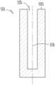
- FIG. 1 Ashows an example of a cross-sectional depiction of a vertical feature 101 to be filled with tungsten.
- the featurecan include a feature hole 105 in a substrate 103 .
- the substratemay be a silicon wafer, e.g., 200-mm wafer, 300-mm wafer, 450-mm wafer, including wafers having one or more layers of material such as dielectric, conducting, or semi-conducting material deposited thereon.
- the feature hole 105may have an aspect ratio of at least about 2:1, at least about 4:1, at least about 6:1, or higher.
- the feature hole 105may also have a dimension near the opening, e.g., an opening diameter or line width, of between about 10 nm to 500 nm (for example, between about 25 nm to 300 nm).
- the feature hole 105can be referred to as an unfilled feature or simply a feature.
- the feature, and any featuremay be characterized in part by an axis 118 that extends through the length of the feature, with vertically-oriented features having vertical axes and horizontally-oriented features having horizontal axes.
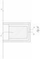
- FIG. 1 Bshows an example of a feature 101 that has a re-entrant profile.
- a re-entrant profileis a profile that narrows from a bottom, closed end, or interior of the feature to the feature opening. According to various embodiments, the profile may narrow gradually and/or include an overhang at the feature opening.
- FIG. 1 Bshows an example of the latter, with an underlayer 113 lining the sidewall or interior surfaces of the feature hole 105 .
- the underlayer 113can be, for example, a diffusion barrier layer, an adhesion layer, a nucleation layer, a combination of thereof, or any other applicable material.
- the underlayer 113forms an overhang 115 such that the underlayer 113 is thicker near the opening of the feature 101 than inside the feature 101 .
- FIG. 1 Cshows examples of views of various filled features having constrictions.
- Each of the examples (a), (b) and (c) in FIG. 1 Cincludes a constriction 109 at a midpoint within the feature.
- the constriction 109can be, for example, between about 15 nm-20 nm wide.
- Constrictionscan cause pinch off during deposition of tungsten in the feature using conventional techniques, with deposited tungsten blocking further deposition past the constriction before that portion of the feature is filled, resulting in voids in the feature.
- Example (b)further includes a liner/barrier overhang 115 at the feature opening. Such an overhang could also be a potential pinch-off point.
- Example (c)includes a constriction 112 further away from the field region than the overhang 115 in example (b). As described further below, methods described herein allow void-free fill as depicted in FIG. 1 C .
- FIG. 1 Dshows an example of a word line 150 in a VNAND structure 148 that includes a constriction 151 .
- the constrictionscan be due to the presence of pillars in a VNAND or other structure.
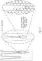
- FIG. 1 Eshows a plan view of pillars 125 in a VNAND structure, with FIG. 1 F showing a simplified schematic of a cross-sectional depiction of the pillars 125 .
- Arrows in FIG. 1 Erepresent deposition material; as pillars 125 are disposed between an area 127 and a gas inlet or other deposition source, adjacent pillars can result in constrictions that present challenges in void free fill of an area 127 .
- FIG. 1 Gprovides another example of a view horizontal feature, for example, of a VNAND or other structure including pillar constrictions 151 .
- the example in FIG. 1 Gis open-ended, with material to be deposited able to enter laterally from two sides as indicated by the arrows. (It should be noted that the example in FIG. 1 G can be seen as a two-dimensional (2D) rendering of 3D features of the structure, with the FIG.
- 3D structurescan be characterized with the area to be filled extending along three dimensions (e.g., in the X, Y, and Z-directions in the example of FIG. 1 F ) and can present more challenges for fill than filling holes or trenches that extend along one or two dimensions. For example, controlling fill of a 3D structure can be challenging as deposition gasses may enter a feature from multiple dimensions.
- Filling features with tungsten-containing materialsmay cause formation of voids and seams inside the filled features.
- a voidis region in the feature that is left unfilled.
- a voidcan form, for example, when the deposited material forms a pinch point within the feature, sealing off an unfilled space within the feature and preventing reactant entry and deposition.
- FIG. 1 BAnother cause of void or seam formation that is not illustrated in FIG. 1 B but that nevertheless may lead to seam formation or enlarging seams is curved (or bowed) side walls of feature holes, which are also referred to as bowed features.
- a bowed featurethe cross-sectional dimension of the cavity near the opening is smaller than that inside the feature. Effects of these narrower openings in the bowed features are somewhat similar to the overhang problem described above.
- Constrictions within a feature such as shown in FIGS. 1 C, 1 D, and 1 Galso present challenges for tungsten fill with few or no voids and seams.
- tungsten in the featuremay contain a seam running through the axis or middle of the via, trench, line, or another feature. This is because tungsten growth can begin at the sidewall and continue until the grains meet with tungsten growing from the opposite sidewall. This seam can allow for trapping of impurities including fluorine-containing compounds such as hydrofluoric acid (HF). During CMP, coring can also propagate from the seam. According to various embodiments, the methods described herein can reduce or eliminate void and seam formation. The methods described herein may also address one or more of the following:
- Void free fillcan be achieved in most re-entrant features using dep-etch-dep cycles as described in U.S. patent application Ser. No. 13/351,970, incorporated by reference herein. However, depending on the dimensions and geometry, multiple dep-etch cycles may be needed to achieve void-free fill. This can affect process stability and throughput. Embodiments described herein can provide feature fill with fewer or no dep-etch-dep cycles.
- Reduced via volume for W fillEspecially in smaller and newer features, a significant part of the metal contact is used up by the W barrier (TiN, WN etc.). These films are typically higher resistivity than W and negatively impact electrical characteristics like contact resistance and the like.
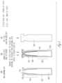
- FIG. 1 Hdepicts a schematic example of a DRAM architecture including a bWL 11 in a silicon substrate 9 .
- the bWLis formed in a trench etched in the silicon substrate 9 .
- Lining the trenchis a conformal barrier layer 12 and an insulating layer 13 that is disposed between the conformal barrier layer 12 and the silicon substrate 9 .
- the insulating layer 13may be a gate oxide layer formed from a high-k dielectric material such as a silicon oxide or silicon nitride material.
- conformal barrier layersinclude tungsten-containing layers and titanium nitride (TiN). Tungsten-containing conformal barrier layers are described in U.S. patent application Ser. No. 15/051,561, which is incorporated by reference herein.
- FIG. 1 Ishows an unfilled and filled narrow asymmetric trench structure typical of DRAM bWL.
- the unfilled featuresare adjacent and generally V-shaped, having sloped sidewalls. The features widen from the feature bottom to the feature top. After tungsten fill, severe line bending is observed. Without being bound by a particular theory, it is believed that a cohesive force between opposing surfaces of a trench pulls the trench sides together. This phenomenon is illustrated in FIG. 1 J and may be characterized as “zipping up” the feature. As the feature is filled, more force is exerted from a center axis of the feature, causing line bending.
- FIG. 1 Killustrates the interatomic force as a function of tungsten-tungsten bond radius, r. As can be seen, a cohesive force exists at certain values of r.
- the pitch(feature to feature distance from feature center axes) is below 50 nm, below 40 nm, or below 30 nm.
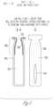
- FIG. 6shows an example of a feature hole 105 including an underlayer 113 , which can be, for example, a metal nitride or other barrier layer.
- a tungsten layer 653is conformally deposited in the feature hole 10 , for example, by a Pulsed Nucleation Layer (PNL) and/or CVD method. (Note that while the tungsten layer 653 is conformally deposited in the feature hole 105 in the example of FIG.
- PNLPulsed Nucleation Layer
- tungsten nucleation on the underlayer 113can be selectively inhibited prior to selective deposition of the tungsten layer 653 .
- Further deposition on the tungsten layer 653is then selectively inhibited, forming inhibited portion 655 of the tungsten layer 653 near the feature opening.
- Tungstenis then selectively deposited by a PNL and/or CVD method in accordance with the inhibition profile such that tungsten is preferentially deposited near the bottom and mid-section of the feature. Deposition continues, in some embodiments, with one or more selective inhibition cycles until the feature is filled.
- the inhibition effect at the feature topcan be overcome by a long enough deposition time, while in some embodiments, an additional nucleation layer deposition or other treatment may be performed to lessen or remove the passivation at the feature opening once deposition there is desired.
- feature fillmay still include formation of a seam, such as seam 657 depicted in FIG. 6 .
- the sequence depicted in the example of FIG. 6may end post-CMP with a relatively small void still present.
- FIG. 2shows schematic diagrams of two features 202 and 204 .
- Feature 202has a re-entrant geometry and feature 204 has a V-shaped geometry.
- the features 202 and 204have been formed using deposition only at ultra-low stress deposition conditions.
- WF6tungsten hexafluoride
- Attempts to cure such voids 206 and 208have included inhibition, and the use of inhibiting precursor gases.
- One such techniqueis known as inhibition chemistry enhancement, or ICE.
- a conformal nucleation (nuc) layer 304is formed by a first deposition (dep 1 ).
- a conformal inhibition (or ICE) layer 306is formed over an upper region 308 of the nucleation layer 304 , as shown.
- a second deposition (or dep 2 )forms a nonconformal bulk layer 310 for the completed feature 302 shown on the right.
- the inhibition ICE layer 306is intended to inhibit growth of the bulk later 310 to keep the mouth (or restriction) 312 of the trench 316 open during fill (e.g., W-fill). This effect may also be expressed as a differentiation ICE effect. Notwithstanding the differentiation effect of the inhibition layer 306 , a void 314 has nevertheless been formed.
- Selective inhibitionwhich may also be referred to as selective passivation, differential inhibition, or differential passivation, involves inhibiting subsequent tungsten nucleation on a portion of the feature, while not inhibiting nucleation (or inhibiting nucleation to a lesser extent) on the remainder of the feature.
- a featureis selectively inhibited at a feature opening, while nucleation inside the feature is not inhibited.
- Selective inhibitioncan involve, for example, selectively exposing a portion of the feature to activated species of a plasma.
- a feature openingis selectively exposed to a plasma generated from molecular nitrogen gas.
- a desired inhibition profile in a featurecan be formed by appropriately selecting one or more of inhibition chemistry, substrate bias power, plasma power, process pressure, exposure time, and other process parameters. Further aspects relating to the formation of inhibition profiles and differential inhibition are described in U.S. patent application Ser. No. 15/640,940, incorporated by reference herein.
- tungsten hexafluorideAs noted above, low flow levels of tungsten hexafluoride (WF6) and higher temperatures lead to WF6 depletion.
- a WF6 depleted environmenttypically calls for a strong, conformal ICE layer 306 to withstand, or inhibit, rapid creation of the bulk layer 310 at the mouth 312 thereof so that the mouth 312 remains clear to admit fill allowing the trench 316 to be filled completely. But in the example of FIG. 3 , sufficient inhibition (or a desired inhibition profile) has not occurred.
- the illustrated mouth 312has closed off prematurely and the void 314 has been formed due to a lack of fill reaching it. It will be appreciated that such voids can significantly negatively affect device performance.
- the avoidance of voids 314can be particularly problematic in the formation of very high aspect features and in filling deep trenches, vias, and the like.
- a desired inhibition profilemay be created based on several factors. Factors may include the growth retarding effect of a given inhibition layer, a nature (e.g., conformality) or condition (e.g., stress) of an underlying nucleation or deposition layer to which the inhibition layer is applied, and chamber processing conditions, among others.
- Factorsmay include the growth retarding effect of a given inhibition layer, a nature (e.g., conformality) or condition (e.g., stress) of an underlying nucleation or deposition layer to which the inhibition layer is applied, and chamber processing conditions, among others.
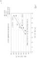
- the y axis of graph 400depicts a final stack height or thickness (THK) of the films in Angstrom (A) during a deposition operation (for example, during (dep 2 )).
- the x axisdepicts corresponding CVD times in seconds during the deposition.
- the slope ( ⁇ y/ ⁇ x) of a linear line 402 or 404may be considered to represent a speed of growth of the films (i.e., rate of thickness growth over time).
- the linear line 402represents a growth profile for an example film formed by applying a thermal inhibition layer (ICE) to a nucleation layer (nuc) alone.
- the linear line 404represents a growth profile for an example film formed by applying a thermal inhibition layer (ICE) to a bulk layer (or cool film (CF)).
- linear line 404(i.e., representing a film growth profile) has “shifted” (or at least appears) to the right in the graph 400 as compared to linear line 402 .
- the film formed in the circumstances of linear line 404has taken longer (there has been a “delay”) to reach the same height as the film of linear line 402 , even though the rate of growth (slope) of the respective films has been substantially the same.
- the thickness of the film of line 404has lagged that of the film of line 402 .
- the “difference”may be expressed as approximately 500-1000 A.
- differential effectmay be multiplied or enhanced accordingly.
- a “difference” (or inhibition profile) between two layers facing each other on either side of a trench, with each layer having undergone the same inhibitionmay be considered to have doubled (i.e., 1000-2000 A, or more in some examples).
- the inhibition or “differential effect” of the inhibition layer used in the examples of lines 402 and 404has thus been different based primarily, in this example, on the nature and type of film to which the inhibition layer has been applied (i.e., nucleation versus bulk).
- High aspect features and growth profilesmay be formed using improved selective inhibition accordingly, in conformance with examples of the present disclosure.
- Some examplesinclude the maintenance of free passage for fill material within features during fill operations and, in some examples, the complete removal of voids. In this regard, reference is now made to FIG. 5 .
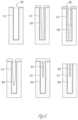
- FIG. 5illustrates example operations in an example method of the present disclosure.
- a trench 502is to be filled to form a feature 504 in the various phases shown in the views of operations 506 through 510 .
- a conformal nucleation layer 512is formed on an interior surface of the trench 502 .
- a nonconformal bulk layer 514is then formed over the nucleation layer 512 in an upper region 516 of the trench 502 , as shown.
- the upper region 516is adjacent the open mouth of the trench 502 which, as discussed above, may conventionally be prone to closure, thereby disallowing a complete fill and the formation of voids in the feature 504 .
- the formation of the nonconformal bulk layer 514may occur in an initial nonconformal deposition phase (dep 1 , operation 506 ).
- a small degree of overburden 518may appear on the substrate field adjacent the open mouth of the trench 502 .
- the nonconformal bulk layer 514is applied over the nucleation layer 512 before the application of an inhibition layer.
- an inhibition layer 520is applied over the nonconformal bulk layer 514 and to interior surfaces of the trench 502 as shown.
- the inhibition layer 520is applied to the nonconformal bulk layer 514 in an upper region 516 of the trench and the nucleation layer 512 in an intermediate region 522 of the trench, but is not applied to the nucleation layer 512 in a inhibition-free lower region 524 of the trench 502 .
- the upper region 516 of the trench 502corresponds to a boundary of an outer surface of the nonconformal bulk layer 514 interposed between the conformal nucleation layer 512 and the inhibition layer 520 .
- the nonconformal bulk layer 514(or any layer) has not been formed and the inhibition layer 520 lies directly on the nucleation layer 512 .
- the differential effect of an inhibition layer on a bulk layeris strong, whereas its inhibition effect on a nucleation layer is relatively weak.
- the trenchis filled in a subsequent deposition operation (e.g., nonconformal dep 2 ).
- a subsequent deposition operatione.g., nonconformal dep 2
- the strong inhibition effect of the inhibition layer 520 in upper region 516 , adjacent the mouth of the trenchkeeps the mouth free.
- dep 2for example
- the nonconformal bulk film in that regiongrows slowly, whereas film in the weaker inhibition zone lower down in intermediate region 522 grows relatively faster.
- the growth of film adjacent the mouthis “delayed” in the manner discussed further above.
- the differential inhibitionor growth profile
- the selective formation of an initial nonconformal bulk layer inside a feature, before an inhibition layer is appliedcan enhance inhibition or differentiation effects therein to provide a void-free fill, at least in some examples.
- a methodmay comprise providing a substrate including a feature having one or more feature openings and a feature interior; forming a nucleation layer on a surface of the feature interior; based on a differential inhibition profile, selectively forming a nonconformal bulk layer on the surface of the nucleation layer to leave regions of the nucleation layer covered and uncovered by the nonconformal bulk layer; selectively forming an inhibition layer on the covered and uncovered regions of the nucleation layer; and selectively depositing tungsten in the feature in accordance with the differential inhibition profile.
- inventive subject mattermay be referred to herein, individually and/or collectively, by the term “invention” merely for convenience and without intending to voluntarily limit the scope of this application to any single invention or inventive concept if more than one is in fact disclosed.
- inventive conceptmerely for convenience and without intending to voluntarily limit the scope of this application to any single invention or inventive concept if more than one is in fact disclosed.
Landscapes
- Engineering & Computer Science (AREA)
- Microelectronics & Electronic Packaging (AREA)
- Condensed Matter Physics & Semiconductors (AREA)
- General Physics & Mathematics (AREA)
- Manufacturing & Machinery (AREA)
- Computer Hardware Design (AREA)
- Physics & Mathematics (AREA)
- Power Engineering (AREA)
- Chemical & Material Sciences (AREA)
- Crystallography & Structural Chemistry (AREA)
- Internal Circuitry In Semiconductor Integrated Circuit Devices (AREA)
- Electrodes Of Semiconductors (AREA)
- Semiconductor Memories (AREA)
- Chemical Vapour Deposition (AREA)
Abstract
Description
Claims (10)
Priority Applications (1)
| Application Number | Priority Date | Filing Date | Title |
|---|---|---|---|
| US17/430,633US12261081B2 (en) | 2019-02-13 | 2020-02-13 | Tungsten feature fill with inhibition control |
Applications Claiming Priority (3)
| Application Number | Priority Date | Filing Date | Title |
|---|---|---|---|
| US201962805197P | 2019-02-13 | 2019-02-13 | |
| US17/430,633US12261081B2 (en) | 2019-02-13 | 2020-02-13 | Tungsten feature fill with inhibition control |
| PCT/US2020/018103WO2020168071A1 (en) | 2019-02-13 | 2020-02-13 | Tungsten feature fill with inhibition control |
Publications (2)
| Publication Number | Publication Date |
|---|---|
| US20220172987A1 US20220172987A1 (en) | 2022-06-02 |
| US12261081B2true US12261081B2 (en) | 2025-03-25 |
Family
ID=72044811
Family Applications (1)
| Application Number | Title | Priority Date | Filing Date |
|---|---|---|---|
| US17/430,633Active2041-10-10US12261081B2 (en) | 2019-02-13 | 2020-02-13 | Tungsten feature fill with inhibition control |
Country Status (6)
| Country | Link |
|---|---|
| US (1) | US12261081B2 (en) |
| JP (1) | JP7705349B2 (en) |
| KR (1) | KR20210117343A (en) |
| CN (1) | CN113424308B (en) |
| SG (1) | SG11202108725XA (en) |
| WO (1) | WO2020168071A1 (en) |
Cited By (2)
| Publication number | Priority date | Publication date | Assignee | Title |
|---|---|---|---|---|
| US12387979B2 (en) | 2012-03-27 | 2025-08-12 | Novellus Systems, Inc. | Tungsten feature fill with nucleation inhibition |
| US12444651B2 (en) | 2022-06-28 | 2025-10-14 | Novellus Systems, Inc. | Tungsten feature fill with nucleation inhibition |
Families Citing this family (9)
| Publication number | Priority date | Publication date | Assignee | Title |
|---|---|---|---|---|
| JP7705349B2 (en) | 2019-02-13 | 2025-07-09 | ラム リサーチ コーポレーション | Tungsten feature filling with inhibition control |
| US11482452B2 (en)* | 2020-12-24 | 2022-10-25 | Wonik Ips Co., Ltd | Method of forming a contact plug in a semiconductor integrated circuit device |
| KR20240005861A (en)* | 2021-05-06 | 2024-01-12 | 어플라이드 머티어리얼스, 인코포레이티드 | Processing systems and methods to improve productivity of void-free and gap-free tungsten gapfill processes |
| US12037682B2 (en) | 2021-10-05 | 2024-07-16 | Applied Materials, Inc. | Methods for forming low resistivity tungsten features |
| TW202401671A (en)* | 2021-12-13 | 2024-01-01 | 美商蘭姆研究公司 | Tungsten wordline fill in high aspect ratio 3d nand architecture |
| US12217965B2 (en) | 2022-01-11 | 2025-02-04 | Sandisk Technologies Llc | Methods and apparatuses for forming semiconductor devices containing tungsten layers using a tungsten growth suppressant |
| US12176203B2 (en) | 2022-01-11 | 2024-12-24 | Sandisk Technologies Llc | Methods and apparatuses for forming semiconductor devices containing tungsten layers using a tungsten growth suppressant |
| WO2023136854A1 (en)* | 2022-01-11 | 2023-07-20 | Sandisk Technologies Llc | Methods and apparatuses for forming semiconductor devices containing tungsten layers using a tungsten growth suppressant |
| US12159804B2 (en) | 2022-03-09 | 2024-12-03 | Applied Materials, Inc. | Tungsten molybdenum structures |
Citations (165)
| Publication number | Priority date | Publication date | Assignee | Title |
|---|---|---|---|---|
| US4714520A (en) | 1985-07-25 | 1987-12-22 | Advanced Micro Devices, Inc. | Method for filling a trench in an integrated circuit structure without producing voids |
| JPH0225568A (en) | 1988-07-15 | 1990-01-29 | Hitachi Ltd | How to fill micro holes in metal |
| JPH02187031A (en) | 1989-01-14 | 1990-07-23 | Sharp Corp | Semiconductor device |
| JPH03110840A (en) | 1989-09-26 | 1991-05-10 | Canon Inc | Deposited film formation method |
| EP0430303A2 (en) | 1989-12-01 | 1991-06-05 | Applied Materials, Inc. | Improved process for selective deposition of tungsten on semiconductor wafer |
| US5112439A (en) | 1988-11-30 | 1992-05-12 | Mcnc | Method for selectively depositing material on substrates |
| JPH04142061A (en) | 1990-10-02 | 1992-05-15 | Sony Corp | Formation of tungsten plug |
| JPH05226280A (en) | 1992-02-14 | 1993-09-03 | Matsushita Electric Ind Co Ltd | Manufacture of semiconductor device |
| JPH0794488A (en) | 1993-09-20 | 1995-04-07 | Tokyo Electron Ltd | Cleaning method of vacuum treatment device assembly |
| US5407698A (en) | 1992-04-29 | 1995-04-18 | Northern Telecom Limited | Deposition of tungsten |
| JPH07147321A (en) | 1993-11-26 | 1995-06-06 | Nec Corp | Manufacture of semiconductor device |
| JPH07226393A (en) | 1994-02-15 | 1995-08-22 | Sony Corp | Method and apparatus for dry-etching |
| US5504038A (en) | 1995-05-25 | 1996-04-02 | United Microelectronics Corporation | Method for selective tungsten sidewall and bottom contact formation |
| JPH0922896A (en) | 1995-07-07 | 1997-01-21 | Toshiba Corp | Selective metal film formation method |
| KR19980011846U (en) | 1996-08-23 | 1998-05-25 | 맹섭 | Stirrups for Golf Bags |
| US5785796A (en) | 1993-09-17 | 1998-07-28 | Tokyo Electron Limited | Vacuum processing apparatus, vacuum processing method, and method for cleaning the vacuum processing apparatus |
| US5963827A (en) | 1993-04-06 | 1999-10-05 | Sony Corporation | Method for producing via contacts in a semiconductor device |
| US6025243A (en) | 1989-09-26 | 2000-02-15 | Canon Kabushiki Kaisha | Method for preparing a semiconductor device |
| KR20010030488A (en) | 1999-09-21 | 2001-04-16 | 조셉 제이. 스위니 | A multistep chamber cleaning process using a remote plasma that also enhances film gap fill |
| US6245654B1 (en) | 1999-03-31 | 2001-06-12 | Taiwan Semiconductor Manufacturing Company, Ltd | Method for preventing tungsten contact/via plug loss after a backside pressure fault |
| KR20010048302A (en) | 1999-11-26 | 2001-06-15 | 박종섭 | Contact forming method for semiconductor device |
| US6339023B1 (en) | 1998-04-10 | 2002-01-15 | Applied Materials Inc. | Method of reducing stress in blanket tungsten film formed by chemical vapor deposition process |
| JP2002016066A (en) | 2000-06-27 | 2002-01-18 | Mitsubishi Electric Corp | Semiconductor device and method of manufacturing the same |
| US20020090811A1 (en) | 2001-01-08 | 2002-07-11 | Kim Byung-Hee | Method of fabricating metal lines in a semiconductor device |
| US20020132472A1 (en) | 2001-03-14 | 2002-09-19 | Jusung Engineering Co., Ltd. | Method for forming metal plug |
| JP2002294449A (en) | 2001-03-28 | 2002-10-09 | Fujitsu Ltd | Method for forming tungsten film and apparatus for forming tungsten film |
| US20020192953A1 (en) | 2001-06-19 | 2002-12-19 | Yu-Piao Wang | Method for forming a plug metal layer |
| JP2003022985A (en) | 2001-07-10 | 2003-01-24 | Matsushita Electric Ind Co Ltd | Semiconductor device manufacturing method and its manufacturing apparatus |
| US20030042465A1 (en) | 2001-08-30 | 2003-03-06 | Micron Technology, Inc. | Etchant gas composition |
| US20030082902A1 (en) | 2001-10-31 | 2003-05-01 | Shoichi Fukui | Semiconductor-device fabrication method |
| US20030092280A1 (en) | 2001-11-09 | 2003-05-15 | Applied Materials, Inc. | Method for etching tungsten using NF3 and Cl2 |
| US6602782B2 (en) | 2000-05-31 | 2003-08-05 | Samsung Electronics Co., Ltd. | Methods for forming metal wiring layers and metal interconnects and metal interconnects formed thereby |
| US20030194850A1 (en) | 2002-04-16 | 2003-10-16 | Applied Materials, Inc. | Method and apparatus for improved electroplating fill of an aperture |
| US20030203123A1 (en) | 2002-04-26 | 2003-10-30 | Applied Materials, Inc. | System and method for metal induced crystallization of polycrystalline thin film transistors |
| US6641867B1 (en)* | 1998-03-31 | 2003-11-04 | Texas Instruments Incorporated | Methods for chemical vapor deposition of tungsten on silicon or dielectric |
| US20030222346A1 (en) | 2002-05-30 | 2003-12-04 | Yun Ju-Young | Methods of forming metal interconnections of semiconductor devices by treating a barrier metal layer, and semiconductor devices including an oxide of a barrier layer |
| US20040149386A1 (en) | 2001-05-17 | 2004-08-05 | Yoichiro Numasawa | Plasma processing device and method of cleaning the same |
| US6790773B1 (en) | 2002-08-28 | 2004-09-14 | Novellus Systems, Inc. | Process for forming barrier/seed structures for integrated circuits |
| KR20040087406A (en) | 2003-04-07 | 2004-10-14 | 아남반도체 주식회사 | Fabricating method of semiconductor device |
| US20050014365A1 (en) | 2003-07-15 | 2005-01-20 | Moon Kwang-Jin | Methods of forming cobalt layers for semiconductor devices |
| US20050147762A1 (en) | 2003-12-30 | 2005-07-07 | Dubin Valery M. | Method to fabricate amorphous electroless metal layers |
| KR20050087428A (en) | 2004-02-26 | 2005-08-31 | 노벨러스 시스템즈, 인코포레이티드 | Deposition of tungsten nitride |
| US20060009034A1 (en) | 2000-06-28 | 2006-01-12 | Lai Ken K | Methods for depositing tungsten layers employing atomic layer deposition techniques |
| US20060075966A1 (en) | 2002-01-26 | 2006-04-13 | Applied Materials, Inc. | Apparatus and method for plasma assisted deposition |
| EP1672687A1 (en) | 2004-12-17 | 2006-06-21 | Interuniversitair Microelektronica Centrum ( Imec) | Formation of deep airgap trenches and related applications |
| CN1798867A (en) | 2003-01-09 | 2006-07-05 | 微米技术股份有限公司 | Deposition chamber surface enhancement and resulting deposition chambers |
| KR20060087844A (en) | 2005-01-31 | 2006-08-03 | 삼성전자주식회사 | Semiconductor device and manufacturing method thereof |
| US20060265100A1 (en) | 2001-02-13 | 2006-11-23 | Micron Technology, Inc. | Sequential pulse deposition |
| CN1883037A (en) | 2003-11-19 | 2006-12-20 | 东京毅力科创株式会社 | Plasma processing method and plasma processing apparatus |
| WO2007027350A2 (en) | 2005-08-02 | 2007-03-08 | Massachusetts Institute Of Technology | Method of removing surface deposits and passivating interior surfaces of the interior of a chemical vapour deposition (cvd) chamber |
| US20070066060A1 (en) | 2005-09-19 | 2007-03-22 | Taiwan Semiconductor Manufacturing Co., Ltd. | Semiconductor devices and fabrication methods thereof |
| KR20070054100A (en) | 2005-11-22 | 2007-05-28 | 에어 프로덕츠 앤드 케미칼스, 인코오포레이티드 | Selective Etching Method of Titanium Nitride Using Xenon Difluoride |
| US20070166989A1 (en) | 2005-05-18 | 2007-07-19 | Intermolecular, Inc. | Substrate processing including a masking layer |
| US20070199922A1 (en) | 2006-02-27 | 2007-08-30 | Applied Materials, Inc. | Etch methods to form anisotropic features for high aspect ratio applications |
| KR100757418B1 (en) | 2006-09-05 | 2007-09-10 | 삼성전자주식회사 | Semiconductor element and method of forming the same |
| JP2007251164A (en) | 2006-03-15 | 2007-09-27 | Internatl Business Mach Corp <Ibm> | Interconnect structure, semiconductor structure and method of forming interconnect structure (formation of oxidation-resistant seed layer for interconnect usage) |
| US20070264105A1 (en) | 2006-05-12 | 2007-11-15 | Axcelis Technologies Inc. | Combination load lock for handling workpieces |
| KR20080001460A (en) | 2006-06-29 | 2008-01-03 | 주식회사 하이닉스반도체 | Tungsten film formation method of semiconductor device and tungsten wiring layer formation method using same |
| JP2008049976A (en) | 2006-08-28 | 2008-03-06 | Toyota Motor Corp | Vehicle communication system, task activation method, and cycle timer activation method |
| CN101154576A (en) | 2006-09-29 | 2008-04-02 | 海力士半导体有限公司 | Method of forming tungsten polymetallic gates with low resistance |
| US20080081470A1 (en) | 2006-09-29 | 2008-04-03 | Tokyo Electron Limited | Method for forming strained silicon nitride films and a device containing such films |
| US20080079156A1 (en) | 2006-09-29 | 2008-04-03 | Hynix Semiconductor Inc. | Metal line in semiconductor device and method for forming the same |
| CN101213320A (en) | 2005-07-01 | 2008-07-02 | 东京毅力科创株式会社 | Method for forming tungsten film, film forming apparatus, storage medium, and semiconductor device |
| KR20080061978A (en) | 2006-12-28 | 2008-07-03 | 주식회사 하이닉스반도체 | Wiring Formation Method of Semiconductor Device |
| JP2008177577A (en) | 2007-01-18 | 2008-07-31 | Samsung Electronics Co Ltd | Semiconductor device, method for forming the same, and semiconductor cluster equipment |
| US20080254623A1 (en) | 2001-05-22 | 2008-10-16 | Novellus Systems, Inc. | Methods for growing low-resistivity tungsten for high aspect ratio and small features |
| KR20080094088A (en) | 2006-01-31 | 2008-10-22 | 도쿄엘렉트론가부시키가이샤 | Seed film forming method, plasma film forming apparatus and storage medium |
| US20080268635A1 (en)* | 2001-07-25 | 2008-10-30 | Sang-Ho Yu | Process for forming cobalt and cobalt silicide materials in copper contact applications |
| CN101308794A (en) | 2007-05-15 | 2008-11-19 | 应用材料股份有限公司 | Atomic Layer Deposition of Tungsten Materials |
| CN101313085A (en) | 2005-08-02 | 2008-11-26 | 麻省理工学院 | Method of removing surface deposits and passivating interior surfaces of the interior of a chemical vapour deposition (cvd) chamber |
| US20090004850A1 (en)* | 2001-07-25 | 2009-01-01 | Seshadri Ganguli | Process for forming cobalt and cobalt silicide materials in tungsten contact applications |
| US20090053426A1 (en) | 2001-07-25 | 2009-02-26 | Jiang Lu | Cobalt deposition on barrier surfaces |
| US20090053893A1 (en) | 2005-01-19 | 2009-02-26 | Amit Khandelwal | Atomic layer deposition of tungsten materials |
| WO2009042913A1 (en) | 2007-09-28 | 2009-04-02 | Sandisk 3D, Llc | Multiple antifuse memory cells and methods to form, program, and sense the same |
| CN101447427A (en) | 2007-11-30 | 2009-06-03 | 海力士半导体有限公司 | Method for forming tungsten film and method for forming wiring of semiconductor device using the same |
| US20090149022A1 (en) | 2007-12-05 | 2009-06-11 | Novellus Systems, Inc. | Method for improving uniformity and adhesion of low resistivity tungsten film |
| KR20090068187A (en) | 2007-12-21 | 2009-06-25 | 노벨러스 시스템즈, 인코포레이티드 | Method for forming all-tungsten junctions and lines |
| KR20090074560A (en) | 2008-01-02 | 2009-07-07 | 주식회사 하이닉스반도체 | Tungsten Film Formation Method of Semiconductor Device |
| US7569913B2 (en) | 2006-10-26 | 2009-08-04 | Atmel Corporation | Boron etch-stop layer and methods related thereto |
| US7655567B1 (en) | 2007-07-24 | 2010-02-02 | Novellus Systems, Inc. | Methods for improving uniformity and resistivity of thin tungsten films |
| US20100072623A1 (en) | 2008-09-19 | 2010-03-25 | Advanced Micro Devices, Inc. | Semiconductor device with improved contact plugs, and related fabrication methods |
| US20100130002A1 (en) | 2008-11-25 | 2010-05-27 | Dao Thuy B | Multilayered through via |
| US20100144140A1 (en) | 2008-12-10 | 2010-06-10 | Novellus Systems, Inc. | Methods for depositing tungsten films having low resistivity for gapfill applications |
| US20100159694A1 (en) | 2008-06-12 | 2010-06-24 | Novellus Systems Inc. | Method for depositing thin tungsten film with low resistivity and robust micro-adhesion characteristics |
| US20100167527A1 (en) | 2008-12-31 | 2010-07-01 | Applied Materials, Inc. | Method of depositing tungsten film with reduced resistivity and improved surface morphology |
| CN101770978A (en) | 2008-12-31 | 2010-07-07 | Y·舒尔 | High aspect ratio plug fill process |
| CN101789369A (en) | 2010-01-28 | 2010-07-28 | 上海宏力半导体制造有限公司 | Etching method of polymetallic tungsten gate |
| US20100267230A1 (en) | 2009-04-16 | 2010-10-21 | Anand Chandrashekar | Method for forming tungsten contacts and interconnects with small critical dimensions |
| JP2011035366A (en) | 2009-08-04 | 2011-02-17 | Novellus Systems Inc | Method of depositing tungsten on feature with high aspect ratio |
| US20110045672A1 (en) | 2009-08-20 | 2011-02-24 | Applied Materials, Inc. | Multi-film stack etching with polymer passivation of an overlying etched layer |
| WO2011027834A1 (en) | 2009-09-02 | 2011-03-10 | 株式会社アルバック | METHOD FOR FORMING Co FILM AND METHOD FOR FORMING Cu WIRING FILM |
| CN102007573A (en) | 2008-04-29 | 2011-04-06 | 应用材料公司 | Selective cobalt deposition on copper surfaces |
| US20110111533A1 (en) | 2009-11-12 | 2011-05-12 | Bhadri Varadarajan | Uv and reducing treatment for k recovery and surface clean in semiconductor processing |
| TW201120233A (en) | 2009-08-07 | 2011-06-16 | Sigma Aldrich Co | High molecular weight alkyl-allyl cobalttricarbonyl complexes and use thereof for preparing dielectric thin films |
| US20110151670A1 (en) | 2007-11-21 | 2011-06-23 | Lam Research Corporation | Method of controlling etch microloading for a tungsten-containing layer |
| US20110233778A1 (en) | 2010-03-24 | 2011-09-29 | Applied Materials, Inc. | Formation of liner and barrier for tungsten as gate electrode and as contact plug to reduce resistance and enhance device performance |
| JP2011199021A (en) | 2010-03-19 | 2011-10-06 | Renesas Electronics Corp | Semiconductor device, and method for manufacturing the same |
| CN102224574A (en) | 2008-11-24 | 2011-10-19 | 应用材料股份有限公司 | Bottom-up plating using organic surface passivation and differential plating retardation |
| US20110256717A1 (en) | 2010-04-19 | 2011-10-20 | Samsung Electronics Co., Ltd. | Methods for fabricating semiconductor devices |
| JP2011228709A (en) | 2010-04-20 | 2011-11-10 | Micron Technology Inc | Flash memory having multi-level architecture |
| US20120009785A1 (en)* | 2010-07-09 | 2012-01-12 | Anand Chandrashekar | Depositing Tungsten Into High Aspect Ratio Features |
| KR20120005992A (en) | 2010-07-09 | 2012-01-17 | 노벨러스 시스템즈, 인코포레이티드 | Depositing Tungsten Inside High Aspect Ratio Features |
| US8129270B1 (en) | 2008-12-10 | 2012-03-06 | Novellus Systems, Inc. | Method for depositing tungsten film having low resistivity, low roughness and high reflectivity |
| US20120077342A1 (en) | 2010-09-27 | 2012-03-29 | Juwen Gao | Systems and methods for selective tungsten deposition in vias |
| US20120149213A1 (en) | 2010-12-09 | 2012-06-14 | Lakshminarayana Nittala | Bottom up fill in high aspect ratio trenches |
| CN102543835A (en) | 2010-12-15 | 2012-07-04 | 中国科学院微电子研究所 | Method for filling opening |
| US20120187305A1 (en) | 2011-01-21 | 2012-07-26 | Uchicago Argonne Llc | Microchannel plate detector and methods for their fabrication |
| CN102892922A (en) | 2010-03-17 | 2013-01-23 | 应用材料公司 | Method and apparatus for remote plasma source assisted silicon-containing film deposition |
| US20130062677A1 (en) | 2011-09-09 | 2013-03-14 | International Business Machines Corporation | Self-aligned bottom plate for metal high-k dielectric metal insulator metal (mim) embedded dynamic random access memory |
| CN103107120A (en) | 2006-08-30 | 2013-05-15 | 朗姆研究公司 | Processes and integrated systems for engineering a substrate surface for metal deposition |
| US20130171822A1 (en)* | 2009-08-04 | 2013-07-04 | Anand Chandrashekar | Tungsten feature fill with nucleation inhibition |
| WO2013148490A1 (en) | 2012-03-28 | 2013-10-03 | Applied Materials, Inc. | Method of enabling seamless cobalt gap-fill |
| WO2013148444A1 (en) | 2012-03-27 | 2013-10-03 | Novellus Systems, Inc. | Tungsten feature fill with nucleation inhibition |
| WO2013148880A1 (en) | 2012-03-27 | 2013-10-03 | Novellus Systems, Inc. | Tungsten feature fill |
| TW201413031A (en) | 2012-07-27 | 2014-04-01 | Novellus Systems Inc | Methods of improving tungsten contact resistance in small critical dimension features |
| JP2014063926A (en) | 2012-09-21 | 2014-04-10 | Toshiba Corp | Semiconductor device and method for manufacturing the same |
| US20140106083A1 (en) | 2012-10-11 | 2014-04-17 | Applied Materials, Inc. | Tungsten growth modulation by controlling surface composition |
| US20140120723A1 (en) | 2012-10-26 | 2014-05-01 | Xinyu Fu | Methods for depositing fluorine/carbon-free conformal tungsten |
| WO2014105477A1 (en) | 2012-12-28 | 2014-07-03 | Intel Corporation | Cobalt based interconnects and methods of fabrication thereof |
| US20140231896A1 (en) | 2013-02-20 | 2014-08-21 | Kabushiki Kaisha Toshiba | Nonvolatile semiconductor storage device and method of manufacturing the same |
| EP2779224A2 (en) | 2013-03-15 | 2014-09-17 | Applied Materials, Inc. | Methods for producing interconnects in semiconductor devices |
| US20140264932A1 (en) | 2013-03-12 | 2014-09-18 | Taiwan Semiconductor Manufacturing Company, Ltd. | Patterning Approach to Reduce Via to Via Minimum Spacing |
| JP2014183185A (en) | 2013-03-19 | 2014-09-29 | Toshiba Corp | Semiconductor device manufacturing method and semiconductor device |
| CN104081502A (en) | 2012-02-17 | 2014-10-01 | 东京毅力科创株式会社 | Manufacturing method of semiconductor device |
| US20140349477A1 (en)* | 2013-05-24 | 2014-11-27 | Lam Research Corporation | Methods and apparatuses for void-free tungsten fill in three-dimensional semiconductor features |
| US20150024592A1 (en)* | 2009-08-04 | 2015-01-22 | Lam Research Corporation | Void free tungsten fill in different sized features |
| US20150091175A1 (en) | 2013-09-27 | 2015-04-02 | Manish Chandhok | Interconnects with fully clad lines |
| US20150093890A1 (en) | 2013-09-27 | 2015-04-02 | James M. Blackwell | Cobalt metal precursors |
| CN104513973A (en) | 2013-09-30 | 2015-04-15 | 朗姆研究公司 | High selectivity and low stress carbon dura mater achieved by pulsed low frequency RF power |
| US20150162214A1 (en) | 2013-12-09 | 2015-06-11 | Applied Materials, Inc. | Methods Of Selective Layer Deposition |
| CN104752339A (en) | 2013-12-27 | 2015-07-01 | 朗姆研究公司 | Tungsten Nucleation Process for Low Resistivity Tungsten Feature Fill |
| CN104975268A (en) | 2015-06-03 | 2015-10-14 | 武汉新芯集成电路制造有限公司 | Preparation method of metal tungsten thin film |
| US20150294906A1 (en) | 2014-04-11 | 2015-10-15 | Applied Materials, Inc. | Methods for forming metal organic tungsten for middle of the line (mol) applications |
| US20150361547A1 (en) | 2014-06-13 | 2015-12-17 | Taiwan Semiconductor Manufacturing Co., Ltd | Method and apparatus for cleaning chemical vapor deposition chamber |
| US20160020169A1 (en) | 2014-07-17 | 2016-01-21 | Kabushiki Kaisha Toshiba | Semiconductor device and method of manufacturing the same |
| US20160056077A1 (en) | 2014-08-21 | 2016-02-25 | Lam Research Corporation | Method for void-free cobalt gap fill |
| US20160056074A1 (en) | 2014-08-21 | 2016-02-25 | Lam Research Corporation | Method for void-free cobalt gap fill |
| CN105405764A (en) | 2014-07-25 | 2016-03-16 | 中国科学院微电子研究所 | Semiconductor device manufacturing method |
| US20160093528A1 (en)* | 2014-09-30 | 2016-03-31 | Lam Research Corporation | Feature fill with nucleation inhibition |
| KR20160044004A (en) | 2013-08-16 | 2016-04-22 | 어플라이드 머티어리얼스, 인코포레이티드 | Tungsten deposition with tungsten hexafluoride(wf6) etchback |
| US20160172211A1 (en) | 2014-12-15 | 2016-06-16 | Applied Materials, Inc. | Uv assisted cvd aln film for beol etch stop application |
| KR20160108174A (en) | 2015-03-04 | 2016-09-19 | 램 리써치 코포레이션 | Pretreatment of nickel and cobalt liners for electrodeposition of copper into through silicon vias |
| US20160293467A1 (en) | 2013-10-18 | 2016-10-06 | Brooks Automation, Inc. | Processing apparatus |
| US20160343612A1 (en)* | 2015-05-18 | 2016-11-24 | Lam Research Corporation | Feature fill with multi-stage nucleation inhibition |
| US20170053811A1 (en)* | 2015-08-21 | 2017-02-23 | Lam Research Corporation | Pulsing rf power in etch process to enhance tungsten gapfill performance |
| US20170125548A1 (en) | 2015-10-28 | 2017-05-04 | United Microelectronics Corp. | Semiconductor structure and fabrication method thereof |
| US20170229341A1 (en) | 2016-02-09 | 2017-08-10 | Taiwan Semiconductor Manufacturing Company, Ltd. | Method of Forming Trenches |
| US9837312B1 (en)* | 2016-07-22 | 2017-12-05 | Lam Research Corporation | Atomic layer etching for enhanced bottom-up feature fill |
| US20170365513A1 (en)* | 2012-03-27 | 2017-12-21 | Lam Research Corporation | Tungsten feature fill with nucleation inhibition |
| US20180053660A1 (en) | 2016-08-16 | 2018-02-22 | Lam Research Corporation | Method for preventing line bending during metal fill process |
| US20180174963A1 (en) | 2014-07-17 | 2018-06-21 | Taiwan Semiconductor Manufacturing Company, Ltd. | Conductive Structure and Method of Forming the Same |
| US20180174901A1 (en) | 2016-12-19 | 2018-06-21 | Lam Research Corporation | Chamber conditioning for remote plasma process |
| US20180308701A1 (en) | 2017-04-20 | 2018-10-25 | Lam Research Corporation | Methods and apparatus for forming smooth and conformal cobalt film by atomic layer deposition |
| US20180315650A1 (en)* | 2017-04-26 | 2018-11-01 | Applied Materials, Inc. | Process integration approach of selective tungsten via fill |
| US10193059B2 (en) | 2016-08-04 | 2019-01-29 | Industrial Technology Research Institute | Perpendicularly magnetized spin-orbit magnetic device |
| US20190326168A1 (en) | 2012-03-27 | 2019-10-24 | Novellus Systems, Inc. | Tungsten feature fill with nucleation inhibition |
| US20200083251A1 (en) | 2015-07-22 | 2020-03-12 | SK Hynix Inc. | Semiconductor device with high integration |
| WO2020168071A1 (en) | 2019-02-13 | 2020-08-20 | Lam Research Corporation | Tungsten feature fill with inhibition control |
| US20210028187A1 (en) | 2019-07-26 | 2021-01-28 | SK Hynix Inc. | Vertical semiconductor device and method for fabricating the same |
| US20210125832A1 (en) | 2019-10-25 | 2021-04-29 | Asm Ip Holding B.V. | Methods for filling a gap feature on a substrate surface and related semiconductor structures |
| US20220020641A1 (en) | 2018-12-05 | 2022-01-20 | Lam Research Corporation | Void free low stress fill |
| US20230041794A1 (en) | 2009-08-04 | 2023-02-09 | Novellus Systems, Inc. | Tungsten feature fill with nucleation inhibition |
| US20230122846A1 (en) | 2020-03-27 | 2023-04-20 | Lam Research Corporation | Feature fill with nucleation inhibition |
| US20230130557A1 (en) | 2020-03-04 | 2023-04-27 | Lam Research Corporation | Reactant gas pulse delivery |
| US20250038050A1 (en) | 2021-12-07 | 2025-01-30 | Lam Research Corporation | Feature fill with nucleation inhibition |
Family Cites Families (1)
| Publication number | Priority date | Publication date | Assignee | Title |
|---|---|---|---|---|
| JP3759525B2 (en)* | 2003-10-27 | 2006-03-29 | 松下電器産業株式会社 | Manufacturing method of semiconductor device |
- 2020
- 2020-02-13JPJP2021547160Apatent/JP7705349B2/enactiveActive
- 2020-02-13KRKR1020217029104Apatent/KR20210117343A/enactivePending
- 2020-02-13USUS17/430,633patent/US12261081B2/enactiveActive
- 2020-02-13WOPCT/US2020/018103patent/WO2020168071A1/ennot_activeCeased
- 2020-02-13SGSG11202108725XApatent/SG11202108725XA/enunknown
- 2020-02-13CNCN202080014189.3Apatent/CN113424308B/enactiveActive
Patent Citations (249)
| Publication number | Priority date | Publication date | Assignee | Title |
|---|---|---|---|---|
| US4714520A (en) | 1985-07-25 | 1987-12-22 | Advanced Micro Devices, Inc. | Method for filling a trench in an integrated circuit structure without producing voids |
| JPH0225568A (en) | 1988-07-15 | 1990-01-29 | Hitachi Ltd | How to fill micro holes in metal |
| US5112439A (en) | 1988-11-30 | 1992-05-12 | Mcnc | Method for selectively depositing material on substrates |
| JPH02187031A (en) | 1989-01-14 | 1990-07-23 | Sharp Corp | Semiconductor device |
| JPH03110840A (en) | 1989-09-26 | 1991-05-10 | Canon Inc | Deposited film formation method |
| US6025243A (en) | 1989-09-26 | 2000-02-15 | Canon Kabushiki Kaisha | Method for preparing a semiconductor device |
| EP0430303A2 (en) | 1989-12-01 | 1991-06-05 | Applied Materials, Inc. | Improved process for selective deposition of tungsten on semiconductor wafer |
| JPH04142061A (en) | 1990-10-02 | 1992-05-15 | Sony Corp | Formation of tungsten plug |
| JPH05226280A (en) | 1992-02-14 | 1993-09-03 | Matsushita Electric Ind Co Ltd | Manufacture of semiconductor device |
| US5407698A (en) | 1992-04-29 | 1995-04-18 | Northern Telecom Limited | Deposition of tungsten |
| US5963827A (en) | 1993-04-06 | 1999-10-05 | Sony Corporation | Method for producing via contacts in a semiconductor device |
| US5785796A (en) | 1993-09-17 | 1998-07-28 | Tokyo Electron Limited | Vacuum processing apparatus, vacuum processing method, and method for cleaning the vacuum processing apparatus |
| JPH0794488A (en) | 1993-09-20 | 1995-04-07 | Tokyo Electron Ltd | Cleaning method of vacuum treatment device assembly |
| JPH07147321A (en) | 1993-11-26 | 1995-06-06 | Nec Corp | Manufacture of semiconductor device |
| JPH07226393A (en) | 1994-02-15 | 1995-08-22 | Sony Corp | Method and apparatus for dry-etching |
| US5504038A (en) | 1995-05-25 | 1996-04-02 | United Microelectronics Corporation | Method for selective tungsten sidewall and bottom contact formation |
| JPH0922896A (en) | 1995-07-07 | 1997-01-21 | Toshiba Corp | Selective metal film formation method |
| US6013575A (en) | 1995-07-07 | 2000-01-11 | Kabushiki Kaisha Toshiba | Method of selectively depositing a metal film |
| KR19980011846U (en) | 1996-08-23 | 1998-05-25 | 맹섭 | Stirrups for Golf Bags |
| US6641867B1 (en)* | 1998-03-31 | 2003-11-04 | Texas Instruments Incorporated | Methods for chemical vapor deposition of tungsten on silicon or dielectric |
| US6339023B1 (en) | 1998-04-10 | 2002-01-15 | Applied Materials Inc. | Method of reducing stress in blanket tungsten film formed by chemical vapor deposition process |
| US6245654B1 (en) | 1999-03-31 | 2001-06-12 | Taiwan Semiconductor Manufacturing Company, Ltd | Method for preventing tungsten contact/via plug loss after a backside pressure fault |
| KR20010030488A (en) | 1999-09-21 | 2001-04-16 | 조셉 제이. 스위니 | A multistep chamber cleaning process using a remote plasma that also enhances film gap fill |
| US6503843B1 (en) | 1999-09-21 | 2003-01-07 | Applied Materials, Inc. | Multistep chamber cleaning and film deposition process using a remote plasma that also enhances film gap fill |
| KR20010048302A (en) | 1999-11-26 | 2001-06-15 | 박종섭 | Contact forming method for semiconductor device |
| US6602782B2 (en) | 2000-05-31 | 2003-08-05 | Samsung Electronics Co., Ltd. | Methods for forming metal wiring layers and metal interconnects and metal interconnects formed thereby |
| JP2002016066A (en) | 2000-06-27 | 2002-01-18 | Mitsubishi Electric Corp | Semiconductor device and method of manufacturing the same |
| US20060009034A1 (en) | 2000-06-28 | 2006-01-12 | Lai Ken K | Methods for depositing tungsten layers employing atomic layer deposition techniques |
| US20020090811A1 (en) | 2001-01-08 | 2002-07-11 | Kim Byung-Hee | Method of fabricating metal lines in a semiconductor device |
| US20060265100A1 (en) | 2001-02-13 | 2006-11-23 | Micron Technology, Inc. | Sequential pulse deposition |
| US20020132472A1 (en) | 2001-03-14 | 2002-09-19 | Jusung Engineering Co., Ltd. | Method for forming metal plug |
| JP2002294449A (en) | 2001-03-28 | 2002-10-09 | Fujitsu Ltd | Method for forming tungsten film and apparatus for forming tungsten film |
| US20040149386A1 (en) | 2001-05-17 | 2004-08-05 | Yoichiro Numasawa | Plasma processing device and method of cleaning the same |
| US8409985B2 (en) | 2001-05-22 | 2013-04-02 | Novellus Systems, Inc. | Methods for growing low-resistivity tungsten for high aspect ratio and small features |
| US20110223763A1 (en) | 2001-05-22 | 2011-09-15 | Lana Hiului Chan | Methods for growing low-resistivity tungsten for high aspect ratio and small features |
| US20080254623A1 (en) | 2001-05-22 | 2008-10-16 | Novellus Systems, Inc. | Methods for growing low-resistivity tungsten for high aspect ratio and small features |
| US20020192953A1 (en) | 2001-06-19 | 2002-12-19 | Yu-Piao Wang | Method for forming a plug metal layer |
| US20030190802A1 (en) | 2001-06-19 | 2003-10-09 | United Microelectronics Corp. | Method for forming a plug metal layer |
| JP2003022985A (en) | 2001-07-10 | 2003-01-24 | Matsushita Electric Ind Co Ltd | Semiconductor device manufacturing method and its manufacturing apparatus |
| US20090004850A1 (en)* | 2001-07-25 | 2009-01-01 | Seshadri Ganguli | Process for forming cobalt and cobalt silicide materials in tungsten contact applications |
| US20090053426A1 (en) | 2001-07-25 | 2009-02-26 | Jiang Lu | Cobalt deposition on barrier surfaces |
| US20080268635A1 (en)* | 2001-07-25 | 2008-10-30 | Sang-Ho Yu | Process for forming cobalt and cobalt silicide materials in copper contact applications |
| US20030042465A1 (en) | 2001-08-30 | 2003-03-06 | Micron Technology, Inc. | Etchant gas composition |
| US20030082902A1 (en) | 2001-10-31 | 2003-05-01 | Shoichi Fukui | Semiconductor-device fabrication method |
| US20030092280A1 (en) | 2001-11-09 | 2003-05-15 | Applied Materials, Inc. | Method for etching tungsten using NF3 and Cl2 |
| US20060075966A1 (en) | 2002-01-26 | 2006-04-13 | Applied Materials, Inc. | Apparatus and method for plasma assisted deposition |
| US20030194850A1 (en) | 2002-04-16 | 2003-10-16 | Applied Materials, Inc. | Method and apparatus for improved electroplating fill of an aperture |
| US20030203123A1 (en) | 2002-04-26 | 2003-10-30 | Applied Materials, Inc. | System and method for metal induced crystallization of polycrystalline thin film transistors |
| KR20030092583A (en) | 2002-05-30 | 2003-12-06 | 삼성전자주식회사 | Method for forming metal interconnections of semiconductor device |
| US20050179141A1 (en) | 2002-05-30 | 2005-08-18 | Yun Ju-Young | Methods of forming metal interconnections of semiconductor devices by treating a barrier metal layer |
| US20030222346A1 (en) | 2002-05-30 | 2003-12-04 | Yun Ju-Young | Methods of forming metal interconnections of semiconductor devices by treating a barrier metal layer, and semiconductor devices including an oxide of a barrier layer |
| US6790773B1 (en) | 2002-08-28 | 2004-09-14 | Novellus Systems, Inc. | Process for forming barrier/seed structures for integrated circuits |
| CN1798867A (en) | 2003-01-09 | 2006-07-05 | 微米技术股份有限公司 | Deposition chamber surface enhancement and resulting deposition chambers |
| KR20040087406A (en) | 2003-04-07 | 2004-10-14 | 아남반도체 주식회사 | Fabricating method of semiconductor device |
| KR100528073B1 (en) | 2003-04-07 | 2005-11-15 | 동부아남반도체 주식회사 | Fabricating method of semiconductor device |
| KR20050008320A (en) | 2003-07-15 | 2005-01-21 | 삼성전자주식회사 | Method for depositing cobalt layer |
| US20050014365A1 (en) | 2003-07-15 | 2005-01-20 | Moon Kwang-Jin | Methods of forming cobalt layers for semiconductor devices |
| CN1883037A (en) | 2003-11-19 | 2006-12-20 | 东京毅力科创株式会社 | Plasma processing method and plasma processing apparatus |
| US20050147762A1 (en) | 2003-12-30 | 2005-07-07 | Dubin Valery M. | Method to fabricate amorphous electroless metal layers |
| KR20050087428A (en) | 2004-02-26 | 2005-08-31 | 노벨러스 시스템즈, 인코포레이티드 | Deposition of tungsten nitride |
| EP1672687A1 (en) | 2004-12-17 | 2006-06-21 | Interuniversitair Microelektronica Centrum ( Imec) | Formation of deep airgap trenches and related applications |
| US20090053893A1 (en) | 2005-01-19 | 2009-02-26 | Amit Khandelwal | Atomic layer deposition of tungsten materials |
| KR20060087844A (en) | 2005-01-31 | 2006-08-03 | 삼성전자주식회사 | Semiconductor device and manufacturing method thereof |
| US20070166989A1 (en) | 2005-05-18 | 2007-07-19 | Intermolecular, Inc. | Substrate processing including a masking layer |
| CN101899649A (en) | 2005-07-01 | 2010-12-01 | 东京毅力科创株式会社 | Method for forming tungsten film |
| CN101213320A (en) | 2005-07-01 | 2008-07-02 | 东京毅力科创株式会社 | Method for forming tungsten film, film forming apparatus, storage medium, and semiconductor device |
| WO2007027350A2 (en) | 2005-08-02 | 2007-03-08 | Massachusetts Institute Of Technology | Method of removing surface deposits and passivating interior surfaces of the interior of a chemical vapour deposition (cvd) chamber |
| CN101313085A (en) | 2005-08-02 | 2008-11-26 | 麻省理工学院 | Method of removing surface deposits and passivating interior surfaces of the interior of a chemical vapour deposition (cvd) chamber |
| US20070066060A1 (en) | 2005-09-19 | 2007-03-22 | Taiwan Semiconductor Manufacturing Co., Ltd. | Semiconductor devices and fabrication methods thereof |
| KR20070054100A (en) | 2005-11-22 | 2007-05-28 | 에어 프로덕츠 앤드 케미칼스, 인코오포레이티드 | Selective Etching Method of Titanium Nitride Using Xenon Difluoride |
| US20090183984A1 (en) | 2006-01-31 | 2009-07-23 | Takashi Sakuma | Seed Film Forming Method, Plasma-Assisted Film Forming System and Storage Medium |
| KR20080094088A (en) | 2006-01-31 | 2008-10-22 | 도쿄엘렉트론가부시키가이샤 | Seed film forming method, plasma film forming apparatus and storage medium |
| US20070199922A1 (en) | 2006-02-27 | 2007-08-30 | Applied Materials, Inc. | Etch methods to form anisotropic features for high aspect ratio applications |
| JP2007251164A (en) | 2006-03-15 | 2007-09-27 | Internatl Business Mach Corp <Ibm> | Interconnect structure, semiconductor structure and method of forming interconnect structure (formation of oxidation-resistant seed layer for interconnect usage) |
| US20070264105A1 (en) | 2006-05-12 | 2007-11-15 | Axcelis Technologies Inc. | Combination load lock for handling workpieces |
| KR20080001460A (en) | 2006-06-29 | 2008-01-03 | 주식회사 하이닉스반도체 | Tungsten film formation method of semiconductor device and tungsten wiring layer formation method using same |
| JP2008049976A (en) | 2006-08-28 | 2008-03-06 | Toyota Motor Corp | Vehicle communication system, task activation method, and cycle timer activation method |
| CN103107120A (en) | 2006-08-30 | 2013-05-15 | 朗姆研究公司 | Processes and integrated systems for engineering a substrate surface for metal deposition |
| KR100757418B1 (en) | 2006-09-05 | 2007-09-10 | 삼성전자주식회사 | Semiconductor element and method of forming the same |
| US20080054468A1 (en) | 2006-09-05 | 2008-03-06 | Samsung Electronics Co., Ltd. | Semiconductor device and methods of forming the same |
| US20080079156A1 (en) | 2006-09-29 | 2008-04-03 | Hynix Semiconductor Inc. | Metal line in semiconductor device and method for forming the same |
| CN101154576A (en) | 2006-09-29 | 2008-04-02 | 海力士半导体有限公司 | Method of forming tungsten polymetallic gates with low resistance |
| US20080081470A1 (en) | 2006-09-29 | 2008-04-03 | Tokyo Electron Limited | Method for forming strained silicon nitride films and a device containing such films |
| US7569913B2 (en) | 2006-10-26 | 2009-08-04 | Atmel Corporation | Boron etch-stop layer and methods related thereto |
| KR20080061978A (en) | 2006-12-28 | 2008-07-03 | 주식회사 하이닉스반도체 | Wiring Formation Method of Semiconductor Device |
| JP2008177577A (en) | 2007-01-18 | 2008-07-31 | Samsung Electronics Co Ltd | Semiconductor device, method for forming the same, and semiconductor cluster equipment |
| CN101308794A (en) | 2007-05-15 | 2008-11-19 | 应用材料股份有限公司 | Atomic Layer Deposition of Tungsten Materials |
| JP2009024252A (en) | 2007-05-15 | 2009-02-05 | Applied Materials Inc | Atomic layer deposition of tungsten materials |
| US7655567B1 (en) | 2007-07-24 | 2010-02-02 | Novellus Systems, Inc. | Methods for improving uniformity and resistivity of thin tungsten films |
| WO2009042913A1 (en) | 2007-09-28 | 2009-04-02 | Sandisk 3D, Llc | Multiple antifuse memory cells and methods to form, program, and sense the same |
| JP2010541252A (en) | 2007-09-28 | 2010-12-24 | サンディスク スリーディー,エルエルシー | A plurality of antifuse memory cells and a method for forming, programming and detecting such memory cells |
| US20110151670A1 (en) | 2007-11-21 | 2011-06-23 | Lam Research Corporation | Method of controlling etch microloading for a tungsten-containing layer |
| CN101447427A (en) | 2007-11-30 | 2009-06-03 | 海力士半导体有限公司 | Method for forming tungsten film and method for forming wiring of semiconductor device using the same |
| US20090149022A1 (en) | 2007-12-05 | 2009-06-11 | Novellus Systems, Inc. | Method for improving uniformity and adhesion of low resistivity tungsten film |
| US20090163025A1 (en) | 2007-12-21 | 2009-06-25 | Novellus Systems, Inc. | Methods for forming all tungsten contacts and lines |
| KR20090068187A (en) | 2007-12-21 | 2009-06-25 | 노벨러스 시스템즈, 인코포레이티드 | Method for forming all-tungsten junctions and lines |
| KR20090074560A (en) | 2008-01-02 | 2009-07-07 | 주식회사 하이닉스반도체 | Tungsten Film Formation Method of Semiconductor Device |
| CN102007573A (en) | 2008-04-29 | 2011-04-06 | 应用材料公司 | Selective cobalt deposition on copper surfaces |
| US20100159694A1 (en) | 2008-06-12 | 2010-06-24 | Novellus Systems Inc. | Method for depositing thin tungsten film with low resistivity and robust micro-adhesion characteristics |
| US20100072623A1 (en) | 2008-09-19 | 2010-03-25 | Advanced Micro Devices, Inc. | Semiconductor device with improved contact plugs, and related fabrication methods |
| CN102224574A (en) | 2008-11-24 | 2011-10-19 | 应用材料股份有限公司 | Bottom-up plating using organic surface passivation and differential plating retardation |
| US20100130002A1 (en) | 2008-11-25 | 2010-05-27 | Dao Thuy B | Multilayered through via |
| US8129270B1 (en) | 2008-12-10 | 2012-03-06 | Novellus Systems, Inc. | Method for depositing tungsten film having low resistivity, low roughness and high reflectivity |
| KR20100067065A (en) | 2008-12-10 | 2010-06-18 | 노벨러스 시스템즈, 인코포레이티드 | Method for depositing tungsten films having low resistivity for gapfill applications |
| US20100144140A1 (en) | 2008-12-10 | 2010-06-10 | Novellus Systems, Inc. | Methods for depositing tungsten films having low resistivity for gapfill applications |
| US20100167527A1 (en) | 2008-12-31 | 2010-07-01 | Applied Materials, Inc. | Method of depositing tungsten film with reduced resistivity and improved surface morphology |
| KR20110108382A (en) | 2008-12-31 | 2011-10-05 | 어플라이드 머티어리얼스, 인코포레이티드 | Method of depositing tungsten film with reduced resistivity and improved surface morphology |
| CN101770978A (en) | 2008-12-31 | 2010-07-07 | Y·舒尔 | High aspect ratio plug fill process |
| US20160118345A1 (en) | 2009-04-16 | 2016-04-28 | Novellus Systems, Inc. | Low tempature tungsten film deposition for small critical dimension contacts and interconnects |
| US20100267230A1 (en) | 2009-04-16 | 2010-10-21 | Anand Chandrashekar | Method for forming tungsten contacts and interconnects with small critical dimensions |
| JP2010251760A (en) | 2009-04-16 | 2010-11-04 | Novellus Systems Inc | Method for depositing ultra-thin, low-resistance tungsten films for small critical dimension contact devices and interconnectors |
| US20100267235A1 (en) | 2009-04-16 | 2010-10-21 | Feng Chen | Methods for depositing ultra thin low resistivity tungsten film for small critical dimension contacts and interconnects |
| KR20100114856A (en) | 2009-04-16 | 2010-10-26 | 노벨러스 시스템즈, 인코포레이티드 | Methods for depositing ultra thin low resistivity tungsten film for small critical dimension contacts and interconnects |
| US11075115B2 (en) | 2009-08-04 | 2021-07-27 | Novellus Systems, Inc. | Tungsten feature fill |
| US20230041794A1 (en) | 2009-08-04 | 2023-02-09 | Novellus Systems, Inc. | Tungsten feature fill with nucleation inhibition |
| US20190206731A1 (en) | 2009-08-04 | 2019-07-04 | Novellus Systems, Inc. | Tungsten feature fill with nucleation inhibition |
| US20150024592A1 (en)* | 2009-08-04 | 2015-01-22 | Lam Research Corporation | Void free tungsten fill in different sized features |
| US9653353B2 (en) | 2009-08-04 | 2017-05-16 | Novellus Systems, Inc. | Tungsten feature fill |
| US20130171822A1 (en)* | 2009-08-04 | 2013-07-04 | Anand Chandrashekar | Tungsten feature fill with nucleation inhibition |
| US20170278749A1 (en) | 2009-08-04 | 2017-09-28 | Novellus Systems, Inc. | Tungsten feature fill |
| JP2011035366A (en) | 2009-08-04 | 2011-02-17 | Novellus Systems Inc | Method of depositing tungsten on feature with high aspect ratio |
| US10103058B2 (en) | 2009-08-04 | 2018-10-16 | Novellus Systems, Inc. | Tungsten feature fill |
| US10256142B2 (en)* | 2009-08-04 | 2019-04-09 | Novellus Systems, Inc. | Tungsten feature fill with nucleation inhibition |
| US20130302980A1 (en)* | 2009-08-04 | 2013-11-14 | Anand Chandrashekar | Tungsten feature fill |
| US20190019725A1 (en) | 2009-08-04 | 2019-01-17 | Novellus Systems, Inc. | Tungsten feature fill |
| US11410883B2 (en) | 2009-08-04 | 2022-08-09 | Novellus Systems, Inc. | Tungsten feature fill with nucleation inhibition |
| KR20120043077A (en) | 2009-08-07 | 2012-05-03 | 시그마-알드리치 컴퍼니., 엘엘씨 | High molecular weight alkyl-allyl cobalttricarbonyl complexes and use thereof for preparing dielectric thin films |
| US20120177845A1 (en) | 2009-08-07 | 2012-07-12 | Sigma-Aldrich Co. Llc | High molecular weight alkyl-allyl cobalttricarbonyl complexes and use thereof for preparing dielectric thin films |
| TW201120233A (en) | 2009-08-07 | 2011-06-16 | Sigma Aldrich Co | High molecular weight alkyl-allyl cobalttricarbonyl complexes and use thereof for preparing dielectric thin films |
| CN102574884A (en) | 2009-08-07 | 2012-07-11 | 西格玛-奥吉奇有限责任公司 | High molecular weight alkyl-allyl tricarbonyl cobalt complexes and their use in the preparation of dielectric films |
| US20110045672A1 (en) | 2009-08-20 | 2011-02-24 | Applied Materials, Inc. | Multi-film stack etching with polymer passivation of an overlying etched layer |
| WO2011027834A1 (en) | 2009-09-02 | 2011-03-10 | 株式会社アルバック | METHOD FOR FORMING Co FILM AND METHOD FOR FORMING Cu WIRING FILM |
| US20110111533A1 (en) | 2009-11-12 | 2011-05-12 | Bhadri Varadarajan | Uv and reducing treatment for k recovery and surface clean in semiconductor processing |
| TW201130045A (en) | 2009-11-12 | 2011-09-01 | Novellus Systems Inc | UV and reducing treatment for k recovery and surface clean in semiconductor processing |
| KR20110052436A (en) | 2009-11-12 | 2011-05-18 | 노벨러스 시스템즈, 인코포레이티드 | Treatment of shock and reducing agent for recovery of surface of semiconductor process and cleaning of surface |
| CN102074500A (en) | 2009-11-12 | 2011-05-25 | 诺发系统有限公司 | Uv and reducing treatment for K recovery and surface clean in semiconductor processing |
| CN101789369A (en) | 2010-01-28 | 2010-07-28 | 上海宏力半导体制造有限公司 | Etching method of polymetallic tungsten gate |
| CN102892922A (en) | 2010-03-17 | 2013-01-23 | 应用材料公司 | Method and apparatus for remote plasma source assisted silicon-containing film deposition |
| JP2011199021A (en) | 2010-03-19 | 2011-10-06 | Renesas Electronics Corp | Semiconductor device, and method for manufacturing the same |
| US20110233778A1 (en) | 2010-03-24 | 2011-09-29 | Applied Materials, Inc. | Formation of liner and barrier for tungsten as gate electrode and as contact plug to reduce resistance and enhance device performance |
| US20110256717A1 (en) | 2010-04-19 | 2011-10-20 | Samsung Electronics Co., Ltd. | Methods for fabricating semiconductor devices |
| JP2011228709A (en) | 2010-04-20 | 2011-11-10 | Micron Technology Inc | Flash memory having multi-level architecture |
| KR20120005992A (en) | 2010-07-09 | 2012-01-17 | 노벨러스 시스템즈, 인코포레이티드 | Depositing Tungsten Inside High Aspect Ratio Features |
| US20120009785A1 (en)* | 2010-07-09 | 2012-01-12 | Anand Chandrashekar | Depositing Tungsten Into High Aspect Ratio Features |
| US9034768B2 (en) | 2010-07-09 | 2015-05-19 | Novellus Systems, Inc. | Depositing tungsten into high aspect ratio features |
| US20120077342A1 (en) | 2010-09-27 | 2012-03-29 | Juwen Gao | Systems and methods for selective tungsten deposition in vias |
| CN103125013A (en) | 2010-09-27 | 2013-05-29 | 诺发系统公司 | Systems and methods for selective tungsten deposition in vias |
| US20120149213A1 (en) | 2010-12-09 | 2012-06-14 | Lakshminarayana Nittala | Bottom up fill in high aspect ratio trenches |
| CN102543835A (en) | 2010-12-15 | 2012-07-04 | 中国科学院微电子研究所 | Method for filling opening |
| US20120190188A1 (en) | 2010-12-15 | 2012-07-26 | Chao Zhao | Method for filling a gap |
| US20120187305A1 (en) | 2011-01-21 | 2012-07-26 | Uchicago Argonne Llc | Microchannel plate detector and methods for their fabrication |
| US20130062677A1 (en) | 2011-09-09 | 2013-03-14 | International Business Machines Corporation | Self-aligned bottom plate for metal high-k dielectric metal insulator metal (mim) embedded dynamic random access memory |
| CN104081502A (en) | 2012-02-17 | 2014-10-01 | 东京毅力科创株式会社 | Manufacturing method of semiconductor device |
| US20190326168A1 (en) | 2012-03-27 | 2019-10-24 | Novellus Systems, Inc. | Tungsten feature fill with nucleation inhibition |
| US10381266B2 (en) | 2012-03-27 | 2019-08-13 | Novellus Systems, Inc. | Tungsten feature fill with nucleation inhibition |
| US9240347B2 (en) | 2012-03-27 | 2016-01-19 | Novellus Systems, Inc. | Tungsten feature fill |
| US20210327754A1 (en) | 2012-03-27 | 2021-10-21 | Novellus Systems, Inc. | Tungsten feature fill |
| KR20140141686A (en) | 2012-03-27 | 2014-12-10 | 노벨러스 시스템즈, 인코포레이티드 | Tungsten feature fill |
| KR20140143202A (en) | 2012-03-27 | 2014-12-15 | 노벨러스 시스템즈, 인코포레이티드 | Tungsten feature fill with nucleation inhibition |
| CN104272440A (en) | 2012-03-27 | 2015-01-07 | 诺发系统公司 | Fill with nucleation suppressed tungsten features |
| WO2013148880A1 (en) | 2012-03-27 | 2013-10-03 | Novellus Systems, Inc. | Tungsten feature fill |
| US20170365513A1 (en)* | 2012-03-27 | 2017-12-21 | Lam Research Corporation | Tungsten feature fill with nucleation inhibition |
| US11437269B2 (en) | 2012-03-27 | 2022-09-06 | Novellus Systems, Inc. | Tungsten feature fill with nucleation inhibition |
| CN110004429B (en) | 2012-03-27 | 2021-08-31 | 诺发系统公司 | Tungsten feature fill |
| JP2015514160A (en) | 2012-03-27 | 2015-05-18 | ノベラス・システムズ・インコーポレーテッドNovellus Systems Incorporated | Feature filling with tungsten with nucleation inhibition |
| TW201405707A (en) | 2012-03-27 | 2014-02-01 | Novellus Systems Inc | Tungsten feature charging with nucleation inhibition |
| US20220359280A1 (en) | 2012-03-27 | 2022-11-10 | Novellus Systems, Inc. | Tungsten feature fill with nucleation inhibition |
| TW201405781A (en) | 2012-03-27 | 2014-02-01 | Novellus Systems Inc | Tungsten feature fill |
| US20160190008A1 (en) | 2012-03-27 | 2016-06-30 | Novellus Systems, Inc. | Tungsten feature fill |
| WO2013148444A1 (en) | 2012-03-27 | 2013-10-03 | Novellus Systems, Inc. | Tungsten feature fill with nucleation inhibition |
| US20130260555A1 (en) | 2012-03-28 | 2013-10-03 | Bhushan N. ZOPE | Method of enabling seamless cobalt gap-fill |
| WO2013148490A1 (en) | 2012-03-28 | 2013-10-03 | Applied Materials, Inc. | Method of enabling seamless cobalt gap-fill |
| TW201413031A (en) | 2012-07-27 | 2014-04-01 | Novellus Systems Inc | Methods of improving tungsten contact resistance in small critical dimension features |
| JP2014063926A (en) | 2012-09-21 | 2014-04-10 | Toshiba Corp | Semiconductor device and method for manufacturing the same |
| KR20150063562A (en) | 2012-10-11 | 2015-06-09 | 어플라이드 머티어리얼스, 인코포레이티드 | Tungsten growth modulation by controlling surface composition |
| US20140106083A1 (en) | 2012-10-11 | 2014-04-17 | Applied Materials, Inc. | Tungsten growth modulation by controlling surface composition |
| US20140120723A1 (en) | 2012-10-26 | 2014-05-01 | Xinyu Fu | Methods for depositing fluorine/carbon-free conformal tungsten |
| WO2014105477A1 (en) | 2012-12-28 | 2014-07-03 | Intel Corporation | Cobalt based interconnects and methods of fabrication thereof |
| US20140231896A1 (en) | 2013-02-20 | 2014-08-21 | Kabushiki Kaisha Toshiba | Nonvolatile semiconductor storage device and method of manufacturing the same |
| US20140264932A1 (en) | 2013-03-12 | 2014-09-18 | Taiwan Semiconductor Manufacturing Company, Ltd. | Patterning Approach to Reduce Via to Via Minimum Spacing |
| EP2779224A2 (en) | 2013-03-15 | 2014-09-17 | Applied Materials, Inc. | Methods for producing interconnects in semiconductor devices |
| JP2014183185A (en) | 2013-03-19 | 2014-09-29 | Toshiba Corp | Semiconductor device manufacturing method and semiconductor device |
| US20140349477A1 (en)* | 2013-05-24 | 2014-11-27 | Lam Research Corporation | Methods and apparatuses for void-free tungsten fill in three-dimensional semiconductor features |
| KR20160044004A (en) | 2013-08-16 | 2016-04-22 | 어플라이드 머티어리얼스, 인코포레이티드 | Tungsten deposition with tungsten hexafluoride(wf6) etchback |
| US20150091175A1 (en) | 2013-09-27 | 2015-04-02 | Manish Chandhok | Interconnects with fully clad lines |
| US20150093890A1 (en) | 2013-09-27 | 2015-04-02 | James M. Blackwell | Cobalt metal precursors |
| US9165824B2 (en) | 2013-09-27 | 2015-10-20 | Intel Corporation | Interconnects with fully clad lines |
| CN104513973A (en) | 2013-09-30 | 2015-04-15 | 朗姆研究公司 | High selectivity and low stress carbon dura mater achieved by pulsed low frequency RF power |
| US20160293467A1 (en) | 2013-10-18 | 2016-10-06 | Brooks Automation, Inc. | Processing apparatus |
| US20150162214A1 (en) | 2013-12-09 | 2015-06-11 | Applied Materials, Inc. | Methods Of Selective Layer Deposition |
| TW201525173A (en) | 2013-12-09 | 2015-07-01 | Applied Materials Inc | Methods of selective layer deposition |
| CN104752339A (en) | 2013-12-27 | 2015-07-01 | 朗姆研究公司 | Tungsten Nucleation Process for Low Resistivity Tungsten Feature Fill |
| US20150294906A1 (en) | 2014-04-11 | 2015-10-15 | Applied Materials, Inc. | Methods for forming metal organic tungsten for middle of the line (mol) applications |
| US20150361547A1 (en) | 2014-06-13 | 2015-12-17 | Taiwan Semiconductor Manufacturing Co., Ltd | Method and apparatus for cleaning chemical vapor deposition chamber |
| JP2016025141A (en) | 2014-07-17 | 2016-02-08 | 株式会社東芝 | Semiconductor device and manufacturing method thereof |
| US20180174963A1 (en) | 2014-07-17 | 2018-06-21 | Taiwan Semiconductor Manufacturing Company, Ltd. | Conductive Structure and Method of Forming the Same |
| US20160020169A1 (en) | 2014-07-17 | 2016-01-21 | Kabushiki Kaisha Toshiba | Semiconductor device and method of manufacturing the same |
| CN105405764A (en) | 2014-07-25 | 2016-03-16 | 中国科学院微电子研究所 | Semiconductor device manufacturing method |
| US9349637B2 (en) | 2014-08-21 | 2016-05-24 | Lam Research Corporation | Method for void-free cobalt gap fill |
| US9748137B2 (en) | 2014-08-21 | 2017-08-29 | Lam Research Corporation | Method for void-free cobalt gap fill |
| US20160056077A1 (en) | 2014-08-21 | 2016-02-25 | Lam Research Corporation | Method for void-free cobalt gap fill |
| US20160056074A1 (en) | 2014-08-21 | 2016-02-25 | Lam Research Corporation | Method for void-free cobalt gap fill |
| CN105390438A (en) | 2014-08-21 | 2016-03-09 | 朗姆研究公司 | Method for void-free cobalt gap fill |
| US20220102208A1 (en) | 2014-09-30 | 2022-03-31 | Lam Research Corporation | Feature fill with nucleation inhibition |
| US9997405B2 (en) | 2014-09-30 | 2018-06-12 | Lam Research Corporation | Feature fill with nucleation inhibition |
| US20200185273A1 (en) | 2014-09-30 | 2020-06-11 | Lam Research Corporation | Feature fill with nucleation inhibition |
| US20180277431A1 (en) | 2014-09-30 | 2018-09-27 | Lam Research Corporation | Feature fill with nucleation inhibition |
| US20160093528A1 (en)* | 2014-09-30 | 2016-03-31 | Lam Research Corporation | Feature fill with nucleation inhibition |
| US10580695B2 (en) | 2014-09-30 | 2020-03-03 | Lam Research Corporation | Feature fill with nucleation inhibition |
| KR20160039139A (en) | 2014-09-30 | 2016-04-08 | 램 리써치 코포레이션 | Feature fill with nucleation inhibition |
| US11901227B2 (en) | 2014-09-30 | 2024-02-13 | Lam Research Corporation | Feature fill with nucleation inhibition |
| TW201626503A (en) | 2014-09-30 | 2016-07-16 | 蘭姆研究公司 | Feature filling with nucleation suppression |
| US20160172211A1 (en) | 2014-12-15 | 2016-06-16 | Applied Materials, Inc. | Uv assisted cvd aln film for beol etch stop application |
| KR20160108174A (en) | 2015-03-04 | 2016-09-19 | 램 리써치 코포레이션 | Pretreatment of nickel and cobalt liners for electrodeposition of copper into through silicon vias |
| US10580654B2 (en) | 2015-05-18 | 2020-03-03 | Lam Research Corporation | Feature fill with multi-stage nucleation inhibition |
| US20200185225A1 (en) | 2015-05-18 | 2020-06-11 | Lam Research Corporation | Feature fill with multi-stage nucleation inhibition |
| US20190080914A1 (en) | 2015-05-18 | 2019-03-14 | Lam Research Corporation | Feature fill with multi-stage nucleation inhibition |
| US20160343612A1 (en)* | 2015-05-18 | 2016-11-24 | Lam Research Corporation | Feature fill with multi-stage nucleation inhibition |
| US10170320B2 (en) | 2015-05-18 | 2019-01-01 | Lam Research Corporation | Feature fill with multi-stage nucleation inhibition |
| CN106169440A (en) | 2015-05-18 | 2016-11-30 | 朗姆研究公司 | Populate features with multi-stage kernelization suppression |
| US10916434B2 (en) | 2015-05-18 | 2021-02-09 | Lam Research Corporation | Feature fill with multi-stage nucleation inhibition |
| CN104975268A (en) | 2015-06-03 | 2015-10-14 | 武汉新芯集成电路制造有限公司 | Preparation method of metal tungsten thin film |
| US20200083251A1 (en) | 2015-07-22 | 2020-03-12 | SK Hynix Inc. | Semiconductor device with high integration |
| US20170053811A1 (en)* | 2015-08-21 | 2017-02-23 | Lam Research Corporation | Pulsing rf power in etch process to enhance tungsten gapfill performance |
| US20170125548A1 (en) | 2015-10-28 | 2017-05-04 | United Microelectronics Corp. | Semiconductor structure and fabrication method thereof |
| US20170229341A1 (en) | 2016-02-09 | 2017-08-10 | Taiwan Semiconductor Manufacturing Company, Ltd. | Method of Forming Trenches |
| US9837312B1 (en)* | 2016-07-22 | 2017-12-05 | Lam Research Corporation | Atomic layer etching for enhanced bottom-up feature fill |
| US10193059B2 (en) | 2016-08-04 | 2019-01-29 | Industrial Technology Research Institute | Perpendicularly magnetized spin-orbit magnetic device |
| CN107768304A (en) | 2016-08-16 | 2018-03-06 | 朗姆研究公司 | Method for preventing wire bending during metal filling process |
| US11355345B2 (en) | 2016-08-16 | 2022-06-07 | Lam Research Corporation | Method for preventing line bending during metal fill process |
| US10573522B2 (en) | 2016-08-16 | 2020-02-25 | Lam Research Corporation | Method for preventing line bending during metal fill process |
| US20200144066A1 (en) | 2016-08-16 | 2020-05-07 | Lam Research Corporation | Method for preventing line bending during metal fill process |
| US20180053660A1 (en) | 2016-08-16 | 2018-02-22 | Lam Research Corporation | Method for preventing line bending during metal fill process |
| US10211099B2 (en) | 2016-12-19 | 2019-02-19 | Lam Research Corporation | Chamber conditioning for remote plasma process |
| US20180174901A1 (en) | 2016-12-19 | 2018-06-21 | Lam Research Corporation | Chamber conditioning for remote plasma process |
| US20180308701A1 (en) | 2017-04-20 | 2018-10-25 | Lam Research Corporation | Methods and apparatus for forming smooth and conformal cobalt film by atomic layer deposition |
| US10242879B2 (en) | 2017-04-20 | 2019-03-26 | Lam Research Corporation | Methods and apparatus for forming smooth and conformal cobalt film by atomic layer deposition |
| US20180315650A1 (en)* | 2017-04-26 | 2018-11-01 | Applied Materials, Inc. | Process integration approach of selective tungsten via fill |
| US20220020641A1 (en) | 2018-12-05 | 2022-01-20 | Lam Research Corporation | Void free low stress fill |
| US20240234208A1 (en) | 2018-12-05 | 2024-07-11 | Lam Research Corporation | Void free low stress fill |
| US11978666B2 (en) | 2018-12-05 | 2024-05-07 | Lam Research Corporation | Void free low stress fill |
| CN113424308A (en) | 2019-02-13 | 2021-09-21 | 朗姆研究公司 | Tungsten feature fill with inhibit control |
| JP2022520394A (en) | 2019-02-13 | 2022-03-30 | ラム リサーチ コーポレーション | Tungsten feature filling with suppression control |
| WO2020168071A1 (en) | 2019-02-13 | 2020-08-20 | Lam Research Corporation | Tungsten feature fill with inhibition control |
| US20210028187A1 (en) | 2019-07-26 | 2021-01-28 | SK Hynix Inc. | Vertical semiconductor device and method for fabricating the same |
| US20210125832A1 (en) | 2019-10-25 | 2021-04-29 | Asm Ip Holding B.V. | Methods for filling a gap feature on a substrate surface and related semiconductor structures |
| US20230130557A1 (en) | 2020-03-04 | 2023-04-27 | Lam Research Corporation | Reactant gas pulse delivery |
| US20230122846A1 (en) | 2020-03-27 | 2023-04-20 | Lam Research Corporation | Feature fill with nucleation inhibition |
| US20250038050A1 (en) | 2021-12-07 | 2025-01-30 | Lam Research Corporation | Feature fill with nucleation inhibition |
Non-Patent Citations (208)
| Title |
|---|
| "Chinese Application Serial No. 202080014189.3, Office Action mailed Feb. 29, 2024", w/ English translation, 15 pgs. |
| "International Application Serial No. PCT US2020 018103, International Preliminary Report on Patentability mailed Aug. 26, 2021", 6 pages. |
| Advisory Action dated Sep. 1, 2021, in U.S. Appl. No. 16/294,736. |
| Advisory Action dated Sep. 1, 2021, in U.S. Appl. No. 16/457,353. |
| Chinese First Office Action dated Apr. 2, 2021 issued in Application No. CN 201910499775.0. |
| Chinese First Office Action dated Dec. 12, 2017 issued in Application No. CN 201510518752.1. |
| Chinese First Office Action dated Dec. 20, 2017 issued in Application No. CN 201510644832.1. |
| Chinese First Office Action dated Feb. 26, 2016, issued in CN 201380022648.2. |
| Chinese First Office Action dated Jan. 4, 2021 issued in Application No. CN 201710700258.6. |
| Chinese first Office Action dated Jul. 27, 2018 issued in Application No. CN 201610332922.1. |
| Chinese First Office Action dated Jun. 3, 2019 issued in Application No. CN 201711372325.2. |
| Chinese Second Office Action dated Aug. 17, 2018 issued in Application No. CN 201510644832.1. |
| Chinese Second Office Action dated Aug. 24, 2018 issued in Application No. CN 201510518752.1. |
| Chinese Second Office Action dated Jun. 17, 2021 issued in Application No. CN 201710700258.6. |
| Chinese Second Office Action dated May 7, 2020 issued in Application No. CN 201711372325.2. |
| Chinese Third Office [Decision of Final Rejection] Action dated Mar. 6, 2019 issued in Application No. CN 201510518752.1. |
| Chinese Third Office Action dated Dec. 1, 2020 issued in Application No. CN 201711372325.2. |
| Chinese Third Office Action dated Feb. 14, 2019 issued in Application No. CN 201510644832.1. |
| CN Office action dated Apr. 7, 2022 in CN Application No. CN201910499775 with English translation. |
| CN Office Action dated Aug. 16, 2023, in Application No. CN201810358633.8 with English translation. |
| CN Office action dated Aug. 2, 2022 in CN Application No. CN201910499775 with English translation. |
| CN Office Action dated Aug. 21, 2024 in CN Application No. 202110637340.5 with English translation. |
| CN Office Action dated Aug. 24, 2018 in Application No. CN 201380022693.8 with English Translation. |
| CN Office Action dated Dec. 17, 2024 in CN Application No. 202110914064.2, with English Translation. |
| CN Office Action dated Dec. 28, 2023 in CN Application No. 201980081000.X with English Translation. |
| CN Office Action dated Dec. 8, 2022, in Application No. CN201980081000.X with English translation. |
| CN Office Action dated Feb. 15, 2023, in Application No. CN201810358633.8 with English translation. |
| CN Office Action dated Jan. 23, 2017 in Application No. CN 201380022693.8 with English Translation. |
| CN Office Action dated Jul. 26, 2024 in CN Application No. 202110914064.2, with EnglishTranslation. |
| CN Office Action dated Jun. 29, 2023, in Application No. CN201980081000.X with English translation. |
| CN Office Action dated Mar. 15, 2018 in Application No. CN 201380022693.8 with English Translation. |
| CN Office Action dated Mar. 18, 2016 in Application No. CN 201380022693.8 with English Translation. |
| CN Office Action dated Mar. 31, 2023, in Application No. CN201910729470.4 with English translation. |
| CN Office Action dated Oct. 11, 2023, in application No. CN202110914064.2 with Englishtranslation. |
| CN Office Action dated Oct. 12, 2023, in application No. CN202110637340.5 with English translation. |
| CN Office action dated Oct. 25, 2021 in CN Application No. CN201910499775 with English translation. |
| CN Office Action dated Oct. 26, 2022 in Application No. CN201910729470 With EnglishTranslation. |
| CN Office Action dated Oct. 27, 2020 in Application No. CN 201811491805.5 with English Translation. |
| CN Office Action dated Sep. 25, 2017 in Application No. CN 201380022693.8 with English Translation. |
| Coughlan, J., et al., "Investigations of Stress Distributions in Tungsten-Filled via Structures Using Finite Element Analysis". Microelectron. Reliab., vol. 37, No. 10/11, 1997, pp. 1549-1552.* |
| International Application Serial No. PCT/US2020/018103, International Search Report mailed Jun. 8, 2020, 3 pgs. |
| International Application Serial No. PCT/US2020/018103, Written Opinion mailed Jun. 8, 2020, 3 pgs. |
| International Preliminary Report on Patentability and Written Opinion dated Jun. 20, 2024 in PCT Application No. PCT/US2022/081047. |
| International Preliminary Report on Patentability and Written Opinion dated Jun. 27, 2024 in PCT Application No. PCT/US2022/081398. |
| International Preliminary Report on Patentability and Written Opinion dated Oct. 9, 2014, in Application No. 2013/034167. |
| International Preliminary Report on Patentability and written opinion dated Sep. 15, 2022, in PCT Application No. PCT/US2021/020748. |
| International Preliminary Report on Patentability dated Jun. 17, 2021 issued in Application No. PCT/US2019/064768. |
| International Preliminary Report on Patentability dated Oct. 6, 2022, in PCT Application No. PCT/US2021/022152. |
| International Search Report and Written Opinion dated Apr. 20, 2023 in PCT Application No. PCT/US2022/081398. |
| International Search Report and Written Opinion dated Apr. 20, 2023, in Application No. PCT/US2022/081047. |
| International Search Report and Written Opinion dated Jul. 1, 2021 in Application No. PCT/US2021/022152. |
| International Search Report and Written Opinion dated Jun. 18, 2021, in PCT Application No. PCT/US2021/020748. |
| International Search Report and Written Opinion dated Mar. 27, 2020 issued in Application No. PCT/US2019/064768. |
| International Search Report and Written Opinion, dated Jul. 26, 2013, in Application No. 2013/034167. |
| Japanese First Office Action dated Jun. 13, 2019 issued in Application No. JP 2015-162354. |
| Japanese Office Action dated Jan. 24, 2017, issued in JP 2015-514160. |
| Japanese Second Office Action dated Feb. 16, 2020 issued in Application No. JP 2015-162354. |
| JP Office Action dated Dec. 20, 2016 in Application No. JP 2015-503547 with English Translation. |
| JP Office Action dated Jan. 7, 2025 in JP Application No. 2021-547160 with English translation. |
| JP Office Action dated May 28, 2024 in JP Application No. 2021-531900, with English Translation. |
| JP Office Action dated Nov. 26, 2024 in JP Application No. 2021-531900, with English Translation. |
| JP Office Action dated Nov. 28, 2023 in JP Application No. 2021-531900, with English Translation. |
| Kang, S., et al., "Application of Selective CVD Tungsten for Low Contact Resistance via Filling to Aluminum Multilayer Interconnection". Journal of Electronic Materials, vol. 17, No. 3, 1988, pp. 213-216.* |
| Kikuchi, Hirokazu, et al., "Tungsten Through-Silicon via Technology for Three-Dimensional LSIs". Japanese Journal of Applied Physics vol. 47, No. 4, 2008, pp. 2801-2806.* |
| Kim, C. et al., "Pulsed CVD-W Nucleation Layer Using WF6 and B2H6 for Low Resistivity W", Journal of The Electrochemical Society, 2009, vol. 156, No. 9, pp. H685-H689. |
| Korean Decision for Grant dated Jan. 15, 2020 issued in Application No. KR 10-2014-7029798. |
| Korean Office Action dated Jun. 18, 2019 issued in Application No. KR 10-2014-7029798. |
| Korean Second Office Action dated Oct. 25, 2019 issued in Application No. KR 10-2014-7029798. |
| KR Decision for Grant dated Apr. 7, 2020 in Application No. KR 10-2020-7000199 with English Translation. |
| KR Notice of Allowance dated Nov. 25, 2024 in KR Application No. 10-2023-0081299, with English Translation. |
| KR Office Action dated Apr. 18, 2019 in Application No. KR 10-2014-7030125 with English Translation. |
| KR Office Action dated Aug. 1, 2022, in Application No. 10-2017-0172906 with English translation. |
| KR Office Action dated Dec. 28, 2022 in Application No. KR10-2015-0137906 with English translation. |
| KR Office Action dated Feb. 14, 2023 in Application No. KR10-2023-0013752 with English translation. |
| KR Office Action dated Feb. 21, 2022, in Application No. KR10-2017-0102113 with English Translation. |
| KR Office Action dated Feb. 23, 2023 in Application No. KR10-2018-0044769 with English translation. |
| KR Office Action dated Feb. 26, 2024 in KR Application No. 10-2015-0137906, with English Translation. |
| KR Office Action dated Feb. 8, 2022, in Application No. 10-2017-0172906 with English translation. |
| KR Office Action dated Jan. 27, 2023 in Application No. KR10-2017-0102113 with English Translation. |
| KR Office Action dated Jul. 19, 2024 in KR Application No. 10-2021-7021040 with English translation. |
| KR Office Action dated Jul. 28, 2023, in Application No. KR10-2023-0081299 with English Translation. |
| KR Office Action dated Jun. 26, 2022 in Application No. KR10-2015-0137906 with English translation. |
| KR Office Action dated Jun. 27, 2024 in KR Application No. 10-2023-0081299, with English Translation. |
| KR Office Action dated May 12, 2023 in Application No. KR10-2016-0060657 with English translation. |
| KR Office Action dated May 30, 2017, in Application No. KR 10-2013-0054726 with English Translation. |
| KR Office Action dated Nov. 1, 2022, in Application No. 10-2017-0172906 with English translation. |
| KR Office Action dated Nov. 16, 2012, in Application No. KR 2011-0068603 with English Translation. |
| KR Office Action dated Oct. 26, 2023 in KR Application No. 10-2015-0137906, with English Translation. |
| KR Office Action dated Sep. 19, 2017, in Application No. KR 10-2013-0054726 with English Translation. |
| KR Office Action dated Sep. 26, 2016, in Application No. KR 10-2013-0054726 with English Translation. |
| KR Office Action dated Sep. 27, 2022, in Application No. KR10-2017-0102113 with English translation. |
| KR Office Action dated Sep. 30, 2024 in KR Application No. 10-2015-0137906 with English Translation. |
| Notice of Allowance dated Oct. 5, 2020 issued in U.S. Appl. No. 16/786,513. |
| Office Action dated Mar. 27, 2020 issued in U.S. Appl. No. 16/786,513. |
| PCT International Preliminary Report on Patentability and Written Opinion, dated Oct. 9, 2014, issued in PCT/US2013/033174. |
| PCT International Search Report and Written Opinion, dated Jun. 28, 2013, issued in PCT/US2013/033174. |
| Taiwan Office Action and Search Report dated Nov. 22, 2016 issued in Application No. TW 102110937. |
| Taiwanese First Office Action dated Apr. 18, 2019 issued in Application No. TW 104127083. |
| Taiwanese First Office Action dated Apr. 21, 2021 issued in Application No. TW 106144306. |
| Taiwanese First Office Action dated Jul. 23, 2021 issued in Application No. TW 107113100. |
| Taiwanese First Office Action dated Mar. 28, 2019 issued in Application No. TW 104132010. |
| Taiwanese First Office Action dated Sep. 5, 2019 issued in Application No. TW 105115121. |
| Taiwanese Second Office Action dated Feb. 6, 2020 issued in Application No. TW 104132010. |
| Taiwanese Second Office Action dated Mar. 16, 2020 issued in Application No. TW 104127083. |
| TW Office Action dated Jun. 28, 2023 in Application No. TW111120546 with English translation. |
| TW Office Action dated Oct. 25, 2016 in Application No. TW 102110947 with English Translation. |
| TW Office Action dated Sep. 6, 2024 in TW Application No. 110107688 with English translation. |
| U.S. Advisory Action dated Aug. 11, 2023, in U.S. Appl. No. 17/497,702. |
| U.S. Appl. No. 17/809,480, inventors Chandrashekar et al., filed Jun. 28, 2022. |
| U.S. Appl. No. 17/907,377 inventors Khare et al., filed Sep. 26, 2022. |
| U.S. Appl. No. 18/715,602, inventor Tran S, filed May 31, 2024. |
| U.S. Appl. No. 18/717,059, inventor Yan Z, filed Jun. 6, 2024. |
| U.S. Corrected Notice of Allowance dated Aug. 8, 2022 in U.S. Appl. No. 16/457,353. |
| U.S. Corrected Notice of Allowance dated Feb. 16, 2022, in U.S. Appl. No. 16/724,231. |
| U.S. Corrected Notice of Allowance dated Jan. 10, 2024 in U.S. Appl. No. 17/497,702. |
| U.S. Corrected Notice of Allowance dated Jun. 30, 2022 in U.S. Appl. No. 16/294,736. |
| U.S. Corrected Notice of Allowance dated May 11, 2022, in U.S. Appl. No. 16/724,231. |
| U.S. Final Office Action dated Apr. 14, 2017, in U.S. Appl. No. 14/965,806. |
| U.S. Final Office Action dated Dec. 15, 2020 in U.S. Appl. No. 16/124,050. |
| U.S. Final Office Action dated Feb. 6, 2020 in U.S. Appl. No. 16/124,050. |
| U.S. Final Office Action dated Jul. 17, 2015 in U.S. Appl. No. 14/502,817. |
| U.S. Final Office Action dated Jun. 28, 2023, in U.S. Appl. No. 17/359,068. |
| U.S. Final Office Action dated Mar. 28, 2024 in U.S. Appl. No. 17/359,068. |
| U.S. Final Office Action dated May 16, 2023 in U.S. Appl. No. 17/497,702. |
| U.S. Final Office Action dated May 3, 2024 in U.S. Appl. No. 17/814,297. |
| U.S. Final Office Action dated Sep. 30, 2024 in U.S. Appl. No. 17/809,480. |
| U.S. Non-Final Office Action dated Dec. 18, 2014 in U.S. Appl. No. 14/502,817. |
| U.S. Non-Final Office Action dated Dec. 19, 2024 in U.S. Appl. No. 17/809,480. |
| U.S. Non-Final Office Action dated Dec. 23, 2014 in U.S. Appl. No. 13/851,885. |
| U.S. Non-Final Office Action dated Feb. 2, 2023 in U.S. Appl. No. 17/497,702. |
| U.S. Non-Final office Action dated Jan. 5, 2023 in U.S. Appl. No. 17/359,068. |
| U.S. Non-Final Office Action dated Jul. 7, 2023, in U.S. Appl. No. 17/809,480. |
| U.S. Non-Final Office Action dated Jun. 20, 2024 in U.S. Appl. No. 17/809,480. |
| U.S. Non-Final Office Action dated Jun. 22, 2023, in U.S. Appl. No. 17/814,297. |
| U.S. Non-Final Office Action dated Jun. 23, 2020 in U.S. Appl. No. 16/124,050. |
| U.S. Non-Final Office Action dated Nov. 25, 2011 in U.S. Appl. No. 13/016,656. |
| U.S. Non-Final Office Action dated Nov. 8, 2023 in U.S. Appl. No. 17/359,068. |
| U.S. Non-Final Office Action dated Sep. 11, 2017 in U.S. Appl. No. 14/965,806. |
| U.S. Non-Final Office Action dated Sep. 16, 2024 in U.S. Appl. No. 17/814,297. |
| U.S. Non-Final Office Action dated Sep. 2, 2016 in U.S. Appl. No. 14/965,806. |
| U.S. Non-Final Office Action dated Sep. 24, 2019 in U.S. Appl. No. 16/124,050. |
| U.S. Notice of Allowance dated Apr. 27, 2022 in U.S. Appl. No. 16/457,353. |
| U.S. Notice of Allowance dated Apr. 3, 2024 in U.S. Appl. No. 17/299,753. |
| U.S. Notice of Allowance dated Aug. 3, 2016 in U.S. Appl. No. 13/851,885. |
| U.S. Notice of Allowance dated Dec. 14, 2016 in U.S. Appl. No. 13/851,885. |
| U.S. Notice of Allowance dated Dec. 26, 2023 in U.S. Appl. No. 17/299,753. |
| U.S. Notice of Allowance dated Feb. 14, 2024 in U.S. Appl. No. 17/299,753. |
| U.S. Notice of Allowance dated Feb. 2, 2022 in U.S. Appl. No. 16/724,231. |
| U.S. Notice of Allowance dated Feb. 26, 2024 in U.S. Appl. No. 17/809,480. |
| U.S. Notice of Allowance dated Jan. 8, 2024 in U.S. Appl. No. 17/299,753. |
| U.S. Notice of Allowance dated Jan. 9, 2012 in U.S. Appl. No. 13/016,656. |
| U.S. Notice of Allowance dated Mar. 15, 2024 in U.S. Appl. No. 17/809,480. |
| U.S. Notice of Allowance dated Mar. 17, 2021 in U.S. Appl. No. 16/124,050. |
| U.S. Notice of Allowance dated Mar. 23, 2022 in U.S. Appl. No. 16/294,736. |
| U.S. Notice of Allowance dated Mar. 24, 2017 in U.S. Appl. No. 13/851,885. |
| U.S. Notice of Allowance dated Sep. 25, 2015 in U.S. Appl. No. 14/502,817. |
| U.S. Notice of Allowance dated Sep. 5, 2023, in U.S. Appl. No. 17/497,702. |
| U.S. Restriction Requirement dated Sep. 15, 2022 in U.S. Appl. No. 17/359,068. |
| US Final Office Action dated Apr. 8, 2021 issued in U.S. Appl. No. 16/793,464. |
| US Final Office Action dated Aug. 13, 2018 issued in U.S. Appl. No. 15/492,976. |
| US Final Office Action dated Jul. 5, 2019 issued in U.S. Appl. No. 15/991,413. |
| US Final Office Action dated Jun. 10, 2019 issued in U.S. Appl. No. 15/673,320. |
| US Final Office Action dated Jun. 14, 2021, issued in U.S. Appl. No. 16/457,353. |
| US Final Office Action dated Mar. 29, 2021 issued in U.S. Appl. No. 16/724,231. |
| US Final Office Action dated Oct. 19, 2017 issued in U.S. Appl. No. 14/866,621. |
| US Final Office Action, dated Jan. 18, 2017, issued in U.S. Appl. No. 13/774,350. |
| US Final Office Action, dated Jul. 6, 2018, issued in U.S. Appl. No. 13/774,350. |
| US Final Office Action, dated Jun. 14, 2021, issued in U.S. Appl. No. 16/294,736. |
| US Final Office Action, dated Jun. 18, 2018, issued in U.S. Appl. No. 15/384,175. |
| US Final Office Action, dated Nov. 2, 2018, issued in U.S. Appl. No. 15/640,940. |
| US Notice of Allowance dated Apr. 27, 2017 issued in U.S. Appl. No. 14/873,152. |
| US Notice of Allowance dated Aug. 10, 2018 issued in U.S. Appl. No. 15/156,129. |
| US Notice of Allowance dated Feb. 13, 2018 issued in U.S. Appl. No. 14/866,621. |
| US Notice of Allowance dated Jan. 14, 2016 issued in U.S. Appl. No. 14/465,610. |
| US Notice of Allowance dated Nov. 13, 2018 issued in U.S. Appl. No. 15/492,976. |
| US Notice of Allowance dated Oct. 21, 2016 issued in U.S. Appl. No. 14/866,621. |
| US Notice of Allowance dated Oct. 23, 2019 issued in U.S. Appl. No. 16/189,368. |
| US Notice of Allowance dated Oct. 24, 2019 issued in U.S. Appl. No. 15/991,413. |
| US Notice of Allowance dated Sep. 26, 2019 issued in U.S. Appl. No. 15/673,320. |
| US Notice of allowance dated Sep. 29, 2021 issued in U.S. Appl. No. 16/724,231. |
| US Notice of Allowance, dated Jun. 6, 2018, issued in U.S. Appl. No. 15/482,271. |
| US Notice of Allowance, dated Mar. 12, 2019, issued in U.S. Appl. No. 15/640,940. |
| US Notice of Allowance, dated Nov. 30, 2018, issued in U.S. Appl. No. 13/774,350. |
| US Notice of Allowance, dated Oct. 3, 2018, issued in U.S. Appl. No. 15/384,175. |
| US Office Action dated Apr. 6, 2020, issued in U.S. Appl. No. 16/457,353. |
| US Office Action dated Apr. 8, 2019 issued in U.S. Appl. No. 16/189,368. |
| US Office Action dated Dec. 15, 2017 issued in U.S. Appl. No. 15/156,129. |
| US Office Action dated Dec. 21, 2018 issued in U.S. Appl. No. 15/673,320. |
| US Office Action dated Dec. 8, 2020, issued in U.S. Appl. No. 16/457,353. |
| US Office Action dated Feb. 5, 2019 issued in U.S. Appl. No. 15/991,413. |
| US Office Action dated Mar. 21, 2018 issued in U.S. Appl. No. 15/492,976. |
| US Office Action dated May 18, 2017 issued in U.S. Appl. No. 14/866,621. |
| US Office Action dated May 25, 2016 issued in U.S. Appl. No. 14/866,621. |
| US Office Action dated Nov. 1, 2016 issued in U.S. Appl. No. 14/873,152. |
| US Office Action dated Oct. 30, 2020 issued in U.S. Appl. No. 16/793,464. |
| US Office Action dated Sep. 22, 2020 issued in U.S. Appl. No. 16/724,231. |
| US Office Action dated Sep. 3, 2015 issued in U.S. Appl. No. 14/465,610. |
| US Office Action, dated Dec. 12, 2017, issued in U.S. Appl. No. 15/482,271. |
| US Office Action, dated Dec. 7, 2020, issued in U.S. Appl. No. 16/294,736. |
| US Office Action, dated Jan. 15, 2015, issued in U.S. Appl. No. 13/774,350. |
| US Office Action, dated Jun. 2, 2016, issued in U.S. Appl. No. 13/774,350. |
| US Office Action, dated Mar. 26, 2018, issued in U.S. Appl. No. 15/640,940. |
| US Office Action, dated May 15, 2020, issued in U.S. Appl. No. 16/294,736. |
| US Office Action, dated Nov. 20, 2017, issued in U.S. Appl. No. 15/384,175. |
| US Office Action, dated Oct. 8, 2015, issued in U.S. Appl. No. 13/774,350. |
| US Office Action, dated Sep. 20, 2017, issued in U.S. Appl. No. 13/774,350. |
| Van Zant, P., "Microchip fabrication: a practical guide to semiconductor processing" 4th ed., (2000) p. 263. [ISBN 0-07-135636-3]. |
| Williams et al., "Etch Rates for Micromachining Processing—Part II" Journal of Microelectromechanical Systems, vol. 12, No. 6, Dec. 2003, pp. 761-778. |
Cited By (2)
| Publication number | Priority date | Publication date | Assignee | Title |
|---|---|---|---|---|
| US12387979B2 (en) | 2012-03-27 | 2025-08-12 | Novellus Systems, Inc. | Tungsten feature fill with nucleation inhibition |
| US12444651B2 (en) | 2022-06-28 | 2025-10-14 | Novellus Systems, Inc. | Tungsten feature fill with nucleation inhibition |
Also Published As
| Publication number | Publication date |
|---|---|
| CN113424308B (en) | 2024-11-19 |
| KR20210117343A (en) | 2021-09-28 |
| WO2020168071A1 (en) | 2020-08-20 |
| JP7705349B2 (en) | 2025-07-09 |
| JP2022520394A (en) | 2022-03-30 |
| CN113424308A (en) | 2021-09-21 |
| SG11202108725XA (en) | 2021-09-29 |
| US20220172987A1 (en) | 2022-06-02 |
Similar Documents
| Publication | Publication Date | Title |
|---|---|---|
| US12261081B2 (en) | Tungsten feature fill with inhibition control | |
| US8883637B2 (en) | Systems and methods for controlling etch selectivity of various materials | |
| JP7208374B2 (en) | Methods for forming three-dimensional (3D) memory devices, methods for forming channel holes in three-dimensional (3D) memory devices | |
| US20130307032A1 (en) | Methods of forming conductive contacts for a semiconductor device | |
| US20150162277A1 (en) | Advanced interconnect with air gap | |
| US20090032949A1 (en) | Method of depositing Tungsten using plasma-treated tungsten nitride | |
| US20100301486A1 (en) | High-aspect ratio contact element with superior shape in a semiconductor device for improving liner deposition | |
| KR100528073B1 (en) | Fabricating method of semiconductor device | |
| TWI641081B (en) | Contact fill in an integrated circuit | |
| US20250098156A1 (en) | Method for forming semiconductor structure | |
| Wu et al. | Improving Tungsten gap-fill for advanced contact metallization | |
| US7259092B2 (en) | Semiconductor device and method for fabricating the same | |
| CN113314454B (en) | Interconnect structure and method of forming the same | |
| TWI820775B (en) | Semiconductor device structure and methods of forming the same | |
| US7022601B2 (en) | Method of manufacturing a semiconductor device | |
| US20240105505A1 (en) | Middle of line dielectric layer engineering for via void prevention | |
| TWI877744B (en) | Structure of contact plugs and the method forming the same | |
| CN113314455A (en) | Interconnect structure and method of forming the same | |
| US12057348B2 (en) | Method for fabricating semiconductor device with protection liner for bit line | |
| KR100790451B1 (en) | Manufacturing method of semiconductor device | |
| KR101052930B1 (en) | Buried Gate and Formation Method of Semiconductor Device |
Legal Events
| Date | Code | Title | Description |
|---|---|---|---|
| FEPP | Fee payment procedure | Free format text:ENTITY STATUS SET TO UNDISCOUNTED (ORIGINAL EVENT CODE: BIG.); ENTITY STATUS OF PATENT OWNER: LARGE ENTITY | |
| AS | Assignment | Owner name:LAM RESEARCH CORPORATION, CALIFORNIA Free format text:ASSIGNMENT OF ASSIGNORS INTEREST;ASSIGNORS:LIU, GANG;CHANDRASHEKAR, ANAND;SIGNING DATES FROM 20210817 TO 20210831;REEL/FRAME:057955/0804 Owner name:LAM RESEARCH CORPORATION, CALIFORNIA Free format text:ASSIGNMENT OF ASSIGNORS INTEREST;ASSIGNORS:YANG, TSUNG-HAN;BOWES, MICHAEL;SIGNING DATES FROM 20190220 TO 20190225;REEL/FRAME:057955/0849 | |
| STPP | Information on status: patent application and granting procedure in general | Free format text:DOCKETED NEW CASE - READY FOR EXAMINATION | |
| STPP | Information on status: patent application and granting procedure in general | Free format text:NON FINAL ACTION MAILED | |
| STPP | Information on status: patent application and granting procedure in general | Free format text:RESPONSE TO NON-FINAL OFFICE ACTION ENTERED AND FORWARDED TO EXAMINER | |
| STPP | Information on status: patent application and granting procedure in general | Free format text:NON FINAL ACTION MAILED | |
| STPP | Information on status: patent application and granting procedure in general | Free format text:FINAL REJECTION MAILED | |
| STPP | Information on status: patent application and granting procedure in general | Free format text:NOTICE OF ALLOWANCE MAILED -- APPLICATION RECEIVED IN OFFICE OF PUBLICATIONS | |
| STPP | Information on status: patent application and granting procedure in general | Free format text:AWAITING TC RESP, ISSUE FEE PAYMENT VERIFIED | |
| STPP | Information on status: patent application and granting procedure in general | Free format text:PUBLICATIONS -- ISSUE FEE PAYMENT VERIFIED | |
| STCF | Information on status: patent grant | Free format text:PATENTED CASE |