US12255626B2 - Solidly-mounted transversely-excited film bulk acoustic filters with excess piezoelectric material removed - Google Patents
Solidly-mounted transversely-excited film bulk acoustic filters with excess piezoelectric material removedDownload PDFInfo
- Publication number
- US12255626B2 US12255626B2US17/563,033US202117563033AUS12255626B2US 12255626 B2US12255626 B2US 12255626B2US 202117563033 AUS202117563033 AUS 202117563033AUS 12255626 B2US12255626 B2US 12255626B2
- Authority
- US
- United States
- Prior art keywords
- conductors
- piezoelectric plate
- conductor
- filter
- substrate
- Prior art date
- Legal status (The legal status is an assumption and is not a legal conclusion. Google has not performed a legal analysis and makes no representation as to the accuracy of the status listed.)
- Active, expires
Links
- 239000000463materialSubstances0.000titleclaimsdescription55
- 239000004020conductorSubstances0.000claimsabstractdescription143
- 239000000758substrateSubstances0.000claimsabstractdescription68
- 238000000034methodMethods0.000claimsabstractdescription34
- 238000000151depositionMethods0.000claimsdescription7
- 238000004519manufacturing processMethods0.000claimsdescription2
- VYPSYNLAJGMNEJ-UHFFFAOYSA-Nsilicon dioxideInorganic materialsO=[Si]=OVYPSYNLAJGMNEJ-UHFFFAOYSA-N0.000description16
- 238000004891communicationMethods0.000description15
- 230000005684electric fieldEffects0.000description13
- 239000010408filmSubstances0.000description13
- 230000008569processEffects0.000description13
- 239000013078crystalSubstances0.000description10
- 229910052751metalInorganic materials0.000description10
- 239000002184metalSubstances0.000description10
- 238000002161passivationMethods0.000description8
- XUIMIQQOPSSXEZ-UHFFFAOYSA-NSiliconChemical compound[Si]XUIMIQQOPSSXEZ-UHFFFAOYSA-N0.000description7
- GQYHUHYESMUTHG-UHFFFAOYSA-Nlithium niobateChemical compound[Li+].[O-][Nb](=O)=OGQYHUHYESMUTHG-UHFFFAOYSA-N0.000description7
- 229910052710siliconInorganic materials0.000description7
- 239000010703siliconSubstances0.000description7
- 150000002500ionsChemical class0.000description6
- 235000012239silicon dioxideNutrition0.000description6
- 238000010897surface acoustic wave methodMethods0.000description6
- 229910052782aluminiumInorganic materials0.000description5
- XAGFODPZIPBFFR-UHFFFAOYSA-NaluminiumChemical compound[Al]XAGFODPZIPBFFR-UHFFFAOYSA-N0.000description5
- 239000003989dielectric materialSubstances0.000description5
- 238000005530etchingMethods0.000description5
- 238000012360testing methodMethods0.000description5
- WSMQKESQZFQMFW-UHFFFAOYSA-N5-methyl-pyrazole-3-carboxylic acidChemical compoundCC1=CC(C(O)=O)=NN1WSMQKESQZFQMFW-UHFFFAOYSA-N0.000description4
- 229920002120photoresistant polymerPolymers0.000description4
- 239000000377silicon dioxideSubstances0.000description4
- RYGMFSIKBFXOCR-UHFFFAOYSA-NCopperChemical compound[Cu]RYGMFSIKBFXOCR-UHFFFAOYSA-N0.000description3
- 229910052802copperInorganic materials0.000description3
- 239000010949copperSubstances0.000description3
- PMHQVHHXPFUNSP-UHFFFAOYSA-Mcopper(1+);methylsulfanylmethane;bromideChemical compoundBr[Cu].CSCPMHQVHHXPFUNSP-UHFFFAOYSA-M0.000description3
- 238000005516engineering processMethods0.000description3
- 239000005350fused silica glassSubstances0.000description3
- PCHJSUWPFVWCPO-UHFFFAOYSA-NgoldChemical compound[Au]PCHJSUWPFVWCPO-UHFFFAOYSA-N0.000description3
- 229910052737goldInorganic materials0.000description3
- 239000010931goldSubstances0.000description3
- 238000003780insertionMethods0.000description3
- 230000037431insertionEffects0.000description3
- 230000033001locomotionEffects0.000description3
- 238000001020plasma etchingMethods0.000description3
- 239000010453quartzSubstances0.000description3
- 239000010409thin filmSubstances0.000description3
- 229910000838Al alloyInorganic materials0.000description2
- XKRFYHLGVUSROY-UHFFFAOYSA-NArgonChemical compound[Ar]XKRFYHLGVUSROY-UHFFFAOYSA-N0.000description2
- VYZAMTAEIAYCRO-UHFFFAOYSA-NChromiumChemical compound[Cr]VYZAMTAEIAYCRO-UHFFFAOYSA-N0.000description2
- 229910000881Cu alloyInorganic materials0.000description2
- 229910002601GaNInorganic materials0.000description2
- GYHNNYVSQQEPJS-UHFFFAOYSA-NGalliumChemical compound[Ga]GYHNNYVSQQEPJS-UHFFFAOYSA-N0.000description2
- JMASRVWKEDWRBT-UHFFFAOYSA-NGallium nitrideChemical compound[Ga]#NJMASRVWKEDWRBT-UHFFFAOYSA-N0.000description2
- ZOKXTWBITQBERF-UHFFFAOYSA-NMolybdenumChemical compound[Mo]ZOKXTWBITQBERF-UHFFFAOYSA-N0.000description2
- BPQQTUXANYXVAA-UHFFFAOYSA-NOrthosilicateChemical compound[O-][Si]([O-])([O-])[O-]BPQQTUXANYXVAA-UHFFFAOYSA-N0.000description2
- 229910052581Si3N4Inorganic materials0.000description2
- RTAQQCXQSZGOHL-UHFFFAOYSA-NTitaniumChemical compound[Ti]RTAQQCXQSZGOHL-UHFFFAOYSA-N0.000description2
- 229910052681coesiteInorganic materials0.000description2
- 230000008878couplingEffects0.000description2
- 238000010168coupling processMethods0.000description2
- 238000005859coupling reactionMethods0.000description2
- 229910052906cristobaliteInorganic materials0.000description2
- 238000013461designMethods0.000description2
- 238000010586diagramMethods0.000description2
- 230000005284excitationEffects0.000description2
- 238000007667floatingMethods0.000description2
- 229910052733galliumInorganic materials0.000description2
- 238000007689inspectionMethods0.000description2
- 238000005468ion implantationMethods0.000description2
- 229910052746lanthanumInorganic materials0.000description2
- FZLIPJUXYLNCLC-UHFFFAOYSA-Nlanthanum atomChemical compound[La]FZLIPJUXYLNCLC-UHFFFAOYSA-N0.000description2
- 238000005259measurementMethods0.000description2
- 150000002739metalsChemical class0.000description2
- 229910052750molybdenumInorganic materials0.000description2
- 239000011733molybdenumSubstances0.000description2
- BASFCYQUMIYNBI-UHFFFAOYSA-NplatinumChemical compound[Pt]BASFCYQUMIYNBI-UHFFFAOYSA-N0.000description2
- 229910052594sapphireInorganic materials0.000description2
- 239000010980sapphireSubstances0.000description2
- HQVNEWCFYHHQES-UHFFFAOYSA-Nsilicon nitrideChemical compoundN12[Si]34N5[Si]62N3[Si]51N64HQVNEWCFYHHQES-UHFFFAOYSA-N0.000description2
- 229910052682stishoviteInorganic materials0.000description2
- 229910052719titaniumInorganic materials0.000description2
- 239000010936titaniumSubstances0.000description2
- 238000012546transferMethods0.000description2
- 229910052905tridymiteInorganic materials0.000description2
- 229910052582BNInorganic materials0.000description1
- PZNSFCLAULLKQX-UHFFFAOYSA-NBoron nitrideChemical compoundN#BPZNSFCLAULLKQX-UHFFFAOYSA-N0.000description1
- OKTJSMMVPCPJKN-UHFFFAOYSA-NCarbonChemical compound[C]OKTJSMMVPCPJKN-UHFFFAOYSA-N0.000description1
- 229920000265PolyparaphenylenePolymers0.000description1
- 229910018503SF6Inorganic materials0.000description1
- 238000000137annealingMethods0.000description1
- 229910052786argonInorganic materials0.000description1
- 238000000277atomic layer chemical vapour depositionMethods0.000description1
- 238000000231atomic layer depositionMethods0.000description1
- 230000008901benefitEffects0.000description1
- 229910052790berylliumInorganic materials0.000description1
- ATBAMAFKBVZNFJ-UHFFFAOYSA-Nberyllium atomChemical compound[Be]ATBAMAFKBVZNFJ-UHFFFAOYSA-N0.000description1
- 230000002457bidirectional effectEffects0.000description1
- 230000005540biological transmissionEffects0.000description1
- 239000003990capacitorSubstances0.000description1
- 229910052799carbonInorganic materials0.000description1
- 230000001413cellular effectEffects0.000description1
- 229910052804chromiumInorganic materials0.000description1
- 239000011651chromiumSubstances0.000description1
- -1chromium or titaniumChemical class0.000description1
- 238000004140cleaningMethods0.000description1
- 230000001419dependent effectEffects0.000description1
- 230000008021depositionEffects0.000description1
- 238000003870depth resolved spectroscopyMethods0.000description1
- 239000010432diamondSubstances0.000description1
- 229910003460diamondInorganic materials0.000description1
- 208000009743drug hypersensitivity syndromeDiseases0.000description1
- 238000001312dry etchingMethods0.000description1
- 229910000449hafnium oxideInorganic materials0.000description1
- WIHZLLGSGQNAGK-UHFFFAOYSA-Nhafnium(4+);oxygen(2-)Chemical compound[O-2].[O-2].[Hf+4]WIHZLLGSGQNAGK-UHFFFAOYSA-N0.000description1
- 238000009616inductively coupled plasmaMethods0.000description1
- 230000001788irregularEffects0.000description1
- 238000002955isolationMethods0.000description1
- 238000001459lithographyMethods0.000description1
- 238000012544monitoring processMethods0.000description1
- 238000004806packaging method and processMethods0.000description1
- 238000000059patterningMethods0.000description1
- 238000005240physical vapour depositionMethods0.000description1
- 229920003023plasticPolymers0.000description1
- 239000004033plasticSubstances0.000description1
- 229910052697platinumInorganic materials0.000description1
- 238000002360preparation methodMethods0.000description1
- 230000004044responseEffects0.000description1
- 239000000523sampleSubstances0.000description1
- 238000000926separation methodMethods0.000description1
- 230000035939shockEffects0.000description1
- HBMJWWWQQXIZIP-UHFFFAOYSA-Nsilicon carbideChemical compound[Si+]#[C-]HBMJWWWQQXIZIP-UHFFFAOYSA-N0.000description1
- 229910010271silicon carbideInorganic materials0.000description1
- 229910000679solderInorganic materials0.000description1
- 239000007787solidSubstances0.000description1
- SFZCNBIFKDRMGX-UHFFFAOYSA-Nsulfur hexafluorideChemical compoundFS(F)(F)(F)(F)FSFZCNBIFKDRMGX-UHFFFAOYSA-N0.000description1
- 229960000909sulfur hexafluorideDrugs0.000description1
- 230000003746surface roughnessEffects0.000description1
- 230000002123temporal effectEffects0.000description1
- WFKWXMTUELFFGS-UHFFFAOYSA-NtungstenChemical compound[W]WFKWXMTUELFFGS-UHFFFAOYSA-N0.000description1
- 229910052721tungstenInorganic materials0.000description1
- 239000010937tungstenSubstances0.000description1
- 238000012800visualizationMethods0.000description1
- 238000003631wet chemical etchingMethods0.000description1
- 238000001039wet etchingMethods0.000description1
Images


Classifications
- H—ELECTRICITY
- H03—ELECTRONIC CIRCUITRY
- H03H—IMPEDANCE NETWORKS, e.g. RESONANT CIRCUITS; RESONATORS
- H03H9/00—Networks comprising electromechanical or electro-acoustic elements; Electromechanical resonators
- H03H9/46—Filters
- H03H9/54—Filters comprising resonators of piezoelectric or electrostrictive material
- H03H9/56—Monolithic crystal filters
- H03H9/566—Electric coupling means therefor
- H03H9/568—Electric coupling means therefor consisting of a ladder configuration
- H—ELECTRICITY
- H03—ELECTRONIC CIRCUITRY
- H03H—IMPEDANCE NETWORKS, e.g. RESONANT CIRCUITS; RESONATORS
- H03H9/00—Networks comprising electromechanical or electro-acoustic elements; Electromechanical resonators
- H03H9/02—Details
- H03H9/02007—Details of bulk acoustic wave devices
- H03H9/02015—Characteristics of piezoelectric layers, e.g. cutting angles
- H—ELECTRICITY
- H03—ELECTRONIC CIRCUITRY
- H03H—IMPEDANCE NETWORKS, e.g. RESONANT CIRCUITS; RESONATORS
- H03H9/00—Networks comprising electromechanical or electro-acoustic elements; Electromechanical resonators
- H03H9/02—Details
- H03H9/02007—Details of bulk acoustic wave devices
- H03H9/02086—Means for compensation or elimination of undesirable effects
- H—ELECTRICITY
- H03—ELECTRONIC CIRCUITRY
- H03H—IMPEDANCE NETWORKS, e.g. RESONANT CIRCUITS; RESONATORS
- H03H9/00—Networks comprising electromechanical or electro-acoustic elements; Electromechanical resonators
- H03H9/02—Details
- H03H9/02228—Guided bulk acoustic wave devices or Lamb wave devices having interdigital transducers situated in parallel planes on either side of a piezoelectric layer
- H—ELECTRICITY
- H03—ELECTRONIC CIRCUITRY
- H03H—IMPEDANCE NETWORKS, e.g. RESONANT CIRCUITS; RESONATORS
- H03H9/00—Networks comprising electromechanical or electro-acoustic elements; Electromechanical resonators
- H03H9/15—Constructional features of resonators consisting of piezoelectric or electrostrictive material
- H03H9/17—Constructional features of resonators consisting of piezoelectric or electrostrictive material having a single resonator
- H03H9/171—Constructional features of resonators consisting of piezoelectric or electrostrictive material having a single resonator implemented with thin-film techniques, i.e. of the film bulk acoustic resonator [FBAR] type
- H03H9/172—Means for mounting on a substrate, i.e. means constituting the material interface confining the waves to a volume
- H03H9/175—Acoustic mirrors
- H—ELECTRICITY
- H03—ELECTRONIC CIRCUITRY
- H03H—IMPEDANCE NETWORKS, e.g. RESONANT CIRCUITS; RESONATORS
- H03H9/00—Networks comprising electromechanical or electro-acoustic elements; Electromechanical resonators
- H03H9/46—Filters
- H03H9/54—Filters comprising resonators of piezoelectric or electrostrictive material
- H03H9/56—Monolithic crystal filters
- H03H9/564—Monolithic crystal filters implemented with thin-film techniques
Definitions
- This disclosurerelates to radio frequency filters using acoustic wave resonators, and specifically to filters for use in communications equipment.
- a radio frequency (RF) filteris a two-port device configured to pass some frequencies and to stop other frequencies, where “pass” means transmit with relatively low signal loss and “stop” means block or substantially attenuate.
- the range of frequencies passed by a filteris referred to as the “pass-band” of the filter.
- the range of frequencies stopped by such a filteris referred to as the “stop-band” of the filter.
- a typical RF filterhas at least one pass-band and at least one stop-band. Specific requirements on a pass-band or stop-band depend on the application.
- a “pass-band”may be defined as a frequency range where the insertion loss of a filter is better than a defined value such as 1 dB, 2 dB, or 3 dB.
- a “stop-band”may be defined as a frequency range where the rejection of a filter is greater than a defined value such as 20 dB, 30 dB, 40 dB, or greater depending on application.
- RF filtersare used in communications systems where information is transmitted over wireless links.
- RF filtersmay be found in the RF front-ends of cellular base stations, mobile telephone and computing devices, satellite transceivers and ground stations, IoT (Internet of Things) devices, laptop computers and tablets, fixed point radio links, and other communications systems.
- IoTInternet of Things
- RF filtersare also used in radar and electronic and information warfare systems.
- RF filterstypically require many design trade-offs to achieve, for each specific application, the best compromise between performance parameters such as insertion loss, rejection, isolation, power handling, linearity, size and cost. Specific design and manufacturing methods and enhancements can benefit simultaneously one or several of these requirements.
- Performance enhancements to the RF filters in a wireless systemcan have broad impact to system performance. Improvements in RF filters can be leveraged to provide system performance improvements such as larger cell size, longer battery life, higher data rates, greater network capacity, lower cost, enhanced security, higher reliability, etc. These improvements can be realized at many levels of the wireless system both separately and in combination, for example at the RF module, RF transceiver, mobile or fixed sub-system, or network levels.
- High performance RF filters for present communication systemscommonly incorporate acoustic wave resonators including surface acoustic wave (SAW) resonators, bulk acoustic wave (BAW) resonators, film bulk acoustic wave resonators (FBAR), and other types of acoustic resonators.
- SAWsurface acoustic wave
- BAWbulk acoustic wave
- FBARfilm bulk acoustic wave resonators
- these existing technologiesare not well-suited for use at the higher frequencies and bandwidths proposed for future communications networks.
- Radio access technology for mobile telephone networkshas been standardized by the 3GPP (3 rd Generation Partnership Project).
- Radio access technology for 5 th generation (5G) mobile networksis defined in the 5G NR (new radio) standard.
- the 5G NR standarddefines several new communications bands. Two of these new communications bands are n77, which uses the frequency range from 3300 MHz to 4200 MHz, and n79, which uses the frequency range from 4400 MHz to 5000 MHz.
- Both band n77 and band n79use time-division duplexing (TDD), such that a communications device operating in band n77 and/or band n79 use the same frequencies for both uplink and downlink transmissions.
- TDDtime-division duplexing
- Bandpass filters for bands n77 and n79must be capable of handling the transmit power of the communications device.
- WiFi bands at 5 GHz and 6 GHzalso require high frequency and wide bandwidth.
- the 5G NR standardalso defines millimeter wave communication bands with frequencies between 24.25 GHz and 40 GHz.
- the Transversely-Excited Film Bulk Acoustic Resonatoris an acoustic resonator structure for use in microwave filters.
- the XBARis described in patent U.S. Pat. No. 10,491,291, titled TRANSVERSELY EXCITED FILM BULK ACOUSTIC RESONATOR.
- An XBAR resonatorcomprises an interdigital transducer (IDT) formed on a thin floating layer, or diaphragm, of a single-crystal piezoelectric material.
- the IDTincludes a first set of parallel fingers, extending from a first busbar and a second set of parallel fingers extending from a second busbar. The first and second sets of parallel fingers are interleaved.
- XBAR resonatorsprovide very high electromechanical coupling and high frequency capability.
- XBAR resonatorsmay be used in a variety of RF filters including band-reject filters, band-pass filters, duplexers, and multiplexers.
- XBARsare well suited for use in filters for communications bands with frequencies above 3 GHz.
- a solidly-mounted transversely-excited film bulk acoustic resonatoris an acoustic resonator structure similar to an XBAR except that the thin piezoelectric layer is on an acoustic Bragg reflector rather than floating.
- SM-XBARis described in U.S. Pat. No. 10,601,392, titled SOLIDLY-MOUNTED TRANSVERSELY-EXCITED FILM BULK ACOUSTIC RESONATOR.
- FIG. 1includes a schematic plan view and schematic cross-sectional views of a transversely-excited film bulk acoustic resonator (XBAR).
- XBARtransversely-excited film bulk acoustic resonator
- FIG. 2includes a schematic plan view and a schematic cross-sectional view of a solidly-mounted transversely-excited film bulk acoustic resonator (SM XBAR).
- SM XBARtransversely-excited film bulk acoustic resonator
- FIG. 3is an expanded schematic cross-sectional view of a portion of the SM XBAR of FIG. 2 .
- FIG. 4is a graphic illustrating a shear primary acoustic mode in an SM XBAR.
- FIG. 5is a schematic block diagram of a bandpass filter incorporating five SM XBARs.
- FIG. 6is a plan view of an embodiment of the bandpass filter of FIG. 5 .
- FIG. 7is a cross-section view of a portion of the filter of FIG. 6 .
- FIG. 8is a cross-section view of a portion of the filter of FIG. 6 with excess piezoelectric material removed.
- FIG. 9is another cross-section view of a portion of the filter of FIG. 6 with excess piezoelectric material removed.
- FIG. 10is a flow chart of a process for fabricating an SM XBAR or a filter implemented with SM XBARs.
- FIG. 1shows a simplified schematic top view and orthogonal cross-sectional views of a transversely-excited film bulk acoustic resonator (XBAR) 100 as described in application Ser. No. 16/230,443, TRANSVERSELY-EXCITED FILM BULK ACOUSTIC RESONATOR.
- XBAR resonatorssuch as the resonator 100 may be used in a variety of RF filters including band-reject filters, band-pass filters, duplexers, and multiplexers.
- XBARsare particularly suited for use in filters for communications bands with frequencies above 3 GHz.
- the XBAR 100is made up of a thin film conductor pattern formed on a surface of a piezoelectric plate 110 having parallel front and back surfaces 112 , 114 , respectively.
- the piezoelectric plateis a thin single-crystal layer of a piezoelectric material such as lithium niobate, lithium tantalate, lanthanum gallium silicate, gallium nitride, or aluminum nitride.
- the piezoelectric plateis cut such that the orientation of the X, Y, and Z crystalline axes with respect to the front and back surfaces is known and consistent.
- the piezoelectric platesare Z-cut, which is to say the Z axis is normal to the surfaces.
- XBARsmay be fabricated on piezoelectric plates with other crystallographic orientations.
- the back surface 114 of the piezoelectric plate 110is attached to a substrate 120 that provides mechanical support to the piezoelectric plate 110 .
- the substrate 120may be, for example, silicon, sapphire, quartz, or some other material.
- the piezoelectric plate 110may be bonded to the substrate 120 using a wafer bonding process, or grown on the substrate 120 , or attached to the substrate in some other manner.
- the piezoelectric platemay be attached directly to the substrate or may be attached to the substrate via one or more intermediate material layers.
- the conductor pattern of the XBAR 100includes an interdigital transducer (IDT) 130 .
- the IDT 130includes a first plurality of parallel fingers, such as finger 136 , extending from a first busbar 132 and a second plurality of fingers extending from a second busbar 134 .
- the first and second pluralities of parallel fingersare interleaved.
- the interleaved fingersoverlap for a distance AP, commonly referred to as the “aperture” of the IDT.
- the center-to-center distance L between the outermost fingers of the IDT 130is the “length” of the IDT.
- the first and second busbars 132 , 134serve as the terminals of the XBAR 100 .
- a radio frequency or microwave signal applied between the two busbars 132 , 134 of the IDT 130excites an acoustic wave within the piezoelectric plate 110 .
- the excited acoustic waveis a bulk shear wave that propagates in the direction normal to the surface of the piezoelectric plate 110 , which is also normal, or transverse, to the direction of the electric field created by the IDT fingers.
- the XBARis considered a transversely-excited film bulk wave resonator.
- a cavity 140is formed in the substrate 120 such that the portion of the piezoelectric plate 110 containing the IDT 130 is suspended over the cavity 140 without contacting the substrate 120 .
- “Cavity”has its conventional meaning of “an empty space within a solid body.”
- the cavity 140may be a hole completely through the substrate 120 (as shown in Section A-A and Section B-B) or a recess in the substrate 120 .
- the cavity 140may be formed, for example, by selective etching of the substrate 120 before or after the piezoelectric plate 110 and the substrate 120 are attached.
- the cavity 140has a rectangular shape with an extent greater than the aperture AP and length L of the IDT 130 .
- a cavity of an XBARmay have a different shape, such as a regular or irregular polygon.
- the cavity of an XBARmay have more or fewer than four sides, which may be straight or curved.
- a portion of the piezoelectric plate 110forms a diaphragm 115 spanning the cavity 140 .
- the fingers of the IDTare wholly or partially on the diaphragm.
- the geometric pitch and width of the IDT fingersare greatly exaggerated with respect to the length (dimension L) and aperture (dimension AP) of the XBAR.
- a typical XBARhas more than ten parallel fingers in the IDT 110 .
- An XBARmay have hundreds, possibly thousands, of parallel fingers in the IDT 110 .
- the thickness of the fingers in the cross-sectional viewsis greatly exaggerated.
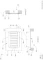
- FIG. 2shows a simplified schematic top view and an orthogonal cross-sectional view of a solidly-mounted transversely-excited film bulk acoustic resonator (SM XBAR) 200 .
- SM XBAR resonatorssuch as the resonator 200 may be used in a variety of RF filters including band-reject filters, band-pass filters, duplexers, and multiplexers.
- SM XBARsare particularly suited for use in filters for communications bands with frequencies above 3 GHz.
- the SM XBAR 200is made up of a thin film conductor pattern formed on a front surface 212 of a piezoelectric plate 210 having parallel front and back surfaces 212 , 214 , respectively.
- the piezoelectric plateis a thin single-crystal layer of a piezoelectric material such as lithium niobate, lithium tantalate, lanthanum gallium silicate, gallium nitride, or aluminum nitride.
- the piezoelectric plateis cut such that the orientation of the X, Y, and Z crystalline axes with respect to the front and back surfaces is known and consistent.
- the piezoelectric plate 210may be Z-cut, rotated Z-cut, or rotated Y-cut lithium niobate or lithium tantalate.
- SM XBARsmay be fabricated on piezoelectric plates with other crystallographic orientations.
- the back surface 214 of the piezoelectric plate 210is attached to, and mechanically supported by, a substrate 220 .
- the substrate 220may be, for example, silicon, sapphire, quartz, or some other material.
- the piezoelectric plate 210may be attached to the substrate 220 via a plurality of intermediate material layers.
- the conductor pattern of the SM XBAR 200includes an interdigital transducer (IDT) 230 .
- the IDT 230includes a first plurality of parallel fingers, such as finger 236 , extending from a first busbar 232 and a second plurality of fingers extending from a second busbar 234 .
- the first and second pluralities of parallel fingersare interleaved.
- the interleaved fingersoverlap for a distance AP, commonly referred to as the “aperture” of the IDT.
- the center-to-center distance L between the outermost fingers of the IDT 230is the “length” of the IDT.
- the first and second busbars 232 , 234serve as the terminals of the SM XBAR 200 .
- a radio frequency or microwave signal applied between the two busbars 232 , 234 of the IDT 230excites an acoustic wave within the piezoelectric plate 210 .
- the excited acoustic waveis a bulk shear wave that propagates in the direction normal to the surface of the piezoelectric plate 210 , which is also normal, or transverse, to the direction of the electric field created by the IDT fingers.
- the SM XBARis considered a transversely-excited film bulk wave resonator.
- the geometric pitch and width of the IDT fingersare greatly exaggerated with respect to the length (dimension L) and aperture (dimension AP) of the SM XBAR.
- a typical SM XBARhas more than ten parallel fingers in the IDT 210 .
- An SM XBARmay have hundreds, possibly thousands, of parallel fingers in the IDT 210 .
- the thickness of the fingers in the cross-sectional viewsis greatly exaggerated.
- FIG. 3shows a detailed schematic cross-sectional view of the SM XBAR 200 .
- the piezoelectric plate 210is a single-crystal layer of piezoelectrical material, as previously described, having a thickness tp.
- tpmay be, for example, 50 nm to 1500 nm.
- a front-side dielectric layer 314may optionally be formed on the front surface 212 of the piezoelectric plate 210 .
- the front-side dielectric layer 314has a thickness tfd.
- the front-side dielectric layer 314may be formed between the IDT fingers 236 a , 236 b .
- the front side dielectric layer 314may also be deposited over the IDT fingers 236 a , 236 b .
- the front-side dielectric layer 314may be a non-piezoelectric dielectric material, such as silicon dioxide or silicon nitride.
- tfdmay be, for example, 0 to not more than 30% of the thickness tp of the piezoelectric plate 210 .
- the IDT fingers 236 a , 236 bmay be aluminum or a substantially aluminum alloy, copper or a substantially copper alloy, beryllium, molybdenum, gold, or some other conductive material. Thin (relative to the total thickness of the conductors) layers of other metals, such as chromium or titanium, may be formed under and/or over the fingers to improve adhesion between the fingers and the piezoelectric plate 210 and/or to passivate or encapsulate the fingers.
- the busbars ( 232 , 234 in FIG. 2 ) of the IDTmay be made of the same or different materials as the fingers.
- the cross-sectional shape of the IDT fingersmay be trapezoidal (e.g. IDT finger 236 a ) or rectangular (e.g. IDT finger 236 b ), or some other shape (not shown).
- Dimension pis the center-to-center spacing or “pitch” of the IDT fingers, which may be referred to as the pitch of the IDT and/or the pitch of the SM XBAR.
- Dimension wis the width or “mark” of the IDT fingers.
- the IDT of an SM XBARdiffers substantially from the IDTs used in surface acoustic wave (SAW) resonators.
- SAWsurface acoustic wave
- the pitch of the IDTis one-half of the acoustic wavelength at the resonance frequency.
- the ratio of the finger width to the pitch of a SAW resonator IDTis typically close to 0.5 (i.e. the mark or finger width w is about one-fourth of the acoustic wavelength at resonance).
- the width w of the IDT fingersis typically 0.2 to 0.3 times the pitch p of the IDT.
- the center-to-center spacing of the IDT fingers and/or the width of the IDT fingersmay vary along the length of the IDT. For example, varying the center-to-center spacing and/or the width of the IDT fingers may suppress undesired spurious acoustic modes. In such cases, the dimensions p and w are defined to be the average value of the center-to-center spacing and width, respectively.
- the pitch p of the IDTmay be 2 to 20 times the thickness tp of the piezoelectric plate 210 .
- the pitch p of the IDTmay typically be 5 to 12.5 times tp.
- the thickness tm of the IDT fingers 236 a , 236 bis typically 0.8 to 1.5 times the thickness tp of the piezoelectric plate 210 .
- the thickness of the busbars ( 232 , 234 in FIG. 2 ) of the IDTmay be the same as, or greater than, the thickness tm of the IDT fingers.
- An acoustic Bragg reflector 340is sandwiched between a surface 222 of the substrate 220 and the back surface 214 of the piezoelectric plate 110 .
- the term “sandwiched”means the acoustic Bragg reflector 340 is both disposed between and physically connected to the surface 222 of the substrate 220 and the back surface 214 of the piezoelectric plate 210 .
- thin layers of additional materialsmay be disposed between the acoustic Bragg reflector 340 and the surface 222 of the substrate 220 and/or between the Bragg reflector 340 and the back surface 214 of the piezoelectric plate 210 .
- Such additional material layersmay be present, for example, to facilitate bonding the piezoelectric plate 210 , the acoustic Bragg reflector 340 , and the substrate 220 .
- the acoustic Bragg reflector 340includes multiple layers that alternate between materials having high acoustic impedance and materials have low acoustic impedance. “High” and “low” are relative terms. For each layer, the standard for comparison is the adjacent layers. Each “high” acoustic impedance layer has an acoustic impedance higher than that of both the adjacent low acoustic impedance layers. Each “low” acoustic impedance layer has an acoustic impedance lower than that of both the adjacent high acoustic impedance layers. Each of the layers has a thickness equal to, or about, one-fourth of the acoustic wavelength at or near a resonance frequency of the SM XBAR 200 . All of the high acoustic impedance layers of the acoustic Bragg reflector 340 are not necessarily the same material, and all of the low acoustic impedance layers are not necessarily the same material.
- Dielectric materials having comparatively low acoustic impedanceinclude silicon dioxide, silicon oxycarbide, and certain plastics such as cross-linked polyphenylene polymers.
- Dielectric materials having comparatively high acoustic impedanceinclude silicon nitride, aluminum nitride, silicon carbide, diamond, diamond-like carbon (DLC), cubic boron nitride (c-BN), and hafnium oxide.
- Aluminumhas comparatively low acoustic impedance and other metals such as molybdenum, tungsten, gold, and platinum have comparatively high acoustic impedance.
- the presence of metal layers in the acoustic Bragg reflector 340will distort the electric field generated by the IDT fingers and substantially reduce the electromechanical coupling of the SM XBAR.
- all of the layers of the acoustic Bragg reflector 340may be dielectric materials.
- the acoustic Bragg reflector 340has a total of six layers or three pairs of layers.
- An acoustic Bragg reflectormay have more than, or less than, six layers.
- FIG. 4is a graphical illustration of the primary acoustic mode in a SM XBAR 400 .
- FIG. 4shows a small portion of the SM XBAR 400 including a piezoelectric plate 410 and three interleaved IDT fingers 430 .
- the piezoelectric plate 410may be single-crystal lithium niobate cut such that the z-axis is normal to the surfaces of the plate.
- the IDT fingersmay be oriented parallel to the x-axis of the plate such that the y-axis is normal to the fingers.
- An RF voltage applied to the interleaved fingers 430creates a time-varying electric field between the fingers.
- the direction of the electric fieldis predominantly lateral, or parallel to the surface of the piezoelectric plate 410 , and orthogonal to the length of the IDT fingers, as indicated by the dashed arrows labeled “electric field”. Due to the high dielectric constant of the piezoelectric plate, the electric field is highly concentrated in the plate relative to the air. The lateral electric field excites acoustic waves in the piezoelectric plate 410 .
- the piezoelectric plate and the IDTare configured such that the lateral electric field causes shear deformation, and thus strongly excites shear-mode acoustic waves, in the piezoelectric plate 410 .
- shear deformationis defined as deformation in which parallel planes in a material remain parallel and maintain a constant distance while translating relative to each other.
- Shear acoustic wavesare defined as acoustic waves in a medium that result in shear deformation of the medium.
- the shear deformations in the piezoelectric plate 410are represented by the curves 460 , with the adjacent small arrows providing a schematic indication of the direction and magnitude of atomic motion.
- An acoustic Bragg reflector 440is sandwiched between the piezoelectric plate 410 and a substrate 420 .
- the acoustic Bragg reflector 440reflects the acoustic waves of the primary acoustic mode to keep the acoustic energy (arrow 465 ) predominantly confined to the piezoelectric plate 410 .
- the acoustic Bragg reflector 440 for an XBARconsists of alternating layers of materials having relatively high and relatively low acoustic impedance, with each layer having a thickness of about one-quarter of the wavelength of the shear acoustic waves (arrow 465 ) at resonance frequency of the XBAR 400 .
- the acoustic Bragg reflector 440has a total of six layers.
- An acoustic Bragg reflectormay have more than, or less than, six layers.
- FIG. 5is a schematic circuit diagram for a high frequency band-pass filter 500 using SM XBARs.
- the filter 500has a conventional ladder filter architecture including three series resonators 520 A, 520 B, 520 C and two shunt resonators 530 A, 530 B.
- the three series resonators 520 A, 520 B, 520 Care connected in series between a first port and a second port.
- the first and second portsare labeled “In” and “Out”, respectively.
- the filter 500is bidirectional and either port and serve as the input or output of the filter.
- the two shunt resonators 530 A, 530 Bare connected from nodes between the series resonators to ground.
- the architecture of the filter 500is commonly referred to as a “ladder filter circuit”. All the shunt resonators and series resonators of the filter 500 are SM XBARs. Although not shown in FIG. 5 , some or all of the resonators may be divided into multiple sub-resonators electrically connected in parallel.
- the filter 500may include a substrate having a surface, a single-crystal piezoelectric plate having front and back surfaces, and an acoustic Bragg reflector sandwiched between the surface of the substrate and the back surface of the piezoelectric plate.
- the substrate, acoustic Bragg reflector, and piezoelectric plateare represented by the rectangle 510 in FIG. 5 .
- a conductor pattern formed on the front surface of the single-crystal piezoelectric plateincludes interdigital transducers (IDTs) for each of the three series resonators 520 A, 520 B, 520 C and two shunt resonators 530 A, 530 B.
- the conductor patternincludes conductors to interconnect the resonators in the ladder filter circuit. All of the IDTs are configured to excite shear acoustic waves in the single-crystal piezoelectric plate in response to respective radio frequency signals applied to each IDT.
- the resonance frequencies of shunt resonatorsare typically lower than the resonance frequencies of series resonators.
- the resonance frequency of an SM XBAR resonatoris primarily determined by the thickness of the piezoelectric plate and dielectric layers, if present, above the acoustic Bragg reflector. Resonance frequency also determined, to a lesser extent, by IDT pitch and finger width. IDT pitch and finger width also impact other filter parameters including impedance and power handling capability. For broad-band filter applications, it may not be practical to provide the required difference between the resonance frequencies of shunt and series resonators using only differences in IDT pitch and/or finger width.
- a first dielectric layer(represented by the dashed rectangle 535 ) having a first thickness t 1 may be deposited over the IDTs of some or all of the shunt resonators 530 A, 530 B.
- a second dielectric layer(represented by the dashed rectangle 525 ) having a second thickness t 2 , less than t 1 , may be deposited over the IDTs of the series resonators 520 A, 520 B, 520 C.
- the second dielectric layermay be deposited over both the shunt and series resonators.
- the difference between the thickness t 1 and the thickness t 2defines a frequency offset between the series and shunt resonators.
- Individual series or shunt resonatorsmay be tuned to different frequencies by varying the pitch of the respective IDTs. In some filters, more than two dielectric layers of different thicknesses may be used as described in co-pending application Ser. No. 16/924,108.
- the shunt resonators 530 A, 530 Bmay be formed on portions of the piezoelectric plate having a thickness t 3 and the series resonators 520 A, 520 B, 520 Cv may be fabricated on portions of the piezoelectric plate having a thickness t 4 less than t 3 .
- the difference between the thicknesses t 3 and t 4defines a frequency offset between the series and shunt resonators.
- Individual series or shunt resonatorsmay be tuned to different frequencies by varying the pitch of the respective IDTs. In some filters, three or more different piezoelectric plate thicknesses may be used to provide additional frequency tuning capability.
- the filter 500is exemplary. Filters may contain more or fewer than five total resonators, more than two shunt resonators, and more or fewer than three series resonators. Filters may include shunt resonators connected from one or both of the input port and the output port to ground. Filters may contain additional reactive components, such as inductors and capacitors, not shown in FIG. 5
- FIG. 6is a plan view of an exemplary filter 600 which is an embodiment of the filter 500 of FIG. 5 .
- the filter 600includes five SM XBARs, represented by horizontally hashed rectangles, formed on a chip 610 .
- Series resonators 520 A, 520 B, 520 C and shunt resonator 530 A, 530 Bare identified by the reference designators from FIG. 5 .
- the chip 610includes an acoustic Bragg reflector sandwiched between a substrate and a piezoelectric plate. Only the surface of the piezoelectric plate is visible in FIG. 6 .
- the five SM XBARsare connected to each other and to circuitry external to the filter 600 by shaded conductors, such as conductors 632 and 634 .
- Labels “IN”, “OUT”, and “GND”represent contact pads for connections to the external circuitry. Areas of the chip 610 that are not hashed or shaded are the surface of the piezoelectric plate, which may be seen through one or more dielectric layers.
- the term “conductor pattern”refers to one or more patterned metal layers on the chip.
- the term “conductor”means an element of a conductor pattern other than IDT fingers.
- Conductorencompasses the busbars of the IDTs, pads for connection to circuitry external to the chip, and metal traces that connect the resonators and pads into a ladder filter circuit.
- a “signal conductor”carries an RF signal between resonators and/or the input and output pads.
- a “ground conductor”connects a ground pad to one or more shunt resonators.
- “Adjacent conductors”are pairs of conductors that face each other without any intervening elements on the surface of the piezoelectric plate. Inspection of FIG. 6 shows there are numerous pairs of adjacent conductors separated by only unshaded areas of the chip.
- conductor 632is a signal conductor that includes a busbar of series resonator 520 C and connects to the “OUT” pad of the filter.
- Conductor 634is ground conductor. The difference in potential between the RF signal on conductor 632 and ground (i.e., the signal at the output of the filter) imposes an electric field in the piezoelectric plate between the conductors 632 and 634 .
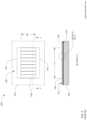
- FIG. 7is a detailed cross-sectional view of a portion of the filter 600 at a section plain E-E identified in FIG. 6 .
- the cross-sectional viewincludes the chip 610 and conductors 632 and 634 .
- the chip 610includes an acoustic Bragg reflector 740 sandwiched between a substrate 720 and a piezoelectric plate 710 .
- An optional dielectric layer 714may be over the conductors 632 , 634 and the surface of the piezoelectric plate 710 .
- signal conductor 632is a busbar of series resonator 520 C which connects to the “OUT” pad of the filter.
- Conductor 634is a grounded conductor. The difference in potential between the RF signal on signal conductor 632 (the signal output from the filter) and grounded conductor 634 imposes an electric field, represented by the arrow 790 , in the piezoelectric plate 710 between the conductors. The electric field will excite acoustic waves in the piezoelectric plate, including shear waves that travel substantially vertically. These shear waves will reflect from the acoustic Bragg reflector 740 and may resonate at a frequency within or near the pass-band of the filter 600 .
- the distance dm between the conductors 632 and 634will typically be an order of magnitude larger than the pitch p of any of the SM XBARs in the filter 600 .
- the amplitude of the acoustic waves excited between the conductors 632 and 634will be proportionally less than the amplitude of the acoustic waves within the SM XBARs.
- the smaller acoustic waves excited between the various conductors of the filter 600will incrementally increase the insertion loss in the filter pass-band and may cause objectionable ripple or spikes in the filter input/output transfer function in or near the filter pass-band.
- FIG. 8is another detailed cross-sectional view of a portion of a filter 800 .
- the filter 800may be the same as the filter 600 except that some of the piezoelectric material between conductors has been removed.
- FIG. 8shows a section plain E′-E′ which is at the same location in the filter 800 as the section plain E-E identified in FIG. 6 .
- the cross-sectional viewincludes the chip 610 and conductors 632 and 634 .
- the chip 610includes an acoustic Bragg reflector 740 sandwiched between a substrate 720 and a piezoelectric plate 810 .
- An optional dielectric layer 714may be over the conductors 632 , 634 and the surface of the piezoelectric plate 810 .
- the filter 800 shown in FIG. 8differs from the filter 600 of FIG. 7 in that a portion of the piezoelectric plate 810 between the conductor 632 and 634 has been removed, leaving an opening 850 through the piezoelectric plate 810 .
- the piezoelectric materialmay be removed, for example, by etching through a mask. Removing the piezoelectric material reduces or eliminates the problems caused by the excitation of undesired acoustic waves between the conductors 632 and 634 .
- the width dp of the opening 850is less than the distance dm between the conductors 632 , 634 . Acoustic waves will be excited in the remaining portions of the piezoelectric plate between the conductors 632 , 634 , but not in the opening where the piezoelectric material has been removed.
- the width dpis greater than or equal to 50% of the distance dm.
- the piezoelectric materialis removed between a signal conductor 632 and a ground conductor 634 .
- Piezoelectric materialmay also be removed between pairs of signal conductors where appropriate.
- FIG. 9is another detailed cross-sectional view of a portion of a filter 900 which may be the same as the filter 600 except that some of the piezoelectric material between conductors has been removed.
- FIG. 9shows a section plain E′′-E′′ which is at the same location in the filter 900 as the section plain E-E identified in FIG. 6 .
- the cross-sectional viewincludes the chip 610 and conductors 632 and 634 .
- the chip 610includes an acoustic Bragg reflector 740 sandwiched between a substrate 720 and a piezoelectric plate 910 .
- An optional dielectric layer 714may be over the conductors 632 , 634 and the surface of the piezoelectric plate 910 .
- the filter 900 shown in FIG. 9differs from the filter 800 of FIG. 8 in that the width dp of the opening 950 through the piezoelectric plate 910 (the area where the piezoelectric material has been removed) is greater than the distance dm between the conductors 632 , 634 .
- the opening 950extends under one or both of the conductors 632 , 634 .
- the piezoelectric materialmay be removed, for example, by etching through a mask prior to forming the conductors. Removing the piezoelectric material reduces or eliminates the problems caused by the excitation of undesired acoustic waves between the conductors 632 and 634 .
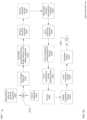
- FIG. 10is a simplified flow chart of a method 1000 for making a filter incorporating SM XBARs.
- the method 1000starts at 1010 with a piezoelectric film disposed on a sacrificial substrate 1002 and a device substrate 1004 .
- the method 1010ends at 1095 with a completed SM XBAR or filter.
- the flow chart of FIG. 10includes only major process steps. Various conventional process steps (e.g. surface preparation, cleaning, inspection, baking, annealing, monitoring, testing, etc.) may be performed before, between, after, and during the steps shown in FIG. 10 .
- Thin plates of single-crystal piezoelectric materials bonded to a non-piezoelectric substrateare commercially available. At the time of this application, both lithium niobate and lithium tantalate plates are available bonded to various substrates including silicon, quartz, and fused silica. Thin plates of other piezoelectric materials may be available now or in the future.
- the thickness of the piezoelectric platemay be between 50 nm and 1500 nm.
- the thickness of the piezoelectric plate at 1002may be equal to a desired final thickness. The thickness of the piezoelectric plate at 1002 may be greater than the final thickness and may be trimmed to the final thickness at a later step in the process 1000 .
- the piezoelectric plate 1002may be, for example, z-cut lithium niobate bonded to a silicon wafer with an intervening SiO 2 layer.
- the device substrate 1004may be silicon (as used in the previous examples) fused silica, quartz, or some other material.
- an acoustic Bragg reflectoris formed by depositing alternating layers of materials having low and high acoustic impedance as previously described. Each of the layers has a thickness equal to or about one-fourth of the acoustic wavelength. The total number of layers in the acoustic Bragg reflector may typically be from five to eight.
- all of the layers of the acoustic Bragg reflectormay be deposited on either the surface of the piezoelectric plate on the sacrificial substrate 1002 or a surface of the device substrate 1004 .
- some of the layers of the acoustic Bragg reflectormay be deposited on the surface of the piezoelectric plate on the sacrificial substrate 1002 and the remaining layers of the acoustic Bragg reflector may be deposited on a surface of the device substrate 1004 .
- the piezoelectric plate on the sacrificial substrate 1002 and the device substrate 1004may be bonded such that the layers of the acoustic Bragg reflector are sandwiched between the piezoelectric plate and the device substrate.
- the piezoelectric plate on the sacrificial substrate 1002 and the device substrate 1004may be bonded using a wafer bonding process such as direct bonding, surface-activated or plasma-activated bonding, electrostatic bonding, or some other bonding technique. Note that, when one or more layers of the acoustic Bragg reflector are deposited on both the piezoelectric plate and the device substrate, the bonding will occur between or within layers of the acoustic Bragg reflector.
- the sacrificial substrate, and any intervening layers,are removed at 1030 to expose the surface of the piezoelectric plate (the surface that previously faced the sacrificial substrate).
- the sacrificial substratemay be removed, for example, by material-dependent wet or dry etching or some other process.
- An alternative process 1000starts with a single-crystal piezoelectric wafer at 1002 instead of a thin piezoelectric plate on a sacrificial substrate of a different material. Ions are implanted to a controlled depth beneath a surface of the piezoelectric wafer (not shown in FIG. 10 ). The portion of the wafer from the surface to the depth of the ion implantation is (or will become) the thin piezoelectric plate and the balance of the wafer is the sacrificial substrate.
- the acoustic Bragg reflectoris formed at 1020 as previously described and the piezoelectric wafer and device substrate are bonded at 1025 such that the acoustic Bragg reflector is disposed between the ion-implanted surface of the piezoelectric wafer 1002 and the device substrate 1004 .
- the piezoelectric wafermay be split at the plane of the implanted ions (for example, using thermal shock), leaving a thin plate of piezoelectric material exposed and bonded to the acoustic Bragg reflector.
- the thickness of the thin plate piezoelectric materialis determined by the energy (and thus depth) of the implanted ions.
- the process of ion implantation and subsequent separation of a thin plateis commonly referred to as “ion slicing”.
- the thickness of the piezoelectric plate after ion slicingmay be equal to or greater than the desired final thickness.
- the exposed surface of the piezoelectric platemay be processed at 1035 .
- the surface of the piezoelectric platemay be polished or chemo-mechanically polished to remove damaged material, reduce surface roughness, and or reduce the thickness of the piezoelectric plate.
- a photoresist layermay be applied to the surface of the piezoelectric plate and patterned to form a mask that protects specific areas where resonators will be formed.
- the protected areasmay be as large or slightly larger than the areas of the IDTs of the resonators.
- the maskmay only unprotect selected areas between conductors.
- the unprotected portions of the piezoelectric platemay then be removed by a wet or dry etch.
- a lithium niobate piezoelectric platemay be etched by inductively coupled plasma reactive ion etching using argon and sulfur hexafluoride.
- a conductor patternincluding IDTs of each SM XBAR, is formed at 1045 by depositing and patterning one or more conductor layers on the trimmed surface of the piezoelectric plate.
- the conductor patternmay be, for example, aluminum, an aluminum alloy, copper, a copper alloy, or some other conductive metal.
- one or more layers of other materialsmay be disposed below (i.e. between the conductor layer and the piezoelectric plate) and/or on top of the conductor layer.
- a thin film of titanium, chrome, or other metalmay be used to improve the adhesion between the conductor layer and the piezoelectric plate.
- the IDT finger thicknessmay be from 0.10 to 1.5 times the final thickness of the piezoelectric plate.
- a conduction enhancement layer of gold, aluminum, copper or other higher conductivity metalmay be formed over portions of the conductor pattern (for example the IDT bus bars and interconnections between the IDTs).
- the conductor patternmay be formed at 1045 by depositing the conductor layer and, optionally, one or more other metal layers in sequence over the surface of the piezoelectric plate. The excess metal may then be removed by etching through patterned photoresist.
- the conductor layercan be etched, for example, by plasma etching, reactive ion etching, wet chemical etching, and other etching techniques.
- the conductor patternmay be formed at 1045 using a lift-off process.
- Photoresistmay be deposited over the piezoelectric plate. and patterned to define the conductor pattern.
- the conductor layer and, optionally, one or more other layersmay be deposited in sequence over the surface of the piezoelectric plate. The photoresist may then be removed, which removes the excess material, leaving the conductor pattern.
- the removal of selected portions of the piezoelectric plate at 1035may be performed after forming the conductor pattern(s) at 1045 .
- one or more frequency setting dielectric layer(s)optionally may be formed by depositing one or more layers of dielectric material on the front side of the piezoelectric plate.
- a dielectric layermay be formed over the shunt resonators to lower the frequencies of the shunt resonators relative to the frequencies of the series resonators.
- the one or more dielectric layersmay be deposited using a conventional deposition technique such as physical vapor deposition, atomic layer deposition, chemical vapor deposition, or some other method.
- One or more lithography processesmay be used to limit the deposition of the dielectric layers to selected areas of the piezoelectric plate.
- a maskmay be used to limit a dielectric layer to cover only the shunt resonators.
- a passivation/tuning dielectric layeris deposited over the piezoelectric plate and conductor patterns.
- the passivation/tuning dielectric layermay cover the entire surface of the filter except for pads for electrical connections to circuitry external to the filter.
- frequency tuningmay be performed by selectively adjusting the thickness of the passivation/tuning layer deposited over the resonators at 1055 .
- the frequency of a filter device pass-bandcan be lowered by adding material to the passivation/tuning layer, and the frequency of the filter device passband can be increased by removing material to the passivation/tuning layer.
- the process 1000is biased to produce filter devices with passbands that are initially lower than a required frequency range but can be tuned to the desired frequency range by removing material from the surface of the passivation/tuning layer.
- a probe card or other meansmay be used to make electrical connections with the filter to allow radio frequency (RF) tests and measurements of filter characteristics such as input-output transfer function.
- RF measurementsare made on all, or a large portion, of the filter devices fabricated simultaneously on a common piezoelectric plate and substrate.
- global frequency tuningmay be performed by removing material from the surface of the passivation/tuning layer using a selective material removal tool such as, for example, a scanning ion mill as previously described.
- a selective material removal toolsuch as, for example, a scanning ion mill as previously described.
- “Global” tuningis performed with a spatial resolution equal to or larger than an individual filter device. The objective of global tuning is to move the passband of each filter device towards a desired frequency range.
- the test results from 1060may be processed to generate a global contour map indicating the amount of material to be removed as a function of two-dimensional position on the wafer. The material is then removed in accordance with the contour map using the selective material removal tool.
- local frequency tuningmay be performed in addition to, or instead of, the global frequency tuning performed at 1065 .
- “Local” frequency tuningis performed with a spatial resolution smaller than an individual filter device.
- the test results from 1060may be processed to generate a map indicating the amount of material to be removed at each filter device.
- Local frequency tuningmay require the use of a mask to restrict the size of the areas from which material is removed. For example, a first mask may be used to restrict tuning to only shunt resonators, and a second mask may be subsequently used to restrict tuning to only series resonators (or vice versa). This would allow independent tuning of the lower band edge (by tuning shunt resonators) and upper band edge (by tuning series resonators) of the filter devices.
- the filter deviceis completed at 1075 .
- Actions that may occur at 1075include forming bonding pads or solder bumps or other means for making connection between the device and external circuitry (if such pads were not formed at 1045 ); excising individual filter devices from a wafer containing multiple filter devices; other packaging steps; and additional testing.
- the processends at 1095 .
- “plurality”means two or more. As used herein, a “set” of items may include one or more of such items.
- the terms “comprising”, “including”, “carrying”, “having”, “containing”, “involving”, and the likeare to be understood to be open-ended, i.e., to mean including but not limited to. Only the transitional phrases “consisting of” and “consisting essentially of”, respectively, are closed or semi-closed transitional phrases with respect to claims.
Landscapes
- Physics & Mathematics (AREA)
- Acoustics & Sound (AREA)
- Chemical & Material Sciences (AREA)
- Crystallography & Structural Chemistry (AREA)
- Piezo-Electric Or Mechanical Vibrators, Or Delay Or Filter Circuits (AREA)
Abstract
Description
Claims (22)
Priority Applications (2)
| Application Number | Priority Date | Filing Date | Title |
|---|---|---|---|
| US17/563,033US12255626B2 (en) | 2020-11-13 | 2021-12-27 | Solidly-mounted transversely-excited film bulk acoustic filters with excess piezoelectric material removed |
| US19/001,340US20250132748A1 (en) | 2020-11-13 | 2024-12-24 | Solidly-mounted transversely-excited film bulk acoustic filters with excess piezoelectric material removed |
Applications Claiming Priority (3)
| Application Number | Priority Date | Filing Date | Title |
|---|---|---|---|
| US202063113301P | 2020-11-13 | 2020-11-13 | |
| US17/123,029US11496113B2 (en) | 2020-11-13 | 2020-12-15 | XBAR devices with excess piezoelectric material removed |
| US17/563,033US12255626B2 (en) | 2020-11-13 | 2021-12-27 | Solidly-mounted transversely-excited film bulk acoustic filters with excess piezoelectric material removed |
Related Parent Applications (1)
| Application Number | Title | Priority Date | Filing Date |
|---|---|---|---|
| US17/123,029Continuation-In-PartUS11496113B2 (en) | 2020-11-13 | 2020-12-15 | XBAR devices with excess piezoelectric material removed |
Related Child Applications (1)
| Application Number | Title | Priority Date | Filing Date |
|---|---|---|---|
| US19/001,340ContinuationUS20250132748A1 (en) | 2020-11-13 | 2024-12-24 | Solidly-mounted transversely-excited film bulk acoustic filters with excess piezoelectric material removed |
Publications (2)
| Publication Number | Publication Date |
|---|---|
| US20220158622A1 US20220158622A1 (en) | 2022-05-19 |
| US12255626B2true US12255626B2 (en) | 2025-03-18 |
Family
ID=81588021
Family Applications (2)
| Application Number | Title | Priority Date | Filing Date |
|---|---|---|---|
| US17/563,033Active2042-06-26US12255626B2 (en) | 2020-11-13 | 2021-12-27 | Solidly-mounted transversely-excited film bulk acoustic filters with excess piezoelectric material removed |
| US19/001,340PendingUS20250132748A1 (en) | 2020-11-13 | 2024-12-24 | Solidly-mounted transversely-excited film bulk acoustic filters with excess piezoelectric material removed |
Family Applications After (1)
| Application Number | Title | Priority Date | Filing Date |
|---|---|---|---|
| US19/001,340PendingUS20250132748A1 (en) | 2020-11-13 | 2024-12-24 | Solidly-mounted transversely-excited film bulk acoustic filters with excess piezoelectric material removed |
Country Status (1)
| Country | Link |
|---|---|
| US (2) | US12255626B2 (en) |
Families Citing this family (1)
| Publication number | Priority date | Publication date | Assignee | Title |
|---|---|---|---|---|
| DE102023203135A1 (en)* | 2023-04-05 | 2024-10-10 | Robert Bosch Gesellschaft mit beschränkter Haftung | MEMS bulk wave resonator, a method for producing such a MEMS bulk wave resonator and a system with such a MEMS bulk wave resonator |
Citations (151)
| Publication number | Priority date | Publication date | Assignee | Title |
|---|---|---|---|---|
| US5204575A (en) | 1990-10-15 | 1993-04-20 | Kokusai Electric Co., Ltd. | Surface acoustic wave resonator |
| US5274345A (en) | 1992-05-13 | 1993-12-28 | Andersen Laboratories | Dual function reflector structures for interdigital saw transducer |
| US5446330A (en) | 1993-03-15 | 1995-08-29 | Matsushita Electric Industrial Co., Ltd. | Surface acoustic wave device having a lamination structure |
| US5552655A (en) | 1994-05-04 | 1996-09-03 | Trw Inc. | Low frequency mechanical resonator |
| US5726610A (en) | 1995-06-19 | 1998-03-10 | Motorola Inc. | Saw filter device for radio tranceiver utilizing different coupling coefficient ratios |
| US5729186A (en) | 1995-04-12 | 1998-03-17 | Matsushita Electric Industrial Co., Ltd. | Resonator ladder surface acoustic wave filter suppressing spurious signals |
| US5853601A (en) | 1997-04-03 | 1998-12-29 | Northrop Grumman Corporation | Top-via etch technique for forming dielectric membranes |
| US6172582B1 (en) | 1996-02-20 | 2001-01-09 | Cts Corporation | Saw resonator and ladder filter with specified number of reflector electrode fingers |
| US6271617B1 (en) | 1997-08-28 | 2001-08-07 | Murata Manufacturing Co., Ltd. | Surface acoustic wave device with a tungsten-aluminum layered interdigital transducer |
| US6377140B1 (en) | 1999-07-09 | 2002-04-23 | Oki Electric Industry Co., Ltd. | Saw resonator filter with bridged-T configuration |
| US20020079986A1 (en) | 2000-12-21 | 2002-06-27 | Ruby Richard C. | Bulk acoustic resonator perimeter reflection system |
| US20020130736A1 (en) | 2001-03-19 | 2002-09-19 | Murata Manufacturing Co., Ltd | Edge-reflection surface acoustic wave filter |
| US20020158714A1 (en) | 2001-04-27 | 2002-10-31 | Nokia Corporation | Method and system for wafer-level tuning of bulk acoustic wave resonators and filters by reducing thickness non-uniformity |
| US20020189062A1 (en) | 2001-06-15 | 2002-12-19 | Asia Pacific Microsystems, Inc. | Manufacturing method for a high quality film bulk acoustic wave device |
| US6516503B1 (en) | 1999-05-26 | 2003-02-11 | Murata Manufacturing Co., Ltd. | Method of making surface acoustic wave device |
| US20030042998A1 (en) | 2001-08-24 | 2003-03-06 | Edmonson Peter J. | Leaky surface acoustic wave resonators |
| US6540827B1 (en) | 1998-02-17 | 2003-04-01 | Trustees Of Columbia University In The City Of New York | Slicing of single-crystal films using ion implantation |
| US20030080831A1 (en) | 2001-10-25 | 2003-05-01 | Naumenko Natalya F. | Surface acoustic wave devices using optimized cuts of lithium niobate (LiNbO3) |
| US6570470B2 (en) | 2000-06-30 | 2003-05-27 | Kyocera Corporation | Surface acoustic wave ladder filter utilizing parallel resonators with different resonant frequencies |
| US20030199105A1 (en) | 2002-04-22 | 2003-10-23 | Kub Francis J. | Method for making piezoelectric resonator and surface acoustic wave device using hydrogen implant layer splitting |
| US20040041496A1 (en) | 2002-09-04 | 2004-03-04 | Fujitsu Media Devices Limited | Surface acoustic wave device, filter device and method of producing the surface acoustic wave device |
| US6707229B1 (en) | 1999-06-03 | 2004-03-16 | Tele Filter Zweigniederlassung Der Dover Germany Gmbh | Surface acoustic wave filter |
| US20040100164A1 (en) | 2002-11-26 | 2004-05-27 | Murata Manufacturing Co., Ltd. | Manufacturing method of electronic device |
| US6833774B2 (en) | 2002-06-25 | 2004-12-21 | Sawtek, Inc. | Surface acoustic wave filter |
| US20040261250A1 (en) | 2000-09-06 | 2004-12-30 | Murata Manufacturing Co., Ltd. | Method for adjusting a frequency characteristic of an edge reflection type surface acoustic wave device and method for producing an- edge reflection type surface acoustic wave device |
| US20050077982A1 (en) | 2003-08-29 | 2005-04-14 | Tsukasa Funasaka | Surface acoustic wave element and electronic equipment provided with the element |
| US20050185026A1 (en) | 2004-01-26 | 2005-08-25 | Motohisa Noguchi | Piezoelectric element, piezoelectric actuator, ink jet recording head, ink jet printer, surface acoustic wave element, frequency filter, oscillator, electronic circuit, thin film piezoelectric resonator, and electronic apparatus |
| US20050218488A1 (en) | 2004-03-31 | 2005-10-06 | Mie Matsuo | Electronic component having micro-electrical mechanical system |
| US20050264136A1 (en) | 2004-05-31 | 2005-12-01 | Jun Tsutsumi | Surface acoustic wave device |
| US7009468B2 (en) | 2001-04-27 | 2006-03-07 | Murata Manufacturing Co., Ltd. | Surface acoustic wave device and electronic device using the same |
| US20060152107A1 (en) | 2005-01-07 | 2006-07-13 | Seiko Epson Corporation | Lamb-wave high-frequency resonator |
| US20060179642A1 (en) | 2005-02-03 | 2006-08-17 | Kabushiki Kaisha Toshiba | Method for manufacturing a film bulk acoustic resonator |
| US7105980B2 (en) | 2002-07-03 | 2006-09-12 | Sawtek, Inc. | Saw filter device and method employing normal temperature bonding for producing desirable filter production and performance characteristics |
| US20070182510A1 (en) | 2006-02-06 | 2007-08-09 | Samsung Electronics Co., Ltd. | Multi-band filter module and method of fabricating the same |
| US20070188047A1 (en) | 2006-02-16 | 2007-08-16 | Seiko Epson Corporation | Lamb wave type frequency device and method thereof |
| US20070194863A1 (en) | 2006-02-17 | 2007-08-23 | Kabushiki Kaisha Toshiba | Film bulk acoustic resonator and method of manufacturing same |
| US20070267942A1 (en) | 2006-05-19 | 2007-11-22 | Hisanori Matsumoto | Piezoelectric film resonator, radio-frequency filter using them, and radio-frequency module using them |
| US7345400B2 (en) | 2003-01-27 | 2008-03-18 | Murata Manufacturing Co., Ltd. | Surface acoustic wave device |
| US20080246559A1 (en) | 2007-01-19 | 2008-10-09 | Farrokh Ayazi | Lithographically-defined multi-standard multi-frequency high-Q tunable micromechanical resonators |
| US7463118B2 (en) | 2006-06-09 | 2008-12-09 | Texas Instruments Incorporated | Piezoelectric resonator with an efficient all-dielectric Bragg reflector |
| US7535152B2 (en) | 2005-10-19 | 2009-05-19 | Murata Manufacturing Co., Ltd. | Lamb wave device |
| US20100019866A1 (en) | 2008-07-23 | 2010-01-28 | Fujitsu Limited | Acoustic wave device, method of manufacturing acoustic wave device and transmission apparatus |
| US7684109B2 (en) | 2007-02-28 | 2010-03-23 | Maxim Integrated Products, Inc. | Bragg mirror optimized for shear waves |
| US20100123367A1 (en) | 2008-11-19 | 2010-05-20 | Ngk Insulators, Ltd. | Lamb wave device |
| US7868519B2 (en) | 2007-09-06 | 2011-01-11 | Murata Manufacturing Co., Ltd. | Piezoelectric resonator including an acoustic reflector portion |
| US20110018654A1 (en) | 2009-07-27 | 2011-01-27 | Avago Technologies Wireless Ip (Singapore) Pte. Ltd. | Resonator filter with multiple cross-couplings |
| US20110018389A1 (en) | 2008-01-30 | 2011-01-27 | Kyocera Corporation | Acoustic Wave Device and Method for Production of Same |
| US7941103B2 (en) | 2005-11-15 | 2011-05-10 | Taiyo Yuden Co., Ltd. | Duplexer |
| US20110109196A1 (en) | 2008-07-11 | 2011-05-12 | Goto Rei | Plate wave element and electronic equipment using same |
| US20110278993A1 (en) | 2010-05-17 | 2011-11-17 | Murata Manufacturing Co., Ltd. | Method for manufacturing composite piezoelectric substrate and piezoelectric device |
| US20120073390A1 (en) | 2010-09-29 | 2012-03-29 | The George Washington University | Synchronous One-Pole Surface Acoustic Wave Resonator |
| US8278802B1 (en) | 2008-04-24 | 2012-10-02 | Rf Micro Devices, Inc. | Planarized sacrificial layer for MEMS fabrication |
| US8294330B1 (en) | 2009-03-31 | 2012-10-23 | Triquint Semiconductor, Inc. | High coupling, low loss saw filter and associated method |
| US20120274416A1 (en)* | 2011-04-27 | 2012-11-01 | Taiyo Yuden Co., Ltd. | Ladder filter, duplexer and module |
| US20120286900A1 (en) | 2010-01-28 | 2012-11-15 | Murata Manufacturing Co., Ltd. | Tunable filter |
| US20120326809A1 (en) | 2010-03-12 | 2012-12-27 | Murata Manufacturing Co., Ltd. | Elastic wave resonator and ladder filter |
| US8344815B2 (en) | 2008-10-24 | 2013-01-01 | Seiko Epson Corporation | Surface acoustic wave resonator, surface acoustic wave oscillator, and surface acoustic wave module unit |
| US20130127551A1 (en) | 2010-08-05 | 2013-05-23 | Adaptalog Limited | Crystal reference oscillator for navigation applications |
| US20130234805A1 (en) | 2012-03-07 | 2013-09-12 | Taiyo Yuden Co., Ltd. | Resonator, frequency filter, duplexer, electronic device, and method of manufacturing resonator |
| US20130271238A1 (en) | 2012-04-13 | 2013-10-17 | Taiyo Yuden Co., Ltd. | Filter device, manufacturing method for filter device, and duplexer |
| US20130278609A1 (en) | 2012-04-19 | 2013-10-24 | Qualcomm Mems Technologies, Inc. | Isotropically-etched cavities for evanescent-mode electromagnetic-wave cavity resonators |
| US20130321100A1 (en) | 2012-06-05 | 2013-12-05 | Avago Technologies Wireless Ip (Singapore) Pte. Ltd. | Laterally-coupled acoustic resonators |
| US20140009032A1 (en) | 2012-07-04 | 2014-01-09 | Taiyo Yuden Co., Ltd. | Lamb wave device and manufacturing method thereof |
| US20140130319A1 (en) | 2010-09-28 | 2014-05-15 | Murata Manufacturing Co., Ltd. | Method for manufacturing piezoelectric device |
| US20140145556A1 (en) | 2011-08-08 | 2014-05-29 | Murata Manufacturing Co., Ltd. | Elastic wave device |
| US20140151151A1 (en) | 2010-10-15 | 2014-06-05 | Commissariat A L'energie Atomique Et Aux Energies Alternatives | Heterogenous acoustic structure formed from a homogeneous material |
| US20140152145A1 (en) | 2010-11-30 | 2014-06-05 | Murata Manufacturing Co., Ltd. | Elastic wave device and manufacturing method for same |
| US20140173862A1 (en) | 2007-12-25 | 2014-06-26 | Murata Manufacturing Co., Ltd. | Method for manufacturing composite piezoelectric substrate |
| US20140225684A1 (en) | 2011-10-24 | 2014-08-14 | Murata Manufacturing Co., Ltd. | Surface acoustic wave device |
| US8816567B2 (en) | 2011-07-19 | 2014-08-26 | Qualcomm Mems Technologies, Inc. | Piezoelectric laterally vibrating resonator structure geometries for spurious frequency suppression |
| US8829766B2 (en) | 2008-08-01 | 2014-09-09 | Epcos Ag | Piezoelectric resonator operating in thickness shear mode |
| US8932686B2 (en) | 2008-10-31 | 2015-01-13 | Murata Manufacturing Co., Ltd. | Method for producing piezoelectric composite substrate |
| US20150042417A1 (en) | 2013-08-06 | 2015-02-12 | Murata Manufacturing Co., Ltd. | High-frequency module |
| US20150165479A1 (en) | 2013-12-12 | 2015-06-18 | Qualcomm Incorporated | Piezoelectric ultrasonic transducer and process |
| US9130145B2 (en) | 2012-03-29 | 2015-09-08 | Vectron International Gmbh | Surface acoustic wave component |
| US9148121B2 (en) | 2012-08-17 | 2015-09-29 | Taiyo Yuden Co., Ltd. | Acoustic wave filter, duplexer, and module |
| US20150319537A1 (en) | 2012-12-12 | 2015-11-05 | Epcos Ag | Electroacoustic Components and Methods Thereof |
| US20150333730A1 (en) | 2010-04-23 | 2015-11-19 | Teknologian Tutkimuskeskus Vtt Oy | Wide-band acoustically coupled thin-film BAW filter |
| US20150365067A1 (en) | 2013-03-21 | 2015-12-17 | Ngk Insulators, Ltd. | Composite Substrates for Acoustic Wave Elements, and Acoustic Wave Elements |
| US9219466B2 (en) | 2011-11-11 | 2015-12-22 | Teknologian Tutkimuskeskus Vtt Oy | Laterally coupled bulk acoustic wave filter with improved passband characteristics |
| US20160028367A1 (en) | 2014-07-25 | 2016-01-28 | Akoustis, Inc. | Single crystal acoustic resonator and bulk acoustic wave filter |
| WO2016017104A1 (en) | 2014-07-31 | 2016-02-04 | Skyworks Panasonic Filter Solutions Japan Co., Ltd. | Acoustic wave filters and duplexers using same |
| US9276557B1 (en) | 2013-07-01 | 2016-03-01 | Sandia Corporation | Programmable electroacoustic filter apparatus and method for its manufacture |
| US20160087187A1 (en) | 2014-05-29 | 2016-03-24 | Avago Technologies General Ip (Singapore) Pte. Ltd. | Capacitive coupled resonator and filter device with comb electrodes and support pillars separating piezoelectric layer |
| US9369105B1 (en) | 2007-08-31 | 2016-06-14 | Rf Micro Devices, Inc. | Method for manufacturing a vibrating MEMS circuit |
| US20160182009A1 (en) | 2014-12-17 | 2016-06-23 | Rf Micro Devices, Inc. | Plate wave devices with wave confinement structures and fabrication methods |
| US9425765B2 (en) | 2013-04-22 | 2016-08-23 | Northeastern University | Nano- and micro-electromechanical resonators |
| US9525398B1 (en) | 2014-05-27 | 2016-12-20 | Sandia Corporation | Single crystal micromechanical resonator and fabrication methods thereof |
| US20170063332A1 (en) | 2015-08-25 | 2017-03-02 | Avago Technologies General Ip (Singapore) Pte. Ltd. | Surface acoustic wave (saw) resonator having trap-rich region |
| US9640750B2 (en) | 2011-03-25 | 2017-05-02 | Skyworks Filter Solutions Japan Co., Ltd. | Acoustic wave device with suppressed higher order transverse modes |
| US20170179928A1 (en) | 2015-11-13 | 2017-06-22 | Resonant Inc. | Acoustic wave filter with enhanced rejection |
| US20170179225A1 (en) | 2011-05-25 | 2017-06-22 | Semiconductor Components Industries, Llc | Semiconductor device having a super junction structure and method of manufacturing the same |
| US20170214387A1 (en) | 2016-01-26 | 2017-07-27 | Avago Technologies General Ip (Singapore) Pte. Ltd. | Bulk acoustic wave resonator with piezoelectric layer comprising lithium niobate or lithium tantalate |
| US20170214381A1 (en) | 2016-01-22 | 2017-07-27 | Rf Micro Devices, Inc. | Guided wave devices with selectively thinned piezoelectric layers |
| US20170222617A1 (en) | 2014-10-16 | 2017-08-03 | Murata Manufacturing Co., Ltd. | High-frequency module |
| US20170222622A1 (en) | 2016-01-28 | 2017-08-03 | Triquint Semiconductor, Inc. | Surface acoustic wave device having a piezoelectric layer on a quartz substrate and methods of manufacturing thereof |
| US9762202B2 (en) | 2008-12-17 | 2017-09-12 | Analog Devices, Inc. | Method of manufacturing a mechanical resonating structure |
| US9780759B2 (en) | 2010-12-24 | 2017-10-03 | Murata Manufacturing Co., Ltd. | Elastic wave device and method for manufacturing the same |
| US9837984B2 (en) | 2014-12-24 | 2017-12-05 | Qorvo Us, Inc. | RF ladder filter with simplified acoustic RF resonator parallel capacitance compensation |
| US20170370791A1 (en) | 2016-06-28 | 2017-12-28 | Taiyo Yuden Co., Ltd. | Method of fabricating acoustic wave device and acoustic wave device |
| US20180005950A1 (en) | 2016-06-29 | 2018-01-04 | Murata Manufacturing Co., Ltd. | Electronic component device, method of mounting electronic component device on circuit board, and mounting structure of electronic component device on circuit board |
| WO2018003273A1 (en) | 2016-06-28 | 2018-01-04 | 株式会社村田製作所 | Multiplexer, high-frequency front end circuit, and communication device |
| US20180026603A1 (en) | 2015-05-22 | 2018-01-25 | Murata Manufacturing Co., Ltd. | Electronic component |
| US20180033952A1 (en) | 2016-07-28 | 2018-02-01 | Taiyo Yuden Co., Ltd. | Electronic device and method of fabricating the same |
| US20180041191A1 (en) | 2016-08-08 | 2018-02-08 | Samsung Electro-Mechanics Co., Ltd. | Saw filter device and method of manufacturing the same |
| US20180062617A1 (en) | 2016-08-25 | 2018-03-01 | Qualcomm Incorporated | Single-chip multi-frequency film bulk acoustic-wave resonators |
| US20180062615A1 (en) | 2015-05-08 | 2018-03-01 | Murata Manufacturing Co., Ltd. | High frequency module |
| US20180123016A1 (en) | 2012-06-15 | 2018-05-03 | Carnegie Mellon University | Microelectronic structures with suspended lithium-based thin films |
| US20180191322A1 (en) | 2017-01-03 | 2018-07-05 | Win Semiconductors Corp. | Method for fabricating bulk acoustic wave resonator with mass adjustment structure |
| US10079414B2 (en) | 2015-03-17 | 2018-09-18 | The United States Of America, As Represented By The Secretary Of The Navy | Switched multiplexer with flat group delay and channelized limiting |
| US20180278227A1 (en) | 2017-03-24 | 2018-09-27 | Dror Hurwitz | Method for fabricating rf resonators and filters |
| US10187039B2 (en) | 2016-06-07 | 2019-01-22 | Skyworks Filter Solutions Japan Co., Ltd. | Filter devices having reduced spurious emissions from lamb waves |
| US10200013B2 (en) | 2016-02-18 | 2019-02-05 | X-Celeprint Limited | Micro-transfer-printed acoustic wave filter device |
| US20190068164A1 (en) | 2016-03-11 | 2019-02-28 | Akoustis, Inc. | 5G BAND n79 ACOUSTIC WAVE RESONATOR RF FILTER CIRCUIT |
| US20190131953A1 (en) | 2017-10-31 | 2019-05-02 | The Board Of Trustees Of The University Of Illinois | Interdigital transducers on a piezoelectric thin-film for signal compression |
| US10284176B1 (en) | 2015-06-03 | 2019-05-07 | Qorvo Us, Inc. | Temperature compensated surface acoustic wave device and methods of manufacturing the same |
| US20190273480A1 (en) | 2018-03-02 | 2019-09-05 | Skyworks Solutions, Inc. | Lamb wave loop circuit for acoustic wave filter |
| US20190348966A1 (en) | 2018-05-10 | 2019-11-14 | Globalfoundries Singapore Pte. Ltd. | Acoustic wave filter formed on a v-groove topography and method for producing the same |
| US10491192B1 (en) | 2018-06-15 | 2019-11-26 | Resonant Inc. | Transversely-excited film bulk acoustic resonator |
| US20190379351A1 (en) | 2017-03-13 | 2019-12-12 | Murata Manufacturing Co., Ltd. | Notch filter |
| US20190386636A1 (en) | 2018-06-15 | 2019-12-19 | Resonant Inc. | Transversely-excited film bulk acoustic resonator |
| US20200007110A1 (en) | 2017-03-15 | 2020-01-02 | Murata Manufacturing Co., Ltd. | Acoustic wave element, acoustic wave filter device, and multiplexer |
| US20200021272A1 (en) | 2018-07-10 | 2020-01-16 | Texas Instruments Incorporated | Laterally Vibrating Bulk Acoustic Wave Resonator |
| US20200036357A1 (en) | 2017-04-26 | 2020-01-30 | Murata Manufacturing Co., Ltd. | Acoustic wave device |
| US10601392B2 (en) | 2018-06-15 | 2020-03-24 | Resonant Inc. | Solidly-mounted transversely-excited film bulk acoustic resonator |
| US10637438B2 (en) | 2018-06-15 | 2020-04-28 | Resonant Inc. | Transversely-excited film bulk acoustic resonators for high power applications |
| US20200235719A1 (en) | 2018-06-15 | 2020-07-23 | Resonant Inc. | Xbar resonators with non-rectangular diaphragms |
| US20200259480A1 (en) | 2019-02-08 | 2020-08-13 | Vtt Technical Research Centre Of Finland Ltd | Low loss acoustic device |
| US10790802B2 (en) | 2018-06-15 | 2020-09-29 | Resonant Inc. | Transversely excited film bulk acoustic resonator using rotated Y-X cut lithium niobate |
| US20200313645A1 (en) | 2019-03-25 | 2020-10-01 | Skyworks Solutions, Inc. | Acoustic wave filters with isolation |
| US10797675B2 (en) | 2018-06-15 | 2020-10-06 | Resonant Inc. | Transversely excited film bulk acoustic resonator using rotated z-cut lithium niobate |
| US10812048B2 (en) | 2016-09-02 | 2020-10-20 | Murata Manufacturing Co., Ltd. | Acoustic wave filter device, radio-frequency front-end circuit, and communication apparatus |
| US10819309B1 (en) | 2019-04-05 | 2020-10-27 | Resonant Inc. | Transversely-excited film bulk acoustic resonator package and method |
| US10826462B2 (en) | 2018-06-15 | 2020-11-03 | Resonant Inc. | Transversely-excited film bulk acoustic resonators with molybdenum conductors |
| US20200350891A1 (en) | 2018-06-15 | 2020-11-05 | Resonant Inc. | Transversely-excited film bulk acoustic resonator with etch-stop layer |
| US10868513B2 (en) | 2018-06-15 | 2020-12-15 | Resonant Inc. | Transversely-excited film bulk acoustic filters with symmetric layout |
| US10868510B2 (en) | 2018-06-15 | 2020-12-15 | Resonant Inc. | Transversely-excited film bulk acoustic resonator with half-lambda dielectric layer |
| US20210013859A1 (en) | 2018-06-15 | 2021-01-14 | Resonant Inc. | Transversely-excited film bulk acoustic resonator with etched conductor patterns |
| US10911021B2 (en) | 2019-06-27 | 2021-02-02 | Resonant Inc. | Transversely-excited film bulk acoustic resonator with lateral etch stop |
| US10917072B2 (en) | 2019-06-24 | 2021-02-09 | Resonant Inc. | Split ladder acoustic wave filters |
| US10985728B2 (en) | 2018-06-15 | 2021-04-20 | Resonant Inc. | Transversely-excited film bulk acoustic resonator and filter with a uniform-thickness dielectric overlayer |
| US10992284B2 (en) | 2018-06-15 | 2021-04-27 | Resonant Inc. | Filter using transversely-excited film bulk acoustic resonators with multiple frequency setting layers |
| US10992282B1 (en) | 2020-06-18 | 2021-04-27 | Resonant Inc. | Transversely-excited film bulk acoustic resonators with electrodes having a second layer of variable width |
| US10992283B2 (en) | 2018-06-15 | 2021-04-27 | Resonant Inc. | High power transversely-excited film bulk acoustic resonators on rotated Z-cut lithium niobate |
| US10998877B2 (en) | 2018-06-15 | 2021-05-04 | Resonant Inc. | Film bulk acoustic resonator fabrication method with frequency trimming based on electric measurements prior to cavity etch |
| US11003971B2 (en) | 2017-11-07 | 2021-05-11 | Resonant Inc. | Ultra-wide-band saw sensor with hyperbolically frequency-modulated etched reflector |
| US11146238B2 (en) | 2018-06-15 | 2021-10-12 | Resonant Inc. | Film bulk acoustic resonator fabrication method |
| US11146232B2 (en) | 2018-06-15 | 2021-10-12 | Resonant Inc. | Transversely-excited film bulk acoustic resonator with reduced spurious modes |
| US11143561B2 (en) | 2018-12-05 | 2021-10-12 | Resonant Inc. | Passive microphone/pressure sensor using a piezoelectric diaphragm |
| US20210328574A1 (en) | 2020-04-20 | 2021-10-21 | Resonant Inc. | Small transversely-excited film bulk acoustic resonators with enhanced q-factor |
| US11171629B2 (en) | 2018-06-15 | 2021-11-09 | Resonant Inc. | Transversely-excited film bulk acoustic resonator using pre-formed cavities |
- 2021
- 2021-12-27USUS17/563,033patent/US12255626B2/enactiveActive
- 2024
- 2024-12-24USUS19/001,340patent/US20250132748A1/enactivePending
Patent Citations (176)
| Publication number | Priority date | Publication date | Assignee | Title |
|---|---|---|---|---|
| US5204575A (en) | 1990-10-15 | 1993-04-20 | Kokusai Electric Co., Ltd. | Surface acoustic wave resonator |
| US5274345A (en) | 1992-05-13 | 1993-12-28 | Andersen Laboratories | Dual function reflector structures for interdigital saw transducer |
| US5446330A (en) | 1993-03-15 | 1995-08-29 | Matsushita Electric Industrial Co., Ltd. | Surface acoustic wave device having a lamination structure |
| US5552655A (en) | 1994-05-04 | 1996-09-03 | Trw Inc. | Low frequency mechanical resonator |
| US5729186A (en) | 1995-04-12 | 1998-03-17 | Matsushita Electric Industrial Co., Ltd. | Resonator ladder surface acoustic wave filter suppressing spurious signals |
| US5726610A (en) | 1995-06-19 | 1998-03-10 | Motorola Inc. | Saw filter device for radio tranceiver utilizing different coupling coefficient ratios |
| US6172582B1 (en) | 1996-02-20 | 2001-01-09 | Cts Corporation | Saw resonator and ladder filter with specified number of reflector electrode fingers |
| US5853601A (en) | 1997-04-03 | 1998-12-29 | Northrop Grumman Corporation | Top-via etch technique for forming dielectric membranes |
| US6271617B1 (en) | 1997-08-28 | 2001-08-07 | Murata Manufacturing Co., Ltd. | Surface acoustic wave device with a tungsten-aluminum layered interdigital transducer |
| US6540827B1 (en) | 1998-02-17 | 2003-04-01 | Trustees Of Columbia University In The City Of New York | Slicing of single-crystal films using ion implantation |
| US6710514B2 (en) | 1999-05-26 | 2004-03-23 | Murata Manufacturing Co., Ltd. | Surface acoustic wave device |
| US6516503B1 (en) | 1999-05-26 | 2003-02-11 | Murata Manufacturing Co., Ltd. | Method of making surface acoustic wave device |
| US6707229B1 (en) | 1999-06-03 | 2004-03-16 | Tele Filter Zweigniederlassung Der Dover Germany Gmbh | Surface acoustic wave filter |
| US6377140B1 (en) | 1999-07-09 | 2002-04-23 | Oki Electric Industry Co., Ltd. | Saw resonator filter with bridged-T configuration |
| US6570470B2 (en) | 2000-06-30 | 2003-05-27 | Kyocera Corporation | Surface acoustic wave ladder filter utilizing parallel resonators with different resonant frequencies |
| US20040261250A1 (en) | 2000-09-06 | 2004-12-30 | Murata Manufacturing Co., Ltd. | Method for adjusting a frequency characteristic of an edge reflection type surface acoustic wave device and method for producing an- edge reflection type surface acoustic wave device |
| US20020079986A1 (en) | 2000-12-21 | 2002-06-27 | Ruby Richard C. | Bulk acoustic resonator perimeter reflection system |
| US20020130736A1 (en) | 2001-03-19 | 2002-09-19 | Murata Manufacturing Co., Ltd | Edge-reflection surface acoustic wave filter |
| US20020158714A1 (en) | 2001-04-27 | 2002-10-31 | Nokia Corporation | Method and system for wafer-level tuning of bulk acoustic wave resonators and filters by reducing thickness non-uniformity |
| US7009468B2 (en) | 2001-04-27 | 2006-03-07 | Murata Manufacturing Co., Ltd. | Surface acoustic wave device and electronic device using the same |
| US20020189062A1 (en) | 2001-06-15 | 2002-12-19 | Asia Pacific Microsystems, Inc. | Manufacturing method for a high quality film bulk acoustic wave device |
| US20030042998A1 (en) | 2001-08-24 | 2003-03-06 | Edmonson Peter J. | Leaky surface acoustic wave resonators |
| US20030080831A1 (en) | 2001-10-25 | 2003-05-01 | Naumenko Natalya F. | Surface acoustic wave devices using optimized cuts of lithium niobate (LiNbO3) |
| US20030199105A1 (en) | 2002-04-22 | 2003-10-23 | Kub Francis J. | Method for making piezoelectric resonator and surface acoustic wave device using hydrogen implant layer splitting |
| US6833774B2 (en) | 2002-06-25 | 2004-12-21 | Sawtek, Inc. | Surface acoustic wave filter |
| US7105980B2 (en) | 2002-07-03 | 2006-09-12 | Sawtek, Inc. | Saw filter device and method employing normal temperature bonding for producing desirable filter production and performance characteristics |
| US20040041496A1 (en) | 2002-09-04 | 2004-03-04 | Fujitsu Media Devices Limited | Surface acoustic wave device, filter device and method of producing the surface acoustic wave device |
| US20040100164A1 (en) | 2002-11-26 | 2004-05-27 | Murata Manufacturing Co., Ltd. | Manufacturing method of electronic device |
| US7345400B2 (en) | 2003-01-27 | 2008-03-18 | Murata Manufacturing Co., Ltd. | Surface acoustic wave device |
| US20050077982A1 (en) | 2003-08-29 | 2005-04-14 | Tsukasa Funasaka | Surface acoustic wave element and electronic equipment provided with the element |
| US20050185026A1 (en) | 2004-01-26 | 2005-08-25 | Motohisa Noguchi | Piezoelectric element, piezoelectric actuator, ink jet recording head, ink jet printer, surface acoustic wave element, frequency filter, oscillator, electronic circuit, thin film piezoelectric resonator, and electronic apparatus |
| US20050218488A1 (en) | 2004-03-31 | 2005-10-06 | Mie Matsuo | Electronic component having micro-electrical mechanical system |
| US20050264136A1 (en) | 2004-05-31 | 2005-12-01 | Jun Tsutsumi | Surface acoustic wave device |
| US20060152107A1 (en) | 2005-01-07 | 2006-07-13 | Seiko Epson Corporation | Lamb-wave high-frequency resonator |
| US20060179642A1 (en) | 2005-02-03 | 2006-08-17 | Kabushiki Kaisha Toshiba | Method for manufacturing a film bulk acoustic resonator |
| US7535152B2 (en) | 2005-10-19 | 2009-05-19 | Murata Manufacturing Co., Ltd. | Lamb wave device |
| US7941103B2 (en) | 2005-11-15 | 2011-05-10 | Taiyo Yuden Co., Ltd. | Duplexer |
| US20070182510A1 (en) | 2006-02-06 | 2007-08-09 | Samsung Electronics Co., Ltd. | Multi-band filter module and method of fabricating the same |
| US20100064492A1 (en) | 2006-02-16 | 2010-03-18 | Seiko Epson Corporation | Lamb wave type frequency device and method thereof |
| US20070188047A1 (en) | 2006-02-16 | 2007-08-16 | Seiko Epson Corporation | Lamb wave type frequency device and method thereof |
| US7728483B2 (en) | 2006-02-16 | 2010-06-01 | Seiko Epson Corporation | Lamb wave type frequency device and method thereof |
| US20070194863A1 (en) | 2006-02-17 | 2007-08-23 | Kabushiki Kaisha Toshiba | Film bulk acoustic resonator and method of manufacturing same |
| US20070267942A1 (en) | 2006-05-19 | 2007-11-22 | Hisanori Matsumoto | Piezoelectric film resonator, radio-frequency filter using them, and radio-frequency module using them |
| US7463118B2 (en) | 2006-06-09 | 2008-12-09 | Texas Instruments Incorporated | Piezoelectric resonator with an efficient all-dielectric Bragg reflector |
| US20080246559A1 (en) | 2007-01-19 | 2008-10-09 | Farrokh Ayazi | Lithographically-defined multi-standard multi-frequency high-Q tunable micromechanical resonators |
| US7684109B2 (en) | 2007-02-28 | 2010-03-23 | Maxim Integrated Products, Inc. | Bragg mirror optimized for shear waves |
| US9369105B1 (en) | 2007-08-31 | 2016-06-14 | Rf Micro Devices, Inc. | Method for manufacturing a vibrating MEMS circuit |
| US7868519B2 (en) | 2007-09-06 | 2011-01-11 | Murata Manufacturing Co., Ltd. | Piezoelectric resonator including an acoustic reflector portion |
| US20140173862A1 (en) | 2007-12-25 | 2014-06-26 | Murata Manufacturing Co., Ltd. | Method for manufacturing composite piezoelectric substrate |
| US20110018389A1 (en) | 2008-01-30 | 2011-01-27 | Kyocera Corporation | Acoustic Wave Device and Method for Production of Same |
| US8278802B1 (en) | 2008-04-24 | 2012-10-02 | Rf Micro Devices, Inc. | Planarized sacrificial layer for MEMS fabrication |
| US20110109196A1 (en) | 2008-07-11 | 2011-05-12 | Goto Rei | Plate wave element and electronic equipment using same |
| US20100019866A1 (en) | 2008-07-23 | 2010-01-28 | Fujitsu Limited | Acoustic wave device, method of manufacturing acoustic wave device and transmission apparatus |
| US8829766B2 (en) | 2008-08-01 | 2014-09-09 | Epcos Ag | Piezoelectric resonator operating in thickness shear mode |
| US8344815B2 (en) | 2008-10-24 | 2013-01-01 | Seiko Epson Corporation | Surface acoustic wave resonator, surface acoustic wave oscillator, and surface acoustic wave module unit |
| US8932686B2 (en) | 2008-10-31 | 2015-01-13 | Murata Manufacturing Co., Ltd. | Method for producing piezoelectric composite substrate |
| US7965015B2 (en) | 2008-11-19 | 2011-06-21 | Ngk Insulators, Ltd. | Lamb wave device |
| US20100123367A1 (en) | 2008-11-19 | 2010-05-20 | Ngk Insulators, Ltd. | Lamb wave device |
| US9762202B2 (en) | 2008-12-17 | 2017-09-12 | Analog Devices, Inc. | Method of manufacturing a mechanical resonating structure |
| US8294330B1 (en) | 2009-03-31 | 2012-10-23 | Triquint Semiconductor, Inc. | High coupling, low loss saw filter and associated method |
| US20110018654A1 (en) | 2009-07-27 | 2011-01-27 | Avago Technologies Wireless Ip (Singapore) Pte. Ltd. | Resonator filter with multiple cross-couplings |
| US20120286900A1 (en) | 2010-01-28 | 2012-11-15 | Murata Manufacturing Co., Ltd. | Tunable filter |
| US20120326809A1 (en) | 2010-03-12 | 2012-12-27 | Murata Manufacturing Co., Ltd. | Elastic wave resonator and ladder filter |
| US20150333730A1 (en) | 2010-04-23 | 2015-11-19 | Teknologian Tutkimuskeskus Vtt Oy | Wide-band acoustically coupled thin-film BAW filter |
| US20110278993A1 (en) | 2010-05-17 | 2011-11-17 | Murata Manufacturing Co., Ltd. | Method for manufacturing composite piezoelectric substrate and piezoelectric device |
| US20130127551A1 (en) | 2010-08-05 | 2013-05-23 | Adaptalog Limited | Crystal reference oscillator for navigation applications |
| US20140130319A1 (en) | 2010-09-28 | 2014-05-15 | Murata Manufacturing Co., Ltd. | Method for manufacturing piezoelectric device |
| US20120073390A1 (en) | 2010-09-29 | 2012-03-29 | The George Washington University | Synchronous One-Pole Surface Acoustic Wave Resonator |
| US20140151151A1 (en) | 2010-10-15 | 2014-06-05 | Commissariat A L'energie Atomique Et Aux Energies Alternatives | Heterogenous acoustic structure formed from a homogeneous material |
| US20140152145A1 (en) | 2010-11-30 | 2014-06-05 | Murata Manufacturing Co., Ltd. | Elastic wave device and manufacturing method for same |
| US9748923B2 (en) | 2010-11-30 | 2017-08-29 | Murata Manufacturing Co., Ltd. | Elastic wave device and manufacturing method for same |
| US9780759B2 (en) | 2010-12-24 | 2017-10-03 | Murata Manufacturing Co., Ltd. | Elastic wave device and method for manufacturing the same |
| US9640750B2 (en) | 2011-03-25 | 2017-05-02 | Skyworks Filter Solutions Japan Co., Ltd. | Acoustic wave device with suppressed higher order transverse modes |
| US20120274416A1 (en)* | 2011-04-27 | 2012-11-01 | Taiyo Yuden Co., Ltd. | Ladder filter, duplexer and module |
| US20170179225A1 (en) | 2011-05-25 | 2017-06-22 | Semiconductor Components Industries, Llc | Semiconductor device having a super junction structure and method of manufacturing the same |
| US8816567B2 (en) | 2011-07-19 | 2014-08-26 | Qualcomm Mems Technologies, Inc. | Piezoelectric laterally vibrating resonator structure geometries for spurious frequency suppression |
| US20140145556A1 (en) | 2011-08-08 | 2014-05-29 | Murata Manufacturing Co., Ltd. | Elastic wave device |
| US20140225684A1 (en) | 2011-10-24 | 2014-08-14 | Murata Manufacturing Co., Ltd. | Surface acoustic wave device |
| US9219466B2 (en) | 2011-11-11 | 2015-12-22 | Teknologian Tutkimuskeskus Vtt Oy | Laterally coupled bulk acoustic wave filter with improved passband characteristics |
| US9112134B2 (en) | 2012-03-07 | 2015-08-18 | Taiyo Yuden Co., Ltd. | Resonator, frequency filter, duplexer, electronic device, and method of manufacturing resonator |
| US20130234805A1 (en) | 2012-03-07 | 2013-09-12 | Taiyo Yuden Co., Ltd. | Resonator, frequency filter, duplexer, electronic device, and method of manufacturing resonator |
| US9130145B2 (en) | 2012-03-29 | 2015-09-08 | Vectron International Gmbh | Surface acoustic wave component |
| US20130271238A1 (en) | 2012-04-13 | 2013-10-17 | Taiyo Yuden Co., Ltd. | Filter device, manufacturing method for filter device, and duplexer |
| US20130278609A1 (en) | 2012-04-19 | 2013-10-24 | Qualcomm Mems Technologies, Inc. | Isotropically-etched cavities for evanescent-mode electromagnetic-wave cavity resonators |
| US9093979B2 (en) | 2012-06-05 | 2015-07-28 | Avago Technologies General Ip (Singapore) Pte. Ltd. | Laterally-coupled acoustic resonators |
| US20130321100A1 (en) | 2012-06-05 | 2013-12-05 | Avago Technologies Wireless Ip (Singapore) Pte. Ltd. | Laterally-coupled acoustic resonators |
| US20180123016A1 (en) | 2012-06-15 | 2018-05-03 | Carnegie Mellon University | Microelectronic structures with suspended lithium-based thin films |
| US20140009032A1 (en) | 2012-07-04 | 2014-01-09 | Taiyo Yuden Co., Ltd. | Lamb wave device and manufacturing method thereof |
| US9148121B2 (en) | 2012-08-17 | 2015-09-29 | Taiyo Yuden Co., Ltd. | Acoustic wave filter, duplexer, and module |
| US20150319537A1 (en) | 2012-12-12 | 2015-11-05 | Epcos Ag | Electroacoustic Components and Methods Thereof |
| US20150365067A1 (en) | 2013-03-21 | 2015-12-17 | Ngk Insulators, Ltd. | Composite Substrates for Acoustic Wave Elements, and Acoustic Wave Elements |
| US9425765B2 (en) | 2013-04-22 | 2016-08-23 | Northeastern University | Nano- and micro-electromechanical resonators |
| US9276557B1 (en) | 2013-07-01 | 2016-03-01 | Sandia Corporation | Programmable electroacoustic filter apparatus and method for its manufacture |
| US20150042417A1 (en) | 2013-08-06 | 2015-02-12 | Murata Manufacturing Co., Ltd. | High-frequency module |
| US20150165479A1 (en) | 2013-12-12 | 2015-06-18 | Qualcomm Incorporated | Piezoelectric ultrasonic transducer and process |
| US9525398B1 (en) | 2014-05-27 | 2016-12-20 | Sandia Corporation | Single crystal micromechanical resonator and fabrication methods thereof |
| US20160087187A1 (en) | 2014-05-29 | 2016-03-24 | Avago Technologies General Ip (Singapore) Pte. Ltd. | Capacitive coupled resonator and filter device with comb electrodes and support pillars separating piezoelectric layer |
| US20160028367A1 (en) | 2014-07-25 | 2016-01-28 | Akoustis, Inc. | Single crystal acoustic resonator and bulk acoustic wave filter |
| WO2016017104A1 (en) | 2014-07-31 | 2016-02-04 | Skyworks Panasonic Filter Solutions Japan Co., Ltd. | Acoustic wave filters and duplexers using same |
| US20170222617A1 (en) | 2014-10-16 | 2017-08-03 | Murata Manufacturing Co., Ltd. | High-frequency module |
| US20160182009A1 (en) | 2014-12-17 | 2016-06-23 | Rf Micro Devices, Inc. | Plate wave devices with wave confinement structures and fabrication methods |
| US9837984B2 (en) | 2014-12-24 | 2017-12-05 | Qorvo Us, Inc. | RF ladder filter with simplified acoustic RF resonator parallel capacitance compensation |
| US10079414B2 (en) | 2015-03-17 | 2018-09-18 | The United States Of America, As Represented By The Secretary Of The Navy | Switched multiplexer with flat group delay and channelized limiting |
| US20180062615A1 (en) | 2015-05-08 | 2018-03-01 | Murata Manufacturing Co., Ltd. | High frequency module |
| US20180026603A1 (en) | 2015-05-22 | 2018-01-25 | Murata Manufacturing Co., Ltd. | Electronic component |
| US10284176B1 (en) | 2015-06-03 | 2019-05-07 | Qorvo Us, Inc. | Temperature compensated surface acoustic wave device and methods of manufacturing the same |
| US20170063332A1 (en) | 2015-08-25 | 2017-03-02 | Avago Technologies General Ip (Singapore) Pte. Ltd. | Surface acoustic wave (saw) resonator having trap-rich region |
| US20170179928A1 (en) | 2015-11-13 | 2017-06-22 | Resonant Inc. | Acoustic wave filter with enhanced rejection |
| US10211806B2 (en) | 2016-01-22 | 2019-02-19 | Qorvo Us, Inc. | Guided wave devices with embedded electrodes and non-embedded electrodes |
| US20170214381A1 (en) | 2016-01-22 | 2017-07-27 | Rf Micro Devices, Inc. | Guided wave devices with selectively thinned piezoelectric layers |
| US20170214387A1 (en) | 2016-01-26 | 2017-07-27 | Avago Technologies General Ip (Singapore) Pte. Ltd. | Bulk acoustic wave resonator with piezoelectric layer comprising lithium niobate or lithium tantalate |
| US20170222622A1 (en) | 2016-01-28 | 2017-08-03 | Triquint Semiconductor, Inc. | Surface acoustic wave device having a piezoelectric layer on a quartz substrate and methods of manufacturing thereof |
| US10200013B2 (en) | 2016-02-18 | 2019-02-05 | X-Celeprint Limited | Micro-transfer-printed acoustic wave filter device |
| US20190068164A1 (en) | 2016-03-11 | 2019-02-28 | Akoustis, Inc. | 5G BAND n79 ACOUSTIC WAVE RESONATOR RF FILTER CIRCUIT |
| US10187039B2 (en) | 2016-06-07 | 2019-01-22 | Skyworks Filter Solutions Japan Co., Ltd. | Filter devices having reduced spurious emissions from lamb waves |
| US20170370791A1 (en) | 2016-06-28 | 2017-12-28 | Taiyo Yuden Co., Ltd. | Method of fabricating acoustic wave device and acoustic wave device |
| WO2018003273A1 (en) | 2016-06-28 | 2018-01-04 | 株式会社村田製作所 | Multiplexer, high-frequency front end circuit, and communication device |
| US10644674B2 (en) | 2016-06-28 | 2020-05-05 | Murata Manufacturing Co., Ltd. | Multiplexer, radio-frequency front-end circuit, and communication device |
| US20190123721A1 (en) | 2016-06-28 | 2019-04-25 | Murata Manufacturing Co., Ltd. | Multiplexer, radio-frequency front-end circuit, and communication device |
| US20180005950A1 (en) | 2016-06-29 | 2018-01-04 | Murata Manufacturing Co., Ltd. | Electronic component device, method of mounting electronic component device on circuit board, and mounting structure of electronic component device on circuit board |
| US20180033952A1 (en) | 2016-07-28 | 2018-02-01 | Taiyo Yuden Co., Ltd. | Electronic device and method of fabricating the same |
| US20180041191A1 (en) | 2016-08-08 | 2018-02-08 | Samsung Electro-Mechanics Co., Ltd. | Saw filter device and method of manufacturing the same |
| US20180062617A1 (en) | 2016-08-25 | 2018-03-01 | Qualcomm Incorporated | Single-chip multi-frequency film bulk acoustic-wave resonators |
| US10812048B2 (en) | 2016-09-02 | 2020-10-20 | Murata Manufacturing Co., Ltd. | Acoustic wave filter device, radio-frequency front-end circuit, and communication apparatus |
| US20180191322A1 (en) | 2017-01-03 | 2018-07-05 | Win Semiconductors Corp. | Method for fabricating bulk acoustic wave resonator with mass adjustment structure |
| US20190379351A1 (en) | 2017-03-13 | 2019-12-12 | Murata Manufacturing Co., Ltd. | Notch filter |
| US20200007110A1 (en) | 2017-03-15 | 2020-01-02 | Murata Manufacturing Co., Ltd. | Acoustic wave element, acoustic wave filter device, and multiplexer |
| US20180278227A1 (en) | 2017-03-24 | 2018-09-27 | Dror Hurwitz | Method for fabricating rf resonators and filters |
| US20200036357A1 (en) | 2017-04-26 | 2020-01-30 | Murata Manufacturing Co., Ltd. | Acoustic wave device |
| US20190131953A1 (en) | 2017-10-31 | 2019-05-02 | The Board Of Trustees Of The University Of Illinois | Interdigital transducers on a piezoelectric thin-film for signal compression |
| US11003971B2 (en) | 2017-11-07 | 2021-05-11 | Resonant Inc. | Ultra-wide-band saw sensor with hyperbolically frequency-modulated etched reflector |
| US20190273480A1 (en) | 2018-03-02 | 2019-09-05 | Skyworks Solutions, Inc. | Lamb wave loop circuit for acoustic wave filter |
| US20190348966A1 (en) | 2018-05-10 | 2019-11-14 | Globalfoundries Singapore Pte. Ltd. | Acoustic wave filter formed on a v-groove topography and method for producing the same |
| US10601392B2 (en) | 2018-06-15 | 2020-03-24 | Resonant Inc. | Solidly-mounted transversely-excited film bulk acoustic resonator |
| US10491192B1 (en) | 2018-06-15 | 2019-11-26 | Resonant Inc. | Transversely-excited film bulk acoustic resonator |
| US10637438B2 (en) | 2018-06-15 | 2020-04-28 | Resonant Inc. | Transversely-excited film bulk acoustic resonators for high power applications |
| US20190386636A1 (en) | 2018-06-15 | 2019-12-19 | Resonant Inc. | Transversely-excited film bulk acoustic resonator |
| US20200235719A1 (en) | 2018-06-15 | 2020-07-23 | Resonant Inc. | Xbar resonators with non-rectangular diaphragms |
| US11171629B2 (en) | 2018-06-15 | 2021-11-09 | Resonant Inc. | Transversely-excited film bulk acoustic resonator using pre-formed cavities |
| US10756697B2 (en) | 2018-06-15 | 2020-08-25 | Resonant Inc. | Transversely-excited film bulk acoustic resonator |
| US10790802B2 (en) | 2018-06-15 | 2020-09-29 | Resonant Inc. | Transversely excited film bulk acoustic resonator using rotated Y-X cut lithium niobate |
| US11165407B2 (en) | 2018-06-15 | 2021-11-02 | Resonant Inc. | Solidly-mounted transversely-excited film bulk acoustic resonator |
| US10797675B2 (en) | 2018-06-15 | 2020-10-06 | Resonant Inc. | Transversely excited film bulk acoustic resonator using rotated z-cut lithium niobate |
| US20190386635A1 (en) | 2018-06-15 | 2019-12-19 | Resonant Inc. | Transversely-excited film bulk acoustic resonator |
| US11146244B2 (en) | 2018-06-15 | 2021-10-12 | Resonant Inc. | Solidly-mounted transversely excited film bulk acoustic resonator using rotated Y-X cut lithium niobate |
| US10826462B2 (en) | 2018-06-15 | 2020-11-03 | Resonant Inc. | Transversely-excited film bulk acoustic resonators with molybdenum conductors |
| US20200350891A1 (en) | 2018-06-15 | 2020-11-05 | Resonant Inc. | Transversely-excited film bulk acoustic resonator with etch-stop layer |
| US10868513B2 (en) | 2018-06-15 | 2020-12-15 | Resonant Inc. | Transversely-excited film bulk acoustic filters with symmetric layout |
| US10868510B2 (en) | 2018-06-15 | 2020-12-15 | Resonant Inc. | Transversely-excited film bulk acoustic resonator with half-lambda dielectric layer |
| US10868512B2 (en) | 2018-06-15 | 2020-12-15 | Resonant Inc. | High power transversely-excited film bulk acoustic resonators on Z-cut lithium niobate |
| US20210013859A1 (en) | 2018-06-15 | 2021-01-14 | Resonant Inc. | Transversely-excited film bulk acoustic resonator with etched conductor patterns |
| US10911023B2 (en) | 2018-06-15 | 2021-02-02 | Resonant Inc. | Transversely-excited film bulk acoustic resonator with etch-stop layer |
| US11146232B2 (en) | 2018-06-15 | 2021-10-12 | Resonant Inc. | Transversely-excited film bulk acoustic resonator with reduced spurious modes |
| US10911017B2 (en) | 2018-06-15 | 2021-02-02 | Resonant Inc. | Solidly mounted transversely excited film bulk acoustic resonator using rotated Z-cut lithium niobate |
| US10917070B2 (en) | 2018-06-15 | 2021-02-09 | Resonant Inc. | Bandpass filter with frequency separation between shunt and series resonators set by dielectric layer thickness |
| US11146231B2 (en) | 2018-06-15 | 2021-10-12 | Resonant Inc. | Solidly-mounted transversely-excited film bulk acoustic resonator with recessed interdigital transducer fingers |
| US10985730B2 (en) | 2018-06-15 | 2021-04-20 | Resonant Inc. | Filter devices having high power transversely-excited film bulk acoustic resonators |
| US10985728B2 (en) | 2018-06-15 | 2021-04-20 | Resonant Inc. | Transversely-excited film bulk acoustic resonator and filter with a uniform-thickness dielectric overlayer |
| US10985726B2 (en) | 2018-06-15 | 2021-04-20 | Resonant Inc. | Transversely excited film bulk acoustic resonator with recessed interdigital transducer fingers |
| US10992284B2 (en) | 2018-06-15 | 2021-04-27 | Resonant Inc. | Filter using transversely-excited film bulk acoustic resonators with multiple frequency setting layers |
| US11146238B2 (en) | 2018-06-15 | 2021-10-12 | Resonant Inc. | Film bulk acoustic resonator fabrication method |
| US10992283B2 (en) | 2018-06-15 | 2021-04-27 | Resonant Inc. | High power transversely-excited film bulk acoustic resonators on rotated Z-cut lithium niobate |
| US10998882B2 (en) | 2018-06-15 | 2021-05-04 | Resonant Inc. | XBAR resonators with non-rectangular diaphragms |
| US10998877B2 (en) | 2018-06-15 | 2021-05-04 | Resonant Inc. | Film bulk acoustic resonator fabrication method with frequency trimming based on electric measurements prior to cavity etch |
| US11139794B2 (en) | 2018-06-15 | 2021-10-05 | Resonant Inc. | Transversely-excited film bulk acoustic resonator |
| US11114996B2 (en) | 2018-06-15 | 2021-09-07 | Resonant Inc. | Transversely-excited film bulk acoustic resonators with molybdenum conductors |
| US11114998B2 (en) | 2018-06-15 | 2021-09-07 | Resonant Inc. | Transversely-excited film bulk acoustic resonators for high power applications |
| US20200021272A1 (en) | 2018-07-10 | 2020-01-16 | Texas Instruments Incorporated | Laterally Vibrating Bulk Acoustic Wave Resonator |
| US11143561B2 (en) | 2018-12-05 | 2021-10-12 | Resonant Inc. | Passive microphone/pressure sensor using a piezoelectric diaphragm |
| US20200259480A1 (en) | 2019-02-08 | 2020-08-13 | Vtt Technical Research Centre Of Finland Ltd | Low loss acoustic device |
| US20200313645A1 (en) | 2019-03-25 | 2020-10-01 | Skyworks Solutions, Inc. | Acoustic wave filters with isolation |
| US10819309B1 (en) | 2019-04-05 | 2020-10-27 | Resonant Inc. | Transversely-excited film bulk acoustic resonator package and method |
| US10917072B2 (en) | 2019-06-24 | 2021-02-09 | Resonant Inc. | Split ladder acoustic wave filters |
| US10911021B2 (en) | 2019-06-27 | 2021-02-02 | Resonant Inc. | Transversely-excited film bulk acoustic resonator with lateral etch stop |
| US20210328574A1 (en) | 2020-04-20 | 2021-10-21 | Resonant Inc. | Small transversely-excited film bulk acoustic resonators with enhanced q-factor |
| US10992282B1 (en) | 2020-06-18 | 2021-04-27 | Resonant Inc. | Transversely-excited film bulk acoustic resonators with electrodes having a second layer of variable width |
Non-Patent Citations (30)
| Title |
|---|
| A. C. Guyette, "Theory and Design of Intrinsically Switched Multiplexers With Optimum Phase Linearity," in IEEE Transactions on Microwave Theory and Techniques, vol. 61, No. 9, pp. 3254-3264, Sep. 2013, doi: 10.1109/TMTT.2013.2274963. Sep. 2013. |
| Acoustic Properties of Solids ONDA Corporation 592 Weddell Drive, Sunnyvale, CA 94089, Apr. 11, 2003, pp. 5 (Year 2003). 2003. |
| Bahreyni, B. Fabrication and Design of Resonant Microdevices Andrew William, Inc. 2018, NY (Year 2008). 2008. |
| Buchanan "Ceramic Materials for Electronics" 3rd Edition, first published in 2004 by Marcel Dekker, Inc. pp. 496 (Year 2004). Jan. 00, 2004. |
| Ekeom, D. & Dubus, Bertrand & Volatier, A . . . (2006). Solidly mounted resonator (SMR) FEM-BEM simulation. 1474-1477. 10.1109/ULTSYM.2006.371. |
| G. Manohar, "Investigation of Various Surface Acoustic Wave Design Configurations for Improved Sensitivity." Doctoral dissertation, University of South Florida, USA, Jan. 2012, 7 pages. |
| Kadota et al. "5.4 Ghz Lamb Wave Resonator on LiNbO3 Thin Crystal Plate and Its Application," published in Japanese Journal of Applied Physics 50 (2011) 07HD11. (Year: 2011) 2011. |
| M. Kadota, S. Tanaka, "Wideband acoustic wave resonators composed of hetero acoustic layer structure," Japanese Journal of Applied Physics, vol. 57, No. 7S1. Published Jun. 5, 2018. 5 pages. |
| Material Properties of Tibtech Innovations, © 2018 TIBTECH Innovations (Year 2018). 2018. |
| Merriam Webster, dictionary meaning of the word "diaphragm", since 1828, Merriam Webster (Year: 1828) 1828. |
| Mizutaui, K. and Toda, K., "Analysis of lamb wave propagation characteristics in rotated Ycut Xpropagation LiNbO3 plates." Electron. Comm. Jpn. Pt. 1, 69, No. 4 (1986): 47-55. doi:10.1002/ecja.4410690406. |
| Moussa et al. Review on Triggered Liposomal Drug Delivery with a Focus on Ultrasound 2015, Bentham Science Publishers, pp. 16 (Year 2005) 2005. |
| Namdeo et al. "Simulation on Effects of Electrical Loading due to Interdigital Transducers in Surface Acoustic Wave Resonator", published in Procedia Engineering 64 ( 2013) of Science Direct pp. 322-330 (Year: 2013) 2013. |
| Naumenko et al., "Optimal orientations of Lithium Niobate for resonator SAW filters", 2003 IEEE Ultrasonics Symposium—pp. 2110-2113. (Year: 2003). |
| R. Olsson III, K. Hattar et al. "A high electromechanical coupling coefficient SH0 Lamb wave lithiumniobate micromechanical resonator and a method for fabrication" Sensors and Actuators A: Physical, vol. 209, Mar. 1, 2014, pp. 183-190. |
| Rodriguez-Madrid et al., "Super-High-Frequency SAW Resonators on AIN/Diamond", IEEE Electron Device Letters, vol. 33, No. 4, Apr. 2012, pp. 495-497. Year: 2012) 2012. |
| Safari et al. "Piezoelectric for Transducer Applications" published by Elsevier Science Ltd., pp. 4 (Year: 2000). 2020. |
| Santosh, G. , Surface acoustic wave devices on silicon using patterned and thin film ZnO, Ph.D. thesis, Feb. 2016, Indian Institute of technology Guwahati, Assam, India Feb. 2016. |
| Sorokin et al. Study of Microwave Acoustic Attenuation in a Multi-frequency Bulk Acoustic Resonator Based on a Synthetic Diamond Single Crystal Published in Acoustical Physics, vol. 61, No. 6, 2015 pp. 675 (Year 2015) Jan. 00, 2015. |
| T. Takai, H. Iwamoto, et al., "I.H.P.Saw Technology and its Application to Microacoustic Components (Invited)." 2017 EEE International Ultrasonics Symposium, Sep. 6-9, 2017. pp. 1-8. |
| USPTO/ISA, International Search Report and Written Opinion for PCT Application No. PCT/US2019/036433 dated Aug. 29, 2019. |
| USPTO/ISA, International Search Report and Written Opinion for PCT Application No. PCT/US2019/058632 dated Jan. 17, 2020. |
| USPTO/ISA, International Search Report and Written Opinion for PCT Application No. PCT/US2020/45654 dated Oct. 29, 2020. |
| USPTO/ISA, International Search Report and Written Opinion for PCT Application No. PCT/US2021/024824 dated Jul. 27, 2021, 9 total pages. |
| USPTO/ISA, International Search Report and Written Opinion for PCT Application No. PCT/US2021/048505 dated Dec. 1, 2021, 11 total pages. |
| Y. Yang, A. Gao et al. "5 GHZ Lithium Niobate MEMS Resonators With High FOM of 153", 2017 IEEE 30th International Conference in Micro Electro Mechanical Systems (MEMS). Jan. 22-26, 2017. pp. 942-945. |
| Y. Yang, R. Lu et al. "Towards Ka Band Acoustics: Lithium Niobat Asymmetrical Mode Piezoelectric MEMS Resonators", Department of Electrical and Computer Engineering University of Illinois at Urbana-Champaign, May 2018. pp. 1-2. |
| Yanson Yang, Ruochen Lu, Songbin Gong, High Q Antisymmetric Mode Lithium Niobate MEMS Resonators With Spurious Mitigation, Journal of Microelectromechanical Systems, vol. 29, No. 2, Apr. 2020. Apr. 2, 2020. |
| Yu-Po Wong, Luyan Qiu, Naoto Matsuoka, Ken-ya Hashimoto, Broadband Piston Mode Operation for First-order Antisymmetric Mode Resonators, 2020 IEEE International Ultrasonics Symposium, Sep. 2020. Sep. 2020. |
| Zou, Jie "High-Performance Aluminum Nitride Lamb Wave Resonators for RF Front-End Technology" University of California, Berkeley, Summer 2015, pp. 63 (Year 2015) Jan. 00, 2015. |
Also Published As
| Publication number | Publication date |
|---|---|
| US20220158622A1 (en) | 2022-05-19 |
| US20250132748A1 (en) | 2025-04-24 |
Similar Documents
| Publication | Publication Date | Title |
|---|---|---|
| US11368139B2 (en) | Small transversely-excited film bulk acoustic resonators with enhanced Q-factor | |
| US12166468B2 (en) | Decoupled transversely-excited film bulk acoustic resonators for high power filters | |
| US11239816B1 (en) | Decoupled transversely-excited film bulk acoustic resonators | |
| US11916532B2 (en) | Transversely-excited film bulk acoustic resonators with piezoelectric diaphragm supported by piezoelectric substrate | |
| US12278617B2 (en) | High Q solidly-mounted transversely-excited film bulk acoustic resonators | |
| US12323130B2 (en) | Transversely-excited film bulk acoustic resonator with controlled conductor sidewall angles | |
| US12040783B2 (en) | Low loss transversely-excited film bulk acoustic resonators and filters | |
| US20250132748A1 (en) | Solidly-mounted transversely-excited film bulk acoustic filters with excess piezoelectric material removed | |
| US20250175157A1 (en) | Solidly-mounted transversely-excited film bulk acoustic filters with multiple piezoelectric plate thicknesses | |
| US11888463B2 (en) | Multi-port filter using transversely-excited film bulk acoustic resonators | |
| US20230049436A1 (en) | Electrode geometry to minimize stress in transversely-excited film bulk acoustic resonators | |
| US12362726B2 (en) | Transversely-excited film bulk acoustic resonators with structures to reduce acoustic energy leakage | |
| US12119806B2 (en) | Transversely-excited film bulk acoustic resonator with spiral interdigitated transducer fingers | |
| US12255617B2 (en) | Solidly-mounted transversely-excited film bulk acoustic resonators with low thermal impedance | |
| US12289099B2 (en) | Acoustic filters with shared acoustic tracks for series and shunt resonators | |
| US12126328B2 (en) | Acoustic filters with shared acoustic tracks | |
| US12348216B2 (en) | Acoustic filters with shared acoustic tracks and cascaded series resonators | |
| US12355426B2 (en) | Acoustic filters with shared acoustic tracks | |
| US12224732B2 (en) | Solidly-mounted transversely-excited film bulk acoustic resonators and filters for 27 GHz communications bands | |
| US20220231657A1 (en) | Transversely-excited film bulk acoustic resonators with improved coupling and reduced energy leakage | |
| US20220166401A1 (en) | Transversely-excited film bulk acoustic resonators with improved edge effects |
Legal Events
| Date | Code | Title | Description |
|---|---|---|---|
| FEPP | Fee payment procedure | Free format text:ENTITY STATUS SET TO UNDISCOUNTED (ORIGINAL EVENT CODE: BIG.); ENTITY STATUS OF PATENT OWNER: LARGE ENTITY | |
| AS | Assignment | Owner name:RESONANT INC., TEXAS Free format text:ASSIGNMENT OF ASSIGNORS INTEREST;ASSIGNOR:YANTCHEV, VENTSISLAV;REEL/FRAME:058499/0018 Effective date:20211227 | |
| STPP | Information on status: patent application and granting procedure in general | Free format text:DOCKETED NEW CASE - READY FOR EXAMINATION | |
| AS | Assignment | Owner name:MURATA MANUFACTURING CO., LTD, JAPAN Free format text:ASSIGNMENT OF ASSIGNORS INTEREST;ASSIGNOR:RESONANT INC.;REEL/FRAME:061966/0748 Effective date:20221117 | |
| STPP | Information on status: patent application and granting procedure in general | Free format text:NON FINAL ACTION MAILED | |
| STPP | Information on status: patent application and granting procedure in general | Free format text:RESPONSE TO NON-FINAL OFFICE ACTION ENTERED AND FORWARDED TO EXAMINER | |
| STPP | Information on status: patent application and granting procedure in general | Free format text:NOTICE OF ALLOWANCE MAILED -- APPLICATION RECEIVED IN OFFICE OF PUBLICATIONS | |
| ZAAB | Notice of allowance mailed | Free format text:ORIGINAL CODE: MN/=. | |
| STPP | Information on status: patent application and granting procedure in general | Free format text:PUBLICATIONS -- ISSUE FEE PAYMENT RECEIVED | |
| STPP | Information on status: patent application and granting procedure in general | Free format text:PUBLICATIONS -- ISSUE FEE PAYMENT VERIFIED | |
| STCF | Information on status: patent grant | Free format text:PATENTED CASE |