US12254124B1 - Secure circuit integrated with memory layer - Google Patents
Secure circuit integrated with memory layerDownload PDFInfo
- Publication number
- US12254124B1 US12254124B1US18/529,596US202318529596AUS12254124B1US 12254124 B1US12254124 B1US 12254124B1US 202318529596 AUS202318529596 AUS 202318529596AUS 12254124 B1US12254124 B1US 12254124B1
- Authority
- US
- United States
- Prior art keywords
- logic
- layer
- memory
- security data
- semiconductor chip
- Prior art date
- Legal status (The legal status is an assumption and is not a legal conclusion. Google has not performed a legal analysis and makes no representation as to the accuracy of the status listed.)
- Active
Links
Images


Classifications
- G—PHYSICS
- G06—COMPUTING OR CALCULATING; COUNTING
- G06F—ELECTRIC DIGITAL DATA PROCESSING
- G06F21/00—Security arrangements for protecting computers, components thereof, programs or data against unauthorised activity
- G06F21/70—Protecting specific internal or peripheral components, in which the protection of a component leads to protection of the entire computer
- G06F21/71—Protecting specific internal or peripheral components, in which the protection of a component leads to protection of the entire computer to assure secure computing or processing of information
- G06F21/74—Protecting specific internal or peripheral components, in which the protection of a component leads to protection of the entire computer to assure secure computing or processing of information operating in dual or compartmented mode, i.e. at least one secure mode
- G—PHYSICS
- G06—COMPUTING OR CALCULATING; COUNTING
- G06F—ELECTRIC DIGITAL DATA PROCESSING
- G06F2221/00—Indexing scheme relating to security arrangements for protecting computers, components thereof, programs or data against unauthorised activity
- G06F2221/21—Indexing scheme relating to G06F21/00 and subgroups addressing additional information or applications relating to security arrangements for protecting computers, components thereof, programs or data against unauthorised activity
- G06F2221/2123—Dummy operation
Definitions
- Circuits in certain applicationsmay present inherent security concerns, such as circuits used for missile guidance systems or other sensitive military and government applications.
- Embodiments of the present inventionmay overcome one or more problems associated with circuit security, for example by embedding a security key on one or more memory layer disposed over a logic layer in a circuit device.
- a secure circuit deviceincludes a logic layer, one or more memory layers comprising non-volatile memory cells disposed over the circuit layer and integrated with the logic layer, a plurality of connectors provided between the logic layer and the one or more memory layers to electrically couple the logic layer and the one or more memory layers, and a security key disposed in the non-volatile memory cells of at least one memory layer, the security key being a key required for enabling access to the logic layer for operation.
- the security circuitmay include a first memory layer and a second memory layer, and non-volatile memory cells storing the security key may be one time programmable memory cells.
- the non-volatile memory cellsmay be resistive memory cells arranged in a crossbar configuration.
- the memory layersmay include two terminal cells in a resistive memory (RRAM) a phase-change memory (PCRAM), a ferroelectric memory (FERAM), or a magnetic memory (MRAM).
- RRAMresistive memory
- PCRAMphase-change memory
- FERAMferroelectric memory
- MRAMmagnetic memory
- a security keymay include portions with a first key portion disposed in a first area, and a second key portion disposed in a second area that is vertically located with respect to the first area.
- the first areamay be a first memory layer
- the second areamay be a second memory layer disposed over the first memory layer, wherein the second security key portion is used to unlock the first security key portion, and the first security key portion is used to unlock the logic layer.
- An embodimentmay further comprise a third security key portion disposed on a third memory layer in a third area that is vertically located with respect to the first area.
- the present inventionmay be embodied on a system including a secure circuit device which includes a logic layer, one or more memory layers comprising non-volatile memory cells disposed over the logic layer and integrated with the logic layer in a monolithic structure, and a security key disposed in the non-volatile memory cells of at least one memory layer, the security key being a key required for enabling access to the logic layer for operation.
- the one or more memory layersmay include a first memory layer and a second memory layer.
- a security circuit in the systemhas security key that includes a first key portion disposed in a first area, and a second key portion disposed in a second area that is vertically located with respect to the first area.
- the first areamay be a first memory layer
- the second areamay be a second memory layer disposed over the first memory layer, wherein the second security key portion is used to unlock the first security key portion, and the first security key portion is used to unlock the logic layer.
- the circuit in the systemmay further include a third security key portion disposed on a third memory layer, wherein the first, second, and third security key portions are all needed to unlock the logic layer, and a dummy key disposed in one or more memory layer.
- the non-volatile memory cells storing the security keymay be one time programmable memory cells, and in an embodiment they may include two terminal cells.
- the non-volatile memory cellsmay be resistive memory cells arranged in a crossbar configuration.
- the logic layermay include one or more processing or computational elements, and the system may further comprise access logic, wherein the access logic is configured to receive the security key disposed in the non-volatile memory cells and is configured to enable access to the logic layer in response thereto.
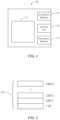
- FIG. 1illustrates a lower layer of an integrated circuit device according to an embodiment of the present invention.
- FIG. 2illustrates a plurality of layers in an integrated circuit device according to an embodiment of the present invention.
- FIG. 3illustrates a memory cell according to an embodiment of the present invention.
- FIGS. 4 A and 4 Billustrate electrical behavior of a memory cell according to an embodiment of the present invention.
- FIGS. 5 A and 5 Billustrate physical states of a memory cell according to an embodiment of the present invention.
- FIG. 6illustrates a memory array according to an embodiment of the present invention.
- FIG. 7illustrates a plurality of memory layers according to an embodiment of the present invention.
- logic level 110 of an integrated circuit devicemay include a logic sector 112 , an encryption module 114 , a decryption module 116 , and a security key 118 .
- the presence of the modules and keysmay vary according to the encryption implementation.
- Embodimentsinclude memory embedded in an integrated circuit.
- the security key 118is stored in one or more memory layers that are provided on top of the logic layer, as will be explained in more detail below.
- Embodimentsmay also include memory embedded in the logic layer itself.
Landscapes
- Engineering & Computer Science (AREA)
- Physics & Mathematics (AREA)
- Computer Hardware Design (AREA)
- Theoretical Computer Science (AREA)
- Mathematical Physics (AREA)
- Computer Security & Cryptography (AREA)
- Software Systems (AREA)
- General Engineering & Computer Science (AREA)
- General Physics & Mathematics (AREA)
- Semiconductor Memories (AREA)
Abstract
Description
This application is a continuation of U.S. patent application Ser. No. 17/354,634 filed Jun. 22, 2021, and entitled SECURE CIRCUIT INTEGRATED WITH MEMORY LAYER, which is a continuation of U.S. patent application Ser. No. 13/673,951 filed Nov. 9, 2012, and entitled SECURE CIRCUIT INTEGRATED WITH MEMORY LAYER, the disclosures of which are hereby expressly incorporated by reference herein in their respective entireties and for all purposes.
Security is a major concern for many applications of integrated circuits. Organizations invest considerable resources into the configuration of circuits, and many of these organizations wish to protect that investment. Circuits in certain applications may present inherent security concerns, such as circuits used for missile guidance systems or other sensitive military and government applications.
Due to the value of the information contained in integrated circuits, considerable efforts have been made in reverse engineering by both government and industry. Circuit transmissions can be monitored and decrypted, and the circuits themselves can be physically deconstructed by successive etching operations. Imaging operations such as scanning electron microscopy (SEM) can be conducted between successive etches to discover circuit architecture. Other imaging techniques can be used when a circuit is in operation to directly or indirectly detect heat or electricity.
Conventional methods for securing communication between integrated circuits and memory have been directed to encrypting the communications. However, this method has disadvantages. Communication circuitry is difficult to obscure, and therefore can be tapped by a dedicated reverse engineer. As technology develops, decryption techniques become more advanced, so communications that are secure today become less secure over the lifetime of a device. Some devices, such as certain aerospace applications, can have a long service life, so it is possible for current encryption techniques to become vulnerable during the lifetime of a device. In addition, if the key becomes known, access to a data stream is an undesirable vulnerability.
Embodiments of the present invention may overcome one or more problems associated with circuit security, for example by embedding a security key on one or more memory layer disposed over a logic layer in a circuit device.
In one embodiment, a secure circuit device includes a logic layer, one or more memory layers comprising non-volatile memory cells disposed over the circuit layer and integrated with the logic layer, a plurality of connectors provided between the logic layer and the one or more memory layers to electrically couple the logic layer and the one or more memory layers, and a security key disposed in the non-volatile memory cells of at least one memory layer, the security key being a key required for enabling access to the logic layer for operation.
The security circuit may include a first memory layer and a second memory layer, and non-volatile memory cells storing the security key may be one time programmable memory cells. The non-volatile memory cells may be resistive memory cells arranged in a crossbar configuration.
In an embodiment, the memory layers may include two terminal cells in a resistive memory (RRAM) a phase-change memory (PCRAM), a ferroelectric memory (FERAM), or a magnetic memory (MRAM).
A security key may include portions with a first key portion disposed in a first area, and a second key portion disposed in a second area that is vertically located with respect to the first area. In such an embodiment, the first area may be a first memory layer, and the second area may be a second memory layer disposed over the first memory layer, wherein the second security key portion is used to unlock the first security key portion, and the first security key portion is used to unlock the logic layer. An embodiment may further comprise a third security key portion disposed on a third memory layer in a third area that is vertically located with respect to the first area.
The present invention may be embodied on a system including a secure circuit device which includes a logic layer, one or more memory layers comprising non-volatile memory cells disposed over the logic layer and integrated with the logic layer in a monolithic structure, and a security key disposed in the non-volatile memory cells of at least one memory layer, the security key being a key required for enabling access to the logic layer for operation. The one or more memory layers may include a first memory layer and a second memory layer.
In an embodiment, a security circuit in the system has security key that includes a first key portion disposed in a first area, and a second key portion disposed in a second area that is vertically located with respect to the first area. The first area may be a first memory layer, and the second area may be a second memory layer disposed over the first memory layer, wherein the second security key portion is used to unlock the first security key portion, and the first security key portion is used to unlock the logic layer. The circuit in the system may further include a third security key portion disposed on a third memory layer, wherein the first, second, and third security key portions are all needed to unlock the logic layer, and a dummy key disposed in one or more memory layer.
In an embodiment of the system, the non-volatile memory cells storing the security key may be one time programmable memory cells, and in an embodiment they may include two terminal cells. The non-volatile memory cells may be resistive memory cells arranged in a crossbar configuration. The logic layer may include one or more processing or computational elements, and the system may further comprise access logic, wherein the access logic is configured to receive the security key disposed in the non-volatile memory cells and is configured to enable access to the logic layer in response thereto.
The present invention relates to a multi-layered secure device having one or more security keys distributed in one or more memory layers of the device to provide enhanced security. The memory layer is provided on top of a logic layer and form in a monolithic structure so that there would be no exposed wires (or connectors) therebetween. The wires or connectors used to couple the logic layer and the memory layer may be through silicon vias (TSV) or other suitable conductive structures (e.g., vias).
As shown inFIG.1 , in an embodiment,logic level 110 of an integrated circuit device may include alogic sector 112, anencryption module 114, adecryption module 116, and asecurity key 118. The presence of the modules and keys may vary according to the encryption implementation. Embodiments include memory embedded in an integrated circuit. In an embodiment, thesecurity key 118 is stored in one or more memory layers that are provided on top of the logic layer, as will be explained in more detail below. Embodiments may also include memory embedded in the logic layer itself.
The resistive memory device is a two-terminal device having a switching medium provided between top and bottom electrodes. The resistance of the switching medium can be controlled by applying an electrical signal to the electrodes. The electrical signal may be current-based or voltage-based, or may use a combination of current and voltage. As used herein, the term “RRAM” or “resistive memory device” or “resistive memory cell” refers to a memory device that uses a switching medium whose resistance can be controlled by applying an electrical signal without ferroelectricity, magnetization and phase change of the switching medium. Although RRAM is described in greater detail below, embodiments of the present invention may be implemented in various types of two terminal non-volatile memory, such as phase-change memory (PCRAM), ferroelectric memory (FERAM), and magnetic memory (MRAM).
In an embodiment,memory cells 300 use an amorphous-silicon-based resistive memory and use amorphous silicon (a-Si) as the switchingmedium 304. The resistance of the switching medium304 changes according to formation or retrieval of a conductive filament inside the a-Si switching medium304 according to a voltage applied. Thetop electrode 306 is a conductive layer containing silver (Ag) and acts as a source of filament-forming ions in thea-Si switching medium 304. Although silver is used in an exemplary embodiment, it will be understood that thetop electrode 306 can be formed from various other suitable metals, such as gold (Au), nickel (Ni), aluminum (Al), chromium (Cr), iron (Fe), manganese (Mn), tungsten (W), vanadium (V), and cobalt (Co). Thebottom electrode 302 is a boron-doped or other p-type polysilicon electrode that is in contact with a lower end face of thea-Si switching medium 304.
A lower portion of the switchingmedium 304 defines afilament region 504 wherein afilament 505 is formed when the program voltage Vpth is applied after the electroforming process. Theregions filament 505 includes a series of metal particles that are trapped in defect sites in the lower portion of the switchingmedium 304 when the program voltage Vpth applied provides sufficient activation energy to push a number of metal ions from themetallic region 502 toward thebottom electrode 302.
Thefilament 505 comprises a collection of metal particles that are separated from each other by the non-conducting switching medium and does not define a continuous conductive path, unlike thepath 503 in themetallic region 502. Thefilament 505 extends about 2-10 nm depending on implementation. The conduction mechanism in the ON state is electrons tunneling through the metal particles in thefilament 505. The device resistance is dominated by the tunneling resistance between ametal particle 506 and thebottom electrode 302. Themetal particle 506 is a metal particle in thefilament region 504 that is closest to thebottom electrode 302 and is the last metal particle in thefilament region 504 in the ON state.
Referring back toFIGS.4A and4B , thememory cell 300 can be controlled to exhibit a diode-like behavior by controlling the amount of current flowing through thememory cell 300. If the amount of current flowing through thememory cell 300 is less than a threshold amount, thedevice 300 exhibits a diode-like behavior, thereby preventing a reverse current flow from thebottom electrode 302 to thetop electrode 306. In an embodiment, the threshold current is 10 μA so that thememory cell 300 exhibits non-rectifying characteristics (seeFIG.4A ) if the amount of current is 10 μA or more and rectifying characteristics (seeFIG.4B ) if the amount of current is less than 10 μA. The threshold current varies according to the device implementation, e.g., the materials used and the size of thememory cell 300.
A negative potential applied to thebottom electrode 302 causes themetal particle 506 closest to the bottom electrode302 (seeFIG.5A ) to shift slightly upward without dislodging it from thefilament region 504. The resulting increased distance between themetal particle 506 and thebottom electrode 302 increases the resistance and prevents the current from flowing from thebottom electrode 302 to themetal particle 506. If the current, however, is equal to or greater than the threshold level, the large current bursts through themetal particle 506 from thebottom electrode 302.
A parallel array oftop electrodes 604 extends along a second direction to intersect thebottom electrodes 602. Thetop electrodes 604 include metals capable of supplying filament-forming ions such as silver (Ag), gold (Au), nickel (Ni), aluminum (AI), chromium (Cr), iron (Fe), manganese (Mn), tungsten (W), vanadium (V) and cobalt (Co). In an embodiment, thetop electrodes 604 and thebottom electrodes 602 are orthogonal to each other. Thetop electrodes 604 are nanowires having a width of about 60 nm and a pitch of about 120 nm.
Each intersection606 of the twoarrays electrodes bottom electrode 602. In some embodiments, each memory cell in a crossbar memory array can store a single bit. In other embodiments, the memory cells exhibit multi-level resistance thereby allowing storage of a plurality of bits at each cell. In an embodiment, the switching layer610 includes amorphous silicon or other non-crystalline silicon, but embodiments of the invention are not limited thereto.
In an embodiment, referring toFIG.2 , memory layers220 are electrically coupled tologic layer 110 and toother memory layers 220 by through silicon vias (TSVs). To enhance thermal performance, the memory cells ofmemory layers 220 may be disposed towards outer edges of the chip, so that memory cells are not directly disposed over logic components. Eachsuccessive memory layer 220 may be arranged in such a manner, so that a portion of upper memory layers does not overlap with portions of lower memory layers.
In an embodiment where memory layers220 only store keys and a relatively small amount of data or no data, memory cells storing one or more key118 may be distributed across relatively large areas of theunderlying circuit 100. A broad distribution of memory cells can help obscure the location of a key, especially when multiple keys are present.
Referring toFIG.7 , one ormore memory layer 220 may include anencryption module 114, adecryption module 116, and asecurity key 118. Alternatively, eachmemory layer 220 may include asecurity key 118, but not anencryption module 114 ordecryption module 116.
The one ormore security key 118 in amemory layer 220 may be set at any phase of its lifecycle. The key could be set during the fabrication process, for example by setting memory states at or immediately following fabrication. In some applications, it may be desirable for the security key to be set by a customer further down the supply chain, such as an original equipment manufacturer, a reseller, or even an end user.
Thesecurity key 118 can be set by using a one-time programmable (OTP) process. An example of OTP process is an anti-fuse process, which is well known. In an embodiment, amemory layer 220 includes a large number of potential antifuse locations, so that it is difficult to determine which anti-fuses have been activated in a particular application through imaging techniques.
In an embodiment, a plurality ofsecurity keys 118 that are distributed on different memory layers220-1 to220-nmay include “dummy” keys that are not used by thedevice 100, but are provided to make it more difficult to determine which security key is used by thedevice 100.
In an embodiment, data are in the memory layers220 are encrypted using keys as shown inFIG.8C . Symmetrical keys are used to encrypt the data transmission, where one or more key118 disposed onlogic layer 110 corresponds to one or more key118 disposed on memory layers220. Alternatively, thekeys 118 may all be stored in the memory layers220.
Thekeys 118 could be distributed among the memory layers220 in a convoluted fashion to further obscure key values and locations. For example, the key118 used bylogic layer 110 to decrypt data from memory layer220-1 may be stored on memory layer220-2, or portions of each key may be distributed among several memory layers as discussed above with respect toFIG.8B . Having a plurality of keys present in various forms and layers enhances the difficulty of reverse engineering acircuit 100.
Any number of encryption schemes may be used by embodiments of the present invention. For example, thedevice 100 may use the data encryption standard (DES) or the advanced encryption standard (AES) with one ormore keys 118 of an arbitrary length. Embodiments can implement symmetric key or asymmetric keys as appropriate. Embodiments of the present invention are not limited to any particular length or encryption scheme.
Different encryption schemes can be used in thesame device 100 for different purposes. For example, external communications may use AES, while internal storage may be encrypted with DES.
In an embodiment, thedevice 100 includes a field programmable gate array (FPGA) so that the logic can be configured after the circuit is fabricated. The logic configuration of an FPGA is stored (programmed) in a memory, and is loaded into the logic when power is applied to the circuit. This communication may involve a bit stream up to millions of bits, depending on the complexity of the logic. In a secure implementation, these bits are encrypted.
In addition to providing secure intra-chip communications, an embodiment that uses an FPGA as alower layer 110 can storekeys 118 for communication with external devices. Embodiments described above with respect toFIGS.1-8 can be implemented using an FPGA as alogic layer 110.
The present invention is not restricted to a particular configuration of thelogic layer 110. As circuit technology progresses, the line between an ASIC, an FPGA, and other similar set or programmable circuits blurs as hybrid devices enter the market. Any of these circuits can implement security through one ormore memory layers 220 as described herein.
A system employing acircuit device 100 as described above may be implemented in many different configurations. In one embodiment, as shown inFIG.9 , thedevice 100 is implemented in acomputer system 900. AlthoughFIG.9 showsdevice 100 as being discrete from computer subsystems, it can be implemented as a component of any of the subsystems or other components, such asstorage subsystem 912,network interface 906, or userinterface output devices 908.
Userinterface input devices 910 may include a keyboard, pointing devices such as a mouse, trackball, touchpad, or graphics tablet, a scanner, a barcode scanner for scanning article barcodes, a touchscreen incorporated into the display, audio input devices such as voice recognition systems, microphones, and other types of input devices. In general, use of the term “input device” is intended to include all possible types of devices and ways to input information intocomputer system 900 or ontocommunication network 922.
Userinterface output devices 908 may include a display subsystem, a printer, a fax machine, or non-visual displays such as audio output devices. The display subsystem may be a cathode ray tube (CRT), a flat-panel device such as a liquid crystal display (LCD), or a projection device. The display subsystem may also provide non-visual display such as via audio output devices. In general, use of the term “output device” is intended to include all possible types of devices and ways to output information fromcomputer system 900 to a user or to another machine or computer system.
Another example of a system which may incorporatedevice 100 is a packageddevice 1000, as shown inFIG.10 . Packageddevice 1000 may include one ormore processors 1002,memory 1004, I/O port 1006, and electrical components such as aresistor 1008 and a capacitor1010. The I/O port 1006 may be a typical interface such as a universal serial bus (USB), a proprietary interface, or the like. In some embodiments, the interface may use light or radio waves to transmit data into and out of the system in apackage 1000. A system in apackage 1000 may be incorporated along with other components into a device such as acomputer system 900 or another electronic device.
Yet another example of a system which may incorporatedevice 100 is a system on achip 1100, as shown inFIG.11 . A system on a chip may comprise one ormore processor 1102,memory 1104, I/O interface 1106, andpower management module 1108, all integrated into a single chip. Persons of skill in the art will recognize that various embodiments of a system on achip 1100 may have more or less components than those shown inFIG.11 . Various components may be disposed on the same layer, or stacked above one another on separate layers.
Embodiments according to the present disclosure have advantages over conventional devices. For example, certain security functions may be made redundant by a multi-layeredsecure device 100. An exemplary function that may be made redundant is a checksum operation that is conducted for security purposes, particularly in telecom applications. Although a checksum operation may still be performed to ensure data accuracy, in an embodiment, it may not be necessary to perform a checksum to determine whether a device has been compromised. Eliminating such functions may reduce the cost and complexity of devices according to the above disclosure, as well as reducing boot and transmission times.
An exemplary embodiment comprising a plurality ofmemory layers 220, each comprising asecurity key 118 or security key portion118-n, makes it considerably more difficult to reverse engineer acircuit 100. To accurately image thelower logic level 110, a reverse engineer etches upper memory layers118-1 to118-n, thereby destroyingsecurity keys 118 and any additional data stored in memory. With the security keys destroyed, the device will not function, making it more difficult to image operations of thelogic layer 110.
Persons of skill in the art will recognize these and other advantages. Although the invention has been described using structures of exemplary embodiments, embodiments of the invention are not necessarily limited thereto. The above description is intended to be illustrative, and not limiting.
Claims (20)
1. A secure semiconductor chip, comprising:
a logic layer and a logic circuit formed within the logic layer;
access logic configured to provide access to or deny access to the logic circuit formed within the logic layer;
a first memory layer comprising non-volatile resistive memory cells and integrated with the logic layer in a monolithic structure embodying the secure semiconductor chip; and
a plurality of connectors within vias provided between the logic layer and the first memory layer facilitating intra-chip communication within an interior of the secure semiconductor chip; wherein:
the access logic is configured to retrieve security data stored in the non-volatile resistive memory cells of the first memory layer by way of the plurality of connectors, and
the access logic is configured to provide access to the logic circuit formed within the logic layer in response at least in part to successful retrieval of the security data.
2. The secure semiconductor chip ofclaim 1 , wherein the security data comprises:
a first portion of the security data disposed in a first group of the non-volatile resistive memory cells; and
a second portion of the security data disposed in a second group of the non-volatile resistive memory cells.
3. The secure semiconductor chip ofclaim 2 , wherein the access logic:
retrieves the first portion of the security data from the first group of the non-volatile resistive memory cells,
retrieves the second portion of the security data from the second group of the non-volatile resistive memory cells, and
combines the first portion of the security data with the second portion of the security data to form a security key that facilitates the providing access to the logic circuit.
4. The secure semiconductor chip ofclaim 2 , wherein the access logic utilizes:
the first portion of the security data to access the logic circuit and unlock access to the second portion of the security data.
5. The secure semiconductor chip ofclaim 1 , wherein the plurality of connectors within vias are not exposed to an exterior of the monolithic structure.
6. The secure semiconductor chip ofclaim 1 , wherein the first memory layer is vertically located within the monolithic structure with respect to the logic layer.
7. The secure semiconductor chip ofclaim 1 , further comprising an interface, wherein the security data is stored in the non-volatile resistive memory cells of the first memory layer post-fabrication in response to an input received at the interface.
8. The secure semiconductor chip ofclaim 1 , wherein the first memory layer stores dummy security data that is not utilized by the access logic for providing access to the logic circuit.
9. The secure semiconductor chip ofclaim 1 , further comprising volatile memory formed in the logic layer and communicatively connected to the access logic or to the logic circuit.
10. The secure semiconductor chip ofclaim 1 , further comprising a second security data stored on the logic layer, wherein the security data and the second security data facilitate encryption of data to form encrypted data and decryption of the encrypted data, wherein the encrypted data is in memory on the logic layer or is stored in the first memory layer or in a second memory layer of the monolithic structure of the secure semiconductor chip.
11. The secure semiconductor chip ofclaim 1 wherein the logic circuit comprises a programmable circuit configurable after fabrication of the secure semiconductor chip with a logic configuration.
12. The secure semiconductor chip ofclaim 11 , wherein the logic configuration includes second security data stored at the secure semiconductor chip and is retrieved by the access logic in response to the successful retrieval of the security data, wherein the logic configuration and the second security data are usable in conjunction with executing the logic circuit.
13. A system embodied on a secure semiconductor chip, comprising:
a monolithic structure comprising a plurality of layers, the plurality of layers including:
a logic layer comprising an access logic and a logic circuit;
a memory layer comprising non-volatile memory;
a connector between the logic layer and the memory layer that electrically couples the logic layer and the memory layer providing secure intra-chip communication there between; and
a security key stored in the non-volatile memory of the memory layer, wherein the access logic is configured to retrieve the security key from the non-volatile memory utilizing the connector and the intra-chip communication in conjunction with permitting access to the logic circuit of the logic layer.
14. The system ofclaim 13 , further comprising an interface facilitating communication between the system and an external device.
15. The system ofclaim 14 , wherein the logic circuit comprises a programmable circuit configurable after fabrication of the secure semiconductor chip and at least in part by way of the interface.
16. The system ofclaim 15 , wherein a logic configuration of the programmable circuit is stored in the memory layer and includes additional security data.
17. The system ofclaim 16 , wherein the logic configuration and additional security data of the programmable circuit are loaded into the programmable circuit from the memory layer by way of the connector and the intra-chip communication there between.
18. The system ofclaim 14 , wherein the logic configuration and the additional security data are usable in conjunction with executing the logic circuit.
19. The system ofclaim 13 , wherein access to the logic circuit of the logic layer facilitates access to second security data stored in the secure semiconductor chip.
20. The system ofclaim 19 , wherein retrieval of the second security data is usable in conjunction with execution of at least one of:
a programmable logic circuit of the logic layer;
a set logic circuit at the logic layer; or
a hybrid fixed and programmable logic circuit at the logic layer.
Priority Applications (1)
| Application Number | Priority Date | Filing Date | Title |
|---|---|---|---|
| US18/529,596US12254124B1 (en) | 2012-11-09 | 2023-12-05 | Secure circuit integrated with memory layer |
Applications Claiming Priority (3)
| Application Number | Priority Date | Filing Date | Title |
|---|---|---|---|
| US13/673,951US11068620B2 (en) | 2012-11-09 | 2012-11-09 | Secure circuit integrated with memory layer |
| US17/354,634US11836277B2 (en) | 2012-11-09 | 2021-06-22 | Secure circuit integrated with memory layer |
| US18/529,596US12254124B1 (en) | 2012-11-09 | 2023-12-05 | Secure circuit integrated with memory layer |
Related Parent Applications (1)
| Application Number | Title | Priority Date | Filing Date |
|---|---|---|---|
| US17/354,634ContinuationUS11836277B2 (en) | 2012-11-09 | 2021-06-22 | Secure circuit integrated with memory layer |
Publications (1)
| Publication Number | Publication Date |
|---|---|
| US12254124B1true US12254124B1 (en) | 2025-03-18 |
Family
ID=50682903
Family Applications (3)
| Application Number | Title | Priority Date | Filing Date |
|---|---|---|---|
| US13/673,951Active2035-03-25US11068620B2 (en) | 2012-11-09 | 2012-11-09 | Secure circuit integrated with memory layer |
| US17/354,634Active2032-11-27US11836277B2 (en) | 2012-11-09 | 2021-06-22 | Secure circuit integrated with memory layer |
| US18/529,596ActiveUS12254124B1 (en) | 2012-11-09 | 2023-12-05 | Secure circuit integrated with memory layer |
Family Applications Before (2)
| Application Number | Title | Priority Date | Filing Date |
|---|---|---|---|
| US13/673,951Active2035-03-25US11068620B2 (en) | 2012-11-09 | 2012-11-09 | Secure circuit integrated with memory layer |
| US17/354,634Active2032-11-27US11836277B2 (en) | 2012-11-09 | 2021-06-22 | Secure circuit integrated with memory layer |
Country Status (3)
| Country | Link |
|---|---|
| US (3) | US11068620B2 (en) |
| CN (1) | CN103811069A (en) |
| TW (1) | TW201435643A (en) |
Families Citing this family (4)
| Publication number | Priority date | Publication date | Assignee | Title |
|---|---|---|---|---|
| US10296738B2 (en)* | 2017-05-03 | 2019-05-21 | Nuvoton Technology Corporation | Secure integrated-circuit state management |
| FR3069677A1 (en) | 2017-07-27 | 2019-02-01 | Stmicroelectronics (Crolles 2) Sas | DEVICE FOR GENERATING A RANDOM NUMBER |
| US11437102B1 (en)* | 2021-03-05 | 2022-09-06 | International Business Machines Corporation | Memory erasure using proximity heaters |
| EP4510023A1 (en)* | 2023-08-17 | 2025-02-19 | Nagravision Sàrl | Data processing component and computer processor |
Citations (234)
| Publication number | Priority date | Publication date | Assignee | Title |
|---|---|---|---|---|
| US680652A (en) | 1897-11-08 | 1901-08-13 | Leonard L Elden | Circuit-breaker. |
| US4433468A (en) | 1980-03-26 | 1984-02-28 | Nippon Electric Co., Ltd. | Method for making semiconductor device having improved thermal stress characteristics |
| US4684972A (en) | 1981-08-07 | 1987-08-04 | The British Petroleum Company, P.L.C. | Non-volatile amorphous semiconductor memory device utilizing a forming voltage |
| US4741601A (en) | 1984-10-08 | 1988-05-03 | Nec Corporation | Non-linear device for driving liquid crystal display |
| US5139911A (en) | 1989-01-04 | 1992-08-18 | Fuji Xerox Co., Ltd. | Electrophotographic photoreceptor with two part surface layer |
| US5242855A (en) | 1991-09-30 | 1993-09-07 | Nec Corporation | Method of fabricating a polycrystalline silicon film having a reduced resistivity |
| US5278085A (en) | 1992-08-11 | 1994-01-11 | Micron Semiconductor, Inc. | Single mask process for forming both n-type and p-type gates in a polycrystalline silicon layer during the formation of a semiconductor device |
| US5315131A (en) | 1990-11-22 | 1994-05-24 | Matsushita Electric Industrial Co., Ltd. | Electrically reprogrammable nonvolatile memory device |
| US5335219A (en) | 1991-01-18 | 1994-08-02 | Ovshinsky Stanford R | Homogeneous composition of microcrystalline semiconductor material, semiconductor devices and directly overwritable memory elements fabricated therefrom, and arrays fabricated from the memory elements |
| US5360981A (en) | 1989-05-11 | 1994-11-01 | British Telecommunications Public Limited Company | Amorphous silicon memory |
| US5457649A (en) | 1994-08-26 | 1995-10-10 | Microchip Technology, Inc. | Semiconductor memory device and write-once, read-only semiconductor memory array using amorphous-silicon and method therefor |
| US5538564A (en) | 1994-03-18 | 1996-07-23 | Regents Of The University Of California | Three dimensional amorphous silicon/microcrystalline silicon solar cells |
| US5541869A (en) | 1991-10-22 | 1996-07-30 | British Telecommunications, Plc | Resistive memory element |
| US5594363A (en) | 1995-04-07 | 1997-01-14 | Zycad Corporation | Logic cell and routing architecture in a field programmable gate array |
| US5614756A (en) | 1990-04-12 | 1997-03-25 | Actel Corporation | Metal-to-metal antifuse with conductive |
| US5645628A (en) | 1994-07-14 | 1997-07-08 | Matsushita Electric Industrial Co., Ltd. | Electroless plating bath used for forming a wiring of a semiconductor device, and method of forming a wiring of a semiconductor device |
| US5751012A (en) | 1995-06-07 | 1998-05-12 | Micron Technology, Inc. | Polysilicon pillar diode for use in a non-volatile memory cell |
| US5840608A (en) | 1996-11-22 | 1998-11-24 | United Microelectronics Corporation | High density ROM and a method of making the same |
| US5970332A (en) | 1995-03-28 | 1999-10-19 | U.S. Philips Corporation | Method of manufacturing a semiconductor device with a BiCMOS circuit |
| US5998244A (en) | 1996-08-22 | 1999-12-07 | Micron Technology, Inc. | Memory cell incorporating a chalcogenide element and method of making same |
| US6128214A (en) | 1999-03-29 | 2000-10-03 | Hewlett-Packard | Molecular wire crossbar memory |
| US6143642A (en) | 1997-12-22 | 2000-11-07 | Vlsi Technology, Inc. | Programmable semiconductor structures and methods for making the same |
| US6259116B1 (en) | 1997-10-22 | 2001-07-10 | U.S. Philips Corporation | Multiple memory element semiconductor memory devices |
| US6291836B1 (en) | 1996-06-05 | 2001-09-18 | U. S. Philips Corporation | Method of operating a programmable, non-volatile memory device |
| US6436818B1 (en) | 1997-02-19 | 2002-08-20 | Micron Technology, Inc. | Semiconductor structure having a doped conductive layer |
| US6436765B1 (en) | 2001-02-09 | 2002-08-20 | United Microelectronics Corp. | Method of fabricating a trenched flash memory cell |
| US6492694B2 (en) | 1998-02-27 | 2002-12-10 | Micron Technology, Inc. | Highly conductive composite polysilicon gate for CMOS integrated circuits |
| US20030036238A1 (en) | 2000-12-22 | 2003-02-20 | The Regents Of The University Of California | Process for direct integration of a thin-film silicon p-n junction diode with a magnetic tunnel junction |
| WO2003034498A1 (en) | 2001-10-16 | 2003-04-24 | Midwest Research Institute | Stacked switchable element and diode combination |
| US20030141565A1 (en) | 2002-01-28 | 2003-07-31 | Fumihiko Hirose | Diode |
| US6627530B2 (en) | 2000-12-22 | 2003-09-30 | Matrix Semiconductor, Inc. | Patterning three dimensional structures |
| US20040026682A1 (en) | 2002-06-17 | 2004-02-12 | Hai Jiang | Nano-dot memory and fabricating same |
| US20040059908A1 (en)* | 2001-10-29 | 2004-03-25 | Keiki Yamada | Encrypted communication apparatus |
| US6762474B1 (en) | 1998-06-10 | 2004-07-13 | Agere Systems Inc. | Method and apparatus for temperature compensation of read-only memory |
| US6768157B2 (en) | 2001-08-13 | 2004-07-27 | Advanced Micro Devices, Inc. | Memory device |
| US20040170040A1 (en) | 2002-08-02 | 2004-09-02 | Unity Semiconductor Corporation | Rewritable memory with non-linear memory element |
| US6815286B2 (en) | 2001-08-13 | 2004-11-09 | Advanced Micro Devices, Inc. | Memory device |
| US6838720B2 (en) | 2001-08-13 | 2005-01-04 | Advanced Micro Devices, Inc. | Memory device with active passive layers |
| US20050020510A1 (en) | 2002-08-29 | 2005-01-27 | Benedict Dale L. | D-mannose contraceptives |
| US20050029587A1 (en) | 1995-06-07 | 2005-02-10 | Harshfield Steven T. | Method and apparatus for forming an integrated circuit electrode having a reduced contact area |
| US6858482B2 (en) | 2002-04-10 | 2005-02-22 | Micron Technology, Inc. | Method of manufacture of programmable switching circuits and memory cells employing a glass layer |
| US6858481B2 (en) | 2001-08-13 | 2005-02-22 | Advanced Micro Devices, Inc. | Memory device with active and passive layers |
| US6864127B2 (en) | 1997-04-25 | 2005-03-08 | Semiconductor Energy Laboratory Co., Ltd. | Semiconductor device and method of fabricating the same |
| US20050052915A1 (en) | 2002-12-19 | 2005-03-10 | Matrix Semiconductor, Inc. | Nonvolatile memory cell without a dielectric antifuse having high- and low-impedance states |
| US20050062045A1 (en) | 2002-10-02 | 2005-03-24 | Arup Bhattacharyya | Processes of forming stacked resistor constructions |
| US20050073881A1 (en) | 2003-10-06 | 2005-04-07 | Tran Lung The | Magnetic memory device including groups of series-connected memory elements |
| US6881994B2 (en) | 2000-08-14 | 2005-04-19 | Matrix Semiconductor, Inc. | Monolithic three dimensional array of charge storage devices containing a planarized surface |
| US6927430B2 (en) | 2001-06-28 | 2005-08-09 | Sharp Laboratories Of America, Inc. | Shared bit line cross-point memory array incorporating P/N junctions |
| US6939787B2 (en) | 1999-12-28 | 2005-09-06 | Fujitsu Limited | Method for fabricating semiconductor device having gate electrode with polymetal structure of polycrystalline silicon film and metal film |
| US6946719B2 (en) | 2003-12-03 | 2005-09-20 | Matrix Semiconductor, Inc | Semiconductor device including junction diode contacting contact-antifuse unit comprising silicide |
| US20060017488A1 (en) | 2004-07-21 | 2006-01-26 | Sharp Laboratories Of America, Inc. | Mono-polarity switchable PCMO resistor trimmer |
| TWI250424B (en) | 2002-01-08 | 2006-03-01 | Intel Corp | Method and apparatus for enhancing multiway radix tree |
| US7020006B2 (en) | 2002-08-02 | 2006-03-28 | Unity Semiconductor Corporation | Discharge of conductive array lines in fast memory |
| US7023093B2 (en) | 2002-10-24 | 2006-04-04 | International Business Machines Corporation | Very low effective dielectric constant interconnect Structures and methods for fabricating the same |
| US20060095771A1 (en)* | 2004-11-02 | 2006-05-04 | Guido Appenzeller | Security device for cryptographic communications |
| US7073069B1 (en)* | 1999-05-07 | 2006-07-04 | Infineon Technologies Ag | Apparatus and method for a programmable security processor |
| US7102150B2 (en) | 2001-05-11 | 2006-09-05 | Harshfield Steven T | PCRAM memory cell and method of making same |
| US7122853B1 (en) | 2004-08-17 | 2006-10-17 | Fasl, Inc. | Method to improve yield and simplify operation of polymer memory cells |
| US20060281244A1 (en) | 2005-06-08 | 2006-12-14 | Masayuki Ichige | Nonvolatile semiconductor memory device and method of manufacturing the same |
| US20060289658A1 (en)* | 2003-09-04 | 2006-12-28 | Infineon Technologies Ag | Processor circuit and method of allocating a logic chip to a memory chip |
| US20070008773A1 (en) | 2005-07-11 | 2007-01-11 | Matrix Semiconductor, Inc. | Nonvolatile memory cell comprising switchable resistor and transistor |
| US20070015348A1 (en) | 2005-07-18 | 2007-01-18 | Sharp Laboratories Of America, Inc. | Crosspoint resistor memory device with back-to-back Schottky diodes |
| US7167387B2 (en) | 2003-10-23 | 2007-01-23 | Matsushita Electric Industrial Co., Ltd. | Variable resistance element, method of manufacturing the element, memory containing the element, and method of driving the memory |
| US20070045615A1 (en) | 2005-08-31 | 2007-03-01 | Samsung Electronics Co., Ltd. | Non-volatile organic resistance random access memory device and method of manufacturing the same |
| US7187577B1 (en) | 2005-11-23 | 2007-03-06 | Grandis, Inc. | Method and system for providing current balanced writing for memory cells and magnetic devices |
| US20070087508A1 (en) | 2003-12-03 | 2007-04-19 | Herner S B | Method for making a p-i-n diode crystallized adjacent to a silicide in series with a dielectric antifuse |
| US20070090425A1 (en) | 2005-09-28 | 2007-04-26 | Matrix Semiconductor, Inc. | Memory cell comprising switchable semiconductor memory element with trimmable resistance |
| US20070105390A1 (en) | 2005-11-09 | 2007-05-10 | Oh Travis B | Oxygen depleted etching process |
| US20070105284A1 (en) | 2003-12-03 | 2007-05-10 | Herner S B | Method for forming a memory cell comprising a semiconductor junction diode crystallized adjacent to a silicide |
| US7221599B1 (en) | 2004-11-01 | 2007-05-22 | Spansion, Llc | Polymer memory cell operation |
| US7238607B2 (en) | 2002-12-19 | 2007-07-03 | Sandisk 3D Llc | Method to minimize formation of recess at surface planarized by chemical mechanical planarization |
| US20070205510A1 (en) | 2006-03-03 | 2007-09-06 | Lavoie Adrien R | Noble metal barrier layers |
| US7274587B2 (en) | 2004-11-10 | 2007-09-25 | Kabushiki Kaisha Toshiba | Semiconductor memory element and semiconductor memory device |
| US20070228414A1 (en) | 2006-03-31 | 2007-10-04 | Sandisk 3D, Llc | Heterojunction device comprising a semiconductor and a resistivity-switching oxide or nitride |
| JP2007281208A (en) | 2006-04-07 | 2007-10-25 | Matsushita Electric Ind Co Ltd | Multilayer variable resistance element array, variable resistance device, multilayer nonvolatile memory element array, and nonvolatile memory device |
| US7289353B2 (en) | 2004-08-17 | 2007-10-30 | Spansion, Llc | Systems and methods for adjusting programming thresholds of polymer memory cells |
| US20070284575A1 (en) | 2005-07-18 | 2007-12-13 | Sharp Laboratories Of America, Inc. | Metal/semiconductor/metal current limiter |
| US20070290186A1 (en) | 2006-05-04 | 2007-12-20 | El Mostafa Bourim | Non-volatile variable resistance memory device and method of fabricating the same |
| JP2007328857A (en) | 2006-06-07 | 2007-12-20 | Sony Corp | Storage device |
| US20070295950A1 (en) | 2006-06-27 | 2007-12-27 | Samsung Electronics Co., Ltd. | Variable resistance random access memory device and a method of fabricating the same |
| US20080002481A1 (en) | 2002-12-20 | 2008-01-03 | Dietmar Gogl | Integrated Circuit, Method of Operating an Integrated Circuit, Method of Manufacturing an Integrated Circuit, Memory Module, Stackable Memory Module |
| US20080006907A1 (en) | 2006-07-06 | 2008-01-10 | Samsung Electronics Co., Ltd | Non-volatile memory device including a variable resistance material |
| US7324363B2 (en) | 2005-12-12 | 2008-01-29 | Synopsys, Inc. | SPICE optimized for arrays |
| US20080048164A1 (en) | 2006-07-11 | 2008-02-28 | Matsushita Electric Industrial Co., Ltd. | Electro-resistance element, method of manufacturing the same and electro-resistance memory using the same |
| US20080089110A1 (en) | 2006-10-16 | 2008-04-17 | Warren Robinett | Crossbar-memory systems and methods for writing to and reading from crossbar memory junctions of crossbar-memory systems |
| US20080090337A1 (en) | 2006-10-03 | 2008-04-17 | Williams R Stanley | Electrically actuated switch |
| US7365411B2 (en) | 2004-08-12 | 2008-04-29 | Micron Technology, Inc. | Resistance variable memory with temperature tolerant materials |
| US20080106925A1 (en) | 2006-11-08 | 2008-05-08 | Symetrix Corporation | Correlated electron memory |
| US20080106926A1 (en) | 2006-11-08 | 2008-05-08 | Symetrix Corporation | Non-volatile resistance switching memories and methods of making same |
| CN101208705A (en) | 2005-06-24 | 2008-06-25 | 伊姆西公司 | Storage data encryption |
| US7402847B2 (en) | 2005-04-13 | 2008-07-22 | Axon Technologies Corporation | Programmable logic circuit and method of using same |
| US7405418B2 (en) | 2004-02-17 | 2008-07-29 | Infineon Technologies Ag | Memory device electrode with a surface structure |
| US20080185567A1 (en) | 2007-02-05 | 2008-08-07 | Nitin Kumar | Methods for forming resistive switching memory elements |
| US20080206931A1 (en) | 2002-07-26 | 2008-08-28 | Laurent Breuil | Nonvolatile memory element and production method thereof and storage memory arrangement |
| US20080205179A1 (en) | 2007-02-28 | 2008-08-28 | Qimonda Ag | Integrated circuit having a memory array |
| US20080220601A1 (en) | 2007-03-05 | 2008-09-11 | Nitin Kumar | Methods for forming nonvolatile memory elements with resistive-switching metal oxides |
| US20080232160A1 (en) | 2007-02-27 | 2008-09-25 | International Business Machines Corporation | Rectifying element for a crosspoint based memory array architecture |
| US20080278990A1 (en) | 2007-05-09 | 2008-11-13 | Pragati Kumar | Resistive-switching nonvolatile memory elements |
| US20080304312A1 (en) | 2007-06-11 | 2008-12-11 | Macronix International Co., Ltd. | Resistance memory with tungsten compound and manufacturing |
| US20080311722A1 (en) | 2007-06-15 | 2008-12-18 | Sandisk 3D Llc | Method for forming polycrystalline thin film bipolar transistors |
| US20090001345A1 (en) | 2007-06-29 | 2009-01-01 | April Schricker | Memory cell that employs a selectively deposited reversible resistance-switching element and methods of forming the same |
| US7474000B2 (en) | 2003-12-05 | 2009-01-06 | Sandisk 3D Llc | High density contact to relaxed geometry layers |
| WO2009005699A1 (en) | 2007-06-29 | 2009-01-08 | Sandisk 3D, Llc | Memory cell that employs a selectively grown reversible resistance-switching element and methods of forming the same |
| US20090014707A1 (en) | 2006-10-20 | 2009-01-15 | Wei Lu | Non-volatile solid state resistive switching devices |
| US20090052226A1 (en) | 2007-08-24 | 2009-02-26 | Samsung Electronics Co., Ltd | Resistive random access memory device |
| US7499355B2 (en) | 2006-07-31 | 2009-03-03 | Sandisk 3D Llc | High bandwidth one time field-programmable memory |
| US20090065591A1 (en)* | 2007-09-12 | 2009-03-12 | Seiko Epson Corporation | Smart-card chip arrangement |
| US7511532B2 (en) | 2005-11-03 | 2009-03-31 | Cswitch Corp. | Reconfigurable logic structures |
| US20090095951A1 (en) | 2007-10-12 | 2009-04-16 | Ovonyx, Inc. | Memory Device With Low Reset Current |
| US7521705B2 (en) | 2005-08-15 | 2009-04-21 | Micron Technology, Inc. | Reproducible resistance variable insulating memory devices having a shaped bottom electrode |
| US7534625B2 (en) | 2004-09-24 | 2009-05-19 | Karpov Ilya V | Phase change memory with damascene memory element |
| US7541252B2 (en) | 2006-11-09 | 2009-06-02 | Samsung Electronics Co., Ltd. | Methods of fabricating a semiconductor device including a self-aligned cell diode |
| US20090152737A1 (en) | 2000-07-14 | 2009-06-18 | Micron Technology, Inc. | Memory devices having contact features |
| US7550380B2 (en) | 2004-11-03 | 2009-06-23 | Micron Technology, Inc. | Electroless plating of metal caps for chalcogenide-based memory devices |
| US20090168486A1 (en) | 2007-12-27 | 2009-07-02 | Sandisk 3D Llc | Large capacity one-time programmable memory cell using metal oxides |
| US20090182965A1 (en)* | 2008-01-10 | 2009-07-16 | Unity Semiconductor Corporation | Securing data in memory device |
| US7566643B2 (en) | 2007-07-23 | 2009-07-28 | Ovonyx, Inc. | Liquid phase deposition of contacts in programmable resistance and switching devices |
| US20090231910A1 (en) | 2008-03-11 | 2009-09-17 | Micron Technology, Inc. | Non-volatile memory with resistive access component |
| US20090250787A1 (en) | 2008-04-07 | 2009-10-08 | Toshie Kutsunai | Semiconductor storage device and manufacturing method of the same |
| US20090257265A1 (en) | 2008-04-11 | 2009-10-15 | Sandisk 3D Llc | Multilevel nonvolatile memory device containing a carbon storage material and methods of making and using same |
| US20090256130A1 (en) | 2008-04-11 | 2009-10-15 | Sandisk 3D Llc | Memory cell that employs a selectively fabricated carbon nano-tube reversible resistance-switching element, and methods of forming the same |
| US7606059B2 (en) | 2003-03-18 | 2009-10-20 | Kabushiki Kaisha Toshiba | Three-dimensional programmable resistance memory device with a read/write circuit stacked under a memory cell array |
| US20090267047A1 (en) | 2008-04-28 | 2009-10-29 | Hitachi, Ltd. | Semiconductor memory device and manufacturing method thereof |
| US7615439B1 (en) | 2008-09-29 | 2009-11-10 | Sandisk Corporation | Damascene process for carbon memory element with MIIM diode |
| US20090298224A1 (en) | 2002-12-13 | 2009-12-03 | Lowrey Tyler A | Memory and Access Device and Method Therefor |
| US20090321789A1 (en) | 2008-06-30 | 2009-12-31 | Sandisk 3D Llc | Triangle two dimensional complementary patterning of pillars |
| US20100007937A1 (en) | 2006-11-09 | 2010-01-14 | Sage Electrochromics, Inc. | Method of making an ion-switching device without a separate lithiation step |
| US20100012914A1 (en) | 2008-07-18 | 2010-01-21 | Sandisk 3D Llc | Carbon-based resistivity-switching materials and methods of forming the same |
| US20100019221A1 (en) | 2008-07-22 | 2010-01-28 | Macronix International Co., Ltd. | Fully self-aligned pore-type memory cell having diode access device |
| US20100019310A1 (en) | 2008-07-25 | 2010-01-28 | Kabushiki Kaisha Toshiba | Semiconductor memory device |
| US20100032638A1 (en) | 2008-08-07 | 2010-02-11 | Sandisk 3D Llc | Memory cell that includes a carbon-based memory element and methods of forming the same |
| US20100039136A1 (en) | 2008-08-15 | 2010-02-18 | Qualcomm Incorporated | Gate Level Reconfigurable Magnetic Logic |
| US20100044708A1 (en) | 2008-08-19 | 2010-02-25 | Chunghwa Picture Tubes, Ltd. | Thin film transistor, pixel structure and fabrication methods thereof |
| US20100085798A1 (en) | 2008-10-08 | 2010-04-08 | The Regents Of The University Of Michigan | Silicon-based nanoscale resistive device with adjustable resistance |
| US20100084625A1 (en) | 2008-10-02 | 2010-04-08 | Guy Wicker | Memory Device |
| US20100090192A1 (en) | 2006-08-31 | 2010-04-15 | Nxp, B.V. | Method for controlled formation of the resistive switching material in a resistive switching device and device obtained thereof |
| US20100102290A1 (en) | 2008-10-20 | 2010-04-29 | The Regents Of The University Of Michigan | Silicon based nanoscale crossbar memory |
| US20100101290A1 (en) | 2008-10-24 | 2010-04-29 | Antonio Bertolotto | Method for the production of an agent for treatment of agricultural soils |
| US7719001B2 (en) | 2006-06-28 | 2010-05-18 | Semiconductor Energy Laboratory Co., Ltd | Semiconductor device with metal oxides and an organic compound |
| US7729158B2 (en) | 2003-04-03 | 2010-06-01 | Kabushiki Kaisha Toshiba | Resistance change memory device |
| US7728318B2 (en) | 2006-11-16 | 2010-06-01 | Sandisk Corporation | Nonvolatile phase change memory cell having a reduced contact area |
| CN101740111A (en) | 2008-11-11 | 2010-06-16 | 国民技术股份有限公司 | Semiconductor memory device and method thereof for realizing safe memory of data |
| US20100157710A1 (en) | 2008-12-19 | 2010-06-24 | Unity Semiconductor Corporation | Array Operation Using A Schottky Diode As a Non-Ohmic Isolation Device |
| US20100157651A1 (en) | 2008-12-18 | 2010-06-24 | Sandisk 3D Llc | Method of programming a nonvolatile memory device containing a carbon storage material |
| US20100159688A1 (en)* | 2008-12-19 | 2010-06-24 | Unity Semiconductor Corporation | Device fabrication |
| US20100163828A1 (en) | 2008-12-30 | 2010-07-01 | Industrial Technology Research Institute | Phase change memory devices and methods for fabricating the same |
| US7749805B2 (en) | 2005-03-10 | 2010-07-06 | Qimonda Ag | Method for manufacturing an integrated circuit including an electrolyte material layer |
| US20100176368A1 (en) | 2009-01-14 | 2010-07-15 | Ko Nikka | Method of manufacturing semiconductor memory device, and semiconductor memory device |
| US7760538B1 (en) | 2008-03-04 | 2010-07-20 | Xilinx, Inc. | Non-volatile SRAM cell |
| US7772581B2 (en) | 2006-09-11 | 2010-08-10 | Macronix International Co., Ltd. | Memory device having wide area phase change element and small electrode contact area |
| US7786464B2 (en) | 2007-11-20 | 2010-08-31 | Infineon Technologies Ag | Integrated circuit having dielectric layer including nanocrystals |
| US7786589B2 (en) | 2006-12-06 | 2010-08-31 | Kabushiki Kaisha Toshiba | Semiconductor device and method for manufacturing semiconductor device |
| US20100221868A1 (en) | 2007-12-04 | 2010-09-02 | Regino Sandoval | Active Material Devices with Containment Layer |
| US20100219510A1 (en) | 2008-06-30 | 2010-09-02 | Sandisk 3D Llc | Method for fabricating high density pillar structures by double patterning using positive photoresist |
| US7824956B2 (en) | 2007-06-29 | 2010-11-02 | Sandisk 3D Llc | Memory cell that employs a selectively grown reversible resistance-switching element and methods of forming the same |
| US7829875B2 (en) | 2006-03-31 | 2010-11-09 | Sandisk 3D Llc | Nonvolatile rewritable memory cell comprising a resistivity-switching oxide or nitride and an antifuse |
| US7835170B2 (en) | 2005-05-09 | 2010-11-16 | Nantero, Inc. | Memory elements and cross point switches and arrays of same using nonvolatile nanotube blocks |
| US20100321095A1 (en) | 2008-06-10 | 2010-12-23 | Takumi Mikawa | Semiconductor device, manufacturing method of semiconductor device, semiconductor chip and system |
| US7859884B2 (en) | 2005-01-19 | 2010-12-28 | Sandisk 3D Llc | Structure and method for biasing phase change memory array for reliable writing |
| US20110001115A1 (en) | 2009-07-02 | 2011-01-06 | Actel Corporation | Resistive ram devices for programmable logic devices |
| US20110006275A1 (en) | 2009-07-13 | 2011-01-13 | Seagate Technology Llc | Non-volatile resistive sense memory |
| US7881097B2 (en) | 2006-12-26 | 2011-02-01 | Sony Corporation | Storage element and memory |
| KR20110014248A (en) | 2010-11-28 | 2011-02-10 | 오세영 | Night light emitting panel device for solar energy supply |
| US7897953B2 (en) | 2008-01-16 | 2011-03-01 | Micron Technology, Inc. | Multi-level programmable PCRAM memory |
| US7898838B2 (en) | 2008-10-31 | 2011-03-01 | Seagate Technology Llc | Resistive sense memory calibration for self-reference read method |
| US7920412B2 (en) | 2006-09-29 | 2011-04-05 | Kabushiki Kaisha Toshiba | Magnetic random access memory and method of manufacturing the same |
| US7924138B2 (en) | 2007-03-01 | 2011-04-12 | Fujitsu Limited | Semiconductor device and manufacturing method of the same |
| US20110089391A1 (en) | 2009-10-20 | 2011-04-21 | Andrei Mihnea | Punch-through diode steering element |
| US20110128779A1 (en) | 2009-11-30 | 2011-06-02 | Andrea Redaelli | Memory including a selector switch on a variable resistance memory cell |
| US20110136327A1 (en) | 2009-12-03 | 2011-06-09 | Applied Materials, Inc. | High mobility monolithic p-i-n diodes |
| US20110133149A1 (en) | 2009-12-04 | 2011-06-09 | Sonehara Takeshi | Resistance change memory and manufacturing method thereof |
| US7968419B2 (en) | 2005-07-18 | 2011-06-28 | Sharp Laboratories Of America, Inc. | Back-to-back metal/semiconductor/metal (MSM) Schottky diode |
| US20110155991A1 (en) | 2009-12-29 | 2011-06-30 | Industrial Technology Research Institute | Resistive memory device and fabricating method thereof |
| US7984776B2 (en) | 2007-03-30 | 2011-07-26 | The Regents Of The University Of Michigan | Energy storage and control system for a vehicle electrified drivetrain |
| US20110194329A1 (en) | 2010-02-09 | 2011-08-11 | Sony Corporation | Memory component, memory device, and method of operating memory device |
| US20110198557A1 (en) | 2008-02-07 | 2011-08-18 | International Business Machines Corporation | Method for fabrication of crystalline diodes for resistive memories |
| US8004882B2 (en) | 2004-06-04 | 2011-08-23 | Micron Technology, Inc. | Spintronic devices with integrated transistors |
| US20110205780A1 (en) | 2010-02-19 | 2011-08-25 | Shinichi Yasuda | Semiconductor Integrated Circuit |
| US20110205782A1 (en) | 2010-02-23 | 2011-08-25 | Xiying Chen Costa | Step soft program for reversible resistivity-switching elements |
| US20110204312A1 (en) | 2008-05-10 | 2011-08-25 | Intermolecular, Inc. | Confinement techniques for non-volatile resistive-switching memories |
| US20110212616A1 (en) | 2010-02-26 | 2011-09-01 | Robert Seidel | Metallization system of a semiconductor device comprising rounded interconnects formed by hard mask rounding |
| US8018760B2 (en) | 2006-12-28 | 2011-09-13 | Panasonic Corporation | Resistance variable element and resistance variable memory apparatus |
| US8021897B2 (en) | 2009-02-19 | 2011-09-20 | Micron Technology, Inc. | Methods of fabricating a cross point memory array |
| US20110227028A1 (en) | 2010-03-16 | 2011-09-22 | Deepak Chandra Sekar | Bottom electrodes for use with metal oxide resistivity switching layers |
| US8045364B2 (en) | 2009-12-18 | 2011-10-25 | Unity Semiconductor Corporation | Non-volatile memory device ion barrier |
| US8054674B2 (en) | 2007-05-10 | 2011-11-08 | Sharp Kabushiki Kaisha | Variable resistive element, manufacturing method for same, and non-volatile semiconductor memory device |
| US20110284814A1 (en) | 2010-05-24 | 2011-11-24 | Guobiao Zhang | Large Bit-Per-Cell Three-Dimensional Mask-Programmable Read-Only Memory |
| US8067815B2 (en) | 2008-12-11 | 2011-11-29 | Macronix International Co., Lt.d. | Aluminum copper oxide based memory devices and methods for manufacture |
| US8074082B2 (en)* | 2004-10-08 | 2011-12-06 | Aprolase Development Co., Llc | Anti-tamper module |
| US20110305064A1 (en) | 2010-06-11 | 2011-12-15 | Crossbar, Inc. | Interface control for improved switching in rram |
| US20110312151A1 (en) | 2010-06-11 | 2011-12-22 | Crossbar Inc. | Pillar structure for memory device and method |
| US8084830B2 (en) | 2009-02-24 | 2011-12-27 | Kabushiki Kaisha Toshiba | Nonvolatile semiconductor memory device |
| US20110317470A1 (en) | 2010-06-24 | 2011-12-29 | The Regents Of The University Of Michigan | Rectification element and method for resistive switching for non volatile memory device |
| US8088688B1 (en) | 2010-11-05 | 2012-01-03 | Crossbar, Inc. | p+ polysilicon material on aluminum for non-volatile memory device and method |
| US20120001146A1 (en) | 2010-06-24 | 2012-01-05 | The Regents Of The University Of Michigan | Nanoscale metal oxide resistive switching element |
| EP2405441A1 (en) | 2010-07-09 | 2012-01-11 | Crossbar, Inc. | Resistive memory using SiGe material |
| US20120007035A1 (en) | 2010-07-12 | 2012-01-12 | Crossbar, Inc. | Intrinsic Programming Current Control for a RRAM |
| US8097874B2 (en) | 2008-10-30 | 2012-01-17 | Seagate Technology Llc | Programmable resistive memory cell with sacrificial metal |
| EP2408035A2 (en) | 2010-07-13 | 2012-01-18 | Crossbar, Inc. | Two terminal resistive switching device structure and method of fabricating |
| US20120012806A1 (en) | 2010-07-13 | 2012-01-19 | Crossbar, Inc. | Improved on/off ratio for non-volatile memory device and method |
| US20120025161A1 (en) | 2008-02-27 | 2012-02-02 | Manuj Rathor | Diode and resistive memory device structures |
| US20120033479A1 (en) | 2010-08-06 | 2012-02-09 | Lsi Corporation | Modification of logic by morphological manipulation of a semiconductor resistive element |
| US20120043654A1 (en) | 2010-08-19 | 2012-02-23 | Taiwan Semiconductor Manufacturing Company, Ltd. | Mechanisms for forming copper pillar bumps using patterned anodes |
| US20120043520A1 (en) | 2010-08-23 | 2012-02-23 | Crossbar, Inc. | Disturb-resistant non-volatile memory device and method |
| US20120043519A1 (en) | 2010-08-23 | 2012-02-23 | Crossbar, Inc. | Device switching using layered device structure |
| US20120043621A1 (en) | 2010-08-23 | 2012-02-23 | Crossbar, Inc. | Stackable non-volatile resistive switching memory device and method |
| US20120057697A1 (en)* | 2010-09-07 | 2012-03-08 | Nokia Corporation | Security of a multimedia stream |
| US8143092B2 (en) | 2008-03-10 | 2012-03-27 | Pragati Kumar | Methods for forming resistive switching memory elements by heating deposited layers |
| US20120075910A1 (en) | 2010-09-29 | 2012-03-29 | Kabushiki Kaisha Toshiba | Semiconductor integrated circuit |
| US20120108030A1 (en) | 2010-10-27 | 2012-05-03 | Crossbar, Inc. | Method for obtaining smooth, continuous silver film |
| US20120104351A1 (en) | 2010-07-01 | 2012-05-03 | Zhiqiang Wei | Non-volatile memory cell, non-volatile memory cell array, and method of manufacturing the same |
| US8183553B2 (en) | 2009-04-10 | 2012-05-22 | Intermolecular, Inc. | Resistive switching memory element including doped silicon electrode |
| US20120140929A1 (en) | 2008-12-31 | 2012-06-07 | Arizona Board Of Regents, For And On Behalf Of Arizona State University | Integrated circuits secure from invasion and methods of manufacturing the same |
| US20120145984A1 (en) | 2010-12-13 | 2012-06-14 | Peter Rabkin | Punch-through diode |
| US20120155146A1 (en) | 2010-12-20 | 2012-06-21 | Yoshihiro Ueda | Resistance-change memory |
| US8207064B2 (en) | 2009-09-17 | 2012-06-26 | Sandisk 3D Llc | 3D polysilicon diode with low contact resistance and method for forming same |
| US8231998B2 (en) | 2007-03-30 | 2012-07-31 | The Regents Of The University Of Michigan | Deposited microarchitectured battery and manufacturing method |
| US8233308B2 (en) | 2007-06-29 | 2012-07-31 | Sandisk 3D Llc | Memory cell that employs a selectively deposited reversible resistance-switching element and methods of forming the same |
| US8237146B2 (en) | 2010-02-24 | 2012-08-07 | Sandisk 3D Llc | Memory cell with silicon-containing carbon switching layer and methods for forming the same |
| US20120205606A1 (en) | 2011-02-14 | 2012-08-16 | Dongguk University Industry-Academic Cooperation Foundation | Nonvolatile Memory Device Using The Resistive Switching of Graphene Oxide And The Fabrication Method Thereof |
| US8258020B2 (en) | 2010-11-04 | 2012-09-04 | Crossbar Inc. | Interconnects for stacked non-volatile memory device and method |
| US20120236625A1 (en) | 2011-03-18 | 2012-09-20 | Sony Corporation | Memory element and memory device |
| US20120235112A1 (en) | 2010-11-30 | 2012-09-20 | Huo Zongliang | Resistive switching memory and method for manufacturing the same |
| US8274812B2 (en) | 2010-06-14 | 2012-09-25 | Crossbar, Inc. | Write and erase scheme for resistive memory device |
| US8315079B2 (en) | 2010-10-07 | 2012-11-20 | Crossbar, Inc. | Circuit for concurrent read operation and method therefor |
| US8320160B2 (en) | 2011-03-18 | 2012-11-27 | Crossbar, Inc. | NAND architecture having a resistive memory cell connected to a control gate of a field-effect transistor |
| US20120305874A1 (en) | 2011-05-31 | 2012-12-06 | Crossbar, Inc. | Vertical Diodes for Non-Volatile Memory Device |
| US20120326265A1 (en) | 2011-06-24 | 2012-12-27 | International Business Machines Corporation | Method of forming memory cell access device |
| US20130027081A1 (en) | 2011-07-29 | 2013-01-31 | Crossbar, Inc. | Field programmable gate array utilizing two-terminal non-volatile memory |
| US8385100B2 (en) | 2009-12-08 | 2013-02-26 | Intel Corporation | Energy-efficient set write of phase change memory with switch |
| US8467227B1 (en) | 2010-11-04 | 2013-06-18 | Crossbar, Inc. | Hetero resistive switching material layer in RRAM device and method |
| US20140009995A1 (en)* | 2011-03-03 | 2014-01-09 | Cisco Technology Inc. | Protection of Stored Data Using Optical Emitting Elements |
| US20140042627A1 (en)* | 2012-08-09 | 2014-02-13 | International Business Machines Corporation | Electronic structure containing a via array as a physical unclonable function |
| US8658476B1 (en) | 2012-04-20 | 2014-02-25 | Crossbar, Inc. | Low temperature P+ polycrystalline silicon material for non-volatile memory device |
Family Cites Families (6)
| Publication number | Priority date | Publication date | Assignee | Title |
|---|---|---|---|---|
| US5242655A (en) | 1990-02-26 | 1993-09-07 | Sandvik A.B. | Stainless steel |
| US6436706B1 (en) | 2001-02-23 | 2002-08-20 | Isis Pharmaceuticals, Inc. | Antisense inhibitor of RECQL4 expression |
| US8231098B2 (en) | 2004-12-07 | 2012-07-31 | Newport Corporation | Methods and devices for active vibration damping of an optical structure |
| JP4536028B2 (en) | 2006-03-29 | 2010-09-01 | 三菱製紙株式会社 | Inkjet recording medium |
| US7755140B2 (en) | 2006-11-03 | 2010-07-13 | Intel Corporation | Process charging and electrostatic damage protection in silicon-on-insulator technology |
| US8456880B2 (en)* | 2009-01-30 | 2013-06-04 | Unity Semiconductor Corporation | Multiple layers of memory implemented as different memory technology |
- 2012
- 2012-11-09USUS13/673,951patent/US11068620B2/enactiveActive
- 2013
- 2013-11-11CNCN201310557122.6Apatent/CN103811069A/enactivePending
- 2013-11-11TWTW102140860Apatent/TW201435643A/enunknown
- 2021
- 2021-06-22USUS17/354,634patent/US11836277B2/enactiveActive
- 2023
- 2023-12-05USUS18/529,596patent/US12254124B1/enactiveActive
Patent Citations (268)
| Publication number | Priority date | Publication date | Assignee | Title |
|---|---|---|---|---|
| US680652A (en) | 1897-11-08 | 1901-08-13 | Leonard L Elden | Circuit-breaker. |
| US4433468A (en) | 1980-03-26 | 1984-02-28 | Nippon Electric Co., Ltd. | Method for making semiconductor device having improved thermal stress characteristics |
| US4684972A (en) | 1981-08-07 | 1987-08-04 | The British Petroleum Company, P.L.C. | Non-volatile amorphous semiconductor memory device utilizing a forming voltage |
| US4741601A (en) | 1984-10-08 | 1988-05-03 | Nec Corporation | Non-linear device for driving liquid crystal display |
| US5139911A (en) | 1989-01-04 | 1992-08-18 | Fuji Xerox Co., Ltd. | Electrophotographic photoreceptor with two part surface layer |
| US5360981A (en) | 1989-05-11 | 1994-11-01 | British Telecommunications Public Limited Company | Amorphous silicon memory |
| US5614756A (en) | 1990-04-12 | 1997-03-25 | Actel Corporation | Metal-to-metal antifuse with conductive |
| US5315131A (en) | 1990-11-22 | 1994-05-24 | Matsushita Electric Industrial Co., Ltd. | Electrically reprogrammable nonvolatile memory device |
| US5335219A (en) | 1991-01-18 | 1994-08-02 | Ovshinsky Stanford R | Homogeneous composition of microcrystalline semiconductor material, semiconductor devices and directly overwritable memory elements fabricated therefrom, and arrays fabricated from the memory elements |
| US5242855A (en) | 1991-09-30 | 1993-09-07 | Nec Corporation | Method of fabricating a polycrystalline silicon film having a reduced resistivity |
| US5541869A (en) | 1991-10-22 | 1996-07-30 | British Telecommunications, Plc | Resistive memory element |
| US5278085A (en) | 1992-08-11 | 1994-01-11 | Micron Semiconductor, Inc. | Single mask process for forming both n-type and p-type gates in a polycrystalline silicon layer during the formation of a semiconductor device |
| US5538564A (en) | 1994-03-18 | 1996-07-23 | Regents Of The University Of California | Three dimensional amorphous silicon/microcrystalline silicon solar cells |
| US5645628A (en) | 1994-07-14 | 1997-07-08 | Matsushita Electric Industrial Co., Ltd. | Electroless plating bath used for forming a wiring of a semiconductor device, and method of forming a wiring of a semiconductor device |
| US5714416A (en) | 1994-08-26 | 1998-02-03 | Microchip Technology Incorporated | Semiconductor memory device and write-once, read-only semiconductor memory array using amorphous-silicon and method therefor |
| US5457649A (en) | 1994-08-26 | 1995-10-10 | Microchip Technology, Inc. | Semiconductor memory device and write-once, read-only semiconductor memory array using amorphous-silicon and method therefor |
| US5970332A (en) | 1995-03-28 | 1999-10-19 | U.S. Philips Corporation | Method of manufacturing a semiconductor device with a BiCMOS circuit |
| US5594363A (en) | 1995-04-07 | 1997-01-14 | Zycad Corporation | Logic cell and routing architecture in a field programmable gate array |
| US5751012A (en) | 1995-06-07 | 1998-05-12 | Micron Technology, Inc. | Polysilicon pillar diode for use in a non-volatile memory cell |
| US20050029587A1 (en) | 1995-06-07 | 2005-02-10 | Harshfield Steven T. | Method and apparatus for forming an integrated circuit electrode having a reduced contact area |
| US6291836B1 (en) | 1996-06-05 | 2001-09-18 | U. S. Philips Corporation | Method of operating a programmable, non-volatile memory device |
| US5998244A (en) | 1996-08-22 | 1999-12-07 | Micron Technology, Inc. | Memory cell incorporating a chalcogenide element and method of making same |
| US5840608A (en) | 1996-11-22 | 1998-11-24 | United Microelectronics Corporation | High density ROM and a method of making the same |
| US6436818B1 (en) | 1997-02-19 | 2002-08-20 | Micron Technology, Inc. | Semiconductor structure having a doped conductive layer |
| US6864127B2 (en) | 1997-04-25 | 2005-03-08 | Semiconductor Energy Laboratory Co., Ltd. | Semiconductor device and method of fabricating the same |
| US6259116B1 (en) | 1997-10-22 | 2001-07-10 | U.S. Philips Corporation | Multiple memory element semiconductor memory devices |
| US6143642A (en) | 1997-12-22 | 2000-11-07 | Vlsi Technology, Inc. | Programmable semiconductor structures and methods for making the same |
| US6492694B2 (en) | 1998-02-27 | 2002-12-10 | Micron Technology, Inc. | Highly conductive composite polysilicon gate for CMOS integrated circuits |
| US6762474B1 (en) | 1998-06-10 | 2004-07-13 | Agere Systems Inc. | Method and apparatus for temperature compensation of read-only memory |
| US6128214A (en) | 1999-03-29 | 2000-10-03 | Hewlett-Packard | Molecular wire crossbar memory |
| US7073069B1 (en)* | 1999-05-07 | 2006-07-04 | Infineon Technologies Ag | Apparatus and method for a programmable security processor |
| US6939787B2 (en) | 1999-12-28 | 2005-09-06 | Fujitsu Limited | Method for fabricating semiconductor device having gate electrode with polymetal structure of polycrystalline silicon film and metal film |
| US20120080798A1 (en) | 2000-07-14 | 2012-04-05 | Round Rock Research, Llc | Memory devices having contact features |
| US20090152737A1 (en) | 2000-07-14 | 2009-06-18 | Micron Technology, Inc. | Memory devices having contact features |
| US6881994B2 (en) | 2000-08-14 | 2005-04-19 | Matrix Semiconductor, Inc. | Monolithic three dimensional array of charge storage devices containing a planarized surface |
| US6627530B2 (en) | 2000-12-22 | 2003-09-30 | Matrix Semiconductor, Inc. | Patterning three dimensional structures |
| US20030036238A1 (en) | 2000-12-22 | 2003-02-20 | The Regents Of The University Of California | Process for direct integration of a thin-film silicon p-n junction diode with a magnetic tunnel junction |
| US6436765B1 (en) | 2001-02-09 | 2002-08-20 | United Microelectronics Corp. | Method of fabricating a trenched flash memory cell |
| US7102150B2 (en) | 2001-05-11 | 2006-09-05 | Harshfield Steven T | PCRAM memory cell and method of making same |
| US6927430B2 (en) | 2001-06-28 | 2005-08-09 | Sharp Laboratories Of America, Inc. | Shared bit line cross-point memory array incorporating P/N junctions |
| US6864522B2 (en) | 2001-08-13 | 2005-03-08 | Advanced Micro Devices, Inc. | Memory device |
| US6858481B2 (en) | 2001-08-13 | 2005-02-22 | Advanced Micro Devices, Inc. | Memory device with active and passive layers |
| US6838720B2 (en) | 2001-08-13 | 2005-01-04 | Advanced Micro Devices, Inc. | Memory device with active passive layers |
| US7026702B2 (en) | 2001-08-13 | 2006-04-11 | Advanced Micro Devices, Inc. | Memory device |
| US7254053B2 (en) | 2001-08-13 | 2007-08-07 | Advanced Micro Devices, Inc. | Active programming and operation of a memory device |
| US6815286B2 (en) | 2001-08-13 | 2004-11-09 | Advanced Micro Devices, Inc. | Memory device |
| US6768157B2 (en) | 2001-08-13 | 2004-07-27 | Advanced Micro Devices, Inc. | Memory device |
| JP2005506703A (en) | 2001-10-16 | 2005-03-03 | ミッドウエスト リサーチ インスティチュート | Stacked switchable elements and diode combinations |
| WO2003034498A1 (en) | 2001-10-16 | 2003-04-24 | Midwest Research Institute | Stacked switchable element and diode combination |
| US20040059908A1 (en)* | 2001-10-29 | 2004-03-25 | Keiki Yamada | Encrypted communication apparatus |
| TWI250424B (en) | 2002-01-08 | 2006-03-01 | Intel Corp | Method and apparatus for enhancing multiway radix tree |
| US20030141565A1 (en) | 2002-01-28 | 2003-07-31 | Fumihiko Hirose | Diode |
| US6858482B2 (en) | 2002-04-10 | 2005-02-22 | Micron Technology, Inc. | Method of manufacture of programmable switching circuits and memory cells employing a glass layer |
| US7479650B2 (en) | 2002-04-10 | 2009-01-20 | Micron Technology, Inc. | Method of manufacture of programmable conductor memory |
| US20040026682A1 (en) | 2002-06-17 | 2004-02-12 | Hai Jiang | Nano-dot memory and fabricating same |
| US20080206931A1 (en) | 2002-07-26 | 2008-08-28 | Laurent Breuil | Nonvolatile memory element and production method thereof and storage memory arrangement |
| US20040170040A1 (en) | 2002-08-02 | 2004-09-02 | Unity Semiconductor Corporation | Rewritable memory with non-linear memory element |
| US7020006B2 (en) | 2002-08-02 | 2006-03-28 | Unity Semiconductor Corporation | Discharge of conductive array lines in fast memory |
| US20050020510A1 (en) | 2002-08-29 | 2005-01-27 | Benedict Dale L. | D-mannose contraceptives |
| US20050062045A1 (en) | 2002-10-02 | 2005-03-24 | Arup Bhattacharyya | Processes of forming stacked resistor constructions |
| US7023093B2 (en) | 2002-10-24 | 2006-04-04 | International Business Machines Corporation | Very low effective dielectric constant interconnect Structures and methods for fabricating the same |
| US20090298224A1 (en) | 2002-12-13 | 2009-12-03 | Lowrey Tyler A | Memory and Access Device and Method Therefor |
| US20050052915A1 (en) | 2002-12-19 | 2005-03-10 | Matrix Semiconductor, Inc. | Nonvolatile memory cell without a dielectric antifuse having high- and low-impedance states |
| US7238607B2 (en) | 2002-12-19 | 2007-07-03 | Sandisk 3D Llc | Method to minimize formation of recess at surface planarized by chemical mechanical planarization |
| US20080002481A1 (en) | 2002-12-20 | 2008-01-03 | Dietmar Gogl | Integrated Circuit, Method of Operating an Integrated Circuit, Method of Manufacturing an Integrated Circuit, Memory Module, Stackable Memory Module |
| US7433253B2 (en) | 2002-12-20 | 2008-10-07 | Qimonda Ag | Integrated circuit, method of operating an integrated circuit, method of manufacturing an integrated circuit, memory module, stackable memory module |
| US7606059B2 (en) | 2003-03-18 | 2009-10-20 | Kabushiki Kaisha Toshiba | Three-dimensional programmable resistance memory device with a read/write circuit stacked under a memory cell array |
| US7729158B2 (en) | 2003-04-03 | 2010-06-01 | Kabushiki Kaisha Toshiba | Resistance change memory device |
| US20060289658A1 (en)* | 2003-09-04 | 2006-12-28 | Infineon Technologies Ag | Processor circuit and method of allocating a logic chip to a memory chip |
| US20050073881A1 (en) | 2003-10-06 | 2005-04-07 | Tran Lung The | Magnetic memory device including groups of series-connected memory elements |
| US7167387B2 (en) | 2003-10-23 | 2007-01-23 | Matsushita Electric Industrial Co., Ltd. | Variable resistance element, method of manufacturing the element, memory containing the element, and method of driving the memory |
| US6946719B2 (en) | 2003-12-03 | 2005-09-20 | Matrix Semiconductor, Inc | Semiconductor device including junction diode contacting contact-antifuse unit comprising silicide |
| US20070105284A1 (en) | 2003-12-03 | 2007-05-10 | Herner S B | Method for forming a memory cell comprising a semiconductor junction diode crystallized adjacent to a silicide |
| US20070087508A1 (en) | 2003-12-03 | 2007-04-19 | Herner S B | Method for making a p-i-n diode crystallized adjacent to a silicide in series with a dielectric antifuse |
| US7474000B2 (en) | 2003-12-05 | 2009-01-06 | Sandisk 3D Llc | High density contact to relaxed geometry layers |
| US7405418B2 (en) | 2004-02-17 | 2008-07-29 | Infineon Technologies Ag | Memory device electrode with a surface structure |
| US8164948B2 (en) | 2004-06-04 | 2012-04-24 | Micron Technology, Inc. | Spintronic devices with integrated transistors |
| US8004882B2 (en) | 2004-06-04 | 2011-08-23 | Micron Technology, Inc. | Spintronic devices with integrated transistors |
| US20060017488A1 (en) | 2004-07-21 | 2006-01-26 | Sharp Laboratories Of America, Inc. | Mono-polarity switchable PCMO resistor trimmer |
| JP2006032951A (en) | 2004-07-21 | 2006-02-02 | Sharp Corp | Unipolar resistance variable PCMO register adjustment circuit |
| US7365411B2 (en) | 2004-08-12 | 2008-04-29 | Micron Technology, Inc. | Resistance variable memory with temperature tolerant materials |
| US7289353B2 (en) | 2004-08-17 | 2007-10-30 | Spansion, Llc | Systems and methods for adjusting programming thresholds of polymer memory cells |
| US7122853B1 (en) | 2004-08-17 | 2006-10-17 | Fasl, Inc. | Method to improve yield and simplify operation of polymer memory cells |
| US7534625B2 (en) | 2004-09-24 | 2009-05-19 | Karpov Ilya V | Phase change memory with damascene memory element |
| US8074082B2 (en)* | 2004-10-08 | 2011-12-06 | Aprolase Development Co., Llc | Anti-tamper module |
| US7221599B1 (en) | 2004-11-01 | 2007-05-22 | Spansion, Llc | Polymer memory cell operation |
| US20060095771A1 (en)* | 2004-11-02 | 2006-05-04 | Guido Appenzeller | Security device for cryptographic communications |
| US7550380B2 (en) | 2004-11-03 | 2009-06-23 | Micron Technology, Inc. | Electroless plating of metal caps for chalcogenide-based memory devices |
| US7274587B2 (en) | 2004-11-10 | 2007-09-25 | Kabushiki Kaisha Toshiba | Semiconductor memory element and semiconductor memory device |
| US7859884B2 (en) | 2005-01-19 | 2010-12-28 | Sandisk 3D Llc | Structure and method for biasing phase change memory array for reliable writing |
| US8102698B2 (en) | 2005-01-19 | 2012-01-24 | Sandisk 3D Llc | Structure and method for biasing phase change memory array for reliable writing |
| US7749805B2 (en) | 2005-03-10 | 2010-07-06 | Qimonda Ag | Method for manufacturing an integrated circuit including an electrolyte material layer |
| US7402847B2 (en) | 2005-04-13 | 2008-07-22 | Axon Technologies Corporation | Programmable logic circuit and method of using same |
| US7835170B2 (en) | 2005-05-09 | 2010-11-16 | Nantero, Inc. | Memory elements and cross point switches and arrays of same using nonvolatile nanotube blocks |
| US20060281244A1 (en) | 2005-06-08 | 2006-12-14 | Masayuki Ichige | Nonvolatile semiconductor memory device and method of manufacturing the same |
| CN101208705A (en) | 2005-06-24 | 2008-06-25 | 伊姆西公司 | Storage data encryption |
| US20070008773A1 (en) | 2005-07-11 | 2007-01-11 | Matrix Semiconductor, Inc. | Nonvolatile memory cell comprising switchable resistor and transistor |
| US7426128B2 (en) | 2005-07-11 | 2008-09-16 | Sandisk 3D Llc | Switchable resistive memory with opposite polarity write pulses |
| US20070015348A1 (en) | 2005-07-18 | 2007-01-18 | Sharp Laboratories Of America, Inc. | Crosspoint resistor memory device with back-to-back Schottky diodes |
| US20070284575A1 (en) | 2005-07-18 | 2007-12-13 | Sharp Laboratories Of America, Inc. | Metal/semiconductor/metal current limiter |
| US7968419B2 (en) | 2005-07-18 | 2011-06-28 | Sharp Laboratories Of America, Inc. | Back-to-back metal/semiconductor/metal (MSM) Schottky diode |
| US7521705B2 (en) | 2005-08-15 | 2009-04-21 | Micron Technology, Inc. | Reproducible resistance variable insulating memory devices having a shaped bottom electrode |
| US20070045615A1 (en) | 2005-08-31 | 2007-03-01 | Samsung Electronics Co., Ltd. | Non-volatile organic resistance random access memory device and method of manufacturing the same |
| JP2007067408A (en) | 2005-08-31 | 2007-03-15 | Samsung Electronics Co Ltd | Nonvolatile organic resistance memory device and method of manufacturing the same |
| US20070090425A1 (en) | 2005-09-28 | 2007-04-26 | Matrix Semiconductor, Inc. | Memory cell comprising switchable semiconductor memory element with trimmable resistance |
| US7511532B2 (en) | 2005-11-03 | 2009-03-31 | Cswitch Corp. | Reconfigurable logic structures |
| US20070105390A1 (en) | 2005-11-09 | 2007-05-10 | Oh Travis B | Oxygen depleted etching process |
| US7187577B1 (en) | 2005-11-23 | 2007-03-06 | Grandis, Inc. | Method and system for providing current balanced writing for memory cells and magnetic devices |
| US7324363B2 (en) | 2005-12-12 | 2008-01-29 | Synopsys, Inc. | SPICE optimized for arrays |
| US20070205510A1 (en) | 2006-03-03 | 2007-09-06 | Lavoie Adrien R | Noble metal barrier layers |
| US8227787B2 (en) | 2006-03-31 | 2012-07-24 | Sandisk 3D Llc | Heterojunction device comprising a semiconductor and a resistivity-switching oxide or nitride |
| US7875871B2 (en) | 2006-03-31 | 2011-01-25 | Sandisk 3D Llc | Heterojunction device comprising a semiconductor and a resistivity-switching oxide or nitride |
| US20070228414A1 (en) | 2006-03-31 | 2007-10-04 | Sandisk 3D, Llc | Heterojunction device comprising a semiconductor and a resistivity-switching oxide or nitride |
| US7829875B2 (en) | 2006-03-31 | 2010-11-09 | Sandisk 3D Llc | Nonvolatile rewritable memory cell comprising a resistivity-switching oxide or nitride and an antifuse |
| JP2007281208A (en) | 2006-04-07 | 2007-10-25 | Matsushita Electric Ind Co Ltd | Multilayer variable resistance element array, variable resistance device, multilayer nonvolatile memory element array, and nonvolatile memory device |
| US20070290186A1 (en) | 2006-05-04 | 2007-12-20 | El Mostafa Bourim | Non-volatile variable resistance memory device and method of fabricating the same |
| US20070291527A1 (en) | 2006-06-07 | 2007-12-20 | Sony Corporation | Memory apparatus |
| JP2007328857A (en) | 2006-06-07 | 2007-12-20 | Sony Corp | Storage device |
| US20070295950A1 (en) | 2006-06-27 | 2007-12-27 | Samsung Electronics Co., Ltd. | Variable resistance random access memory device and a method of fabricating the same |
| US7719001B2 (en) | 2006-06-28 | 2010-05-18 | Semiconductor Energy Laboratory Co., Ltd | Semiconductor device with metal oxides and an organic compound |
| US20080006907A1 (en) | 2006-07-06 | 2008-01-10 | Samsung Electronics Co., Ltd | Non-volatile memory device including a variable resistance material |
| US20080048164A1 (en) | 2006-07-11 | 2008-02-28 | Matsushita Electric Industrial Co., Ltd. | Electro-resistance element, method of manufacturing the same and electro-resistance memory using the same |
| US7499355B2 (en) | 2006-07-31 | 2009-03-03 | Sandisk 3D Llc | High bandwidth one time field-programmable memory |
| US20100090192A1 (en) | 2006-08-31 | 2010-04-15 | Nxp, B.V. | Method for controlled formation of the resistive switching material in a resistive switching device and device obtained thereof |
| US7772581B2 (en) | 2006-09-11 | 2010-08-10 | Macronix International Co., Ltd. | Memory device having wide area phase change element and small electrode contact area |
| US7920412B2 (en) | 2006-09-29 | 2011-04-05 | Kabushiki Kaisha Toshiba | Magnetic random access memory and method of manufacturing the same |
| US20080090337A1 (en) | 2006-10-03 | 2008-04-17 | Williams R Stanley | Electrically actuated switch |
| US20080089110A1 (en) | 2006-10-16 | 2008-04-17 | Warren Robinett | Crossbar-memory systems and methods for writing to and reading from crossbar memory junctions of crossbar-memory systems |
| US20090014707A1 (en) | 2006-10-20 | 2009-01-15 | Wei Lu | Non-volatile solid state resistive switching devices |
| US7778063B2 (en) | 2006-11-08 | 2010-08-17 | Symetrix Corporation | Non-volatile resistance switching memories and methods of making same |
| US20080106925A1 (en) | 2006-11-08 | 2008-05-08 | Symetrix Corporation | Correlated electron memory |
| US20080106926A1 (en) | 2006-11-08 | 2008-05-08 | Symetrix Corporation | Non-volatile resistance switching memories and methods of making same |
| US7541252B2 (en) | 2006-11-09 | 2009-06-02 | Samsung Electronics Co., Ltd. | Methods of fabricating a semiconductor device including a self-aligned cell diode |
| US20100007937A1 (en) | 2006-11-09 | 2010-01-14 | Sage Electrochromics, Inc. | Method of making an ion-switching device without a separate lithiation step |
| US7728318B2 (en) | 2006-11-16 | 2010-06-01 | Sandisk Corporation | Nonvolatile phase change memory cell having a reduced contact area |
| US7786589B2 (en) | 2006-12-06 | 2010-08-31 | Kabushiki Kaisha Toshiba | Semiconductor device and method for manufacturing semiconductor device |
| US7881097B2 (en) | 2006-12-26 | 2011-02-01 | Sony Corporation | Storage element and memory |
| US8018760B2 (en) | 2006-12-28 | 2011-09-13 | Panasonic Corporation | Resistance variable element and resistance variable memory apparatus |
| US20080185567A1 (en) | 2007-02-05 | 2008-08-07 | Nitin Kumar | Methods for forming resistive switching memory elements |
| US7972897B2 (en) | 2007-02-05 | 2011-07-05 | Intermolecular, Inc. | Methods for forming resistive switching memory elements |
| US20080232160A1 (en) | 2007-02-27 | 2008-09-25 | International Business Machines Corporation | Rectifying element for a crosspoint based memory array architecture |
| US20080205179A1 (en) | 2007-02-28 | 2008-08-28 | Qimonda Ag | Integrated circuit having a memory array |
| US7924138B2 (en) | 2007-03-01 | 2011-04-12 | Fujitsu Limited | Semiconductor device and manufacturing method of the same |
| US20080220601A1 (en) | 2007-03-05 | 2008-09-11 | Nitin Kumar | Methods for forming nonvolatile memory elements with resistive-switching metal oxides |
| US7629198B2 (en) | 2007-03-05 | 2009-12-08 | Intermolecular, Inc. | Methods for forming nonvolatile memory elements with resistive-switching metal oxides |
| US7984776B2 (en) | 2007-03-30 | 2011-07-26 | The Regents Of The University Of Michigan | Energy storage and control system for a vehicle electrified drivetrain |
| US8231998B2 (en) | 2007-03-30 | 2012-07-31 | The Regents Of The University Of Michigan | Deposited microarchitectured battery and manufacturing method |
| US20080278990A1 (en) | 2007-05-09 | 2008-11-13 | Pragati Kumar | Resistive-switching nonvolatile memory elements |
| US8144498B2 (en) | 2007-05-09 | 2012-03-27 | Intermolecular, Inc. | Resistive-switching nonvolatile memory elements |
| US8054674B2 (en) | 2007-05-10 | 2011-11-08 | Sharp Kabushiki Kaisha | Variable resistive element, manufacturing method for same, and non-volatile semiconductor memory device |
| US20080304312A1 (en) | 2007-06-11 | 2008-12-11 | Macronix International Co., Ltd. | Resistance memory with tungsten compound and manufacturing |
| US20080311722A1 (en) | 2007-06-15 | 2008-12-18 | Sandisk 3D Llc | Method for forming polycrystalline thin film bipolar transistors |
| WO2009005699A1 (en) | 2007-06-29 | 2009-01-08 | Sandisk 3D, Llc | Memory cell that employs a selectively grown reversible resistance-switching element and methods of forming the same |
| US20090001345A1 (en) | 2007-06-29 | 2009-01-01 | April Schricker | Memory cell that employs a selectively deposited reversible resistance-switching element and methods of forming the same |
| US7824956B2 (en) | 2007-06-29 | 2010-11-02 | Sandisk 3D Llc | Memory cell that employs a selectively grown reversible resistance-switching element and methods of forming the same |
| US8233308B2 (en) | 2007-06-29 | 2012-07-31 | Sandisk 3D Llc | Memory cell that employs a selectively deposited reversible resistance-switching element and methods of forming the same |
| US7566643B2 (en) | 2007-07-23 | 2009-07-28 | Ovonyx, Inc. | Liquid phase deposition of contacts in programmable resistance and switching devices |
| US20090052226A1 (en) | 2007-08-24 | 2009-02-26 | Samsung Electronics Co., Ltd | Resistive random access memory device |
| US20090065591A1 (en)* | 2007-09-12 | 2009-03-12 | Seiko Epson Corporation | Smart-card chip arrangement |
| US20090095951A1 (en) | 2007-10-12 | 2009-04-16 | Ovonyx, Inc. | Memory Device With Low Reset Current |
| US7786464B2 (en) | 2007-11-20 | 2010-08-31 | Infineon Technologies Ag | Integrated circuit having dielectric layer including nanocrystals |
| US20100221868A1 (en) | 2007-12-04 | 2010-09-02 | Regino Sandoval | Active Material Devices with Containment Layer |
| US20090168486A1 (en) | 2007-12-27 | 2009-07-02 | Sandisk 3D Llc | Large capacity one-time programmable memory cell using metal oxides |
| US20090182965A1 (en)* | 2008-01-10 | 2009-07-16 | Unity Semiconductor Corporation | Securing data in memory device |
| US7897953B2 (en) | 2008-01-16 | 2011-03-01 | Micron Technology, Inc. | Multi-level programmable PCRAM memory |
| US20110198557A1 (en) | 2008-02-07 | 2011-08-18 | International Business Machines Corporation | Method for fabrication of crystalline diodes for resistive memories |
| US20120025161A1 (en) | 2008-02-27 | 2012-02-02 | Manuj Rathor | Diode and resistive memory device structures |
| US7760538B1 (en) | 2008-03-04 | 2010-07-20 | Xilinx, Inc. | Non-volatile SRAM cell |
| US8143092B2 (en) | 2008-03-10 | 2012-03-27 | Pragati Kumar | Methods for forming resistive switching memory elements by heating deposited layers |
| US20090231910A1 (en) | 2008-03-11 | 2009-09-17 | Micron Technology, Inc. | Non-volatile memory with resistive access component |
| US20090250787A1 (en) | 2008-04-07 | 2009-10-08 | Toshie Kutsunai | Semiconductor storage device and manufacturing method of the same |
| US20090257265A1 (en) | 2008-04-11 | 2009-10-15 | Sandisk 3D Llc | Multilevel nonvolatile memory device containing a carbon storage material and methods of making and using same |
| US20090256130A1 (en) | 2008-04-11 | 2009-10-15 | Sandisk 3D Llc | Memory cell that employs a selectively fabricated carbon nano-tube reversible resistance-switching element, and methods of forming the same |
| US20090267047A1 (en) | 2008-04-28 | 2009-10-29 | Hitachi, Ltd. | Semiconductor memory device and manufacturing method thereof |
| US20110204312A1 (en) | 2008-05-10 | 2011-08-25 | Intermolecular, Inc. | Confinement techniques for non-volatile resistive-switching memories |
| US20100321095A1 (en) | 2008-06-10 | 2010-12-23 | Takumi Mikawa | Semiconductor device, manufacturing method of semiconductor device, semiconductor chip and system |
| US20090321789A1 (en) | 2008-06-30 | 2009-12-31 | Sandisk 3D Llc | Triangle two dimensional complementary patterning of pillars |
| US20100219510A1 (en) | 2008-06-30 | 2010-09-02 | Sandisk 3D Llc | Method for fabricating high density pillar structures by double patterning using positive photoresist |
| US20100012914A1 (en) | 2008-07-18 | 2010-01-21 | Sandisk 3D Llc | Carbon-based resistivity-switching materials and methods of forming the same |
| US20100019221A1 (en) | 2008-07-22 | 2010-01-28 | Macronix International Co., Ltd. | Fully self-aligned pore-type memory cell having diode access device |
| US20100019310A1 (en) | 2008-07-25 | 2010-01-28 | Kabushiki Kaisha Toshiba | Semiconductor memory device |
| US20100032638A1 (en) | 2008-08-07 | 2010-02-11 | Sandisk 3D Llc | Memory cell that includes a carbon-based memory element and methods of forming the same |
| US20100032640A1 (en) | 2008-08-07 | 2010-02-11 | Sandisk 3D Llc | Memory cell that includes a carbon-based memory element and methods of forming the same |
| US20100039136A1 (en) | 2008-08-15 | 2010-02-18 | Qualcomm Incorporated | Gate Level Reconfigurable Magnetic Logic |
| US20100044708A1 (en) | 2008-08-19 | 2010-02-25 | Chunghwa Picture Tubes, Ltd. | Thin film transistor, pixel structure and fabrication methods thereof |
| US7615439B1 (en) | 2008-09-29 | 2009-11-10 | Sandisk Corporation | Damascene process for carbon memory element with MIIM diode |
| US20100084625A1 (en) | 2008-10-02 | 2010-04-08 | Guy Wicker | Memory Device |
| US20100085798A1 (en) | 2008-10-08 | 2010-04-08 | The Regents Of The University Of Michigan | Silicon-based nanoscale resistive device with adjustable resistance |
| US8071972B2 (en) | 2008-10-20 | 2011-12-06 | The Regents Of The University Of Michigan | Silicon based nanoscale crossbar memory |
| US20100102290A1 (en) | 2008-10-20 | 2010-04-29 | The Regents Of The University Of Michigan | Silicon based nanoscale crossbar memory |
| US20100101290A1 (en) | 2008-10-24 | 2010-04-29 | Antonio Bertolotto | Method for the production of an agent for treatment of agricultural soils |
| US8097874B2 (en) | 2008-10-30 | 2012-01-17 | Seagate Technology Llc | Programmable resistive memory cell with sacrificial metal |
| US7898838B2 (en) | 2008-10-31 | 2011-03-01 | Seagate Technology Llc | Resistive sense memory calibration for self-reference read method |
| CN101740111A (en) | 2008-11-11 | 2010-06-16 | 国民技术股份有限公司 | Semiconductor memory device and method thereof for realizing safe memory of data |
| US8067815B2 (en) | 2008-12-11 | 2011-11-29 | Macronix International Co., Lt.d. | Aluminum copper oxide based memory devices and methods for manufacture |
| US20100157651A1 (en) | 2008-12-18 | 2010-06-24 | Sandisk 3D Llc | Method of programming a nonvolatile memory device containing a carbon storage material |
| US20100159688A1 (en)* | 2008-12-19 | 2010-06-24 | Unity Semiconductor Corporation | Device fabrication |
| US20100157710A1 (en) | 2008-12-19 | 2010-06-24 | Unity Semiconductor Corporation | Array Operation Using A Schottky Diode As a Non-Ohmic Isolation Device |
| US20100163828A1 (en) | 2008-12-30 | 2010-07-01 | Industrial Technology Research Institute | Phase change memory devices and methods for fabricating the same |
| US8860197B2 (en)* | 2008-12-31 | 2014-10-14 | Arizona Board Of Regents, A Body Corporate Of The State Of Arizona Acting For And On Behalf Of Arizona State University | Integrated circuits secure from invasion and methods of manufacturing the same |
| US20120140929A1 (en) | 2008-12-31 | 2012-06-07 | Arizona Board Of Regents, For And On Behalf Of Arizona State University | Integrated circuits secure from invasion and methods of manufacturing the same |
| US20100176368A1 (en) | 2009-01-14 | 2010-07-15 | Ko Nikka | Method of manufacturing semiconductor memory device, and semiconductor memory device |
| US8021897B2 (en) | 2009-02-19 | 2011-09-20 | Micron Technology, Inc. | Methods of fabricating a cross point memory array |
| US8084830B2 (en) | 2009-02-24 | 2011-12-27 | Kabushiki Kaisha Toshiba | Nonvolatile semiconductor memory device |
| US8183553B2 (en) | 2009-04-10 | 2012-05-22 | Intermolecular, Inc. | Resistive switching memory element including doped silicon electrode |
| US20110001115A1 (en) | 2009-07-02 | 2011-01-06 | Actel Corporation | Resistive ram devices for programmable logic devices |
| US8269203B2 (en) | 2009-07-02 | 2012-09-18 | Actel Corporation | Resistive RAM devices for programmable logic devices |
| US20110006275A1 (en) | 2009-07-13 | 2011-01-13 | Seagate Technology Llc | Non-volatile resistive sense memory |
| US8207064B2 (en) | 2009-09-17 | 2012-06-26 | Sandisk 3D Llc | 3D polysilicon diode with low contact resistance and method for forming same |
| US20110089391A1 (en) | 2009-10-20 | 2011-04-21 | Andrei Mihnea | Punch-through diode steering element |
| US20110128779A1 (en) | 2009-11-30 | 2011-06-02 | Andrea Redaelli | Memory including a selector switch on a variable resistance memory cell |
| US20110136327A1 (en) | 2009-12-03 | 2011-06-09 | Applied Materials, Inc. | High mobility monolithic p-i-n diodes |
| US20110133149A1 (en) | 2009-12-04 | 2011-06-09 | Sonehara Takeshi | Resistance change memory and manufacturing method thereof |
| US8385100B2 (en) | 2009-12-08 | 2013-02-26 | Intel Corporation | Energy-efficient set write of phase change memory with switch |
| US8045364B2 (en) | 2009-12-18 | 2011-10-25 | Unity Semiconductor Corporation | Non-volatile memory device ion barrier |
| US20110155991A1 (en) | 2009-12-29 | 2011-06-30 | Industrial Technology Research Institute | Resistive memory device and fabricating method thereof |
| US20110194329A1 (en) | 2010-02-09 | 2011-08-11 | Sony Corporation | Memory component, memory device, and method of operating memory device |
| US20110205780A1 (en) | 2010-02-19 | 2011-08-25 | Shinichi Yasuda | Semiconductor Integrated Circuit |
| US20110205782A1 (en) | 2010-02-23 | 2011-08-25 | Xiying Chen Costa | Step soft program for reversible resistivity-switching elements |
| US8237146B2 (en) | 2010-02-24 | 2012-08-07 | Sandisk 3D Llc | Memory cell with silicon-containing carbon switching layer and methods for forming the same |
| US20110212616A1 (en) | 2010-02-26 | 2011-09-01 | Robert Seidel | Metallization system of a semiconductor device comprising rounded interconnects formed by hard mask rounding |
| US20110227028A1 (en) | 2010-03-16 | 2011-09-22 | Deepak Chandra Sekar | Bottom electrodes for use with metal oxide resistivity switching layers |
| US20110284814A1 (en) | 2010-05-24 | 2011-11-24 | Guobiao Zhang | Large Bit-Per-Cell Three-Dimensional Mask-Programmable Read-Only Memory |
| US20110305064A1 (en) | 2010-06-11 | 2011-12-15 | Crossbar, Inc. | Interface control for improved switching in rram |
| US20120220100A1 (en) | 2010-06-11 | 2012-08-30 | Crossbar Inc. | Pillar structure for memory device and method |
| US20110312151A1 (en) | 2010-06-11 | 2011-12-22 | Crossbar Inc. | Pillar structure for memory device and method |
| US8198144B2 (en) | 2010-06-11 | 2012-06-12 | Crossbar, Inc. | Pillar structure for memory device and method |
| US8274812B2 (en) | 2010-06-14 | 2012-09-25 | Crossbar, Inc. | Write and erase scheme for resistive memory device |
| US20110317470A1 (en) | 2010-06-24 | 2011-12-29 | The Regents Of The University Of Michigan | Rectification element and method for resistive switching for non volatile memory device |
| US20120001146A1 (en) | 2010-06-24 | 2012-01-05 | The Regents Of The University Of Michigan | Nanoscale metal oxide resistive switching element |
| US20120104351A1 (en) | 2010-07-01 | 2012-05-03 | Zhiqiang Wei | Non-volatile memory cell, non-volatile memory cell array, and method of manufacturing the same |
| US8374018B2 (en) | 2010-07-09 | 2013-02-12 | Crossbar, Inc. | Resistive memory using SiGe material |
| EP2405441A1 (en) | 2010-07-09 | 2012-01-11 | Crossbar, Inc. | Resistive memory using SiGe material |
| US20120008366A1 (en) | 2010-07-09 | 2012-01-12 | Crossbar, Inc. | RESTIVE MEMORY USING SiGe MATERIAL |
| US20120007035A1 (en) | 2010-07-12 | 2012-01-12 | Crossbar, Inc. | Intrinsic Programming Current Control for a RRAM |
| US20120012806A1 (en) | 2010-07-13 | 2012-01-19 | Crossbar, Inc. | Improved on/off ratio for non-volatile memory device and method |
| EP2408035A2 (en) | 2010-07-13 | 2012-01-18 | Crossbar, Inc. | Two terminal resistive switching device structure and method of fabricating |
| US20120015506A1 (en) | 2010-07-13 | 2012-01-19 | Crossbar, Inc. | Two terminal resistive switching device structure and method of fabricating |
| US8168506B2 (en) | 2010-07-13 | 2012-05-01 | Crossbar, Inc. | On/off ratio for non-volatile memory device and method |
| US20120033479A1 (en) | 2010-08-06 | 2012-02-09 | Lsi Corporation | Modification of logic by morphological manipulation of a semiconductor resistive element |
| US20120043654A1 (en) | 2010-08-19 | 2012-02-23 | Taiwan Semiconductor Manufacturing Company, Ltd. | Mechanisms for forming copper pillar bumps using patterned anodes |
| US20120043621A1 (en) | 2010-08-23 | 2012-02-23 | Crossbar, Inc. | Stackable non-volatile resistive switching memory device and method |
| US8659003B2 (en) | 2010-08-23 | 2014-02-25 | Crossbar, Inc. | Disturb-resistant non-volatile memory device and method |
| US20120043520A1 (en) | 2010-08-23 | 2012-02-23 | Crossbar, Inc. | Disturb-resistant non-volatile memory device and method |
| US20120043519A1 (en) | 2010-08-23 | 2012-02-23 | Crossbar, Inc. | Device switching using layered device structure |
| US20120057697A1 (en)* | 2010-09-07 | 2012-03-08 | Nokia Corporation | Security of a multimedia stream |
| US20120075910A1 (en) | 2010-09-29 | 2012-03-29 | Kabushiki Kaisha Toshiba | Semiconductor integrated circuit |
| US8315079B2 (en) | 2010-10-07 | 2012-11-20 | Crossbar, Inc. | Circuit for concurrent read operation and method therefor |
| US20120108030A1 (en) | 2010-10-27 | 2012-05-03 | Crossbar, Inc. | Method for obtaining smooth, continuous silver film |
| US8187945B2 (en) | 2010-10-27 | 2012-05-29 | Crossbar, Inc. | Method for obtaining smooth, continuous silver film |
| US8467227B1 (en) | 2010-11-04 | 2013-06-18 | Crossbar, Inc. | Hetero resistive switching material layer in RRAM device and method |
| US8258020B2 (en) | 2010-11-04 | 2012-09-04 | Crossbar Inc. | Interconnects for stacked non-volatile memory device and method |
| US8088688B1 (en) | 2010-11-05 | 2012-01-03 | Crossbar, Inc. | p+ polysilicon material on aluminum for non-volatile memory device and method |
| US20120142163A1 (en) | 2010-11-05 | 2012-06-07 | Crossbar Inc. | P+ polysilicon material on aluminum for non-volatile memory device and method |
| KR20110014248A (en) | 2010-11-28 | 2011-02-10 | 오세영 | Night light emitting panel device for solar energy supply |
| US20120235112A1 (en) | 2010-11-30 | 2012-09-20 | Huo Zongliang | Resistive switching memory and method for manufacturing the same |
| US20120145984A1 (en) | 2010-12-13 | 2012-06-14 | Peter Rabkin | Punch-through diode |
| US20120155146A1 (en) | 2010-12-20 | 2012-06-21 | Yoshihiro Ueda | Resistance-change memory |
| US20120205606A1 (en) | 2011-02-14 | 2012-08-16 | Dongguk University Industry-Academic Cooperation Foundation | Nonvolatile Memory Device Using The Resistive Switching of Graphene Oxide And The Fabrication Method Thereof |
| US20140009995A1 (en)* | 2011-03-03 | 2014-01-09 | Cisco Technology Inc. | Protection of Stored Data Using Optical Emitting Elements |
| US8320160B2 (en) | 2011-03-18 | 2012-11-27 | Crossbar, Inc. | NAND architecture having a resistive memory cell connected to a control gate of a field-effect transistor |
| US20120236625A1 (en) | 2011-03-18 | 2012-09-20 | Sony Corporation | Memory element and memory device |
| US8394670B2 (en) | 2011-05-31 | 2013-03-12 | Crossbar, Inc. | Vertical diodes for non-volatile memory device |
| US20120305874A1 (en) | 2011-05-31 | 2012-12-06 | Crossbar, Inc. | Vertical Diodes for Non-Volatile Memory Device |
| US20120326265A1 (en) | 2011-06-24 | 2012-12-27 | International Business Machines Corporation | Method of forming memory cell access device |
| US20130027081A1 (en) | 2011-07-29 | 2013-01-31 | Crossbar, Inc. | Field programmable gate array utilizing two-terminal non-volatile memory |
| US8658476B1 (en) | 2012-04-20 | 2014-02-25 | Crossbar, Inc. | Low temperature P+ polycrystalline silicon material for non-volatile memory device |
| US20140042627A1 (en)* | 2012-08-09 | 2014-02-13 | International Business Machines Corporation | Electronic structure containing a via array as a physical unclonable function |
Non-Patent Citations (172)
| Title |
|---|
| A. Avila et al., "Switching in coplanar amorphous hydrogenated silicon devices", Solid-State Electronics, 2000, pp. 17-27, vol. 44, Elsevier Science Ltd. |
| A. E. Owen et al., "Electronic Switching in Amorphous Silicon Devices: Properties of the Conducting Filament", Proceedings of 5th International Conference on Solid-State and Integrated Circuit Technology, IEEE, 1998, pp. 830-833. |
| A. E. Owen et al., "Switching in amorphous devices", Int. J. Electronics, 1992, pp. 897-906, vol. 73, No. 5, Taylor and Francis Ltd. |
| A. J. Holmes et al., "Design of Analogue Synapse Circuits using Non-Volatile a-Si:H Memory Devices", Proceedings of ISCAS, 1994, pp. 351-354. |
| A. Moopenn et al., "Programmable Synaptic Devices For Electronic Neural Nets", Control and Computers, 1990, pp. 37-41, vol. 18 No. 2. |
| A.E. Owen et al., "Memory Switching In Amorphous Silicon Devices", Journal of Non-Crystalline Solids 59 & 60,1983, pp. 1273-1280, North Holland Publishing Company/Physical Society of Japan. |
| A.E. Owen et al., "New amorphous-silicon electrically programmable nonvolatile switching device", Solid-State and Electron Devices, IEEE Proceedings, Apr. 1982, pp. 51-54, vol. 129, Pt. I., No. 2. |
| Advisory Action for U.S. Appl. No. 12/835,704 dated Jun. 8, 2012. |
| Alexandra Stikeman, "Polymer Memory—The plastic path to better data storage", Technology Review, www.technologyreview.com, Sep. 2002, pp. 31. |
| André Dehon, "Array-Based Architecture for FET-Based, Nanoscale Electronics", IEEE Transactions on Nanotechnology, Mar. 2003, pp. 23-32, vol. 2, No. 1, IEEE. |
| C. P. Collier et al., "Electronically Configurable Molecular-Based Logic Gates", Science Jul. 16, 1999, pp. 391-395, vol. 285, No. 5426, American Association for the Advancement of Science. |
| Cagli, C. et al., "Evidence for threshold switching in the set process of NiO-based RRAM and physical modeling for set, reset, retention and disturb prediction", 2008 IEEE International Electron Devices Meeting (IEDM), Dec. 15-17, 2008, pp. 1-4, San Francisco, CA, USA. |
| Chinese Office Action received for Chinese Patent Application No. 201310557122.6 dated Apr. 4, 2018, 20 pages. |
| Corrected Notice of Allowability for U.S. Appl. No. 13/733,828, dated Oct. 1, 2013. |
| Corrected Notice of Allowance for U.S. Appl. No. 12/861,666 dated Jan. 11, 2013. |
| D. A. Muller et al., "The Electronic structure at the atomic scale of ultrathin gate oxides", Nature, Jun. 24, 1999, pp. 758-761, vol. 399. |
| European Search Report for Application No. EP 09 81 9890.6 of Mar. 27, 2012. |
| European Search Report for Application No. EP 1100 5207.3 of Oct. 12, 2011. |
| Ex parte Quayle Action for U.S. Appl. No. 12/826,653 dated May 8, 2012. |
| Examiner's Answer to Appeal Brief for U.S. Appl. No. 13/673,951 mailed on Jan. 8, 2019, 8 pages. |
| Final Office Action for U.S. Appl. No. 13/673,951 mailed on May 2, 2018, 21 pages. |
| Gerhard Müller et al., "Status And Outlook of Emerging Nonvolatile Memory Technologies", IEEE, 2004, pp. 567-570. |
| Hao-Chih Yuan et al., "Silicon Solar Cells with Front Hetero-Contact and Aluminum Alloy Back Junction", NREL Conference Paper CP-520-42566, 33rd IEEE Photovoltaic Specialists Conference, May 11-16, 2008, National Renewable Energy Laboratory, San Diego, California. |
| Herb Goronkin et al., "High-Performance Emerging Solid-State Memory Technologies", MRS Bulletin, www.mrs.org/publications/bulletin, Nov. 2004, pp. 805-813. |
| Herve Marand et al., MESc. 5025 lecture notes: Chapter 7. Diffusion, University of Vermont, http://www.files.chem.vt.edu/chem-dept/marand/MEScchap6-1c.pdf. |
| International Search Report and Written Opinion for PCT/US2011/046035 filed on Jul. 29, 2011. |
| International Search Report and Written Opinion for PCT/US2012/040242, filed May 31, 2012. |
| International Search Report and Written Opinion for PCT/US2012/045312 filed on Jul. 2, 2012. |
| International Search Report and Written Opinion for PCT/US2012/048712 filed on Jul. 27, 2012. |
| International Search Report and Written Opinion for PCT/US2013/061244, filed on Sep. 23, 2013. |
| International Search Report and Written Opinion for PCT/US2013/077628, filed on Dec. 23, 2013. |
| International Search Report for PCT/US2009/060023 filed on Oct. 8, 2009. |
| International Search Report for PCT/US2009/061249 filed on Oct. 20, 2009. |
| International Search Report for PCT/US2011/040090 filed on Jun. 10, 2011. |
| International Search Report for PCT/US2011/045124 filed on Jul. 22, 2011. |
| J. Campbell Scott, "Is There an Immortal Memory?", www.sciencemag.org, Apr. 2, 2004, pp. 62-63, vol. 304 No. 5667, American Association for the Advancement of Science. |
| J. Del Alamo et al., "Operating Limits of Al-alloyed High-Low Junctions for BSF Solar Cells", Solid-State Electronics, 1981, pp. 415-420, vol. 24, Pergamon Press Ltd., Great Britain. |
| J. Hajto et al., "Amorphous & Microcrystalline Semiconductor Devices: vol. 2, Materials and Device Physics", Mar. 1, 2004, pp. 640-700, Artech House Publishers. |
| J. Hajto et al., "Analogue memory and ballistic electron effects in metal-amorphous silicon structures", Philosophical Magazine B, 1991, pp. 349-369, vol. 63 No. 1, Taylor & Francis Ltd. |
| J. Hajto et al., "The Programmability of Amorphous Silicon Analogue Memory Elements", Mat. Res. Soc. Symp. Proc., 1990, pp. 405-410, vol. 192, Materials Research Society. |
| J. Hu, et al., "AC Characteristics of Cr/p30 a-Si:H/V Analog Switching Devices", IEEE Transactions on Electron Devices, Sep. 2000, pp. 1751-1757, vol. 47 No. 9, IEEE. |
| J. Suñé et al., "Nondestructive multiple breakdown events in very thin SiO2 films", Applied Physics Letters, 1989, pp. 128-130, vol. 55. |
| Jang Wook Choi, "Bistable [2]Rotaxane Based Molecular Electronics: Fundamentals and Applications", Dissertation, Chapter 3, <http://resolver.caltech.edu/CaltechETD:etd-05242007-194737> 2007, pp. 79-120, California Institute of Technology, Pasadena. |
| Jian Hu et al., "Area-Dependent Switching In Thin Film-Silicon Devices", Materials Research Society, Mal. Res. Soc. Symp Proc., 2003, pp. A18.3.1-A18.3.6, vol. 762. |
| Jian Hu et al., "Switching and filament formation in hot-wire CVD p. type a-Si:H devices", Thin Solid Films, Science Direct, www.sciencedirect.com, 2003, pp. 249-252, vol. 430, Elsevier Science B.V. |
| K. Terabe et al., "Quantized conductance atomic switch", Nature, www.nature.com/nature, Jan. 6, 2005, pp. 47-50, vol. 433, Nature Publishing Group. |
| Kuk-Hwan Kim et al., "Nanoscale resistive memory with intrinsic diode characteristics and long endurance," Applied Physics Letters, 2010, pp. 053106-1-053106-3, vol. 96, American Institute of Physics. |
| M. J. Rose et al., "Amorphous Silicon Analogue Memory Devices", Journal of Non-Crystalline Solids, 1989, pp. 168-170, vol. 115, Elsevier Science Publishers B.V., North-Holland. |
| M. Jafar et al., "Switching in amorphous-silicon devices", Physical Review B, May 15, 1994, pp. 611-615, vol. 49, No. 19, The American Physical Society. |
| Michael Kund et al., "Conductive bridging RAM (CBRAM): An emerging non-volatile memory technology scalable to sub 20nm", IEEE, 2005. |
| Non-Final Office Action for U.S. Appl. No. 13/673,951 mailed on Aug. 27, 2014, 30 pages. |
| Notice of Allowability for U.S. Appl. No. 13/417,135, dated Oct. 23, 2013. |
| Notice of Allowability for U.S. Appl. No. 13/452,657, dated Oct. 10, 2013. |
| Notice of Allowance for U.S. Appl. No. 12/582,086 dated Oct. 21, 2011. |
| Notice of Allowance for U.S. Appl. No. 12/814,410 dated Jan. 8, 2013. |
| Notice of Allowance for U.S. Appl. No. 12/833,898 dated May 30, 2012. |
| Notice of Allowance for U.S. Appl. No. 12/835,699 dated Feb. 6, 2012. |
| Notice of Allowance for U.S. Appl. No. 12/861,650 dated Jun. 19, 2012. |
| Notice of Allowance for U.S. Appl. No. 12/861,666 dated Nov. 14, 2012. |
| Notice of Allowance for U.S. Appl. No. 12/894,087 dated Oct. 25, 2012. |
| Notice of Allowance for U.S. Appl. No. 12/894,098, dated Mar. 15, 2013. |
| Notice of Allowance for U.S. Appl. No. 12/939,824 dated Jul. 24, 2012. |
| Notice of Allowance for U.S. Appl. No. 12/939,824 dated May 11, 2012. |
| Notice of Allowance for U.S. Appl. No. 12/940,920 dated Oct. 5, 2011. |
| Notice of Allowance for U.S. Appl. No. 13/118,258, dated Feb. 6, 2013. |
| Notice of Allowance for U.S. Appl. No. 13/149,807 dated Oct. 29, 2012. |
| Notice of Allowance for U.S. Appl. No. 13/158,231 dated Apr. 17, 2012. |
| Notice of Allowance for U.S. Appl. No. 13/174,264, dated Oct. 16, 2013. |
| Notice of Allowance for U.S. Appl. No. 13/194,479, dated Feb. 5, 2014. |
| Notice of Allowance for U.S. Appl. No. 13/290,024 dated Nov. 28, 2012. |
| Notice of Allowance for U.S. Appl. No. 13/314,513 dated Jan. 24, 2013. |
| Notice of Allowance for U.S. Appl. No. 13/468,201, dated Feb. 20, 2014. |
| Notice of Allowance for U.S. Appl. No. 13/532,019 dated Nov. 14, 2012. |
| Notice of Allowance for U.S. Appl. No. 13/673,951 mailed on Mar. 23, 2021, 7 pages. |
| Notice of Allowance for U.S. Appl. No. 13/679,976, dated Sep. 17, 2013. |
| Notice of Allowance for U.S. Appl. No. 13/725,331, dated Jan. 17, 2014. |
| Notice of Allowance for U.S. Appl. No. 13/733,828, dated Aug. 8, 2013. |
| Notice of Allowance for U.S. Appl. No. 13/748,490, dated Apr. 9, 2013. |
| Notice of Allowance for U.S. Appl. No. 13/769,152, dated Oct. 8, 2013. |
| Notice of Allowance for U.S. Appl. No. 13/905,074 , dated Oct. 8, 2013. |
| Notice of Allowance for U.S. Appl. No. 17/354,634 mailed on Jul. 11, 2023, 35 pages. |
| Notice of Allowance for U.S. Appl. No. 17/354,634 mailed on Mar. 15, 2023, 8 pages. |
| Office Action for Application No. EP 11005207.3 mailed Aug. 8, 2012. |
| Office Action for U.S. Appl. No. 11/875,541 dated Jul. 22, 2010. |
| Office Action for U.S. Appl. No. 11/875,541 dated Jun. 8, 2012. |
| Office Action for U.S. Appl. No. 11/875,541 dated Mar. 30, 2011. |
| Office Action for U.S. Appl. No. 11/875,541 dated Oct. 5, 2011. |
| Office Action for U.S. Appl. No. 12/582,086 dated Apr. 19, 2011. |
| Office Action for U.S. Appl. No. 12/582,086 dated Sep. 6, 2011. |
| Office Action for U.S. Appl. No. 12/625,817, dated Feb. 28, 2014. |
| Office Action for U.S. Appl. No. 12/814,410 dated Apr. 17, 2012. |
| Office Action for U.S. Appl. No. 12/833,898 dated Apr. 5, 2012. |
| Office Action for U.S. Appl. No. 12/835,699 dated Aug. 24, 2011. |
| Office Action for U.S. Appl. No. 12/835,704 dated Mar. 1, 2012. |
| Office Action for U.S. Appl. No. 12/835,704 dated Sep. 21, 2011. |
| Office Action for U.S. Appl. No. 12/835,704, dated Mar. 14, 2014. |
| Office Action for U.S. Appl. No. 12/861,432, dated Jan. 8, 2014. |
| Office Action for U.S. Appl. No. 12/861,432, dated Mar. 29, 2013. |
| Office Action for U.S. Appl. No. 12/861,650 dated Jan. 25, 2012. |
| Office Action for U.S. Appl. No. 12/861,650 dated Oct. 16, 2012. |
| Office Action for U.S. Appl. No. 12/894,098 dated Aug. 1, 2012. |
| Office Action for U.S. Appl. No. 13/077,941, dated Aug. 12, 2013. |
| Office Action for U.S. Appl. No. 13/149,653 dated Apr. 25, 2012. |
| Office Action for U.S. Appl. No. 13/149,653 dated Nov. 20, 2012. |
| Office Action for U.S. Appl. No. 13/156,232, dated Nov. 26, 2012. |
| Office Action for U.S. Appl. No. 13/167,920, dated Mar. 12, 2014. |
| Office Action for U.S. Appl. No. 13/174,077 dated Apr. 1, 2013. |
| Office Action for U.S. Appl. No. 13/174,077 dated Sep. 17, 2012. |
| Office Action for U.S. Appl. No. 13/174,264 dated Mar. 6, 2013. |
| Office Action for U.S. Appl. No. 13/189,401 dated Sep. 30, 2013. |
| Office Action for U.S. Appl. No. 13/194,479 dated Dec. 17, 2012. |
| Office Action for U.S. Appl. No. 13/194,479 dated Sep. 25, 2013. |
| Office Action for U.S. Appl. No. 13/314,513 dated Mar. 27, 2012. |
| Office Action for U.S. Appl. No. 13/417,135 dated Oct. 9, 2012. |
| Office Action for U.S. Appl. No. 13/434,567, dated Feb. 6, 2014. |
| Office Action for U.S. Appl. No. 13/462,653 dated Sep. 30, 2013. |
| Office Action for U.S. Appl. No. 13/465,188, dated Mar. 19, 2013. |
| Office Action for U.S. Appl. No. 13/466,008, dated Jul. 29, 2013. |
| Office Action for U.S. Appl. No. 13/586,815, dated Jan. 29, 2014. |
| Office Action for U.S. Appl. No. 13/594,665 dated Aug. 2, 2013. |
| Office Action for U.S. Appl. No. 13/620,012, dated Feb. 11, 2014. |
| Office Action for U.S. Appl. No. 13/679,976, dated Mar. 6, 2013. |
| Office Action for U.S. Appl. No. 13/725,331, dated May 20, 2013. |
| Office Action for U.S. Appl. No. 13/739,283, dated Jan. 16, 2014. |
| Office Action for U.S. Appl. No. 13/870,919, Dated Apr. 3, 2014. |
| Office Action for U.S. Appl. No. 13/920,021, dated Jan. 10, 2014. |
| Office action for U.S. Appl. No. 17/354,634 mailed on Dec. 7, 2022, 10 pages. |
| Office Action of U.S. Appl. No. 13/436,714 dated Aug. 27, 2013. |
| Office Action of U.S. Appl. No. 13/436,714 dated Dec. 7, 2012. |
| P.G. Le Comber, "Present and Future Applications of Amorphous Silicon and Its Alloys", Journal of Non-Crystalline Solids, 1989, pp. 1-13, vol. 115, Elsevier Science Publishers B.V., North-Holland. |
| P.G. Lecomber et al., "The Switching Mechanism In Amorphous Silicon Junctions", Journal of Non-Crystalline Solids, 1985, pp. 1373-1382, vol. 77 & 78, Elsevier Science Publishers B.V., North Holland Physics Publishing Division, North-Holland, Amsterdam. |
| Patent Trial and Appeal Board (PTAB) Decision on Appeal Erratum for U.S. Appl. No. 13/673,951 mailed on Feb. 24, 2021 4 pages. |
| Patent Trial and Appeal Board (PTAB) Decision, Examiner Reversed for U.S. Appl. No. 13/673,951 mailed on Feb. 19, 2021, 13 pages. |
| Peng-Heng Chang et al., "Aluminum spiking at contact windows in Al/Ti—W/Si", Appl. Phys. Lett., Jan. 25, 1988, pp. 272-274, vol. 52 No. 4, American Institute of Physics. |
| Petition Decision for U.S. Appl. No. 13/673,951 mailed on Aug. 20, 2019, 3 pages. |
| Pre-Brief Appeal Conference Decision for U.S. Appl. No. 13/673,951 mailed on Sep. 4, 2018, 2 pages. |
| Pre-Brief Appeal Conference Request for U.S. Appl. No. 13/673,951 mailed on Aug. 2, 2018, 8 pages. |
| Rainer Waser et al., "Nanoionics-based resistive switching memories", Nature Materials, Nov. 2007, pp. 833-835, vol. 6, Nature Publishing Group. |
| Russo, U. et al., "Self-Accelerated Thermal Dissolution Model for Reset Programming in Unipolar Resistive-Switching Memory (RRAM) Devices", IEEE Transactions on Electron Devices, Feb. 2009, pp. 193-200, vol. 56, Issue 2. |
| S. Hudgens et al., "Overview of Phase-Change Chalcogenide Nonvolatile Memory Technology", MRS Bulletin, www.mrs.org/publications/bulletin, Nov. 2004, pp. 829-832. |
| S. K. Dey, "Electrothermal model of switching in amorphous silicon films", J. Vac. Sci. Technol., Jan./Feb. 1980, pp. 445-448, vol. 17, No. 1, American Vacuum Society. |
| S. Zankovych et al., "Nanoimprint Lithography: challenges and prospects", Nanotechnology, 2001, pp. 91-95, vol. 12, Institute of Physics Publishing. |
| S.H. Lee et al., "Full Integration and Cell Characteristics For 64Mb Nonvolatile PRAM", 2004 Symposium on VLSI Technology Digest of Technical Papers, IEEE, 2004, pp. 20-21. |
| Shong Yin, "Solution Processed Silver Sulfide Thin Films for Filament Memory Applications", Technical Report No. UCB/EECS-2010-166, http://www.eecs.berkeley.edu/Pubs/TechRpts/2010/EECS-2010-166.html, Dec. 17, 2010, Electrical Engineering and Computer Sciences, University of California at Berkeley. |
| Shubhra Gangopadhyay et al., "Memory Switching in Sputtered Hydrogenated Amorphous Silicon (a-Si:H)", Japanese Journal of Applied Physics, Short Notes, 1985, pp. 1363-1364, vol. 24 No. 10. |
| Stephen Y. Chou et al., "Imprint Lithography With 25-Nanometer Resolution", Science, Apr. 5, 1996, pp. 85-87, vol. 272, American Association for the Advancement of Science. |
| Sung Hyun Jo et al., "Ag/a-Si:H/c-Si Resistive Switching Nonvolatile Memory Devices", Nanotechnology Materials and Devices Conference, IEEE, 2006, pp. 116-117, vol. 1. |
| Sung Hyun Jo et al., "CMOS Compatible Nanoscale Nonvolatile Resistance Switching Memory", Nano Letters, 2008, pp. 392-397, vol. 8, No. 2. |
| Sung Hyun Jo et al., "Experimental, Modeling and Simulation Studies of Nanoscale Resistance Switching Devices", 9th Conference on Nanotechnology, IEEE, 2009, pp. 493-495. |
| Sung Hyun Jo et al., "High-Density Crossbar Arrays Based on a Si Memristive System", Nano Letters, 2009, pp. 870-874, vol. 9 No. 2, American Chemical Society Publications. |
| Sung Hyun Jo et al., "High-Density Crossbar Arrays Based on a Si Memristive System", Supporting Information, 2009, pp. 1-4. |
| Sung Hyun Jo et al., "Nanoscale Memristor Device as Synapse in Neuromorphic Systems", Nano Letters, 10, 1297-1301, 2010, pubs.acs.org/NanoLett, A-E, American Chemical Society Publications. |
| Sung Hyun Jo et al., "Nonvolatile Resistive Switching Devices Based on Nanoscale Metal/Amorphous Silicon/Crystalline Silicon Junctions", Mater. Res. Soc. Symp. Proc., 2007, vol. 997, Materials Research Society. |
| Sung Hyun Jo et al., "Programmable Resistance Switching in Nanoscale Two-Terminal Devices," Supporting Information, Dec. 29, 2008, pp. 1-4, vol. 9., No. 1, Department of Electrical Engineering and Computer Science, the University of Michigan, Ann Arbor, Michigan. |
| Sung Hyun Jo et al., "Programmable Resistance Switching in Nanoscale Two-Terminal Devices", Nano Letters, 2009, pp. 496-500, vol. 9 No. 1, American Chemical Society Publications. |
| Sung Hyun Jo et al., "Si Memristive Devices Applied to Memory and Neuromorphic Circuits", Proceedings of 2010 IEEE International Symposium on Circuits and Systems, 2010, pp. 13-16. |
| Sung Hyun Jo et al., "Si-Based Two-Terminal Resistive Switching Nonvolatile Memory", IEEE, 2008. |
| Sung Hyun Jo, "Nanoscale Memristive Devices for Memory and Logic Applications", Ph. D dissertation, University of Michigan, 2010. |
| Sung-Hyun Jo et al., "A Silicon-Based Crossbar Ultra-High-Density Non-Volatile Memory", SSEL Annual Report 2007. |
| Supplemental Notice of Allowance for U.S. Appl. No. 12/894,087 dated Jan. 11, 2013. |
| Taiwanese Office Action for Taiwanese Patent Application No. 102140860 mailed on Aug. 29, 2017, 19 pages (including English translation). |
| Taiwanese Office Action for Taiwanese Patent Application No. 102140860 mailed on Feb. 13, 2017, 18 pages (including English translation). |
| Taiwanese Office Action for Taiwanese Patent Application No. 102140860 mailed on Jan. 24, 2018, 15 pages (including English translation). |
| W. Den Boer, "Threshold switching in hydrogenated amorphous silicon", Appl. Phys. Letter, 1982, pp. 812-813, vol. 40, American Institute Of Physics. |
| Wei Lu et al., "Nanoelectronics from the bottom up", Nature Materials, www.nature.com/naturematerials, Nov. 2007, pp. 841-850, vol. 6, Nature Publishing Group. |
| Wei Lu et al., "Supporting Information", 2008. |
| Written Opinion of the International Searching Authority for PCT/US2009/060023 filed on Oct. 8, 2009. |
| Written Opinion of the International Searching Authority for PCT/US2009/061249 filed on Oct. 20, 2009. |
| Written Opinion of the International Searching Authority for PCT/US2011/040090 filed on Jun. 10, 2011. |
| Written Opinion of the International Searching Authority for PCT/US2011/045124 filed on Jul. 22, 2011. |
| Yajie Dong et al., "Si/a-Si Core/Shell Nanowires as Nonvolatile Crossbar Switches", Nano Letters, Jan. 2008, pp. 386-391, vol. 8 No. 2, American Chemical Society. |
| Yong Chen et al., "Nanoscale molecular-switch crossbar circuits", Nanotechnology, 2003, pp. 462-468, vol. 14, Institute of Physics Publishing Ltd. |
Also Published As
| Publication number | Publication date |
|---|---|
| US11068620B2 (en) | 2021-07-20 |
| US20210342488A1 (en) | 2021-11-04 |
| CN103811069A (en) | 2014-05-21 |
| TW201435643A (en) | 2014-09-16 |
| US11836277B2 (en) | 2023-12-05 |
| US20140136852A1 (en) | 2014-05-15 |
Similar Documents
| Publication | Publication Date | Title |
|---|---|---|
| US12254124B1 (en) | Secure circuit integrated with memory layer | |
| JP5712143B2 (en) | Memory cell having dielectric memory element | |
| US9997244B1 (en) | RRAM-based authentication circuit | |
| KR100684908B1 (en) | A resistive memory element having a plurality of resistive states, a resistive memory cell, a method of operating the same, and a data processing system employing the resistive memory element | |
| JP6508478B2 (en) | Tamper resistant nonvolatile memory device and integrated circuit card | |
| EP3576341B1 (en) | Random code generator and associated random code generating method | |
| CN105632543B (en) | Nonvolatile memory devices and integrated circuit card with tamper-resistance properties | |
| CN114730794B (en) | Unique chip identifier utilizing unclonable characteristics of an on-chip resistive memory array | |
| TW201637255A (en) | Resistive memory cell with intrinsic current control | |
| US7911833B2 (en) | Anti-parallel diode structure and method of fabrication | |
| JP6019220B2 (en) | Permutation memory cell | |
| US11521664B2 (en) | Memory device with tunable probabilistic state | |
| US8699257B2 (en) | Three-dimensional writable printed memory | |
| CN114329637A (en) | Architecture and method for physically unclonable functions | |
| US20240363154A1 (en) | Memory device with tunable probabilistic state | |
| US20180254077A1 (en) | Self-aligned memory array | |
| Wilson et al. | Tamper-sensitive pre-formed reram-based pufs: Methods and experimental validation | |
| Zhang | Optimal sensor placement | |
| Wang et al. | Memory technology: Development, fundamentals, and future trends | |
| US10916305B2 (en) | RRAM-based monotonic counter | |
| CN102568561B (en) | Using a Nearby Cell to Provide Field Assisted Switching in a Magnetic Memory Array | |
| US10824768B2 (en) | Security device for preventing leakage of data information in solid-state drive | |
| US9147657B2 (en) | Memory cell repair | |
| Tisha et al. | Exploring Security Solutions and Vulnerabilities for Embedded Non-Volatile Memories | |
| Tisha et al. | Understanding the Security Landscape of Embedded Non-Volatile Memories: A Comprehensive Survey |
Legal Events
| Date | Code | Title | Description |
|---|---|---|---|
| FEPP | Fee payment procedure | Free format text:ENTITY STATUS SET TO UNDISCOUNTED (ORIGINAL EVENT CODE: BIG.); ENTITY STATUS OF PATENT OWNER: LARGE ENTITY | |
| STCF | Information on status: patent grant | Free format text:PATENTED CASE |