US12253770B2 - Liquid crystal display device having improved electrostatic discharge resistance - Google Patents
Liquid crystal display device having improved electrostatic discharge resistanceDownload PDFInfo
- Publication number
- US12253770B2 US12253770B2US18/490,038US202318490038AUS12253770B2US 12253770 B2US12253770 B2US 12253770B2US 202318490038 AUS202318490038 AUS 202318490038AUS 12253770 B2US12253770 B2US 12253770B2
- Authority
- US
- United States
- Prior art keywords
- insulating layer
- dummy wiring
- display device
- wiring
- liquid crystal
- Prior art date
- Legal status (The legal status is an assumption and is not a legal conclusion. Google has not performed a legal analysis and makes no representation as to the accuracy of the status listed.)
- Active
Links
Images


Classifications
- G—PHYSICS
- G02—OPTICS
- G02F—OPTICAL DEVICES OR ARRANGEMENTS FOR THE CONTROL OF LIGHT BY MODIFICATION OF THE OPTICAL PROPERTIES OF THE MEDIA OF THE ELEMENTS INVOLVED THEREIN; NON-LINEAR OPTICS; FREQUENCY-CHANGING OF LIGHT; OPTICAL LOGIC ELEMENTS; OPTICAL ANALOGUE/DIGITAL CONVERTERS
- G02F1/00—Devices or arrangements for the control of the intensity, colour, phase, polarisation or direction of light arriving from an independent light source, e.g. switching, gating or modulating; Non-linear optics
- G02F1/01—Devices or arrangements for the control of the intensity, colour, phase, polarisation or direction of light arriving from an independent light source, e.g. switching, gating or modulating; Non-linear optics for the control of the intensity, phase, polarisation or colour
- G02F1/13—Devices or arrangements for the control of the intensity, colour, phase, polarisation or direction of light arriving from an independent light source, e.g. switching, gating or modulating; Non-linear optics for the control of the intensity, phase, polarisation or colour based on liquid crystals, e.g. single liquid crystal display cells
- G02F1/133—Constructional arrangements; Operation of liquid crystal cells; Circuit arrangements
- G02F1/1333—Constructional arrangements; Manufacturing methods
- G02F1/1345—Conductors connecting electrodes to cell terminals
- G—PHYSICS
- G02—OPTICS
- G02F—OPTICAL DEVICES OR ARRANGEMENTS FOR THE CONTROL OF LIGHT BY MODIFICATION OF THE OPTICAL PROPERTIES OF THE MEDIA OF THE ELEMENTS INVOLVED THEREIN; NON-LINEAR OPTICS; FREQUENCY-CHANGING OF LIGHT; OPTICAL LOGIC ELEMENTS; OPTICAL ANALOGUE/DIGITAL CONVERTERS
- G02F1/00—Devices or arrangements for the control of the intensity, colour, phase, polarisation or direction of light arriving from an independent light source, e.g. switching, gating or modulating; Non-linear optics
- G02F1/01—Devices or arrangements for the control of the intensity, colour, phase, polarisation or direction of light arriving from an independent light source, e.g. switching, gating or modulating; Non-linear optics for the control of the intensity, phase, polarisation or colour
- G02F1/13—Devices or arrangements for the control of the intensity, colour, phase, polarisation or direction of light arriving from an independent light source, e.g. switching, gating or modulating; Non-linear optics for the control of the intensity, phase, polarisation or colour based on liquid crystals, e.g. single liquid crystal display cells
- G02F1/133—Constructional arrangements; Operation of liquid crystal cells; Circuit arrangements
- G02F1/136—Liquid crystal cells structurally associated with a semi-conducting layer or substrate, e.g. cells forming part of an integrated circuit
- G02F1/1362—Active matrix addressed cells
- G02F1/136204—Arrangements to prevent high voltage or static electricity failures
- G—PHYSICS
- G02—OPTICS
- G02F—OPTICAL DEVICES OR ARRANGEMENTS FOR THE CONTROL OF LIGHT BY MODIFICATION OF THE OPTICAL PROPERTIES OF THE MEDIA OF THE ELEMENTS INVOLVED THEREIN; NON-LINEAR OPTICS; FREQUENCY-CHANGING OF LIGHT; OPTICAL LOGIC ELEMENTS; OPTICAL ANALOGUE/DIGITAL CONVERTERS
- G02F1/00—Devices or arrangements for the control of the intensity, colour, phase, polarisation or direction of light arriving from an independent light source, e.g. switching, gating or modulating; Non-linear optics
- G02F1/01—Devices or arrangements for the control of the intensity, colour, phase, polarisation or direction of light arriving from an independent light source, e.g. switching, gating or modulating; Non-linear optics for the control of the intensity, phase, polarisation or colour
- G02F1/13—Devices or arrangements for the control of the intensity, colour, phase, polarisation or direction of light arriving from an independent light source, e.g. switching, gating or modulating; Non-linear optics for the control of the intensity, phase, polarisation or colour based on liquid crystals, e.g. single liquid crystal display cells
- G02F1/133—Constructional arrangements; Operation of liquid crystal cells; Circuit arrangements
- G02F1/1333—Constructional arrangements; Manufacturing methods
- G02F1/1345—Conductors connecting electrodes to cell terminals
- G02F1/13452—Conductors connecting driver circuitry and terminals of panels
- G—PHYSICS
- G02—OPTICS
- G02F—OPTICAL DEVICES OR ARRANGEMENTS FOR THE CONTROL OF LIGHT BY MODIFICATION OF THE OPTICAL PROPERTIES OF THE MEDIA OF THE ELEMENTS INVOLVED THEREIN; NON-LINEAR OPTICS; FREQUENCY-CHANGING OF LIGHT; OPTICAL LOGIC ELEMENTS; OPTICAL ANALOGUE/DIGITAL CONVERTERS
- G02F2202/00—Materials and properties
- G02F2202/22—Antistatic materials or arrangements
Definitions
- the present inventionrelates to a liquid crystal display device and, more particularly, to improvement in electrostatic discharge resistance of a liquid crystal display device.
- a pixel electrode and a common electrodewhich control the alignment of liquid crystal, both are provided in an element substrate, and these two electrodes are laminated through an insulating film.
- an upper layer electrodeis provided with slits. A rubbing process is treated in a direction that is substantially parallel to a long side direction of the slits.
- the electric potential between the electrodesis an off potential, liquid crystal molecules are aligned in a direction that is perpendicular to the long side direction of the slits.
- an electric field(horizontal electric field) is generated in a direction perpendicular to the long sides of the slits, and liquid crystal molecules are rotated (horizontally rotated) in a plane parallel to the substrate along the direction of the electric field.
- the rotation angle of the liquid crystal moleculesBy controlling the rotation angle of the liquid crystal molecules, the amount of light transmission is controlled.
- an IPS (In-Plane Switching) modeis known as a configuration in which both the pixel electrode and the common electrode are provided in the element substrate.
- Liquid crystal panelshave been progressively reduced in size, thickness, and window frame width, and progressively added with functions, such as a touch panel.
- static electricity from the outside of the panels through a human body, or the like,may cause a trouble in the panels.
- An advantage of some aspects of the inventionis that it provides a liquid crystal display device that improves electrostatic discharge resistance.
- a first aspect of the inventionprovides a liquid crystal display device.
- the liquid crystal display deviceincludes a first substrate, a second substrate and liquid crystal.
- the first substrateincludes pixel electrodes, a peripheral circuit and a dummy wiring.
- the peripheral circuit and the dummy wiringare provided outside a pixel area in which the pixel electrodes are arranged.
- the second substrateis opposed to the first substrate through the liquid crystal.
- the second substrateincludes a translucent conductive film that is provided on an opposite side of the second substrate to a side where the liquid crystal is present.
- the dummy wiringis located on an outer peripheral side of the substrates than the peripheral circuit and is provided independently of the peripheral circuit in terms of circuit. The dummy wiring is grounded outside the first substrate.
- a second aspect of the inventionprovides a liquid crystal display device.
- the liquid crystal display deviceincludes a first substrate, a second substrate and liquid crystal.
- the first substrateincludes pixel electrodes, a peripheral circuit and a dummy wiring.
- the peripheral circuit and the dummy wiringare provided outside a pixel area in which the pixel electrodes are arranged.
- the second substrateis opposed to the first substrate through the liquid crystal.
- the second substrateincludes a translucent conductive film that is provided on an opposite side of the second substrate to a side where the liquid crystal is present.
- the dummy wiringis connected to a power supply wiring through a protective resistance.
- a third aspect of the inventionprovides a liquid crystal display device.
- the liquid crystal display deviceincludes a first substrate, a second substrate and liquid crystal.
- the first substrateincludes pixel electrodes and a peripheral circuit.
- the peripheral circuitis provided outside a pixel area in which the pixel electrodes are arranged.
- the second substrateis opposed to the first-substrate through the liquid crystal.
- the second substrateincludes a translucent conductive film that is provided on an opposite side of the second substrate to a side where the liquid crystal is present.
- the peripheral circuitincludes a power supply wiring that is connected to a control terminal of a circuit element through a protective resistance.
- the first substratemay further include at least one common electrode, wherein the translucent conductive film is maintained at a predetermined electric potential.
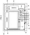
- FIG. 1is a schematic view of a liquid crystal display device according to an embodiment of the invention.
- FIG. 2is a cross-sectional view of a liquid crystal panel according to the embodiment of the invention.
- FIG. 3is a plan view that illustrates a first example of the liquid crystal panel according to the embodiment of the invention.
- FIG. 4is a plan view that illustrates a second example of the liquid crystal panel according to the embodiment of the invention.
- FIG. 5is a plan view that illustrates a third example of the liquid crystal panel according to the embodiment of the invention.
- FIG. 6is a cross-sectional view that illustrates an influence of static electricity according to an existing FFS mode liquid crystal display device.
- FIG. 7is a cross-sectional view that illustrates an influence of static electricity according to an existing FFS mode liquid crystal display device.
- electrostatic discharge resistancehas been considered on the basis of various evaluations. This will be described with reference to FIG. 6 and FIG. 7 illustrating the cross-sectional views around peripheral portions of a liquid crystal display device.
- a first substrate 100 Z and a second substrate 200 Zare adhered to each other by a seal 304 Z, and liquid crystal 302 Z is held between these substrates 100 Z, 200 Z.
- a circuit wiring group 104 Zis arranged on a support substrate 102 Z of the first substrate 100 Z, and an insulating film 114 Z is arranged so as to cover the circuit wiring group 104 Z. Note that the circuit wiring group 104 Z is schematically shown in the drawing.
- a translucent conductive film 208 Zis arranged on an outer surface of a support substrate 202 Z of the second substrate 200 Z, and this translucent conductive film 208 Z extends over the entire surface of the above outer surface, that is, to the outer periphery of the support substrate 202 Z, that is, to the outer periphery of the second substrate 200 z .
- the translucent conductive film 208 Zis formed so as to extend to the outer periphery of the second substrate 200 Z.
- FIG. 7is a schematic view illustrating a state of coupling using the graphic symbols of capacitors.
- the coupling with the translucent conductive film 208 Ztends to occur as the area of wiring pattern is increased, that is, the width and/or length, or the like, of wiring is increased. It is conceivable that, for example, the coupling tends to occur with a power supply wiring that has a wide line width for reducing a resistance.
- FIG. 1is a schematic view of a liquid crystal display device 10 according to the embodiment. Note that, for easily understanding the drawings, components that are shown in FIG. 1 and in the following drawings, when they are shown in the other drawings as well, are partially omitted.
- the liquid crystal display device 10is configured to include a liquid crystal panel 12 , a case 14 for the liquid crystal panel 12 , an FPC 16 , and an external circuit 18 .
- the liquid crystal panel 12is connected to the external circuit 18 through the FPC 16 .
- various wiring bodiesmay be used. The following will exemplify a case where the liquid crystal panel 12 uses an FFS mode.
- the liquid crystal panel 12may be any one of a transmissive type liquid crystal panel, a reflective type liquid crystal panel and a transflective type liquid crystal panel.
- FIG. 2is a cross-sectional view around an outer periphery of the liquid crystal panel 12 .
- the liquid crystal panel 12is configured to include a first substrate 100 , a second substrate 200 , liquid crystal 302 and a seal 304 .
- the substrates 100 , 200are opposed to each other with a predetermined gap formed therebetween, and are adhered to each other at the peripheral portions by the seal 304 .
- the liquid crystal 302is held in a casing that is formed of the substrates 100 , 200 and the seal 304 .
- the first substrate 100includes a support substrate 102 that is, for example, formed of a translucent substrate, such as glass, and is configured to include, on the inner surface side of the support substrate 102 , that is, on the side adjacent to the liquid crystal 302 , insulating films 110 , 112 , at least one common electrode 116 , pixel electrodes 118 , a peripheral circuit 150 , and an alignment layer (not shown).
- a support substrate 102that is, for example, formed of a translucent substrate, such as glass, and is configured to include, on the inner surface side of the support substrate 102 , that is, on the side adjacent to the liquid crystal 302 , insulating films 110 , 112 , at least one common electrode 116 , pixel electrodes 118 , a peripheral circuit 150 , and an alignment layer (not shown).
- the common electrode 116 and the pixel electrodes 118are paired electrodes that control the alignment of the liquid crystal 302 , that is, that drive the liquid crystal 302 .
- the common electrode 116is commonly provided for a plurality of pixels, and each of the pixel electrodes 118 is provided for each of the pixels. An electric potential corresponding to a display of each pixel is supplied to the pixel electrode 118 .
- the common electrode 116is provided for each of the pixels and then a common electric potential is supplied to the common electrode 116 . That is, the plurality of pixels are formed of the plurality of pixel electrodes 118 and the at least one common electrode 116 .
- the outermost pixels, arranged all around, or more number of pixelsmay possibly be used as dummy pixels that do not directly contribute to image display.
- the electrodes 116 , 118both are provided in the first substrate 100 , and the electrodes 116 , 118 are laminated through the insulating film 112 .
- the followingwill exemplify a case where the pixel electrodes 118 are arranged in an upper side layer, that is, on the side adjacent to the liquid crystal 302 ; however, the common electrodes 116 may be arranged in the upper side layer.
- Slits(not shown) are formed in each of the upper layer pixel electrodes 118 , and the alignment of the liquid crystal 302 is controlled by an electric field generated between the electrodes 116 , 118 through the slits.
- the electrodes 116 , 118are, for example, formed of a translucent conductive film, such as ITO (Indium Tin Oxide).
- the peripheral circuit 150is a circuit that is arranged outside the electrodes 116 , 118 and the pixel area 13 .
- the pixel area 13is an area in which a plurality of the pixels are arranged. In other words, the plurality of pixels are arranged in the pixel area 13 . Note that an area for the dummy pixels also included in the pixel area 13 .
- the peripheral circuit 150will be exemplified later.
- the insulating films 110 , 112are, for example, formed of silicon oxide, silicon nitride, or the like, and are laminated on the support substrate 102 . Note that, for easy description, it exemplifies a case where the insulating film 110 is located in a layer lower than the common electrode 116 , that is, the layer adjacent to the support substrate 102 , and the insulating film 112 is laminated on the insulating film 110 ; however, these insulating films 110 , 112 are collectively called as an insulating film 114 .
- the insulating films 110 , 112each may be a monolayer film or may be a multilayer film.
- the alignment layer(not shown) is arranged to cover the pixel electrodes 118 , and the alignment layer is treated with a rubbing process.
- FIG. 2exemplifies a case where the peripheral circuit 150 is in contact with the support substrate 102 and is covered with the insulating film 110 ; however, it may be configured so that the peripheral circuit 150 is embedded in the insulating film 114 formed of a multilayer film and is not in contact with the support substrate 102 .
- the second substrate 200includes a support substrate 202 that is, for example, formed of a translucent substrate, such as glass, and is configured to include, on the inner surface side of the support substrate 202 , that is, on the side adjacent to the liquid crystal 302 , a light shielding film 204 , a color filter 206 and an alignment layer (not shown) and to include, on the outer surface side of the support substrate 202 , that is, on the side opposite to the liquid crystal 302 , a translucent conductive film 208 .
- a support substrate 202that is, for example, formed of a translucent substrate, such as glass, and is configured to include, on the inner surface side of the support substrate 202 , that is, on the side adjacent to the liquid crystal 302 , a light shielding film 204 , a color filter 206 and an alignment layer (not shown) and to include, on the outer surface side of the support substrate 202 , that is, on the side opposite to the liquid crystal 302 , a translucent conductive film 208 .
- the support substrate 202is opposed to the first substrate 100 , and has a size to be opposed to be opposed to the electrodes 116 , 118 and the peripheral circuit 150 .
- the light shielding film 204is arranged on the support substrate 202 .
- the light shielding film 204extends over the entire surface on the support substrate 202 and has an opening at a position opposite each of the pixel electrodes 118 . Note that no opening is provided at a position opposite each of the dummy pixels.
- the light shielding film 204is, for example, formed a resin, or the like, containing black pigment.
- the color filter 206is arranged on the support substrate 202 and is provided in each opening portion of the light shielding film 204 so as to be opposed to the electrodes 116 , 118 .
- the alignment layer(not shown) is arranged to cover the light shielding film 204 and the color filter 206 , and the alignment layer is treated with a rubbing process.
- the translucent conductive film 208is arranged on the outer surface of the support substrate 202 and is opposed to the liquid crystal 302 and the electrodes 116 , 118 , and the like, through the substrate 202 . That is, the translucent conductive film 208 is provided in the second substrate 200 and is located on an opposite side to a surface that is in contact with the liquid crystal 302 .
- the translucent conductive film 208is maintained at an arbitrarily predetermined electric potential, for example, a ground electric potential, and releases static electricity, which enters from the outside of the panel toward the second substrate 200 , thus preventing electrostatic charge of the second substrate 200 . That is, the translucent conductive film 208 serves as a shielding film.
- the translucent conductive film 208may be provided without patterning (without any gaps), or, as long as the body portion 208 a achieves a shielding effect against static electricity, it may be patterned to form a mesh.
- the translucent conductive film 208is, for example, formed of ITO, or the like, and may be formed of any one of an inorganic material or an organic material.
- the translucent conductive film 208may be formed by a process, such as a sputtering process, a plasma CVD (Chemical Vapor Deposition) process, a spin coating process, and a printing process.
- the translucent conductive film 208has a resistivity (sheet resistance) of, for example, 105 ⁇ / ⁇ , which is preferably as low as possible.
- FIG. 3 to FIG. 5are plan views that illustrate liquid crystal panels 12 A to 12 C according to first example to third example. Note that, for avoiding complicated drawing, an area outside the pixel area 13 is shown wide, and a connection state, or the like, of a wiring is partially omitted from the drawing.
- the peripheral circuit 150is configured to include an H scanner 152 , a V scanner 154 , a V system circuit 156 , a circuit 158 , a COM wiring 162 , wirings 164 , 166 , and the like.
- the H scanner 152 and the V scanner 154are circuits for scanning pixels horizontally and vertically on a display screen.
- the V system circuit 156is, for example, a level shifter, and is connected to the V scanner 154 .
- the circuit 158is, for example, a control circuit, a signal processing circuit, a detection circuit, and the like. Here, the circuit 158 is connected to the scanners 152 , 154 .
- the COM wiring 162is a wiring that supplies an electric potential (common electric potential) to be applied to the common electrode 116 (see FIG. 2 ).
- the COM wiring 162extends from the end, which is connected to the FPC 16 , toward the pixel area 13 .
- the COM wiring 162extends from a portion near the pixel area 13 along three sides of the area 13 .
- the wiring 164is a control signal wiring for the V scanner 154 and extends from the end, which is connected to the FPC 16 , toward the V scanner 154 .
- the wiring 166is, for example, an input signal wiring to the V system circuit 156 and extends from the end, which is connected to the FPC 16 , toward the V system circuit 156 . Note that FIG. 3 exemplifies a case where the two wirings 166 are provided.
- the liquid crystal panel 12 Aincludes a dummy wiring 168 outside the pixel area 13 .
- the dummy wiring 168is arranged on the outer peripheral side of the substrate than the peripheral circuit 150 that is configured to include the scanners 152 , 154 , and the like.
- the dummy wiring 168is a wiring that is located on the outermost periphery among various wirings of the liquid crystal panel 12 A.
- the dummy wiring 168is not connected to the peripheral circuit 150 , that is, the dummy wiring 168 is provided independently of the peripheral circuit 150 in terms of circuit. According to the above arrangement and connection state, the dummy wiring 168 does not intersect with the peripheral circuit 150 .
- the dummy wiring 168surrounds the peripheral circuit 150 .
- the dummy wiring 168preferably avoids an intersection with the peripheral circuit 150 also at a portion connected to the FPC 16 .
- the dummy wiring 168does not constitute a closed path (closed loop) within the liquid crystal panel 12 A, and both ends of the dummy wiring 168 are pulled out to the portion connected to the FPC 16 .
- Both end portions of the dummy wiring 168are connected through the FPC 16 to the ground electric potential of the external circuit 18 .
- Both end portions of the dummy wiring 168may be connected to the ground electric potential through a resistance of 10 k ⁇ to 1 m ⁇ .
- the dummy wiring 168does not intersect with the peripheral circuit 150 . For this reason, static electricity entering the dummy wiring 168 is suppressed from being transmitted to the peripheral circuit 150 due to coupling. Thus, electrostatic discharge resistance is improved.
- the ground electric potentialmay possibly rise when static electricity enters the dummy wiring 168 .
- a signal, a power supply electric potential, or the liketo which a voltage value is set relatively to the ground electric potential as a reference, an influence of a rise in ground electric potential is suppressed. Therefore, electrostatic discharge resistance is improved in comparison with a case where the dummy wiring 168 is, for example, connected to the ground electric potential of the liquid crystal panel 12 A.
- the peripheral circuit 150is configured to include the H scanner 152 , the V scanner 154 , the V system circuit 156 , the circuit 158 , the COM wiring 162 , the wirings 164 , 166 , a power supply wiring 169 , and the like.
- the liquid crystal panel 12 Bincludes a dummy wiring 170 and protective resistances 180 . Note that the same reference numerals are assigned to the same or similar components described above, and a description there of is omitted.
- the power supply wiring 169is, for example, a wiring that supplies a power supply electric potential Vss, and extends from the end, which is connected to the FPC 16 , to be connected to the V system circuit 156 and the H scanner 152 .
- the electric potential Vssis, for example, supplied through the V system circuit 156 to the V scanner 154 and supplied through the H scanner 152 to the circuit 158 .
- the dummy wiring 170is connected through the resistance 180 to the power supply wiring 169 , and extends around the panel and then is connected through the other resistance 180 to the power supply wiring 169 again.
- the dummy wiring 170is located on the outermost periphery than various wirings of the peripheral circuit 150 .
- the dummy wiring 170surrounds the scanners 152 , 154 , the V system circuit 156 , the circuit 158 , and the like.
- the dummy wiring 170extends along the outer periphery of the substrate to form a closed loop in the liquid crystal panel 12 B.
- the protective resistances 180have a resistance value of, for example, 10 k ⁇ to 10 M ⁇ .
- the protective resistances 180may be, for example, formed by using a silicon film.
- the peripheral circuit 150includes, in addition to the above configuration exemplified in FIG. 4 , a power supply wiring 172 and a protective resistance 182 .
- the power supply wiring 172 and the protective resistance 182are arranged inside the above closed loop portion of the dummy wiring 17 in the liquid crystal panel 12 C. Note that the same reference numerals are assigned to the same or similar components described above, and a description thereof is omitted.
- the power supply wiring 172is a wiring that supplies a power supply electric potential used in the V scanner 154 and in the circuit 158 .
- the power supply electric potentialmay be an electric potential that is generated in the liquid crystal panel 12 C, or may be an electric potential that is supplied from the external circuit 18 (see FIG. 1 ), or the like.
- the power supply wiring 172passes through the V scanner 154 and extends along the outer periphery of the substrate, and then is connected through the protective resistance 182 to the circuit 158 .
- the protective resistance 182has a resistance value of, for example, 10 k ⁇ to 10 M ⁇ .
- the protective resistance 182may be, for example, formed by using a silicon film.
- the circuit 158 in the liquid crystal panel 12 Cuses the above power supply electric potential that is supplied by the power supply wiring 172 as a control signal.
- the circuit 158may be a signal processing circuit, a detection circuit, or the like, that is shared by the H scanner 152 and the V scanner 154 .
- the circuit 158is switched to a circuit for the V scanner 154 .
- the circuit 158is switched to a circuit for the H scanner 152 .
- the thus switchingmay be, for example, achieved by using a switching element, such as a MOS (Metal Oxide Semiconductor) transistor, and the power supply wiring 172 is connected to a control terminal of the switching element, that is, for example, the gate of the MOS transistor.
- a switching elementsuch as a MOS (Metal Oxide Semiconductor) transistor
- MOSMetal Oxide Semiconductor
- the protective resistance 182is connected in the power supply wiring 172 in a midway of the path from the V scanner 154 to the control terminal, and the protective resistance 182 is provided upstream of the control terminal.
- electrostatic discharge resistanceis reliably improved by connecting the protective resistances 180 , 182 to the wirings 170 , 172 , respectively.
- the wirings 170 , 172 to which the protective resistances 180 , 182 are connected and the dummy wiring 168may be variously combined, and, thereby, it is possible to further improve electrostatic discharge resistance. Furthermore, the dummy wiring 168 and the wirings 170 , 172 , to which the protective resistances 180 , 182 are connected, are effective against static electricity that enters the first substrate 100 without passing through the translucent conductive film 208 .
- the above descriptionexemplifies the FFS mode in which the electrodes 116 , 118 that drive the liquid crystal 302 are laminated through the insulating film 112 .
- itmay be configured as an IPS mode in which both electrodes 116 , 118 are arranged in the same layer (for example, on the insulating film 112 ).
- the electrodes 116 , 118 having a comb-shaped patternare arranged so that the comb-shaped portions are alternately meshed with each other.
- the above configured liquid crystal display device 10may be applied to a liquid crystal display device, such as a TN (Twisted Nematic) mode, in which the common electrode 116 is opposed to the pixel electrodes 118 through the liquid crystal 302 .
- TNTransmission Nematic
Landscapes
- Physics & Mathematics (AREA)
- Nonlinear Science (AREA)
- Mathematical Physics (AREA)
- Chemical & Material Sciences (AREA)
- Crystallography & Structural Chemistry (AREA)
- General Physics & Mathematics (AREA)
- Optics & Photonics (AREA)
- Engineering & Computer Science (AREA)
- Microelectronics & Electronic Packaging (AREA)
- Liquid Crystal (AREA)
- Geometry (AREA)
- Spectroscopy & Molecular Physics (AREA)
Abstract
Description
Claims (20)
Priority Applications (2)
| Application Number | Priority Date | Filing Date | Title |
|---|---|---|---|
| US18/490,038US12253770B2 (en) | 2006-12-27 | 2023-10-19 | Liquid crystal display device having improved electrostatic discharge resistance |
| US19/058,389US20250189852A1 (en) | 2006-12-27 | 2025-02-20 | Liquid crystal display device having improved electrostatic discharge resistance |
Applications Claiming Priority (8)
| Application Number | Priority Date | Filing Date | Title |
|---|---|---|---|
| JP2006352377AJP2008164787A (en) | 2006-12-27 | 2006-12-27 | Liquid crystal display device |
| JP2006-352377 | 2006-12-27 | ||
| US12/003,455US8830409B2 (en) | 2006-12-27 | 2007-12-26 | Liquid crystal display device having improved electrostatic discharge resistance |
| US14/447,243US9335594B2 (en) | 2006-12-27 | 2014-07-30 | Liquid crystal display device having improved electrostatic discharge resistance |
| US15/078,170US10001685B2 (en) | 2006-12-27 | 2016-03-23 | Liquid crystal display device having improved electrostatic discharge resistance |
| US15/984,873US11256151B2 (en) | 2006-12-27 | 2018-05-21 | Liquid crystal display device having improved electrostatic discharge resistance |
| US17/578,883US11835828B2 (en) | 2006-12-27 | 2022-01-19 | Liquid crystal display device having improved electrostatic discharge resistance |
| US18/490,038US12253770B2 (en) | 2006-12-27 | 2023-10-19 | Liquid crystal display device having improved electrostatic discharge resistance |
Related Parent Applications (1)
| Application Number | Title | Priority Date | Filing Date |
|---|---|---|---|
| US17/578,883ContinuationUS11835828B2 (en) | 2006-12-27 | 2022-01-19 | Liquid crystal display device having improved electrostatic discharge resistance |
Related Child Applications (1)
| Application Number | Title | Priority Date | Filing Date |
|---|---|---|---|
| US19/058,389ContinuationUS20250189852A1 (en) | 2006-12-27 | 2025-02-20 | Liquid crystal display device having improved electrostatic discharge resistance |
Publications (2)
| Publication Number | Publication Date |
|---|---|
| US20240045286A1 US20240045286A1 (en) | 2024-02-08 |
| US12253770B2true US12253770B2 (en) | 2025-03-18 |
Family
ID=39583368
Family Applications (8)
| Application Number | Title | Priority Date | Filing Date |
|---|---|---|---|
| US12/003,455Active2030-03-24US8830409B2 (en) | 2006-12-27 | 2007-12-26 | Liquid crystal display device having improved electrostatic discharge resistance |
| US14/447,243ActiveUS9335594B2 (en) | 2006-12-27 | 2014-07-30 | Liquid crystal display device having improved electrostatic discharge resistance |
| US15/078,170ActiveUS10001685B2 (en) | 2006-12-27 | 2016-03-23 | Liquid crystal display device having improved electrostatic discharge resistance |
| US15/984,873ActiveUS11256151B2 (en) | 2006-12-27 | 2018-05-21 | Liquid crystal display device having improved electrostatic discharge resistance |
| US16/776,120ActiveUS10935856B2 (en) | 2006-12-27 | 2020-01-29 | Display device with a translucent conductive film |
| US17/578,883Active2028-01-07US11835828B2 (en) | 2006-12-27 | 2022-01-19 | Liquid crystal display device having improved electrostatic discharge resistance |
| US18/490,038ActiveUS12253770B2 (en) | 2006-12-27 | 2023-10-19 | Liquid crystal display device having improved electrostatic discharge resistance |
| US19/058,389PendingUS20250189852A1 (en) | 2006-12-27 | 2025-02-20 | Liquid crystal display device having improved electrostatic discharge resistance |
Family Applications Before (6)
| Application Number | Title | Priority Date | Filing Date |
|---|---|---|---|
| US12/003,455Active2030-03-24US8830409B2 (en) | 2006-12-27 | 2007-12-26 | Liquid crystal display device having improved electrostatic discharge resistance |
| US14/447,243ActiveUS9335594B2 (en) | 2006-12-27 | 2014-07-30 | Liquid crystal display device having improved electrostatic discharge resistance |
| US15/078,170ActiveUS10001685B2 (en) | 2006-12-27 | 2016-03-23 | Liquid crystal display device having improved electrostatic discharge resistance |
| US15/984,873ActiveUS11256151B2 (en) | 2006-12-27 | 2018-05-21 | Liquid crystal display device having improved electrostatic discharge resistance |
| US16/776,120ActiveUS10935856B2 (en) | 2006-12-27 | 2020-01-29 | Display device with a translucent conductive film |
| US17/578,883Active2028-01-07US11835828B2 (en) | 2006-12-27 | 2022-01-19 | Liquid crystal display device having improved electrostatic discharge resistance |
Family Applications After (1)
| Application Number | Title | Priority Date | Filing Date |
|---|---|---|---|
| US19/058,389PendingUS20250189852A1 (en) | 2006-12-27 | 2025-02-20 | Liquid crystal display device having improved electrostatic discharge resistance |
Country Status (5)
| Country | Link |
|---|---|
| US (8) | US8830409B2 (en) |
| JP (1) | JP2008164787A (en) |
| KR (1) | KR20080063115A (en) |
| CN (1) | CN101211051B (en) |
| TW (1) | TWI383198B (en) |
Families Citing this family (27)
| Publication number | Priority date | Publication date | Assignee | Title |
|---|---|---|---|---|
| JP4789369B2 (en)* | 2001-08-08 | 2011-10-12 | 株式会社半導体エネルギー研究所 | Display device and electronic device |
| US7796224B2 (en)* | 2006-12-26 | 2010-09-14 | Sony Corporation | Liquid crystal display device |
| JP2008164787A (en)* | 2006-12-27 | 2008-07-17 | Epson Imaging Devices Corp | Liquid crystal display device |
| CN102089735A (en)* | 2008-08-07 | 2011-06-08 | 夏普株式会社 | Touch panel, display, and electronic device |
| JP5354545B2 (en)* | 2010-03-02 | 2013-11-27 | 株式会社ジャパンディスプレイ | Liquid crystal display device with capacitive touch panel |
| KR101307962B1 (en) | 2010-03-19 | 2013-09-12 | 엘지디스플레이 주식회사 | In-plane switching mode liquid crystal display device having touch sensing function and method of fabricating the same |
| KR101298234B1 (en) | 2010-03-19 | 2013-08-22 | 엘지디스플레이 주식회사 | In-plane switching mode liquid crystal display device having touch sensing function and method of fabricating the same |
| JP5409697B2 (en) | 2010-06-24 | 2014-02-05 | 株式会社ジャパンディスプレイ | Flat panel display |
| JP5533566B2 (en)* | 2010-10-29 | 2014-06-25 | 大日本印刷株式会社 | Color filter integrated touch panel sensor, display device with touch panel function, and method for manufacturing multi-faceted work substrate |
| JP5534452B2 (en)* | 2010-11-29 | 2014-07-02 | 大日本印刷株式会社 | Color filter integrated touch panel sensor, display device with touch panel function, and method for manufacturing multi-faceted work substrate |
| JP5708133B2 (en)* | 2011-03-29 | 2015-04-30 | セイコーエプソン株式会社 | Liquid crystal device and projection display device |
| JP2012208301A (en)* | 2011-03-29 | 2012-10-25 | Seiko Epson Corp | Liquid crystal device and projection type display device |
| JP2014224834A (en)* | 2011-09-06 | 2014-12-04 | シャープ株式会社 | Display device |
| CN102655148A (en)* | 2012-03-20 | 2012-09-05 | 京东方科技集团股份有限公司 | Thin film transistor (TFT) substrate, preparation method of TFT substrate, liquid crystal display (LCD) device and electronic paper display device |
| JP5795301B2 (en)* | 2012-11-28 | 2015-10-14 | 株式会社ジャパンディスプレイ | Display device and electronic device |
| CN103091877B (en)* | 2012-12-28 | 2015-08-26 | 亚世光电股份有限公司 | Antistatic LCD graphical design method |
| JP6148582B2 (en)* | 2013-09-10 | 2017-06-14 | 矢崎総業株式会社 | Vehicle instrument |
| JP6289163B2 (en) | 2014-02-27 | 2018-03-07 | 三菱電機株式会社 | Liquid crystal display |
| KR102611213B1 (en)* | 2016-06-22 | 2023-12-07 | 삼성디스플레이 주식회사 | Display device |
| CN106990588B (en)* | 2017-06-02 | 2019-10-01 | 厦门天马微电子有限公司 | A kind of display panel and display device |
| KR102552266B1 (en) | 2018-01-31 | 2023-07-07 | 삼성디스플레이 주식회사 | Display device |
| CN108983520B (en)* | 2018-09-29 | 2021-04-02 | 武汉华星光电技术有限公司 | Display panel with anti-electrostatic discharge |
| CN109283763B (en)* | 2018-11-16 | 2021-10-26 | 信利半导体有限公司 | Substrate structure, display panel and panel manufacturing method |
| CN110346994B (en)* | 2019-07-23 | 2022-07-08 | 昆山国显光电有限公司 | Array substrate and display panel |
| CN114167655A (en)* | 2020-09-11 | 2022-03-11 | Oppo广东移动通信有限公司 | Electrochromic modules, cover assemblies and electronic equipment |
| KR20240127796A (en)* | 2023-02-16 | 2024-08-23 | 삼성전자주식회사 | Display apparatus |
| KR20250111955A (en)* | 2024-01-16 | 2025-07-23 | 엘지디스플레이 주식회사 | Display apparatus and display panel |
Citations (121)
| Publication number | Priority date | Publication date | Assignee | Title |
|---|---|---|---|---|
| US5185601A (en) | 1990-01-11 | 1993-02-09 | Matsushita Electric Industrial Co., Ltd. | Active matrix liquid crystal display apparatus and method of producing the same |
| US5285301A (en) | 1991-03-15 | 1994-02-08 | Hitachi, Ltd. | Liquid crystal display device having peripheral dummy lines |
| JPH06186553A (en) | 1992-12-18 | 1994-07-08 | Hitachi Ltd | Liquid crystal display device |
| JPH0741586U (en) | 1993-12-29 | 1995-07-21 | カシオ計算機株式会社 | Display drive |
| JPH09105918A (en) | 1995-10-12 | 1997-04-22 | Hitachi Ltd | Liquid crystal display |
| JPH1020338A (en) | 1996-07-02 | 1998-01-23 | Hitachi Ltd | Liquid crystal display |
| JPH1048663A (en) | 1996-08-06 | 1998-02-20 | Toshiba Corp | Liquid crystal display |
| US5781261A (en) | 1995-07-17 | 1998-07-14 | Hitachi, Ltd. | Active matrix type LCD having light shield layers and counter electrodes made of the same material |
| JPH10268278A (en) | 1997-03-27 | 1998-10-09 | Sony Corp | Liquid crystal display device |
| CN1198835A (en) | 1996-06-11 | 1998-11-11 | 住友大阪水泥株式会社 | Transparent conductive film, low-reflectivity transparent conductive film, and display |
| US5859683A (en) | 1995-09-29 | 1999-01-12 | Sharp Kabushiki Kaisha | Transmissive liquid crystal display apparatus and method for producing the same |
| JPH11119252A (en) | 1997-10-16 | 1999-04-30 | Hitachi Ltd | Active matrix liquid crystal display |
| US5953092A (en) | 1996-10-28 | 1999-09-14 | Frontec Incorporated | Liquid crystal device with split pixel electrodes and with intermediate electrodes used for bisecting each of the pixel regions |
| JPH11282011A (en) | 1998-03-30 | 1999-10-15 | Seiko Epson Corp | Active matrix substrate manufacturing method and liquid crystal display device |
| US5995189A (en) | 1995-12-21 | 1999-11-30 | Semiconductor Energy Laboratory Co., Ltd. | Liquid-crystal display device |
| US6097467A (en) | 1996-08-05 | 2000-08-01 | Nec Corporation | Latitudinal LCD with cylindrical and eliptical spacers at intersection of signal and gate lines |
| US6111625A (en) | 1996-09-02 | 2000-08-29 | Hitachi, Ltd. | Active matrix Type liquid crystal display device |
| US6124917A (en) | 1996-12-19 | 2000-09-26 | Sharp Kabushiki Kaisha | LCD device having adhesion reinforcing portion in a part of insulator contacting seal |
| JP2000349239A (en) | 1990-04-24 | 2000-12-15 | Seiko Epson Corp | Semiconductor chip package and display device using the same |
| JP2001021918A (en) | 1999-07-07 | 2001-01-26 | Hitachi Ltd | Liquid crystal display |
| US6188458B1 (en) | 1995-09-28 | 2001-02-13 | Sharp Kabushiki Kaisha | Liquid crystal display device with thick interlayer insulating film under pixel electrode |
| US6201590B1 (en) | 1995-03-17 | 2001-03-13 | Hitachi, Ltd. | Liquid crystal display device with double-layered structure for gate line and/or data line |
| US6208399B1 (en) | 1997-04-11 | 2001-03-27 | Hitachi, Ltd. | Liquid crystal display device |
| US6219115B1 (en) | 1998-08-05 | 2001-04-17 | Hitachi, Ltd. | Liquid crystal display device |
| US6222595B1 (en) | 1996-04-01 | 2001-04-24 | Semiconductor Energy Laboratory Co., Ltd. | TFT-LCD having pixel electrode overlapping scan and data lines except at the intersection of lines |
| US6233034B1 (en) | 1997-12-29 | 2001-05-15 | Hyundai Electronics Industries Co., Ltd. | Liquid crystal display and fabrication method |
| US6259502B1 (en) | 1997-07-12 | 2001-07-10 | Lg Electronics Inc. | In-plane switching mode liquid crystal display device having a common electrode on the passivation layer |
| US6262702B1 (en) | 1997-10-31 | 2001-07-17 | Seiko Epson Corporation | Electro-optical device and electronic apparatus |
| US6266118B1 (en) | 1998-05-29 | 2001-07-24 | Hyundai Electronics Industries Co., Ltd. | Liquid crystal display of high aperture ratio and high transmittance having multi-domain having transparent conductive pixel and counter electrodes on the same substrate |
| US6281953B1 (en) | 1998-08-24 | 2001-08-28 | Hyundai Electronics Industries Co., Ltd. | Liquid crystal display having high aperture ratio and high transmittance and method of manufacturing the same |
| US6292237B1 (en) | 1998-07-16 | 2001-09-18 | Alps Electric Co., Ltd. | Active-matrix liquid-crystal display device and substrate therefor |
| US6297867B1 (en) | 1997-11-12 | 2001-10-02 | Nec Corporation | Wide view angle LCD operable in IPS mode which uses a pixel electrode as a shield to prevent disturbances in the electric field of a display pixel portion of the LCD |
| US20010030717A1 (en) | 2000-01-07 | 2001-10-18 | Hitachi, Ltd. | Liquid crystal display device |
| US20010046027A1 (en) | 1999-09-03 | 2001-11-29 | Ya-Hsiang Tai | Liquid crystal display having stripe-shaped common electrodes formed above plate-shaped pixel electrodes |
| US20010055085A1 (en)* | 1997-09-26 | 2001-12-27 | Yushi Jinno | Display apparatus and method for manufacturing the same |
| US6335770B1 (en) | 1997-07-22 | 2002-01-01 | Lg. Philips Lcd Co., Ltd. | In-plane switching mode LCD with specific arrangement of common bus line, data electrode, and common electrode |
| US6341003B1 (en) | 1998-01-23 | 2002-01-22 | Hitachi, Ltd. | Liquid crystal display device in which the pixel electrode crosses the counter electrode |
| US6346932B1 (en) | 1996-03-14 | 2002-02-12 | Seiko Epson Corporation | Liquid crystal device and electronic equipment |
| US6356330B1 (en) | 1998-10-27 | 2002-03-12 | Hitachi, Ltd. | Active matrix liquid crystal display device |
| US6392622B1 (en) | 1998-02-19 | 2002-05-21 | Seiko Epson Corporation | Active-matrix substrate, electro-optical device, method for manufacturing active-matrix substrate, and electronic equipment |
| US6404475B1 (en) | 1998-08-12 | 2002-06-11 | Hitachi, Ltd. | Liquid crystal display device having two regions in a pixel with structural difference in insulating layer |
| US6411360B1 (en) | 1999-06-18 | 2002-06-25 | Hitachi, Ltd. | Inplane switching type liquid crystal display with alignment layer formed on columnar spacer directly |
| JP2002215059A (en) | 2001-01-18 | 2002-07-31 | Seiko Epson Corp | Electro-optical device |
| US6441876B1 (en) | 2000-05-31 | 2002-08-27 | Sony Corporation | Liquid crystal display device and method of producing the same |
| US6445435B1 (en) | 1998-01-23 | 2002-09-03 | Lg. Philips Lcd Co., Ltd. | In-plane switching mode liquid cystal display device having common electrode on passivation layer |
| US6449026B1 (en) | 1999-06-25 | 2002-09-10 | Hyundai Display Technology Inc. | Fringe field switching liquid crystal display and method for manufacturing the same |
| US20020126231A1 (en) | 1996-02-13 | 2002-09-12 | Semiconductor Energy Laboratory Co., Ltd., A Japanese Corporation | Electro-optical device and manufacturing method thereof |
| US6462800B1 (en) | 1999-06-30 | 2002-10-08 | Hyundai Display Technology Inc. | Electrode contact structure for a liquid crystal display device and manufacturing method thereof |
| US6466290B2 (en) | 1999-12-22 | 2002-10-15 | Hyundai Display Technology Inc. | Fringe field switching mode LCD |
| US6469765B1 (en) | 1999-06-16 | 2002-10-22 | Nec Corporation | Liquid crystal display and method of performing display operation |
| JP2002357807A (en) | 2001-05-31 | 2002-12-13 | Matsushita Electric Ind Co Ltd | Liquid crystal display |
| US6532053B2 (en) | 1996-12-18 | 2003-03-11 | Hitachi, Ltd. | Transverse electric field system liquid crystal display device suitable for improving aperture ratio |
| JP2003075860A (en) | 2001-09-05 | 2003-03-12 | Hitachi Ltd | Liquid crystal display |
| US6549260B1 (en) | 1999-03-26 | 2003-04-15 | Nec Corporation | Liquid crystal display device of latitudinal electric field type having protruded spacer covers common line |
| US6577368B1 (en) | 1997-11-03 | 2003-06-10 | Samsung Electronics Co., Ltd. | IPS-LCD having a third electrode having aperture and formed on counter substrate |
| US6583845B1 (en) | 2000-02-23 | 2003-06-24 | Lg.Philips Lcd Co., Ltd. | Liquid crystal display device and method of fabricating the same |
| TW200301567A (en) | 2001-12-28 | 2003-07-01 | Fujitsu Display Tech | Liquid crystal display device and method of manufacturing the same |
| US6597414B1 (en) | 1999-02-26 | 2003-07-22 | Nec Lcd Technologies, Ltd. | Horizontal electric-field type LCD device |
| US6650389B1 (en) | 1998-09-14 | 2003-11-18 | Nec Lcd Technologies, Ltd. | Liquid crystal display device and method of manufacturing the same |
| US20030218593A1 (en) | 2002-03-28 | 2003-11-27 | Seiko Epson Corporation | Electrooptic device, driving method therefor, electronic device, and projection display device |
| JP2004004754A (en) | 1996-03-14 | 2004-01-08 | Seiko Epson Corp | Liquid crystal device and electronic equipment using the same |
| US20040036833A1 (en) | 2002-08-23 | 2004-02-26 | Sharp Kabushiki Kaisha | Flexible substrate, LCD module using same, and manufacturing method of same |
| US20040145695A1 (en) | 2003-01-15 | 2004-07-29 | Nagatoshi Kurahashi | Liquid crystal display device |
| US6771342B1 (en) | 1996-03-05 | 2004-08-03 | Semiconductor Energy Laboratory Co., Ltd. | Liquid crystal display device and display device |
| US20040183977A1 (en) | 2003-03-19 | 2004-09-23 | Nec Lcd Technologies, Ltd | Liquid crystal display device and method of fabricating the same |
| US6798486B2 (en) | 1999-04-14 | 2004-09-28 | Hitachi, Ltd. | Liquid crystal display device with spacers formed on a planarizing film disposed over color filters |
| CN1540396A (en) | 2003-04-25 | 2004-10-27 | 胜华科技股份有限公司 | Method and device for arranging conductive metal wires of display panel with point discharge |
| US20040239641A1 (en) | 2001-09-06 | 2004-12-02 | Kazuhiko Takahata | Touch panel having high durability |
| US6833897B2 (en) | 2002-04-19 | 2004-12-21 | Hannstar Display Corp. | IPS-LCD device with a color filter formed on an array substrate |
| JP2005003816A (en) | 2003-06-10 | 2005-01-06 | Seiko Epson Corp | Electro-optical device, driving method of electro-optical device, and electronic apparatus |
| US20050046619A1 (en) | 2003-08-28 | 2005-03-03 | Sharp Kabushiki Kaisha | Driving circuit for display device, and display device |
| US20050046779A1 (en) | 2002-05-17 | 2005-03-03 | Advanced Display Inc. | Liquid crystal display device |
| JP2005062472A (en) | 2003-08-12 | 2005-03-10 | Kyodo Printing Co Ltd | Liquid crystal display device, portable medium, and method for manufacturing electrode substrate of liquid crystal display device |
| US20050099402A1 (en) | 2003-11-06 | 2005-05-12 | Akira Nakanishi | Touch panel and liquid crystal display apparatus using the same |
| US20050105034A1 (en) | 2003-11-19 | 2005-05-19 | Kikuo Ono | Liquid crystal display device |
| US6897931B2 (en) | 2002-11-30 | 2005-05-24 | Lg.Philips Lcd Co., Ltd. | In-plane switching mode liquid crystal display device and method for fabricating the same |
| US20050158665A1 (en) | 2004-01-16 | 2005-07-21 | Semiconductor Energy Laboratory Co., Ltd. | Substrate having film pattern and manufacturing method of the same, manufacturing method of semiconductor device, liquid crystal television, and EL television |
| CN1645190A (en) | 2004-01-20 | 2005-07-27 | 夏普株式会社 | Display element and display apparatus |
| US20050162605A1 (en) | 2003-06-02 | 2005-07-28 | Seiko Epson Corporation | Electro-optical device and electronic apparatus comprising the same |
| TW200529706A (en) | 2003-11-28 | 2005-09-01 | Sony Corp | Electronic circuit wiring and display device |
| CN1670759A (en) | 2004-03-19 | 2005-09-21 | 统宝光电股份有限公司 | Touch panel, display system and electronic device using same |
| US20050259210A1 (en) | 2004-05-10 | 2005-11-24 | Min-Jic Lee | Plane switching mode liquid crystal display device having improved contrast ratio |
| US20060002045A1 (en) | 2004-07-05 | 2006-01-05 | Seiko Epson Corporation | Semiconductor device, display device, and electronic apparatus |
| US20060061268A1 (en) | 2002-05-28 | 2006-03-23 | Seiko Epson Corporation | Light-emitting device with improved brightness control and narrow frame and electronic apparatus with the light-emitting device |
| US20060103412A1 (en) | 2004-10-29 | 2006-05-18 | Yohei Kimura | Display device |
| CN2789801Y (en) | 2005-04-21 | 2006-06-21 | 比亚迪股份有限公司 | Liquid crystal displaying device with antielectrostatic structure |
| US20060170854A1 (en) | 2005-02-01 | 2006-08-03 | Samsung Electronics Co., Ltd. | Liquid crystal display and method of fabricating the same |
| US20060267913A1 (en)* | 2005-05-27 | 2006-11-30 | Seiko Epson Corporation | Electro-optical device and electronic apparatus having the same |
| US7148944B2 (en) | 2002-05-17 | 2006-12-12 | Toshiba Matsushita Display Technology Co., Ltd. | Bendable display apparatus and method of manufacturing the same |
| US7173281B2 (en) | 1999-07-06 | 2007-02-06 | Semiconductor Energy Laboratory Co., Ltd. | Semiconductor device and method of fabricating the same |
| US20070040816A1 (en) | 2005-08-17 | 2007-02-22 | Nec Lcd Technologies, Ltd. | Display apparatus, electronics device equipped with display apparatus, and manufacturing method thereof |
| US20070046844A1 (en)* | 2005-08-24 | 2007-03-01 | Seiko Epson Corporation | Electro-optical device and electronic apparatus including the same |
| JP2007065157A (en) | 2005-08-30 | 2007-03-15 | Seiko Epson Corp | Electro-optical device and electronic apparatus including the same |
| US20070080624A1 (en) | 2004-07-30 | 2007-04-12 | Kaoru Koiwa | Display device |
| US20070171319A1 (en) | 2006-01-26 | 2007-07-26 | Sanyo Epson Imaging Devices Corporation | Liquid crystal apparatus and electronic device |
| US20070200992A1 (en) | 2006-02-27 | 2007-08-30 | Chul-Ho Kim | LCD display device having dummy pixels |
| US7282091B2 (en) | 2003-06-04 | 2007-10-16 | Fujifilm Corporation | Cellulose acylate-based dope, cellulose acylate film, and method of producing a cellulose acylate film |
| JP2007293155A (en) | 2006-04-27 | 2007-11-08 | Epson Imaging Devices Corp | Liquid crystal display device |
| US20080007679A1 (en) | 2006-07-07 | 2008-01-10 | Hitachi Displays, Ltd. | Transflective liquid crystal display device |
| US20080007666A1 (en) | 2006-07-07 | 2008-01-10 | Shintaro Takeda | Optically isotropic liquid crystal materials and display apparatus using the same |
| US20080018636A1 (en)* | 2006-07-18 | 2008-01-24 | Jong-Woong Chang | Driver chip, display device and method of repair |
| US7327411B2 (en) | 2003-12-16 | 2008-02-05 | Samsung Electronics Co., Ltd. | Driver chip and display apparatus having the same |
| US7372680B2 (en) | 2003-11-03 | 2008-05-13 | Samsung Sdi Co., Ltd. | Electromagnetic field preventing and protecting circuit of organic electroluminescent display device having a separated structure |
| US20080137020A1 (en) | 2006-12-08 | 2008-06-12 | Epson Imaging Devices Corporation | Liquid crystal apparatus and electronic apparatus |
| US20080158453A1 (en) | 2006-12-27 | 2008-07-03 | Epson Imaging Devices Corporation | Liquid crystal display device |
| US7460203B2 (en) | 2005-10-14 | 2008-12-02 | Lg.Philips Lcd Co., Ltd | Liquid crystal display device |
| US20090026932A1 (en) | 2007-07-23 | 2009-01-29 | Won-Kyu Kwak | Organic light emitting display and method of manufacturing the same |
| US7495648B2 (en) | 2003-12-11 | 2009-02-24 | Lg Display Co., Ltd. | Liquid crystal display device |
| US7551256B1 (en) | 1997-05-19 | 2009-06-23 | Lg Display Co., Ltd. | In-plane switching mode liquid crystal display device |
| CN100507693C (en) | 2001-10-15 | 2009-07-01 | 株式会社日立制作所 | Liquid crystal display device |
| US20100006838A1 (en) | 2006-07-31 | 2010-01-14 | Masahiro Yoshida | Active matrix substrate, display device, and active matrix substrate inspecting method |
| US7742140B2 (en) | 2004-12-28 | 2010-06-22 | Lg. Display Co., Ltd. | In-plane switching mode liquid crystal display device with common voltage transmission wire |
| US7839476B2 (en) | 2006-05-31 | 2010-11-23 | Hitachi Displays, Ltd. | Display device |
| US8081148B2 (en) | 2006-11-07 | 2011-12-20 | Hitachi Displays, Ltd. | Display device |
| US8652766B2 (en) | 2010-10-05 | 2014-02-18 | Hitachi Displays, Ltd. | Manufacturing method of display device |
| US8665191B2 (en) | 2007-10-24 | 2014-03-04 | Samsung Display Co., Ltd. | Organic light emitting display |
| US8830429B2 (en) | 2009-09-09 | 2014-09-09 | Japan Display Inc. | Liquid crystal display device |
| US8908116B2 (en) | 2010-10-29 | 2014-12-09 | Japan Display Inc. | Liquid crystal display device |
| US20150116623A1 (en) | 2013-10-31 | 2015-04-30 | Japan Display Inc. | Liquid crystal display device |
| US20150138476A1 (en) | 2013-11-18 | 2015-05-21 | Japan Display Inc. | Liquid crystal display device |
| US9285636B2 (en) | 2008-05-27 | 2016-03-15 | Japan Display Inc. | Liquid crystal display device |
Family Cites Families (7)
| Publication number | Priority date | Publication date | Assignee | Title |
|---|---|---|---|---|
| JPH0741586A (en) | 1993-05-21 | 1995-02-10 | Dainippon Ink & Chem Inc | Method of manufacturing foam |
| JP2005128040A (en)* | 2003-10-21 | 2005-05-19 | Hitachi Displays Ltd | Display device |
| JP4214946B2 (en)* | 2004-04-20 | 2009-01-28 | セイコーエプソン株式会社 | Electro-optical device and electronic apparatus |
| TWI265341B (en)* | 2004-12-31 | 2006-11-01 | Benq Corp | LCD apparatus with electrostatic discharge protection member |
| JP2007139967A (en)* | 2005-11-16 | 2007-06-07 | Canon Inc | Current-driven device and display device |
| JP4448834B2 (en)* | 2006-04-25 | 2010-04-14 | セイコーエプソン株式会社 | Electro-optical device and electronic apparatus including the same |
| US7839083B2 (en)* | 2007-02-08 | 2010-11-23 | Seiko Epson Corporation | Light emitting device and electronic apparatus |
- 2006
- 2006-12-27JPJP2006352377Apatent/JP2008164787A/ennot_activeWithdrawn
- 2007
- 2007-12-13TWTW096147586Apatent/TWI383198B/enactive
- 2007-12-26KRKR1020070137222Apatent/KR20080063115A/ennot_activeCeased
- 2007-12-26CNCN2007103011949Apatent/CN101211051B/enactiveActive
- 2007-12-26USUS12/003,455patent/US8830409B2/enactiveActive
- 2014
- 2014-07-30USUS14/447,243patent/US9335594B2/enactiveActive
- 2016
- 2016-03-23USUS15/078,170patent/US10001685B2/enactiveActive
- 2018
- 2018-05-21USUS15/984,873patent/US11256151B2/enactiveActive
- 2020
- 2020-01-29USUS16/776,120patent/US10935856B2/enactiveActive
- 2022
- 2022-01-19USUS17/578,883patent/US11835828B2/enactiveActive
- 2023
- 2023-10-19USUS18/490,038patent/US12253770B2/enactiveActive
- 2025
- 2025-02-20USUS19/058,389patent/US20250189852A1/enactivePending
Patent Citations (132)
| Publication number | Priority date | Publication date | Assignee | Title |
|---|---|---|---|---|
| US5185601A (en) | 1990-01-11 | 1993-02-09 | Matsushita Electric Industrial Co., Ltd. | Active matrix liquid crystal display apparatus and method of producing the same |
| JP2000349239A (en) | 1990-04-24 | 2000-12-15 | Seiko Epson Corp | Semiconductor chip package and display device using the same |
| US5285301A (en) | 1991-03-15 | 1994-02-08 | Hitachi, Ltd. | Liquid crystal display device having peripheral dummy lines |
| JPH06186553A (en) | 1992-12-18 | 1994-07-08 | Hitachi Ltd | Liquid crystal display device |
| JPH0741586U (en) | 1993-12-29 | 1995-07-21 | カシオ計算機株式会社 | Display drive |
| US6201590B1 (en) | 1995-03-17 | 2001-03-13 | Hitachi, Ltd. | Liquid crystal display device with double-layered structure for gate line and/or data line |
| US5781261A (en) | 1995-07-17 | 1998-07-14 | Hitachi, Ltd. | Active matrix type LCD having light shield layers and counter electrodes made of the same material |
| US6188458B1 (en) | 1995-09-28 | 2001-02-13 | Sharp Kabushiki Kaisha | Liquid crystal display device with thick interlayer insulating film under pixel electrode |
| US5859683A (en) | 1995-09-29 | 1999-01-12 | Sharp Kabushiki Kaisha | Transmissive liquid crystal display apparatus and method for producing the same |
| JPH09105918A (en) | 1995-10-12 | 1997-04-22 | Hitachi Ltd | Liquid crystal display |
| US5995189A (en) | 1995-12-21 | 1999-11-30 | Semiconductor Energy Laboratory Co., Ltd. | Liquid-crystal display device |
| US20020126231A1 (en) | 1996-02-13 | 2002-09-12 | Semiconductor Energy Laboratory Co., Ltd., A Japanese Corporation | Electro-optical device and manufacturing method thereof |
| US6771342B1 (en) | 1996-03-05 | 2004-08-03 | Semiconductor Energy Laboratory Co., Ltd. | Liquid crystal display device and display device |
| US6473067B2 (en) | 1996-03-14 | 2002-10-29 | Seiko Epson Corporation | Liquid crystal device and electronic equipment technical field |
| US6657608B2 (en) | 1996-03-14 | 2003-12-02 | Seiko Epson Corporation | Liquid crystal device and electronic equipment |
| JP2004004754A (en) | 1996-03-14 | 2004-01-08 | Seiko Epson Corp | Liquid crystal device and electronic equipment using the same |
| US6346932B1 (en) | 1996-03-14 | 2002-02-12 | Seiko Epson Corporation | Liquid crystal device and electronic equipment |
| US6222595B1 (en) | 1996-04-01 | 2001-04-24 | Semiconductor Energy Laboratory Co., Ltd. | TFT-LCD having pixel electrode overlapping scan and data lines except at the intersection of lines |
| CN1198835A (en) | 1996-06-11 | 1998-11-11 | 住友大阪水泥株式会社 | Transparent conductive film, low-reflectivity transparent conductive film, and display |
| US6143418A (en) | 1996-06-11 | 2000-11-07 | Sumitomo Osaka Cement Co., Ltd. | Transparent conductive film, low-reflectivity transparent conductive film, and display device |
| JPH1020338A (en) | 1996-07-02 | 1998-01-23 | Hitachi Ltd | Liquid crystal display |
| US6097467A (en) | 1996-08-05 | 2000-08-01 | Nec Corporation | Latitudinal LCD with cylindrical and eliptical spacers at intersection of signal and gate lines |
| JPH1048663A (en) | 1996-08-06 | 1998-02-20 | Toshiba Corp | Liquid crystal display |
| US6111625A (en) | 1996-09-02 | 2000-08-29 | Hitachi, Ltd. | Active matrix Type liquid crystal display device |
| US5953092A (en) | 1996-10-28 | 1999-09-14 | Frontec Incorporated | Liquid crystal device with split pixel electrodes and with intermediate electrodes used for bisecting each of the pixel regions |
| US6532053B2 (en) | 1996-12-18 | 2003-03-11 | Hitachi, Ltd. | Transverse electric field system liquid crystal display device suitable for improving aperture ratio |
| US6124917A (en) | 1996-12-19 | 2000-09-26 | Sharp Kabushiki Kaisha | LCD device having adhesion reinforcing portion in a part of insulator contacting seal |
| JPH10268278A (en) | 1997-03-27 | 1998-10-09 | Sony Corp | Liquid crystal display device |
| US6208399B1 (en) | 1997-04-11 | 2001-03-27 | Hitachi, Ltd. | Liquid crystal display device |
| US20010009447A1 (en) | 1997-04-11 | 2001-07-26 | Masuyuki Ohta | Liquid crystal display device |
| US7551256B1 (en) | 1997-05-19 | 2009-06-23 | Lg Display Co., Ltd. | In-plane switching mode liquid crystal display device |
| US6259502B1 (en) | 1997-07-12 | 2001-07-10 | Lg Electronics Inc. | In-plane switching mode liquid crystal display device having a common electrode on the passivation layer |
| US6335770B1 (en) | 1997-07-22 | 2002-01-01 | Lg. Philips Lcd Co., Ltd. | In-plane switching mode LCD with specific arrangement of common bus line, data electrode, and common electrode |
| US20010055085A1 (en)* | 1997-09-26 | 2001-12-27 | Yushi Jinno | Display apparatus and method for manufacturing the same |
| JPH11119252A (en) | 1997-10-16 | 1999-04-30 | Hitachi Ltd | Active matrix liquid crystal display |
| US6262702B1 (en) | 1997-10-31 | 2001-07-17 | Seiko Epson Corporation | Electro-optical device and electronic apparatus |
| US6577368B1 (en) | 1997-11-03 | 2003-06-10 | Samsung Electronics Co., Ltd. | IPS-LCD having a third electrode having aperture and formed on counter substrate |
| US6297867B1 (en) | 1997-11-12 | 2001-10-02 | Nec Corporation | Wide view angle LCD operable in IPS mode which uses a pixel electrode as a shield to prevent disturbances in the electric field of a display pixel portion of the LCD |
| US6233034B1 (en) | 1997-12-29 | 2001-05-15 | Hyundai Electronics Industries Co., Ltd. | Liquid crystal display and fabrication method |
| US6445435B1 (en) | 1998-01-23 | 2002-09-03 | Lg. Philips Lcd Co., Ltd. | In-plane switching mode liquid cystal display device having common electrode on passivation layer |
| US6341003B1 (en) | 1998-01-23 | 2002-01-22 | Hitachi, Ltd. | Liquid crystal display device in which the pixel electrode crosses the counter electrode |
| US6392622B1 (en) | 1998-02-19 | 2002-05-21 | Seiko Epson Corporation | Active-matrix substrate, electro-optical device, method for manufacturing active-matrix substrate, and electronic equipment |
| JPH11282011A (en) | 1998-03-30 | 1999-10-15 | Seiko Epson Corp | Active matrix substrate manufacturing method and liquid crystal display device |
| US6266118B1 (en) | 1998-05-29 | 2001-07-24 | Hyundai Electronics Industries Co., Ltd. | Liquid crystal display of high aperture ratio and high transmittance having multi-domain having transparent conductive pixel and counter electrodes on the same substrate |
| US6292237B1 (en) | 1998-07-16 | 2001-09-18 | Alps Electric Co., Ltd. | Active-matrix liquid-crystal display device and substrate therefor |
| US6219115B1 (en) | 1998-08-05 | 2001-04-17 | Hitachi, Ltd. | Liquid crystal display device |
| US6404475B1 (en) | 1998-08-12 | 2002-06-11 | Hitachi, Ltd. | Liquid crystal display device having two regions in a pixel with structural difference in insulating layer |
| US6281953B1 (en) | 1998-08-24 | 2001-08-28 | Hyundai Electronics Industries Co., Ltd. | Liquid crystal display having high aperture ratio and high transmittance and method of manufacturing the same |
| US6650389B1 (en) | 1998-09-14 | 2003-11-18 | Nec Lcd Technologies, Ltd. | Liquid crystal display device and method of manufacturing the same |
| US6356330B1 (en) | 1998-10-27 | 2002-03-12 | Hitachi, Ltd. | Active matrix liquid crystal display device |
| US6597414B1 (en) | 1999-02-26 | 2003-07-22 | Nec Lcd Technologies, Ltd. | Horizontal electric-field type LCD device |
| US6549260B1 (en) | 1999-03-26 | 2003-04-15 | Nec Corporation | Liquid crystal display device of latitudinal electric field type having protruded spacer covers common line |
| US6798486B2 (en) | 1999-04-14 | 2004-09-28 | Hitachi, Ltd. | Liquid crystal display device with spacers formed on a planarizing film disposed over color filters |
| US6469765B1 (en) | 1999-06-16 | 2002-10-22 | Nec Corporation | Liquid crystal display and method of performing display operation |
| US6411360B1 (en) | 1999-06-18 | 2002-06-25 | Hitachi, Ltd. | Inplane switching type liquid crystal display with alignment layer formed on columnar spacer directly |
| US6449026B1 (en) | 1999-06-25 | 2002-09-10 | Hyundai Display Technology Inc. | Fringe field switching liquid crystal display and method for manufacturing the same |
| US6462800B1 (en) | 1999-06-30 | 2002-10-08 | Hyundai Display Technology Inc. | Electrode contact structure for a liquid crystal display device and manufacturing method thereof |
| US7173281B2 (en) | 1999-07-06 | 2007-02-06 | Semiconductor Energy Laboratory Co., Ltd. | Semiconductor device and method of fabricating the same |
| JP2001021918A (en) | 1999-07-07 | 2001-01-26 | Hitachi Ltd | Liquid crystal display |
| US20010046027A1 (en) | 1999-09-03 | 2001-11-29 | Ya-Hsiang Tai | Liquid crystal display having stripe-shaped common electrodes formed above plate-shaped pixel electrodes |
| US6466290B2 (en) | 1999-12-22 | 2002-10-15 | Hyundai Display Technology Inc. | Fringe field switching mode LCD |
| US20010030717A1 (en) | 2000-01-07 | 2001-10-18 | Hitachi, Ltd. | Liquid crystal display device |
| US6583845B1 (en) | 2000-02-23 | 2003-06-24 | Lg.Philips Lcd Co., Ltd. | Liquid crystal display device and method of fabricating the same |
| US6441876B1 (en) | 2000-05-31 | 2002-08-27 | Sony Corporation | Liquid crystal display device and method of producing the same |
| JP2002215059A (en) | 2001-01-18 | 2002-07-31 | Seiko Epson Corp | Electro-optical device |
| JP2002357807A (en) | 2001-05-31 | 2002-12-13 | Matsushita Electric Ind Co Ltd | Liquid crystal display |
| JP2003075860A (en) | 2001-09-05 | 2003-03-12 | Hitachi Ltd | Liquid crystal display |
| US20040239641A1 (en) | 2001-09-06 | 2004-12-02 | Kazuhiko Takahata | Touch panel having high durability |
| CN100507693C (en) | 2001-10-15 | 2009-07-01 | 株式会社日立制作所 | Liquid crystal display device |
| US20030137621A1 (en) | 2001-12-28 | 2003-07-24 | Fujitsu Display Technologies Corporation | Liquid crystal display device and method of manufacturing the same |
| TW200301567A (en) | 2001-12-28 | 2003-07-01 | Fujitsu Display Tech | Liquid crystal display device and method of manufacturing the same |
| US20030218593A1 (en) | 2002-03-28 | 2003-11-27 | Seiko Epson Corporation | Electrooptic device, driving method therefor, electronic device, and projection display device |
| US6833897B2 (en) | 2002-04-19 | 2004-12-21 | Hannstar Display Corp. | IPS-LCD device with a color filter formed on an array substrate |
| US20050046779A1 (en) | 2002-05-17 | 2005-03-03 | Advanced Display Inc. | Liquid crystal display device |
| US7148944B2 (en) | 2002-05-17 | 2006-12-12 | Toshiba Matsushita Display Technology Co., Ltd. | Bendable display apparatus and method of manufacturing the same |
| US20060061268A1 (en) | 2002-05-28 | 2006-03-23 | Seiko Epson Corporation | Light-emitting device with improved brightness control and narrow frame and electronic apparatus with the light-emitting device |
| US20040036833A1 (en) | 2002-08-23 | 2004-02-26 | Sharp Kabushiki Kaisha | Flexible substrate, LCD module using same, and manufacturing method of same |
| US6897931B2 (en) | 2002-11-30 | 2005-05-24 | Lg.Philips Lcd Co., Ltd. | In-plane switching mode liquid crystal display device and method for fabricating the same |
| US20040145695A1 (en) | 2003-01-15 | 2004-07-29 | Nagatoshi Kurahashi | Liquid crystal display device |
| US20040183977A1 (en) | 2003-03-19 | 2004-09-23 | Nec Lcd Technologies, Ltd | Liquid crystal display device and method of fabricating the same |
| CN1540396A (en) | 2003-04-25 | 2004-10-27 | 胜华科技股份有限公司 | Method and device for arranging conductive metal wires of display panel with point discharge |
| US20050162605A1 (en) | 2003-06-02 | 2005-07-28 | Seiko Epson Corporation | Electro-optical device and electronic apparatus comprising the same |
| US7282091B2 (en) | 2003-06-04 | 2007-10-16 | Fujifilm Corporation | Cellulose acylate-based dope, cellulose acylate film, and method of producing a cellulose acylate film |
| JP2005003816A (en) | 2003-06-10 | 2005-01-06 | Seiko Epson Corp | Electro-optical device, driving method of electro-optical device, and electronic apparatus |
| JP2005062472A (en) | 2003-08-12 | 2005-03-10 | Kyodo Printing Co Ltd | Liquid crystal display device, portable medium, and method for manufacturing electrode substrate of liquid crystal display device |
| US20050046619A1 (en) | 2003-08-28 | 2005-03-03 | Sharp Kabushiki Kaisha | Driving circuit for display device, and display device |
| US7372680B2 (en) | 2003-11-03 | 2008-05-13 | Samsung Sdi Co., Ltd. | Electromagnetic field preventing and protecting circuit of organic electroluminescent display device having a separated structure |
| US20050099402A1 (en) | 2003-11-06 | 2005-05-12 | Akira Nakanishi | Touch panel and liquid crystal display apparatus using the same |
| US20050105034A1 (en) | 2003-11-19 | 2005-05-19 | Kikuo Ono | Liquid crystal display device |
| TW200529706A (en) | 2003-11-28 | 2005-09-01 | Sony Corp | Electronic circuit wiring and display device |
| US20070096153A1 (en) | 2003-11-28 | 2007-05-03 | Sony Corporation | Electronic circuit wiring and display device |
| US7495648B2 (en) | 2003-12-11 | 2009-02-24 | Lg Display Co., Ltd. | Liquid crystal display device |
| US7327411B2 (en) | 2003-12-16 | 2008-02-05 | Samsung Electronics Co., Ltd. | Driver chip and display apparatus having the same |
| US8053171B2 (en) | 2004-01-16 | 2011-11-08 | Semiconductor Energy Laboratory Co., Ltd. | Substrate having film pattern and manufacturing method of the same, manufacturing method of semiconductor device, liquid crystal television, and EL television |
| US20050158665A1 (en) | 2004-01-16 | 2005-07-21 | Semiconductor Energy Laboratory Co., Ltd. | Substrate having film pattern and manufacturing method of the same, manufacturing method of semiconductor device, liquid crystal television, and EL television |
| CN1645190A (en) | 2004-01-20 | 2005-07-27 | 夏普株式会社 | Display element and display apparatus |
| US20050185105A1 (en) | 2004-01-20 | 2005-08-25 | Sharp Kabushiki Kaisha | Display element and display device |
| CN1670759A (en) | 2004-03-19 | 2005-09-21 | 统宝光电股份有限公司 | Touch panel, display system and electronic device using same |
| US20050259210A1 (en) | 2004-05-10 | 2005-11-24 | Min-Jic Lee | Plane switching mode liquid crystal display device having improved contrast ratio |
| CN1722197A (en) | 2004-07-05 | 2006-01-18 | 精工爱普生株式会社 | Semiconductor device, display device, and electronic equipment |
| US20060002045A1 (en) | 2004-07-05 | 2006-01-05 | Seiko Epson Corporation | Semiconductor device, display device, and electronic apparatus |
| US20070080624A1 (en) | 2004-07-30 | 2007-04-12 | Kaoru Koiwa | Display device |
| US20060103412A1 (en) | 2004-10-29 | 2006-05-18 | Yohei Kimura | Display device |
| US7742140B2 (en) | 2004-12-28 | 2010-06-22 | Lg. Display Co., Ltd. | In-plane switching mode liquid crystal display device with common voltage transmission wire |
| US20060170854A1 (en) | 2005-02-01 | 2006-08-03 | Samsung Electronics Co., Ltd. | Liquid crystal display and method of fabricating the same |
| CN2789801Y (en) | 2005-04-21 | 2006-06-21 | 比亚迪股份有限公司 | Liquid crystal displaying device with antielectrostatic structure |
| US20060267913A1 (en)* | 2005-05-27 | 2006-11-30 | Seiko Epson Corporation | Electro-optical device and electronic apparatus having the same |
| US20070040816A1 (en) | 2005-08-17 | 2007-02-22 | Nec Lcd Technologies, Ltd. | Display apparatus, electronics device equipped with display apparatus, and manufacturing method thereof |
| US20070046844A1 (en)* | 2005-08-24 | 2007-03-01 | Seiko Epson Corporation | Electro-optical device and electronic apparatus including the same |
| JP2007065157A (en) | 2005-08-30 | 2007-03-15 | Seiko Epson Corp | Electro-optical device and electronic apparatus including the same |
| US7460203B2 (en) | 2005-10-14 | 2008-12-02 | Lg.Philips Lcd Co., Ltd | Liquid crystal display device |
| US20070171319A1 (en) | 2006-01-26 | 2007-07-26 | Sanyo Epson Imaging Devices Corporation | Liquid crystal apparatus and electronic device |
| US20070200992A1 (en) | 2006-02-27 | 2007-08-30 | Chul-Ho Kim | LCD display device having dummy pixels |
| JP2007293155A (en) | 2006-04-27 | 2007-11-08 | Epson Imaging Devices Corp | Liquid crystal display device |
| US7839476B2 (en) | 2006-05-31 | 2010-11-23 | Hitachi Displays, Ltd. | Display device |
| US20080007666A1 (en) | 2006-07-07 | 2008-01-10 | Shintaro Takeda | Optically isotropic liquid crystal materials and display apparatus using the same |
| US20080007679A1 (en) | 2006-07-07 | 2008-01-10 | Hitachi Displays, Ltd. | Transflective liquid crystal display device |
| US7675592B2 (en) | 2006-07-07 | 2010-03-09 | Hitachi Displays, Ltd. | Transflective liquid crystal display device |
| US20080018636A1 (en)* | 2006-07-18 | 2008-01-24 | Jong-Woong Chang | Driver chip, display device and method of repair |
| US20100006838A1 (en) | 2006-07-31 | 2010-01-14 | Masahiro Yoshida | Active matrix substrate, display device, and active matrix substrate inspecting method |
| US8081148B2 (en) | 2006-11-07 | 2011-12-20 | Hitachi Displays, Ltd. | Display device |
| US20080137020A1 (en) | 2006-12-08 | 2008-06-12 | Epson Imaging Devices Corporation | Liquid crystal apparatus and electronic apparatus |
| US7663726B2 (en) | 2006-12-08 | 2010-02-16 | Epson Imaging Devices Corporation | Liquid crystal apparatus and electronic apparatus |
| US20080158453A1 (en) | 2006-12-27 | 2008-07-03 | Epson Imaging Devices Corporation | Liquid crystal display device |
| US20090026932A1 (en) | 2007-07-23 | 2009-01-29 | Won-Kyu Kwak | Organic light emitting display and method of manufacturing the same |
| US8665191B2 (en) | 2007-10-24 | 2014-03-04 | Samsung Display Co., Ltd. | Organic light emitting display |
| US9285636B2 (en) | 2008-05-27 | 2016-03-15 | Japan Display Inc. | Liquid crystal display device |
| US8830429B2 (en) | 2009-09-09 | 2014-09-09 | Japan Display Inc. | Liquid crystal display device |
| US8652766B2 (en) | 2010-10-05 | 2014-02-18 | Hitachi Displays, Ltd. | Manufacturing method of display device |
| US8908116B2 (en) | 2010-10-29 | 2014-12-09 | Japan Display Inc. | Liquid crystal display device |
| US20150116623A1 (en) | 2013-10-31 | 2015-04-30 | Japan Display Inc. | Liquid crystal display device |
| US20150138476A1 (en) | 2013-11-18 | 2015-05-21 | Japan Display Inc. | Liquid crystal display device |
Non-Patent Citations (2)
| Title |
|---|
| Claim Chart for U.S. Pat. No. 8,830,409, Exhibit K-1 of Defendant's Preliminary Invalidity Contentions served on Mar. 3, 2021. 86 pages. |
| In Re Japan Display Inc. and Panasonic Liquid Crystal Display Co., Ltd. v. Tianma Microelectronics Co., Ltd., 20-CV-00283; Japan Display Inc. v, Tianma Microelectronics Co., Ltd., 20-CV-00284; and Japan Display Inc. v, Tianma Microelectronics Co., Ltd., 20-CV-00285, Defendant's Preliminary Invalidity Contentions served on Mar. 3, 2021. 52 pages. |
Also Published As
| Publication number | Publication date |
|---|---|
| US10935856B2 (en) | 2021-03-02 |
| US20160202578A1 (en) | 2016-07-14 |
| US20200166812A1 (en) | 2020-05-28 |
| TWI383198B (en) | 2013-01-21 |
| US20250189852A1 (en) | 2025-06-12 |
| US20220137468A1 (en) | 2022-05-05 |
| US20080158453A1 (en) | 2008-07-03 |
| KR20080063115A (en) | 2008-07-03 |
| US20240045286A1 (en) | 2024-02-08 |
| JP2008164787A (en) | 2008-07-17 |
| US20180275470A1 (en) | 2018-09-27 |
| US11835828B2 (en) | 2023-12-05 |
| CN101211051B (en) | 2010-08-11 |
| US9335594B2 (en) | 2016-05-10 |
| US11256151B2 (en) | 2022-02-22 |
| CN101211051A (en) | 2008-07-02 |
| TW200829986A (en) | 2008-07-16 |
| US8830409B2 (en) | 2014-09-09 |
| US10001685B2 (en) | 2018-06-19 |
| US20140375919A1 (en) | 2014-12-25 |
Similar Documents
| Publication | Publication Date | Title |
|---|---|---|
| US12253770B2 (en) | Liquid crystal display device having improved electrostatic discharge resistance | |
| US7796224B2 (en) | Liquid crystal display device | |
| US9823501B2 (en) | Liquid crystal display device | |
| CN111381410B (en) | Liquid crystal display device having a light shielding layer | |
| US10983622B2 (en) | Display device and touch detection device | |
| JP2010169791A (en) | Liquid crystal display device | |
| JP4501933B2 (en) | Liquid crystal display | |
| US11841570B2 (en) | Display device | |
| WO2017033952A1 (en) | Display device | |
| JP4353243B2 (en) | Liquid crystal display | |
| CN101435967B (en) | Active matrix liquid crystal display device | |
| JP2021177216A (en) | Display | |
| US11762497B2 (en) | Display device | |
| CN114981720B (en) | Electronic equipment | |
| KR100909413B1 (en) | Transverse electric field liquid crystal display device and manufacturing method thereof |
Legal Events
| Date | Code | Title | Description |
|---|---|---|---|
| AS | Assignment | Owner name:JAPAN DISPLAY INC., JAPAN Free format text:CHANGE OF NAME;ASSIGNOR:JAPAN DISPLAY WEST INC.;REEL/FRAME:065288/0465 Effective date:20130401 Owner name:JAPAN DISPLAY WEST INC., JAPAN Free format text:ASSIGNMENT OF ASSIGNORS INTEREST;ASSIGNOR:SONY CORPORATION;REEL/FRAME:065280/0440 Effective date:20130325 Owner name:SONY CORPORATION, JAPAN Free format text:ASSIGNMENT OF ASSIGNORS INTEREST;ASSIGNOR:EPSON IMAGING DEVICES CORPORATION;REEL/FRAME:065280/0385 Effective date:20100708 Owner name:EPSON IMAGING DEVICES CORPORATION, JAPAN Free format text:ASSIGNMENT OF ASSIGNORS INTEREST;ASSIGNORS:SEGAWA, YASUO;AOTA, MASAAKI;ONOGI, TOMOHIDE;AND OTHERS;REEL/FRAME:065280/0346 Effective date:20071206 | |
| FEPP | Fee payment procedure | Free format text:ENTITY STATUS SET TO UNDISCOUNTED (ORIGINAL EVENT CODE: BIG.); ENTITY STATUS OF PATENT OWNER: LARGE ENTITY | |
| STPP | Information on status: patent application and granting procedure in general | Free format text:DOCKETED NEW CASE - READY FOR EXAMINATION | |
| STPP | Information on status: patent application and granting procedure in general | Free format text:NON FINAL ACTION MAILED | |
| STPP | Information on status: patent application and granting procedure in general | Free format text:RESPONSE TO NON-FINAL OFFICE ACTION ENTERED AND FORWARDED TO EXAMINER | |
| STPP | Information on status: patent application and granting procedure in general | Free format text:NOTICE OF ALLOWANCE MAILED -- APPLICATION RECEIVED IN OFFICE OF PUBLICATIONS | |
| STPP | Information on status: patent application and granting procedure in general | Free format text:PUBLICATIONS -- ISSUE FEE PAYMENT VERIFIED | |
| STCF | Information on status: patent grant | Free format text:PATENTED CASE | |
| AS | Assignment | Owner name:MAGNOLIA WHITE CORPORATION, JAPAN Free format text:ASSIGNMENT OF ASSIGNORS INTEREST;ASSIGNOR:JAPAN DISPLAY INC.;REEL/FRAME:071793/0491 Effective date:20250625 |