US12249523B2 - Wafer holder and temperature conditioning arrangement and method of manufacturing a wafer - Google Patents
Wafer holder and temperature conditioning arrangement and method of manufacturing a waferDownload PDFInfo
- Publication number
- US12249523B2 US12249523B2US15/723,266US201715723266AUS12249523B2US 12249523 B2US12249523 B2US 12249523B2US 201715723266 AUS201715723266 AUS 201715723266AUS 12249523 B2US12249523 B2US 12249523B2
- Authority
- US
- United States
- Prior art keywords
- wafer
- carrier plate
- arrangement
- metal circular
- wafer carrier
- Prior art date
- Legal status (The legal status is an assumption and is not a legal conclusion. Google has not performed a legal analysis and makes no representation as to the accuracy of the status listed.)
- Active, expires
Links
- 230000003750conditioning effectEffects0.000titleclaimsdescription41
- 238000004519manufacturing processMethods0.000titledescription4
- 229910052751metalInorganic materials0.000claimsabstractdescription83
- 239000002184metalSubstances0.000claimsabstractdescription83
- 229910052736halogenInorganic materials0.000claimsdescription11
- 150000002367halogensChemical class0.000claimsdescription11
- 230000002093peripheral effectEffects0.000claimsdescription5
- 239000007788liquidSubstances0.000claimsdescription4
- 235000012431wafersNutrition0.000description137
- 238000012545processingMethods0.000description21
- 238000000034methodMethods0.000description8
- 238000000576coating methodMethods0.000description7
- 239000011248coating agentSubstances0.000description6
- 238000001816coolingMethods0.000description5
- 238000009826distributionMethods0.000description5
- 230000005855radiationEffects0.000description5
- 238000000151depositionMethods0.000description4
- XUIMIQQOPSSXEZ-UHFFFAOYSA-NSiliconChemical compound[Si]XUIMIQQOPSSXEZ-UHFFFAOYSA-N0.000description3
- 238000010438heat treatmentMethods0.000description3
- 229910052451lead zirconate titanateInorganic materials0.000description3
- 239000000463materialSubstances0.000description3
- 229910052710siliconInorganic materials0.000description3
- 239000010703siliconSubstances0.000description3
- RTAQQCXQSZGOHL-UHFFFAOYSA-NTitaniumChemical compound[Ti]RTAQQCXQSZGOHL-UHFFFAOYSA-N0.000description2
- QCWXUUIWCKQGHC-UHFFFAOYSA-NZirconiumChemical compound[Zr]QCWXUUIWCKQGHC-UHFFFAOYSA-N0.000description2
- 239000000110cooling liquidSubstances0.000description2
- 230000008021depositionEffects0.000description2
- HFGPZNIAWCZYJU-UHFFFAOYSA-Nlead zirconate titanateChemical compound[O-2].[O-2].[O-2].[O-2].[O-2].[Ti+4].[Zr+4].[Pb+2]HFGPZNIAWCZYJU-UHFFFAOYSA-N0.000description2
- 229910052719titaniumInorganic materials0.000description2
- 239000010936titaniumSubstances0.000description2
- 229910052726zirconiumInorganic materials0.000description2
- 238000005513bias potentialMethods0.000description1
- 238000005229chemical vapour depositionMethods0.000description1
- 230000001143conditioned effectEffects0.000description1
- 238000010276constructionMethods0.000description1
- 239000002826coolantSubstances0.000description1
- 230000000694effectsEffects0.000description1
- 238000005530etchingMethods0.000description1
- 238000005240physical vapour depositionMethods0.000description1
- 230000035484reaction timeEffects0.000description1
- 230000000284resting effectEffects0.000description1
- 230000000717retained effectEffects0.000description1
- 239000011343solid materialSubstances0.000description1
- 238000004544sputter depositionMethods0.000description1
Images


Classifications
- H—ELECTRICITY
- H01—ELECTRIC ELEMENTS
- H01L—SEMICONDUCTOR DEVICES NOT COVERED BY CLASS H10
- H01L21/00—Processes or apparatus adapted for the manufacture or treatment of semiconductor or solid state devices or of parts thereof
- H01L21/67—Apparatus specially adapted for handling semiconductor or electric solid state devices during manufacture or treatment thereof; Apparatus specially adapted for handling wafers during manufacture or treatment of semiconductor or electric solid state devices or components ; Apparatus not specifically provided for elsewhere
- H01L21/67005—Apparatus not specifically provided for elsewhere
- H01L21/67011—Apparatus for manufacture or treatment
- H01L21/67098—Apparatus for thermal treatment
- H01L21/67115—Apparatus for thermal treatment mainly by radiation
Definitions
- the present inventionis directed on a wafer holder and temperature conditioning arrangement, also called throughout the present description “chuck arrangement”, as well as on a method of manufacturing a coated wafer making use of such chuck arrangement.
- vacuum processingmay include physical vapour deposition processes and/or chemical vapour deposition processes so as to perform layer deposition upon the wafer, may be etching upon the wafer or of the wafer, may be heating or cooling down the wafer.
- the waferis commonly held upon the chuck arrangement by electrostatic forces or by means of a retaining weight-ring resting upon the periphery of the wafer being processed and biasing the wafer towards a wafer carrier surface of the chuck arrangement by weight.
- heat transfer from the chuck arrangement to the wafer or inverselyis predominantly governed by radiation. It is commonly known to establish between the carrier surface of the chuck arrangement and the surface of the wafer residing on the addressed surface a gas cushion at an increased pressure with respect to vacuum pressure of the wafer surrounding processing atmosphere so as to add to the addressed heat transfer by radiation, heat transfer by heat conductions.
- FIG. 1shows schematically and highly simplified the structure of such prior art rotating chuck arrangement.
- the main function of the addressed rotating chuck arrangementis to allow the use of a sputtering source with multiple targets.
- the rotation of the chuck arrangement and thus of the wafer positioned and held upon such arrangementensures that the layer, that is created, is uniform.
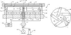
- the wafer holder and temperature conditioning arrangement 1also called chuck arrangement 1 , comprises a base arrangement 3 to be mounted to the wall 5 of a vacuum processing chamber with processing space P.
- the base arrangement 3has, pointing towards the processing space P, with a pattern of protruding ribs 7 concentric about a central axis A of the overall chuck arrangement 1 .
- Within the base arrangements 3there is provided, again concentrically to axis A, a heater compartment 9 as a ring shaped chamber wherein four heater lamp tubes 11 are mounted and operated.
- the heater lamp tubes 11are each distinctly located in the heater compartment 9 with different spacing's from axis A and with different angular orientations with respect to radial direction r from axis A to the circular periphery-wall of the heater compartment 9 .
- the heater compartment 9 and thus the heater lamp tubes 11are in vacuum within the processing chamber.
- the concentric pattern of protruding ribs 7match with a pattern of respective circular grooves 13 worked one surface of a metal, circular wafer carrier plate 15 .
- the effective surface for heat transfer between the base arrangement 3 and the metal, circular wafer carrier plate 15is doubled.
- the base arrangement 3 as well as the metal, circular wafer carrier plate 15is coated with a special black coating that absorbs heat radiation i.e. infrared radiation.
- the metal, circular wafer carrier plate 15is driven by means of a driver shaft 17 operationally connected to a servo motor 19 .
- the driver shaft 17 , coaxial to axis A, and the metal, circular wafer carrier plate 15are electrically isolated from base arrangement 3 and from the wall 5 of the vacuum processing chamber and may thus (not shown) be operated at any desired electrical bias signal.
- the driver shaft 17further comprises a coaxial gas feed line 21 , which, on one hand, is operationally connected to a gas source arrangement 23 and which abuts, on the other hand, in a gas outlet and gas diverting system 26 with gas distribution grooves 28 provided in the substantially plane surface 25 of the metal, circular wafer carrier plate 15 whereupon a wafer 27 to be processed is located in operation.
- the wafer 27is retained upon the metal, circular wafer carrier plate 15 by means of a weight ring 29 which, by its proper weight, biases the wafer 27 towards and upon the addressed surface 25 of the metal, circular wafer carrier plate 15 .
- the base arrangement 3further comprises a piping of a cooling system 31 conceived to flow a liquid cooling medium in the base arrangement 3 .
- Heat transfer from or to the wafer 27 from the heater compartment 9 or from the cooling system 31 with pipingis performed over a solid material surface interface between base arrangement 3 to the metal circular wafer carrier plate 15 and from that plate 15 over of the back gas cushion to or from wafer 27 .
- thermical inertia especially of the base arrangement 3do substantially contribute to the reaction time by which the temperature of wafer 27 reacts upon a heating or cooling step applied to the base arrangement 3 .
- two or four of the heater lamp tube 11are enabled.
- the individual location of the heater lamp tube 11 within the heater compartment 9is optimized to result, once thermal stability of the wafer 27 is reached in a homogenous temperature distribution along the wafer 27 , which is rotated as shown in FIG. 1 by w, together with the metal, circular wafer carrier plate 15 and the weight-ring 29 .
- 300 mm or 200 mm silicon wafersmay be processed.
- the maximum temperature that can be reached for the wafersis approximately 200° C. and thus the surface of metal, circular wafer carrier plate 15 may reach as well temperatures of approximately 200° C.
- the metal circular wafer carrier plateitself forms one wall of the heater compartment, wherein the heater lamp tubes are provided, the metal circular wafer carrier plate is directly heated by the heater lamp tubes by radiation and very small thermal inertia exist between a wafer applied to the addressed wafer carrier plate and the heater lamp tubes.
- this arrangementcomprises an electric power control unit, controlling power to the multitude of heater lamp tubes.
- This power control unitis conceived to operate the multitude of heater lamp tubes so as to establish along the other surface of the metal circular wafer carrier plate, opposite said one surface thereof, and thus whereupon in operation, the wafer resides, a maximum temperature of at least 800° C. averaged over the addressed other surface.
- the wafer carrier plateis in a today's preferred embodiment drivingly rotatable about the geometric axis in that, as was shown in context with FIG. 1 , a driver shaft is led through the base arrangement and coupled to the metal circular wafer carrier plate, which latter in today's preferred embodiment, is electrically isolated from the base arrangement to be operable at a desired electric bias potential.
- the wafer retaining arrangement of today's preferred embodimentis realised as was shown in FIG. 1 also by means of a weight ring but could also be realised in a different manner as e.g. by permanent magnet and/or electro magnetic retaining members.
- the multitude of heater lamp tubesconsist of a multitude of equal heater lamp tubes, which are mounted in the heater compartment equally oriented with respect to radial direction from the centre to the circular rim surface.
- the length extent direction of the heater lamp tubeis angularly offset with respect to the radial direction from the centre of the essentially plane surface towards the protruding circular rim surface.
- the position of at least a part of the heater lamp tubes in the heater compartmentmay be adjusted so as to optimize temperature distribution along a wafer disposed on the metal circular wafer carrier plate and rotated therewith and thus with respect to the heater lamp tubes.
- a gas outlet and dispensing arrangementthrough and along the other surface of the metal circular wafer carrier plate, which is that surface which is directly exposed to the wafer.
- the wafer retaining arrangementis a weight-ring dimensioned so as to reside on the periphery of a wafer to be processed, whereby the weight-ring is preferably conceived to be electrically connected to an electric bias source.
- the heater lamp tubeshave a thickness extent which fills the heater compartment between the extended essentially plane surface and the one surface of the metal circular wafer carrier plate without contacting these surfaces.
- the heater compartment thicknessis practically filled by the thickness extent of the heater lamp tubes.
- the extended essentially plane surface and the protruding peripherals circular rim surfaceare heat reflector surfaces, which are preferably high gloss polished.
- the metal circular wafer carrier plateis electrically isolated from the base arrangement and is preferably conceived to be electrically connected to an electric biasing source.
- the wafer carrier plateis conceived for one of
- the inventionis further directed on a method of manufacturing a wafer coated with a layer, comprising
- a wafer holder and temperature conditioning arrangementin any of the embodiments as addressed in context with such wafer holder and temperature conditioning arrangement according to the invention above may be applied. Further, if we talk about coating a “wafer”, we understand applying a coating upon such wafer, which includes that between the silicon wafer and the coating to be applied one or more than one layer have already been applied.
- the layer as appliedis of lead-zirconatetitanate, which is applied preferably by cosputtering lead, zirconium and titanium.
- FIG. 1A simplified and schematic view of a prior art rotating chuck arrangement.
- FIG. 2In a representation in analogy to that of FIG. 1 , a wafer holder and temperature conditioning arrangement according to the present invention, by which the method according to the present invention is realised.
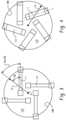
- FIG. 3A simplified and schematic top view on the heater compartment of a wafer holder and temperature conditioning arrangement according to the present invention and as exemplified in FIG. 2 for processing 100 mm diameter wafers.
- FIG. 4In a representation in analogy to that of FIG. 3 , the arrangement conceived to process 150 mm diameter wafers.
- a base arrangement 103is mounted to the wall 5 of a vacuum processing chamber with the processing span P.
- the base arrangement 103 of the wafer holder and temperature conditioning arrangement (chuck arrangement) 101 according to the present inventionhas a substantially planar surface 107 , which is bordered by a circular protruding rim surface 108 .
- the rim surface 108is circular about a central axis A of the substantially planar surface 107 of base arrangement 103 .
- the bin 109 thereby formed in the base arrangement 103is closed by a circular metal wafer carrier plate 115 , which is configured as already explained in context with FIG.
- a gas outlet—and distribution—system 128fed with a back gas through a gas feed line 121 centrally within driver shaft 117 for rotationally driving the metal circular wafer carrier plate 115 .
- a back gas cushionmay be applied between top surface of the metal circular wafer carrier plate 115 and a wafer 127 to be processed, as schematically shown from a gas reservoir 123 .
- the driver shaft 117is driven as schematically shown by motor 119 .
- vacuum seal 30 , 130 respectively,are provided.
- the bottom surface 116 of the metal circular wafer carrier plate 115closes the bin 109 , formed in the base arrangement 103 by the rim surface 108 and the substantially planar surface 107 , thereby defining for a heat compartment 110 :
- the heat compartment 110is limited on one side by the drivingly rotatable metal circular wafer carrier plate 115 .
- a multitude of heater lamp tubes 111are mounted, the metal circular wafer carrier plate being directly exposed to the heater lamp tubes 111 .
- the mount and electrical connections to the heater lamp tubes 111are only schematically shown in FIG. 2 at 111 o and 111 i .
- the surfaces of the bin 109namely protruding circular rim surface 108 as well as substantially planar surface 107 are realised as heat reflecting surfaces, are preferably high gloss polished.
- the heater lamp tubes 111are all equally oriented with respect to radial direction R from the centre A of the planar surface 107 to the circular rim surface 108 .
- four equal heater lamp tubes 111 with a nominal electric power of 500 W, halogen tubesare provided in the heater compartment 110 .
- the length axes ⁇ of the heater lamp tubes 111are equally angularly offset by an angle ⁇ from the radial direction R.
- the arrangement according to the inventionis conceived for a 150 mm diameter wafer.
- Five 500 W halogen heater lamp tubes 111are provided in the heater compartment 110 , the length axes ⁇ of which being again equally angularly offset with respect to any radial direction R.
- an arrangement according to the invention conceived for 200 mm diameter waferscomprises ten heater lamp tubes of 250 W nominal electric power.
- a power controller unit 134by which the electric power delivered to the heater lamp tubes 111 is controlled to provide at the surface of the metal circular wafer carrier plate 115 exposed to wafer 127 a maximum temperature of at least 800° C.
- the exact angular position of the length axes> of the heater lamp tubes 111may be adjusted as shown by ⁇ to optimize homogeneity of heat transfer to the revolving backside of the metal circular wafer carrier plate 115 .
- a piping of piping 131 for circulating a cooling liquid medium within the base arrangement 103there is provided in the base arrangement 103 , as already addressed for the known arrangement according to FIG. 1 , a piping of piping 131 for circulating a cooling liquid medium within the base arrangement 103 .
- the depth of the bin, formed by rim surface 108 and substantially planar surface 107substantially accords with the thickness extent of the tubes 111 , so that the tubes 111 considered in direction of axis A, fill the heater compartment 110 without contacting on one hand surfaces 108 / 107 and on the other hand the back surface 116 of metal circular wafer carrier plate 115 .
- the addressed plate 115is electrically isolated from base arrangement 103 and the processing chamber with the wall 5 so that (not shown) the wafer carrier plate 115 and thus the wafer carried thereon, may be operated at any desired biasing electric signal.
- the retaining arrangement for the wafer 127 upon the metal circular wafer carrier plate 115is realised by weight-ring 129 in analogy to the arrangement of FIG. 1 . It is also possible to provide the addressed weight-ring 129 with electrical contact, to apply to the wafer 127 via the addressed weight-ring 129 a desired electrical biasing signal (not shown).
- PZTlead-zirconatetitanate
Landscapes
- Engineering & Computer Science (AREA)
- Manufacturing & Machinery (AREA)
- Physics & Mathematics (AREA)
- Toxicology (AREA)
- Condensed Matter Physics & Semiconductors (AREA)
- General Physics & Mathematics (AREA)
- Health & Medical Sciences (AREA)
- Computer Hardware Design (AREA)
- Microelectronics & Electronic Packaging (AREA)
- Power Engineering (AREA)
- Container, Conveyance, Adherence, Positioning, Of Wafer (AREA)
- Physical Vapour Deposition (AREA)
- Chemical Vapour Deposition (AREA)
Abstract
Description
- a base arrangement with an extended, essentially plane surface, bordered by a protruding circular rim surface about the centre of the essentially plane surface;
- a metal circular wafer carrier plate mounted centred with respect to the centre of the essentially plane surface, one surface of the metal circular wafer carrier plate, the extended, essentially plane surface and the protruding circular rim surface, commonly defining a heater compartment, the metal wafer carrier plate being drivingly rotatable about a geometric axis through the centre of the essentially plane surface with respect to the base arrangement;
- a multitude of heater lamp tubes arranged in the heater compartment along the extended essentially plane surface and along the one surface of the metal circular wafer carrier plate and directly exposed to this surface and mounted to the base arrangement;
- a wafer retaining arrangement operationally coupled to the metal circular wafer carrier plate.
- a 100 mm diameter wafer, whereby the multitude of heater lamp tubes consists of four 500 W halogen heater lamp tubes;
- a 150 mm diameter wafer, whereby the addressed multitude consists of five 500 W halogen heater lamp tubes;
- a 200 mm diameter wafer, whereby the multitude as addressed, consists of ten 250 W halogen heater lamp tubes.
- providing in a vacuum process coating chamber a wafer holder and temperature conditioning arrangement, comprising:
- a base arrangement with an extended essentially plane surface, bordered by a protruding circular rim surface about the centre of the essentially plane surface;
- a metal circular wafer carrier plate centrally mounted with respect to the centre of the essentially plane surface, one surface of the metal circular wafer carrier plate, the extended, essentially plane surface and the protruding circular rim surface commonly defining a heater compartment, the metal circular wafer carrier plate being drivingly rotatable about a geometric axis through the centre of the essentially plane surface with respect to the base arrangement;
- a multitude of heater lamp tubes arranged in the heater compartment along the extended essentially plane surface and the one surface of the metal circular wafer carrier plate and directly exposed to the one surface of the metal circular wafer carrier plate and mounted to the base arrangement;
- a wafer retaining arrangement operationally coupled to the metal circular wafer carrier plate;
- an electric power control unit, controlling power to the multitude of heater lamp tubes and conceived to operate the multitude of heater lamp tubes so as to establish along the other surface of the metal circular wafer carrier plate, opposite the one surface thereof, a predetermined temperature, averaged over the other surface and,
- depositing on the other surface of the metal circular wafer carrier plate, a wafer to be coated;
- drivingly rotating the metal circular wafer carrier plate, while operating the electric power control unit to heat up the wafer to at least 800° C. and;
- depositing a layer on the wafer.
- providing in a vacuum process coating chamber a wafer holder and temperature conditioning arrangement, comprising:
Claims (25)
Priority Applications (1)
| Application Number | Priority Date | Filing Date | Title |
|---|---|---|---|
| US15/723,266US12249523B2 (en) | 2011-08-30 | 2017-10-03 | Wafer holder and temperature conditioning arrangement and method of manufacturing a wafer |
Applications Claiming Priority (2)
| Application Number | Priority Date | Filing Date | Title |
|---|---|---|---|
| US13/220,903US9793144B2 (en) | 2011-08-30 | 2011-08-30 | Wafer holder and temperature conditioning arrangement and method of manufacturing a wafer |
| US15/723,266US12249523B2 (en) | 2011-08-30 | 2017-10-03 | Wafer holder and temperature conditioning arrangement and method of manufacturing a wafer |
Related Parent Applications (1)
| Application Number | Title | Priority Date | Filing Date |
|---|---|---|---|
| US13/220,903DivisionUS9793144B2 (en) | 2011-08-30 | 2011-08-30 | Wafer holder and temperature conditioning arrangement and method of manufacturing a wafer |
Publications (2)
| Publication Number | Publication Date |
|---|---|
| US20180025925A1 US20180025925A1 (en) | 2018-01-25 |
| US12249523B2true US12249523B2 (en) | 2025-03-11 |
Family
ID=46851950
Family Applications (2)
| Application Number | Title | Priority Date | Filing Date |
|---|---|---|---|
| US13/220,903Active2033-07-24US9793144B2 (en) | 2011-08-30 | 2011-08-30 | Wafer holder and temperature conditioning arrangement and method of manufacturing a wafer |
| US15/723,266Active2033-05-27US12249523B2 (en) | 2011-08-30 | 2017-10-03 | Wafer holder and temperature conditioning arrangement and method of manufacturing a wafer |
Family Applications Before (1)
| Application Number | Title | Priority Date | Filing Date |
|---|---|---|---|
| US13/220,903Active2033-07-24US9793144B2 (en) | 2011-08-30 | 2011-08-30 | Wafer holder and temperature conditioning arrangement and method of manufacturing a wafer |
Country Status (5)
| Country | Link |
|---|---|
| US (2) | US9793144B2 (en) |
| EP (1) | EP2751833B1 (en) |
| KR (1) | KR101985039B1 (en) |
| CN (2) | CN103814434B (en) |
| WO (1) | WO2013030190A1 (en) |
Families Citing this family (12)
| Publication number | Priority date | Publication date | Assignee | Title |
|---|---|---|---|---|
| CN103123906A (en)* | 2011-11-18 | 2013-05-29 | 中芯国际集成电路制造(北京)有限公司 | Reaction device for processing wafer, electrostatic chuck and wafer temperature control method |
| GB201305674D0 (en)* | 2013-03-28 | 2013-05-15 | Spts Technologies Ltd | Method and apparatus for processing a semiconductor workpiece |
| US9853579B2 (en)* | 2013-12-18 | 2017-12-26 | Applied Materials, Inc. | Rotatable heated electrostatic chuck |
| TW201639063A (en)* | 2015-01-22 | 2016-11-01 | 應用材料股份有限公司 | Batch heating and cooling chamber or loadlock |
| US9633886B2 (en)* | 2015-04-16 | 2017-04-25 | Varian Semiconductor Equipment Associates, Inc. | Hybrid thermal electrostatic clamp |
| US9685303B2 (en) | 2015-05-08 | 2017-06-20 | Varian Semiconductor Equipment Associates, Inc. | Apparatus for heating and processing a substrate |
| US9728430B2 (en)* | 2015-06-29 | 2017-08-08 | Varian Semiconductor Equipment Associates, Inc. | Electrostatic chuck with LED heating |
| CN105714380A (en)* | 2016-04-26 | 2016-06-29 | 北京世纪金光半导体有限公司 | Silicon carbide epitaxial growth device and method |
| JP6215426B1 (en)* | 2016-09-21 | 2017-10-18 | オリジン電気株式会社 | Heating device and method for manufacturing plate-like member |
| CN110299314A (en)* | 2019-07-04 | 2019-10-01 | 北京北方华创微电子装备有限公司 | Heating system and semiconductor processing equipment |
| US12046503B2 (en)* | 2021-10-26 | 2024-07-23 | Applied Materials, Inc. | Chuck for processing semiconductor workpieces at high temperatures |
| WO2025002740A1 (en) | 2023-06-30 | 2025-01-02 | Evatec Ag | Wafer holder |
Citations (32)
| Publication number | Priority date | Publication date | Assignee | Title |
|---|---|---|---|---|
| US3836751A (en)* | 1973-07-26 | 1974-09-17 | Applied Materials Inc | Temperature controlled profiling heater |
| US4823735A (en)* | 1987-05-12 | 1989-04-25 | Gemini Research, Inc. | Reflector apparatus for chemical vapor deposition reactors |
| US4845055A (en)* | 1987-05-21 | 1989-07-04 | Yamaha Corporation | Rapid annealing under high pressure for use in fabrication of semiconductor device |
| US5228501A (en) | 1986-12-19 | 1993-07-20 | Applied Materials, Inc. | Physical vapor deposition clamping mechanism and heater/cooler |
| US6007635A (en)* | 1997-11-26 | 1999-12-28 | Micro C Technologies, Inc. | Platform for supporting a semiconductor substrate and method of supporting a substrate during rapid high temperature processing |
| US6022413A (en)* | 1995-06-16 | 2000-02-08 | Ebara Corporation | Thin-film vapor deposition apparatus |
| US6210539B1 (en)* | 1997-05-14 | 2001-04-03 | Applied Materials, Inc. | Method and apparatus for producing a uniform density plasma above a substrate |
| US6310323B1 (en)* | 2000-03-24 | 2001-10-30 | Micro C Technologies, Inc. | Water cooled support for lamps and rapid thermal processing chamber |
| US20020106826A1 (en)* | 2001-02-07 | 2002-08-08 | Vadim Boguslavskiy | Susceptorless reactor for growing epitaxial layers on wafers by chemical vapor deposition |
| US20020139307A1 (en)* | 2000-12-04 | 2002-10-03 | Applied Materials, Inc. | Cooling gas delivery system for a rotatable semiconductor substrate support assembly |
| US20030070915A1 (en) | 2001-10-12 | 2003-04-17 | Taiwan Semiconductor Manufacturing Co., Ltd. | Apparatus and method for self-centering a wafer in a sputter chamber |
| US20030094446A1 (en) | 2001-04-17 | 2003-05-22 | Mattson Technology, Inc. | Rapid thermal processing system for integrated circuits |
| US6645344B2 (en) | 2001-05-18 | 2003-11-11 | Tokyo Electron Limited | Universal backplane assembly and methods |
| US6658895B2 (en)* | 2001-08-16 | 2003-12-09 | Richter Precision, Inc. | Carbon nitride coating for optical media discs |
| US20040011286A1 (en)* | 2002-07-19 | 2004-01-22 | Hynix Semiconductor Inc. | Batch type atomic layer deposition apparatus and in-situ cleaning method thereof |
| US20050053369A1 (en)* | 2003-09-08 | 2005-03-10 | Wafermasters, Inc. | Focused photon energy heating chamber |
| US20060249695A1 (en) | 2005-05-04 | 2006-11-09 | Hoon Choi | Heat reflector and substrate processing apparatus comprising the same |
| US20070017445A1 (en)* | 2005-07-19 | 2007-01-25 | Takako Takehara | Hybrid PVD-CVD system |
| US20070028838A1 (en)* | 2005-07-29 | 2007-02-08 | Craig Bercaw | Gas manifold valve cluster |
| US20080108171A1 (en)* | 2006-09-20 | 2008-05-08 | Rogers John A | Release strategies for making transferable semiconductor structures, devices and device components |
| US7396746B2 (en) | 2004-05-24 | 2008-07-08 | Varian Semiconductor Equipment Associates, Inc. | Methods for stable and repeatable ion implantation |
| US20080276860A1 (en) | 2007-05-10 | 2008-11-13 | Burrows Brian H | Cross flow apparatus and method for hydride vapor phase deposition |
| US20090101633A1 (en)* | 2007-10-19 | 2009-04-23 | Asm America, Inc. | Reactor with small linear lamps for localized heat control and improved temperature uniformity |
| US20090179365A1 (en) | 2008-01-15 | 2009-07-16 | Lerner Alexander N | High temperature vacuum chuck assembly |
| US20090269490A1 (en)* | 2008-04-25 | 2009-10-29 | Yoshikazu Moriyama | Coating apparatus and coating method |
| US20090311430A1 (en)* | 2008-06-16 | 2009-12-17 | Hideki Ito | Coating apparatus and coating method |
| US20100111511A1 (en) | 2008-10-31 | 2010-05-06 | Nir Merry | Use of infrared camera for real-time temperature monitoring and control |
| US20100304027A1 (en)* | 2009-05-27 | 2010-12-02 | Applied Materials, Inc. | Substrate processing system and methods thereof |
| US20110143019A1 (en)* | 2009-12-14 | 2011-06-16 | Amprius, Inc. | Apparatus for Deposition on Two Sides of the Web |
| US20110244128A1 (en)* | 2010-03-31 | 2011-10-06 | Tokyo Electron Limited | Flow plate utilization in filament assisted chemical vapor deposition |
| US20120037068A1 (en)* | 2010-08-11 | 2012-02-16 | Applied Materials, Inc. | Composite substrates for direct heating and increased temperature uniformity |
| US20120193337A1 (en)* | 2011-02-02 | 2012-08-02 | Bsh Home Appliances Corporation | Electric oven with a heating element reflector |
Family Cites Families (4)
| Publication number | Priority date | Publication date | Assignee | Title |
|---|---|---|---|---|
| JPH0323629A (en)* | 1989-06-21 | 1991-01-31 | Nec Corp | Manufacture apparatus for semiconductor element |
| JPH10339591A (en)* | 1997-06-10 | 1998-12-22 | Komatsu Ltd | Temperature controller utilizing heat pipe |
| JP4675579B2 (en)* | 2003-06-30 | 2011-04-27 | 大日本スクリーン製造株式会社 | Optical energy absorption ratio measuring method, optical energy absorption ratio measuring apparatus and heat treatment apparatus |
| US8135560B2 (en)* | 2009-01-30 | 2012-03-13 | Applied Materials, Inc. | Sensor system for semiconductor manufacturing apparatus |
- 2011
- 2011-08-30USUS13/220,903patent/US9793144B2/enactiveActive
- 2012
- 2012-08-28WOPCT/EP2012/066679patent/WO2013030190A1/enunknown
- 2012-08-28EPEP12759391.1Apatent/EP2751833B1/enactiveActive
- 2012-08-28CNCN201280042393.1Apatent/CN103814434B/enactiveActive
- 2012-08-28CNCN201710507447.1Apatent/CN107452655B/enactiveActive
- 2012-08-28KRKR1020147006779Apatent/KR101985039B1/enactiveActive
- 2017
- 2017-10-03USUS15/723,266patent/US12249523B2/enactiveActive
Patent Citations (32)
| Publication number | Priority date | Publication date | Assignee | Title |
|---|---|---|---|---|
| US3836751A (en)* | 1973-07-26 | 1974-09-17 | Applied Materials Inc | Temperature controlled profiling heater |
| US5228501A (en) | 1986-12-19 | 1993-07-20 | Applied Materials, Inc. | Physical vapor deposition clamping mechanism and heater/cooler |
| US4823735A (en)* | 1987-05-12 | 1989-04-25 | Gemini Research, Inc. | Reflector apparatus for chemical vapor deposition reactors |
| US4845055A (en)* | 1987-05-21 | 1989-07-04 | Yamaha Corporation | Rapid annealing under high pressure for use in fabrication of semiconductor device |
| US6022413A (en)* | 1995-06-16 | 2000-02-08 | Ebara Corporation | Thin-film vapor deposition apparatus |
| US6210539B1 (en)* | 1997-05-14 | 2001-04-03 | Applied Materials, Inc. | Method and apparatus for producing a uniform density plasma above a substrate |
| US6007635A (en)* | 1997-11-26 | 1999-12-28 | Micro C Technologies, Inc. | Platform for supporting a semiconductor substrate and method of supporting a substrate during rapid high temperature processing |
| US6310323B1 (en)* | 2000-03-24 | 2001-10-30 | Micro C Technologies, Inc. | Water cooled support for lamps and rapid thermal processing chamber |
| US20020139307A1 (en)* | 2000-12-04 | 2002-10-03 | Applied Materials, Inc. | Cooling gas delivery system for a rotatable semiconductor substrate support assembly |
| US20020106826A1 (en)* | 2001-02-07 | 2002-08-08 | Vadim Boguslavskiy | Susceptorless reactor for growing epitaxial layers on wafers by chemical vapor deposition |
| US20030094446A1 (en) | 2001-04-17 | 2003-05-22 | Mattson Technology, Inc. | Rapid thermal processing system for integrated circuits |
| US6645344B2 (en) | 2001-05-18 | 2003-11-11 | Tokyo Electron Limited | Universal backplane assembly and methods |
| US6658895B2 (en)* | 2001-08-16 | 2003-12-09 | Richter Precision, Inc. | Carbon nitride coating for optical media discs |
| US20030070915A1 (en) | 2001-10-12 | 2003-04-17 | Taiwan Semiconductor Manufacturing Co., Ltd. | Apparatus and method for self-centering a wafer in a sputter chamber |
| US20040011286A1 (en)* | 2002-07-19 | 2004-01-22 | Hynix Semiconductor Inc. | Batch type atomic layer deposition apparatus and in-situ cleaning method thereof |
| US20050053369A1 (en)* | 2003-09-08 | 2005-03-10 | Wafermasters, Inc. | Focused photon energy heating chamber |
| US7396746B2 (en) | 2004-05-24 | 2008-07-08 | Varian Semiconductor Equipment Associates, Inc. | Methods for stable and repeatable ion implantation |
| US20060249695A1 (en) | 2005-05-04 | 2006-11-09 | Hoon Choi | Heat reflector and substrate processing apparatus comprising the same |
| US20070017445A1 (en)* | 2005-07-19 | 2007-01-25 | Takako Takehara | Hybrid PVD-CVD system |
| US20070028838A1 (en)* | 2005-07-29 | 2007-02-08 | Craig Bercaw | Gas manifold valve cluster |
| US20080108171A1 (en)* | 2006-09-20 | 2008-05-08 | Rogers John A | Release strategies for making transferable semiconductor structures, devices and device components |
| US20080276860A1 (en) | 2007-05-10 | 2008-11-13 | Burrows Brian H | Cross flow apparatus and method for hydride vapor phase deposition |
| US20090101633A1 (en)* | 2007-10-19 | 2009-04-23 | Asm America, Inc. | Reactor with small linear lamps for localized heat control and improved temperature uniformity |
| US20090179365A1 (en) | 2008-01-15 | 2009-07-16 | Lerner Alexander N | High temperature vacuum chuck assembly |
| US20090269490A1 (en)* | 2008-04-25 | 2009-10-29 | Yoshikazu Moriyama | Coating apparatus and coating method |
| US20090311430A1 (en)* | 2008-06-16 | 2009-12-17 | Hideki Ito | Coating apparatus and coating method |
| US20100111511A1 (en) | 2008-10-31 | 2010-05-06 | Nir Merry | Use of infrared camera for real-time temperature monitoring and control |
| US20100304027A1 (en)* | 2009-05-27 | 2010-12-02 | Applied Materials, Inc. | Substrate processing system and methods thereof |
| US20110143019A1 (en)* | 2009-12-14 | 2011-06-16 | Amprius, Inc. | Apparatus for Deposition on Two Sides of the Web |
| US20110244128A1 (en)* | 2010-03-31 | 2011-10-06 | Tokyo Electron Limited | Flow plate utilization in filament assisted chemical vapor deposition |
| US20120037068A1 (en)* | 2010-08-11 | 2012-02-16 | Applied Materials, Inc. | Composite substrates for direct heating and increased temperature uniformity |
| US20120193337A1 (en)* | 2011-02-02 | 2012-08-02 | Bsh Home Appliances Corporation | Electric oven with a heating element reflector |
Also Published As
| Publication number | Publication date |
|---|---|
| WO2013030190A1 (en) | 2013-03-07 |
| EP2751833B1 (en) | 2021-07-21 |
| US20130052834A1 (en) | 2013-02-28 |
| US20180025925A1 (en) | 2018-01-25 |
| CN103814434B (en) | 2017-08-08 |
| EP2751833A1 (en) | 2014-07-09 |
| KR101985039B1 (en) | 2019-05-31 |
| CN107452655B (en) | 2021-03-12 |
| US9793144B2 (en) | 2017-10-17 |
| KR20140068969A (en) | 2014-06-09 |
| CN103814434A (en) | 2014-05-21 |
| CN107452655A (en) | 2017-12-08 |
Similar Documents
| Publication | Publication Date | Title |
|---|---|---|
| US12249523B2 (en) | Wafer holder and temperature conditioning arrangement and method of manufacturing a wafer | |
| US20130118407A1 (en) | Substrate susceptor and deposition apparatus having same | |
| US7901552B2 (en) | Sputtering target with grooves and intersecting channels | |
| KR100313309B1 (en) | Method of implementing temperature controlled process and processing device for semiconductor wafer | |
| TWI755461B (en) | Rotatable electrostatic chuck having backside gas supply | |
| US10978276B2 (en) | Substrate processing apparatus including top reflector above annular lamp assembly | |
| US8475596B2 (en) | Apparatus to process coating material using flame nozzle and evaporation deposition device having same | |
| KR20160042570A (en) | Physical vapor deposition apparatus and method of depositing phase-change materials using the same | |
| CN112680707B (en) | Workpiece carrier, thin film deposition chamber, thin film deposition method | |
| KR100375396B1 (en) | Reaction chamber with semi-high temperature wall | |
| JP6997863B2 (en) | Vacuum processing equipment | |
| TWI802617B (en) | Substrate processing apparatus and method of processing a substrate and of manufacturing a processed workpiece | |
| JP7354090B2 (en) | Cathode assembly with dual position magnetron and centrally delivered coolant | |
| JP7078752B2 (en) | Vacuum processing equipment | |
| JPH09237763A (en) | Single wafer processing heat treatment apparatus | |
| JP2009275255A (en) | Vapor phase growth apparatus | |
| JP2000260720A (en) | Semiconductor manufacturing equipment | |
| JPH0997765A (en) | Substrate processing equipment | |
| US9953829B2 (en) | Image processing apparatus with improved slide printout based on layout data | |
| JPH05144406A (en) | Processing device | |
| EP0330708B1 (en) | Apparatus for forming thin films | |
| JPH0689892A (en) | Plasma cvd device |
Legal Events
| Date | Code | Title | Description |
|---|---|---|---|
| FEPP | Fee payment procedure | Free format text:ENTITY STATUS SET TO UNDISCOUNTED (ORIGINAL EVENT CODE: BIG.); ENTITY STATUS OF PATENT OWNER: LARGE ENTITY | |
| STPP | Information on status: patent application and granting procedure in general | Free format text:DOCKETED NEW CASE - READY FOR EXAMINATION | |
| STPP | Information on status: patent application and granting procedure in general | Free format text:NON FINAL ACTION MAILED | |
| STPP | Information on status: patent application and granting procedure in general | Free format text:RESPONSE TO NON-FINAL OFFICE ACTION ENTERED AND FORWARDED TO EXAMINER | |
| STPP | Information on status: patent application and granting procedure in general | Free format text:RESPONSE AFTER FINAL ACTION FORWARDED TO EXAMINER | |
| STPP | Information on status: patent application and granting procedure in general | Free format text:NON FINAL ACTION MAILED | |
| STPP | Information on status: patent application and granting procedure in general | Free format text:RESPONSE TO NON-FINAL OFFICE ACTION ENTERED AND FORWARDED TO EXAMINER | |
| STPP | Information on status: patent application and granting procedure in general | Free format text:FINAL REJECTION MAILED | |
| STPP | Information on status: patent application and granting procedure in general | Free format text:DOCKETED NEW CASE - READY FOR EXAMINATION | |
| STPP | Information on status: patent application and granting procedure in general | Free format text:NON FINAL ACTION MAILED | |
| STPP | Information on status: patent application and granting procedure in general | Free format text:RESPONSE TO NON-FINAL OFFICE ACTION ENTERED AND FORWARDED TO EXAMINER | |
| STPP | Information on status: patent application and granting procedure in general | Free format text:FINAL REJECTION MAILED | |
| STPP | Information on status: patent application and granting procedure in general | Free format text:ADVISORY ACTION MAILED | |
| STPP | Information on status: patent application and granting procedure in general | Free format text:DOCKETED NEW CASE - READY FOR EXAMINATION | |
| STPP | Information on status: patent application and granting procedure in general | Free format text:NON FINAL ACTION MAILED | |
| STPP | Information on status: patent application and granting procedure in general | Free format text:RESPONSE TO NON-FINAL OFFICE ACTION ENTERED AND FORWARDED TO EXAMINER | |
| STPP | Information on status: patent application and granting procedure in general | Free format text:NOTICE OF ALLOWANCE MAILED -- APPLICATION RECEIVED IN OFFICE OF PUBLICATIONS | |
| STPP | Information on status: patent application and granting procedure in general | Free format text:PUBLICATIONS -- ISSUE FEE PAYMENT VERIFIED | |
| STCF | Information on status: patent grant | Free format text:PATENTED CASE |