US12240748B2 - MEMS die and MEMS-based sensor - Google Patents
MEMS die and MEMS-based sensorDownload PDFInfo
- Publication number
- US12240748B2 US12240748B2US17/207,722US202117207722AUS12240748B2US 12240748 B2US12240748 B2US 12240748B2US 202117207722 AUS202117207722 AUS 202117207722AUS 12240748 B2US12240748 B2US 12240748B2
- Authority
- US
- United States
- Prior art keywords
- diaphragm
- electrode
- mems die
- mems
- piston
- Prior art date
- Legal status (The legal status is an assumption and is not a legal conclusion. Google has not performed a legal analysis and makes no representation as to the accuracy of the status listed.)
- Active, expires
Links
Images


Classifications
- B—PERFORMING OPERATIONS; TRANSPORTING
- B81—MICROSTRUCTURAL TECHNOLOGY
- B81B—MICROSTRUCTURAL DEVICES OR SYSTEMS, e.g. MICROMECHANICAL DEVICES
- B81B3/00—Devices comprising flexible or deformable elements, e.g. comprising elastic tongues or membranes
- B81B3/0018—Structures acting upon the moving or flexible element for transforming energy into mechanical movement or vice versa, i.e. actuators, sensors, generators
- B81B3/0021—Transducers for transforming electrical into mechanical energy or vice versa
- H—ELECTRICITY
- H04—ELECTRIC COMMUNICATION TECHNIQUE
- H04R—LOUDSPEAKERS, MICROPHONES, GRAMOPHONE PICK-UPS OR LIKE ACOUSTIC ELECTROMECHANICAL TRANSDUCERS; DEAF-AID SETS; PUBLIC ADDRESS SYSTEMS
- H04R1/00—Details of transducers, loudspeakers or microphones
- H04R1/02—Casings; Cabinets ; Supports therefor; Mountings therein
- H04R1/04—Structural association of microphone with electric circuitry therefor
- H—ELECTRICITY
- H04—ELECTRIC COMMUNICATION TECHNIQUE
- H04R—LOUDSPEAKERS, MICROPHONES, GRAMOPHONE PICK-UPS OR LIKE ACOUSTIC ELECTROMECHANICAL TRANSDUCERS; DEAF-AID SETS; PUBLIC ADDRESS SYSTEMS
- H04R19/00—Electrostatic transducers
- B—PERFORMING OPERATIONS; TRANSPORTING
- B81—MICROSTRUCTURAL TECHNOLOGY
- B81B—MICROSTRUCTURAL DEVICES OR SYSTEMS, e.g. MICROMECHANICAL DEVICES
- B81B3/00—Devices comprising flexible or deformable elements, e.g. comprising elastic tongues or membranes
- B81B3/0035—Constitution or structural means for controlling the movement of the flexible or deformable elements
- B81B3/0054—For holding or placing an element in a given position
- H—ELECTRICITY
- H04—ELECTRIC COMMUNICATION TECHNIQUE
- H04R—LOUDSPEAKERS, MICROPHONES, GRAMOPHONE PICK-UPS OR LIKE ACOUSTIC ELECTROMECHANICAL TRANSDUCERS; DEAF-AID SETS; PUBLIC ADDRESS SYSTEMS
- H04R17/00—Piezoelectric transducers; Electrostrictive transducers
- H04R17/02—Microphones
- H—ELECTRICITY
- H04—ELECTRIC COMMUNICATION TECHNIQUE
- H04R—LOUDSPEAKERS, MICROPHONES, GRAMOPHONE PICK-UPS OR LIKE ACOUSTIC ELECTROMECHANICAL TRANSDUCERS; DEAF-AID SETS; PUBLIC ADDRESS SYSTEMS
- H04R19/00—Electrostatic transducers
- H04R19/005—Electrostatic transducers using semiconductor materials
- H—ELECTRICITY
- H04—ELECTRIC COMMUNICATION TECHNIQUE
- H04R—LOUDSPEAKERS, MICROPHONES, GRAMOPHONE PICK-UPS OR LIKE ACOUSTIC ELECTROMECHANICAL TRANSDUCERS; DEAF-AID SETS; PUBLIC ADDRESS SYSTEMS
- H04R7/00—Diaphragms for electromechanical transducers; Cones
- H04R7/02—Diaphragms for electromechanical transducers; Cones characterised by the construction
- H04R7/04—Plane diaphragms
- H04R7/06—Plane diaphragms comprising a plurality of sections or layers
- H04R7/08—Plane diaphragms comprising a plurality of sections or layers comprising superposed layers separated by air or other fluid
- B—PERFORMING OPERATIONS; TRANSPORTING
- B81—MICROSTRUCTURAL TECHNOLOGY
- B81B—MICROSTRUCTURAL DEVICES OR SYSTEMS, e.g. MICROMECHANICAL DEVICES
- B81B2201/00—Specific applications of microelectromechanical systems
- B81B2201/02—Sensors
- B81B2201/0257—Microphones or microspeakers
- B—PERFORMING OPERATIONS; TRANSPORTING
- B81—MICROSTRUCTURAL TECHNOLOGY
- B81B—MICROSTRUCTURAL DEVICES OR SYSTEMS, e.g. MICROMECHANICAL DEVICES
- B81B2203/00—Basic microelectromechanical structures
- B81B2203/01—Suspended structures, i.e. structures allowing a movement
- B81B2203/0127—Diaphragms, i.e. structures separating two media that can control the passage from one medium to another; Membranes, i.e. diaphragms with filtering function
- B—PERFORMING OPERATIONS; TRANSPORTING
- B81—MICROSTRUCTURAL TECHNOLOGY
- B81B—MICROSTRUCTURAL DEVICES OR SYSTEMS, e.g. MICROMECHANICAL DEVICES
- B81B2203/00—Basic microelectromechanical structures
- B81B2203/04—Electrodes
- H—ELECTRICITY
- H04—ELECTRIC COMMUNICATION TECHNIQUE
- H04R—LOUDSPEAKERS, MICROPHONES, GRAMOPHONE PICK-UPS OR LIKE ACOUSTIC ELECTROMECHANICAL TRANSDUCERS; DEAF-AID SETS; PUBLIC ADDRESS SYSTEMS
- H04R1/00—Details of transducers, loudspeakers or microphones
- H04R1/02—Casings; Cabinets ; Supports therefor; Mountings therein
- H04R1/021—Casings; Cabinets ; Supports therefor; Mountings therein incorporating only one transducer
- H—ELECTRICITY
- H04—ELECTRIC COMMUNICATION TECHNIQUE
- H04R—LOUDSPEAKERS, MICROPHONES, GRAMOPHONE PICK-UPS OR LIKE ACOUSTIC ELECTROMECHANICAL TRANSDUCERS; DEAF-AID SETS; PUBLIC ADDRESS SYSTEMS
- H04R19/00—Electrostatic transducers
- H04R19/04—Microphones
- H—ELECTRICITY
- H04—ELECTRIC COMMUNICATION TECHNIQUE
- H04R—LOUDSPEAKERS, MICROPHONES, GRAMOPHONE PICK-UPS OR LIKE ACOUSTIC ELECTROMECHANICAL TRANSDUCERS; DEAF-AID SETS; PUBLIC ADDRESS SYSTEMS
- H04R2201/00—Details of transducers, loudspeakers or microphones covered by H04R1/00 but not provided for in any of its subgroups
- H04R2201/003—Mems transducers or their use
- H—ELECTRICITY
- H04—ELECTRIC COMMUNICATION TECHNIQUE
- H04R—LOUDSPEAKERS, MICROPHONES, GRAMOPHONE PICK-UPS OR LIKE ACOUSTIC ELECTROMECHANICAL TRANSDUCERS; DEAF-AID SETS; PUBLIC ADDRESS SYSTEMS
- H04R2207/00—Details of diaphragms or cones for electromechanical transducers or their suspension covered by H04R7/00 but not provided for in H04R7/00 or in H04R2307/00
- H04R2207/021—Diaphragm extensions, not necessarily integrally formed, e.g. skirts, rims, flanges
- H—ELECTRICITY
- H04—ELECTRIC COMMUNICATION TECHNIQUE
- H04R—LOUDSPEAKERS, MICROPHONES, GRAMOPHONE PICK-UPS OR LIKE ACOUSTIC ELECTROMECHANICAL TRANSDUCERS; DEAF-AID SETS; PUBLIC ADDRESS SYSTEMS
- H04R2410/00—Microphones
- H04R2410/03—Reduction of intrinsic noise in microphones
Definitions
- the present disclosurerelates to microelectromechanical systems (MEMS) dies and MEMS-based sensors.
- MEMSmicroelectromechanical systems
- Microphone assembliesthat include microelectromechanical systems (MEMS) dies convert acoustic energy into an electrical signal.
- the microphone assembliesmay be employed in mobile communication devices, laptop computers, and appliances, among other devices and machinery.
- An important parameter for a microphone assemblyis the acoustic signal-to-noise ratio (SNR), which compares the desired signal level (e.g., the signal amplitude due to acoustic disturbances captured by the microphone assembly) to the level of background noise.
- SNRacoustic signal-to-noise ratio
- SNRacoustic signal-to-noise ratio
- MEMS acoustic diesSNR often limits the smallest dimensions that can be achieved and the overall package size of the microphone assembly.
- FIG. 1is a side cross-sectional view of a MEMS microphone, according to an embodiment.
- FIG. 2is a signal lumped element model for the MEMS microphone of FIG. 1 , according to an embodiment.
- FIG. 3is a side cross-sectional view of a MEMS microphone that shows a thermal boundary layer within a back volume of the MEMS microphone, according to an embodiment.
- FIG. 4is a signal lumped element model for the MEMS microphone of FIG. 3 , according to an embodiment.
- FIG. 5is a side cross-sectional view of a MEMS die, according to an embodiment.
- FIG. 6is a partial reproduction of FIG. 5 , showing an area near a back volume for the MEMS die.
- FIG. 7is a side cross-sectional view of a MEMS die with piezoelectric elements, according to an embodiment.
- FIG. 8is a side cross-sectional view of a MEMS die with piezoelectric elements, according to another embodiment.
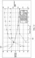
- FIG. 9is a graph of acoustic noise as a function of back volume for a MEMS die, according to an embodiment.
- FIG. 10is a graph showing the variation of thermal boundary layer thickness as a function of sound frequency.
- FIG. 11is a graph showing the acoustic damping as a function of frequency of both a conventional microphone assembly and a microphone assembly configured according to an embodiment of the disclosure as a function of gap height within a MEMS die.
- FIG. 12is a graph of acoustic SNR as a function of gap height within a MEMS die.
- FIG. 13is a graph of acoustic SNR and sensitivity as a function of gap height within a MEMS die.
- FIG. 14is a side cross-sectional view of a MEMS die, according to another embodiment.
- FIG. 15is a graph of acoustic SNR as a function of gap height within a MEMS die configured according to an embodiment over a range of different diaphragm pierce diameters for the MEMS die.
- FIG. 16is a perspective and sectional view of a MEMS die, according to another embodiment.
- FIG. 17is a side cross-sectional view of the MEMS die of FIG. 16 .
- FIG. 19is a side cross-sectional view of a MEMS die, according to another embodiment.
- FIG. 20is a side cross-sectional view of a MEMS die that is integrally formed onto an integrated circuit, according to an embodiment.
- FIG. 21is a side cross-sectional view of a microphone assembly, according to an embodiment.
- FIG. 22is a side cross-sectional view of a microphone assembly, according to another embodiment.
- FIG. 23is a side cross-sectional view of a microphone assembly, according to another embodiment.
- FIG. 24 Ais a side cross-sectional view of a MEMS die having a movable piston, according to an embodiment.
- FIG. 24 Bis a side cross-sectional view of a MEMS die that is a variation of the MEMS die of FIG. 24 A .
- FIG. 24 Cis a partial perspective cross-sectional view of a possible implementation of the electrode of FIG. 24 A .
- FIG. 24 Dis a top-down view of another possible implementation of the electrode of FIG. 24 A .
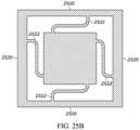
- FIG. 25 Ais a side cross-sectional view of a MEMS die having a movable piston, according to an embodiment.
- FIG. 25 Bis a top view of the piston, walls, and external conductors of a possible implementation of the MEMS die of FIG. 25 A .
- FIG. 25 Cis a side cross-sectional view of a MEMS die that is a variation of the MEMS die of FIG. 25 A .
- FIG. 25 Dis a side cross-sectional view of a MEMS die that is another variation of the MEMS die of FIG. 25 A .
- FIG. 25 Eis a partial perspective cross-sectional view of a possible implementation of the substrate of the MEMS die FIG. 25 A .
- FIG. 25 Fis a top-down cross-sectional view of another possible implementation of the substrate of the MEMS die of FIG. 25 A .
- FIG. 26 Ais a side cross-sectional view of a MEMS die having a movable piston, according to an embodiment.
- FIG. 26 Bis a partial perspective cross-sectional view of a possible implementation of the substrate of the piston of FIG. 26 A .
- FIG. 26 Cis a bottom-up view of a possible implementation of the piston of the MEMS die of FIG. 26 A .
- FIG. 26 Dis a side cross-sectional view of a MEMS die that is a variation of the MEMS die of FIG. 26 A .
- FIG. 26 Eis a side cross-sectional view of a MEMS die that is another variation of the MEMS die of FIG. 26 A .
- FIG. 26 Fis a side cross-sectional view of a MEMS die that is yet another variation of the MEMS die of FIG. 26 A , according to another embodiment.
- FIG. 27is a side cross-section view of a MEMS die that includes a dual-diaphragm assembly, according to an embodiment.
- FIG. 28 Ais a side cross-section view of a MEMS die that includes a dual-diaphragm assembly, according to another embodiment.
- FIG. 28 Bis a side cross-section view of a MEMS die that includes a single-diaphragm assembly but with the same enclosure and substrate as the MEMS die of FIG. 28 A , according to an embodiment.
- FIG. 28 Cis a side cross-sectional view of a variation of the MEMS die of FIG. 28 B .
- FIG. 29is a sensor that incorporates the MEMS die of FIG. 27 , according to an embodiment.
- FIG. 30is a sensor that incorporates the MEMS die of FIG. 28 A , according to an embodiment.
- FIG. 31 A and FIG. 31 Bdepict the operation of a dielectric motor MEMS device, according to an embodiment.
- FIG. 32depicts the operation of a dielectric motor MEMS device, according to another embodiment.
- FIG. 33is a perspective view of a dual-diaphragm, solid dielectric MEMS assembly, according to an embodiment.
- FIG. 34is a side cross-sectional view of a MEMS device having the assembly of FIG. 33 , according to an embodiment.
- FIG. 35is a side cross-sectional view of another MEMS device having the assembly of FIG. 33 , according to an embodiment.
- MEMSmicro-electro-mechanical systems
- a MEMS diehas a back volume in which every point within the back volume is no more than the width of one thermal boundary layer from a solid surface.
- a MEMS dieincludes a piston; an electrode facing the piston, wherein a capacitance between the piston and the electrode changes as the distance between the piston and the electrode changes; and a resilient structure (e.g., a gasket or a pleated wall) disposed between the piston and the electrode, wherein the resilient structure supports the piston and resists the movement of the piston with respect to the electrode.
- a back volumeis bounded by the piston and the resilient structure and the resilient structure blocks air from leaving the back volume.
- the pistonmay be a rigid body made of a conductive material, such as metal or a doped semiconductor.
- the MEMS diemay also include a second resilient structure, which provides further support to the piston and is disposed within the back volume.
- the pistoncomprises a distinct layer of conductive material (e.g., an electrode that is distinct and made of a different material than the rest of the piston).
- the MEMS diefurther includes a substrate that supports the resilient structure and the electrode.
- a substratethat supports the resilient structure and the electrode.
- the substrateincludes pillars, with the electrode distributed among the pillars, (b) the substrate includes an electrically insulating layer in which the electrode is embedded, (c) the substrate has a plurality of channels (e.g., spaces between pillars in the substrate or a plurality of channels formed into rings) and the dimensions of the channels is such that any point within the channels is less than a thermal boundary layer thickness from a nearest surface.
- the pistonhas pillars
- the pistonhas a plurality of channels (e.g., spaces between pillars in the substrate or a plurality of channels formed into rings) and the dimensions of the channels is such that any point within the channels is less than a thermal boundary layer thickness from a nearest surface.
- the MEMS diealso has support walls and external conductors, in which each conductor is attached to the piston at one end and to a support wall at the other end.
- the MEMS diemay also include a vent (e.g., in the piston or in the resilient structure). The vent is configured to permit pressure equalization between the back volume and a region (e.g., a volume) external to the MEMS die at non-acoustic frequencies.
- the MEMS diemay be part of a sensor (e.g., an acoustic sensor) in which the MEMS die outputs a signal that is based on a change in a capacitance between the piston and the electrode resulting from a change in the distance between the piston and the electrode.
- the sensorincludes and bias voltage source.
- the pistonis electrically connected to the bias voltage source (e.g., via an external conductor) and the electrode outputs the signal.
- the electrodeis electrically connected to the bias voltage source and the piston outputs the signal (e.g., to an integrated circuit).
- there is a second electrode facing the pistonand the first electrode is electrically connected to the bias voltage source and the second electrode outputs the signal.
- the sensormay include a base and a can attached to the base, in which the MEMS die is disposed within the can and sound enters the can and causes the piston to move, thereby causing a change in distance between the piston and the electrode.
- a sensorincludes a MEMS die that has an enclosure; a diaphragm disposed across an opening of the enclosure, in which the diaphragm includes a first electrode and the enclosure and diaphragm enclose a back volume; a second electrode disposed outside of the back volume and facing the diaphragm. Every point within the back volume is less than a thermal boundary layer thickness from a nearest surface.
- the MEMS dieoutputs a signal that is based on a capacitance between the first electrode and the second electrode changing due to a change in a distance between the first electrode and the second electrode.
- the MEMS diealso includes a second diaphragm facing the second electrode, in which the second diaphragm has a third electrode and the second electrode is disposed between the first diaphragm and the second diaphragm.
- the MEMS dieoutputs a second signal that is based on a capacitance between the third electrode and the second electrode changing due to a change in a distance between the third electrode and the second electrode.
- Posts connecting the first diaphragm and the second diaphragmmay extend through the second electrode.
- the sensormay also include a base having a port and a can attached to the base, where the MEMS die is disposed within the can and wherein sound enters through the port and causes the diaphragm to move during operation of the sensor.
- the first diaphragm and the second diaphragmdefine a sealed region in which the pressure is lower than an atmospheric pressure.
- the enclosurehas a plurality of pillars, and there is a plurality of channels defined between the pillars. In other embodiments, ring-shaped channels are formed into the enclosure.
- a MEMS dieincludes an enclosure; a first diaphragm disposed across an opening of the enclosure, in which the enclosure and the first diaphragm define a back volume and every point within the back volume is less than a thermal boundary layer thickness from a nearest surface; a second diaphragm disposed outside of the back volume and facing the first diaphragm; a solid dielectric disposed between the first diaphragm and the second diaphragm, the solid dielectric having apertures; a first electrode oriented lengthwise along and parallel to an axis, the first electrode having a first end coupled to the first diaphragm and a second end coupled to the second diaphragm, the first electrode extending through an aperture; a second electrode oriented lengthwise along and parallel to the axis, the second electrode having a first end attached to the second diaphragm and a second end disposed within an aperture; and a third electrode oriented lengthwise along and parallel to the axis, the third electrode having a first end
- the first electrodeis one of a first set of electrodes, each of which has a first end coupled to the first diaphragm, a second end coupled to the second diaphragm, and which extends through an aperture of the plurality of apertures
- the second electrodeis one of a second set of electrodes, each of which has a first end attached to the second diaphragm and a second end disposed within an aperture
- the third electrodeis one of a third set of electrodes, each of which has a first end attached to the first diaphragm and a second end disposed within an aperture.
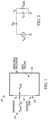
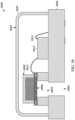
- Pressure microphonestypically include a diaphragm that responds to the pressure difference on either side of it.
- a diaphragmthat responds to the pressure difference on either side of it.
- P atmatmospheric pressure
- P acdesired acoustic signal
- the pressure on the other side of the diaphragm 12is provided by a back volume 16 which is acoustically isolated from the outside environment 14 yet maintains atmospheric pressure in it through a small acoustic leak 15 .
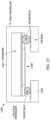
- FIG. 2A small-signal lumped element model for the omnidirectional microphone 10 of FIG. 1 is shown in FIG. 2 .
- the compliance of the diaphragm 12 and the back volume 16are represented by capacitors C D and C BV , respectively.
- the resistance of the acoustic leak 15is represented by R Leak .
- the acoustic signalis represented as an AC signal source.
- P DThe pressure across the diaphragm 12 , P D , causes the diaphragm 12 to move. Notice that the atmospheric pressure, which is present on both sides of the diaphragm 12 , is no factor in the diaphragm motion and is not included in this small signal model.
- the acoustic leakbeing a real resistance, generates thermal noise.
- This noiseappears as a noise pressure across the diaphragm 12 .
- the parallel combination of the back volume compliance (C BV ) and the diaphragm compliance (C D )limits the noise to low frequencies so that when the noise is integrated over the audio frequency range (the noise is band limited so this is equivalent to integrating from zero to infinity), the result is the well known quantity kT/C where k is Boltzmann's constant, T is absolute temperature in Kelvin, and C is the parallel combination of the two compliances (C D and C BV ).
- kT/Cwhere k is Boltzmann's constant, T is absolute temperature in Kelvin, and C is the parallel combination of the two compliances (C D and C BV ).
- thermal resistancecould possibly affect the internal noise of the microphone if the noise from this resistance were comparable to or greater than the other thermal noise sources in the microphone.”
- the thermal-acoustic noise contributionis expected to be greatest for MEMS microphones with small enclosure volumes and low frequencies, where the distances between solid surfaces are on the order of the thickness of the thermal boundary layer within the back volume (which increases with decreasing operating frequency).
- the thermal boundary layer thicknessmay be determined approximately as
- ⁇ t2 ⁇ ⁇ ⁇ ⁇ ⁇ 0 ⁇ C p
- ⁇is the operating angular frequency of the microphone
- ⁇is the thermal conductivity
- ⁇ 0is the density
- C pis the specific heat at constant pressure of the gas inside the microphone assembly (e.g., within the back volume of the microphone assembly).
- the heat exchangeis frequency dependent and contributes to the impedance of the back volume.
- the air in the back volumeis compressed, its temperature rises.
- the portion of the air within a diffusion length of a boundarygives up this heat to the boundary material.
- the air in the back volumerarifies, the temperature of the air drops but the portion of the air within a diffusion length of a boundary gains heat from the boundary material.
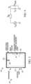
- FIG. 3depicts the thermal boundary layer 18 for the omnidirectional microphone 10 of FIG. 1 .
- the thermal boundary layer 18is shaded to depict how the thickness 20 of the thermal boundary layer 18 changes with frequency. Darker shading corresponds to the thickness 20 at higher frequency. Thus, at high frequencies, the thermal boundary layer 18 is quite thin while at low frequencies, the thermal boundary layer 18 is thicker.
- the impact of the thermal boundary layer 18 on the modelis shown in FIG. 4 .
- the compliance of the back volumeis now replaced with a complex impedance Z BV .
- the real part of the complex impedancedepends on frequency and microphone size and thus a noise contribution is made to the pressure across the diaphragm.
- the analysis of this noise effectis complex but addressed in Kuntzman. In essence, as the microphone gets smaller, the thermal boundary layer expands to consume more of the total back volume and when integrated, the total noise effect on the pressure across the diaphragm goes up as the microphone size goes down. This is another expected kT/C effect.
- a MEMS diee.g., operating as an acoustic transducer
- MEMS dieswhere the distance between any point within the back volume and the nearest solid surface to that point is less than a single thermal boundary layer thickness at an upper limit of the audio frequency band for a MEMS transducer that employs such dies. Because the thermal boundary layer thickness increases with decreasing frequency (as described above), this limit ensures that the distance between any point within the back volume and the nearest solid surface is less than a single thermal boundary layer thickness over a majority of the audio frequency band for the MEMS die.
- the upper limitis an upper frequency of the audio band of interest for detection by the microphone.
- the upper limitmay be an upper range of the frequency band that the integrated circuit is monitoring for the audio signal (e.g., 20 kHz).
- a MEMS diemay react to, and a microphone may detect audio signals above the upper limit.
- the design of the microphonewould be optimized for a given upper limit.
- the phrase “enclosed volume” or “enclosed back volume”refers to a volume (such as a back volume) that is substantially enclosed but may not be fully enclosed.
- the enclosed volumemay refer to a volume that is fluidly connected with an environment surrounding the MEMS die via a pierce or opening in a diaphragm, in a piston, or in a resilient structure.
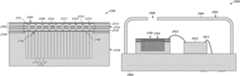
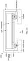
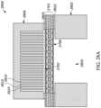
- FIG. 5 and FIG. 6show a side cross-sectional view of a MEMS die 100 for a microphone.
- the MEMS die 100is configured to use a capacitive acoustic transduction method to generate an electrical signal in response to acoustic disturbances incident on the MEMS die 100 .
- the MEMS die 100may be use another type of transduction, such as piezoelectric transduction, piezoresistive transduction, or optical transduction.
- the MEMS die 100includes a substrate 102 , an electrode 104 , and a movable diaphragm 106 .
- the movable diaphragm 106may be or may include an electrode and may be referred to as a “first electrode,” while the electrode 104 may be referred as a “second electrode.”
- the diaphragm 106 and the electrode 104along with the gap therebetween (which includes insulative material such as air), form a capacitive element.
- the electrode 104may sometimes be referred to as a counter electrode.
- the substrate 102supports the electrode 104 and the diaphragm 106 . As shown in FIG. 5 , the electrode 104 is coupled directly to the substrate 102 along an entire lower surface 108 of the electrode 104 .
- the substrate 102is large relative to the diaphragm 106 (and relative to the electrode 104 ), which ensures that the electrode 104 is rigidly supported.
- a combined thickness 109 of the substrate 102 and the electrode 104is an order of magnitude greater than a thickness 112 of the diaphragm 106 .
- the relative thickness between the substrate 102 and the diaphragm 106may be different.
- the electrode 104is deposited directly onto a first surface (e.g., an upper surface) of the substrate 102 .
- the electrode 104is deposited onto or otherwise connected to an insulator 114 .
- the insulator 114may be made from silicon nitride or another dielectric material.
- the electrode 104may be made from polycrystalline silicon or another suitable conductor.
- the electrode 104is “sandwiched” or otherwise disposed between the substrate 102 and the insulator 114 .
- the electrode 104is at least partially embedded within a lower surface of the insulator 114 and is directly coupled to the substrate 102 .
- the position of the electrode 104may be different (e.g., the electrode 104 may be embedded within or formed onto an upper surface of the insulator 114 ).
- the electrode 104may extend to an outer perimeter of the volume between the electrode 104 and the diaphragm 106 (e.g., the diameter of the electrode 104 may be approximately the same as the diameter of the diaphragm 106 .
- the diaphragm 106is oriented parallel (or substantially parallel) to the electrode 104 (or insulator 114 , whichever is on top) and is spaced apart from the electrode 104 to form a gap.
- the gaprepresents a height 118 of a cylindrically-shaped cavity (e.g., a cylindrically-shaped volume between the insulator 114 and the diaphragm 106 , or a cylindrically-shaped volume between the electrode 104 and the diaphragm 106 in those embodiments where the electrode 104 is on top of the insulator 114 ).
- the volume between the electrode 104 and the diaphragm 106forms an entire back volume 103 for the MEMS die 100 (and, to the extent that the MEMS die 100 can be considered to be a microphone, the entire back volume of the microphone) as will be further described.
- the diaphragm 106is spaced apart from the electrode 104 by at least an intermediate layer 120 .
- a first side 122 of the intermediate layer 120is coupled to the insulator 114 , which, in turn, is coupled to electrode 104 .
- a second side 124 of the intermediate layer 120is coupled to the diaphragm 106 along at least a portion of the perimeter of the diaphragm 106 .
- a height 126 of the intermediate layer 120(e.g., an axial height of the intermediate layer 120 parallel to a central axis 128 of the MEMS die 100 ), plus a height/thickness of the insulator 114 between the electrode 104 and the intermediate layer 120 , is approximately equal to a distance between the diaphragm 106 and the electrode 104 (e.g., the height 118 ). In other embodiments, the distance between the diaphragm 106 and the electrode 104 is approximately equal to the height of the intermediate layer 120 .
- the intermediate layer 120includes a sacrificial layer (e.g., an oxide layer, a phosphosilicate glass (PSG) layer, a nitride layer, or any other suitable material) that is deposited or otherwise formed onto the electrode 104 .
- a sacrificial layere.g., an oxide layer, a phosphosilicate glass (PSG) layer, a nitride layer, or any other suitable material
- the intermediate layer 120may be made from silicon oxide or other materials that can be etched without affecting the substrate 102 , the electrode 104 , or the diaphragm 106 .
- the diaphragm 106is made from polycrystalline silicon or another conductive material. In other embodiments, the diaphragm 106 includes both an insulating layer and a conductive layer. As shown in FIG. 6 , a first side 132 of the diaphragm 106 faces the back volume 103 . A second side 134 of the diaphragm 106 , opposing the first side 132 , faces toward a front volume 105 for the microphone assembly. Sound energy 131 (e.g., sound waves, acoustic disturbances, etc.) incident on the second side 134 diaphragm 106 from the front volume 105 causes the diaphragm 106 to move toward or away from the electrode 104 .
- Sound energy 131e.g., sound waves, acoustic disturbances, etc.
- the change in distance between the electrode 104 and the diaphragm 106results in a corresponding change in capacitance.
- An electrical signal representative of the change in capacitancemay be generated and transmitted to portions of a microphone assembly in which the MEMS die 100 is incorporated, such as to an integrated circuit (not shown), for processing.
- the electrode 104is a solid, unperforated structure, such that the volume between the insulator 114 and the diaphragm 106 forms an entire back volume 103 for the MEMS die 100 .
- the back volumeincludes both the volume between the structure opposing the diaphragm (the insulator 114 and, if exposed, the electrode 104 ) and the diaphragm 106 as well as any additional fluid (e.g., air) volume on an opposing side of the opposing structure to which the space between the electrode 104 and the diaphragm 106 is fluidly connected.
- Embodiments of the present disclosuremay also include other types of MEMS dies.
- the MEMS diemay be piezoelectric, piezoresistive, or optically transductive.
- FIG. 7shows an embodiment of a piezoelectric MEMS die 175 .
- the piezoelectric MEMS die 175includes a substrate 177 and a diaphragm 179 coupled to the substrate 177 and spaced apart from the substrate 177 .
- the piezoelectric MEMS die 175also includes a piezoelectric layer 181 connected to the diaphragm 179 . As shown in FIG. 7 , the piezoelectric layer 181 may be connected (e.g., deposited onto or otherwise coupled) to a lower surface 183 of the diaphragm 179 .
- the piezoelectric layer 181may be connected to an upper surface 185 of the diaphragm 179 . In either case, the volume between the substrate 177 and the diaphragm 179 forms an entire back volume 187 for the piezoelectric MEMS die 175 .
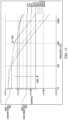
- FIG. 9shows a plot of the A-weighted acoustic noise 200 in the audio frequency band (e.g., range) of 20 Hz to 20 kHz (hereafter “acoustic noise”) of a MEMS die as a function of the size of the back volume of the MEMS die.
- acoustic noisethe A-weighted acoustic noise 200 in the audio frequency band (e.g., range) of 20 Hz to 20 kHz (hereafter “acoustic noise”) of a MEMS die as a function of the size of the back volume of the MEMS die.
- FIG. 9shows the simulated relationship between the acoustic noise 200 and the back volume for a MEMS die with a counter electrode and diaphragm of fixed size (e.g., for a diaphragm with fixed diameter), in which the MEMS die is being used as a transducer.
- the back volumewas varied within a range between approximately 0.0006 mm 3 and 10 mm 3 by changing the size of the gap (e.g., height 118 of FIG. 5 ) between 0.5 um and 8 mm.
- the acoustic noise 200increases with decreasing back volume (e.g., decrease in the height 118 of FIG. 5 ) within a range between approximately 9 mm 3 and 0.1 mm 3 .
- the trend in acoustic noise 200 between approximately 9 mm 3 and 0.1 mm 3is consistent with the discussion provided in both Kuntzman and Thompson, which teach that the acoustic noise increases as the size of the back volume decreases.
- FIG. 10shows a plot of the relationship between the thermal boundary layer thickness 300 and the operating frequency of a MEMS die being used as a transducer (e.g., the MEMS transducer modeled in FIG. 9 , and assuming air is provided within the volume between the counter electrode and the diaphragm).
- the thermal boundary layer thickness 300is shown to decrease with increasing operating frequency. This dependency is shown graphically in FIG. 10 over a range of operating frequencies within the audio frequency band of the MEMS die (e.g., within a human audible frequency range between approximately 20 Hz to 20 kHz).
- the thermal boundary layer thickness 300is less than the size of the gap over a majority of the audio frequency band of the MEMS die. As the gap decreases, the thermal boundary layer thickness 300 becomes equal to or greater than the size of the gap over a larger proportion of the audio frequency band. It is within this range of gap sizes that the thermal-acoustic noise contribution is greatest and the overall SNR of the MEMS die is reduced (e.g., the MEMS die being used as a transducer).
- the approximate range of gap sizes that correspond with improved SNR performanceis identified by horizontal lines 302 toward the bottom of FIG. 10 .
- the size of the gape.g., height 118 shown in FIG. 5
- the boundary layer thickness 300 within the back volume 103 over a majority of the audio frequency band of the MEMS die 100e.g., between 20 Hz and 20 kHz.
- the back volume 103is dimensioned such that the distance between any point or location within the back volume 103 and the nearest solid surface contacting the back volume 103 is less than a single thermal boundary layer thickness 300 .
- a point 119 approximately half way in between the diaphragm 106 and the insulator 114is spaced less than one thermal boundary layer thickness 300 from a back volume facing surface of both the diaphragm 106 and the insulator 114 (the solid surfaces of the back volume that are closest to point 119 ).
- the lower set of curves 404show the damping response for MEMS dies where the size of the gap is less than the thermal boundary layer thickness (e.g., less than two times the thermal boundary layer thickness, similar to the MEMS die 100 of FIG. 5 and FIG. 6 ).
- the direction of decreasing gap size for the curves 404 in FIG. 11is indicated by dashed arrow 406 .
- the damping (and related thermal noise)is shown to decrease as the size of the gap decreases.
- the lower set of curves 404exhibits an approximately flat damping response as a function of frequency. Such properties may be particularly advantageous for applications such as beam forming for signal processing, and other applications where the sensitivity of the MEMS die is reduced at low frequencies.
- FIG. 12shows the acoustic SNR as a function of the gap size for three different values of the surface area of the diaphragm (e.g., the diameter of the diaphragm, and correspondingly, the diameter of the back volume) for a microphone assembly.
- Curves of acoustic SNRare provided over a range of different surface areas for the counter electrode and the diaphragm.
- the acoustic SNRis shown to increase with decreasing gap.
- the acoustic SNRis shown to decrease with decreasing surface area.
- FIGS. 9 - 12were simulated assuming piston-like diaphragm displacement (e.g., assuming that the diaphragm does not curve or bow, and that all points along the surface of the diaphragm move by an equal amount).
- the diaphragm 106(see FIG. 5 ) will not displace uniformly in a piston-like motion but will instead bow or curve under the bias voltage applied to the MEMS die 100 (and further as a result of sound pressure incident on the diaphragm 106 ).
- the movement of the diaphragm 106will therefore move the air within the gap in both an axial direction (e.g., vertically up and down as shown in FIG.
- the radial velocity component of air within the back volume 103will result in viscous losses, which will increase acoustic noise for the MEMS die above the values shown in FIG. 12 .
- FIG. 13shows a plot of the acoustic SNR as a function of the size of the gap between the counter electrode and the diaphragm (the vertical spacing between the counter electrode and the diaphragm).
- Curve 500shows the acoustic SNR for a MEMS die that is modeled assuming a piston-like diaphragm motion.
- Curve 502shows the acoustic SNR for a MEMS die that is modeled assuming that the diaphragm bends (e.g., curves) with the application of a bias voltage to the MEMS die.
- the effect of actual diaphragm bending and movementis most prominent at small gap sizes (e.g., below 5 ⁇ m in this case).
- the bias voltage applied to the MEMS diemay be adjusted (e.g., increased) to increase the sensitivity of the microphone assembly to at least partially offset the effects of the additional acoustic noise resulting from viscous losses.
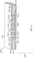
- FIG. 14shows a MEMS die 600 that includes a curved electrode 604 .
- an upper surface 632e.g., first surface, back volume facing surface, etc.
- an upper surface 632 of the insulator 614is shaped to approximately match the curvature of the diaphragm 606 under application of a bias voltage such that, during operation, the distance between the diaphragm 606 and the electrode 604 (which is also curved in this embodiment) is approximately equal throughout the back volume 611 (e.g., in a lateral direction, away from a central axis of the MEMS die).
- the electrode 604 and the diaphragm 606are not parallel in a resting situation (e.g., when the bias voltage is removed). As shown in FIG. 14 , the electrode 604 is deposited or otherwise formed onto a recessed portion 636 of a substrate 602 of the MEMS die 600 . The curvature of the electrode 604 is a function of the bias voltage applied to the MEMS die 600 , the dimensions of the back volume 611 , and the thickness of the diaphragm 606 .
- the MEMS die 100is shown to include an opening or pierce 138 that extends through the diaphragm 106 (e.g., from the first side 132 of the diaphragm 106 to the second side 134 of the diaphragm 106 ).
- the pierce 138is disposed at a central position on the diaphragm 106 in coaxial arrangement relative to the central axis 128 of the MEMS die 100 .
- the pierce 138is a circular through-hole in the diaphragm 106 . In other embodiments, the size, shape, location, and or number of openings in the diaphragm 106 may be different.
- FIG. 15shows the acoustic SNR of a MEMS die (configured like the MEMS die 100 ) as a function of the size of the gap for a range of different diameters for the pierce (e.g., the pierce 138 ).
- the pierceintroduces acoustic noise into the MEMS die 100 (see also FIG. 5 ), particularly at small gap sizes (e.g., below 5 ⁇ m).
- the rate of change (e.g., increase) of the acoustic noisealso increases with the diameter of the pierce.
- the diameter 140 of the pierce 138is within a range between approximately 0.25 ⁇ m and 2 ⁇ m to minimize the effects of the pierce 138 on the overall acoustic SNR. It should be appreciated that the optimal range of pierce 138 diameters will vary depending on the thickness of the diaphragm 106 and the geometry of the back volume 103 .
- the sensitivity of the MEMS die 100may also be improved by increasing the compliance of air in the back volume 103 (e.g., by reducing the stiffness of the air contained within the back volume). In an embodiment, this is accomplished by providing channels in the MEMS substrate, such that every point within the channels is no further away from a solid surface than the thickness of a single thermal boundary layer.
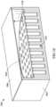
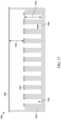
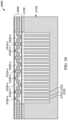
- FIG. 16 and FIG. 17a MEMS die 700 configured accordingly is shown.
- the MEMS die 700includes an electrode 704 and a substrate 702 that includes a plurality of channels 742 formed into the electrode 704 and substrate 702 .
- the MEMS die 700is structured with the channels 742 formed with dimensions such that any point within the channels 742 is less than a single thermal boundary layer thickness from a nearest boundary surface.
- each one of the plurality of channels 742extends away from the diaphragm 706 in a substantially perpendicular orientation relative to the diaphragm 706 (e.g., parallel to a central axis of the MEMS die 700 ).
- the channels 742extend through the electrode 704 .
- the channels 742increase the overall compliance of air within the MEMS die 700 (e.g., by adding air volume away from the space between the electrode 704 and the diaphragm 706 ) without fully penetrating through the substrate 702 .
- the channels 742 in the substrate 702are sized to reduce thermal-acoustic noise within the MEMS die 700 .
- a width 744e.g., diameter
- the depth 745 of each of the channels 742is approximately equal to the size of the gap, shown as height 718 (e.g., the distance between the electrode 704 and the diaphragm 706 ). It will be appreciated that the geometry of the channels 742 may be different in various embodiments. For instance, in other embodiments the depth 745 may be different from the size of the gap.
- channels in a MEMS substratemay be defined by pillars.
- An example of such a MEMS dieis shown in FIG. 18 .
- the MEMS die, generally labelled 750includes an electrode 754 and a substrate 752 forming a cavity 756 (e.g., back volume) in which a plurality of pillars 758 are disposed.
- the pillars 758are cylinders that extend upwardly from a lower surface of the cavity 756 in a substantially perpendicular orientation relative to the lower surface (the pillars 758 extend toward the diaphragm 706 ).
- the shape of the pillars 758may be different.
- the pillars 758may be formed into a substrate 752 for the MEMS die 750 .
- a conductive layer 715is deposited onto or otherwise connected to an upper surface of each one of the pillars 758 . Together, the conductive layers 715 form a single electrode.
- a lateral distance between adjacent pillars 758e.g., a radial distance relative to a central axis of each of the pillars 758 ) is less than two times the thermal boundary layer thickness over a majority of an audio frequency band of the MEMS die 750 .
- the geometry of the channels ( FIG. 16 and FIG. 17 ) and pillars ( FIG. 18 )may be different.
- a porous silicon substratemay be used in lieu of channels or pillars. Among other benefits, using a porous silicon substrate increases the effective compliance of the air within the back volume, without requiring additional manufacturing operations to form channels, pillars, or other geometry into the substrate.
- the MEMS diegenerally labeled 770 , includes a substrate 772 .
- the substrate 772can be doped to make it conductive so that the surface of a porous region 774 is effectively the counter electrode for a capacitive transducer.
- the size of the pores 776is much less than a single thermal boundary layer thickness and yet allows air flow in all directions.
- the percentage of open volume in the porous region 774can be controlled by well-known electrochemical processes and can be made fairly large.
- the gap size, shown as height 778 , between the upper surface of the porous region 774 (e.g., the counter electrode) and the diaphragm 780still must be less than two thermal boundary layer thicknesses, but in this embodiment the gap size does not dominate the size of the back volume 782 and thus the sensitivity of the MEMS die 770 .
- a sintered materialcould be used instead of porous silicon with characteristic pore sizes as described above.
- FIG. 20shows monolithic integration of a MEMS die 800 with an integrated circuit (IC) 802 .
- the IC 802may be an application specific integrated circuit (ASIC).
- the IC 802may include another type of semiconductor die integrating various analog, analog-to-digital, and/or digital circuits. As shown in FIG.
- the IC 802forms a substrate for the MEMS die 800 .
- the MEMS die 800is integrally formed on the IC 802 as a single unitary structure.
- An electrode 804 of the MEMS die 800is directly coupled to IC 802 along an entire lower surface 808 of the electrode 804 .
- the geometry of the electrode 804may be the same or similar to the geometry of the electrode 104 described with reference to FIG. 5 .
- the electrode 804is directly coupled to the IC 802 (e.g., formed onto an upper surface of the IC 802 ).
- the IC 802includes a substrate 810 and an upper portion 812 coupled to a first surface (e.g., an upper surface, etc.) of the substrate 810 .
- the IC 802additionally includes a plurality of transistors 813 embedded in the upper surface of the substrate 810 , between the substrate 810 and the upper portion 812 .
- the upper portion 812is structured to electrically couple (e.g., connect, etc.) the electrode 804 to the IC 802 and/or to other parts of the microphone assembly (not shown).
- the upper portion 812includes a plurality of metal layers 814 embedded within the upper portion 812 .
- the metal layers 814electrically connect the electrode 804 to a contact disposed at an outer surface of the upper portion 812 (e.g., to an outer surface of the combined MEMS die 800 and IC 802 ).
- the combination of the MEMS die 800 and the IC 802 dieis configured to fit within a microphone assembly, shown as assembly 900 .
- the assembly 900includes a housing including a base 902 , a cover 904 (e.g., a housing lid), and a sound port 906 .
- the base 902is a printed circuit board.
- the cover 904is coupled to the base 902 (e.g., the cover 904 may be mounted onto a peripheral edge of the base 902 ). Together, the cover 904 and the base 902 form an enclosed volume for the assembly 900 (e.g., a front volume 910 of the MEMS die 800 ). As shown in FIG.
- the sound port 906is disposed on the cover 904 and is structured to convey sound waves to the MEMS die 800 located within the enclosed volume.
- the sound port 906may be disposed on the base 902 .
- the sound wavese.g., sound pressure, etc.
- move the diaphragm 806 of the MEMS die 800which changes the size of the gap (e.g., the height 818 ) between the diaphragm 806 and the electrode 804 .
- the volume between the electrode 804 and the diaphragm 806forms an entire back volume 911 for the MEMS die 800 , which, advantageously, reduces the overall footprint of the microphone assembly 900 , without limiting the acoustic SNR that can be achieved.
- the substrate 810is coupled to a first surface of the base 902 within the enclosed volume 908 .
- the assemblymay form part of a compact computing device (e.g., a portable communication device, a smartphone, a smart speaker, an internet of things (IoT) device, etc.), where one, two, three or more assemblies may be integrated for picking-up and processing various types of acoustic signals such as speech and music.
- a compact computing devicee.g., a portable communication device, a smartphone, a smart speaker, an internet of things (IoT) device, etc.
- the MEMS die 800is configured to generate an electrical signal (e.g., a voltage) at an output in response to acoustic activity incident on the sound port 906 .
- the outputincludes a pad or terminal of the MEMS die 800 that is electrically connected to the electrical circuit via one or more bonding wires 912 .
- the assembly 900may further include electrical contacts disposed on a surface of the base 902 outside of the cover 904 . The contacts may be electrically coupled to the electrical circuit (e.g. via bonding wires or electrical traces embedded within the base 902 ) and may be configured to electrically connect the microphone assembly 900 to one of a variety of host devices.
- FIG. 22shows another embodiment of a microphone assembly 1000 that includes a MEMS die 1100 that is flip-chip bonded to a base 1002 of the microphone assembly 1000 .
- the MEMS die 1100is separated from the base 1002 (and electrically connected to the base 1002 ) by balls of solder 1003 .
- the MEMS die 1100is arranged to receive sound energy through a sound port 1006 disposed centrally within the base 1002 .
- the MEMS die 1100is suspended within a cavity formed between the base 1002 and a cover 1004 of the microphone assembly 1000 .
- FIG. 23shows another embodiment of a microphone assembly 1200 that is similar to the microphone assembly 1000 of FIG. 22 , but where the cover has been replaced by an encapsulant 1201 that surrounds the MEMS die 1300 .
- the encapsulant 1201insulates the MEMS die 1300 and helps to support the MEMS die 1300 in position above the base 1202 of the microphone assembly 1200 .
- the encapsulantmay include a curable epoxy or any other suitable material.
- a capacitive MEMS sensoruses a piston (e.g., a rigid piece of silicon) in place of a diaphragm.
- the pistonis supported by a resilient structure (e.g., a soft rubber seal, a gasket (made, for example, of PDMS), or a bellowed wall).
- the resilient structureprovides a seal that prevents the lateral movement of air, which reduces noise.
- the MEMS dieincludes a vent that allows pressure in the back volume to equalize with the ambient pressure (but only at non-acoustic frequencies—it is sealed at acoustic frequencies).
- the MEMS die 2400includes a piston 2402 that is rigid (e.g., made of relatively thick silicon) and conductive (e.g., made of a conductive material such as a metal or a doped semiconductor (such as crystalline silicon)), an electrode 2404 facing the piston 2402 , and a resilient structure 2406 that supports the piston 2402 on the electrode 2404 .
- a back volume 2408is bounded on top by the piston 2402 , bounded on the bottom by the electrode 2404 , and bounded on all sides by the resilient structure 2406 .
- the piston 2402 , electrode 2404 , and the resilient structure 2406enclose a back volume 2408 .
- the electrode 2404is part of a substrate that also includes insulative material that supports the electrode 2404 .
- the resilient structure 2406prevents air or other gas from leaving the back volume 2408 (e.g., blocks the air or other gas from travelling in direction radially outward from a central portion of the back volume 2408 ). Put another way, the resilient structure 2406 seals the back volume 2408 to prevent lateral velocity gradients in the captured air volume.
- Possible implementations of the resilient structure 2406include a gasket made of polydimethylsiloxane (PDMS) or rubber.
- the resilient structure 2406is a pleated wall (made of, for example, PDMS, rubber, or made of more rigid materials such as silicon, silicon nitride, or aluminum).
- An example of a suitable structure having a pleated wallis a flexible bellow seal.
- Yet another possible implementation of the resilient structure 2406is a thin diaphragm at the perimeter.
- the piston 2402has a vent 2411 that allows pressure between the back volume 2408 and the area external to the MEMS die 2400 to be equalized when the piston 2402 is at rest or is moving up and down relative to the electrode 2404 at non-acoustic frequencies.
- the vent 2411is a hole that is configured to permit pressure equalization between the back volume and a region (e.g., a volume) external to the MEMS die at frequencies below the audio band.
- the vent 2411may have a geometry and dimensions that result in an impedance that the vent 2411 has no impact on the flow of air at non-audio frequencies but which blocks flow of air at acoustic frequencies.
- the vent 2411need not be located in the piston 2402 , but may be anywhere (e.g., in the resilient structure 2406 ) to facilitate pressure equalization.
- the piston 2402 and the electrode 2404form a capacitive element, with the piston 2402 serving as a first electrode of the capacitive element, the electrode 2404 serving as a second electrode of the capacitive element, and the air or other gas in the back volume 2408 acting as a dielectric.
- the piston 2402 and the resilient structure 2406behave like a classic spring-mass system.
- the capacitance between the piston 2402 and the electrode 2404changes as the distance between them changes (i.e., as distance increases or decreases).
- the resilient structure 2406resists the movement of the piston 2402 towards the electrode (e.g., in response to incoming pressure waves, such as those produced by sound).
- the piston 2402when the MEMS die 2400 is integrated into a microphone, the piston 2402 is electrically connected to a bias voltage source 2409 and the electrode 2404 is electrically connected to an integrated circuit 2410 (e.g., to an amplifier input thereof).
- the piston 2402may be electrically connected to the integrated circuit 2410 and the electrode 2404 may be electrically connected to the bias voltage source 2409 .
- the MEMS die 2450includes a piston 2403 that has an insulative portion 2403 a and an electrode 2403 b .
- itis the electrode 2403 b that functions as the first electrode in the capacitive element (with the electrode 2404 acting as the second electrode).
- channels 2412are formed into the electrode 2404 of FIG. 24 A and FIG. 24 B .
- the dimensions of the channels 2412are such that any point within the channels 2412 is less than a single thermal boundary layer thickness from a nearest surface.
- Each of the channels 2412extends away from the piston 2402 in a substantially perpendicular orientation relative to the piston 2402 (e.g., parallel to a central axis of the MEMS die).
- the channels 2412increase the overall compliance of air within the MEMS die (e.g., by adding air volume away from the space between the electrode and the piston) without fully penetrating through electrode 2404 .
- the space within the channels 2412is part of the back volume.
- FIG. 24 Ca perspective view of the electrode 2404 of FIG. 24 A (after the MEMS die 2400 is cross sectioned along line A-A′) according to an embodiment is shown.
- pillars 2414are formed into the electrode 2404 and the spaces between the pillars 2414 constitute the channels 2412 .
- the channels 2412 and the pillars 2414may be of any shape as long as any point within the channel is less than a thermal boundary layer thickness from a surface of a pillar 2414 at the upper limit of audio frequency.
- FIG. 24 Da top view of the electrode 2404 of FIG. 24 A (after the MEMS die 2400 is cross sectioned along line A-A′) according to another embodiment is shown.
- the channels 2412are formed in the electrode 2404 in concentric rings.
- the electrode facing the pistonis part of a layered structure generally referred to as a substrate, which may include, for example, a layer of polycrystalline silicon and a layer of insulator, with the electrode being embedded in the substrate (e.g., within the insulative material) or disposed on the surface of the substrate (e.g., on top of the insulative material).
- a MEMS dieconfigured according to such an embodiment is shown.
- the MEMS die 2500includes a piston 2502 , which is configured like the piston 2402 of FIG. 24 A and has the same possible variations, including a distinct electrode and insulative material.
- the MEMS die 2500further includes a substrate 2504 , and a resilient structure 2506 that supports the piston 2502 on the substrate 2504 .
- Possible implementations of the piston 2502 and the resilient structure 2506include those discussed in conjunction with piston and resilient structures of FIG. 24 A and FIG. 24 B .
- a back volume 2508is bounded on top by the piston 2502 , bounded on the bottom by the substrate 2504 , and bounded on all sides by the resilient structure 2506 .
- the piston 2502 , substrate 2504 , and the resilient structure 2506enclose a back volume 2508 .
- the resilient structure 2506prevents air from leaving the back volume 2508 , and particularly blocks air from travelling in a direction radially outward from a central portion of the back volume 2508 .
- the substrate 2504includes an insulative layer 2510 (made, for example, of silicon dioxide or silicon nitride) and an electrode 2512 that is embedded in the insulative layer 2510 .
- the electrode 2512faces the piston 2502 such that a capacitance exists between the piston 2502 and the electrode 2512 (with the piston 2502 acting as a first electrode of a capacitor, the electrode 2512 acting as a second electrode of the capacitor, and the air or other gas in the back volume 2508 acting as the dielectric).
- the piston 2502includes both insulative material and a conductive portion or layer, in which the conductive portion or layer acts as the first electrode of the capacitor.
- the piston 2502when the MEMS die 2500 is integrated into a microphone, the piston 2502 is electrically connected to a bias voltage source 2514 and the electrode 2512 is electrically connected to an integrated circuit 2516 (e.g., to an amplifier input thereof). Alternatively, the piston 2502 may be electrically connected to the integrated circuit 2516 and the electrode 2512 may be electrically connected to the bias voltage source 2514 .
- channels 2518are formed into the substrate 2504 , and the electrode 2512 spans the channels 2518 .
- the dimensions of the channels 2518are such that any point within the channels 2518 is less than a single thermal boundary layer thickness from a nearest surface.
- each of the channels 2518extends away from the piston 2502 in a substantially perpendicular orientation relative to the piston 2502 (e.g., parallel to a central axis of the MEMS die 2500 ).
- the channels 2518extend through the electrode 2512 .
- the channels 2516increase the overall compliance of air within the MEMS die 2500 (e.g., by adding air volume away from the space between the second electrode 2512 and the piston 2502 ) without fully penetrating through the substrate 2504 .
- the space within the channels 2518is part of the back volume 2508 .
- the MEMS die 2500includes walls 2520 and one or more external conductors 2522 .
- Each external conductor 2522is electrically connected to the piston 2502 (or to an electrode on the piston 2502 if the piston includes insulative material) at one end and to a wall 2520 at the other end.
- each of the one or more external conductors 2522is a resilient member, such as a metallic spring.
- the walls 2520are connected to the bias voltage source 2514 by way of a contact 2524 (e.g., a eutectic metal contact) and a conductive path 2526 within the insulative layer 2510 of the substrate 2504 (with through-silicon vias (TSVs) as appropriate).
- FIG. 25 Bdepicts the walls 2520 and the external conductors 2522 as seen from above the piston 2502 .
- the function of the electrode 2512may be carried out by two electrodes, shown in the MEMS die 2550 of FIG. 25 C .
- the function of the electrode 2512is carried out by an electrode 2512 a and an electrode 2512 b , both of which are depicted as being embedded in the substrate 2504 (in the insulative layer 2510 ).
- the electrode 2512 ais electrically connected to the bias voltage source 2514 via a conductive path 2526 a and the electrode 2512 b is electrically connected to the integrated circuit 2516 (e.g., to an amplifier input thereof) via a conductive path 2526 b.
- the pistonis connected to an electrical potential through a very large resistor.
- the electrical potentialmay be electrical ground.
- the resistance of the resistorshould be large enough to set the electrical corner frequency below that of the desired low acoustic corner frequency (e.g. 20 Hz).
- the resistancemay be 10 ⁇ circumflex over ( ) ⁇ 12 ohm. In other embodiments, the resistance may be less or more than 10 ⁇ circumflex over ( ) ⁇ 12 ohm.
- the resistoris formed by the electrical leakage conductance of resilient structure 2506 b and insulative layer 2510 . In operation, the piston is connected to an electrical potential in a DC sense, but is electrically isolated in the AC sense.
- FIG. 25 D(which is a variation on the embodiment described in conjunction with FIG. 25 C ).
- a MEMS die 2560has the piston 2502 configured to be electrically floating.
- the electrode 2512 ais connected to the bias voltage source 2414 via a conductive path 2526 a and the electrode 2412 b is connected to the integrated circuit 2416 (e.g., to an amplifier input thereof) via a conductive path 2526 b.
- FIG. 25 Ea partial perspective view of the substrate 2504 cross sectioned along line B-B′ (of FIG. 25 A ) according to an embodiment is shown.
- pillars 2530are formed into the substrate 2504 and the spaces between the pillars 2530 constitute the channels 2518 .
- At least some of the pillarsinclude an electrically conductive layer 2532 that is connected (e.g., with a TSV down the long axis of the pillar) to a single, common conductor so that all of the electrically conductive layers are part of the electrode 2512 .
- This substrate configurationmay also be used in the embodiments of FIG. 25 C and FIG. 25 D , but with two electrically separate conductive layers instead of the single electrically conductive layer 2522 that is shown in FIG. 25 E .
- FIG. 25 Fa top view of the substrate 2504 cross sectioned along line C-C′ (of FIG. 25 A ) according to another embodiment is shown.
- the channels 2518are formed into the substrate 2504 in rings, such as the concentric rings shown in FIG. 25 F between parts of the electrode 2512 , which is also formed in concentric rings 2536 .
- a single conductive rib 2534electrically connects the rings 2536 of the electrode 2512 .
- This substrate configurationmay also be used in the embodiments of FIG. 25 C and FIG. 25 D , but with two separate electrodes (e.g., with two separate conductive ribs).
- channelsare provided in the piston to increase the compliance of the air in the back volume.
- FIG. 26 Aa MEMS die configured according to such an embodiment is shown.
- the MEMS die 2600includes a piston 2602 that is rigid (e.g., made of relatively thick silicon) and that is conductive (e.g., a semiconductor like crystalline silicon), a substrate 2604 , and a resilient structure 2606 that supports the piston 2602 on the substrate 2604 .
- Possible implementations of the piston 2602 and the resilient structure 2606include those discussed in conjunction with the piston 2402 and the resilient structure 2406 of FIG. 24 A .
- the piston 2602 , substrate 2604 , and the resilient structure 2606enclose a back volume 2608 .
- the resilient structure 2606blocks air from leaving the back volume 2608 , and particularly blocks air from travelling in a direction radially outward from a central portion of the back volume 2608 .
- the substrate 2604includes an insulative layer 2610 (made, for example, of silicon dioxide) and an electrode 2612 that is embedded in the insulative layer 2610 .
- the electrode 2612faces the piston 2602 such that a capacitance exists between the piston 2602 and the electrode 2612 (with the piston 2602 acting as a first electrode of a capacitor, the electrode 2612 acting as a second electrode of the capacitor, and the air or other gas in the back volume 2608 acting as the dielectric).
- the piston 2602includes both insulative material and a conductive portion or layer, in which the conductive portion or layer acts as the first electrode of the capacitor.
- the piston 2602when the MEMS die 2600 is integrated into a microphone, the piston 2602 is electrically connected to a bias voltage source 2614 (e.g., via external conductors 2622 ) and the electrode 2612 is electrically connected to an integrated circuit 2616 (e.g., to an amplifier input thereof) (e.g., via a conductive path 2622 ).
- the piston 2602may be electrically connected to the integrated circuit 2616 and the electrode 2612 may be electrically connected to the bias voltage source 2614 .
- the piston 2602includes channels 2618 .
- the space within the channels 2618is part of the back volume 2608 .
- the dimensions of the channels 2618are such that any point within the channels 2618 is less than a single thermal boundary layer thickness from a nearest surface.
- each of the channels 2618extends away from the substrate 2604 in a substantially perpendicular orientation relative to the substrate 2604 (e.g., parallel to a central axis of the MEMS die 2600 ).
- the channels 2618increase the overall compliance of air within the MEMS die 2600 (e.g., by adding air volume away from the space between the substrate 2604 ) without fully penetrating through the piston 2602 .
- FIG. 26 Bshows a partial perspective view of a cross section of the piston 2602 along line D-D′.
- pillars 2624are formed into the piston 2602 and the spaces between the pillars 2624 constitute the channels 2618 .
- FIG. 26 Ca bottom view of the piston 2602 cross sectioned along line D-D′ according to another embodiment is shown.
- the channels 2618are formed into the piston 2602 in concentric rings.
- the function of the electrode 2612may be carried out by two electrodes, as shown in the MEMS die 2650 of FIG. 26 D .
- the functions of the electrode 2612are carried out by an electrode 2612 a and an electrode 2612 b .
- the electrode 2612 ais connected to the bias voltage source 2614 and the electrode 2612 b is connected to the integrated circuit 2616 (e.g., to an amplifier input thereof) via respective conductive pathways 2622 a and 2622 b.
- the piston 2602may be electrically floating, as shown in the MEMS die 2660 of FIG. 26 E .
- the electrode 2612 ais connected to the bias voltage source 2614 via a conductive path 2622 a and the electrode 2612 b is connected to the integrated circuit 2616 (e.g., to an amplifier input thereof) via a conductive path 2622 b.
- the MEMS diemay also include a resilient structure inside the back volume (e.g., near a central axis of the MEMS die).
- a resilient structureis in addition to a resilient structure at the periphery of the piston.
- FIG. 26 FAn example of such an embodiment is shown in FIG. 26 F , in which a MEMS die 2670 is configured like the MEMS die 2600 of FIG. 26 A except that the MEMS die 2670 includes a second resilient structure 2607 inside the back volume 2608 .
- One possible advantage to the second resilient structure 2607is that it may increase the resonance frequency for the MEMS die 2670 to limit adverse effects that would result from having the resonance in or near the audio band.
- a MEMS die 2700includes a dual-diaphragm diaphragm assembly 2701 .
- the dual-diaphragm assembly 2701includes a first diaphragm 2702 comprising a first electrode 2704 , a second diaphragm 2706 comprising a second electrode 2708 , and a backplate 2710 comprising a third electrode 2712 .
- the first diaphragm 2702 and the second diaphragm 2706are oriented so that they face one another, and the backplate 2710 is disposed in between the first diaphragm 2702 and the second diaphragm 2706 and facing both the first diaphragm 2702 and the second diaphragm 2706 .
- the first diaphragm 2702 and the second diaphragm 2706are connected to one another by pillars 2713 , which extend through the backplate 2710 .
- the MEMS die 2700further includes a spacer 2714 that is sandwiched between and connected to the first diaphragm 2702 and the backplate 2710 , and a spacer 2716 that is sandwiched between and connected to the second diaphragm 2706 and the backplate 2710 .
- a region 2716 between the first diaphragm 2702 and the second diaphragm 2706is sealed off and is at a lower pressure than standard atmospheric pressure (e.g., 50% atmospheric pressure) and may be at or near a vacuum.
- the MEMS die 2700further includes an enclosure 2718 that is formed from and acts as a substrate.
- the second diaphragm 2706is attached to the enclosure 2718 via a spacer 2720 .
- channels 2722are formed into the enclosure 2718 .
- the dimensions of the channels 2722are such that any point within the channels 2722 is less than a single thermal boundary layer thickness from a nearest surface.
- the channels 2722increase the overall compliance of air within the MEMS die 2700 .
- the space within the channels 2722is part of the back volume. Possible configurations for the topography of the substrate 2718 include those discussed in conjunction with FIG. 24 C and FIG. 24 D with pillars or rings, respectively.
- the MEMS die 2800includes the dial-diaphragm assembly 2701 of FIG. 27 , but with a substrate, labeled 2802 . Attached to the first diaphragm 2702 (via a spacer 2805 ) is an enclosure 2806 . Channels 2810 are formed into the enclosure 2806 . In an embodiment, the dimensions of the channels 2810 are such that any point within the channels 2810 is less than a single thermal boundary layer thickness from a nearest surface. The space within the channels 2810 is part of the back volume. Possible configurations for the topography of the enclosure 2806 include those discussed in conjunction with FIG. 26 B and FIG. 26 C with pillars or rings, respectively.
- the substrate 2802has a hole 2820 through which sound passes.
- the second diaphragm 2706is attached to the substrate 2802 via a spacer 2822 .
- a variation of the MEMS die 2800is shown in FIG. 28 B .
- a MEMS die 2850includes the enclosure 2806 and the substrate 2802 . Additionally, the MEMS die 2850 has a single diaphragm 2852 and a backplate 2854 facing the diaphragm 2852 .
- the diaphragm 2852has a first electrode 2856 and the backplate 2854 has a second electrode 2858 .
- the diaphragm 2852is attached to the enclosure 2806 via a spacer 2860 .
- the backplate 2854is attached to the diaphragm 2852 via a spacer 2862 and to the substrate 2802 via a spacer 2864 .
- sound enters the hole 2820passes through the backplate 2854 and strikes the diaphragm 2852 .
- FIG. 28 CAnother variation of the MEMS die 2800 is shown in FIG. 28 C .
- the MEMS die 2870is similar to the MEMS die 2850 of FIG. 28 B except that the positions of the backplate 2854 and the diaphragm 2852 are reversed and there is a second backplate 2862 that has an electrode 2864 .
- FIG. 29an example use of the MEMS die 2700 of FIG. 27 is depicted in the context of a sensor, specifically an acoustic sensor referred to as a microphone 2900 .
- the microphone 2900has a housing 2902 that includes a can 2904 and a base 2906 .
- the can 2904is attached to the base 2906 .
- Pressure wavese.g., sound waves
- the distance between the first electrode 2704 and the third electrode 2712altering the capacitance between the first electrode 2704 and third electrode 2712 .
- the distance between the second electrode 2708 and the third electrode 2712changes, altering the capacitance between the second electrode 2708 and the third electrode 2712 .
- These capacitance changesare read by an electrical circuit (e.g., integrated circuit) 2910 , which is attached to MEMS die 2700 via one or more signal pathways (e.g., wires) 2912 .
- the electrical circuit 2910interprets the signals representing the capacitance changes and interprets the signals as, for example, sound.
- the electrical circuitthen provides further signals representing the interpretation via one or more additional signal pathways (e.g., wires) to external devices.
- FIG. 30an example use of the MEMS die 2800 is depicted in the context of a sensor, specifically an acoustic sensor referred to as a microphone 3000 .
- the microphone 3000has a housing 3002 that includes a can 3004 and a base 3006 .
- the can 3004is attached to the base 3006 .
- Pressure waves(e.g., sound waves) enter a port 3008 on the base 3006 , pass through the hole 2820 in the substrate 2802 and strike the second diaphragm 2806 , cause it to flex and to induce corresponding flexion in the first diaphragm 2802 (via the pillars 2813 ).
- the distance between the first electrode 2804 and the third electrode 2812altering the capacitance between the first electrode 2804 and third electrode 2812 .
- the distance between the second electrode 2808 and the third electrode 2812changes, altering the capacitance between the second electrode 2808 and the third electrode 2812 .
- These capacitance changesare read by an electrical circuit (e.g., integrated circuit) 3010 , which is attached to MEMS die 2800 via one or more signal pathways (e.g., wires) 3012 .
- the electrical circuit 3010interprets the signals representing the capacitance changes and interprets the signals as, for example, sound.
- the electrical circuitthen provides further signals representing the interpretation via one or more additional signal pathways (e.g., wires) to external devices.
- dual-diaphragm assembliesmay also be used in place of the dual-diaphragm assembly 2701 of FIG. 27 , FIG. 28 A , FIG. 29 , and FIG. 30 .
- a dielectric motor MEMS assemblymay be used. The principles of such an assembly according to an embodiment will now be described with reference to FIG. 31 A , FIG. 31 B , and FIG. 32 .
- a dielectric motor MEMS device 3100includes a first electrode 3110 oriented lengthwise along and parallel to an axis 3160 .
- the first electrode 3110has a first end 3111 and a second end 3112 .
- the MEMS device 3100also includes a second electrode 3120 oriented lengthwise along and parallel to the axis 3160 .
- the second electrode 3120has a first end 3121 and a second end 3122 .
- the MEMS device 3100further includes a third electrode 3130 oriented lengthwise along and parallel to the axis 3160 .
- the third electrode 3130has a first end 3131 and a second end 3132 .
- the electrodes 3110 , 3120 , and 3130may be cylinders, plates, cuboids, prisms, polyhedrons, or other shapes of electrodes.
- the length of the first electrode 3110is longer than the length of the second electrode 3120 and longer than the length of the third electrode 3130 .
- the MEMS device 3100has a solid dielectric 3150 interspersed among the electrodes.
- the dielectric 3150may be made, for example, of silicon nitride.
- the electrodes 3110 , 3120 , and 3130are made of a conductor or a semiconductor, such as plated metals or poly silicon.
- the first electrode 3110is an electrically conductive pin of a plurality of first electrically conductive pins electrically connected to each other
- the second electrode 3120is an electrically conductive pin of a plurality of second electrically conductive pins electrically connected to each other
- the third electrode 3130is an electrically conductive pin of a plurality of third electrically conductive pins electrically connected to each other.
- the dielectric 3150has a plurality of apertures 3156 that penetrate through the dielectric 3150 in a direction parallel to an axis 3160 .
- the apertures 3156are depicted as cylindrical but may be any suitable shape.
- the first, second, and third electrodescan each be located at least partially within an aperture of the plurality of apertures 3156 . In other words, part of an electrode may be located within an aperture and/or the electrode may be located in part of the aperture. According to a possible embodiment, at least the second and third electrodes are located only partially within the apertures 3156 for the ends to be located outside the dielectric 3150 .
- the first electrode 3110may be disposed at least partially within a first aperture of the plurality of apertures 3156 .
- the second end 3122 of the second electrode 3120may be disposed within a second aperture of the plurality of apertures 3156 .
- the first end 3131 of the third electrode 3130may be disposed within a third aperture of the plurality of apertures 3156 .
- the dielectric 3150has a first surface 3151 and a second surface 3152 .
- the first surface 3151 and the second surface 3152are parallel to a plane perpendicular to the axis 3160 .
- the first end 3111 of the first electrode 3110 and the first end 3121 of the second electrode 3120extend beyond the first surface 3151
- the second ends 3112 and 3132 of the respective first and third electrodes 3110 and 3130extend beyond the second surface 3152 .
- the electrodes of the device 3100are substantially fixed relative to each other.
- the electrodesmay allow for some minor relative movement with respect to one another due to flexion and other forces.
- the dielectric 3150 and electrodesmay also be free to move relative to each other.
- the dielectric 3150may be movable parallel to the axis 3160 relative to the first, second, and third electrodes. Additionally or alternatively, the first, second, and third electrodes may be movable relative to the dielectric 3150 .
- the dielectric 3150may also take other forms such as one or more segments or members.
- the dielectric 3150can fill at least 50% of a distance (e.g., a distance perpendicular to the first length of the first electrode 3110 ) between the first and second electrode 3120 .
- the dielectric 3150may fill at least 75% of the distance, at least 80% of the distance, or at least between 80-90% of the distance.
- the dielectric 3150may fill any amount from 1% to 99% of the distance. The more the dielectric fills the gap between the electrodes, the more the capacitance changes per unit of displacement and thus the higher the force generated for a given voltage bias between electrodes. Some minimal gap should remain between the dielectric and the electrodes, subject to fabrication constraints, so that the dielectric and electrodes remain moveable relative to each other.
- a first capacitanceexists between the first electrode 3110 and the second electrode 3120 and a second capacitance exists between the first electrode 3110 and the third electrode 3130 .
- the capacitance between electrodesis a function of their positions relative to the dielectric 3150 .
- values of the first and second capacitancecan change in opposite directions when the dielectric 3150 moves relative to the electrodes in a direction parallel to the axis 3160 .
- the second capacitancemay simultaneously decrease.
- An electrostatic force on the dielectric 3150 relative to the electrodes 3110 , 3120 , and 3130may, however, be substantially unchanged relative to the displacement.
- a voltage from a first voltage source V 1is applied between the first electrode 3110 and the second electrode 3120 producing a relatively constant force F 1 .
- a voltage from a second voltage source V 2is applied between the first electrode 3110 and the third electrode 3130 to produce a relatively constant force F 2 .
- Forces F 1 and F 2are in opposition. If the structure is relatively symmetric and the magnitude of the voltage sources V 1 and V 2 are equal, forces F 1 and F 2 are equal and thus a net zero force is exerted between the dielectric and the electrodes.
- the magnitude of the voltages from the voltage sources V 1 and V 2can be unequal to compensate for asymmetries in the structure or to intentionally create a non-zero net force between the dielectric and the electrodes.
- FIG. 32a dielectric motor MEMS device 3200 according to another embodiment will now be described.
- the function of the first electrode 3110(from FIG. 3 A and FIG. 3 B ) is carried out by a first set of electrically interconnected electrodes 3210 - x
- the function of the second electrode 3120is carried out by a second set of electrically interconnected electrodes 3220 - x
- the function of the third electrode 3130is carried out by a third set of electrically interconnected electrodes 3230 - x
- the second and third sets of electrodes 3220 - x and 3230 - xcan be staggered on either side of the first set of electrodes 3210 - x . This allows for more capacitance and an increase in the change of capacitance with displacement.
- Other configurations of conductive and dielectric elements, such as bars or rings,may also be used.
- the dual-diaphragm assembly 3300includes a diaphragm 3370 coupled to the first set of electrodes 3210 - x and the third set of electrodes 3230 - x .
- the diaphragm 3370has a surface 3372 perpendicular to the axis 3360 .
- the surface 3372is substantially planar (e.g., planar but with imperfections on the surface 3372 or slightly curved or uneven while still allowing the surface 3372 to operate in a manner useful for a diaphragm).
- the diaphragm 3370may be made of sandwiched layers.
- the dual-diaphragm assembly 3300also includes a second diaphragm 3374 located on an opposite side of the dielectric 3350 from the first diaphragm 3370 .
- the second diaphragm 3374is coupled to the first set of electrodes 3210 - x and the second set of electrodes 3220 - x .
- the second diaphragm 3374has substantially planar surface 3376 and is oriented perpendicular to the axis 3360 .
- the first diaphragm 3370 and the second diaphragm 3374are spaced from the dielectric 3350 to permit relative movement between the electrodes connected to the first and second diaphragms and the dielectric 3350 .
- a sealed low-pressure regionis defined between the diaphragms 3370 and 3374 .
- This low-pressure regionserves to reduce noise and damping of the assembly 3300 .
- the first set of electrodes 3210 - x(which are connected to both the first diaphragm 3370 and the second diaphragm 3374 ) help prevent the diaphragms from collapsing onto the dielectric 3350 .
- This low-pressure regionmay be substantially a vacuum (e.g., with a pressure less than 1 Torr, less than 300 mTorr, or less than 100 mTorr).
- the dielectric 3350is relatively thick and stiff compared to the diaphragms 3370 and 3374 and remains relatively motionless when the diaphragms 3370 and 3374 are deflected. Deflection of the diaphragms 3370 and 3374 moves the electrodes 3210 - x , 3220 - x , and 3230 - x relative to the dielectric 3350
- the diaphragms 3370 and 3374may be made of a dielectric material, such as silicon nitride. However, other materials can be used. For example, one or more of the diaphragm 3370 , the diaphragm 3374 , and the dielectric 3150 can be polyimide.
- the MEMS die 3300operates as follows. Pressure (e.g., from sound waves) reaches at least one of the diaphragms, causing it to flex and to move the electrodes attached thereto relative to the dielectric, thereby causing respective capacitances between the various elements to change. This change in capacitance manifests as a change in one or more signals being output from the MEMS die 3300 .
- the one or more signalsare read and interpreted by an IC and passed on to other external components.
- FIG. 34depicts a MEMS device 3400 that includes all of the elements of the MEMS device 2700 from FIG. 27 but with the dual-diaphragm assembly 2701 replaced by the dual-diaphragm dielectric motor assembly 3300 .
- the MEMS device 3400otherwise functions similarly to the MEMS device 2700 .
- FIG. 35depicts an embodiment in which a MEMS device 3500 includes all of the elements of the MEMS device 2800 from FIG. 28 A but with the dual diaphragm-assembly 2701 replaced by the dual-diaphragm dielectric motor assembly 3300 .
- the MEMS device 3500otherwise functions similarly to the MEMS device 2800 .
Landscapes
- Engineering & Computer Science (AREA)
- Physics & Mathematics (AREA)
- Acoustics & Sound (AREA)
- Signal Processing (AREA)
- Computer Hardware Design (AREA)
- Microelectronics & Electronic Packaging (AREA)
- Multimedia (AREA)
- Chemical & Material Sciences (AREA)
- Analytical Chemistry (AREA)
- Electrostatic, Electromagnetic, Magneto- Strictive, And Variable-Resistance Transducers (AREA)
Abstract
Description
where ω is the operating angular frequency of the microphone, and where κ is the thermal conductivity, ρ0is the density, and Cpis the specific heat at constant pressure of the gas inside the microphone assembly (e.g., within the back volume of the microphone assembly). The relationship above confirms the dependency between the thermal boundary layer thickness and the operating frequency of the microphone.
Claims (19)
Priority Applications (4)
| Application Number | Priority Date | Filing Date | Title |
|---|---|---|---|
| US17/207,722US12240748B2 (en) | 2021-03-21 | 2021-03-21 | MEMS die and MEMS-based sensor |
| DE102022106135.3ADE102022106135A1 (en) | 2021-03-21 | 2022-03-16 | MEMS DIE AND MEMS BASED SENSOR |
| CN202210263170.3ACN115119120B (en) | 2021-03-21 | 2022-03-17 | MEMS dies and MEMS-based sensors |
| US18/600,185US20240208802A1 (en) | 2021-03-21 | 2024-03-08 | Mems die and mems-based sensor |
Applications Claiming Priority (1)
| Application Number | Priority Date | Filing Date | Title |
|---|---|---|---|
| US17/207,722US12240748B2 (en) | 2021-03-21 | 2021-03-21 | MEMS die and MEMS-based sensor |
Related Child Applications (1)
| Application Number | Title | Priority Date | Filing Date |
|---|---|---|---|
| US18/600,185DivisionUS20240208802A1 (en) | 2021-03-21 | 2024-03-08 | Mems die and mems-based sensor |
Publications (2)
| Publication Number | Publication Date |
|---|---|
| US20220298005A1 US20220298005A1 (en) | 2022-09-22 |
| US12240748B2true US12240748B2 (en) | 2025-03-04 |
Family
ID=83114960
Family Applications (2)
| Application Number | Title | Priority Date | Filing Date |
|---|---|---|---|
| US17/207,722Active2042-08-20US12240748B2 (en) | 2021-03-21 | 2021-03-21 | MEMS die and MEMS-based sensor |
| US18/600,185PendingUS20240208802A1 (en) | 2021-03-21 | 2024-03-08 | Mems die and mems-based sensor |
Family Applications After (1)
| Application Number | Title | Priority Date | Filing Date |
|---|---|---|---|
| US18/600,185PendingUS20240208802A1 (en) | 2021-03-21 | 2024-03-08 | Mems die and mems-based sensor |
Country Status (3)
| Country | Link |
|---|---|
| US (2) | US12240748B2 (en) |
| CN (1) | CN115119120B (en) |
| DE (1) | DE102022106135A1 (en) |
Families Citing this family (6)
| Publication number | Priority date | Publication date | Assignee | Title |
|---|---|---|---|---|
| DE102021205736A1 (en)* | 2021-06-08 | 2022-12-08 | Robert Bosch Gesellschaft mit beschränkter Haftung | Micromechanical component for a sensor device |
| US20230106456A1 (en)* | 2021-10-06 | 2023-04-06 | Knowles Electronics, Llc | Mems die and mems-based sensor |
| DE102022214252A1 (en) | 2022-12-21 | 2024-06-27 | Robert Bosch Gesellschaft mit beschränkter Haftung | Converter unit for electrical and/or acoustic signals and/or relative pressures |
| DE102022214250A1 (en)* | 2022-12-21 | 2024-06-27 | Robert Bosch Gesellschaft mit beschränkter Haftung | Converter unit for acoustic or electrical signals or relative pressures |
| DE102023211179A1 (en)* | 2023-11-10 | 2025-05-15 | Robert Bosch Gesellschaft mit beschränkter Haftung | Microelectromechanical pressure sensor and method for producing a microelectromechanical pressure sensor |
| WO2025188419A1 (en)* | 2024-03-07 | 2025-09-12 | Invensense, Inc. | Sealed cavity for a capacitive sensing device |
Citations (134)
| Publication number | Priority date | Publication date | Assignee | Title |
|---|---|---|---|---|
| US4154115A (en) | 1976-06-08 | 1979-05-15 | Akademie Der Wissenschaften Ddr | Method and device for continuous measuring of gas pressures |
| US4435986A (en) | 1980-11-12 | 1984-03-13 | Centre Electronique Horloger S.A. | Pressure transducer of the vibrating element type |
| US5575310A (en) | 1986-03-04 | 1996-11-19 | Deka Products Limited Partnership | Flow control system with volume-measuring system using a resonatable mass |
| US6075867A (en) | 1995-06-23 | 2000-06-13 | Microtronic A/S | Micromechanical microphone |
| US6431003B1 (en) | 2000-03-22 | 2002-08-13 | Rosemount Aerospace Inc. | Capacitive differential pressure sensor with coupled diaphragms |
| US6435033B2 (en) | 1997-04-17 | 2002-08-20 | Commissariat A L'energie Atomique | Process for manufacturing a microsystem with a flexible membrane for a pressure sensor |
| US6535460B2 (en) | 2000-08-11 | 2003-03-18 | Knowles Electronics, Llc | Miniature broadband acoustic transducer |
| US6571445B2 (en) | 1999-05-20 | 2003-06-03 | Igal Ladabaum | Method for making acoustic transducer |
| US6662663B2 (en) | 2002-04-10 | 2003-12-16 | Hewlett-Packard Development Company, L.P. | Pressure sensor with two membranes forming a capacitor |
| US20050177045A1 (en) | 2004-02-06 | 2005-08-11 | Georgia Tech Research Corporation | cMUT devices and fabrication methods |
| US20050207605A1 (en) | 2004-03-08 | 2005-09-22 | Infineon Technologies Ag | Microphone and method of producing a microphone |
| US20050219953A1 (en) | 2004-04-06 | 2005-10-06 | The Board Of Trustees Of The Leland Stanford Junior University | Method and system for operating capacitive membrane ultrasonic transducers |
| KR100571967B1 (en) | 2000-08-11 | 2006-04-18 | 노우레스 일렉트로닉스, 엘엘시 | Mini broadband converter |
| US7030407B2 (en) | 2001-06-20 | 2006-04-18 | Infineon Technologies Ag | Photon emitter and data transmission device |
| US7040173B2 (en) | 2004-03-08 | 2006-05-09 | Infineon Technologies Ag | Pressure sensor and method for operating a pressure sensor |
| US7124638B2 (en) | 2003-07-01 | 2006-10-24 | Infineon Technologies Ag | Pressure sensor and method for detecting an effective pressure |
| US7150195B2 (en) | 2003-10-10 | 2006-12-19 | Infineon Technologies Sensonor As | Sealed capacitive sensor for physical measurements |
| US7190038B2 (en) | 2001-12-11 | 2007-03-13 | Infineon Technologies Ag | Micromechanical sensors and methods of manufacturing same |
| US20070205492A1 (en) | 2006-03-03 | 2007-09-06 | Silicon Matrix, Pte. Ltd. | MEMS microphone with a stacked PCB package and method of producing the same |
| US20070278501A1 (en) | 2004-12-30 | 2007-12-06 | Macpherson Charles D | Electronic device including a guest material within a layer and a process for forming the same |
| US20080175425A1 (en) | 2006-11-30 | 2008-07-24 | Analog Devices, Inc. | Microphone System with Silicon Microphone Secured to Package Lid |
| US20080267431A1 (en) | 2005-02-24 | 2008-10-30 | Epcos Ag | Mems Microphone |
| US20080279407A1 (en) | 2005-11-10 | 2008-11-13 | Epcos Ag | Mems Microphone, Production Method and Method for Installing |
| US20080283942A1 (en) | 2007-05-15 | 2008-11-20 | Industrial Technology Research Institute | Package and packaging assembly of microelectromechanical sysyem microphone |
| US7470546B2 (en) | 2000-05-31 | 2008-12-30 | Infineon Technologies Ag | Method and arrangement for taking up a first medium, which is present in a first phase, into a capillary device |
| US20090001553A1 (en) | 2005-11-10 | 2009-01-01 | Epcos Ag | Mems Package and Method for the Production Thereof |
| US7489593B2 (en) | 2004-11-30 | 2009-02-10 | Vermon | Electrostatic membranes for sensors, ultrasonic transducers incorporating such membranes, and manufacturing methods therefor |
| US7535156B2 (en) | 2006-03-28 | 2009-05-19 | Infineon Technologies Sensonor As | Energy scavenger and method for manufacturing the same |
| US7545012B2 (en) | 2004-12-27 | 2009-06-09 | General Electric Company | Capacitive micromachined ultrasound transducer fabricated with epitaxial silicon membrane |
| US20090175477A1 (en) | 2007-08-20 | 2009-07-09 | Yamaha Corporation | Vibration transducer |
| US20090180655A1 (en) | 2008-01-10 | 2009-07-16 | Lingsen Precision Industries, Ltd. | Package for mems microphone |
| US20100046780A1 (en) | 2006-05-09 | 2010-02-25 | Bse Co., Ltd. | Directional silicon condensor microphone having additional back chamber |
| US20100052082A1 (en) | 2008-09-03 | 2010-03-04 | Solid State System Co., Ltd. | Micro-electro-mechanical systems (mems) package and method for forming the mems package |
| US20100128914A1 (en) | 2008-11-26 | 2010-05-27 | Analog Devices, Inc. | Side-ported MEMS microphone assembly |
| US20100164025A1 (en) | 2008-06-25 | 2010-07-01 | Yang Xiao Charles | Method and structure of monolithetically integrated micromachined microphone using ic foundry-compatiable processes |
| US20100170346A1 (en) | 2009-01-07 | 2010-07-08 | Bernhard Opitz | Sensor element for capacitive differential-pressure sensing |
| US20100173437A1 (en) | 2008-10-21 | 2010-07-08 | Wygant Ira O | Method of fabricating CMUTs that generate low-frequency and high-intensity ultrasound |
| US20100183181A1 (en) | 2009-01-20 | 2010-07-22 | General Mems Corporation | Miniature mems condenser microphone packages and fabrication method thereof |
| US7781249B2 (en) | 2006-03-20 | 2010-08-24 | Wolfson Microelectronics Plc | MEMS process and device |
| US7793550B2 (en) | 2008-08-25 | 2010-09-14 | Infineon Technologies Ag | Sensor device including two sensors embedded in a mold material |
| US7795695B2 (en) | 2005-01-27 | 2010-09-14 | Analog Devices, Inc. | Integrated microphone |
| US20100246877A1 (en) | 2009-01-20 | 2010-09-30 | Fortemedia, Inc. | Miniature MEMS Condenser Microphone Package and Fabrication Method Thereof |
| US7825484B2 (en) | 2005-04-25 | 2010-11-02 | Analog Devices, Inc. | Micromachined microphone and multisensor and method for producing same |
| US7829961B2 (en) | 2007-01-10 | 2010-11-09 | Advanced Semiconductor Engineering, Inc. | MEMS microphone package and method thereof |
| US20100290644A1 (en) | 2009-05-15 | 2010-11-18 | Aac Acoustic Technologies (Shenzhen) Co., Ltd | Silicon based capacitive microphone |
| US20100322451A1 (en) | 2009-06-19 | 2010-12-23 | Aac Acoustic Technologies (Shenzhen) Co., Ltd | MEMS Microphone |
| US20100322443A1 (en) | 2009-06-19 | 2010-12-23 | Aac Acoustic Technologies (Shenzhen) Co., Ltd | Mems microphone |
| US20110013787A1 (en) | 2009-07-16 | 2011-01-20 | Hon Hai Precision Industry Co., Ltd. | Mems microphone package and mehtod for making same |
| US7903831B2 (en) | 2005-08-20 | 2011-03-08 | Bse Co., Ltd. | Silicon based condenser microphone and packaging method for the same |
| US20110075875A1 (en) | 2009-09-28 | 2011-03-31 | Aac Acoustic Technologies (Shenzhen) Co., Ltd | Mems microphone package |
| US7918135B2 (en) | 2009-02-03 | 2011-04-05 | Infineon Technologies Ag | Pressure sensor including thermal selftest |
| US8127619B2 (en) | 2009-01-16 | 2012-03-06 | Infineon Technologies Ag | Pressure sensor including switchable sensor elements |
| US20120087521A1 (en) | 2010-10-12 | 2012-04-12 | Analog Devices, Inc. | Microphone Package with Embedded ASIC |
| WO2012085335A1 (en) | 2010-12-21 | 2012-06-28 | Teknologian Tutkimuskeskus Vtt | Method for manufacturing an ultrasonic sensor and a sensor structure |
| US8339764B2 (en) | 2008-05-12 | 2012-12-25 | Nxp B.V. | MEMs devices |
| US20120328132A1 (en) | 2011-06-27 | 2012-12-27 | Yunlong Wang | Perforated Miniature Silicon Microphone |
| US20130001550A1 (en) | 2011-06-29 | 2013-01-03 | Invensense, Inc. | Hermetically sealed mems device with a portion exposed to the environment with vertically integrated electronics |
| US20130094675A1 (en) | 2011-10-12 | 2013-04-18 | Electronics And Telecommunications Research Institute | Mems microphone and method of manufacturing the same |
| US8461655B2 (en) | 2011-03-31 | 2013-06-11 | Infineon Technologies Ag | Micromechanical sound transducer having a membrane support with tapered surface |
| CN103344377A (en) | 2013-07-16 | 2013-10-09 | 东南大学 | Capacitive barometric sensor of micro electro mechanical system |
| US8575037B2 (en) | 2010-12-27 | 2013-11-05 | Infineon Technologies Ag | Method for fabricating a cavity structure, for fabricating a cavity structure for a semiconductor structure and a semiconductor microphone fabricated by the same |
| US8650963B2 (en) | 2011-08-15 | 2014-02-18 | Pgs Geophysical As | Electrostatically coupled pressure sensor |
| US20140071642A1 (en) | 2012-09-11 | 2014-03-13 | Horst Theuss | Low stress component package |
| US8723277B2 (en) | 2012-02-29 | 2014-05-13 | Infineon Technologies Ag | Tunable MEMS device and method of making a tunable MEMS device |
| US8809973B2 (en) | 2013-01-23 | 2014-08-19 | Infineon Technologies Ag | Chip package comprising a microphone structure and a method of manufacturing the same |
| US20150001647A1 (en) | 2013-06-28 | 2015-01-01 | Infineon Technologies Ag | MEMS Microphone with Low Pressure Region Between Diaphragm and Counter Electrode |
| US8989411B2 (en) | 2011-04-08 | 2015-03-24 | Board Of Regents, The University Of Texas System | Differential microphone with sealed backside cavities and diaphragms coupled to a rocking structure thereby providing resistance to deflection under atmospheric pressure and providing a directional response to sound pressure |
| US20150090043A1 (en) | 2013-09-27 | 2015-04-02 | Infineon Technologies Ag | Mems |
| US20150110291A1 (en) | 2013-10-17 | 2015-04-23 | Knowles Electronics Llc | Differential High Impedance Apparatus |
| US9031266B2 (en) | 2011-10-11 | 2015-05-12 | Infineon Technologies Ag | Electrostatic loudspeaker with membrane performing out-of-plane displacement |
| US20150247879A1 (en) | 2014-03-03 | 2015-09-03 | Infineon Technologies Ag | Acceleration sensor |
| US9131319B2 (en) | 2012-10-11 | 2015-09-08 | Robert Bosch Gmbh | Component having a micromechanical microphone structure |
| US20150296307A1 (en) | 2014-04-10 | 2015-10-15 | Knowles Electronics, Llc. | Dual diaphragm and dual back plate acoustic apparatus |
| US9179221B2 (en) | 2013-07-18 | 2015-11-03 | Infineon Technologies Ag | MEMS devices, interface circuits, and methods of making thereof |
| US9237402B2 (en) | 2013-08-30 | 2016-01-12 | Knowles Electronics Llc | Integrated CMOS/MEMS microphone die |
| US20160096726A1 (en) | 2012-04-04 | 2016-04-07 | Infineon Technologies Ag | MEMS Device and Method of Making a MEMS Device |
| US9321630B2 (en) | 2013-02-20 | 2016-04-26 | Pgs Geophysical As | Sensor with vacuum-sealed cavity |
| US9332330B2 (en) | 2013-07-22 | 2016-05-03 | Infineon Technologies Ag | Surface mountable microphone package, a microphone arrangement, a mobile phone and a method for recording microphone signals |
| US9380381B2 (en) | 2014-03-18 | 2016-06-28 | Infineon Technologies Ag | Microphone package and method for providing a microphone package |
| US9383282B2 (en) | 2011-05-04 | 2016-07-05 | Ams International Ag | MEMS capacitive pressure sensor, operating method and manufacturing method |
| US9383285B2 (en) | 2012-09-25 | 2016-07-05 | Ams International Ag | MEMS resonator pressure sensor |
| US9425757B2 (en) | 2013-05-15 | 2016-08-23 | Infineon Technologies Ag | Apparatus and method for controlling an amplification gain of an amplifier, and a digitizer circuit and microphone assembly |
| US9432759B2 (en) | 2013-07-22 | 2016-08-30 | Infineon Technologies Ag | Surface mountable microphone package, a microphone arrangement, a mobile phone and a method for recording microphone signals |
| US9438979B2 (en) | 2014-03-06 | 2016-09-06 | Infineon Technologies Ag | MEMS sensor structure for sensing pressure waves and a change in ambient pressure |
| US9503814B2 (en) | 2013-04-10 | 2016-11-22 | Knowles Electronics, Llc | Differential outputs in multiple motor MEMS devices |
| CN106162476A (en) | 2015-04-20 | 2016-11-23 | 钰太芯微电子科技(上海)有限公司 | The mike monomer of anti-low frequency noise |
| US9510107B2 (en) | 2014-03-06 | 2016-11-29 | Infineon Technologies Ag | Double diaphragm MEMS microphone without a backplate element |
| CN205754849U (en) | 2016-05-17 | 2016-11-30 | 歌尔股份有限公司 | A kind of Electret Condencer Microphone chip |
| US9516428B2 (en) | 2013-03-14 | 2016-12-06 | Infineon Technologies Ag | MEMS acoustic transducer, MEMS microphone, MEMS microspeaker, array of speakers and method for manufacturing an acoustic transducer |
| US9549263B2 (en) | 2013-09-13 | 2017-01-17 | Omron Corporation | Acoustic transducer and microphone |
| US9550211B2 (en) | 2011-04-13 | 2017-01-24 | Koninklijke Philips N.V. | Temperature compensation in a CMUT device |
| US9631996B2 (en) | 2014-07-03 | 2017-04-25 | Infineon Technologies Ag | Motion detection using pressure sensing |
| US9641137B2 (en) | 2013-07-10 | 2017-05-02 | Ams Ag | Electric amplifier circuit for amplifying an output signal of a microphone |
| CN206212271U (en) | 2016-11-18 | 2017-05-31 | 北京卓锐微技术有限公司 | Mems structure |
| US9689770B2 (en) | 2014-07-17 | 2017-06-27 | Infineon Technologies Ag | Selfcalibration of capacitive pressure sensors with electrostatic forces |
| US9828237B2 (en) | 2016-03-10 | 2017-11-28 | Infineon Technologies Ag | MEMS device and MEMS vacuum microphone |
| US9884757B2 (en) | 2010-07-13 | 2018-02-06 | Infineon Technologies Ag | MEMS sensor package systems and methods |
| US9903779B2 (en) | 2015-02-09 | 2018-02-27 | Infineon Technologies Ag | Sensor network supporting self-calibration of pressure sensors |
| US20180091906A1 (en) | 2016-09-26 | 2018-03-29 | Cirrus Logic International Semiconductor Ltd. | Mems device and process |
| US9942677B2 (en) | 2014-09-15 | 2018-04-10 | Infineon Technologies Ag | System and method for a transducer |
| WO2018125839A1 (en) | 2016-12-28 | 2018-07-05 | Knowles Electronics, Llc | Microelectromechanical system microphone |
| US20180234774A1 (en) | 2017-02-16 | 2018-08-16 | Infineon Technologies Ag | Microelectromechanical microphone |
| CN108551646A (en) | 2018-06-25 | 2018-09-18 | 歌尔股份有限公司 | Mems microphone |
| US20180317022A1 (en) | 2017-05-01 | 2018-11-01 | Apple Inc. | Combined ambient pressure and acoustic mems sensor |
| US10129676B2 (en) | 2016-02-16 | 2018-11-13 | Infineon Technologies Ag | MEMS microphone, apparatus comprising a MEMS microphone and method for fabricating a MEMS microphone |
| US10153740B2 (en) | 2016-07-11 | 2018-12-11 | Knowles Electronics, Llc | Split signal differential MEMS microphone |
| US10231061B2 (en) | 2017-04-28 | 2019-03-12 | Infineon Technologies Ag | Sound transducer with housing and MEMS structure |
| US20190100429A1 (en) | 2017-09-29 | 2019-04-04 | Cirrus Logic International Semiconductor Ltd. | Mems devices and processes |
| US20190112182A1 (en) | 2017-10-18 | 2019-04-18 | Infineon Technologies Ag | Method for sealing an access opening to a cavity and mems component comprising a sealing element |
| US20190181776A1 (en) | 2016-01-11 | 2019-06-13 | Infineon Technologies Ag | System and Method for a MEMS Device |
| US10322481B2 (en) | 2014-03-06 | 2019-06-18 | Infineon Technologies Ag | Support structure and method of forming a support structure |
| US10362408B2 (en) | 2016-02-04 | 2019-07-23 | Knowles Electronics, Llc | Differential MEMS microphone |
| US20190246459A1 (en) | 2018-02-08 | 2019-08-08 | Infineon Technologies Ag | Emitter structure and production method |
| US10405106B2 (en) | 2015-11-19 | 2019-09-03 | Knowles Electronics, Llc | Differential MEMS microphone |
| US20190270639A1 (en) | 2018-03-01 | 2019-09-05 | Infineon Technologies Ag | MEMS-Sensor |
| WO2019183283A2 (en) | 2018-03-21 | 2019-09-26 | Knowles Electronics, Llc | Dielectric comb for mems device |
| US10433070B2 (en) | 2018-03-02 | 2019-10-01 | Infineon Technologies Ag | Sensitivity compensation for capacitive MEMS device |
| US20190331531A1 (en) | 2018-04-30 | 2019-10-31 | Infineon Technologies Ag | Fluid sensor and method for providing same |
| US20190339193A1 (en) | 2018-05-04 | 2019-11-07 | Infineon Technologies Ag | Photoacoustic gas sensors and method of operating a photoacoustic gas sensor |
| US20190352175A1 (en) | 2018-05-16 | 2019-11-21 | Infineon Technologies Ag | Mems sensor, mems sensor system and method for producing a mems sensor system |
| US20190363757A1 (en) | 2018-05-23 | 2019-11-28 | Infineon Technologies Ag | MultiPolymer Sensor Array Utilizing NFC |
| US10560771B2 (en) | 2017-08-18 | 2020-02-11 | Infineon Technologies Ag | Microelectromechanical microphone |
| US20200057031A1 (en) | 2018-08-17 | 2020-02-20 | Infineon Technologies Ag | Detector module for a photo-acoustic gas sensor |
| US10582306B2 (en) | 2017-03-01 | 2020-03-03 | Infineon Technologies Ag | Capacitive MEMS device, capacitive MEMS sound transducer, method for forming a capacitive MEMS device, and method for operating a capacitive MEMS device |
| US10589990B2 (en) | 2017-09-19 | 2020-03-17 | Infineon Technologies Ag | MEMS microphone |
| US20200112799A1 (en) | 2018-10-05 | 2020-04-09 | Knowles Electronics, Llc | Acoustic transducers with a low pressure zone and diaphragms having enhanced compliance |
| US10641626B2 (en) | 2017-08-23 | 2020-05-05 | Infineon Technologies Ag | MEMS sensors, methods for providing same and method for measuring a fluid constituent |
| US10669151B2 (en) | 2017-09-01 | 2020-06-02 | Infineon Technologies Ag | Double-membrane MEMS component and production method for a double-membrane MEMS component |
| US10676346B2 (en) | 2017-09-22 | 2020-06-09 | Infineon Technologies Ag | MEMS component and production method for a MEMS component |
| US10689250B2 (en) | 2017-07-21 | 2020-06-23 | Infineon Technologies Ag | MEMS component and production method for a MEMS component |
| US10715926B2 (en) | 2017-12-29 | 2020-07-14 | Infineon Technologies Ag | MEMS component and mobile device comprising the MEMS component |
| US20200252729A1 (en) | 2019-02-06 | 2020-08-06 | Simon Mueller | Sensor arrangement and method for providing a sensor signal |
| US20200252728A1 (en) | 2019-02-06 | 2020-08-06 | Mark Niederberger | Sensor arrangement and method |
| CN112689228A (en) | 2019-10-18 | 2021-04-20 | 美商楼氏电子有限公司 | Ultra-miniature microphone |
Family Cites Families (7)
| Publication number | Priority date | Publication date | Assignee | Title |
|---|---|---|---|---|
| JP2012119831A (en)* | 2010-11-30 | 2012-06-21 | Ingen Msl:Kk | Ultrasonic vibrator unit and ultrasonic probe |
| WO2018091690A1 (en)* | 2016-11-18 | 2018-05-24 | Robert Bosch Gmbh | Mems microphone system having an electrode assembly |
| IT201600121533A1 (en)* | 2016-11-30 | 2018-05-30 | St Microelectronics Srl | MEMS INTEGRATED ELECTROACOUSTIC TRANSDUCER WITH IMPROVED SENSITIVITY AND RELATIVE PROCESS OF MANUFACTURING |
| US10825628B2 (en)* | 2017-07-17 | 2020-11-03 | Analog Devices Global Unlimited Company | Electromagnetically actuated microelectromechanical switch |
| JP6503032B2 (en)* | 2017-09-14 | 2019-04-17 | 株式会社東芝 | Sensor device |
| EP3628990B1 (en)* | 2018-09-26 | 2021-08-25 | ams International AG | Integrated optical transducer and method for detecting dynamic pressure changes |
| US11420866B2 (en)* | 2020-03-23 | 2022-08-23 | Taiwan Semiconductor Manufacturing Company, Ltd. | Composite spring structure to reinforce mechanical robustness of a MEMS device |
- 2021
- 2021-03-21USUS17/207,722patent/US12240748B2/enactiveActive
- 2022
- 2022-03-16DEDE102022106135.3Apatent/DE102022106135A1/enactivePending
- 2022-03-17CNCN202210263170.3Apatent/CN115119120B/enactiveActive
- 2024
- 2024-03-08USUS18/600,185patent/US20240208802A1/enactivePending
Patent Citations (157)
| Publication number | Priority date | Publication date | Assignee | Title |
|---|---|---|---|---|
| US4154115A (en) | 1976-06-08 | 1979-05-15 | Akademie Der Wissenschaften Ddr | Method and device for continuous measuring of gas pressures |
| US4435986A (en) | 1980-11-12 | 1984-03-13 | Centre Electronique Horloger S.A. | Pressure transducer of the vibrating element type |
| US5575310A (en) | 1986-03-04 | 1996-11-19 | Deka Products Limited Partnership | Flow control system with volume-measuring system using a resonatable mass |
| US6075867A (en) | 1995-06-23 | 2000-06-13 | Microtronic A/S | Micromechanical microphone |
| US6435033B2 (en) | 1997-04-17 | 2002-08-20 | Commissariat A L'energie Atomique | Process for manufacturing a microsystem with a flexible membrane for a pressure sensor |
| US6571445B2 (en) | 1999-05-20 | 2003-06-03 | Igal Ladabaum | Method for making acoustic transducer |
| US6431003B1 (en) | 2000-03-22 | 2002-08-13 | Rosemount Aerospace Inc. | Capacitive differential pressure sensor with coupled diaphragms |
| US7470546B2 (en) | 2000-05-31 | 2008-12-30 | Infineon Technologies Ag | Method and arrangement for taking up a first medium, which is present in a first phase, into a capillary device |
| KR100571967B1 (en) | 2000-08-11 | 2006-04-18 | 노우레스 일렉트로닉스, 엘엘시 | Mini broadband converter |
| US6535460B2 (en) | 2000-08-11 | 2003-03-18 | Knowles Electronics, Llc | Miniature broadband acoustic transducer |
| US7030407B2 (en) | 2001-06-20 | 2006-04-18 | Infineon Technologies Ag | Photon emitter and data transmission device |
| US7473572B2 (en) | 2001-12-11 | 2009-01-06 | Infineon Technologies Ag | Micromechanical sensors and methods of manufacturing same |
| US7190038B2 (en) | 2001-12-11 | 2007-03-13 | Infineon Technologies Ag | Micromechanical sensors and methods of manufacturing same |
| US6662663B2 (en) | 2002-04-10 | 2003-12-16 | Hewlett-Packard Development Company, L.P. | Pressure sensor with two membranes forming a capacitor |
| US7124638B2 (en) | 2003-07-01 | 2006-10-24 | Infineon Technologies Ag | Pressure sensor and method for detecting an effective pressure |
| US7150195B2 (en) | 2003-10-10 | 2006-12-19 | Infineon Technologies Sensonor As | Sealed capacitive sensor for physical measurements |
| US20050177045A1 (en) | 2004-02-06 | 2005-08-11 | Georgia Tech Research Corporation | cMUT devices and fabrication methods |
| US7040173B2 (en) | 2004-03-08 | 2006-05-09 | Infineon Technologies Ag | Pressure sensor and method for operating a pressure sensor |
| US20050207605A1 (en) | 2004-03-08 | 2005-09-22 | Infineon Technologies Ag | Microphone and method of producing a microphone |
| US20050219953A1 (en) | 2004-04-06 | 2005-10-06 | The Board Of Trustees Of The Leland Stanford Junior University | Method and system for operating capacitive membrane ultrasonic transducers |
| US7489593B2 (en) | 2004-11-30 | 2009-02-10 | Vermon | Electrostatic membranes for sensors, ultrasonic transducers incorporating such membranes, and manufacturing methods therefor |
| US7545012B2 (en) | 2004-12-27 | 2009-06-09 | General Electric Company | Capacitive micromachined ultrasound transducer fabricated with epitaxial silicon membrane |
| US20070278501A1 (en) | 2004-12-30 | 2007-12-06 | Macpherson Charles D | Electronic device including a guest material within a layer and a process for forming the same |
| US7795695B2 (en) | 2005-01-27 | 2010-09-14 | Analog Devices, Inc. | Integrated microphone |
| US20080267431A1 (en) | 2005-02-24 | 2008-10-30 | Epcos Ag | Mems Microphone |
| US7825484B2 (en) | 2005-04-25 | 2010-11-02 | Analog Devices, Inc. | Micromachined microphone and multisensor and method for producing same |
| US7903831B2 (en) | 2005-08-20 | 2011-03-08 | Bse Co., Ltd. | Silicon based condenser microphone and packaging method for the same |
| US20080279407A1 (en) | 2005-11-10 | 2008-11-13 | Epcos Ag | Mems Microphone, Production Method and Method for Installing |
| US20090001553A1 (en) | 2005-11-10 | 2009-01-01 | Epcos Ag | Mems Package and Method for the Production Thereof |
| US20070205492A1 (en) | 2006-03-03 | 2007-09-06 | Silicon Matrix, Pte. Ltd. | MEMS microphone with a stacked PCB package and method of producing the same |
| US7781249B2 (en) | 2006-03-20 | 2010-08-24 | Wolfson Microelectronics Plc | MEMS process and device |
| US7856804B2 (en) | 2006-03-20 | 2010-12-28 | Wolfson Microelectronics Plc | MEMS process and device |
| US7535156B2 (en) | 2006-03-28 | 2009-05-19 | Infineon Technologies Sensonor As | Energy scavenger and method for manufacturing the same |
| US20100046780A1 (en) | 2006-05-09 | 2010-02-25 | Bse Co., Ltd. | Directional silicon condensor microphone having additional back chamber |
| US20080175425A1 (en) | 2006-11-30 | 2008-07-24 | Analog Devices, Inc. | Microphone System with Silicon Microphone Secured to Package Lid |
| US7829961B2 (en) | 2007-01-10 | 2010-11-09 | Advanced Semiconductor Engineering, Inc. | MEMS microphone package and method thereof |
| US20080283942A1 (en) | 2007-05-15 | 2008-11-20 | Industrial Technology Research Institute | Package and packaging assembly of microelectromechanical sysyem microphone |
| US20090175477A1 (en) | 2007-08-20 | 2009-07-09 | Yamaha Corporation | Vibration transducer |
| US20090180655A1 (en) | 2008-01-10 | 2009-07-16 | Lingsen Precision Industries, Ltd. | Package for mems microphone |
| US8339764B2 (en) | 2008-05-12 | 2012-12-25 | Nxp B.V. | MEMs devices |
| US20100164025A1 (en) | 2008-06-25 | 2010-07-01 | Yang Xiao Charles | Method and structure of monolithetically integrated micromachined microphone using ic foundry-compatiable processes |
| US7793550B2 (en) | 2008-08-25 | 2010-09-14 | Infineon Technologies Ag | Sensor device including two sensors embedded in a mold material |
| US20100052082A1 (en) | 2008-09-03 | 2010-03-04 | Solid State System Co., Ltd. | Micro-electro-mechanical systems (mems) package and method for forming the mems package |
| US20100173437A1 (en) | 2008-10-21 | 2010-07-08 | Wygant Ira O | Method of fabricating CMUTs that generate low-frequency and high-intensity ultrasound |
| US20100128914A1 (en) | 2008-11-26 | 2010-05-27 | Analog Devices, Inc. | Side-ported MEMS microphone assembly |
| US20100170346A1 (en) | 2009-01-07 | 2010-07-08 | Bernhard Opitz | Sensor element for capacitive differential-pressure sensing |
| US8127619B2 (en) | 2009-01-16 | 2012-03-06 | Infineon Technologies Ag | Pressure sensor including switchable sensor elements |
| US20100246877A1 (en) | 2009-01-20 | 2010-09-30 | Fortemedia, Inc. | Miniature MEMS Condenser Microphone Package and Fabrication Method Thereof |
| US20100183181A1 (en) | 2009-01-20 | 2010-07-22 | General Mems Corporation | Miniature mems condenser microphone packages and fabrication method thereof |
| US7918135B2 (en) | 2009-02-03 | 2011-04-05 | Infineon Technologies Ag | Pressure sensor including thermal selftest |
| US20100290644A1 (en) | 2009-05-15 | 2010-11-18 | Aac Acoustic Technologies (Shenzhen) Co., Ltd | Silicon based capacitive microphone |
| US20100322443A1 (en) | 2009-06-19 | 2010-12-23 | Aac Acoustic Technologies (Shenzhen) Co., Ltd | Mems microphone |
| US20100322451A1 (en) | 2009-06-19 | 2010-12-23 | Aac Acoustic Technologies (Shenzhen) Co., Ltd | MEMS Microphone |
| US20110013787A1 (en) | 2009-07-16 | 2011-01-20 | Hon Hai Precision Industry Co., Ltd. | Mems microphone package and mehtod for making same |
| US20110075875A1 (en) | 2009-09-28 | 2011-03-31 | Aac Acoustic Technologies (Shenzhen) Co., Ltd | Mems microphone package |
| US9884757B2 (en) | 2010-07-13 | 2018-02-06 | Infineon Technologies Ag | MEMS sensor package systems and methods |
| US20120087521A1 (en) | 2010-10-12 | 2012-04-12 | Analog Devices, Inc. | Microphone Package with Embedded ASIC |
| WO2012085335A1 (en) | 2010-12-21 | 2012-06-28 | Teknologian Tutkimuskeskus Vtt | Method for manufacturing an ultrasonic sensor and a sensor structure |
| US9363609B2 (en) | 2010-12-27 | 2016-06-07 | Infineon Technologies Ag | Method for fabricating a cavity structure, for fabricating a cavity structure for a semiconductor structure and a semiconductor microphone fabricated by the same |
| US8575037B2 (en) | 2010-12-27 | 2013-11-05 | Infineon Technologies Ag | Method for fabricating a cavity structure, for fabricating a cavity structure for a semiconductor structure and a semiconductor microphone fabricated by the same |
| US8461655B2 (en) | 2011-03-31 | 2013-06-11 | Infineon Technologies Ag | Micromechanical sound transducer having a membrane support with tapered surface |
| US8989411B2 (en) | 2011-04-08 | 2015-03-24 | Board Of Regents, The University Of Texas System | Differential microphone with sealed backside cavities and diaphragms coupled to a rocking structure thereby providing resistance to deflection under atmospheric pressure and providing a directional response to sound pressure |
| US9550211B2 (en) | 2011-04-13 | 2017-01-24 | Koninklijke Philips N.V. | Temperature compensation in a CMUT device |
| US9383282B2 (en) | 2011-05-04 | 2016-07-05 | Ams International Ag | MEMS capacitive pressure sensor, operating method and manufacturing method |
| US20120328132A1 (en) | 2011-06-27 | 2012-12-27 | Yunlong Wang | Perforated Miniature Silicon Microphone |
| US20130001550A1 (en) | 2011-06-29 | 2013-01-03 | Invensense, Inc. | Hermetically sealed mems device with a portion exposed to the environment with vertically integrated electronics |
| US8650963B2 (en) | 2011-08-15 | 2014-02-18 | Pgs Geophysical As | Electrostatically coupled pressure sensor |
| US9031266B2 (en) | 2011-10-11 | 2015-05-12 | Infineon Technologies Ag | Electrostatic loudspeaker with membrane performing out-of-plane displacement |
| US20130094675A1 (en) | 2011-10-12 | 2013-04-18 | Electronics And Telecommunications Research Institute | Mems microphone and method of manufacturing the same |
| US8723277B2 (en) | 2012-02-29 | 2014-05-13 | Infineon Technologies Ag | Tunable MEMS device and method of making a tunable MEMS device |
| US20160096726A1 (en) | 2012-04-04 | 2016-04-07 | Infineon Technologies Ag | MEMS Device and Method of Making a MEMS Device |
| US20140071642A1 (en) | 2012-09-11 | 2014-03-13 | Horst Theuss | Low stress component package |
| US9383285B2 (en) | 2012-09-25 | 2016-07-05 | Ams International Ag | MEMS resonator pressure sensor |
| US9131319B2 (en) | 2012-10-11 | 2015-09-08 | Robert Bosch Gmbh | Component having a micromechanical microphone structure |
| US8809973B2 (en) | 2013-01-23 | 2014-08-19 | Infineon Technologies Ag | Chip package comprising a microphone structure and a method of manufacturing the same |
| US9290379B2 (en) | 2013-01-23 | 2016-03-22 | Infineon Technologies Ag | Chip package including a microphone structure and a method of manufacturing the same |
| US9321630B2 (en) | 2013-02-20 | 2016-04-26 | Pgs Geophysical As | Sensor with vacuum-sealed cavity |
| US9516428B2 (en) | 2013-03-14 | 2016-12-06 | Infineon Technologies Ag | MEMS acoustic transducer, MEMS microphone, MEMS microspeaker, array of speakers and method for manufacturing an acoustic transducer |
| US9503814B2 (en) | 2013-04-10 | 2016-11-22 | Knowles Electronics, Llc | Differential outputs in multiple motor MEMS devices |
| US9425757B2 (en) | 2013-05-15 | 2016-08-23 | Infineon Technologies Ag | Apparatus and method for controlling an amplification gain of an amplifier, and a digitizer circuit and microphone assembly |
| US20160066099A1 (en) | 2013-06-28 | 2016-03-03 | Infineon Technologies Ag | MEMS Microphone with Low Pressure Region between Diaphragm and Counter Electrode |
| US9181080B2 (en) | 2013-06-28 | 2015-11-10 | Infineon Technologies Ag | MEMS microphone with low pressure region between diaphragm and counter electrode |
| US9986344B2 (en) | 2013-06-28 | 2018-05-29 | Infineon Technologies Ag | MEMS microphone with low pressure region between diaphragm and counter electrode |
| US20150001647A1 (en) | 2013-06-28 | 2015-01-01 | Infineon Technologies Ag | MEMS Microphone with Low Pressure Region Between Diaphragm and Counter Electrode |
| US9641137B2 (en) | 2013-07-10 | 2017-05-02 | Ams Ag | Electric amplifier circuit for amplifying an output signal of a microphone |
| CN103344377A (en) | 2013-07-16 | 2013-10-09 | 东南大学 | Capacitive barometric sensor of micro electro mechanical system |
| US9179221B2 (en) | 2013-07-18 | 2015-11-03 | Infineon Technologies Ag | MEMS devices, interface circuits, and methods of making thereof |
| US9332330B2 (en) | 2013-07-22 | 2016-05-03 | Infineon Technologies Ag | Surface mountable microphone package, a microphone arrangement, a mobile phone and a method for recording microphone signals |
| US9998812B2 (en) | 2013-07-22 | 2018-06-12 | Infineon Technologies Ag | Surface mountable microphone package, a microphone arrangement, a mobile phone and a method for recording microphone signals |
| US9432759B2 (en) | 2013-07-22 | 2016-08-30 | Infineon Technologies Ag | Surface mountable microphone package, a microphone arrangement, a mobile phone and a method for recording microphone signals |
| US9237402B2 (en) | 2013-08-30 | 2016-01-12 | Knowles Electronics Llc | Integrated CMOS/MEMS microphone die |
| US9549263B2 (en) | 2013-09-13 | 2017-01-17 | Omron Corporation | Acoustic transducer and microphone |
| US20150090043A1 (en) | 2013-09-27 | 2015-04-02 | Infineon Technologies Ag | Mems |
| US20150110291A1 (en) | 2013-10-17 | 2015-04-23 | Knowles Electronics Llc | Differential High Impedance Apparatus |
| US10648999B2 (en) | 2014-03-03 | 2020-05-12 | Infineon Technologies Ag | Method for manufacturing an acceleration sensor |
| US20150247879A1 (en) | 2014-03-03 | 2015-09-03 | Infineon Technologies Ag | Acceleration sensor |
| US9510107B2 (en) | 2014-03-06 | 2016-11-29 | Infineon Technologies Ag | Double diaphragm MEMS microphone without a backplate element |
| US9438979B2 (en) | 2014-03-06 | 2016-09-06 | Infineon Technologies Ag | MEMS sensor structure for sensing pressure waves and a change in ambient pressure |
| US10322481B2 (en) | 2014-03-06 | 2019-06-18 | Infineon Technologies Ag | Support structure and method of forming a support structure |
| US20190255669A1 (en) | 2014-03-06 | 2019-08-22 | Infineon Technologies Ag | Support structure and method of forming a support structure |
| US9380381B2 (en) | 2014-03-18 | 2016-06-28 | Infineon Technologies Ag | Microphone package and method for providing a microphone package |
| US20150296307A1 (en) | 2014-04-10 | 2015-10-15 | Knowles Electronics, Llc. | Dual diaphragm and dual back plate acoustic apparatus |
| US9631996B2 (en) | 2014-07-03 | 2017-04-25 | Infineon Technologies Ag | Motion detection using pressure sensing |
| US9945746B2 (en) | 2014-07-03 | 2018-04-17 | Infineon Technologies Ag | Motion detection using pressure sensing |
| US9689770B2 (en) | 2014-07-17 | 2017-06-27 | Infineon Technologies Ag | Selfcalibration of capacitive pressure sensors with electrostatic forces |
| US9942677B2 (en) | 2014-09-15 | 2018-04-10 | Infineon Technologies Ag | System and method for a transducer |
| US10200801B2 (en) | 2014-09-15 | 2019-02-05 | Infineon Technologies Ag | System and method for a transducer |
| US9903779B2 (en) | 2015-02-09 | 2018-02-27 | Infineon Technologies Ag | Sensor network supporting self-calibration of pressure sensors |
| CN106162476A (en) | 2015-04-20 | 2016-11-23 | 钰太芯微电子科技(上海)有限公司 | The mike monomer of anti-low frequency noise |
| US10405106B2 (en) | 2015-11-19 | 2019-09-03 | Knowles Electronics, Llc | Differential MEMS microphone |
| US20190181776A1 (en) | 2016-01-11 | 2019-06-13 | Infineon Technologies Ag | System and Method for a MEMS Device |
| US10362408B2 (en) | 2016-02-04 | 2019-07-23 | Knowles Electronics, Llc | Differential MEMS microphone |
| US10129676B2 (en) | 2016-02-16 | 2018-11-13 | Infineon Technologies Ag | MEMS microphone, apparatus comprising a MEMS microphone and method for fabricating a MEMS microphone |
| US9828237B2 (en) | 2016-03-10 | 2017-11-28 | Infineon Technologies Ag | MEMS device and MEMS vacuum microphone |
| US10189699B2 (en) | 2016-03-10 | 2019-01-29 | Infineon Technologies Ag | MEMS device and MEMS vacuum microphone |
| CN205754849U (en) | 2016-05-17 | 2016-11-30 | 歌尔股份有限公司 | A kind of Electret Condencer Microphone chip |
| US10153740B2 (en) | 2016-07-11 | 2018-12-11 | Knowles Electronics, Llc | Split signal differential MEMS microphone |
| US20180091906A1 (en) | 2016-09-26 | 2018-03-29 | Cirrus Logic International Semiconductor Ltd. | Mems device and process |
| CN206212271U (en) | 2016-11-18 | 2017-05-31 | 北京卓锐微技术有限公司 | Mems structure |
| US20180194615A1 (en) | 2016-12-28 | 2018-07-12 | Knowles Electronics, Llc | Microelectromechanical system microphone |
| WO2018125839A1 (en) | 2016-12-28 | 2018-07-05 | Knowles Electronics, Llc | Microelectromechanical system microphone |
| CN110115048A (en) | 2016-12-28 | 2019-08-09 | 美商楼氏电子有限公司 | MEMS Microphone |
| US20180234774A1 (en) | 2017-02-16 | 2018-08-16 | Infineon Technologies Ag | Microelectromechanical microphone |
| US10575101B2 (en) | 2017-02-16 | 2020-02-25 | Infineon Technologies Ag | Microelectromechanical microphone |
| US10582306B2 (en) | 2017-03-01 | 2020-03-03 | Infineon Technologies Ag | Capacitive MEMS device, capacitive MEMS sound transducer, method for forming a capacitive MEMS device, and method for operating a capacitive MEMS device |
| US10231061B2 (en) | 2017-04-28 | 2019-03-12 | Infineon Technologies Ag | Sound transducer with housing and MEMS structure |
| US20180317022A1 (en) | 2017-05-01 | 2018-11-01 | Apple Inc. | Combined ambient pressure and acoustic mems sensor |
| US20200216309A1 (en) | 2017-07-21 | 2020-07-09 | Infineon Technologies Ag | Mems component and production method for a mems component |
| US10689250B2 (en) | 2017-07-21 | 2020-06-23 | Infineon Technologies Ag | MEMS component and production method for a MEMS component |
| US10560771B2 (en) | 2017-08-18 | 2020-02-11 | Infineon Technologies Ag | Microelectromechanical microphone |
| US10641626B2 (en) | 2017-08-23 | 2020-05-05 | Infineon Technologies Ag | MEMS sensors, methods for providing same and method for measuring a fluid constituent |
| US10669151B2 (en) | 2017-09-01 | 2020-06-02 | Infineon Technologies Ag | Double-membrane MEMS component and production method for a double-membrane MEMS component |
| US20200239302A1 (en) | 2017-09-01 | 2020-07-30 | Infineon Technologies Ag | Double-membrane MEMS Component and Production Method for a Double-membrane MEMS Component |
| US10589990B2 (en) | 2017-09-19 | 2020-03-17 | Infineon Technologies Ag | MEMS microphone |
| US10676346B2 (en) | 2017-09-22 | 2020-06-09 | Infineon Technologies Ag | MEMS component and production method for a MEMS component |
| US20190100429A1 (en) | 2017-09-29 | 2019-04-04 | Cirrus Logic International Semiconductor Ltd. | Mems devices and processes |
| US20190112182A1 (en) | 2017-10-18 | 2019-04-18 | Infineon Technologies Ag | Method for sealing an access opening to a cavity and mems component comprising a sealing element |
| US10715926B2 (en) | 2017-12-29 | 2020-07-14 | Infineon Technologies Ag | MEMS component and mobile device comprising the MEMS component |
| US20190246459A1 (en) | 2018-02-08 | 2019-08-08 | Infineon Technologies Ag | Emitter structure and production method |
| US20190270639A1 (en) | 2018-03-01 | 2019-09-05 | Infineon Technologies Ag | MEMS-Sensor |
| US10433070B2 (en) | 2018-03-02 | 2019-10-01 | Infineon Technologies Ag | Sensitivity compensation for capacitive MEMS device |
| US20210029470A1 (en) | 2018-03-21 | 2021-01-28 | Knowles Electronics Llc | Dielectric comb for mems device |
| WO2019183283A2 (en) | 2018-03-21 | 2019-09-26 | Knowles Electronics, Llc | Dielectric comb for mems device |
| US20190331531A1 (en) | 2018-04-30 | 2019-10-31 | Infineon Technologies Ag | Fluid sensor and method for providing same |
| US20190339193A1 (en) | 2018-05-04 | 2019-11-07 | Infineon Technologies Ag | Photoacoustic gas sensors and method of operating a photoacoustic gas sensor |
| US20190352175A1 (en) | 2018-05-16 | 2019-11-21 | Infineon Technologies Ag | Mems sensor, mems sensor system and method for producing a mems sensor system |
| US20190363757A1 (en) | 2018-05-23 | 2019-11-28 | Infineon Technologies Ag | MultiPolymer Sensor Array Utilizing NFC |
| CN108551646A (en) | 2018-06-25 | 2018-09-18 | 歌尔股份有限公司 | Mems microphone |
| US20200057031A1 (en) | 2018-08-17 | 2020-02-20 | Infineon Technologies Ag | Detector module for a photo-acoustic gas sensor |
| US20200112799A1 (en) | 2018-10-05 | 2020-04-09 | Knowles Electronics, Llc | Acoustic transducers with a low pressure zone and diaphragms having enhanced compliance |
| US10939214B2 (en) | 2018-10-05 | 2021-03-02 | Knowles Electronics, Llc | Acoustic transducers with a low pressure zone and diaphragms having enhanced compliance |
| US20200252729A1 (en) | 2019-02-06 | 2020-08-06 | Simon Mueller | Sensor arrangement and method for providing a sensor signal |
| US20200252728A1 (en) | 2019-02-06 | 2020-08-06 | Mark Niederberger | Sensor arrangement and method |
| CN112689228A (en) | 2019-10-18 | 2021-04-20 | 美商楼氏电子有限公司 | Ultra-miniature microphone |
| US20210120323A1 (en) | 2019-10-18 | 2021-04-22 | Knowles Electronics, Llc | Sub-miniature microphone |
| US11509980B2 (en)* | 2019-10-18 | 2022-11-22 | Knowles Electronics, Llc | Sub-miniature microphone |
| US11910138B2 (en)* | 2019-10-18 | 2024-02-20 | Knowles Electronics, Llc | Sub-miniature microphone |
Non-Patent Citations (18)
| Title |
|---|
| Andrews, "A comparison of squeeze-film theory with measurements on a microstructure," Industrial Research Ltd., Mar. 24, 1992.(9 pages). |
| Bay, "Design of a silicon microphone with differential read-out of a sealed double parallel-plate capacitor," Sensors and Acutators A 53 (1996), pp. 232-236, 5 pages. |
| Chandrasekaran, U.S. Appl. No. 17/127,794 U.S. Patent and Trademark Office, Dec. 18, 2020. |
| Guo, U.S. Appl. No. 17/137,678 U.S. Patent and Trademark Office, Dec. 30, 2020. |
| Hansen, "Wideband micromachined capacitive microphones with radio frequency detection," Edward L. Ginzton Laboratory, Stanford University, Stanford, California, May 21, 2004, pp. 828-842, 15 pages. |
| Kang, International Search Report and Written Opinion, PCT/US2019/054695, Knowles Electronics, LLC (dated Jan. 23, 2020). |
| Lin "Interface Engineering of Capacitive Micromachined Ultrasonic Transducers for Medical Applications," A Dissertation Submitted to the Department of Mechanical Engineering and the Committee on Graduate Studies of Stanford University in Partial Fulfillment of the Requirements for the Degree of Doctor of Philosophy, Jun. 2011, 168 pages. |
| Loeppert, U.S. Appl. No. 17/037,959, U.S. Patent and Trademark Office, Sep. 30, 2020. |
| Loeppert, U.S. Appl. No. 17/111,465 U.S. Patent and Trademark Office, Dec. 3, 2020. |
| Loeppert, U.S. Appl. No. 17/133,506 U.S. Patent and Trademark Office, Dec. 23, 2020. |
| Loeppert, U.S. Appl. No. 17/286,231 U.S. Patent and Trademark Office, Apr. 16, 2021. |
| Naderyan, U.S. Appl. No. 17/037,959 U.S. Patent and Trademark Office, Sep. 30, 2020. |
| Nawaz, U.S. Appl. No. 17/117,073 U.S. Patent and Trademark Office, Dec. 9, 2020. |
| Niederberger, U.S. Appl. No. 17/317,832 U.S. Patent and Trademark Office, May 11, 2021. |
| Park, "Fabrication of Capacitive Micromachined Ultrasonic Transducers via Local Oxidation and Direct Water Bonding," Journal of Microelectromechanical Systems, vol. 20, No. 1, Feb. 2011, 10 pages. |
| Unknown, "Smart Sensors for Industrial Applications," Figure 19. 1, p. 306, 1 page (2013). |
| Wang, Search Report, Application No. 202011103002.5, China National Intellectual Property Administration, Beijing, Dec. 28, 2021. |
| Wygant, "50 KHz Capacitive Micromachined Ultrasonic Transducers for Generation of Highly Directional Sound with Parametric Arrays," IEEE Transactions on Ultrasonics, Ferroelectrics, and Frequency Control, vol. 56, No. 1, Jan. 2009, pp. 193-203, 11 pages. |
Also Published As
| Publication number | Publication date |
|---|---|
| CN115119120B (en) | 2025-08-26 |
| CN115119120A (en) | 2022-09-27 |
| DE102022106135A1 (en) | 2022-09-22 |
| US20220298005A1 (en) | 2022-09-22 |
| US20240208802A1 (en) | 2024-06-27 |
Similar Documents
| Publication | Publication Date | Title |
|---|---|---|
| US12240748B2 (en) | MEMS die and MEMS-based sensor | |
| US11910138B2 (en) | Sub-miniature microphone | |
| CN110351643B (en) | MEMS transducer and condenser microphone comprising same | |
| US10433068B2 (en) | MEMS acoustic transducer with combfingered electrodes and corresponding manufacturing process | |
| CN107211223B (en) | MEMS transducer | |
| US7301212B1 (en) | MEMS microphone | |
| US20120328132A1 (en) | Perforated Miniature Silicon Microphone | |
| US20090175477A1 (en) | Vibration transducer | |
| US10757510B2 (en) | High performance sealed-gap capacitive microphone with various gap geometries | |
| US10085094B2 (en) | MEMS devices and processes | |
| US11496820B2 (en) | MEMS device with quadrilateral trench and insert | |
| US10524060B2 (en) | MEMS device having novel air flow restrictor | |
| TW202119830A (en) | Structure of micro-electro-mechanical-system microphone | |
| US11601763B2 (en) | Lateral mode capacitive microphone including a capacitor plate with sandwich structure for ultra high performance | |
| US10993044B2 (en) | MEMS device with continuous looped insert and trench | |
| US20230106456A1 (en) | Mems die and mems-based sensor | |
| US20190062146A1 (en) | Mems devices and processes | |
| US20240430623A1 (en) | Diaphragmless viscosity-driven acousitic velocity-sensing microphone | |
| White et al. | Capacitively sensed micromachined hydrophone with viscous fluid-structure coupling | |
| Nademi et al. | A new method to increase MEMS microphone sensitivity using small circular diaphragm with fixed center | |
| CN117769843A (en) | MEMS transducer | |
| US20180192205A1 (en) | Lateral mode capacitive microphone | |
| Zhang et al. | Novel Design of Polysilicon Microphone With Corrugated Diaphragm | |
| GB2551791A (en) | MEMS devices and processes | |
| WO2018002565A1 (en) | Mems devices and processes |
Legal Events
| Date | Code | Title | Description |
|---|---|---|---|
| AS | Assignment | Owner name:KNOWLES ELECTRONICS, LLC, ILLINOIS Free format text:ASSIGNMENT OF ASSIGNORS INTEREST;ASSIGNORS:LOEPPERT, PETER V;PEDERSEN, MICHAEL;NADERYAN, VAHID;REEL/FRAME:055661/0100 Effective date:20210316 | |
| FEPP | Fee payment procedure | Free format text:ENTITY STATUS SET TO UNDISCOUNTED (ORIGINAL EVENT CODE: BIG.); ENTITY STATUS OF PATENT OWNER: LARGE ENTITY | |
| STPP | Information on status: patent application and granting procedure in general | Free format text:DOCKETED NEW CASE - READY FOR EXAMINATION | |
| STPP | Information on status: patent application and granting procedure in general | Free format text:NON FINAL ACTION MAILED | |
| STPP | Information on status: patent application and granting procedure in general | Free format text:RESPONSE TO NON-FINAL OFFICE ACTION ENTERED AND FORWARDED TO EXAMINER | |
| STPP | Information on status: patent application and granting procedure in general | Free format text:NOTICE OF ALLOWANCE MAILED -- APPLICATION RECEIVED IN OFFICE OF PUBLICATIONS | |
| STPP | Information on status: patent application and granting procedure in general | Free format text:NOTICE OF ALLOWANCE MAILED -- APPLICATION RECEIVED IN OFFICE OF PUBLICATIONS | |
| STPP | Information on status: patent application and granting procedure in general | Free format text:AWAITING TC RESP., ISSUE FEE NOT PAID | |
| STPP | Information on status: patent application and granting procedure in general | Free format text:PUBLICATIONS -- ISSUE FEE PAYMENT VERIFIED | |
| STCF | Information on status: patent grant | Free format text:PATENTED CASE |