US12236306B2 - Contactless information carrier - Google Patents
Contactless information carrierDownload PDFInfo
- Publication number
- US12236306B2 US12236306B2US17/594,302US202017594302AUS12236306B2US 12236306 B2US12236306 B2US 12236306B2US 202017594302 AUS202017594302 AUS 202017594302AUS 12236306 B2US12236306 B2US 12236306B2
- Authority
- US
- United States
- Prior art keywords
- wiring
- electrode
- insulating film
- lower layer
- antenna
- Prior art date
- Legal status (The legal status is an assumption and is not a legal conclusion. Google has not performed a legal analysis and makes no representation as to the accuracy of the status listed.)
- Active, expires
Links
Images


Classifications
- G—PHYSICS
- G06—COMPUTING OR CALCULATING; COUNTING
- G06K—GRAPHICAL DATA READING; PRESENTATION OF DATA; RECORD CARRIERS; HANDLING RECORD CARRIERS
- G06K19/00—Record carriers for use with machines and with at least a part designed to carry digital markings
- G06K19/06—Record carriers for use with machines and with at least a part designed to carry digital markings characterised by the kind of the digital marking, e.g. shape, nature, code
- G06K19/067—Record carriers with conductive marks, printed circuits or semiconductor circuit elements, e.g. credit or identity cards also with resonating or responding marks without active components
- G06K19/07—Record carriers with conductive marks, printed circuits or semiconductor circuit elements, e.g. credit or identity cards also with resonating or responding marks without active components with integrated circuit chips
- G06K19/077—Constructional details, e.g. mounting of circuits in the carrier
- G06K19/07749—Constructional details, e.g. mounting of circuits in the carrier the record carrier being capable of non-contact communication, e.g. constructional details of the antenna of a non-contact smart card
- G06K19/07773—Antenna details
- G06K19/07777—Antenna details the antenna being of the inductive type
- G06K19/07779—Antenna details the antenna being of the inductive type the inductive antenna being a coil
- G—PHYSICS
- G06—COMPUTING OR CALCULATING; COUNTING
- G06K—GRAPHICAL DATA READING; PRESENTATION OF DATA; RECORD CARRIERS; HANDLING RECORD CARRIERS
- G06K19/00—Record carriers for use with machines and with at least a part designed to carry digital markings
- G06K19/06—Record carriers for use with machines and with at least a part designed to carry digital markings characterised by the kind of the digital marking, e.g. shape, nature, code
- G06K19/067—Record carriers with conductive marks, printed circuits or semiconductor circuit elements, e.g. credit or identity cards also with resonating or responding marks without active components
- G06K19/07—Record carriers with conductive marks, printed circuits or semiconductor circuit elements, e.g. credit or identity cards also with resonating or responding marks without active components with integrated circuit chips
- G06K19/0723—Record carriers with conductive marks, printed circuits or semiconductor circuit elements, e.g. credit or identity cards also with resonating or responding marks without active components with integrated circuit chips the record carrier comprising an arrangement for non-contact communication, e.g. wireless communication circuits on transponder cards, non-contact smart cards or RFIDs
- G—PHYSICS
- G06—COMPUTING OR CALCULATING; COUNTING
- G06K—GRAPHICAL DATA READING; PRESENTATION OF DATA; RECORD CARRIERS; HANDLING RECORD CARRIERS
- G06K19/00—Record carriers for use with machines and with at least a part designed to carry digital markings
- G06K19/06—Record carriers for use with machines and with at least a part designed to carry digital markings characterised by the kind of the digital marking, e.g. shape, nature, code
- G06K19/067—Record carriers with conductive marks, printed circuits or semiconductor circuit elements, e.g. credit or identity cards also with resonating or responding marks without active components
- G06K19/07—Record carriers with conductive marks, printed circuits or semiconductor circuit elements, e.g. credit or identity cards also with resonating or responding marks without active components with integrated circuit chips
- G06K19/077—Constructional details, e.g. mounting of circuits in the carrier
- G06K19/0772—Physical layout of the record carrier
- G06K19/07722—Physical layout of the record carrier the record carrier being multilayered, e.g. laminated sheets
- G—PHYSICS
- G06—COMPUTING OR CALCULATING; COUNTING
- G06K—GRAPHICAL DATA READING; PRESENTATION OF DATA; RECORD CARRIERS; HANDLING RECORD CARRIERS
- G06K19/00—Record carriers for use with machines and with at least a part designed to carry digital markings
- G06K19/06—Record carriers for use with machines and with at least a part designed to carry digital markings characterised by the kind of the digital marking, e.g. shape, nature, code
- G06K19/067—Record carriers with conductive marks, printed circuits or semiconductor circuit elements, e.g. credit or identity cards also with resonating or responding marks without active components
- G06K19/07—Record carriers with conductive marks, printed circuits or semiconductor circuit elements, e.g. credit or identity cards also with resonating or responding marks without active components with integrated circuit chips
- G06K19/077—Constructional details, e.g. mounting of circuits in the carrier
- G06K19/07749—Constructional details, e.g. mounting of circuits in the carrier the record carrier being capable of non-contact communication, e.g. constructional details of the antenna of a non-contact smart card
- G06K19/07773—Antenna details
- G06K19/07775—Antenna details the antenna being on-chip
- H—ELECTRICITY
- H01—ELECTRIC ELEMENTS
- H01Q—ANTENNAS, i.e. RADIO AERIALS
- H01Q1/00—Details of, or arrangements associated with, antennas
- H01Q1/12—Supports; Mounting means
- H01Q1/22—Supports; Mounting means by structural association with other equipment or articles
- H01Q1/2208—Supports; Mounting means by structural association with other equipment or articles associated with components used in interrogation type services, i.e. in systems for information exchange between an interrogator/reader and a tag/transponder, e.g. in Radio Frequency Identification [RFID] systems
- H01Q1/2225—Supports; Mounting means by structural association with other equipment or articles associated with components used in interrogation type services, i.e. in systems for information exchange between an interrogator/reader and a tag/transponder, e.g. in Radio Frequency Identification [RFID] systems used in active tags, i.e. provided with its own power source or in passive tags, i.e. deriving power from RF signal
- H—ELECTRICITY
- H01—ELECTRIC ELEMENTS
- H01Q—ANTENNAS, i.e. RADIO AERIALS
- H01Q1/00—Details of, or arrangements associated with, antennas
- H01Q1/12—Supports; Mounting means
- H01Q1/22—Supports; Mounting means by structural association with other equipment or articles
- H01Q1/2283—Supports; Mounting means by structural association with other equipment or articles mounted in or on the surface of a semiconductor substrate as a chip-type antenna or integrated with other components into an IC package
- H—ELECTRICITY
- H01—ELECTRIC ELEMENTS
- H01Q—ANTENNAS, i.e. RADIO AERIALS
- H01Q1/00—Details of, or arrangements associated with, antennas
- H01Q1/36—Structural form of radiating elements, e.g. cone, spiral, umbrella; Particular materials used therewith
- H01Q1/38—Structural form of radiating elements, e.g. cone, spiral, umbrella; Particular materials used therewith formed by a conductive layer on an insulating support
- H—ELECTRICITY
- H01—ELECTRIC ELEMENTS
- H01Q—ANTENNAS, i.e. RADIO AERIALS
- H01Q23/00—Antennas with active circuits or circuit elements integrated within them or attached to them
- H—ELECTRICITY
- H01—ELECTRIC ELEMENTS
- H01Q—ANTENNAS, i.e. RADIO AERIALS
- H01Q7/00—Loop antennas with a substantially uniform current distribution around the loop and having a directional radiation pattern in a plane perpendicular to the plane of the loop
Definitions
- the present disclosurerelates to a contactless information carrier provided with an on-chip type antenna for transmitting and receiving a signal to and from a reader/writer in a contactless manner.
- a contactless information medium according to the present disclosureis provided with
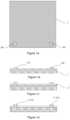
- FIG. 1 ais a top view and FIGS. 1 b , 1 c , and 1 d are sectional views illustrating a main manufacturing process of an on-chip type antenna according to a first embodiment of the present disclosure.
- FIGS. 2 a and 2 bare sectional views and FIG. 2 c is a top view illustrating the main manufacturing process of the on-chip type antenna according to the first embodiment of the present disclosure.
- FIGS. 3 a , 3 b , and 3 care sectional views and FIG. 3 d is a top view illustrating the main manufacturing process of the on-chip type antenna according to the first embodiment of the present disclosure.
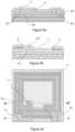
- FIGS. 4 a and 4 bare sectional views and FIG. 4 c is a top view illustrating the main manufacturing process of the on-chip type antenna according to the first embodiment of the present disclosure.
- FIGS. 5 a and 5 bare sectional views and FIG. 5 c is a top view illustrating the main manufacturing process of the on-chip type antenna according to the first embodiment of the present disclosure.
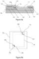
- FIG. 6 ais an enlarged top view of the on-chip type antenna according to the first embodiment of the present disclosure
- FIG. 6 bis an enlarged top view of an on-chip type antenna using a conventional wiring structure.
- FIG. 7 ais a sectional view illustrating a step coating shape of an insulating film in the on-chip type antenna according to the first embodiment of the present disclosure
- FIG. 7 bis a sectional view illustrating a step coating shape of an insulating film in the on-chip type antenna using the conventional wiring structure.
- FIGS. 8 a to 8 eare sectional views illustrating a main manufacturing process of an on-chip type antenna according to a second embodiment of the present disclosure.
- FIG. 9 ais a sectional view and FIG. 9 b is a top view illustrating the main manufacturing process of the on-chip type antenna according to the second embodiment of the present disclosure.
- FIGS. 1 a and 1 billustrate a top view and a sectional view of an IC chip 1 in the wafer process, and electrodes 2 (a first electrode 2 a and a second electrode 2 b ) electrically connected to a circuit are formed on corner portions of an outer peripheral portion of the IC chip 1 on an insulating film (for example, a silicon nitride film, a resin film, or the like that is a passivation film) formed on an upper surface of the IC chip 1 of a contactless information carrier (an RFID tag).
- an insulating filmfor example, a silicon nitride film, a resin film, or the like that is a passivation film
- the IC chip 1is in a shape of, for example, a rectangle (including a square) with sides each having a length of 0.5 mm to 1 mm, but the shape thereof is not limited thereto.
- the arrangement of the first electrode 2 a and the second electrode 2 bis not limited to the positional relationship illustrated in the drawings, and the first electrode 2 a and the second electrode 2 b may be arranged on outer peripheral portions of different sides of the IC chip 1 , for example.
- IC chip 1is illustrated on a wafer in the figures, a plurality of IC chips 1 are certainly formed in alignment on one wafer in the wafer process.
- the electrodes 2are formed by a known wafer process technique, in which a film of metal such as copper, aluminum, or the like is formed by a vapor deposition method, a sputtering method, a plating method, or the like, so as to be patterned by a photolithography method and an etching method.
- the electrodes 2are connected to an electronic circuit of the IC chip 1 via unillustrated connecting holes.
- the IC chip 1is provided with electronic circuits (a memory, a memory control unit, a transmission unit, a power supply unit, and the like) necessary for a contactless information carrier, such as the electronic circuits described in Patent Literature 1, for example, the electronic circuits are not limited thereto. In the following drawings, the electronic circuits are omitted for the sake of simplicity.
- the electrodes 2may be bumps.
- a rotary coating filmis formed on the IC chip 1 .
- a first insulating film 3for example, a resin film of polyimide or the like, or a silicon oxide film
- the film thickness of the rotary coating film obtained at the endis, for example, 2 ⁇ m to 10 ⁇ m.
- a pattern of a photoresistis formed by using a lithography method, and then the first insulating film 3 is selectively etched by an etching method, leaving the necessary pattern.
- openings (connecting holes) 4are formed on the electrodes 2 by eliminating the photoresist. Specifically, a first opening 4 a and a second opening 4 b are formed on the first electrode 2 a and the second electrode 2 b , respectively.
- a photosensitive resin(a positive type or a negative type) of photosensitive polyimide or the like may be formed, exposed by a photolithography method, and selectively etched (developed) with an etching solution to form the openings (connecting holes or via holes) 4 .
- the first conductive film 5is also formed in the openings (connecting holes) 4 .
- the first conductive film 5is etched by wet etching or dry etching using the photoresist as a mask, and then the photoresist is eliminated so that the first conductive film 5 is patterned to form a first lower layer wiring 5 a and a second lower layer wiring 5 b.
- FIG. 2 cis a top view of the IC chip 1 on which the first lower layer wiring 5 a and the second lower layer wiring 5 b are formed. As illustrated in FIGS. 2 b and 2 c , the first lower layer wiring 5 a and the second lower layer wiring 5 b are electrically connected to the first electrode 2 a and the second electrode 2 b via the first opening 4 a and the second opening 4 b , respectively.
- a second insulating film 6(for example, a resin film of polyimide or the like, or a silicon oxide film) having a film thickness of 2 ⁇ m to 10 ⁇ m, for example, is formed by a rotary coating method or the like.
- openings (connecting holes) 7are formed, and more specifically, a third opening 7 a and a fourth opening 7 b are formed on the first lower layer wiring 5 a and the second lower layer wiring 5 b , respectively.
- a photosensitive resinmay be used as the second insulating film 6 to form the openings (connecting holes) 7 by a photolithography method.
- FIG. 3 dis a top view of the IC chip 1 in the present step
- FIGS. 3 b and 3 care sectional views taken along the lines A-A′ and B-B′ of FIG. 3 d , respectively.
- a second conductive film 8 of copper, aluminum, or the likefor example, having a film thickness of 2 ⁇ m to 10 ⁇ m, for example, is formed by a vapor deposition method, a sputtering method, a plating method, or the like.
- the second conductive film 8is patterned by a combination of a photolithography method and an etching method to form an antenna wiring (spiral wiring) 9 that is an upper layer wiring.
- the antenna wiring 9is arranged such that the first electrode 2 a and the second electrode 2 b are positioned on an outer peripheral side of the antenna wiring 9 .
- FIG. 4 cis a top view in the present step.
- the antenna wiring 9is a spiral wiring having a winding (spiral) shape with a line width of, for example, 7 ⁇ m to 15 ⁇ m, has a line spacing (space width) of, for example, 7 ⁇ m to 15 ⁇ m, and is wound a plurality of times, for example, 2 to 10 times.
- the IC chip 1has a region in which the antenna wiring 9 is not formed in the central portion thereof.
- the antenna wiring 9has a first end portion 10 a and a second end portion 10 b , which cover the third opening 7 a and the fourth opening 7 b and are positioned on an inner peripheral side and the outer peripheral side of the antenna wiring 9 in a spiral shape (spiral wiring), respectively.
- the first end portion 10 a and the second end portion 10 bare electrically connected to the first lower layer wiring 5 a and the second lower layer wiring 5 b in (via) the third opening 7 a and the fourth opening 7 b , respectively.
- the first end portion 10 ais electrically connected to the first electrode 2 a via the third opening 7 a (inner peripheral side connecting hole) positioned on the inner peripheral side, the first lower layer wiring 5 a , and the first opening 4 a (outer peripheral side connecting hole) positioned on the outer peripheral side.
- the first lower layer wiring 5 ais a relay wiring (a first relay wiring) for electrically relaying the first end portion 10 a positioned on the inner peripheral side to the first electrode 2 a positioned on the outer peripheral side.
- the second end portion 10 bis electrically connected to the second electrode 2 b via the second lower layer wiring 5 b
- the second lower layer wiring 5 bis a relay wiring (a second relay wiring) for electrically relaying the second end portion 10 b to the second electrode 2 b.
- the second end portion 10 bmay be connected to the second electrode 2 b without passing via (using) the second lower layer wiring 5 b .
- the second opening 4 b and the fourth opening 7 bmay be aligned with each other on the second electrode 2 a to directly connect the second end portion 10 b to the second electrode 2 b via the second opening 4 b and the fourth opening 7 b .
- a conductive plugmay be embedded in both the openings (connecting holes) so that both the openings are overlapped with each other in the vertical direction.
- a third insulating film 11for example, a resin film or the like of polyimide or the like is formed, as a protective film for protecting the antenna wiring 9 , by a coating method or the like.
- FIG. 5 cillustrates a top view of the IC chip 1 in the present step
- FIG. 5 a and FIG. 5 billustrate cross sections taken along the lines A-A′ and B-B′ of FIG. 5 c , respectively.
- FIG. 6 ais an enlarged view of a region C illustrated by the alternate long and short dash line in FIG. 4 c.
- the first lower layer wiring 5 ais formed in such a manner as to include a region of a virtual rectangle R having, at the apexes of the diagonal line, the first opening 4 a formed at the upper part of the first electrode 2 a and the third opening 7 a formed at the lower part of the first end portion 10 a of the antenna wiring 9 .
- the first lower layer wiring 5 ahas, for example, a rectangular shape. Note that, strictly speaking, the first opening 4 a and the third opening 7 a are not points because they each have a finite size, but the rectangle can be defined as the smallest rectangle including the first opening 4 a and the third opening 7 a arranged diagonally.
- FIG. 6 billustrates a top view of the IC chip when a line-shaped wiring 51 is used instead of the first lower layer wiring 5 a as the lower layer wiring.
- the width of the line-shaped wiring 51is approximately the same as the line width of the antenna wiring 9 .
- the first opening 4 ais positioned on the outer peripheral side of the antenna wiring 9
- the third opening 7 ais positioned on the inner peripheral side of the antenna wiring 9
- the virtual rectangle R including the first opening 4 a and the third opening 7 ais a rectangle in which a length of one side is equal to a maximum distance Dx in the X-axis direction including the first opening 4 a and the third opening 7 a , and a length of the other side is equal to a maximum distance Dy in the Y-axis direction including the first opening 4 a and the third opening 7 a
- the first lower layer wiring 5 ahas a shape including this rectangle R.
- the first lower layer wiring 5 acan be a rectangle having a side Sx with a length Lx in the X-axis direction and a side Sy with a length Ly in the Y-axis direction in FIG. 6 a , wherein Lx ⁇ Dx and Ly ⁇ Dy.
- a plurality of antenna wirings 9intersect in different directions (the Y-axis direction and the X-axis direction), respectively, on the two sides intersecting each other having the lengths Lx and Ly.
- Zx and Zyare, for example, 30 ⁇ m to 90 ⁇ m, but are not limited thereto.
- the first lower layer wiring 5 afunctions as a wiring for electrically connecting the first electrode 2 a and the first end portion 10 a .
- an electric currentflows two-dimensionally, which may reduce electrical resistance between the first electrode 2 a and the first end portion 10 a.
- FIG. 7 ais an enlarged view of a cross section taken along the line A-A′ of FIG. 6 a
- FIG. 7 bis an enlarged view of a cross section taken along the line B-B′ of FIG. 6 b , illustrating a state of the step covering property (coverage) of an insulating film when the insulating film is formed by a rotary coating method.
- FIG. 7 billustrates an example in which the lower layer wiring is patterned in the shape of the normal wiring 51 as disclosed in Patent Literature 3.
- the second insulating film 6 (of the rotary coating film) formed by the rotary coating methodis in contact with corner portions of the wiring 51 .
- the film thickness of the second insulating film 6is thin.
- the wiring 51 that is the lower layer wiring and the antenna wiring 9 that is the upper layer wiringare short-circuited, which may reduce product yield.
- a width of the wiring 51(a line width L) is equal to or less than a film thickness of the second insulating film 6 to be formed, the above risk may be significant.
- the radius of curvature of regions Q and Q′ of the antenna wiring 9 on the corner portions of the wiring 51is small, there is a possibility that the antenna wiring 9 is cracked and disconnected by stresses from the second insulating film 6 and the third insulating film 11 , which may reduce product yield.
- the stresses of the second insulating film 6 and the third insulating film 11act substantially symmetrically so that the stresses strengthen each other (the stresses are combined in the same direction), which increases a risk of the antenna wiring 9 being cracked.
- the covering property at a step portion of the second conductive film 8may be deteriorated.
- the line width of the first lower layer wiring 5 ais wider than each of the intervals Zx and Zy of the antenna wiring 9 , and is, for example, 5 times wider or more, typically 30 times wider or more than the film thickness of the second insulating film 6 to be formed. Therefore, in the shape of the region P (the corner portion of the first lower layer wiring 5 a ) of the second insulating film 6 formed by a rotary coating method, the radius of curvature can be made large (smooth). For this reason, it is possible to inhibit the film thickness of the second insulating film 6 from being thinned.
- the structure of the first lower layer wiring 5 aallows the first lower layer wiring 5 a and the antenna wiring 9 to intersect at different positions and in different directions (see FIG. 6 a ). Therefore, unlike in FIG. 7 b , the stresses are not combined.
- the covering property at the step portion of the second conductive film 8is improved.
- the shape of the first lower layer wiring 5 a of the present disclosurealso allows, for example, a larger degree of freedom in antenna design as described below.
- L and Care an equivalent inductance and an equivalent capacitance of the antenna coil.
- the electric power induced by the radio wave from a reader/writerincreases substantially in proportion to the number of turns of the coil.
- designis made such that a large amount of electric power can be obtained by satisfying the value of the inductance L for achieving the above resonance frequency.
- the input impedance of the IC chip 1may vary depending on the circuit adopted for the IC chip 1 .
- the impedances of the IC chip 1 and the antenna wiring 9so as to transmit, to the IC chip 1 , the electric power obtained by the radio wave from the reader/writer, it is also possible to obtain a more preferred antenna coil.
- the inter-wiring space of the antenna wiring 9affects the inter-wiring capacitance of the antenna wiring 9 , it is difficult to independently control the inductance L and the capacitance C only by the antenna wiring 9 .
- the antenna wiring 9 and the first lower layer wiring 5 ato face each other, forming the first lower layer wiring 5 a in a rectangular shape, for example, and changing Lx and Ly, it is possible to adjust the capacitance C at least partially, and is also possible to control both the inductance L and the capacitance C independently.
- the antenna coilBy utilizing the special shape of the first lower layer wiring 5 a and structuring the antenna such that the inductance L and the capacitance C can be controlled, a larger degree of freedom is allowed in designing the antenna coil, which also makes it possible to easily obtain the optimum on-chip type coil.
- the inductance L of the coilis generally proportional to the square of the number of turns and to the sectional area of the coil.
- the IC chip 1is miniaturized and a sufficient inductance L cannot be obtained, it is possible to achieve the necessary resonance frequency by increasing the capacitance C so that the value of the product of LC in the above equation of the resonance frequency is increased.
- the step covering property of the second insulating film ( 6 ) on the first relay wiring ( 5 a )is improved, and a spiral wiring having good electrical characteristics can be obtained. Then, it is possible to provide a contactless information medium (for example, an RFID tag) provided with an on-chip type antenna capable of achieving both miniaturization and good electrical characteristics.
- a contactless information mediumfor example, an RFID tag
- a conductive film (a metal film) of the wiringis wet-etched using a pattern of a photoresist as a mask to form the wiring pattern (lower layer wiring, antenna wiring)
- a side wall of the wiring pattern after etchingis etched and the etching amount increases toward the upper part of the wiring because the wet etching is isotropic etching.
- the thicker the film thickness of the conductive film of the wiringis, the more difficult it is to control the sectional shape of the wiring.
- wiring resistance and the variation thereofmay increase.
- the patterning of the wiring capable of controlling the sectional shape of the wiringwill be described mainly by taking the lower layer wirings 5 a and 5 b as examples, but the same applies to the patterning of the antenna wiring 9 .
- a conductive seed layer 12for example, of Ni, Cr, Ti, Ta, or TiW, or a laminated film having copper (Cu) on the film of such a metal, with a total film thickness of 0.03 ⁇ m to 0.5 ⁇ m, for example, is formed by a vapor deposition method, a sputtering method, or the like.
- a photosensitive insulating film 13(for example, of photosensitive polyimide, photoresist, or the like) is formed by a coating method.
- the plating seed layer 12functions as an electrode for feeding electric power when copper is formed by electrolytic plating.
- a metal nitride filmsuch as of TaN or TiN (or using it at least as a part of the laminated film), for example, it is also possible to obtain an effect of preventing the copper from diffusing into the insulating film.
- a metal film 14(for example, copper film) is selectively formed only on the exposed seed layer 12 by electrolytic plating using the seed layer 12 as an electrode.
- the mask pattern 13 a made of the photosensitive insulating film 13is eliminated.
- the metal film 14is formed on a part of the seed layer 12 as a reverse pattern of the mask pattern 13 a.
- the seed layer 12 not covered by the metal film 14is selectively etched using the metal film 14 as an etching mask, leaving only the seed layer 12 under the metal film 14 .
- dissimilar metalsmay come into contact with each other.
- the second insulating film 6is formed.
- the lower layer wirings(the first lower layer wiring 5 a and the second lower layer wiring 5 b ) having the laminated structure of the metal film 14 and the seed layer 12 can be formed.
- the negative type photosensitive insulating layer 13can be suitably used.
- the antenna wiring 9(including the first end portion 10 a and the second end portion 10 b ) having a laminated structure of a metal film 14 ′ and a seed layer 12 ′ can be formed.
- the sectional shape of the wiringsare determined by the mask pattern 13 a of the photosensitive insulating layer 13 , and the shape of the mask pattern 13 a of the photosensitive insulating layer 13 is optically determined by a photolithography method. For this reason, the sectional shape of the formed wiring has a side wall surface that rises steeply as compared with the sectional shape of the wiring formed by using wet etching that is isotropic etching.
- the wiring formed by the above methodhas the laminated structure of the metal film 14 ( 14 ′) and the seed layer 12 ( 12 ′).
- a seed layer 12 ′is interposed at the bottom portion of the third opening (connecting hole) 7 a where the antenna wiring 9 comes into contact with the first lower layer wiring 5 a at the first end portion 10 a .
- contact resistancemay increase (due to the formation of an alloy layer or the like).
- the structure of the first lower layer wiring 5 acan effectively reduce the contact resistance.
- FIG. 9 bis a diagram schematically illustrating mutual positional relationships between the first lower layer wiring 5 a , and the first opening 4 a and the third opening (connecting hole) 7 a , and corresponds to the region C of FIG. 4 c.
- the first lower layer wiring 5 ahas a shape including the virtual rectangle R having the first opening (connecting hole) 4 a and the third opening (connecting hole) 7 a as the apexes of the diagonal line.
- the current path between the rectangle R and the third opening (connecting hole) 7 aincludes at least sides S 1 and S 2 .
- the peripheral portion via which the electric current flowsis limited in one direction due to the width of the wiring 51 , resulting in increase in the resistance.
- the path via which the electric current flows toward the third opening (connecting hole) 7 acan be increased, and the contact resistance can be reduced.
- the contact resistancecan be similarly reduced.
- the IC chip 1 provided with the above antenna wiring 9can be packaged after a known dicing step, which can provide a contactless information carrier such as an RFID tag, for example.
- the electrically good on-chip type antennacan be achieved, and the contactless information carrier capable of being used for an RFID tag and the like can be provided, which makes the industrial applicability thereof significant.
- FIGS. 1 - 9show example configurations with relative positioning of the various components. If shown directly contacting each other, or directly coupled, then such elements may be referred to as directly contacting or directly coupled, respectively, at least in one example. Similarly, elements shown contiguous or adjacent to one another may be contiguous or adjacent to each other, respectively, at least in one example. As an example, components laying in face-sharing contact with each other may be referred to as in face-sharing contact. As another example, elements positioned apart from each other with only a space there-between and no other components may be referred to as such, in at least one example.
- top/bottom, upper/lower, above/belowmay be relative to a vertical axis of the figures and used to describe positioning of elements of the figures relative to one another.
- elements shown above other elementsare positioned vertically above the other elements, in one example.
- shapes of the elements depicted within the figuresmay be referred to as having those shapes (e.g., such as being circular, straight, planar, curved, rounded, chamfered, angled, or the like).
- elements shown intersecting one anothermay be referred to as intersecting elements or intersecting one another, in at least one example.
- an element shown within another element or shown outside of another elementmay be referred as such, in one example.
Landscapes
- Engineering & Computer Science (AREA)
- Microelectronics & Electronic Packaging (AREA)
- Computer Hardware Design (AREA)
- Physics & Mathematics (AREA)
- General Physics & Mathematics (AREA)
- Theoretical Computer Science (AREA)
- Computer Networks & Wireless Communication (AREA)
- Internal Circuitry In Semiconductor Integrated Circuit Devices (AREA)
- Details Of Aerials (AREA)
- Variable-Direction Aerials And Aerial Arrays (AREA)
- Semiconductor Integrated Circuits (AREA)
Abstract
Description
- Patent Literature 1: Japanese Patent Laid-Open No. 04-167719
- Patent Literature 2: Japanese Patent No. 6251770
- Patent Literature 3: Japanese Patent Laid-Open No. 2002-92568
- Patent Literature 4: Japanese Patent Laid-Open No. 2001-351082
- a spiral wiring (9) having a first end portion (10a) and a second end portion (10b) electrically connected to the first electrode (2a) and the second electrode (2b), respectively, in which
- the IC chip (1) is provided with
- a first insulating film (3) on the first electrode (2a) and the second electrode (2b),
- a first relay wiring (5a) on the first insulating film (3), and
- a second insulating film (6) on the first relay wiring (5a),
- the spiral wiring (9) is formed on the second insulating film (6),
- the first end portion (10a) and the second end portion (10b) are positioned on an inner peripheral side and an outer peripheral side of the spiral wiring (9), respectively,
- the first electrode (2a) and the second electrode (2b) are positioned on the outer peripheral side of the spiral wiring (9), and
- the first relay wiring (5a)
- is connected to the first electrode (2a) via a first connecting hole (4a) formed in the first insulating film (3) and is connected to the first end portion (10a) via a third connecting hole (7a) formed in the second insulating film (6), and
- includes a rectangular region diagonally including the first connecting hole (4a) and the third connecting hole (7a).
f=½π×√(LC)
- 1 IC chip
- 2 Electrodes
- 2aFirst electrode
- 2bSecond electrode
- 3 First insulating film
- 4 Openings (connecting holes)
- 4aFirst opening (connecting hole)
- 4bSecond opening (connecting hole)
- 5 First conductive film
- 5aFirst lower layer wiring
- 5bSecond lower layer wiring
- 6 Second insulating film
- 7 Openings (connecting holes)
- 7aThird opening (connecting hole)
- 7bFourth opening (connecting hole)
- 8 Second conductive film
- 9 Antenna wiring (spiral wiring)
- 10aFirst end portion
- 10bSecond end portion
- 11 Third insulating film
- 12,12′ Seed layer
- 13 Photosensitive insulating film
- 13aMask pattern
- 14,14′ Metal film
- 51 Wiring
Claims (4)
Applications Claiming Priority (3)
| Application Number | Priority Date | Filing Date | Title |
|---|---|---|---|
| JP2019-075071 | 2019-04-10 | ||
| JP2019075071AJP6546711B1 (en) | 2019-04-10 | 2019-04-10 | Non-contact information carrier |
| PCT/JP2020/015714WO2020209261A1 (en) | 2019-04-10 | 2020-04-07 | Contactless information carrier |
Publications (2)
| Publication Number | Publication Date |
|---|---|
| US20220172019A1 US20220172019A1 (en) | 2022-06-02 |
| US12236306B2true US12236306B2 (en) | 2025-02-25 |
Family
ID=67297600
Family Applications (1)
| Application Number | Title | Priority Date | Filing Date |
|---|---|---|---|
| US17/594,302Active2041-04-04US12236306B2 (en) | 2019-04-10 | 2020-04-07 | Contactless information carrier |
Country Status (6)
| Country | Link |
|---|---|
| US (1) | US12236306B2 (en) |
| EP (1) | EP3955375B1 (en) |
| JP (1) | JP6546711B1 (en) |
| CN (1) | CN113994539B (en) |
| TW (1) | TWI718045B (en) |
| WO (1) | WO2020209261A1 (en) |
Citations (72)
| Publication number | Priority date | Publication date | Assignee | Title |
|---|---|---|---|---|
| JPH04167719A (en) | 1990-10-30 | 1992-06-15 | Omron Corp | Data carrier |
| US20010027009A1 (en)* | 2000-02-22 | 2001-10-04 | Naoteru Matsubara | Method of fabricating semiconductor device |
| US20010044013A1 (en)* | 1994-03-04 | 2001-11-22 | Mcdonough Neil | Thin film transferrable electric components |
| JP2001351082A (en)* | 2000-06-08 | 2001-12-21 | Dainippon Printing Co Ltd | Non-contact IC chip, non-contact IC module and non-contact IC information processing medium |
| JP2002092568A (en) | 2000-09-14 | 2002-03-29 | Dainippon Printing Co Ltd | Coil-on-chip module, method for manufacturing the same, and non-contact type IC card |
| US6404644B1 (en) | 1997-07-10 | 2002-06-11 | Rohm Co., Ltd. | Non-contact IC card |
| US6424315B1 (en)* | 2000-08-02 | 2002-07-23 | Amkor Technology, Inc. | Semiconductor chip having a radio-frequency identification transceiver |
| US20020160786A1 (en)* | 2001-04-30 | 2002-10-31 | Manfred Rietzler | Selective metal removal process for metallized retro-reflective and holographic films and radio frequency devices made therewith |
| US20030085454A1 (en)* | 2001-10-12 | 2003-05-08 | Ulrich Reutner | Chip card and production process |
| JP2004280627A (en) | 2003-03-18 | 2004-10-07 | Hitachi Maxell Ltd | Semiconductor device |
| US20050046573A1 (en)* | 2001-04-30 | 2005-03-03 | Velasco Francisco Martinez De | Selective metal removal process for metallized retro-reflective and holographic films and radio frequency devices made therewith |
| US6867983B2 (en)* | 2002-08-07 | 2005-03-15 | Avery Dennison Corporation | Radio frequency identification device and method |
| US20060143898A1 (en)* | 2004-12-28 | 2006-07-06 | Samsung Techwin Co., Ltd. | Method of manufacturing antenna for RFID tag |
| US20070187820A1 (en)* | 2006-02-10 | 2007-08-16 | Semiconductor Energy Laboratory Co., Ltd. | Semiconductor device |
| CN101189625A (en) | 2005-05-31 | 2008-05-28 | 株式会社半导体能源研究所 | Semiconductor device, manufacturing method thereof, and antenna manufacturing method |
| US20090146790A1 (en)* | 2006-07-24 | 2009-06-11 | Francisco Speich | RFID tag and method and device for the production thereof |
| US20090160719A1 (en)* | 2007-12-20 | 2009-06-25 | Murata Manufacturing Co., Ltd. | Radio frequency ic device |
| US7605706B2 (en)* | 2005-05-13 | 2009-10-20 | The Kennedy Group, Inc. | Patch antenna for RFID tag |
| US20090289797A1 (en)* | 2008-05-26 | 2009-11-26 | Isao Sakama | Rfid tag for structure |
| US20100001079A1 (en)* | 2008-02-27 | 2010-01-07 | Tagsys Sas | Combined EAS/RFID tag |
| US7667329B2 (en) | 2005-11-21 | 2010-02-23 | Stmicroelectronics Sa | Electronic micromodule and method for manufacturing the same |
| US7808030B2 (en)* | 2005-11-25 | 2010-10-05 | Fujitsu Limited | Electronic component manufacturing method and electronic component |
| US20110024510A1 (en)* | 2008-05-22 | 2011-02-03 | Murata Manufacturing Co., Ltd. | Wireless ic device |
| US20110063184A1 (en)* | 2006-12-28 | 2011-03-17 | Yuji Furumura | Base sheet |
| US20110073661A1 (en)* | 2009-09-25 | 2011-03-31 | Avery Dennison Corporation | Method, system and apparatus for manufacturing a radio frequency identification device |
| US20110090058A1 (en)* | 2008-07-04 | 2011-04-21 | Murata Manufacturing Co., Ltd. | Radio ic device |
| US20110128195A1 (en)* | 2008-08-06 | 2011-06-02 | Byung Hoon Ryou | Embedded antenna of wireless device and method of manufacturing thereof |
| US20110266351A1 (en)* | 2008-11-03 | 2011-11-03 | Ksw Microtec Ag | Method for producing an rfid transponder product, and rfid transponder product produced using the method |
| US8136735B2 (en)* | 2004-01-23 | 2012-03-20 | Semiconductor Energy Laboratory Co., Ltd. | ID label, ID card, and ID tag |
| US20120091821A1 (en)* | 2009-04-21 | 2012-04-19 | Murata Manufacturing Co., Ltd. | Antenna apparatus |
| US20120326931A1 (en)* | 2010-03-03 | 2012-12-27 | Murata Manufacturing Co., Ltd. | Wireless communication module and wireless communication device |
| US20130002502A1 (en)* | 2010-03-19 | 2013-01-03 | Shanghai Ic R&D Center Co., Ltd. | Multi-system multi-band rfid antenna |
| US20130154885A1 (en)* | 2010-06-21 | 2013-06-20 | Leonhard Kurz Stiftung & Co. Kg | Multilayered film element |
| US20130186961A1 (en)* | 2011-02-28 | 2013-07-25 | Murata Manufacturing Co., Ltd. | Wireless communication device |
| US8676117B2 (en)* | 2006-01-19 | 2014-03-18 | Murata Manufacturing Co., Ltd. | Wireless IC device and component for wireless IC device |
| US20140124582A1 (en)* | 2012-11-02 | 2014-05-08 | Flextronics Ap, Llc | Embedded high frequency rfid |
| US20140198011A1 (en)* | 2012-05-28 | 2014-07-17 | Murata Manufacturing Co., Ltd. | Antenna device and wireless communication apparatus |
| US20140203976A1 (en)* | 2011-12-22 | 2014-07-24 | Murata Manufacturing Co., Ltd. | Magnetic antenna, antenna device, and electronic apparatus |
| US20140203991A1 (en)* | 2012-02-01 | 2014-07-24 | Murata Manufacturing Co., Ltd. | Antenna device and communication terminal device |
| US20140217183A1 (en)* | 2011-11-08 | 2014-08-07 | Murata Manufacturing Co., Ltd. | Antenna device and communication apparatus |
| US20140292611A1 (en)* | 2013-03-29 | 2014-10-02 | Murata Manufacturing Co., Ltd. | Antenna apparatus |
| US20140319230A1 (en)* | 2012-12-07 | 2014-10-30 | Murata Manufacturing Co., Ltd. | Antenna module |
| US20150035718A1 (en)* | 2012-08-09 | 2015-02-05 | Murata Manufacturing Co., Ltd. | Antenna device and wireless communication apparatus |
| US20150077296A1 (en)* | 2012-03-23 | 2015-03-19 | Lg Innotek Co., Ltd. | Antenna assembly and method for manufacturing same |
| US20150161502A1 (en)* | 2012-06-29 | 2015-06-11 | Beijing Basch Smartcard Co., Ltd. | Multilayer wiring type double-interface ic card antenna module |
| US20150171519A1 (en)* | 2012-05-31 | 2015-06-18 | Ls Cable & System Ltd. | Flexible printed circuit board for dual mode antennas, dual mode antenna and user device |
| WO2015182638A1 (en) | 2014-05-30 | 2015-12-03 | 株式会社村田製作所 | Antenna device and electronic device |
| US20150346039A1 (en)* | 2013-02-22 | 2015-12-03 | Murata Manufacturing Co., Ltd. | Sensor tag and manufacturing method for sensor tag |
| US20150356395A1 (en)* | 2012-07-13 | 2015-12-10 | Smartrac Ip B.V. | Transponder Layer and Method for Producing Same |
| US9436902B1 (en)* | 2008-03-11 | 2016-09-06 | Impinj, International Ltd. | RFID integrated circuits with large contact pads |
| US20160275391A1 (en)* | 2014-12-10 | 2016-09-22 | Texas Instruments Deutschland Gmbh | Miniature rfid tag with coil on ic package |
| US20170017868A1 (en)* | 2014-04-28 | 2017-01-19 | Murata Manufacturing Co., Ltd. | Wireless ic device, clip-shaped rfid tag, and article having rfid tag |
| US20170040107A1 (en)* | 2015-08-07 | 2017-02-09 | Nucurrent, Inc. | Method of providing a single structure multi mode antenna for wireless power transmission using magnetic field coupling |
| US20170040665A1 (en)* | 2015-08-06 | 2017-02-09 | Thin Film Electronics Asa | Wireless Communication Device with Integrated Ferrite Shield and Antenna, and Methods of Manufacturing the Same |
| US20170054213A1 (en)* | 2015-08-19 | 2017-02-23 | Nucurrent, Inc. | Multi-Mode Wireless Antenna Configurations |
| US9684864B1 (en)* | 2015-02-05 | 2017-06-20 | Flextronics Ap, Llc. | Method of making RFID antenna by placing wire on fabric |
| JP6251770B2 (en) | 2016-04-15 | 2017-12-20 | 株式会社エスケーエレクトロニクス | RFID tag |
| JP2018085730A (en) | 2017-11-27 | 2018-05-31 | 株式会社エスケーエレクトロニクス | RFID tag |
| US20180194158A1 (en)* | 2015-07-09 | 2018-07-12 | Assa Abloy Ab | Security document with transparent window |
| US20180216906A1 (en)* | 2017-02-01 | 2018-08-02 | Impact Resources, Inc. | Durable Asset Management Tag |
| US20180240005A1 (en)* | 2015-08-17 | 2018-08-23 | Smartrac Technology Gmbh | Transponder apparatus |
| US20180277954A1 (en)* | 2017-03-24 | 2018-09-27 | Samsung Electro-Mechanics Co., Ltd. | Antenna module |
| US20180277943A1 (en)* | 2015-01-27 | 2018-09-27 | At & S Austria Technologie & Systemtechnik Aktiengesellschaft | Component Carrier With Integrated Antenna Structure |
| US20180287258A1 (en)* | 2017-03-31 | 2018-10-04 | Samsung Electro-Mechanics Co., Ltd. | Antenna module and electronic device having the same |
| US20190000427A1 (en)* | 2015-12-22 | 2019-01-03 | TFM Inventions Limited | A skin patch |
| US20190012589A1 (en)* | 2017-07-09 | 2019-01-10 | Interlake Research, Llc | Tag assembly methods |
| US20190042907A1 (en)* | 2015-05-25 | 2019-02-07 | Gemalto Sa | Radio-frequency antenna circuit having interlocking mutual inductors |
| US10248902B1 (en)* | 2017-11-06 | 2019-04-02 | Féinics Amatech Teoranta | Coupling frames for RFID devices |
| US20190267698A1 (en)* | 2018-02-27 | 2019-08-29 | Thin Film Electronics Asa | Printed and/or thin film integrated circuit with integrated antenna, and methods of making and using the same |
| US20190294217A1 (en)* | 2018-03-23 | 2019-09-26 | Samsung Electro-Mechanics Co., Ltd. | Antenna module and electronic device including the same |
| US10886047B2 (en)* | 2013-11-25 | 2021-01-05 | A.K. Stamping Company, Inc. | Wireless charging coil |
| US11004599B2 (en)* | 2013-11-25 | 2021-05-11 | A.K. Stamping Company, Inc. | Wireless charging coil |
Family Cites Families (5)
| Publication number | Priority date | Publication date | Assignee | Title |
|---|---|---|---|---|
| JPS5455923A (en) | 1977-10-07 | 1979-05-04 | Nippon Denso Co Ltd | Method of and apparatus for safety control of vehicle at the time of travelling along curved road |
| TWI278084B (en)* | 2004-10-19 | 2007-04-01 | Advanced Semiconductor Eng | Chip scale package with micro antenna and method for manufacturing the same |
| US7839124B2 (en)* | 2006-09-29 | 2010-11-23 | Semiconductor Energy Laboratory Co., Ltd. | Wireless power storage device comprising battery, semiconductor device including battery, and method for operating the wireless power storage device |
| KR101611643B1 (en)* | 2008-10-01 | 2016-04-11 | 가부시키가이샤 한도오따이 에네루기 켄큐쇼 | Semiconductor device |
| TWI601229B (en)* | 2015-12-25 | 2017-10-01 | 韋僑科技股份有限公司 | Rfid device and method for making the same |
- 2019
- 2019-04-10JPJP2019075071Apatent/JP6546711B1/enactiveActive
- 2020
- 2020-04-07EPEP20786719.3Apatent/EP3955375B1/enactiveActive
- 2020-04-07WOPCT/JP2020/015714patent/WO2020209261A1/ennot_activeCeased
- 2020-04-07CNCN202080027776.6Apatent/CN113994539B/enactiveActive
- 2020-04-07USUS17/594,302patent/US12236306B2/enactiveActive
- 2020-04-10TWTW109112144Apatent/TWI718045B/enactive
Patent Citations (74)
| Publication number | Priority date | Publication date | Assignee | Title |
|---|---|---|---|---|
| JPH04167719A (en) | 1990-10-30 | 1992-06-15 | Omron Corp | Data carrier |
| US20010044013A1 (en)* | 1994-03-04 | 2001-11-22 | Mcdonough Neil | Thin film transferrable electric components |
| US6404644B1 (en) | 1997-07-10 | 2002-06-11 | Rohm Co., Ltd. | Non-contact IC card |
| US20010027009A1 (en)* | 2000-02-22 | 2001-10-04 | Naoteru Matsubara | Method of fabricating semiconductor device |
| JP2001351082A (en)* | 2000-06-08 | 2001-12-21 | Dainippon Printing Co Ltd | Non-contact IC chip, non-contact IC module and non-contact IC information processing medium |
| US6424315B1 (en)* | 2000-08-02 | 2002-07-23 | Amkor Technology, Inc. | Semiconductor chip having a radio-frequency identification transceiver |
| JP2002092568A (en) | 2000-09-14 | 2002-03-29 | Dainippon Printing Co Ltd | Coil-on-chip module, method for manufacturing the same, and non-contact type IC card |
| US20050046573A1 (en)* | 2001-04-30 | 2005-03-03 | Velasco Francisco Martinez De | Selective metal removal process for metallized retro-reflective and holographic films and radio frequency devices made therewith |
| US20020160786A1 (en)* | 2001-04-30 | 2002-10-31 | Manfred Rietzler | Selective metal removal process for metallized retro-reflective and holographic films and radio frequency devices made therewith |
| US20030085454A1 (en)* | 2001-10-12 | 2003-05-08 | Ulrich Reutner | Chip card and production process |
| US6867983B2 (en)* | 2002-08-07 | 2005-03-15 | Avery Dennison Corporation | Radio frequency identification device and method |
| JP2004280627A (en) | 2003-03-18 | 2004-10-07 | Hitachi Maxell Ltd | Semiconductor device |
| US8136735B2 (en)* | 2004-01-23 | 2012-03-20 | Semiconductor Energy Laboratory Co., Ltd. | ID label, ID card, and ID tag |
| US20060143898A1 (en)* | 2004-12-28 | 2006-07-06 | Samsung Techwin Co., Ltd. | Method of manufacturing antenna for RFID tag |
| US7605706B2 (en)* | 2005-05-13 | 2009-10-20 | The Kennedy Group, Inc. | Patch antenna for RFID tag |
| CN101189625A (en) | 2005-05-31 | 2008-05-28 | 株式会社半导体能源研究所 | Semiconductor device, manufacturing method thereof, and antenna manufacturing method |
| US7667329B2 (en) | 2005-11-21 | 2010-02-23 | Stmicroelectronics Sa | Electronic micromodule and method for manufacturing the same |
| US7808030B2 (en)* | 2005-11-25 | 2010-10-05 | Fujitsu Limited | Electronic component manufacturing method and electronic component |
| US8676117B2 (en)* | 2006-01-19 | 2014-03-18 | Murata Manufacturing Co., Ltd. | Wireless IC device and component for wireless IC device |
| US20070187820A1 (en)* | 2006-02-10 | 2007-08-16 | Semiconductor Energy Laboratory Co., Ltd. | Semiconductor device |
| US20090146790A1 (en)* | 2006-07-24 | 2009-06-11 | Francisco Speich | RFID tag and method and device for the production thereof |
| US20110063184A1 (en)* | 2006-12-28 | 2011-03-17 | Yuji Furumura | Base sheet |
| US20090160719A1 (en)* | 2007-12-20 | 2009-06-25 | Murata Manufacturing Co., Ltd. | Radio frequency ic device |
| US20100001079A1 (en)* | 2008-02-27 | 2010-01-07 | Tagsys Sas | Combined EAS/RFID tag |
| US9436902B1 (en)* | 2008-03-11 | 2016-09-06 | Impinj, International Ltd. | RFID integrated circuits with large contact pads |
| US20110024510A1 (en)* | 2008-05-22 | 2011-02-03 | Murata Manufacturing Co., Ltd. | Wireless ic device |
| US20090289797A1 (en)* | 2008-05-26 | 2009-11-26 | Isao Sakama | Rfid tag for structure |
| US20110090058A1 (en)* | 2008-07-04 | 2011-04-21 | Murata Manufacturing Co., Ltd. | Radio ic device |
| US20110128195A1 (en)* | 2008-08-06 | 2011-06-02 | Byung Hoon Ryou | Embedded antenna of wireless device and method of manufacturing thereof |
| US20110266351A1 (en)* | 2008-11-03 | 2011-11-03 | Ksw Microtec Ag | Method for producing an rfid transponder product, and rfid transponder product produced using the method |
| US20120091821A1 (en)* | 2009-04-21 | 2012-04-19 | Murata Manufacturing Co., Ltd. | Antenna apparatus |
| US20110073661A1 (en)* | 2009-09-25 | 2011-03-31 | Avery Dennison Corporation | Method, system and apparatus for manufacturing a radio frequency identification device |
| US20120326931A1 (en)* | 2010-03-03 | 2012-12-27 | Murata Manufacturing Co., Ltd. | Wireless communication module and wireless communication device |
| US20130002502A1 (en)* | 2010-03-19 | 2013-01-03 | Shanghai Ic R&D Center Co., Ltd. | Multi-system multi-band rfid antenna |
| US20130154885A1 (en)* | 2010-06-21 | 2013-06-20 | Leonhard Kurz Stiftung & Co. Kg | Multilayered film element |
| US20130186961A1 (en)* | 2011-02-28 | 2013-07-25 | Murata Manufacturing Co., Ltd. | Wireless communication device |
| US20140217183A1 (en)* | 2011-11-08 | 2014-08-07 | Murata Manufacturing Co., Ltd. | Antenna device and communication apparatus |
| US20140203976A1 (en)* | 2011-12-22 | 2014-07-24 | Murata Manufacturing Co., Ltd. | Magnetic antenna, antenna device, and electronic apparatus |
| US20140203991A1 (en)* | 2012-02-01 | 2014-07-24 | Murata Manufacturing Co., Ltd. | Antenna device and communication terminal device |
| US20150077296A1 (en)* | 2012-03-23 | 2015-03-19 | Lg Innotek Co., Ltd. | Antenna assembly and method for manufacturing same |
| US20140198011A1 (en)* | 2012-05-28 | 2014-07-17 | Murata Manufacturing Co., Ltd. | Antenna device and wireless communication apparatus |
| US20150171519A1 (en)* | 2012-05-31 | 2015-06-18 | Ls Cable & System Ltd. | Flexible printed circuit board for dual mode antennas, dual mode antenna and user device |
| US20150161502A1 (en)* | 2012-06-29 | 2015-06-11 | Beijing Basch Smartcard Co., Ltd. | Multilayer wiring type double-interface ic card antenna module |
| US20150356395A1 (en)* | 2012-07-13 | 2015-12-10 | Smartrac Ip B.V. | Transponder Layer and Method for Producing Same |
| US20150035718A1 (en)* | 2012-08-09 | 2015-02-05 | Murata Manufacturing Co., Ltd. | Antenna device and wireless communication apparatus |
| US20140124582A1 (en)* | 2012-11-02 | 2014-05-08 | Flextronics Ap, Llc | Embedded high frequency rfid |
| US20140319230A1 (en)* | 2012-12-07 | 2014-10-30 | Murata Manufacturing Co., Ltd. | Antenna module |
| US20150346039A1 (en)* | 2013-02-22 | 2015-12-03 | Murata Manufacturing Co., Ltd. | Sensor tag and manufacturing method for sensor tag |
| US20140292611A1 (en)* | 2013-03-29 | 2014-10-02 | Murata Manufacturing Co., Ltd. | Antenna apparatus |
| US11004599B2 (en)* | 2013-11-25 | 2021-05-11 | A.K. Stamping Company, Inc. | Wireless charging coil |
| US10886047B2 (en)* | 2013-11-25 | 2021-01-05 | A.K. Stamping Company, Inc. | Wireless charging coil |
| US20170017868A1 (en)* | 2014-04-28 | 2017-01-19 | Murata Manufacturing Co., Ltd. | Wireless ic device, clip-shaped rfid tag, and article having rfid tag |
| WO2015182638A1 (en) | 2014-05-30 | 2015-12-03 | 株式会社村田製作所 | Antenna device and electronic device |
| US20170194711A1 (en)* | 2014-05-30 | 2017-07-06 | Murata Manufacturing Co., Ltd. | Antenna device and electronic apparatus |
| US20160275391A1 (en)* | 2014-12-10 | 2016-09-22 | Texas Instruments Deutschland Gmbh | Miniature rfid tag with coil on ic package |
| US20180277943A1 (en)* | 2015-01-27 | 2018-09-27 | At & S Austria Technologie & Systemtechnik Aktiengesellschaft | Component Carrier With Integrated Antenna Structure |
| US9684864B1 (en)* | 2015-02-05 | 2017-06-20 | Flextronics Ap, Llc. | Method of making RFID antenna by placing wire on fabric |
| US20190042907A1 (en)* | 2015-05-25 | 2019-02-07 | Gemalto Sa | Radio-frequency antenna circuit having interlocking mutual inductors |
| US20180194158A1 (en)* | 2015-07-09 | 2018-07-12 | Assa Abloy Ab | Security document with transparent window |
| US20170040665A1 (en)* | 2015-08-06 | 2017-02-09 | Thin Film Electronics Asa | Wireless Communication Device with Integrated Ferrite Shield and Antenna, and Methods of Manufacturing the Same |
| US20170040107A1 (en)* | 2015-08-07 | 2017-02-09 | Nucurrent, Inc. | Method of providing a single structure multi mode antenna for wireless power transmission using magnetic field coupling |
| US20180240005A1 (en)* | 2015-08-17 | 2018-08-23 | Smartrac Technology Gmbh | Transponder apparatus |
| US20170054213A1 (en)* | 2015-08-19 | 2017-02-23 | Nucurrent, Inc. | Multi-Mode Wireless Antenna Configurations |
| US20190000427A1 (en)* | 2015-12-22 | 2019-01-03 | TFM Inventions Limited | A skin patch |
| US20190080215A1 (en)* | 2016-04-15 | 2019-03-14 | Sk-Electronics Co., Ltd. | RFID Tag |
| JP6251770B2 (en) | 2016-04-15 | 2017-12-20 | 株式会社エスケーエレクトロニクス | RFID tag |
| US20180216906A1 (en)* | 2017-02-01 | 2018-08-02 | Impact Resources, Inc. | Durable Asset Management Tag |
| US20180277954A1 (en)* | 2017-03-24 | 2018-09-27 | Samsung Electro-Mechanics Co., Ltd. | Antenna module |
| US20180287258A1 (en)* | 2017-03-31 | 2018-10-04 | Samsung Electro-Mechanics Co., Ltd. | Antenna module and electronic device having the same |
| US20190012589A1 (en)* | 2017-07-09 | 2019-01-10 | Interlake Research, Llc | Tag assembly methods |
| US10248902B1 (en)* | 2017-11-06 | 2019-04-02 | Féinics Amatech Teoranta | Coupling frames for RFID devices |
| JP2018085730A (en) | 2017-11-27 | 2018-05-31 | 株式会社エスケーエレクトロニクス | RFID tag |
| US20190267698A1 (en)* | 2018-02-27 | 2019-08-29 | Thin Film Electronics Asa | Printed and/or thin film integrated circuit with integrated antenna, and methods of making and using the same |
| US20190294217A1 (en)* | 2018-03-23 | 2019-09-26 | Samsung Electro-Mechanics Co., Ltd. | Antenna module and electronic device including the same |
Non-Patent Citations (5)
| Title |
|---|
| European Patent Office, Extended European Search Report Issued in Application No. 20786719.3, Nov. 16, 2022, Germany, 8 pages. |
| ISA Japan Patent Office, International Search Report Issued in Application No. PCT/JP2020/015714, Jul. 7, 2020, WIPO, 4 pages. |
| Japanese Patent Office, Office Action Issued in Application No. 2019-075071, May 28, 2022, 6 pages. |
| State Intellectual Property Office of the People's Republic of China, Office Action and Search Report Issued in Application No. 202080027776.6, Apr. 6, 2022, 12 pages. (Submitted with Partial Translation). |
| United States Patent and Trademark Office, Certificate of Correction Issued in U.S. Appl. No. 11/561,699, U.S. Pat. No. 7,667,329B2, filed Feb. 23, 2010, 1 page. |
Also Published As
| Publication number | Publication date |
|---|---|
| CN113994539B (en) | 2022-12-20 |
| CN113994539A (en) | 2022-01-28 |
| JP6546711B1 (en) | 2019-07-17 |
| JP2020174283A (en) | 2020-10-22 |
| EP3955375B1 (en) | 2024-09-25 |
| EP3955375A4 (en) | 2022-12-14 |
| WO2020209261A1 (en) | 2020-10-15 |
| TW202044514A (en) | 2020-12-01 |
| EP3955375A1 (en) | 2022-02-16 |
| TWI718045B (en) | 2021-02-01 |
| US20220172019A1 (en) | 2022-06-02 |
Similar Documents
| Publication | Publication Date | Title |
|---|---|---|
| US10013650B2 (en) | Wireless communication module and wireless communication device | |
| US7967216B2 (en) | Wireless IC device | |
| JP4544181B2 (en) | Electronic substrate, semiconductor device and electronic equipment | |
| US8259459B2 (en) | Electronic device | |
| US20200210803A1 (en) | Card-type wireless communication device | |
| US7312528B2 (en) | Semiconductor device having antenna connection electrodes | |
| JP5403145B2 (en) | Wireless communication device and wireless communication terminal | |
| EP3306533B1 (en) | Non-contact type information medium | |
| US12236306B2 (en) | Contactless information carrier | |
| JP5637004B2 (en) | Semiconductor integrated circuit module, wireless communication module, and wireless communication device | |
| JP4367070B2 (en) | Semiconductor device and manufacturing method thereof | |
| US6781229B1 (en) | Method for integrating passives on-die utilizing under bump metal and related structure | |
| HK40066168B (en) | Contactless information carrier | |
| US8816810B2 (en) | Integrated circuit transformer | |
| JP5083360B2 (en) | Electronic substrate, semiconductor device and electronic equipment | |
| HK40066168A (en) | Contactless information carrier | |
| US11714989B2 (en) | RFIC module, RFID tag, and article | |
| JP2006261297A (en) | Semiconductor device and manufacturing method thereof | |
| JP2009273090A (en) | Semiconductor device, communication module and electronic equipment | |
| JP2004280627A (en) | Semiconductor device | |
| JP2007189498A (en) | Semiconductor device and manufacturing method thereof | |
| WO2022215665A1 (en) | Passive part | |
| JP2006294896A (en) | Semiconductor device and manufacturing method thereof | |
| JP2006351687A (en) | Semiconductor device | |
| JP2006228927A (en) | Semiconductor device |
Legal Events
| Date | Code | Title | Description |
|---|---|---|---|
| AS | Assignment | Owner name:SK-ELECTRONICS CO., LTD., JAPAN Free format text:ASSIGNMENT OF ASSIGNORS INTEREST;ASSIGNORS:OHSHIMA, KIYOSHI;KOBAYASHI, HIDEKI;SIGNING DATES FROM 20210922 TO 20210927;REEL/FRAME:057745/0451 | |
| FEPP | Fee payment procedure | Free format text:ENTITY STATUS SET TO UNDISCOUNTED (ORIGINAL EVENT CODE: BIG.); ENTITY STATUS OF PATENT OWNER: LARGE ENTITY | |
| STPP | Information on status: patent application and granting procedure in general | Free format text:DOCKETED NEW CASE - READY FOR EXAMINATION | |
| STPP | Information on status: patent application and granting procedure in general | Free format text:NON FINAL ACTION MAILED | |
| STPP | Information on status: patent application and granting procedure in general | Free format text:RESPONSE TO NON-FINAL OFFICE ACTION ENTERED AND FORWARDED TO EXAMINER | |
| STPP | Information on status: patent application and granting procedure in general | Free format text:FINAL REJECTION MAILED | |
| STPP | Information on status: patent application and granting procedure in general | Free format text:DOCKETED NEW CASE - READY FOR EXAMINATION | |
| STPP | Information on status: patent application and granting procedure in general | Free format text:NON FINAL ACTION MAILED | |
| STPP | Information on status: patent application and granting procedure in general | Free format text:NOTICE OF ALLOWANCE MAILED -- APPLICATION RECEIVED IN OFFICE OF PUBLICATIONS | |
| STPP | Information on status: patent application and granting procedure in general | Free format text:PUBLICATIONS -- ISSUE FEE PAYMENT RECEIVED | |
| STPP | Information on status: patent application and granting procedure in general | Free format text:PUBLICATIONS -- ISSUE FEE PAYMENT VERIFIED | |
| STCF | Information on status: patent grant | Free format text:PATENTED CASE |