US12230475B2 - Systems and methods of control for plasma processing - Google Patents
Systems and methods of control for plasma processingDownload PDFInfo
- Publication number
- US12230475B2 US12230475B2US16/219,535US201816219535AUS12230475B2US 12230475 B2US12230475 B2US 12230475B2US 201816219535 AUS201816219535 AUS 201816219535AUS 12230475 B2US12230475 B2US 12230475B2
- Authority
- US
- United States
- Prior art keywords
- pulse
- pulses
- plasma processing
- plasma
- coupling electrode
- Prior art date
- Legal status (The legal status is an assumption and is not a legal conclusion. Google has not performed a legal analysis and makes no representation as to the accuracy of the status listed.)
- Active, expires
Links
- 238000000034methodMethods0.000titleclaimsdescription86
- 230000008878couplingEffects0.000claimsabstractdescription93
- 238000010168coupling processMethods0.000claimsabstractdescription93
- 238000005859coupling reactionMethods0.000claimsabstractdescription93
- 239000000758substrateSubstances0.000claimsabstractdescription49
- 150000002500ionsChemical class0.000claimsdescription28
- 230000008569processEffects0.000claimsdescription22
- 230000001960triggered effectEffects0.000claimsdescription12
- 238000009616inductively coupled plasmaMethods0.000claimsdescription10
- 230000008021depositionEffects0.000claimsdescription7
- 230000004044responseEffects0.000claimsdescription5
- 238000010586diagramMethods0.000description67
- 230000006870functionEffects0.000description57
- 239000007789gasSubstances0.000description41
- 238000001208nuclear magnetic resonance pulse sequenceMethods0.000description19
- 238000004519manufacturing processMethods0.000description9
- 230000000875corresponding effectEffects0.000description8
- 238000004377microelectronicMethods0.000description8
- 239000000463materialSubstances0.000description7
- 238000000151depositionMethods0.000description6
- 239000004065semiconductorSubstances0.000description6
- 230000003321amplificationEffects0.000description5
- 230000008859changeEffects0.000description5
- 230000007423decreaseEffects0.000description5
- 230000001939inductive effectEffects0.000description5
- 238000003199nucleic acid amplification methodMethods0.000description5
- 230000002441reversible effectEffects0.000description5
- XKRFYHLGVUSROY-UHFFFAOYSA-NArgonChemical compound[Ar]XKRFYHLGVUSROY-UHFFFAOYSA-N0.000description4
- IJGRMHOSHXDMSA-UHFFFAOYSA-NAtomic nitrogenChemical compoundN#NIJGRMHOSHXDMSA-UHFFFAOYSA-N0.000description4
- 230000009286beneficial effectEffects0.000description4
- 230000008901benefitEffects0.000description4
- 238000005137deposition processMethods0.000description4
- 239000003989dielectric materialSubstances0.000description4
- 238000009826distributionMethods0.000description4
- 239000000203mixtureSubstances0.000description3
- 239000002245particleSubstances0.000description3
- 238000000059patterningMethods0.000description3
- 230000000737periodic effectEffects0.000description3
- 229910052786argonInorganic materials0.000description2
- 239000003990capacitorSubstances0.000description2
- 230000003111delayed effectEffects0.000description2
- -1fluorocarbonsChemical class0.000description2
- 229930195733hydrocarbonNatural products0.000description2
- 238000002955isolationMethods0.000description2
- 230000004048modificationEffects0.000description2
- 238000012986modificationMethods0.000description2
- 229910052757nitrogenInorganic materials0.000description2
- 238000001020plasma etchingMethods0.000description2
- 238000005389semiconductor device fabricationMethods0.000description2
- QVGXLLKOCUKJST-UHFFFAOYSA-Natomic oxygenChemical compound[O]QVGXLLKOCUKJST-UHFFFAOYSA-N0.000description1
- 230000015572biosynthetic processEffects0.000description1
- 239000006227byproductSubstances0.000description1
- 239000000919ceramicSubstances0.000description1
- 238000006243chemical reactionMethods0.000description1
- 230000005495cold plasmaEffects0.000description1
- 230000002596correlated effectEffects0.000description1
- 230000001808coupling effectEffects0.000description1
- 230000003247decreasing effectEffects0.000description1
- 230000002950deficientEffects0.000description1
- 238000009792diffusion processMethods0.000description1
- 238000010790dilutionMethods0.000description1
- 239000012895dilutionSubstances0.000description1
- 230000000694effectsEffects0.000description1
- 230000005672electromagnetic fieldEffects0.000description1
- 238000005516engineering processMethods0.000description1
- 230000008713feedback mechanismEffects0.000description1
- 230000004907fluxEffects0.000description1
- 150000002430hydrocarbonsChemical class0.000description1
- 239000001257hydrogenSubstances0.000description1
- 229910052739hydrogenInorganic materials0.000description1
- 125000004435hydrogen atomChemical class[H]*0.000description1
- 238000002847impedance measurementMethods0.000description1
- 238000010884ion-beam techniqueMethods0.000description1
- 238000005259measurementMethods0.000description1
- 230000007246mechanismEffects0.000description1
- 230000005055memory storageEffects0.000description1
- 238000001465metallisationMethods0.000description1
- 239000001301oxygenSubstances0.000description1
- 229910052760oxygenInorganic materials0.000description1
- 230000010363phase shiftEffects0.000description1
- 239000002243precursorSubstances0.000description1
- 230000009467reductionEffects0.000description1
- 238000000926separation methodMethods0.000description1
- 230000011664signalingEffects0.000description1
- 238000001228spectrumMethods0.000description1
- 238000003860storageMethods0.000description1
- 229910052717sulfurInorganic materials0.000description1
Images


Classifications
- C—CHEMISTRY; METALLURGY
- C23—COATING METALLIC MATERIAL; COATING MATERIAL WITH METALLIC MATERIAL; CHEMICAL SURFACE TREATMENT; DIFFUSION TREATMENT OF METALLIC MATERIAL; COATING BY VACUUM EVAPORATION, BY SPUTTERING, BY ION IMPLANTATION OR BY CHEMICAL VAPOUR DEPOSITION, IN GENERAL; INHIBITING CORROSION OF METALLIC MATERIAL OR INCRUSTATION IN GENERAL
- C23C—COATING METALLIC MATERIAL; COATING MATERIAL WITH METALLIC MATERIAL; SURFACE TREATMENT OF METALLIC MATERIAL BY DIFFUSION INTO THE SURFACE, BY CHEMICAL CONVERSION OR SUBSTITUTION; COATING BY VACUUM EVAPORATION, BY SPUTTERING, BY ION IMPLANTATION OR BY CHEMICAL VAPOUR DEPOSITION, IN GENERAL
- C23C16/00—Chemical coating by decomposition of gaseous compounds, without leaving reaction products of surface material in the coating, i.e. chemical vapour deposition [CVD] processes
- C23C16/44—Chemical coating by decomposition of gaseous compounds, without leaving reaction products of surface material in the coating, i.e. chemical vapour deposition [CVD] processes characterised by the method of coating
- C23C16/455—Chemical coating by decomposition of gaseous compounds, without leaving reaction products of surface material in the coating, i.e. chemical vapour deposition [CVD] processes characterised by the method of coating characterised by the method used for introducing gases into reaction chamber or for modifying gas flows in reaction chamber
- C23C16/45523—Pulsed gas flow or change of composition over time
- C23C16/45525—Atomic layer deposition [ALD]
- C23C16/45527—Atomic layer deposition [ALD] characterized by the ALD cycle, e.g. different flows or temperatures during half-reactions, unusual pulsing sequence, use of precursor mixtures or auxiliary reactants or activations
- C23C16/45536—Use of plasma, radiation or electromagnetic fields
- C—CHEMISTRY; METALLURGY
- C23—COATING METALLIC MATERIAL; COATING MATERIAL WITH METALLIC MATERIAL; CHEMICAL SURFACE TREATMENT; DIFFUSION TREATMENT OF METALLIC MATERIAL; COATING BY VACUUM EVAPORATION, BY SPUTTERING, BY ION IMPLANTATION OR BY CHEMICAL VAPOUR DEPOSITION, IN GENERAL; INHIBITING CORROSION OF METALLIC MATERIAL OR INCRUSTATION IN GENERAL
- C23C—COATING METALLIC MATERIAL; COATING MATERIAL WITH METALLIC MATERIAL; SURFACE TREATMENT OF METALLIC MATERIAL BY DIFFUSION INTO THE SURFACE, BY CHEMICAL CONVERSION OR SUBSTITUTION; COATING BY VACUUM EVAPORATION, BY SPUTTERING, BY ION IMPLANTATION OR BY CHEMICAL VAPOUR DEPOSITION, IN GENERAL
- C23C16/00—Chemical coating by decomposition of gaseous compounds, without leaving reaction products of surface material in the coating, i.e. chemical vapour deposition [CVD] processes
- C23C16/44—Chemical coating by decomposition of gaseous compounds, without leaving reaction products of surface material in the coating, i.e. chemical vapour deposition [CVD] processes characterised by the method of coating
- C23C16/50—Chemical coating by decomposition of gaseous compounds, without leaving reaction products of surface material in the coating, i.e. chemical vapour deposition [CVD] processes characterised by the method of coating using electric discharges
- C23C16/517—Chemical coating by decomposition of gaseous compounds, without leaving reaction products of surface material in the coating, i.e. chemical vapour deposition [CVD] processes characterised by the method of coating using electric discharges using a combination of discharges covered by two or more of groups C23C16/503 - C23C16/515
- H—ELECTRICITY
- H01—ELECTRIC ELEMENTS
- H01J—ELECTRIC DISCHARGE TUBES OR DISCHARGE LAMPS
- H01J37/00—Discharge tubes with provision for introducing objects or material to be exposed to the discharge, e.g. for the purpose of examination or processing thereof
- H01J37/32—Gas-filled discharge tubes
- H01J37/32009—Arrangements for generation of plasma specially adapted for examination or treatment of objects, e.g. plasma sources
- H01J37/32082—Radio frequency generated discharge
- H01J37/321—Radio frequency generated discharge the radio frequency energy being inductively coupled to the plasma
- H01J37/3211—Antennas, e.g. particular shapes of coils
- H—ELECTRICITY
- H01—ELECTRIC ELEMENTS
- H01J—ELECTRIC DISCHARGE TUBES OR DISCHARGE LAMPS
- H01J37/00—Discharge tubes with provision for introducing objects or material to be exposed to the discharge, e.g. for the purpose of examination or processing thereof
- H01J37/32—Gas-filled discharge tubes
- H01J37/32009—Arrangements for generation of plasma specially adapted for examination or treatment of objects, e.g. plasma sources
- H01J37/32082—Radio frequency generated discharge
- H01J37/32137—Radio frequency generated discharge controlling of the discharge by modulation of energy
- H01J37/32146—Amplitude modulation, includes pulsing
- H—ELECTRICITY
- H01—ELECTRIC ELEMENTS
- H01J—ELECTRIC DISCHARGE TUBES OR DISCHARGE LAMPS
- H01J37/00—Discharge tubes with provision for introducing objects or material to be exposed to the discharge, e.g. for the purpose of examination or processing thereof
- H01J37/32—Gas-filled discharge tubes
- H01J37/32009—Arrangements for generation of plasma specially adapted for examination or treatment of objects, e.g. plasma sources
- H01J37/32082—Radio frequency generated discharge
- H01J37/32174—Circuits specially adapted for controlling the RF discharge
- H—ELECTRICITY
- H01—ELECTRIC ELEMENTS
- H01L—SEMICONDUCTOR DEVICES NOT COVERED BY CLASS H10
- H01L21/00—Processes or apparatus adapted for the manufacture or treatment of semiconductor or solid state devices or of parts thereof
- H01L21/02—Manufacture or treatment of semiconductor devices or of parts thereof
- H01L21/04—Manufacture or treatment of semiconductor devices or of parts thereof the devices having potential barriers, e.g. a PN junction, depletion layer or carrier concentration layer
- H01L21/18—Manufacture or treatment of semiconductor devices or of parts thereof the devices having potential barriers, e.g. a PN junction, depletion layer or carrier concentration layer the devices having semiconductor bodies comprising elements of Group IV of the Periodic Table or AIIIBV compounds with or without impurities, e.g. doping materials
- H01L21/30—Treatment of semiconductor bodies using processes or apparatus not provided for in groups H01L21/20 - H01L21/26
- H01L21/302—Treatment of semiconductor bodies using processes or apparatus not provided for in groups H01L21/20 - H01L21/26 to change their surface-physical characteristics or shape, e.g. etching, polishing, cutting
- H01L21/306—Chemical or electrical treatment, e.g. electrolytic etching
- H01L21/3065—Plasma etching; Reactive-ion etching
- H—ELECTRICITY
- H01—ELECTRIC ELEMENTS
- H01L—SEMICONDUCTOR DEVICES NOT COVERED BY CLASS H10
- H01L21/00—Processes or apparatus adapted for the manufacture or treatment of semiconductor or solid state devices or of parts thereof
- H01L21/67—Apparatus specially adapted for handling semiconductor or electric solid state devices during manufacture or treatment thereof; Apparatus specially adapted for handling wafers during manufacture or treatment of semiconductor or electric solid state devices or components ; Apparatus not specifically provided for elsewhere
- H01L21/67005—Apparatus not specifically provided for elsewhere
- H01L21/67011—Apparatus for manufacture or treatment
- H01L21/67017—Apparatus for fluid treatment
- H01L21/67063—Apparatus for fluid treatment for etching
- H01L21/67069—Apparatus for fluid treatment for etching for drying etching
- H—ELECTRICITY
- H01—ELECTRIC ELEMENTS
- H01L—SEMICONDUCTOR DEVICES NOT COVERED BY CLASS H10
- H01L21/00—Processes or apparatus adapted for the manufacture or treatment of semiconductor or solid state devices or of parts thereof
- H01L21/67—Apparatus specially adapted for handling semiconductor or electric solid state devices during manufacture or treatment thereof; Apparatus specially adapted for handling wafers during manufacture or treatment of semiconductor or electric solid state devices or components ; Apparatus not specifically provided for elsewhere
- H01L21/683—Apparatus specially adapted for handling semiconductor or electric solid state devices during manufacture or treatment thereof; Apparatus specially adapted for handling wafers during manufacture or treatment of semiconductor or electric solid state devices or components ; Apparatus not specifically provided for elsewhere for supporting or gripping
- H01L21/6831—Apparatus specially adapted for handling semiconductor or electric solid state devices during manufacture or treatment thereof; Apparatus specially adapted for handling wafers during manufacture or treatment of semiconductor or electric solid state devices or components ; Apparatus not specifically provided for elsewhere for supporting or gripping using electrostatic chucks
- H—ELECTRICITY
- H01—ELECTRIC ELEMENTS
- H01J—ELECTRIC DISCHARGE TUBES OR DISCHARGE LAMPS
- H01J2237/00—Discharge tubes exposing object to beam, e.g. for analysis treatment, etching, imaging
- H01J2237/32—Processing objects by plasma generation
- H01J2237/33—Processing objects by plasma generation characterised by the type of processing
- H01J2237/332—Coating
- H—ELECTRICITY
- H01—ELECTRIC ELEMENTS
- H01J—ELECTRIC DISCHARGE TUBES OR DISCHARGE LAMPS
- H01J2237/00—Discharge tubes exposing object to beam, e.g. for analysis treatment, etching, imaging
- H01J2237/32—Processing objects by plasma generation
- H01J2237/33—Processing objects by plasma generation characterised by the type of processing
- H01J2237/334—Etching
Definitions
- the present inventionrelates generally to plasma processing, and, in particular embodiments, to systems and methods of control for plasma processing.
- the manufacture of semiconductor devicesinvolves a series of techniques including formation, patterning, and removal of a number of layers of material on a substrate.
- processing flowsenabling reduction of feature size while maintaining structural integrity are desirable for various patterning processes.
- 2D circuits or 2D fabricationUnfortunately, with microfabrication, transistors have been created in one plane, with wiring/metallization formed above, and have thus been characterized as two-dimensional (2D) circuits or 2D fabrication. Scaling efforts have greatly increased the number of transistors per unit area in 2D circuits, yet scaling efforts are running into greater challenges as scaling enters nanometer-scale semiconductor device fabrication nodes. Therefore, there is a desire for three-dimensional (3D) semiconductor devices in which transistors are stacked on top of each other.
- Plasma processesare commonly used in the manufacture of semiconductor devices. For example, plasma etching and plasma deposition are common process steps during semiconductor device fabrication.
- a combination of source power and bias powermay be used to generate and direct plasma during plasma processing.
- FIG. 16illustrates conventional timing diagrams for the application of source power and bias power during plasma processing. In the top diagram, there are no distinct pulses for the source power or the bias power. In the middle diagram, continuous bias power is applied with no pulses while 100 ⁇ s source pulses are applied. In the bottom diagram, continuous source power is applied with no pulses while 80 ⁇ s bias pulses are applied.
- a plasma processing systemincludes a vacuum chamber, a first coupling electrode, a substrate holder disposed in the vacuum chamber, a second coupling electrode, and a controller.
- the substrate holderis configured to support a substrate.
- the first coupling electrodeis configured to provide power for generation of a plasma in the vacuum chamber.
- the first coupling electrodeis further configured to couple source power pulses to the plasma.
- the second coupling electrodeis configured to couple bias power pulses to the substrate.
- the controlleris configured to control a first offset duration between the source power pulses the bias power pulses.
- an apparatusin accordance with another embodiment, includes a vacuum chamber, a coupling electrode, and a substrate holder.
- the coupling electrodeis coupled to a source power supply node and configured to generate a plasma within the vacuum chamber using a first sequence of source power pulses.
- the substrate holderis coupled to a bias power supply node and disposed within the vacuum chamber.
- the substrate holderis configured to support a substrate to be processed by the plasma.
- a second sequence of bias power pulsesis configured to accelerate ions of the plasma towards the substrate.
- a method of plasma processingincludes outputting a first signal to a first function generator using a first pulse modulation circuit, generating a first source power pulse using the first function generator in response to the outputting the first signal, providing the first source power pulse at a first coupling electrode of a vacuum chamber to generate a plasma, generating a bias power pulse by triggering a delay relative to the first source power pulse, providing the bias power pulse at a second coupling electrode of the vacuum chamber, and performing a plasma deposition or etch process on a substrate disposed in the vacuum chamber.
- Providing the bias power pulseaccelerates ions from the plasma towards the substrate.
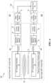
- FIG. 1illustrates a schematic timing diagram of a pulse sequence and a corresponding qualitative graph of an example method of plasma processing that includes source power pulses and bias power pulse in accordance with an embodiment of the invention
- FIG. 2illustrates a block diagram of an example plasma processing system including a source pulse modulation circuit and a pulse modulation timing circuit in accordance with an embodiment of the invention
- FIG. 3illustrates schematic timing diagrams of example methods of plasma processing including bias pulses with positive and negative leading offsets relative to source pulses in a accordance with embodiments of the invention
- FIG. 4illustrates schematic timing diagrams of example methods of plasma processing including bias pulses with negative and positive trailing offsets relative to source pulses in accordance with embodiments of the invention
- FIG. 5illustrates a schematic timing diagram of an example method of plasma processing including bias pulses with dynamic offsets relative to source pulses in accordance with an embodiment of the invention
- FIG. 6illustrates a schematic timing diagram of an example method of plasma processing include bias power pulse trains in accordance with an embodiment of the invention
- FIG. 7illustrates a schematic timing diagram of an example method of plasma processing including source pulse and bias pulse timing associated with particular gas flows in accordance with an embodiment of the invention
- FIG. 8illustrates a schematic diagram of an example capacitively coupled plasma processing system which may be used to perform methods of plasma processing in accordance with an embodiment of the invention
- FIG. 9illustrates a schematic diagram of an example inductively coupled plasma processing system which may be used to perform methods of plasma processing in accordance with an embodiment of the invention
- FIG. 10illustrates a schematic diagram of an example surface wave plasma processing system which may be used to perform methods of plasma processing in accordance with an embodiment of the invention
- FIG. 11illustrates a schematic diagram of an example remote plasma processing system which may be used to perform methods of plasma processing in accordance with an embodiment of the invention
- FIG. 12illustrates a block diagram of an example plasma processing system including a non-resonant source power coupling electrode in accordance with an embodiment of the invention
- FIG. 13illustrates a block diagram of an example plasma processing system including a resonant source power coupling electrode in accordance with an embodiment of the invention
- FIG. 14illustrates a schematic diagram of an example helical resonator plasma processing system in accordance with an embodiment of the invention
- FIG. 15illustrates an example method of plasma processing in accordance with an embodiment of the invention.
- FIG. 16illustrates several conventional timing diagrams including source power and bias power.
- Various techniquespertain to device fabrication using precision plasma processing techniques, including etch and deposition processes.
- FEOLfront end of line
- BEOLback end of line
- Conventional plasma processing apparatus and methodsmay be lacking in control of plasma properties, including control of radical populations and compositions, control of ion populations, and control of electron populations, as well as reaction by-products, and thus, have been deficient in meeting advanced scaling requirements.
- IEDFion energy distributions
- T iion temperature
- IADFion angular distributions
- EEDFelectron energy distributions
- T eelectron temperature
- Traditional plasma process parameterssuch as gas pressure, power, and more specifically, the manner in which electromagnetic fields are coupled to a gas environment in order to form plasma (e.g., capacitive coupling, inductive coupling, etc.) may impact these plasma properties.
- Various embodiments described hereinprovide systems and methods to control plasma properties for the delivery of ions for plasma processing such as in reactive ion etching or plasma deposition.
- the various embodimentsmay provide antiphased, antisynchronous, and/or out-of-phase source power and bias power pulsing for plasma processing.
- the pulsingmay be controlled using plasma processing parameters including pulse width, frequency, and amplitude for both source power and bias power as well as one or more offsets between pulses.
- bias power pulsesmay be pulsed in a delayed manner from the source plasma or at the same time as the source plasma.
- ion temperature T ielectron temperature T e
- electron density n eelectron density n e
- sheath voltage drop V sheathplasma bulk potential V P , and the like
- plasma propertiessuch as ion temperature T i , electron temperature T e , electron density n e , sheath voltage drop V sheath , plasma bulk potential V P , and the like may be modulated and controlled using the embodiment systems and methods as described herein.
- Embodiments provided belowdescribe various systems and methods of operating plasma processing systems, and in particular, methods of plasma processing that include source power pulses and bias power pulses.
- the following descriptiondescribes the embodiments.
- An example schematic timing diagram and a qualitative graph of an embodiment method of control for plasma processing that includes source power pulses and bias power pulsesare described using FIG. 1 .
- An embodiment plasma processing system including a source pulse modulation circuit and a pulse modulation timing circuitis described using FIG. 2 .
- Two embodiment methods of plasma processing including bias pulses with positive and negative leading offsets relative to source pulsesare described using FIG. 3 .
- Two embodiment methods of plasma processing including bias pulses with negative and positive trailing offsets relative to source pulsesare described using FIG. 4 .
- An embodiment method of plasma processing including bias pulses with dynamic offsetsis described using FIG.
- FIG. 5An embodiment method of plasma processing including bias power pulse trains is described using FIG. 6 .
- An embodiment method of plasma processing including source pulse and bias pulse timing associated with particular gas flowsis described using FIG. 7 .
- FIGS. 8 - 11Two embodiment plasma processing systems are described using FIGS. 8 - 11 .
- Two embodiment plasma processing systems including a source pulse modulation circuit and a pulse modulation timing circuitare described using FIGS. 12 and 13 .
- An embodiment helical resonator plasma processing systemis described using FIG. 14 .
- An embodiment method of plasma processingis described using FIG. 15 .
- FIG. 1illustrates a schematic timing diagram of a pulse sequence and a corresponding qualitative graph of an example method of control for plasma processing that includes source power pulses and bias power pulses in accordance with an embodiment of the invention.
- the source poweris coupled to a plasma processing chamber of a plasma processing system and is used to generate a plasma for processing of a microelectronic workpiece.
- the bias poweris also coupled to the plasma processing chamber and may be used to accelerate ions toward a surface of the microelectronic workpiece in addition to other functions.
- a timing diagram 100includes a source power 1 and a bias power 2 which are pulsed to generate and deliver ions to a microelectronic workpiece (e.g., a semiconductor wafer).
- timing diagram 100includes a pulse sequence with one or more source power (SP) pulses 11 and bias power (BP) pulses 12 which are at least partially non-overlapping in time.
- the source power 1may be alternating current (AC) power which is switched between an on state and an off state to generate the SP pulses 11 (the frequency of the AC power is higher than the frequency of the SP pulses 11 ).
- the bias power 2may also be AC power.
- one or both of the source power 1 and the bias power 2may be DC power.
- the pulse sequenceis periodic with a pulse modulation period 5 and includes multiple SP pulses 11 and BP pulses 12 .
- a pulse sequencemay refer to a single SP pulse and a single BP pulse.
- periodicitymay be beneficial, there is no strict requirement that the pulse sequence be periodic or that the SP pulses have the same period as the BP pulses.
- the temperature curve 31 and the density curve 32 of the generated plasmachange in accordance with the applied source power 1 of timing diagram 100 .
- SP pulses 11generate a plasma glow phase characterized by an increase in various plasma parameters such as the electron density n e , electron temperature T e , and the ion temperature T i .
- Initial application of a SP pulse 11may result in a spike 21 in plasma temperature (e.g., T e and T i ) which relaxes to a pseudo-equilibrium state 23 for the remainder of the SP pulse.
- the plasmaenters an afterglow phase during which the ions and electrons may cool down resulting in decreases in T e , T i .
- a BP pulseis applied to accelerate the generated ions towards a surface of a microelectronic workpiece.
- T e and T imay decrease more rapidly than n e in the afterglow phase. Since the electron density n e is correlated with available ions, applications of a BP pulse during the afterglow phase may be particularly effective in order to accelerate low-temperature ions to the surface of the microelectronic workpiece.
- the plasma currentmay also decrease. This current drop may allow for a large voltage difference V p across the plasma sheath and V DC (RF DC self-bias voltage) in the afterglow phase when bias power is applied (e.g., using a BP pulse).
- the increased voltage difference V p and the time-average drop dc voltage drop V DC along with the lower ion temperaturemay improve the directionality of the ion flux.
- the SP pulses and BP pulsesare at least partially non-overlapping in time.
- the SP pulses and BP pulsesare completely out-of-phase as illustrated in the timing diagram 100 .
- the SP pulses and BP pulsesmay partially overlap. Accordingly, embodiments of the method include both a nonzero interval of time during which the source power 1 is applied without the bias power 2 , as well as including a nonzero interval of time during which the bias power 2 is applied without the source power 1 .
- the pulse sequence of timing diagram 100may be generated using pulse modulation process parameters.
- the pulse modulation process parametersmay include SP pulse width 3 and SP pulse amplitude 4 corresponding to the source power 1 sequence as well as a leading edge bias offset 6 , BP pulse width 7 , BP pulse amplitude 8 , and a trailing edge bias offset 9 corresponding to the bias power 2 sequence.
- each SP pulse 11includes a SP pulse width 3 and an SP pulse amplitude 4 while each BP pulse 12 includes a BP pulse width 7 and a BP pulse amplitude 8 .
- amplitude as used hereinrefers to the average peak-to-peak amplitude of a given pulse.
- a specific pulse widthmay be implemented by choosing a duty cycle (%) for a given pulse modulation period 5 .
- a duty cycle (%)for a given pulse modulation period 5 .
- the pulse modulation periodis set to 150 ⁇ s
- a 56% source power duty cycle (%) and a 28% bias power duty cycle (%)would result in an 84 ⁇ s SP pulse width and a 42 ⁇ s BP pulse width.
- the source power 1 and the bias power 2have the same pulse modulation period.
- source power 1 and bias power 2may operate with separate pulse modulation period.
- the duty cycle (%) of either of the SP pulses 11 and BP pulses 12may range from about 3% to about 90%.
- the duty cycle (%) of the SP pulses 11is about 5%. In another embodiment, the duty cycle (%) of the SP pulses 11 is about 50%. In still another embodiment, the duty cycle (%) of both the SP pulses 11 and the BP pulses 12 is about 40%. Suitable duty cycles (%) for the SP pulses 11 and BP pulses 12 may be chosen according to specific properties of a given plasma process.
- the duration of any of the pulse widths described hereinmay have any suitable value as chosen based on specific parameters of a given plasma process.
- the SP pulse width 3may range between about 10 ⁇ s and about 100 ⁇ s.
- the SP pulse width 3may be larger or smaller.
- the SP pulse width 3may be on the order of milliseconds in some embodiments.
- the BP pulse width 7may range between 10 ⁇ s and about 100 ⁇ s, but can also be larger or smaller as with the SP pulse width 3 .
- the SP pulse width 3 and the BP pulse width 7may be independently chosen according to a given plasma process.
- a delay between SP pulses 11 and BP pulses 12may be referred to as a leading edge bias offset 6 .
- the leading edge bias offset 6may be implemented as a percentage of the pulse modulation period 5 .
- the leading edge bias offsetmay vary between ⁇ 10% to +10% of the pulse modulation period 5 .
- the leading edge bias offset 6may set as a specific time value. For example, continuing the above case where the source power 1 and the bias power 2 have the same pulse modulation period set to 150 ⁇ s, a leading edge bias offset of 10% would result in a 15 ⁇ s delay between the trailing edge of a SP pulse and a BP pulse.
- the leading edge bias offset 6is set to be positive. However, the leading edge bias offset 6 may also be zero or negative.
- a delay between BP pulses 12 and SP pulses 11may be referred to as a trailing edge bias offset 9 and may be implemented through a combination of the SP pulse width 3 , the leading edge bias offset 6 , and the BP pulse width 7 .
- a 56% source power duty cycle (%), a leading edge bias offset of 10%, and a 28% bias power duty cycle (%)accounts for 94% of a complete pulse modulation period. Therefore, in this specific example, there is a delay equal to 6% of the pulse modulation period between the trailing edge of a BP pulse and the leading edge of a SP pulse. Since the pulse modulation period is 150 ⁇ s, this delay which is the trailing edge bias offset 9 is equal to 9 ⁇ s. Similar to the leading edge bias offset 6 , the trailing edge bias offset 9 is not required to be positive, but may also be zero or negative.
- the duration of any of the offsets described hereinmay have any suitable value as chosen based on specific parameters of a given plasma process.
- the leading edge bias offset 6may range between about ⁇ 50 ⁇ s and about 50 ⁇ s. In various embodiments, the leading edge bias offset 6 may be between about ⁇ 15 ⁇ s and about 20 ⁇ s. In one embodiment, the leading edge bias offset 6 is about 20 ⁇ s. In another embodiment, the leading edge bias offset 6 is about to 10 ⁇ s. In still another embodiment, the leading edge bias offset 6 is about 1 ⁇ s.
- the pulse amplitudesmay have corresponding high and low amplitude states.
- the high and low amplitudesmay be voltage levels.
- each of the SP pulses 11may oscillate between a SP low amplitude state 13 and a SP high amplitude state 14 while each of the BP pulses 12 may oscillate between a BP low amplitude state 17 and a BP high amplitude state 18 .
- a positive or negative DC biasmay be applied to one or both the source power 1 or the bias power 2 so that the respective high and low amplitudes are brought to desirable levels.
- both the temperature curve 31 and density curve 32are qualitative in nature. Therefore, while both may be indicative of important phenomena associated with the effect of a pulse sequence on plasma parameters such as T e , T i , and n e , neither are intended to be drawn with a specific scale or be quantitatively accurate. Furthermore, simplifications may have been made for the sake of clarity.
- the electron temperature T e and the ion temperature T ihave been represented as a single curve in graph 102 because the shape of the curves is similar even though T e may be at least an order of magnitude greater than T i in a cold plasma.
- FIG. 2illustrates a block diagram of an example plasma processing system including a source pulse modulation circuit and a pulse modulation timing circuit in accordance with an embodiment of the invention.
- the plasma processing system of FIG. 2may be used to perform any of the embodiment methods as described herein, such as the method of FIG. 1 , for example.
- a plasma processing system 200includes a SP coupling electrode 15 coupled to a plasma processing chamber 210 .
- the plasma processing chamber 210may include a vacuum chamber.
- the SP coupling electrodemay allow application of source power to the plasma processing chamber 210 resulting in the generation of a plasma 60 .
- the SP coupling electrode 15is a conductive coil positioned around the plasma processing chamber 210 and is a quarter-wave helical resonator in one embodiment. In another embodiment, the SP coupling electrode 15 is a half-wave helical resonator.
- other SP coupling electrodesmay be employed, such as an antenna, plate electrode, or a waveguide, as examples.
- the plasma processing system 200further includes a BP coupling electrode 19 coupled to the plasma processing chamber 205 .
- the BP coupling electrode 19may enable application of bias power to a microelectronic workpiece being processed.
- the BP coupling electrode 19is a substrate holder and is an electrostatic chuck in one embodiment.
- the source powermay be coupled to the plasma processing chamber 210 using a SP control path 201 which includes a SP pulse modulation circuit 51 .
- the SP pulse modulation circuit 51may modulate a source signal between a SP high amplitude state 14 and a SP low amplitude state 13 .
- the modulated source signalmay correspond with the SP pulses 11 as described in reference to FIG. 1 .
- the modulated source signalmay be received by a SP function generator 20 which may superimpose a waveform onto the modulated source signal.
- a pulse modulation circuitsuch as the SP pulse modulation circuit 51
- a pulse modulation circuitcan be implemented, e.g., using a laser driver capable of generating high power pulses for laser diodes such as AVTECH AVOZ-D2-B pulse generator type circuits, for example.
- the SP function generator 20may also optionally include an amplification circuit such as an RF amplifier, configured to increase the amplitude of the modulated source signal.
- the SP function generator 20may be a signal generator, and may be a radio frequency (RF) signal generator in one embodiment.
- the SP function generator 20may be a microwave function generator.
- the SP function generator 20may be an arbitrary waveform generator (AWG).
- a function generator such as SP function generator 20may be a circuit that includes an electronic oscillator. More than one electronic oscillator may be included in a function generator. Waveforms may be generated by a function generator using digital signal processing. The digital output may then be converted with a digital-to-analog converter to produce an analog waveform.
- a function generatormay also include modulation functions such as amplitude modulation, frequency modulation, or phase modulation.
- the frequency of the superimposed waveformmay be higher than the pulse modulation frequency.
- the frequency of the superimposed waveformmay be an RF frequency and is about 13.56 MHz in one embodiment.
- each of the resulting SP pulsesmay include several cycles of the superimposed waveform.
- the waveform shapemay include a periodic waveform such as a sinusoidal wave, a square wave, a sawtooth wave, and the like.
- the waveform shapemay include an aperiodic wave such as a superposition of multiple sinusoidal waves of various frequencies to generate an arbitrary waveform shape.
- the SP control path 201may include an optional SP impedance matching network 25 .
- an impedance matching networksuch as the SP impedance matching network 25
- the matching circuitsmay be variations of L and T type networks.
- an impedance matching networkmay include a network of inductors, capacitors, and/or variable capacitors.
- Frequency tuningi.e., adjustment of the driving frequency to match the antenna-plasma resonance is another means of matching.
- Frequency tuning in pulsed modemay utilize feedback control to take advantage of power or voltage measurements that correlate with plasma impedance.
- the SP pulses generated by the SP function generator 20may pass through the optional SP impedance matching network 25 before being coupled to the plasma processing chamber 210 by the SP coupling electrode 15 .
- the optional SP impedance matching network 25may be omitted in certain plasma processing systems such as when the SP coupling electrode 15 is a resonant structure inductively coupled to the plasma 60 .
- the optional SP impedance matching network 25may be included when the SP coupling electrode 15 is non-resonant.
- the optional SP impedance matching network 25may be used to ensure that the source power is efficiently coupled to the plasma 60 by matching the impedance of the load to the impedance of the supply.
- the bias powermay be coupled to the plasma processing chamber 210 using a BP control path 202 .
- the BP control path 202may be coupled to the SP control path 201 through a pulse modulation timing circuit 52 .
- the pulse modulation timing circuit 52may determine the timing of BP pulses relative to the timing of SP pulses generated by the SP control path 201 .
- the pulse modulation timing circuit 52may receive a signal from the SP pulse modulation circuit 51 and introduce a delay triggered by either the leading edge or the trailing edge of a SP pulse.
- the signal from the SP pulse modulation circuit 51 to the pulse modulation timing circuit 52may be the SP pulse or a clock signal indicative of the SP pulse, as examples.
- the SP pulses and BP pulsesmay be offset from one another based on a timing schedule which may be implemented using clock signaling.
- the pulse modulation timing circuit 52may introduce a delay equal to 8% of the pulse modulation period after being triggered by the trailing edge of a SP pulse.
- the pulse modulation timing circuit 52is configured to be triggered by the leading edge of a SP pulse, a delay of 8% of the pulse modulation period plus the source power duty cycle (%) may be introduced by the pulse modulation timing circuit 52 .
- the pulse modulation timing circuit 52may determine the timing of SP pulses relative to the timing of BP pulses generated by the BP control path 202 .
- a timing circuitsuch as the pulse modulation timing circuit 52
- the pulse modulation timing circuit 52can be implemented using any timing circuit.
- a Highland Technology T560 4-channel compact digital delay and pulse generator circuitmay be used.
- the BP control path 202may include an optional BP pulse modulation circuit 53 triggered by the pulse modulation timing circuit 52 .
- the optional BP pulse modulation circuit 53may modulate a bias signal between a BP high amplitude state and a BP low amplitude state.
- the modulated bias signalmay correspond with the BP pulses 12 as described in reference to FIG. 1 .
- the optional BP pulse modulation circuit 53may be omitted and a delayed modulated source signal may correspond with the BP pulses.
- the modulated bias signalmay be received by an optional BP function generator 30 .
- the optional BP function generator 30may superimpose a waveform onto the modulated bias signal.
- the waveformmay be similar or different than the waveform superimposed on the modulated source signal and may have any desired waveform shape as previously described.
- the optional BP function generator 30may also optionally include an amplification circuit to increase the amplitude of the modulated bias signal.
- the bias power delivered to the plasma processing chamber 210is DC power.
- the optional BP function generator 30may be omitted.
- an amplification circuitmay be included instead of the optional BP function generator 30 .
- a BP impedance matching network 35is also included in the BP control path 202 between the optional BP function generator 30 and the BP coupling electrode 19 .
- the BP impedance matching networkmay be used to ensure that the bias power is efficiently coupled to the plasma processing chamber 210 by matching the impedance of the load to the impedance of the supply.
- the SP function generator 20 and the optional SP impedance matching network 25may be included in a SP generator circuit 240 which receives source power and provides SP pulses to the SP coupling electrode 15 .
- the optional BP function generator 30 and the BP impedance matching network 35may be included in a BP generator circuit 245 which receives bias power and provides BP pulses to the BP coupling electrode 19 .
- the SP pulse modulation circuit 51 , pulse modulation timing circuit 52 , and optional BP pulse modulation circuit 53may be included in a controller 250 .
- the controller 250may be locally located relative to the plasma processing chamber 210 .
- controller 250may be located remotely relative to the plasma processing chamber 210 .
- the controller 250may be capable of exchanging data with one or more of the elements included in the SP control path 201 and the BP control path 202 .
- Each of the impedance matching networksmay be controlled by controller 250 or may include a separate controller.
- the controller 250may be configured to set, monitor, and/or control various control parameters associated with generating a plasma and delivering ions to the surface of a microelectronic workpiece.
- Control parametersmay include, but are not limited to power level, frequency, and duty cycle (%) for both the source power and the bias power as well as bias offset percentage.
- Other control parameter setsmay also be used. For example, pulse width of the SP pulses and BP pulses and the bias offset may be entered directly rather than being represented as a duty cycle (%) of the pulse modulation period.
- FIG. 3illustrates schematic timing diagrams of example methods of plasma processing including bias pulses with positive and negative leading offsets relative to source pulses in accordance with embodiments of the invention.
- the timing diagrams of FIG. 3may be specific implementations of other embodiment timing diagrams, such as timing diagram 100 of FIG. 1 , for example.
- labeled elementsmay be as previously described.
- a timing diagram 300includes a positive leading edge (+LE) bias offset 306 between high amplitude states of SP pulses 11 and high amplitude states of non-overlapping BP pulses 312 which do not overlap in time with adjacent SP pulses 11 in the pulse sequence.
- the non-overlapping BP pulses 312also include a non-overlapping BP pulse width 307 and are separated from subsequent SP pulses 11 by a trailing edge bias offset 9 .
- timing diagram 320is similar to timing diagram 300 except that timing diagram 320 includes a negative leading edge ( ⁇ LE) bias offset 326 between high amplitude states of SP pulses 11 and high amplitude states of ⁇ LE BP pulses 322 which partially overlap in time with adjacent SP pulses 11 in the pulse sequence.
- ⁇ LE bias offset 326both the +LE bias offset 306 and the ⁇ LE bias offset 326 are measured relative to the trailing edge of a respective SP pulse 11 . Consequently, a negative offset such as ⁇ LE bias offset 326 results in ⁇ LE BP pulses 322 .
- the ⁇ LE BP pulses 322also include an overlapping BP pulse width 327 and are separated from subsequent SP pulses 11 by a trailing edge bias offset 9 .
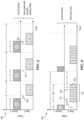
- FIG. 4illustrates schematic timing diagrams of example methods of plasma processing including bias pulses with negative and positive trailing offsets relative to source pulses in accordance with embodiments of the invention.
- the timing diagrams of FIG. 4may be specific implementations of other embodiment timing diagrams, such as timing diagram 100 of FIG. 1 , for example.
- labeled elementsmay be as previously described.
- a timing diagram 400includes a negative trailing edge ( ⁇ TE) bias offset 409 in addition to a +LE bias offset 306 .
- Each resulting ⁇ TE BP pulse 412 of the pulse sequencehas a ⁇ TE BP pulse width 407 and is non-overlapping in time with the previous SP pulse 11 , but partially overlapping in time with the subsequent SP pulse 11 .
- a negative offset valueindicates overlap with an adjacent pulse. Therefore, for trailing edge offsets of a given pulse, a negative offset results in overlap between the trailing edge of the pulse and the leading edge of the next pulse, as illustrated for ⁇ TE bias offset 409 in timing diagram 400 , for example.
- a timing diagram 420includes a negative ⁇ TE bias offset 409 in addition to a ⁇ LE bias offset 326 between high amplitude states of SP pulses 11 and high amplitude states of overlapping BP pulses 422 which partially overlap with both the previous and subsequent SP pulses 11 of the pulse sequence.
- the overlapping BP pulses 11include an overlapping BP pulse width 427 which is greater in duration than each SP pulse width 3 of the SP pulses 11 .
- FIG. 5illustrates a schematic timing diagram of an example method of plasma processing including bias pulses with dynamic offsets relative to source pulses in accordance with an embodiment of the invention.
- the timing diagram of FIG. 5may be a specific implementation of other embodiment timing diagrams, such as timing diagram 100 of FIG. 1 , for example.
- labeled elementsmay be as previously described.
- a timing diagram 500includes SP pulses 11 with pulse modulation period 5 and BP pulses 12 with variable leading offset bias offsets ( 509 , 519 , 529 ) that may be dynamically varied. Specifically, the leading edge bias offset of each of the BP pulses 12 may change for each SP pulse 11 of the pulse sequence. Any combination of positive, zero, and negative leading or trailing offsets are possible.
- the first BP pulse 12is illustrated with a positive variable offset 509
- the second and third BP pulses 12are illustrated with a zero value variable offset 519 and a negative variable offset 529 respectively.
- the offsetsmay change every pulse modulation period 5 , they may also stay the same for multiple pulse modulation periods at a time or change gradually. For example, a large positive offset may gradually be decreased in magnitude from period to period until it becomes zero and then negative.
- FIG. 6illustrates a schematic timing diagram of an example method of plasma processing include bias power pulse trains in accordance with an embodiment of the invention.
- the timing diagram of FIG. 6may be a specific implementation of other embodiment timing diagrams, such as timing diagram 100 of FIG. 1 , for example.
- labeled elementsmay be as previously described.
- a timing diagram 600includes SP pulses 11 and BP pulse trains 612 with BP pulse train width 607 .
- the BP pulse trains 612may be specific embodiments of BP pulses 12 as previously described.
- the BP pulse trains 612include BP subpulses 622 and corresponding BP subpulse width 617 and BP subpulse separation 619 .
- Each of the BP subpulses 622may be implemented similar to BP pulses 12 .
- the BP subpulses 622are AC pulses and are RF pulses in one embodiment. In another embodiment, the BP subpulses 622 are DC pulses.
- FIG. 7illustrates a schematic timing diagram of an example method of plasma processing including source pulse and bias pulse timing associated with particular gas flows in accordance with an embodiment of the invention.
- the timing diagram of FIG. 7may incorporate one or more specific implementations of other embodiment timing diagrams, such as timing diagram 100 of FIG. 1 .
- a given plasma processmay utilize multiple types of gas, each of which may have a specific implementation of an embodiment timing diagram associated with it.
- labeled elementsmay be as previously described.
- a timing diagram 700includes a gas source 701 in addition to a source power 1 and a bias power 2 .
- the gas source 701may include multiple gases and/or mixtures of gases.
- gas source 701includes a first gas (G1) flow 731 with a G1 gas flow duration 735 and a second gas (G2) flow 761 with a G2 gas flow duration 765 .
- the G1 gas flow 731 and the G2 gas flow 761are separated in time by a gas flow offset 740 .
- the second gasmay be introduced during the G1 gas flow 731 and the G2 gas flow 761 may partially overlap with the G2 gas flow 731 .
- Each of the gasesmay have a pulse sequence associated with the respective gas flow duration.
- a set of plasma processing parametersmay be chosen for each gas, for example, from prior embodiments such as in FIGS. 1 , and 3 - 6 , to generate a pulse sequence that is specifically tailored for a particular gas while it is being provided to the plasma processing chamber.
- the G1 pulse sequence 71 associated with the G1 gas flow 731includes G1 SP pulses 711 with G1 SP pulse width 703 and G1 BP pulses 712 with G1 BP pulse width 707 and G1 BP pulse amplitude 708 .
- the G1 BP pulses 712are temporally defined relative to the G1 SP pulses 711 by a G1 LE bias offset 706 and a G1 TE bias offset 709 .
- the G1 pulse sequence 71has a G1 pulse modulation period 705 and may be offset from the leading edge of the G1 gas flow 731 by a G1 LE source offset 736 .
- the G2 gas flow 761has an associated G2 pulse sequence 72 including G2 SP pulses 751 with G2 SP pulse width 743 and G2 BP pulses 752 with G2 BP pulse width 747 and G2 BP pulse amplitude 758 .
- the G2 BP pulses 752are temporally defined relative to the G2 SP pulses 751 by a G2 LE bias offset 746 and a G2 TE bias offset 749 .
- the G2 pulse sequence 72has a G2 pulse modulation period 745 and may be offset from the leading edge of the G2 gas flow 761 by a G2 LE source offset 766 .
- plasma processing parametersmay be different between gas flows. For example, pulse width, pulse amplitude, frequency, offset, and others for both source power and bias power may be varied along with the gas flow.
- FIG. 8illustrates a schematic diagram of an example capacitively coupled plasma processing system
- FIG. 9illustrates a schematic diagram of an example inductively coupled plasma processing system
- FIG. toillustrates a schematic diagram of an example surface wave plasma processing system
- FIG. 11illustrates a schematic diagram of an example remote plasma processing system which may be used to perform methods of plasma processing in accordance with embodiments of the invention.
- the plasma processing systems of FIGS. 8 - 11may each be a specific implementation of other embodiment plasma processing systems, such as the plasma processing system 200 of FIG. 2 , for example.
- labeled elementsmay be as previously described.
- a capacitively coupled plasma (CCP) processing system 800includes an AC source power supply 881 coupled to a SP generator circuit 240 that is coupled to an upper plate electrode (UEL) 815 and an AC bias power supply 882 coupled to a BP generator circuit 245 that is coupled to a lower plate electrode (LEL) 819 .
- the AC source power supply 881 and the AC bias power supply 882may respectively generate source power and bias power in accordance with the embodiments described previously such as in FIGS. 1 , 3 - 7 .
- a CCP 860is formed within a grounded plasma processing chamber 810 proximate a substrate 16 between the UEL 815 and the LEL 819 .
- the LEL 819may also serve as an electrostatic chuck (ESC) to support and retain the substrate 16 .
- plasmais formed by coupling RF power to at least one of the electrodes.
- the AC power coupled to the UEL 815may have a different RF frequency than the AC power coupled to LEL 819 .
- multiple RF power sourcesmay be coupled to the same electrode.
- direct current (DC) powermay be coupled to the upper electrode and/or the lower electrode.
- an inductively coupled plasma (ICP) processing system gooincludes AC source power supply 881 coupled to a SP generator circuit 240 that is coupled to an inductive electrode 915 and AC bias power supply 882 coupled to a BP generator circuit 245 that is coupled to an LEL 819 .
- the AC source power supply 881 and the AC bias power supply 882may respectively generate source power and bias power in accordance with the embodiments described previously such as in FIGS. 1 , 3 - 7 .
- An ICP 960is formed proximate a substrate 16 between the inductive electrode 915 (e.g., a planar, or solenoidal/helical coil or antenna) and the LEL 819 .
- a dielectric material 910separates the inductive electrode 915 from the ICP 960 . The dielectric material 910 may reduce and/or prevent capacitive coupling effects.
- a surface wave plasma (SWP) processing system 1000includes AC source power supply 881 coupled to a SP generator circuit 240 that is coupled to a microwave waveguide ( ⁇ -waveguide) 1014 and a slot antenna 1015 .
- the AC source power supply 881 and the AC bias power supply 882may respectively generate source power and bias power in accordance with the embodiments described previously such as in FIGS. 1 , and 3 - 7 .
- An SWP 1060is formed proximate a substrate 16 between the slot antenna 1015 and a LEL 819 .
- the SWP 1060is formed by coupling RF power at microwave frequencies through a coaxial line and the ⁇ -waveguide 1014 to the slot antenna 1015 .
- the slot antenna 1015may be implemented as a plate with holes or other structures.
- the slot antennamay be sandwiched between dielectric structures similar to dielectric material 910 of FIG. 9 so that microwaves may pass from the waveguide (center) radially outward from the center (e.g., through a ceramic structure with a dielectric constant such that the wavelength is reduced, through the antenna structures, and/or through another dielectric material).
- a remote plasma processing system 1100is similar to the ICP processing system 900 of FIG. 9 except that instead of a plasma being formed proximate a substrate, a remote plasma 1160 is formed in a region remote from a substrate 16 , for example, in a different plasma chamber or an isolated part of the plasma processing chamber 810 .
- the remote plasma 1160is separated or isolated from the substrate 16 by a particle isolation structure 1118 .
- the particle isolation structure 1118may be a filter, conduit, or orifice plate arranged to impede the transport of charged particles from the remote plasma source to the substrate 16 .
- the remote plasma 1160is an ICP.
- the remote plasma 1160may be a CCP, an SWP, etc.
- FIG. 12illustrates a block diagram of an example plasma processing system including a non-resonant source power coupling electrode in accordance with an embodiment of the invention.
- the plasma processing system of FIG. 12may be used to perform any of the embodiment methods as described herein, such as the method of FIG. 1 , for example.
- a non-resonant plasma processing system 1200includes a SP supply node 81 supplying source power 1 coupled to an non-resonant SP coupling electrode 1215 of a plasma processing chamber 1210 and a BP supply node 82 supplying bias power 2 coupled to a bias power coupling electrode 19 of the plasma processing chamber 1210 .
- the source power 1is coupled to the non-resonant SP coupling electrode 1215 through a SP control path 1201 which includes a SP controller 1226 configured to control source power settings.
- the SP controller 1226may adjust gain settings for a SP RF function generator and amplifier 1220 and impedance matching settings for a SP impedance matching network 1225 .
- bias power 2is coupled to BP coupling electrode 19 through a BP control path 1202 including a BP controller 1236 which controls bias settings of a BP RF function generator and amplifier 1230 and a BP impedance matching network 1235 .
- the SP impedance matching network 1225is included in order to efficiently provide source power to a plasma.
- the impedance of the load on the power supplyshould be the same as the impedance of the power supply itself.
- the impedance of the load on the power supplymay be influenced by the impedance of the plasma, which may depend on specific rapidly changing conditions such as chemistry, pressure, density, and others. Therefore, the SP impedance matching network 1225 may beneficially allow plasma conditions to vary while maintaining efficient power coupling of the source power 1 to the plasma 60 .
- a SP pulse signalis generated using a SP pulse modulation circuit 1251 which may receive one or more plasma processing parameters as inputs.
- the SP pulse modulation circuit 1251receives a SP pulse frequency f S and a SP pulse width t p,S .
- the SP pulse modulation circuit 1251then generates a SP pulse signal V(f S , t p,S ) using f S and t p,S .
- the SP pulse signal V(f S , t p,S )includes a high amplitude state of about 5 V and a low amplitude state of about 0 V.
- the SP pulse frequency f Scan range from about 0.1 Hz to about 10 kHz.
- the SP pulse frequency f Scan range from about 1 kHz to about 5 kHz.
- the SP RF function generator and amplifier 1220receives the source power 1 from the SP supply node 81 and the SP pulse signal V(f S , t p,S ) from the SP pulse modulation circuit 1251 and then generates SP pulses by amplifying and modulating the SP pulse signal V(f S , t p,S ) with a function.
- the power amplificationmay range from a few watts (e.g., 1-2 W) to greater than 1000 kW.
- the generated functionmay comprise an AC signal.
- the AC signalcan be generated at a source frequency, which can fall within the RF range, very-high frequency (VHF) range, or microwave (MW) range of the electromagnetic spectrum.
- the generated functionmay comprise a DC signal such as a pulsed DC signal.
- the SP pulsespass through the SP impedance matching network 1225 and to a SP directional coupler 1227 . Therefore, the SP directional coupler 1227 receives SP pulses with a time varying source voltage V S (t) and source current I S (t).
- the SP directional coupler 1227is configured to pass the SP pulses to the non-resonant SP coupling electrode 1215 .
- the SP directional coupler 1227is also coupled to the SP controller 1226 which may beneficially allow the SP controller 1226 to adjust source power settings based on a comparison of the forward source power P f,S and the reverse source power P r,S , as illustrated.
- the forward source power P f,Smay be an indication of the magnitude of the power being transmitted in a forward direction (i.e., toward the SP coupling electrode) while the reverse source power P r,S may be an indication of the magnitude of the power being reflected in a reverse direction (i.e., away from the SP coupling electrode).
- P f,S and P r,Smay be measured by the SP controller 1226 .
- a similar feedback mechanismmay be implemented between the BP controller 1236 and a BP directional coupler 1237 that receives time varying bias voltage V B (t) and bias current I B (t) so that bias power settings may be adjusted based on a comparison of the forward bias power P f,B and the reverse bias power P r,B .
- P f,B and P r,Bmay be measured by the BP controller 1236 .
- the SP RF function generator and amplifier 1220 , the SP impedance matching network 1225 , the SP controller 1226 , and the SP directional coupler 1227are included in a non-resonant SP generator circuit 1240 which receives the source power 1 from the SP supply node 81 and provides SP pulses to the non-resonant SP coupling electrode 1215 .
- the non-resonant SP generator circuit 1240may be a specific implementation of the SP generator circuit 240 of FIG. 2 , for example.
- BP RF function generator and amplifier 1230the BP impedance matching network 1235 , the BP controller 1236 , and the BP directional coupler 1237 are included in a BP generator circuit 1245 which receives the bias power 2 from the BP supply node 82 and provides BP pulses to the BP coupling electrode 19 .
- the BP generator circuit 1245may be a specific implementation of the BP generator circuit 245 of FIG. 2 , for example.
- a time delay t delayis introduced between the SP pulses and BP pulses using a BP t delay timing circuit 1252 coupled to an output of the SP pulse modulation circuit 1251 .
- the SP pulse modulation circuit 1251may transmit a signal to the BP t delay timing circuit 1252 , where the signal may be the SP pulse or a clock signal indicative of the SP pulse.
- the BP t delay timing circuit 1252receives the time delay t delay at an input and then sends a signal to the BP pulse modulation circuit 1253 .
- the BP t delay timing circuit 1252is triggered by the trailing edge of the SP pulse signal.
- the BP t delay timing circuit 1252may be triggered by the leading edge of the SP pulse signal.
- the BP pulse modulation circuit 1253generates a BP pulse signal using inputs (e.g., BP pulse frequency f B and BP pulse width t p,B ) which is then sent to the BP RF function generator and amplifier 1230 .
- inputse.g., BP pulse frequency f B and BP pulse width t p,B
- an alternating time delaymay be used.
- a specific time delaymay correspond to each gas or combination of gases during a given plasma process.
- other plasma processing parametersmay change for a particular gas or combination of gases such as the SP pulse frequency f S s, the SP pulse width t p,S , the BP pulse frequency f B , the BP pulse width t p,B , and others.
- the function generated by the BP RF function generator and amplifier 1230may comprise an AC signal.
- the AC signalcan be generated at a bias frequency, which can also fall within the RF range, VHF range, or MW range.
- the source frequencycan exceed about 10 MHz, and the bias frequency can be less than about 15 MHz.
- the source frequencycan exceed about 50 MHz, and the bias frequency can be less than about 5 MHz.
- the source frequencycan range from about 50 MHz to about 150 MHz, and the bias frequency can range from about 1 MHz to about 5 MHz.
- FIG. 13illustrates a block diagram of an example plasma processing system including a resonant source power coupling electrode in accordance with an embodiment of the invention.
- the plasma processing system of FIG. 13may be used to perform any of the embodiment methods as described herein, such as the method of FIG. 1 , for example.
- a resonant plasma processing system 1300includes a SP control path 1301 which includes a resonant SP coupling electrode 1315 .
- the resonant plasma processing system 1300is similar the non-resonant plasma processing system 1200 except that the SP impedance matching network 1225 is omitted in the SP control path 1301 because the resonant SP coupling electrode 1315 may provide the advantage of efficient source power coupling to a plasma 60 without impedance matching.
- a SP RF function generator and amplifier 1220provides SP pulses directly to a SP directional coupler 1227 which may provide feedback to a SP controller 1327 .
- the SP RF function generator and amplifier 1220 , the SP controller 1226 , and the SP directional coupler 1227are included in a resonant SP generator circuit 1340 which receives the source power 1 from the SP supply node 81 and provides SP pulses to the resonant SP coupling electrode 1315 .
- the resonant SP generator circuit 1340may be a specific implementation of the SP generator circuit 240 of FIG. 2 , for example.
- the resonant plasma processing system 1300may also advantageously enable agile pulsing of the source power.
- impedance matching networksmay be unable to respond as quickly as a matchless resonant structure such as the resonant SP coupling electrode 1315 . Therefore, at higher SP pulse frequencies, impedance matching networks may be limited to lower frequencies in order to provide efficient source power to the plasma.
- the resonant SP coupling electrode 1315comprises a helical resonator antenna 1329 .
- FIG. 14illustrates a schematic diagram of an example helical resonator plasma processing system in accordance with an embodiment of the invention.
- the helical resonator plasma processing systemmay be a specific implementation of other plasma processing systems such as the plasma processing system 200 of FIG. 2 , the ICP processing system 900 of FIG. 9 and/or the resonant plasma processing system 1300 of FIG. 13 , as examples.
- the source power coupling electrodeis formed as a helical resonator antenna.
- labeled elementsmay be as previously described.
- a helical resonator plasma processing system 1400includes a grounded outer structure 1410 surrounding a resonant SP coupling electrode 1315 implemented as a helical resonator antenna 1329 which in turn surrounds a dielectric inner surface 1411 .
- the helical resonator antenna 1329is grounded at one end and left free at the other.
- An AC source power supply 881is coupled to a SP generator circuit 240 which is coupled to the helical resonator antenna 1329 at an appropriate distance from the grounded connection.
- the source power coupling location(also referred to as a tap position) may depend on operating frequency as well as other considerations.
- a helical resonator plasma 1460is generated which is inductively coupled to the resonant SP coupling electrode 1315 .
- the dielectric inner surface 1411may be provided between the helical resonator plasma 1460 and the helical resonator antenna 1329 to facilitate inductive coupling.
- An AC bias power supply 882may be coupled to a BP generator circuit 245 which is coupled to a lower plate electrode (LEL) 819 .
- the lower plate electrode (LEL) 819serves as an electrostatic chuck (ESC) to support and retain a substrate 16 .
- the helical resonator antenna 1329may be a full-wave, half-wave, or quarter-wave antenna. For example, if the helical resonator antenna 1329 is driven at using RF power with a frequency of 13.56 MHz, a quarter-wave helical resonator antenna may be about 5.5 m in length. As the RF frequency increases, the length of the helical resonator antenna 1329 may decrease. For example, a quarter-wave helical resonator antenna driven at about 50 MHz may be about 1.5 m in length.
- FIG. 15illustrates an example method of plasma processing in accordance with an embodiment of the invention.
- the method of FIG. 15may be performed by any of the embodiment plasma processing systems as described herein, such as plasma processing system 200 of FIG. 2 , for example. It is noted that FIG. 15 is not intended to limit method steps to a particular order. Additionally, any of the steps as described in FIG. 15 may be performed concurrently in any combination as well as separately. Accordingly, variation of the ordering and/or timing of the below method steps is within the scope of the method as described as may be apparent to a person of skill in the art.
- Step 1501 of a method 1500 of plasma processingincludes outputting a signal to a function generator using a pulse modulation circuit.
- Step 1502includes generating a SP pulse using the function generator in response to outputting the signal.
- Step 1503includes providing the SP pulse at a SP coupling electrode of a plasma processing chamber to generate a plasma.
- Step 1504includes generating a BP pulse by triggering a delay relative to the SP pulse.
- Step 1505includes providing the BP pulse at a BP coupling electrode of the plasma processing chamber.
- Step 1506includes performing a plasma deposition or etch process on a substrate disposed in the plasma processing chamber where providing the BP pulse accelerates ions from the plasma towards the substrate.
- a plasma processing systemincluding a vacuum chamber; a first coupling electrode configured to provide power for generation of a plasma in the vacuum chamber, the first coupling electrode being further configured to couple SP pulses to the plasma; a substrate holder disposed in the vacuum chamber, the substrate holder being configured to support a substrate; a second coupling electrode configured to couple BP pulses to the substrate; and a controller configured to control a first offset duration between the SP pulses the BP pulses.
- the plasma processing system of example 3further including a second pulse modulation circuit coupled to the timing circuit; and a second function generator coupled to the second pulse modulation circuit and configured to generate the BP pulses.
- timing circuitis further configured to control a second offset duration between the BP pulses and the SP pulses.
- the first pulse modulation circuitincludes a first input configured to receive a first pulse frequency, and a second input configured to receive a first pulse width, and wherein the first pulse modulation circuit is further configured to generate a SP pulse signal at an output based on the first pulse frequency and the first pulse width.
- timing circuitincludes a timing circuit input configured to receive a time delay, and wherein the timing circuit is further configured to set the first offset duration based on the time delay.
- ACalternating current
- the plasma processing system of example 8further including a second pulse modulation circuit coupled to the timing circuit and configured to generate a BP pulse signal; and a second function generator coupled to the second pulse modulation circuit and configured to generate the BP pulses by modulating the BP pulse signal with an AC signal generated at a second frequency, wherein the second frequency is less than about 15 MHz, and wherein the first frequency is greater than about 10 MHz.
- An apparatusincluding a vacuum chamber; a coupling electrode coupled to a source power (SP) supply node and configured to generate a plasma within the vacuum chamber using a first sequence of SP pulses; and a substrate holder coupled to a bias power (BP) supply node and disposed within the vacuum chamber, the substrate holder being configured to support a substrate to be processed by the plasma, wherein a second sequence of BP pulses is configured to accelerate ions of the plasma towards the substrate.
- SPsource power
- BPbias power
- the apparatus of example 12further including a function generator; and a directional coupler including an output directly coupled to the resonant coupling electrode and an input directly coupled to the function generator.
- the apparatus of example tofurther including a function generator; an impedance matching network coupled to the function generator; and a directional coupler including an input coupled to the impedance matching network, wherein the coupling electrode is a non-resonant coupling electrode, and wherein the directional coupler further includes an output coupled to the non-resonant coupling electrode.
- a method of plasma processingincluding using a first pulse modulation circuit, outputting a first signal to a first function generator; generating a first source power (SP) pulse using the first function generator in response to the outputting the first signal; providing the first SP pulse at a first coupling electrode of a vacuum chamber to generate a plasma; generating a bias power (BP) pulse by triggering a delay relative to the first SP pulse; providing the BP pulse at a second coupling electrode of the vacuum chamber; and performing a plasma deposition or etch process on a substrate disposed in the vacuum chamber, wherein providing the BP pulse accelerates ions from the plasma towards the substrate.
- SPsource power
- BPbias power
- the delayincludes an offset duration between about ⁇ 15 ⁇ s and about 20 ⁇ s; and a leading edge of the BP pulse is separated from a trailing edge of the first SP pulse by the offset duration.
- the power control techniques as described hereinmay be controlled by a controller.
- the controllermay be implemented using one or more programmable integrated circuits that are programmed to provide the functionality described herein.
- processorse.g., microprocessor, microcontroller, central processing unit, etc.
- programmable logic devicese.g., CPLD (complex programmable logic device), FPGA (field programmable gate array), etc.
- CPLDcomplex programmable logic device
- FPGAfield programmable gate array
- other programmable integrated circuitsmay be programmed with software or other programming instructions to implement any of the functionality described herein.
- the software or other programming instructionsmay be stored in one or more non-transitory computer-readable mediums (e.g., memory storage devices, FLASH memory, DRAM memory, reprogrammable storage devices, hard drives, floppy disks, DVDs, CD-ROMs, etc.), and the software or other programming instructions, when executed by the programmable integrated circuits, cause the programmable integrated circuits to perform the processes, functions, and/or capabilities described herein. Other variations of the above could also be implemented.
- non-transitory computer-readable mediumse.g., memory storage devices, FLASH memory, DRAM memory, reprogrammable storage devices, hard drives, floppy disks, DVDs, CD-ROMs, etc.
- One or more deposition processesmay be used to form material layers using the plasma process described herein.
- a precursor gas mixturemay be used including but not limited to hydrocarbons, fluorocarbons, or nitrogen containing hydrocarbons in combination with one or more dilution gases (e.g., argon, nitrogen, etc.) at a variety of pressure, power, flow and temperature conditions.
- one or more etch processesmay be used to etch material layers using the plasma process described herein.
- plasma etch processesmay be implemented using plasma containing fluorocarbons, oxygen, nitrogen, hydrogen, argon, and/or other gases.
- operating variables for process stepsfor example, the chamber temperature, chamber pressure, flowrates of gases, frequency and/or power applied to electrode assembly in the generation of plasma, and/or other operating variables for the processing steps may be controlled. Variations of the above may also be implemented while still taking advantage of the techniques described herein.
Landscapes
- Engineering & Computer Science (AREA)
- Chemical & Material Sciences (AREA)
- Physics & Mathematics (AREA)
- Plasma & Fusion (AREA)
- Analytical Chemistry (AREA)
- Microelectronics & Electronic Packaging (AREA)
- Condensed Matter Physics & Semiconductors (AREA)
- Power Engineering (AREA)
- Computer Hardware Design (AREA)
- Manufacturing & Machinery (AREA)
- General Physics & Mathematics (AREA)
- Organic Chemistry (AREA)
- Chemical Kinetics & Catalysis (AREA)
- Materials Engineering (AREA)
- Metallurgy (AREA)
- General Chemical & Material Sciences (AREA)
- Mechanical Engineering (AREA)
- Electromagnetism (AREA)
- Plasma Technology (AREA)
- Drying Of Semiconductors (AREA)
- Chemical Vapour Deposition (AREA)
Abstract
Description
Claims (18)
Priority Applications (7)
| Application Number | Priority Date | Filing Date | Title |
|---|---|---|---|
| US16/219,535US12230475B2 (en) | 2018-08-14 | 2018-12-13 | Systems and methods of control for plasma processing |
| PCT/US2019/045756WO2020036806A1 (en) | 2018-08-14 | 2019-08-08 | Systems and methods of control for plasma processing |
| JP2021507606AJP7397247B2 (en) | 2018-08-14 | 2019-08-08 | Control system and method for plasma processing |
| CN201980045152.4ACN112424904B (en) | 2018-08-14 | 2019-08-08 | System and method for controlling plasma processing |
| KR1020217003893AKR20210032420A (en) | 2018-08-14 | 2019-08-08 | Control system and method for plasma process |
| TW108128854ATWI856020B (en) | 2018-08-14 | 2019-08-14 | Systems and methods of control for plasma processing |
| US19/019,200US20250149295A1 (en) | 2018-08-14 | 2025-01-13 | Systems and methods of control for plasma processing |
Applications Claiming Priority (3)
| Application Number | Priority Date | Filing Date | Title |
|---|---|---|---|
| US201862718454P | 2018-08-14 | 2018-08-14 | |
| US201862724879P | 2018-08-30 | 2018-08-30 | |
| US16/219,535US12230475B2 (en) | 2018-08-14 | 2018-12-13 | Systems and methods of control for plasma processing |
Related Child Applications (1)
| Application Number | Title | Priority Date | Filing Date |
|---|---|---|---|
| US19/019,200ContinuationUS20250149295A1 (en) | 2018-08-14 | 2025-01-13 | Systems and methods of control for plasma processing |
Publications (2)
| Publication Number | Publication Date |
|---|---|
| US20200058469A1 US20200058469A1 (en) | 2020-02-20 |
| US12230475B2true US12230475B2 (en) | 2025-02-18 |
Family
ID=69523348
Family Applications (3)
| Application Number | Title | Priority Date | Filing Date |
|---|---|---|---|
| US16/219,535Active2040-08-19US12230475B2 (en) | 2018-08-14 | 2018-12-13 | Systems and methods of control for plasma processing |
| US16/221,971ActiveUS10998169B2 (en) | 2018-08-14 | 2018-12-17 | Systems and methods of control for plasma processing |
| US19/019,200PendingUS20250149295A1 (en) | 2018-08-14 | 2025-01-13 | Systems and methods of control for plasma processing |
Family Applications After (2)
| Application Number | Title | Priority Date | Filing Date |
|---|---|---|---|
| US16/221,971ActiveUS10998169B2 (en) | 2018-08-14 | 2018-12-17 | Systems and methods of control for plasma processing |
| US19/019,200PendingUS20250149295A1 (en) | 2018-08-14 | 2025-01-13 | Systems and methods of control for plasma processing |
Country Status (6)
| Country | Link |
|---|---|
| US (3) | US12230475B2 (en) |
| JP (1) | JP7397247B2 (en) |
| KR (2) | KR20210032420A (en) |
| CN (1) | CN112424904B (en) |
| TW (1) | TWI856020B (en) |
| WO (2) | WO2020036806A1 (en) |
Families Citing this family (306)
| Publication number | Priority date | Publication date | Assignee | Title |
|---|---|---|---|---|
| US20130023129A1 (en) | 2011-07-20 | 2013-01-24 | Asm America, Inc. | Pressure transmitter for a semiconductor processing environment |
| US20160376700A1 (en) | 2013-02-01 | 2016-12-29 | Asm Ip Holding B.V. | System for treatment of deposition reactor |
| US10941490B2 (en) | 2014-10-07 | 2021-03-09 | Asm Ip Holding B.V. | Multiple temperature range susceptor, assembly, reactor and system including the susceptor, and methods of using the same |
| US10276355B2 (en) | 2015-03-12 | 2019-04-30 | Asm Ip Holding B.V. | Multi-zone reactor, system including the reactor, and method of using the same |
| US9828672B2 (en) | 2015-03-26 | 2017-11-28 | Lam Research Corporation | Minimizing radical recombination using ALD silicon oxide surface coating with intermittent restoration plasma |
| US11139308B2 (en) | 2015-12-29 | 2021-10-05 | Asm Ip Holding B.V. | Atomic layer deposition of III-V compounds to form V-NAND devices |
| US10529554B2 (en) | 2016-02-19 | 2020-01-07 | Asm Ip Holding B.V. | Method for forming silicon nitride film selectively on sidewalls or flat surfaces of trenches |
| US10343920B2 (en) | 2016-03-18 | 2019-07-09 | Asm Ip Holding B.V. | Aligned carbon nanotubes |
| US11453943B2 (en) | 2016-05-25 | 2022-09-27 | Asm Ip Holding B.V. | Method for forming carbon-containing silicon/metal oxide or nitride film by ALD using silicon precursor and hydrocarbon precursor |
| US10612137B2 (en) | 2016-07-08 | 2020-04-07 | Asm Ip Holdings B.V. | Organic reactants for atomic layer deposition |
| US9859151B1 (en) | 2016-07-08 | 2018-01-02 | Asm Ip Holding B.V. | Selective film deposition method to form air gaps |
| US9887082B1 (en) | 2016-07-28 | 2018-02-06 | Asm Ip Holding B.V. | Method and apparatus for filling a gap |
| US9812320B1 (en) | 2016-07-28 | 2017-11-07 | Asm Ip Holding B.V. | Method and apparatus for filling a gap |
| US11532757B2 (en) | 2016-10-27 | 2022-12-20 | Asm Ip Holding B.V. | Deposition of charge trapping layers |
| US10714350B2 (en) | 2016-11-01 | 2020-07-14 | ASM IP Holdings, B.V. | Methods for forming a transition metal niobium nitride film on a substrate by atomic layer deposition and related semiconductor device structures |
| KR102546317B1 (en) | 2016-11-15 | 2023-06-21 | 에이에스엠 아이피 홀딩 비.브이. | Gas supply unit and substrate processing apparatus including the same |
| US11447861B2 (en) | 2016-12-15 | 2022-09-20 | Asm Ip Holding B.V. | Sequential infiltration synthesis apparatus and a method of forming a patterned structure |
| US11581186B2 (en) | 2016-12-15 | 2023-02-14 | Asm Ip Holding B.V. | Sequential infiltration synthesis apparatus |
| US11390950B2 (en) | 2017-01-10 | 2022-07-19 | Asm Ip Holding B.V. | Reactor system and method to reduce residue buildup during a film deposition process |
| US10468261B2 (en) | 2017-02-15 | 2019-11-05 | Asm Ip Holding B.V. | Methods for forming a metallic film on a substrate by cyclical deposition and related semiconductor device structures |
| US10770286B2 (en) | 2017-05-08 | 2020-09-08 | Asm Ip Holdings B.V. | Methods for selectively forming a silicon nitride film on a substrate and related semiconductor device structures |
| US12040200B2 (en) | 2017-06-20 | 2024-07-16 | Asm Ip Holding B.V. | Semiconductor processing apparatus and methods for calibrating a semiconductor processing apparatus |
| US11306395B2 (en) | 2017-06-28 | 2022-04-19 | Asm Ip Holding B.V. | Methods for depositing a transition metal nitride film on a substrate by atomic layer deposition and related deposition apparatus |
| KR20190009245A (en) | 2017-07-18 | 2019-01-28 | 에이에스엠 아이피 홀딩 비.브이. | Methods for forming a semiconductor device structure and related semiconductor device structures |
| US11374112B2 (en) | 2017-07-19 | 2022-06-28 | Asm Ip Holding B.V. | Method for depositing a group IV semiconductor and related semiconductor device structures |
| US10590535B2 (en) | 2017-07-26 | 2020-03-17 | Asm Ip Holdings B.V. | Chemical treatment, deposition and/or infiltration apparatus and method for using the same |
| TWI815813B (en) | 2017-08-04 | 2023-09-21 | 荷蘭商Asm智慧財產控股公司 | Showerhead assembly for distributing a gas within a reaction chamber |
| US10692741B2 (en) | 2017-08-08 | 2020-06-23 | Asm Ip Holdings B.V. | Radiation shield |
| US10770336B2 (en) | 2017-08-08 | 2020-09-08 | Asm Ip Holding B.V. | Substrate lift mechanism and reactor including same |
| US11769682B2 (en) | 2017-08-09 | 2023-09-26 | Asm Ip Holding B.V. | Storage apparatus for storing cassettes for substrates and processing apparatus equipped therewith |
| US11830730B2 (en) | 2017-08-29 | 2023-11-28 | Asm Ip Holding B.V. | Layer forming method and apparatus |
| US11295980B2 (en) | 2017-08-30 | 2022-04-05 | Asm Ip Holding B.V. | Methods for depositing a molybdenum metal film over a dielectric surface of a substrate by a cyclical deposition process and related semiconductor device structures |
| US10510575B2 (en) | 2017-09-20 | 2019-12-17 | Applied Materials, Inc. | Substrate support with multiple embedded electrodes |
| US10658205B2 (en) | 2017-09-28 | 2020-05-19 | Asm Ip Holdings B.V. | Chemical dispensing apparatus and methods for dispensing a chemical to a reaction chamber |
| US10403504B2 (en) | 2017-10-05 | 2019-09-03 | Asm Ip Holding B.V. | Method for selectively depositing a metallic film on a substrate |
| US10923344B2 (en) | 2017-10-30 | 2021-02-16 | Asm Ip Holding B.V. | Methods for forming a semiconductor structure and related semiconductor structures |
| CN111344522B (en) | 2017-11-27 | 2022-04-12 | 阿斯莫Ip控股公司 | Including clean mini-environment device |
| WO2019103613A1 (en) | 2017-11-27 | 2019-05-31 | Asm Ip Holding B.V. | A storage device for storing wafer cassettes for use with a batch furnace |
| US10760158B2 (en) | 2017-12-15 | 2020-09-01 | Lam Research Corporation | Ex situ coating of chamber components for semiconductor processing |
| US10872771B2 (en) | 2018-01-16 | 2020-12-22 | Asm Ip Holding B. V. | Method for depositing a material film on a substrate within a reaction chamber by a cyclical deposition process and related device structures |
| KR102695659B1 (en) | 2018-01-19 | 2024-08-14 | 에이에스엠 아이피 홀딩 비.브이. | Method for depositing a gap filling layer by plasma assisted deposition |
| TWI799494B (en) | 2018-01-19 | 2023-04-21 | 荷蘭商Asm 智慧財產控股公司 | Deposition method |
| US11081345B2 (en) | 2018-02-06 | 2021-08-03 | Asm Ip Holding B.V. | Method of post-deposition treatment for silicon oxide film |
| US10896820B2 (en) | 2018-02-14 | 2021-01-19 | Asm Ip Holding B.V. | Method for depositing a ruthenium-containing film on a substrate by a cyclical deposition process |
| WO2019158960A1 (en) | 2018-02-14 | 2019-08-22 | Asm Ip Holding B.V. | A method for depositing a ruthenium-containing film on a substrate by a cyclical deposition process |
| US10731249B2 (en) | 2018-02-15 | 2020-08-04 | Asm Ip Holding B.V. | Method of forming a transition metal containing film on a substrate by a cyclical deposition process, a method for supplying a transition metal halide compound to a reaction chamber, and related vapor deposition apparatus |
| KR102636427B1 (en) | 2018-02-20 | 2024-02-13 | 에이에스엠 아이피 홀딩 비.브이. | Substrate processing method and apparatus |
| US10975470B2 (en) | 2018-02-23 | 2021-04-13 | Asm Ip Holding B.V. | Apparatus for detecting or monitoring for a chemical precursor in a high temperature environment |
| US11473195B2 (en) | 2018-03-01 | 2022-10-18 | Asm Ip Holding B.V. | Semiconductor processing apparatus and a method for processing a substrate |
| KR102646467B1 (en) | 2018-03-27 | 2024-03-11 | 에이에스엠 아이피 홀딩 비.브이. | Method of forming an electrode on a substrate and a semiconductor device structure including an electrode |
| KR102600229B1 (en) | 2018-04-09 | 2023-11-10 | 에이에스엠 아이피 홀딩 비.브이. | Substrate supporting device, substrate processing apparatus including the same and substrate processing method |
| US12025484B2 (en) | 2018-05-08 | 2024-07-02 | Asm Ip Holding B.V. | Thin film forming method |
| US12272527B2 (en) | 2018-05-09 | 2025-04-08 | Asm Ip Holding B.V. | Apparatus for use with hydrogen radicals and method of using same |
| US10555412B2 (en) | 2018-05-10 | 2020-02-04 | Applied Materials, Inc. | Method of controlling ion energy distribution using a pulse generator with a current-return output stage |
| KR102596988B1 (en) | 2018-05-28 | 2023-10-31 | 에이에스엠 아이피 홀딩 비.브이. | Method of processing a substrate and a device manufactured by the same |
| US11718913B2 (en) | 2018-06-04 | 2023-08-08 | Asm Ip Holding B.V. | Gas distribution system and reactor system including same |
| US10797133B2 (en) | 2018-06-21 | 2020-10-06 | Asm Ip Holding B.V. | Method for depositing a phosphorus doped silicon arsenide film and related semiconductor device structures |
| KR102568797B1 (en) | 2018-06-21 | 2023-08-21 | 에이에스엠 아이피 홀딩 비.브이. | Substrate processing system |
| TWI873894B (en) | 2018-06-27 | 2025-02-21 | 荷蘭商Asm Ip私人控股有限公司 | Cyclic deposition methods for forming metal-containing material and films and structures including the metal-containing material |
| KR102854019B1 (en) | 2018-06-27 | 2025-09-02 | 에이에스엠 아이피 홀딩 비.브이. | Periodic deposition method for forming a metal-containing material and films and structures comprising the metal-containing material |
| US10755922B2 (en) | 2018-07-03 | 2020-08-25 | Asm Ip Holding B.V. | Method for depositing silicon-free carbon-containing film as gap-fill layer by pulse plasma-assisted deposition |
| US10388513B1 (en) | 2018-07-03 | 2019-08-20 | Asm Ip Holding B.V. | Method for depositing silicon-free carbon-containing film as gap-fill layer by pulse plasma-assisted deposition |
| US11430674B2 (en) | 2018-08-22 | 2022-08-30 | Asm Ip Holding B.V. | Sensor array, apparatus for dispensing a vapor phase reactant to a reaction chamber and related methods |
| KR102707956B1 (en) | 2018-09-11 | 2024-09-19 | 에이에스엠 아이피 홀딩 비.브이. | Method for deposition of a thin film |
| US11024523B2 (en) | 2018-09-11 | 2021-06-01 | Asm Ip Holding B.V. | Substrate processing apparatus and method |
| CN110970344B (en) | 2018-10-01 | 2024-10-25 | Asmip控股有限公司 | Substrate holding apparatus, system comprising the same and method of using the same |
| KR102592699B1 (en) | 2018-10-08 | 2023-10-23 | 에이에스엠 아이피 홀딩 비.브이. | Substrate support unit and apparatuses for depositing thin film and processing the substrate including the same |
| KR102546322B1 (en) | 2018-10-19 | 2023-06-21 | 에이에스엠 아이피 홀딩 비.브이. | Substrate processing apparatus and substrate processing method |
| KR20250110938A (en)* | 2018-10-19 | 2025-07-21 | 램 리써치 코포레이션 | In situ protective coating of chamber components for semiconductor processing |
| US12378665B2 (en) | 2018-10-26 | 2025-08-05 | Asm Ip Holding B.V. | High temperature coatings for a preclean and etch apparatus and related methods |
| US11087997B2 (en) | 2018-10-31 | 2021-08-10 | Asm Ip Holding B.V. | Substrate processing apparatus for processing substrates |
| KR102748291B1 (en) | 2018-11-02 | 2024-12-31 | 에이에스엠 아이피 홀딩 비.브이. | Substrate support unit and substrate processing apparatus including the same |
| US11572620B2 (en) | 2018-11-06 | 2023-02-07 | Asm Ip Holding B.V. | Methods for selectively depositing an amorphous silicon film on a substrate |
| US10818758B2 (en) | 2018-11-16 | 2020-10-27 | Asm Ip Holding B.V. | Methods for forming a metal silicate film on a substrate in a reaction chamber and related semiconductor device structures |
| US11476145B2 (en) | 2018-11-20 | 2022-10-18 | Applied Materials, Inc. | Automatic ESC bias compensation when using pulsed DC bias |
| US12040199B2 (en) | 2018-11-28 | 2024-07-16 | Asm Ip Holding B.V. | Substrate processing apparatus for processing substrates |
| KR102636428B1 (en) | 2018-12-04 | 2024-02-13 | 에이에스엠 아이피 홀딩 비.브이. | A method for cleaning a substrate processing apparatus |
| US11158513B2 (en) | 2018-12-13 | 2021-10-26 | Asm Ip Holding B.V. | Methods for forming a rhenium-containing film on a substrate by a cyclical deposition process and related semiconductor device structures |
| TWI874340B (en) | 2018-12-14 | 2025-03-01 | 荷蘭商Asm Ip私人控股有限公司 | Method of forming device structure, structure formed by the method and system for performing the method |
| US11804362B2 (en)* | 2018-12-21 | 2023-10-31 | Advanced Energy Industries, Inc. | Frequency tuning for modulated plasma systems |
| US11515123B2 (en)* | 2018-12-21 | 2022-11-29 | Advanced Energy Industries, Inc. | Apparatus and system for modulated plasma systems |
| JP7297795B2 (en)* | 2019-01-09 | 2023-06-26 | 東京エレクトロン株式会社 | Plasma processing apparatus and plasma processing method |
| TWI866480B (en) | 2019-01-17 | 2024-12-11 | 荷蘭商Asm Ip 私人控股有限公司 | Methods of forming a transition metal containing film on a substrate by a cyclical deposition process |
| KR102827481B1 (en) | 2019-01-22 | 2025-06-30 | 어플라이드 머티어리얼스, 인코포레이티드 | Feedback loop to control pulse voltage waveform |
| US11508554B2 (en) | 2019-01-24 | 2022-11-22 | Applied Materials, Inc. | High voltage filter assembly |
| CN111524780B (en)* | 2019-02-02 | 2024-07-05 | 中微半导体设备(上海)股份有限公司 | Plasma reactor for etching with ultra-depth-to-width ratio and etching method thereof |
| TWI873122B (en) | 2019-02-20 | 2025-02-21 | 荷蘭商Asm Ip私人控股有限公司 | Method of filling a recess formed within a surface of a substrate, semiconductor structure formed according to the method, and semiconductor processing apparatus |
| TWI845607B (en) | 2019-02-20 | 2024-06-21 | 荷蘭商Asm Ip私人控股有限公司 | Cyclical deposition method and apparatus for filling a recess formed within a substrate surface |
| TWI838458B (en) | 2019-02-20 | 2024-04-11 | 荷蘭商Asm Ip私人控股有限公司 | Apparatus and methods for plug fill deposition in 3-d nand applications |
| TWI842826B (en) | 2019-02-22 | 2024-05-21 | 荷蘭商Asm Ip私人控股有限公司 | Substrate processing apparatus and method for processing substrate |
| KR102858005B1 (en) | 2019-03-08 | 2025-09-09 | 에이에스엠 아이피 홀딩 비.브이. | Method for Selective Deposition of Silicon Nitride Layer and Structure Including Selectively-Deposited Silicon Nitride Layer |
| US11742198B2 (en) | 2019-03-08 | 2023-08-29 | Asm Ip Holding B.V. | Structure including SiOCN layer and method of forming same |
| US12159768B2 (en)* | 2019-03-25 | 2024-12-03 | Recarbon, Inc. | Controlling exhaust gas pressure of a plasma reactor for plasma stability |
| JP2020167398A (en) | 2019-03-28 | 2020-10-08 | エーエスエム・アイピー・ホールディング・ベー・フェー | Door openers and substrate processing equipment provided with door openers |
| KR102809999B1 (en) | 2019-04-01 | 2025-05-19 | 에이에스엠 아이피 홀딩 비.브이. | Method of manufacturing semiconductor device |
| KR20200123380A (en) | 2019-04-19 | 2020-10-29 | 에이에스엠 아이피 홀딩 비.브이. | Layer forming method and apparatus |
| KR20200125453A (en) | 2019-04-24 | 2020-11-04 | 에이에스엠 아이피 홀딩 비.브이. | Gas-phase reactor system and method of using same |
| KR20200130121A (en) | 2019-05-07 | 2020-11-18 | 에이에스엠 아이피 홀딩 비.브이. | Chemical source vessel with dip tube |
| KR20200130652A (en) | 2019-05-10 | 2020-11-19 | 에이에스엠 아이피 홀딩 비.브이. | Method of depositing material onto a surface and structure formed according to the method |
| JP7612342B2 (en) | 2019-05-16 | 2025-01-14 | エーエスエム・アイピー・ホールディング・ベー・フェー | Wafer boat handling apparatus, vertical batch furnace and method |
| JP7598201B2 (en) | 2019-05-16 | 2024-12-11 | エーエスエム・アイピー・ホールディング・ベー・フェー | Wafer boat handling apparatus, vertical batch furnace and method |
| USD947913S1 (en) | 2019-05-17 | 2022-04-05 | Asm Ip Holding B.V. | Susceptor shaft |
| USD975665S1 (en) | 2019-05-17 | 2023-01-17 | Asm Ip Holding B.V. | Susceptor shaft |
| KR20200141002A (en) | 2019-06-06 | 2020-12-17 | 에이에스엠 아이피 홀딩 비.브이. | Method of using a gas-phase reactor system including analyzing exhausted gas |
| KR20200141931A (en) | 2019-06-10 | 2020-12-21 | 에이에스엠 아이피 홀딩 비.브이. | Method for cleaning quartz epitaxial chambers |
| KR20200143254A (en) | 2019-06-11 | 2020-12-23 | 에이에스엠 아이피 홀딩 비.브이. | Method of forming an electronic structure using an reforming gas, system for performing the method, and structure formed using the method |
| KR20210005515A (en) | 2019-07-03 | 2021-01-14 | 에이에스엠 아이피 홀딩 비.브이. | Temperature control assembly for substrate processing apparatus and method of using same |
| JP7499079B2 (en) | 2019-07-09 | 2024-06-13 | エーエスエム・アイピー・ホールディング・ベー・フェー | Plasma device using coaxial waveguide and substrate processing method |
| CN112216646A (en) | 2019-07-10 | 2021-01-12 | Asm Ip私人控股有限公司 | Substrate supporting assembly and substrate processing device comprising same |
| KR20210010307A (en) | 2019-07-16 | 2021-01-27 | 에이에스엠 아이피 홀딩 비.브이. | Substrate processing apparatus |
| KR102860110B1 (en) | 2019-07-17 | 2025-09-16 | 에이에스엠 아이피 홀딩 비.브이. | Methods of forming silicon germanium structures |
| KR20210010816A (en)* | 2019-07-17 | 2021-01-28 | 에이에스엠 아이피 홀딩 비.브이. | Radical assist ignition plasma system and method |
| US11643724B2 (en) | 2019-07-18 | 2023-05-09 | Asm Ip Holding B.V. | Method of forming structures using a neutral beam |
| KR20210010817A (en) | 2019-07-19 | 2021-01-28 | 에이에스엠 아이피 홀딩 비.브이. | Method of Forming Topology-Controlled Amorphous Carbon Polymer Film |
| TWI851767B (en) | 2019-07-29 | 2024-08-11 | 荷蘭商Asm Ip私人控股有限公司 | Methods for selective deposition utilizing n-type dopants and/or alternative dopants to achieve high dopant incorporation |
| US12169361B2 (en) | 2019-07-30 | 2024-12-17 | Asm Ip Holding B.V. | Substrate processing apparatus and method |
| CN112309900A (en) | 2019-07-30 | 2021-02-02 | Asm Ip私人控股有限公司 | Substrate processing apparatus |
| CN112309899A (en) | 2019-07-30 | 2021-02-02 | Asm Ip私人控股有限公司 | Substrate processing apparatus |
| US11587814B2 (en) | 2019-07-31 | 2023-02-21 | Asm Ip Holding B.V. | Vertical batch furnace assembly |
| US11227782B2 (en) | 2019-07-31 | 2022-01-18 | Asm Ip Holding B.V. | Vertical batch furnace assembly |
| US11587815B2 (en) | 2019-07-31 | 2023-02-21 | Asm Ip Holding B.V. | Vertical batch furnace assembly |
| CN112323048B (en) | 2019-08-05 | 2024-02-09 | Asm Ip私人控股有限公司 | Liquid level sensor for chemical source container |
| CN112342526A (en) | 2019-08-09 | 2021-02-09 | Asm Ip私人控股有限公司 | Heater assembly including cooling device and method of using same |
| USD965524S1 (en) | 2019-08-19 | 2022-10-04 | Asm Ip Holding B.V. | Susceptor support |
| USD965044S1 (en) | 2019-08-19 | 2022-09-27 | Asm Ip Holding B.V. | Susceptor shaft |
| JP2021031769A (en) | 2019-08-21 | 2021-03-01 | エーエスエム アイピー ホールディング ビー.ブイ. | Production apparatus of mixed gas of film deposition raw material and film deposition apparatus |
| USD979506S1 (en) | 2019-08-22 | 2023-02-28 | Asm Ip Holding B.V. | Insulator |
| KR20210024423A (en) | 2019-08-22 | 2021-03-05 | 에이에스엠 아이피 홀딩 비.브이. | Method for forming a structure with a hole |
| KR20210024420A (en) | 2019-08-23 | 2021-03-05 | 에이에스엠 아이피 홀딩 비.브이. | Method for depositing silicon oxide film having improved quality by peald using bis(diethylamino)silane |
| US11286558B2 (en) | 2019-08-23 | 2022-03-29 | Asm Ip Holding B.V. | Methods for depositing a molybdenum nitride film on a surface of a substrate by a cyclical deposition process and related semiconductor device structures including a molybdenum nitride film |
| KR102806450B1 (en) | 2019-09-04 | 2025-05-12 | 에이에스엠 아이피 홀딩 비.브이. | Methods for selective deposition using a sacrificial capping layer |
| KR102733104B1 (en) | 2019-09-05 | 2024-11-22 | 에이에스엠 아이피 홀딩 비.브이. | Substrate processing apparatus |
| JP7474651B2 (en)* | 2019-09-09 | 2024-04-25 | 東京エレクトロン株式会社 | Plasma Processing Equipment |
| US11562901B2 (en) | 2019-09-25 | 2023-01-24 | Asm Ip Holding B.V. | Substrate processing method |
| CN112593212B (en) | 2019-10-02 | 2023-12-22 | Asm Ip私人控股有限公司 | Method for forming topologically selective silicon oxide film by cyclic plasma enhanced deposition process |
| TW202128273A (en) | 2019-10-08 | 2021-08-01 | 荷蘭商Asm Ip私人控股有限公司 | Gas injection system, reactor system, and method of depositing material on surface of substratewithin reaction chamber |
| TWI846953B (en) | 2019-10-08 | 2024-07-01 | 荷蘭商Asm Ip私人控股有限公司 | Substrate processing device |
| KR20210042810A (en) | 2019-10-08 | 2021-04-20 | 에이에스엠 아이피 홀딩 비.브이. | Reactor system including a gas distribution assembly for use with activated species and method of using same |
| TWI846966B (en) | 2019-10-10 | 2024-07-01 | 荷蘭商Asm Ip私人控股有限公司 | Method of forming a photoresist underlayer and structure including same |
| US12009241B2 (en) | 2019-10-14 | 2024-06-11 | Asm Ip Holding B.V. | Vertical batch furnace assembly with detector to detect cassette |
| TWI834919B (en) | 2019-10-16 | 2024-03-11 | 荷蘭商Asm Ip私人控股有限公司 | Method of topology-selective film formation of silicon oxide |
| US11637014B2 (en) | 2019-10-17 | 2023-04-25 | Asm Ip Holding B.V. | Methods for selective deposition of doped semiconductor material |
| KR102845724B1 (en) | 2019-10-21 | 2025-08-13 | 에이에스엠 아이피 홀딩 비.브이. | Apparatus and methods for selectively etching films |
| KR20210050453A (en) | 2019-10-25 | 2021-05-07 | 에이에스엠 아이피 홀딩 비.브이. | Methods for filling a gap feature on a substrate surface and related semiconductor structures |
| US11646205B2 (en) | 2019-10-29 | 2023-05-09 | Asm Ip Holding B.V. | Methods of selectively forming n-type doped material on a surface, systems for selectively forming n-type doped material, and structures formed using same |
| KR20210054983A (en) | 2019-11-05 | 2021-05-14 | 에이에스엠 아이피 홀딩 비.브이. | Structures with doped semiconductor layers and methods and systems for forming same |
| US11501968B2 (en) | 2019-11-15 | 2022-11-15 | Asm Ip Holding B.V. | Method for providing a semiconductor device with silicon filled gaps |
| KR102861314B1 (en) | 2019-11-20 | 2025-09-17 | 에이에스엠 아이피 홀딩 비.브이. | Method of depositing carbon-containing material on a surface of a substrate, structure formed using the method, and system for forming the structure |
| US11450529B2 (en) | 2019-11-26 | 2022-09-20 | Asm Ip Holding B.V. | Methods for selectively forming a target film on a substrate comprising a first dielectric surface and a second metallic surface |
| CN112951697B (en) | 2019-11-26 | 2025-07-29 | Asmip私人控股有限公司 | Substrate processing apparatus |
| CN120432376A (en) | 2019-11-29 | 2025-08-05 | Asm Ip私人控股有限公司 | Substrate processing apparatus |
| CN112885692B (en) | 2019-11-29 | 2025-08-15 | Asmip私人控股有限公司 | Substrate processing apparatus |
| JP7527928B2 (en) | 2019-12-02 | 2024-08-05 | エーエスエム・アイピー・ホールディング・ベー・フェー | Substrate processing apparatus and substrate processing method |
| KR20210070898A (en) | 2019-12-04 | 2021-06-15 | 에이에스엠 아이피 홀딩 비.브이. | Substrate processing apparatus |
| KR20210078405A (en) | 2019-12-17 | 2021-06-28 | 에이에스엠 아이피 홀딩 비.브이. | Method of forming vanadium nitride layer and structure including the vanadium nitride layer |
| KR20210080214A (en) | 2019-12-19 | 2021-06-30 | 에이에스엠 아이피 홀딩 비.브이. | Methods for filling a gap feature on a substrate and related semiconductor structures |
| JP7636892B2 (en) | 2020-01-06 | 2025-02-27 | エーエスエム・アイピー・ホールディング・ベー・フェー | Channeled Lift Pins |
| JP7730637B2 (en) | 2020-01-06 | 2025-08-28 | エーエスエム・アイピー・ホールディング・ベー・フェー | Gas delivery assembly, components thereof, and reactor system including same |
| US11993847B2 (en) | 2020-01-08 | 2024-05-28 | Asm Ip Holding B.V. | Injector |
| US20210210355A1 (en)* | 2020-01-08 | 2021-07-08 | Tokyo Electron Limited | Methods of Plasma Processing Using a Pulsed Electron Beam |
| KR20210093163A (en) | 2020-01-16 | 2021-07-27 | 에이에스엠 아이피 홀딩 비.브이. | Method of forming high aspect ratio features |
| KR102675856B1 (en) | 2020-01-20 | 2024-06-17 | 에이에스엠 아이피 홀딩 비.브이. | Method of forming thin film and method of modifying surface of thin film |
| TWI889744B (en) | 2020-01-29 | 2025-07-11 | 荷蘭商Asm Ip私人控股有限公司 | Contaminant trap system, and baffle plate stack |
| TW202513845A (en) | 2020-02-03 | 2025-04-01 | 荷蘭商Asm Ip私人控股有限公司 | Semiconductor structures and methods for forming the same |
| KR20210100010A (en) | 2020-02-04 | 2021-08-13 | 에이에스엠 아이피 홀딩 비.브이. | Method and apparatus for transmittance measurements of large articles |
| US11776846B2 (en) | 2020-02-07 | 2023-10-03 | Asm Ip Holding B.V. | Methods for depositing gap filling fluids and related systems and devices |
| KR20210103956A (en) | 2020-02-13 | 2021-08-24 | 에이에스엠 아이피 홀딩 비.브이. | Substrate processing apparatus including light receiving device and calibration method of light receiving device |
| TW202146691A (en) | 2020-02-13 | 2021-12-16 | 荷蘭商Asm Ip私人控股有限公司 | Gas distribution assembly, shower plate assembly, and method of adjusting conductance of gas to reaction chamber |
| TWI855223B (en) | 2020-02-17 | 2024-09-11 | 荷蘭商Asm Ip私人控股有限公司 | Method for growing phosphorous-doped silicon layer |
| JP7386093B2 (en)* | 2020-02-19 | 2023-11-24 | 東京エレクトロン株式会社 | Plasma processing equipment and matching method |
| CN113410160A (en) | 2020-02-28 | 2021-09-17 | Asm Ip私人控股有限公司 | System specially used for cleaning parts |
| KR20210113043A (en) | 2020-03-04 | 2021-09-15 | 에이에스엠 아이피 홀딩 비.브이. | Alignment fixture for a reactor system |
| CN115552565A (en)* | 2020-03-06 | 2022-12-30 | 朗姆研究公司 | Tuning the voltage setpoint in a pulsed RF signal of a tunable edge-sheath system |
| KR20210116240A (en) | 2020-03-11 | 2021-09-27 | 에이에스엠 아이피 홀딩 비.브이. | Substrate handling device with adjustable joints |
| US11876356B2 (en) | 2020-03-11 | 2024-01-16 | Asm Ip Holding B.V. | Lockout tagout assembly and system and method of using same |
| KR102775390B1 (en) | 2020-03-12 | 2025-02-28 | 에이에스엠 아이피 홀딩 비.브이. | Method for Fabricating Layer Structure Having Target Topological Profile |
| US12173404B2 (en) | 2020-03-17 | 2024-12-24 | Asm Ip Holding B.V. | Method of depositing epitaxial material, structure formed using the method, and system for performing the method |
| JP7433095B2 (en)* | 2020-03-18 | 2024-02-19 | 東京エレクトロン株式会社 | Substrate processing method and substrate processing apparatus |
| KR102755229B1 (en) | 2020-04-02 | 2025-01-14 | 에이에스엠 아이피 홀딩 비.브이. | Thin film forming method |
| TWI887376B (en) | 2020-04-03 | 2025-06-21 | 荷蘭商Asm Ip私人控股有限公司 | Method for manufacturing semiconductor device |
| TWI888525B (en) | 2020-04-08 | 2025-07-01 | 荷蘭商Asm Ip私人控股有限公司 | Apparatus and methods for selectively etching silcon oxide films |
| KR20210127620A (en) | 2020-04-13 | 2021-10-22 | 에이에스엠 아이피 홀딩 비.브이. | method of forming a nitrogen-containing carbon film and system for performing the method |
| KR20210128343A (en) | 2020-04-15 | 2021-10-26 | 에이에스엠 아이피 홀딩 비.브이. | Method of forming chromium nitride layer and structure including the chromium nitride layer |
| US11821078B2 (en) | 2020-04-15 | 2023-11-21 | Asm Ip Holding B.V. | Method for forming precoat film and method for forming silicon-containing film |
| US11996289B2 (en) | 2020-04-16 | 2024-05-28 | Asm Ip Holding B.V. | Methods of forming structures including silicon germanium and silicon layers, devices formed using the methods, and systems for performing the methods |
| KR20210130646A (en) | 2020-04-21 | 2021-11-01 | 에이에스엠 아이피 홀딩 비.브이. | Method for processing a substrate |
| TW202208671A (en) | 2020-04-24 | 2022-03-01 | 荷蘭商Asm Ip私人控股有限公司 | Methods of forming structures including vanadium boride and vanadium phosphide layers |
| KR20210132612A (en) | 2020-04-24 | 2021-11-04 | 에이에스엠 아이피 홀딩 비.브이. | Methods and apparatus for stabilizing vanadium compounds |
| CN113555279A (en) | 2020-04-24 | 2021-10-26 | Asm Ip私人控股有限公司 | Methods of forming vanadium nitride-containing layers and structures comprising the same |
| KR20210132600A (en) | 2020-04-24 | 2021-11-04 | 에이에스엠 아이피 홀딩 비.브이. | Methods and systems for depositing a layer comprising vanadium, nitrogen, and a further element |
| KR102866804B1 (en) | 2020-04-24 | 2025-09-30 | 에이에스엠 아이피 홀딩 비.브이. | Vertical batch furnace assembly comprising a cooling gas supply |
| KR102783898B1 (en) | 2020-04-29 | 2025-03-18 | 에이에스엠 아이피 홀딩 비.브이. | Solid source precursor vessel |
| KR20210134869A (en) | 2020-05-01 | 2021-11-11 | 에이에스엠 아이피 홀딩 비.브이. | Fast FOUP swapping with a FOUP handler |
| JP7726664B2 (en) | 2020-05-04 | 2025-08-20 | エーエスエム・アイピー・ホールディング・ベー・フェー | Substrate processing system for processing a substrate |
| KR20210137395A (en) | 2020-05-07 | 2021-11-17 | 에이에스엠 아이피 홀딩 비.브이. | Apparatus and methods for performing an in-situ etch of reaction chambers with fluorine-based radicals |
| KR102788543B1 (en) | 2020-05-13 | 2025-03-27 | 에이에스엠 아이피 홀딩 비.브이. | Laser alignment fixture for a reactor system |
| JP7450455B2 (en)* | 2020-05-13 | 2024-03-15 | 東京エレクトロン株式会社 | Plasma processing equipment and plasma processing method |
| TWI886267B (en)* | 2020-05-14 | 2025-06-11 | 日商東京威力科創股份有限公司 | Plasma processing apparatus |
| JP7588516B2 (en)* | 2020-05-14 | 2024-11-22 | 東京エレクトロン株式会社 | Plasma Processing Equipment |
| TWI889813B (en)* | 2020-05-14 | 2025-07-11 | 日商東京威力科創股份有限公司 | Plasma processing apparatus |
| JP7542451B2 (en)* | 2020-05-14 | 2024-08-30 | 東京エレクトロン株式会社 | Plasma Processing Equipment |
| TW202146699A (en) | 2020-05-15 | 2021-12-16 | 荷蘭商Asm Ip私人控股有限公司 | Method of forming a silicon germanium layer, semiconductor structure, semiconductor device, method of forming a deposition layer, and deposition system |
| KR20210143653A (en) | 2020-05-19 | 2021-11-29 | 에이에스엠 아이피 홀딩 비.브이. | Substrate processing apparatus |
| KR20210145079A (en) | 2020-05-21 | 2021-12-01 | 에이에스엠 아이피 홀딩 비.브이. | Flange and apparatus for processing substrates |
| KR102795476B1 (en) | 2020-05-21 | 2025-04-11 | 에이에스엠 아이피 홀딩 비.브이. | Structures including multiple carbon layers and methods of forming and using same |
| TWI873343B (en) | 2020-05-22 | 2025-02-21 | 荷蘭商Asm Ip私人控股有限公司 | Reaction system for forming thin film on substrate |
| KR20210146802A (en) | 2020-05-26 | 2021-12-06 | 에이에스엠 아이피 홀딩 비.브이. | Method for depositing boron and gallium containing silicon germanium layers |
| TWI876048B (en) | 2020-05-29 | 2025-03-11 | 荷蘭商Asm Ip私人控股有限公司 | Substrate processing device |
| TW202212620A (en) | 2020-06-02 | 2022-04-01 | 荷蘭商Asm Ip私人控股有限公司 | Apparatus for processing substrate, method of forming film, and method of controlling apparatus for processing substrate |
| TW202208659A (en) | 2020-06-16 | 2022-03-01 | 荷蘭商Asm Ip私人控股有限公司 | Method for depositing boron containing silicon germanium layers |
| TW202218133A (en) | 2020-06-24 | 2022-05-01 | 荷蘭商Asm Ip私人控股有限公司 | Method for forming a layer provided with silicon |
| TWI873359B (en) | 2020-06-30 | 2025-02-21 | 荷蘭商Asm Ip私人控股有限公司 | Substrate processing method |
| TW202202649A (en) | 2020-07-08 | 2022-01-16 | 荷蘭商Asm Ip私人控股有限公司 | Substrate processing method |
| JP7504686B2 (en)* | 2020-07-15 | 2024-06-24 | 東京エレクトロン株式会社 | Plasma processing apparatus and plasma processing method |
| KR20220010438A (en) | 2020-07-17 | 2022-01-25 | 에이에스엠 아이피 홀딩 비.브이. | Structures and methods for use in photolithography |
| KR20220011092A (en) | 2020-07-20 | 2022-01-27 | 에이에스엠 아이피 홀딩 비.브이. | Method and system for forming structures including transition metal layers |
| TWI878570B (en) | 2020-07-20 | 2025-04-01 | 荷蘭商Asm Ip私人控股有限公司 | Method and system for depositing molybdenum layers |
| US11189462B1 (en)* | 2020-07-21 | 2021-11-30 | Tokyo Electron Limited | Ion stratification using bias pulses of short duration |
| US12322591B2 (en) | 2020-07-27 | 2025-06-03 | Asm Ip Holding B.V. | Thin film deposition process |
| US11848176B2 (en) | 2020-07-31 | 2023-12-19 | Applied Materials, Inc. | Plasma processing using pulsed-voltage and radio-frequency power |
| JP7433165B2 (en)* | 2020-08-11 | 2024-02-19 | 東京エレクトロン株式会社 | Plasma processing equipment and power supply method |
| KR20220021863A (en) | 2020-08-14 | 2022-02-22 | 에이에스엠 아이피 홀딩 비.브이. | Method for processing a substrate |
| US12040177B2 (en) | 2020-08-18 | 2024-07-16 | Asm Ip Holding B.V. | Methods for forming a laminate film by cyclical plasma-enhanced deposition processes |
| US11545364B2 (en)* | 2020-08-24 | 2023-01-03 | Tokyo Electron Limited | Pulsed capacitively coupled plasma processes |
| TW202228863A (en) | 2020-08-25 | 2022-08-01 | 荷蘭商Asm Ip私人控股有限公司 | Method for cleaning a substrate, method for selectively depositing, and reaction system |
| US11725280B2 (en) | 2020-08-26 | 2023-08-15 | Asm Ip Holding B.V. | Method for forming metal silicon oxide and metal silicon oxynitride layers |
| TW202229601A (en) | 2020-08-27 | 2022-08-01 | 荷蘭商Asm Ip私人控股有限公司 | Method of forming patterned structures, method of manipulating mechanical property, device structure, and substrate processing system |
| TW202226319A (en)* | 2020-08-31 | 2022-07-01 | 日商東京威力科創股份有限公司 | Plasma processing apparatus and plasma processing method |
| JP7575353B2 (en)* | 2020-08-31 | 2024-10-29 | 東京エレクトロン株式会社 | Plasma Processing Equipment |
| USD990534S1 (en) | 2020-09-11 | 2023-06-27 | Asm Ip Holding B.V. | Weighted lift pin |
| JP7479256B2 (en)* | 2020-09-15 | 2024-05-08 | 東京エレクトロン株式会社 | Plasma Processing Equipment |
| KR20220036866A (en) | 2020-09-16 | 2022-03-23 | 에이에스엠 아이피 홀딩 비.브이. | Silicon oxide deposition method |
| USD1012873S1 (en) | 2020-09-24 | 2024-01-30 | Asm Ip Holding B.V. | Electrode for semiconductor processing apparatus |
| TWI889903B (en) | 2020-09-25 | 2025-07-11 | 荷蘭商Asm Ip私人控股有限公司 | Semiconductor processing method |
| US12009224B2 (en) | 2020-09-29 | 2024-06-11 | Asm Ip Holding B.V. | Apparatus and method for etching metal nitrides |
| KR20220045900A (en) | 2020-10-06 | 2022-04-13 | 에이에스엠 아이피 홀딩 비.브이. | Deposition method and an apparatus for depositing a silicon-containing material |
| CN114293174A (en) | 2020-10-07 | 2022-04-08 | Asm Ip私人控股有限公司 | Gas supply unit and substrate processing apparatus including the same |
| TW202229613A (en) | 2020-10-14 | 2022-08-01 | 荷蘭商Asm Ip私人控股有限公司 | Method of depositing material on stepped structure |
| TW202232565A (en) | 2020-10-15 | 2022-08-16 | 荷蘭商Asm Ip私人控股有限公司 | Method of manufacturing semiconductor device, and substrate treatment apparatus using ether-cat |
| TW202217037A (en) | 2020-10-22 | 2022-05-01 | 荷蘭商Asm Ip私人控股有限公司 | Method of depositing vanadium metal, structure, device and a deposition assembly |
| TW202223136A (en) | 2020-10-28 | 2022-06-16 | 荷蘭商Asm Ip私人控股有限公司 | Method for forming layer on substrate, and semiconductor processing system |
| TW202229620A (en) | 2020-11-12 | 2022-08-01 | 特文特大學 | Deposition system, method for controlling reaction condition, method for depositing |
| US11798790B2 (en) | 2020-11-16 | 2023-10-24 | Applied Materials, Inc. | Apparatus and methods for controlling ion energy distribution |
| US11901157B2 (en) | 2020-11-16 | 2024-02-13 | Applied Materials, Inc. | Apparatus and methods for controlling ion energy distribution |
| TW202229795A (en) | 2020-11-23 | 2022-08-01 | 荷蘭商Asm Ip私人控股有限公司 | A substrate processing apparatus with an injector |
| TW202235649A (en) | 2020-11-24 | 2022-09-16 | 荷蘭商Asm Ip私人控股有限公司 | Methods for filling a gap and related systems and devices |
| TW202235675A (en) | 2020-11-30 | 2022-09-16 | 荷蘭商Asm Ip私人控股有限公司 | Injector, and substrate processing apparatus |
| US12255053B2 (en) | 2020-12-10 | 2025-03-18 | Asm Ip Holding B.V. | Methods and systems for depositing a layer |
| TW202233884A (en) | 2020-12-14 | 2022-09-01 | 荷蘭商Asm Ip私人控股有限公司 | Method of forming structures for threshold voltage control |
| US11946137B2 (en) | 2020-12-16 | 2024-04-02 | Asm Ip Holding B.V. | Runout and wobble measurement fixtures |
| TW202232639A (en) | 2020-12-18 | 2022-08-16 | 荷蘭商Asm Ip私人控股有限公司 | Wafer processing apparatus with a rotatable table |
| TW202226899A (en) | 2020-12-22 | 2022-07-01 | 荷蘭商Asm Ip私人控股有限公司 | Plasma treatment device having matching box |
| TW202231903A (en) | 2020-12-22 | 2022-08-16 | 荷蘭商Asm Ip私人控股有限公司 | Transition metal deposition method, transition metal layer, and deposition assembly for depositing transition metal on substrate |
| TW202242184A (en) | 2020-12-22 | 2022-11-01 | 荷蘭商Asm Ip私人控股有限公司 | Precursor capsule, precursor vessel, vapor deposition assembly, and method of loading solid precursor into precursor vessel |
| JP7632967B2 (en)* | 2021-01-28 | 2025-02-19 | 東京エレクトロン株式会社 | Plasma processing apparatus and plasma processing method |
| US20220254521A1 (en)* | 2021-02-08 | 2022-08-11 | Qwyit,LLC | Encryption protected plasma compression fusion device |
| US11915910B2 (en)* | 2021-03-25 | 2024-02-27 | Tokyo Electron Limited | Fast neutral generation for plasma processing |
| JP7724281B2 (en)* | 2021-03-30 | 2025-08-15 | 東京エレクトロン株式会社 | Etching method and etching apparatus |
| US11495470B1 (en) | 2021-04-16 | 2022-11-08 | Applied Materials, Inc. | Method of enhancing etching selectivity using a pulsed plasma |
| USD980814S1 (en) | 2021-05-11 | 2023-03-14 | Asm Ip Holding B.V. | Gas distributor for substrate processing apparatus |
| USD981973S1 (en) | 2021-05-11 | 2023-03-28 | Asm Ip Holding B.V. | Reactor wall for substrate processing apparatus |
| USD1023959S1 (en) | 2021-05-11 | 2024-04-23 | Asm Ip Holding B.V. | Electrode for substrate processing apparatus |
| USD980813S1 (en) | 2021-05-11 | 2023-03-14 | Asm Ip Holding B.V. | Gas flow control plate for substrate processing apparatus |
| US11948780B2 (en) | 2021-05-12 | 2024-04-02 | Applied Materials, Inc. | Automatic electrostatic chuck bias compensation during plasma processing |
| US11791138B2 (en) | 2021-05-12 | 2023-10-17 | Applied Materials, Inc. | Automatic electrostatic chuck bias compensation during plasma processing |
| KR102852822B1 (en)* | 2021-05-20 | 2025-09-02 | 인투코어테크놀로지 주식회사 | Frequency generator providing bias power in semiconductor processing |
| US11967483B2 (en) | 2021-06-02 | 2024-04-23 | Applied Materials, Inc. | Plasma excitation with ion energy control |
| CN117397014A (en)* | 2021-06-08 | 2024-01-12 | 东京毅力科创株式会社 | Plasma processing apparatus and plasma processing method |
| US20220399186A1 (en)* | 2021-06-09 | 2022-12-15 | Applied Materials, Inc. | Method and apparatus to reduce feature charging in plasma processing chamber |
| US12394596B2 (en) | 2021-06-09 | 2025-08-19 | Applied Materials, Inc. | Plasma uniformity control in pulsed DC plasma chamber |
| US20220399185A1 (en) | 2021-06-09 | 2022-12-15 | Applied Materials, Inc. | Plasma chamber and chamber component cleaning methods |
| US11810760B2 (en) | 2021-06-16 | 2023-11-07 | Applied Materials, Inc. | Apparatus and method of ion current compensation |
| US11569066B2 (en) | 2021-06-23 | 2023-01-31 | Applied Materials, Inc. | Pulsed voltage source for plasma processing applications |
| US11776788B2 (en) | 2021-06-28 | 2023-10-03 | Applied Materials, Inc. | Pulsed voltage boost for substrate processing |
| US11476090B1 (en) | 2021-08-24 | 2022-10-18 | Applied Materials, Inc. | Voltage pulse time-domain multiplexing |
| USD990441S1 (en) | 2021-09-07 | 2023-06-27 | Asm Ip Holding B.V. | Gas flow control plate |
| US12106938B2 (en) | 2021-09-14 | 2024-10-01 | Applied Materials, Inc. | Distortion current mitigation in a radio frequency plasma processing chamber |
| US11942307B2 (en)* | 2021-10-15 | 2024-03-26 | Tokyo Electron Limited | Plasma processing with radio frequency (RF) source and bias signal waveforms |
| KR20230055254A (en) | 2021-10-18 | 2023-04-25 | 삼성전자주식회사 | Plasma etching device and processing method thereof |
| USD1060598S1 (en) | 2021-12-03 | 2025-02-04 | Asm Ip Holding B.V. | Split showerhead cover |
| US11694876B2 (en) | 2021-12-08 | 2023-07-04 | Applied Materials, Inc. | Apparatus and method for delivering a plurality of waveform signals during plasma processing |
| US12183583B2 (en) | 2021-12-14 | 2024-12-31 | Tokyo Electron Limited | Remote source pulsing with advanced pulse control |
| TW202332793A (en)* | 2022-01-07 | 2023-08-16 | 荷蘭商Asm Ip私人控股有限公司 | Method and system for forming a silicon oxycarbide layer and structure formed using same |
| US20230343554A1 (en)* | 2022-04-20 | 2023-10-26 | Tokyo Electron Limited | Methods To Provide Anisotropic Etching Of Metal Hard Masks Using A Radio Frequency Modulated Pulsed Plasma Scheme |
| US20230360889A1 (en)* | 2022-05-03 | 2023-11-09 | Tokyo Electron Limited | Apparatus for Edge Control During Plasma Processing |
| US12009218B2 (en)* | 2022-05-06 | 2024-06-11 | Applied Materials, Inc. | Pulsed etch process |
| US11972924B2 (en) | 2022-06-08 | 2024-04-30 | Applied Materials, Inc. | Pulsed voltage source for plasma processing applications |
| US12315732B2 (en) | 2022-06-10 | 2025-05-27 | Applied Materials, Inc. | Method and apparatus for etching a semiconductor substrate in a plasma etch chamber |
| JP2024013548A (en)* | 2022-07-20 | 2024-02-01 | 東京エレクトロン株式会社 | Plasma processing equipment and plasma processing method |
| JP7519549B2 (en)* | 2022-07-25 | 2024-07-19 | 株式会社日立ハイテク | Plasma treatment method |
| US12272524B2 (en) | 2022-09-19 | 2025-04-08 | Applied Materials, Inc. | Wideband variable impedance load for high volume manufacturing qualification and on-site diagnostics |
| US12111341B2 (en) | 2022-10-05 | 2024-10-08 | Applied Materials, Inc. | In-situ electric field detection method and apparatus |
| KR20250025370A (en)* | 2022-10-07 | 2025-02-21 | 도쿄엘렉트론가부시키가이샤 | Plasma processing device, power system, and frequency control method |
| US12158374B2 (en) | 2022-10-25 | 2024-12-03 | Tokyo Electron Limited | Time-resolved OES data collection |
| US12362158B2 (en)* | 2022-10-25 | 2025-07-15 | Tokyo Electron Limited | Method for OES data collection and endpoint detection |
| CN120188576A (en)* | 2022-11-18 | 2025-06-20 | 东京毅力科创株式会社 | Plasma processing device and plasma processing method |
| US12334304B2 (en)* | 2022-11-29 | 2025-06-17 | Applied Materials, Inc. | System and methods for implementing a micro pulsing scheme using dual independent pulsers |
| KR20240086485A (en)* | 2022-12-09 | 2024-06-18 | 성균관대학교산학협력단 | Atomic layer deposition device using multiple pulses to fill gaps in high aspect ratio semiconductor structures and atomic layer deposition method using them |
| KR102731510B1 (en)* | 2022-12-13 | 2024-11-18 | 주식회사 다원시스 | Method and Apparatus for Generating Multi-level High Voltage Non-sinusoidal Signal in Semiconductor Production Device Using Plasma |
| KR102734150B1 (en)* | 2022-12-13 | 2024-11-26 | 주식회사 다원시스 | Method and Apparatus for Generating High Voltage Modulated Non-sinusoidal Signal in Semiconductor Production Device Using Plasma |
| JP2024095373A (en)* | 2022-12-28 | 2024-07-10 | 株式会社ダイヘン | High-frequency power supply system |
| CN120642033A (en)* | 2023-02-13 | 2025-09-12 | 东京毅力科创株式会社 | Etching method and plasma processing apparatus |
| TW202503833A (en)* | 2023-06-30 | 2025-01-16 | 日商東京威力科創股份有限公司 | Plasma treatment equipment and RF system |
| US20250166966A1 (en)* | 2023-11-21 | 2025-05-22 | Tokyo Electron Limited | Plasma processing with phase-locked waveforms |
| US20250253130A1 (en)* | 2024-02-05 | 2025-08-07 | Applied Materials, Inc. | Temporal control of plasma processing |
| US20250273428A1 (en)* | 2024-02-27 | 2025-08-28 | Tokyo Electron Limited | Plasma adjustment using source-less resonant structure |
Citations (51)
| Publication number | Priority date | Publication date | Assignee | Title |
|---|---|---|---|---|
| US5304282A (en)* | 1991-04-17 | 1994-04-19 | Flamm Daniel L | Processes depending on plasma discharges sustained in a helical resonator |
| JPH0845903A (en) | 1994-07-27 | 1996-02-16 | Hitachi Ltd | Plasma etching method |
| US5928528A (en) | 1996-09-03 | 1999-07-27 | Matsushita Electric Industrial Co., Ltd. | Plasma treatment method and plasma treatment system |
| JP2001322534A (en) | 2000-05-17 | 2001-11-20 | Honda Motor Co Ltd | Power supply device for vehicles |
| JP2001332534A (en) | 2000-05-25 | 2001-11-30 | Matsushita Electric Ind Co Ltd | Plasma processing method and plasma processing apparatus |
| US20010051438A1 (en) | 1997-06-25 | 2001-12-13 | Samsung Electronics | Process and apparatus for dry-etching a semiconductor layer |
| JP2001358129A (en) | 2000-06-16 | 2001-12-26 | Matsushita Electric Ind Co Ltd | Plasma processing method and plasma processing apparatus |
| CN1363721A (en) | 2000-09-14 | 2002-08-14 | 佳能株式会社 | Processing method and apparatus for plasma |
| US20020115301A1 (en) | 1995-10-13 | 2002-08-22 | Savas Stephen E. | Pulsed plasma processing of semiconductor substrates |
| US20020160125A1 (en) | 1999-08-17 | 2002-10-31 | Johnson Wayne L. | Pulsed plasma processing method and apparatus |
| US20050103623A1 (en) | 2003-11-17 | 2005-05-19 | Samsung Electronics Co., Ltd. | Ionized physical vapor deposition apparatus using helical self-resonant coil |
| US20060121704A1 (en) | 2004-12-07 | 2006-06-08 | Varian Semiconductor Equipment Associates, Inc. | Plasma ion implantation system with axial electrostatic confinement |
| CN1983351A (en) | 2006-05-24 | 2007-06-20 | 乐金电子(南京)等离子有限公司 | Plasma display device and its driving method |
| US20080317965A1 (en) | 2007-06-19 | 2008-12-25 | Samsung Electronics Co., Ltd. | Plasma processing apparatus and method |
| US20090207537A1 (en) | 2008-02-14 | 2009-08-20 | Mks Instruments, Inc. | Application Of Wideband Sampling For Arc Detection With A Probabilistic Model For Quantitatively Measuring Arc Events |
| US20090255800A1 (en) | 2008-03-31 | 2009-10-15 | Tokyo Electron Limited | Plasma processing apparatus, plasma processing method, and computer readable storage medium |
| US20090294062A1 (en)* | 2008-05-29 | 2009-12-03 | Applied Materials, Inc. | Plasma reactor with plasma load impedance tuning for engineered transients by synchronized modulation of a source power or bias power rf generator |
| US20100130018A1 (en)* | 2008-11-24 | 2010-05-27 | Samsung Electronics Co., Ltd. | Synchronous pulse plasma etching equipment and method of fabricating a semiconductor device |
| US20100248488A1 (en) | 2009-03-26 | 2010-09-30 | Applied Materials, Inc. | Pulsed plasma high aspect ratio dielectric process |
| US20100243607A1 (en) | 2009-03-31 | 2010-09-30 | Tokyo Electron Limited | Substrate processing apparatus and substrate processing method using same |
| US20100273332A1 (en) | 2009-04-24 | 2010-10-28 | Lam Research Corporation | Method and apparatus for high aspect ratio dielectric etch |
| US20100315064A1 (en) | 2006-09-20 | 2010-12-16 | Andras Kuthi | Methods of and apparatus for measuring and controlling wafer potential in pulsed RF bias processing |
| CN102024658A (en) | 2009-09-22 | 2011-04-20 | 北京北方微电子基地设备工艺研究中心有限责任公司 | Plasma processing equipment and method |
| US20110139748A1 (en) | 2009-12-15 | 2011-06-16 | University Of Houston | Atomic layer etching with pulsed plasmas |
| US20110143537A1 (en) | 2009-12-14 | 2011-06-16 | Samsung Electronics Co., Ltd. | Method of fabricating semiconductor device and synchronous pulse plasma etching equipment for the same |
| US20130059448A1 (en) | 2011-09-07 | 2013-03-07 | Lam Research Corporation | Pulsed Plasma Chamber in Dual Chamber Configuration |
| US20130105443A1 (en)* | 2011-10-28 | 2013-05-02 | Applied Materials, Inc. | Synchronous embedded radio frequency pulsing for plasma etching |
| US20130222055A1 (en) | 2012-02-23 | 2013-08-29 | Mks Instruments, Inc. | Feedback Control And Coherency Of Multiple Power Supplies In Radio Frequency Power Delivery Systems For Pulsed Mode Schemes in Thin Film Processing |
| US20140118031A1 (en) | 2012-10-30 | 2014-05-01 | Mks Instruments, Inc. | RF Pulse Edge Shaping |
| US8735291B2 (en) | 2011-08-25 | 2014-05-27 | Tokyo Electron Limited | Method for etching high-k dielectric using pulsed bias power |
| CN103903949A (en) | 2012-12-27 | 2014-07-02 | 中微半导体设备(上海)有限公司 | Radio frequency energy control method for plasma processing cavity |
| CN103915308A (en) | 2012-12-31 | 2014-07-09 | 中微半导体设备(上海)有限公司 | A kind of etching method and etching device of double radio frequency pulsed plasma |
| US20140273487A1 (en)* | 2013-03-13 | 2014-09-18 | Applied Materials, Inc. | Pulsed dc plasma etching process and apparatus |
| US20140262755A1 (en) | 2013-03-13 | 2014-09-18 | Applied Materials, Inc. | Uv-assisted reactive ion etch for copper |
| US20150076112A1 (en) | 2013-09-19 | 2015-03-19 | Lam Research Corporation | Method and Apparatus for Controlling Substrate DC-Bias and Ion Energy and Angular Distribution During Substrate Etching |
| CN104465296A (en) | 2013-09-13 | 2015-03-25 | 岛津分析技术研发(上海)有限公司 | Ion transmission apparatus and ion transmission method |
| CN104733278A (en) | 2013-12-23 | 2015-06-24 | 中微半导体设备(上海)有限公司 | Plasma processing device and plasma processing method |
| TW201533797A (en) | 2013-11-05 | 2015-09-01 | Tokyo Electron Ltd | Plasma processing device |
| US9257294B2 (en) | 2010-08-24 | 2016-02-09 | Micron Technology, Inc. | Methods and apparatuses for energetic neutral flux generation for processing a substrate |
| US9514967B2 (en) | 2012-07-17 | 2016-12-06 | Hitachi High-Technologies Corporation | Plasma processing apparatus |
| TW201643956A (en) | 2014-12-15 | 2016-12-16 | 蘭姆研究公司 | Ion energy control by RF pulse shape |
| CN106449396A (en) | 2015-08-05 | 2017-02-22 | 朗姆研究公司 | Systems And Methods For Reverse Pulsing |
| JP2017069542A (en) | 2015-09-29 | 2017-04-06 | 株式会社日立ハイテクノロジーズ | Plasma processing apparatus and plasma processing method |
| US20170099722A1 (en)* | 2015-10-03 | 2017-04-06 | Applied Materials, Inc. | Rf power delivery with approximated saw tooth wave pulsing |
| US20170098527A1 (en) | 2015-10-05 | 2017-04-06 | Applied Materials, Inc. | Rf power delivery regulation for processing substrates |
| US20170103873A1 (en) | 2015-10-13 | 2017-04-13 | Applied Materials, Inc. | Rf pulse reflection reduction for processing substrates |
| US20170186586A1 (en) | 2015-12-23 | 2017-06-29 | Samsung Electronics Co., Ltd. | Plasma system, plasma processing method, and plasma etching method |
| US9726621B1 (en)* | 2012-09-20 | 2017-08-08 | Helionx Llc | Helical resonator ion accelerator and neutron beam device |
| US20170229312A1 (en) | 2016-02-04 | 2017-08-10 | Samsung Electronics Co., Ltd. | Method of plasma etching and method of fabricating semiconductor device using the same |
| US20170365445A1 (en) | 2016-06-20 | 2017-12-21 | Tokyo Electron Limited | Plasma processing apparatus and waveform correction method |
| US9870898B2 (en) | 2015-02-23 | 2018-01-16 | Tokyo Electron Limited | Plasma processing method and plasma processing apparatus |
Family Cites Families (1)
| Publication number | Priority date | Publication date | Assignee | Title |
|---|---|---|---|---|
| MX2011002359A (en)* | 2008-09-03 | 2011-04-04 | Novartis Ag | Pouch. |
- 2018
- 2018-12-13USUS16/219,535patent/US12230475B2/enactiveActive
- 2018-12-17USUS16/221,971patent/US10998169B2/enactiveActive
- 2019
- 2019-08-08CNCN201980045152.4Apatent/CN112424904B/enactiveActive
- 2019-08-08KRKR1020217003893Apatent/KR20210032420A/enactivePending
- 2019-08-08WOPCT/US2019/045756patent/WO2020036806A1/ennot_activeCeased
- 2019-08-08JPJP2021507606Apatent/JP7397247B2/enactiveActive
- 2019-08-14TWTW108128854Apatent/TWI856020B/enactive
- 2019-08-28KRKR1020217006789Apatent/KR20210060455A/enactivePending
- 2019-08-28WOPCT/US2019/048644patent/WO2020037331A1/ennot_activeCeased
- 2025
- 2025-01-13USUS19/019,200patent/US20250149295A1/enactivePending
Patent Citations (76)
| Publication number | Priority date | Publication date | Assignee | Title |
|---|---|---|---|---|
| US5304282A (en)* | 1991-04-17 | 1994-04-19 | Flamm Daniel L | Processes depending on plasma discharges sustained in a helical resonator |
| JPH0845903A (en) | 1994-07-27 | 1996-02-16 | Hitachi Ltd | Plasma etching method |
| US20020115301A1 (en) | 1995-10-13 | 2002-08-22 | Savas Stephen E. | Pulsed plasma processing of semiconductor substrates |
| US5928528A (en) | 1996-09-03 | 1999-07-27 | Matsushita Electric Industrial Co., Ltd. | Plasma treatment method and plasma treatment system |
| US20010051438A1 (en) | 1997-06-25 | 2001-12-13 | Samsung Electronics | Process and apparatus for dry-etching a semiconductor layer |
| US20020160125A1 (en) | 1999-08-17 | 2002-10-31 | Johnson Wayne L. | Pulsed plasma processing method and apparatus |
| JP2001322534A (en) | 2000-05-17 | 2001-11-20 | Honda Motor Co Ltd | Power supply device for vehicles |
| JP2001332534A (en) | 2000-05-25 | 2001-11-30 | Matsushita Electric Ind Co Ltd | Plasma processing method and plasma processing apparatus |
| JP2001358129A (en) | 2000-06-16 | 2001-12-26 | Matsushita Electric Ind Co Ltd | Plasma processing method and plasma processing apparatus |
| CN1363721A (en) | 2000-09-14 | 2002-08-14 | 佳能株式会社 | Processing method and apparatus for plasma |
| US20030070759A1 (en) | 2000-09-14 | 2003-04-17 | Yukito Aota | Plasma processing method and apparatus |
| CN1619011A (en) | 2003-11-17 | 2005-05-25 | 三星电子株式会社 | Ionization Physical Vapor Deposition Apparatus Using Helical Self-Resonant Coil |
| US20050103623A1 (en) | 2003-11-17 | 2005-05-19 | Samsung Electronics Co., Ltd. | Ionized physical vapor deposition apparatus using helical self-resonant coil |
| US20060121704A1 (en) | 2004-12-07 | 2006-06-08 | Varian Semiconductor Equipment Associates, Inc. | Plasma ion implantation system with axial electrostatic confinement |
| CN1983351A (en) | 2006-05-24 | 2007-06-20 | 乐金电子(南京)等离子有限公司 | Plasma display device and its driving method |
| US20100315064A1 (en) | 2006-09-20 | 2010-12-16 | Andras Kuthi | Methods of and apparatus for measuring and controlling wafer potential in pulsed RF bias processing |
| TWI374271B (en) | 2006-09-20 | 2012-10-11 | Lam Res Corp | Methods of and apparatus for measuring and controlling wafer potential in pulsed rf bias processing |
| US20080317965A1 (en) | 2007-06-19 | 2008-12-25 | Samsung Electronics Co., Ltd. | Plasma processing apparatus and method |
| US20090207537A1 (en) | 2008-02-14 | 2009-08-20 | Mks Instruments, Inc. | Application Of Wideband Sampling For Arc Detection With A Probabilistic Model For Quantitatively Measuring Arc Events |
| CN101843178A (en) | 2008-02-14 | 2010-09-22 | Mks仪器有限公司 | Broadband sampling application for arc detection using probabilistic models for quantitatively measuring arc events |
| US20090255800A1 (en) | 2008-03-31 | 2009-10-15 | Tokyo Electron Limited | Plasma processing apparatus, plasma processing method, and computer readable storage medium |
| US20090294062A1 (en)* | 2008-05-29 | 2009-12-03 | Applied Materials, Inc. | Plasma reactor with plasma load impedance tuning for engineered transients by synchronized modulation of a source power or bias power rf generator |
| US20100130018A1 (en)* | 2008-11-24 | 2010-05-27 | Samsung Electronics Co., Ltd. | Synchronous pulse plasma etching equipment and method of fabricating a semiconductor device |
| US20100248488A1 (en) | 2009-03-26 | 2010-09-30 | Applied Materials, Inc. | Pulsed plasma high aspect ratio dielectric process |
| US20100243607A1 (en) | 2009-03-31 | 2010-09-30 | Tokyo Electron Limited | Substrate processing apparatus and substrate processing method using same |
| TW201108871A (en) | 2009-03-31 | 2011-03-01 | Tokyo Electron Ltd | Substrate processing apparatus and substrate processing method using same |
| KR101703366B1 (en) | 2009-04-24 | 2017-02-06 | 램 리써치 코포레이션 | Method and apparatus for high aspect ratio dielectric etch |
| KR20120027159A (en) | 2009-04-24 | 2012-03-21 | 램 리써치 코포레이션 | Method and apparatus for high aspect ratio dielectric etch |
| US20100273332A1 (en) | 2009-04-24 | 2010-10-28 | Lam Research Corporation | Method and apparatus for high aspect ratio dielectric etch |
| CN102024658A (en) | 2009-09-22 | 2011-04-20 | 北京北方微电子基地设备工艺研究中心有限责任公司 | Plasma processing equipment and method |
| US20110143537A1 (en) | 2009-12-14 | 2011-06-16 | Samsung Electronics Co., Ltd. | Method of fabricating semiconductor device and synchronous pulse plasma etching equipment for the same |
| CN102934208A (en) | 2009-12-15 | 2013-02-13 | 休斯敦大学体系 | Atomic layer etching with pulsed plasmas |
| US20180226227A1 (en) | 2009-12-15 | 2018-08-09 | University Of Houston System | Atomic Layer Etching with Pulsed Plasmas |
| US20110139748A1 (en) | 2009-12-15 | 2011-06-16 | University Of Houston | Atomic layer etching with pulsed plasmas |
| US9257294B2 (en) | 2010-08-24 | 2016-02-09 | Micron Technology, Inc. | Methods and apparatuses for energetic neutral flux generation for processing a substrate |
| US9570313B2 (en) | 2011-08-25 | 2017-02-14 | Tokyo Electron Limited | Method for etching high-K dielectric using pulsed bias power |
| US8735291B2 (en) | 2011-08-25 | 2014-05-27 | Tokyo Electron Limited | Method for etching high-k dielectric using pulsed bias power |
| US9159575B2 (en) | 2011-08-25 | 2015-10-13 | Tokyo Electron Limited | Method for etching high-K dielectric using pulsed bias power |
| US20130059448A1 (en) | 2011-09-07 | 2013-03-07 | Lam Research Corporation | Pulsed Plasma Chamber in Dual Chamber Configuration |
| US20130105443A1 (en)* | 2011-10-28 | 2013-05-02 | Applied Materials, Inc. | Synchronous embedded radio frequency pulsing for plasma etching |
| TWI584700B (en) | 2012-02-23 | 2017-05-21 | 萬機科技股份有限公司 | Feedback control and coherency of multiple power supplies in radio frequency power delivery systems for pulsed mode schemes in thin film processing |
| US20130222055A1 (en) | 2012-02-23 | 2013-08-29 | Mks Instruments, Inc. | Feedback Control And Coherency Of Multiple Power Supplies In Radio Frequency Power Delivery Systems For Pulsed Mode Schemes in Thin Film Processing |
| US9514967B2 (en) | 2012-07-17 | 2016-12-06 | Hitachi High-Technologies Corporation | Plasma processing apparatus |
| US9726621B1 (en)* | 2012-09-20 | 2017-08-08 | Helionx Llc | Helical resonator ion accelerator and neutron beam device |
| US20140118031A1 (en) | 2012-10-30 | 2014-05-01 | Mks Instruments, Inc. | RF Pulse Edge Shaping |
| CN103903949A (en) | 2012-12-27 | 2014-07-02 | 中微半导体设备(上海)有限公司 | Radio frequency energy control method for plasma processing cavity |
| CN103915308A (en) | 2012-12-31 | 2014-07-09 | 中微半导体设备(上海)有限公司 | A kind of etching method and etching device of double radio frequency pulsed plasma |
| US20140262755A1 (en) | 2013-03-13 | 2014-09-18 | Applied Materials, Inc. | Uv-assisted reactive ion etch for copper |
| WO2014159144A1 (en) | 2013-03-13 | 2014-10-02 | Applied Materials, Inc | Uv-assisted reactive ion etch for copper |
| JP2016511551A (en) | 2013-03-13 | 2016-04-14 | アプライド マテリアルズ インコーポレイテッドApplied Materials,Incorporated | UV-assisted reactive ion etching of copper |
| US20140273487A1 (en)* | 2013-03-13 | 2014-09-18 | Applied Materials, Inc. | Pulsed dc plasma etching process and apparatus |
| CN104465296A (en) | 2013-09-13 | 2015-03-25 | 岛津分析技术研发(上海)有限公司 | Ion transmission apparatus and ion transmission method |
| US20150076112A1 (en) | 2013-09-19 | 2015-03-19 | Lam Research Corporation | Method and Apparatus for Controlling Substrate DC-Bias and Ion Energy and Angular Distribution During Substrate Etching |
| CN104465291A (en) | 2013-09-19 | 2015-03-25 | 朗姆研究公司 | Method and Apparatus for Controlling Substrate DC-Bias and Ion Energy and Angular Distribution During Substrate Etching |
| US9831064B2 (en) | 2013-11-05 | 2017-11-28 | Tokyo Electron Limited | Plasma processing apparatus |
| TW201533797A (en) | 2013-11-05 | 2015-09-01 | Tokyo Electron Ltd | Plasma processing device |
| CN104733278A (en) | 2013-12-23 | 2015-06-24 | 中微半导体设备(上海)有限公司 | Plasma processing device and plasma processing method |
| US10755895B2 (en) | 2014-12-15 | 2020-08-25 | Lam Research Corporation | Ion energy control by RF pulse shape |
| TW201643956A (en) | 2014-12-15 | 2016-12-16 | 蘭姆研究公司 | Ion energy control by RF pulse shape |
| US9870898B2 (en) | 2015-02-23 | 2018-01-16 | Tokyo Electron Limited | Plasma processing method and plasma processing apparatus |
| CN106449396A (en) | 2015-08-05 | 2017-02-22 | 朗姆研究公司 | Systems And Methods For Reverse Pulsing |
| US9583357B1 (en) | 2015-08-05 | 2017-02-28 | Lam Research Corporation | Systems and methods for reverse pulsing |
| TWI604498B (en) | 2015-09-29 | 2017-11-01 | 日立全球先端科技股份有限公司 | Plasma processing apparatus and plasma processing method |
| US20210398777A1 (en) | 2015-09-29 | 2021-12-23 | Hitachi High-Tech Corporation | Plasma processing apparatus and plasma processing method |
| JP2017069542A (en) | 2015-09-29 | 2017-04-06 | 株式会社日立ハイテクノロジーズ | Plasma processing apparatus and plasma processing method |
| US20170099722A1 (en)* | 2015-10-03 | 2017-04-06 | Applied Materials, Inc. | Rf power delivery with approximated saw tooth wave pulsing |
| TW201722213A (en) | 2015-10-03 | 2017-06-16 | 應用材料股份有限公司 | RF power transfer with approximately sawtooth pulse |
| TW201724920A (en) | 2015-10-05 | 2017-07-01 | 應用材料股份有限公司 | RF power transfer regulation for processing substrates |
| US20170098527A1 (en) | 2015-10-05 | 2017-04-06 | Applied Materials, Inc. | Rf power delivery regulation for processing substrates |
| US20170103873A1 (en) | 2015-10-13 | 2017-04-13 | Applied Materials, Inc. | Rf pulse reflection reduction for processing substrates |
| CN106920734A (en) | 2015-12-23 | 2017-07-04 | 三星电子株式会社 | Plasma system, method of plasma processing and method for etching plasma |
| US20170186586A1 (en) | 2015-12-23 | 2017-06-29 | Samsung Electronics Co., Ltd. | Plasma system, plasma processing method, and plasma etching method |
| US20170229312A1 (en) | 2016-02-04 | 2017-08-10 | Samsung Electronics Co., Ltd. | Method of plasma etching and method of fabricating semiconductor device using the same |
| CN107039263A (en) | 2016-02-04 | 2017-08-11 | 三星电子株式会社 | The method of plasma etching |
| TW201810419A (en) | 2016-06-20 | 2018-03-16 | 東京威力科創股份有限公司 | Plasma processing apparatus and waveform correction method |
| US20170365445A1 (en) | 2016-06-20 | 2017-12-21 | Tokyo Electron Limited | Plasma processing apparatus and waveform correction method |
Non-Patent Citations (9)
| Title |
|---|
| China National Intellectual Property Administration, "Notification of the Second Office Action," Application No. 201980051970.5, Issue Serial No. 2024080701462430, Issue Date: Aug. 7, 2024, 7 pages. |
| G. Carter, and J.S. Colligon, "Ion Bombardment of Solids", American Elsevier Publishing, Inc. (1968) 30-75. |
| John H Keller, "Inductive plasmas for plasma processing", Plasma Sources Sci. Technol. 5 (1996) 166-172. |
| John H Keller, "New and possible future trends in inductively coupled plasmas (ICPs) for semiconductor processing", Plasma Phys. Control. Fusion 39 (1997) A437-A443. |
| K Niazi, A J Lichtenberg, MA Lieberman, and DL Flamm, "Operation of a helical resonator plasma source", Plasma Sources Sci. Technol. 3 (1994) 482-495. |
| Ken Tokashiki et al. "Synchronous Pulse Plasma Operation upon Source and Bias Radio Frequencys for Inductively Coupled Plasma for Highly Reliable Gate Etching Technology", Japanese Journal of Applied Physics 48 (2009) 08HD01. |
| PCT International Search Report and Written Opinion, International Application No. PCT/US2019/045756, dated Nov. 27, 2019, 11 pages. |
| R BR Piejak, V A Godyak and B M Alexandrovich, "A simple analysis of an inductive RF discharge", Plasma Sources Sci. Technol. 1 (1992) 179-186. |
| Samer Banna et al. "Inductively Coupled Pulsed Plasmas in the Presence of Synchronous Pulsed Substrate Bias for Robust, Reliable, and Fine Conductor Etching", IEEE Transactions on Plasma Science, vol. 37, No. 9, Sep. 2009. |
Also Published As
| Publication number | Publication date |
|---|---|
| WO2020036806A1 (en) | 2020-02-20 |
| CN112424904B (en) | 2024-03-29 |
| TW202033057A (en) | 2020-09-01 |
| US10998169B2 (en) | 2021-05-04 |
| US20200058470A1 (en) | 2020-02-20 |
| US20200058469A1 (en) | 2020-02-20 |
| KR20210060455A (en) | 2021-05-26 |
| WO2020037331A1 (en) | 2020-02-20 |
| KR20210032420A (en) | 2021-03-24 |
| TWI856020B (en) | 2024-09-21 |
| JP7397247B2 (en) | 2023-12-13 |
| WO2020037331A8 (en) | 2020-04-23 |
| JP2021534545A (en) | 2021-12-09 |
| CN112424904A (en) | 2021-02-26 |
| US20250149295A1 (en) | 2025-05-08 |
Similar Documents
| Publication | Publication Date | Title |
|---|---|---|
| US20250149295A1 (en) | Systems and methods of control for plasma processing | |
| JP6548748B2 (en) | Plasma processing method and plasma processing apparatus | |
| JP6491888B2 (en) | Plasma processing method and plasma processing apparatus | |
| TWI604498B (en) | Plasma processing apparatus and plasma processing method | |
| JP7369896B2 (en) | Control system and method for plasma processing | |
| US6562190B1 (en) | System, apparatus, and method for processing wafer using single frequency RF power in plasma processing chamber | |
| CN113345788A (en) | Plasma processing apparatus, plasma processing method, and storage medium | |
| US8980760B2 (en) | Methods and apparatus for controlling plasma in a process chamber | |
| JP2020017565A (en) | Plasma processing device | |
| CN117280440A (en) | System and method for real-time pulse measurement and pulse timing adjustment to control plasma process performance | |
| WO2025111052A1 (en) | Plasma processing with phase-locked waveforms | |
| US20250191884A1 (en) | Pulsed voltage waveform biasing of plasma | |
| US20250226179A1 (en) | Method and system for plasma process | |
| US20250226192A1 (en) | Method and system for plasma process |
Legal Events
| Date | Code | Title | Description |
|---|---|---|---|
| FEPP | Fee payment procedure | Free format text:ENTITY STATUS SET TO UNDISCOUNTED (ORIGINAL EVENT CODE: BIG.); ENTITY STATUS OF PATENT OWNER: LARGE ENTITY | |
| AS | Assignment | Owner name:TOKYO ELECTRON LIMITED, JAPAN Free format text:ASSIGNMENT OF ASSIGNORS INTEREST;ASSIGNORS:RANJAN, ALOK;VENTZEK, PETER;OHATA, MITSUNORI;SIGNING DATES FROM 20181205 TO 20181212;REEL/FRAME:048046/0162 | |
| STPP | Information on status: patent application and granting procedure in general | Free format text:NON FINAL ACTION MAILED | |
| STPP | Information on status: patent application and granting procedure in general | Free format text:RESPONSE TO NON-FINAL OFFICE ACTION ENTERED AND FORWARDED TO EXAMINER | |
| STPP | Information on status: patent application and granting procedure in general | Free format text:FINAL REJECTION MAILED | |
| STPP | Information on status: patent application and granting procedure in general | Free format text:RESPONSE AFTER FINAL ACTION FORWARDED TO EXAMINER | |
| STPP | Information on status: patent application and granting procedure in general | Free format text:ADVISORY ACTION MAILED | |
| STPP | Information on status: patent application and granting procedure in general | Free format text:DOCKETED NEW CASE - READY FOR EXAMINATION | |
| STPP | Information on status: patent application and granting procedure in general | Free format text:NON FINAL ACTION MAILED | |
| STPP | Information on status: patent application and granting procedure in general | Free format text:RESPONSE TO NON-FINAL OFFICE ACTION ENTERED AND FORWARDED TO EXAMINER | |
| STPP | Information on status: patent application and granting procedure in general | Free format text:FINAL REJECTION MAILED | |
| STPP | Information on status: patent application and granting procedure in general | Free format text:RESPONSE AFTER FINAL ACTION FORWARDED TO EXAMINER | |
| STPP | Information on status: patent application and granting procedure in general | Free format text:ADVISORY ACTION MAILED | |
| STCV | Information on status: appeal procedure | Free format text:NOTICE OF APPEAL FILED | |
| STCV | Information on status: appeal procedure | Free format text:APPEAL BRIEF (OR SUPPLEMENTAL BRIEF) ENTERED AND FORWARDED TO EXAMINER | |
| STCV | Information on status: appeal procedure | Free format text:EXAMINER'S ANSWER TO APPEAL BRIEF MAILED | |
| STCV | Information on status: appeal procedure | Free format text:APPEAL READY FOR REVIEW | |
| STCV | Information on status: appeal procedure | Free format text:ON APPEAL -- AWAITING DECISION BY THE BOARD OF APPEALS | |
| STCV | Information on status: appeal procedure | Free format text:BOARD OF APPEALS DECISION RENDERED | |
| STPP | Information on status: patent application and granting procedure in general | Free format text:NOTICE OF ALLOWANCE MAILED -- APPLICATION RECEIVED IN OFFICE OF PUBLICATIONS | |
| ZAAB | Notice of allowance mailed | Free format text:ORIGINAL CODE: MN/=. | |
| STPP | Information on status: patent application and granting procedure in general | Free format text:NOTICE OF ALLOWANCE MAILED -- APPLICATION RECEIVED IN OFFICE OF PUBLICATIONS | |
| STPP | Information on status: patent application and granting procedure in general | Free format text:PUBLICATIONS -- ISSUE FEE PAYMENT VERIFIED | |
| STCF | Information on status: patent grant | Free format text:PATENTED CASE |