US12230468B2 - X-ray system with field emitters and arc protection - Google Patents
X-ray system with field emitters and arc protectionDownload PDFInfo
- Publication number
- US12230468B2 US12230468B2US17/855,739US202217855739AUS12230468B2US 12230468 B2US12230468 B2US 12230468B2US 202217855739 AUS202217855739 AUS 202217855739AUS 12230468 B2US12230468 B2US 12230468B2
- Authority
- US
- United States
- Prior art keywords
- focus electrode
- anode
- ray tube
- disposed
- location
- Prior art date
- Legal status (The legal status is an assumption and is not a legal conclusion. Google has not performed a legal analysis and makes no representation as to the accuracy of the status listed.)
- Active, expires
Links
Images


Classifications
- H—ELECTRICITY
- H01—ELECTRIC ELEMENTS
- H01J—ELECTRIC DISCHARGE TUBES OR DISCHARGE LAMPS
- H01J35/00—X-ray tubes
- H01J35/02—Details
- H01J35/04—Electrodes ; Mutual position thereof; Constructional adaptations therefor
- H—ELECTRICITY
- H01—ELECTRIC ELEMENTS
- H01J—ELECTRIC DISCHARGE TUBES OR DISCHARGE LAMPS
- H01J35/00—X-ray tubes
- H01J35/02—Details
- H01J35/04—Electrodes ; Mutual position thereof; Constructional adaptations therefor
- H01J35/06—Cathodes
- H01J35/066—Details of electron optical components, e.g. cathode cups
- H—ELECTRICITY
- H01—ELECTRIC ELEMENTS
- H01J—ELECTRIC DISCHARGE TUBES OR DISCHARGE LAMPS
- H01J35/00—X-ray tubes
- H01J35/02—Details
- H01J35/04—Electrodes ; Mutual position thereof; Constructional adaptations therefor
- H01J35/045—Electrodes for controlling the current of the cathode ray, e.g. control grids
- H—ELECTRICITY
- H01—ELECTRIC ELEMENTS
- H01J—ELECTRIC DISCHARGE TUBES OR DISCHARGE LAMPS
- H01J35/00—X-ray tubes
- H01J35/02—Details
- H01J35/04—Electrodes ; Mutual position thereof; Constructional adaptations therefor
- H01J35/06—Cathodes
- H01J35/065—Field emission, photo emission or secondary emission cathodes
- H—ELECTRICITY
- H01—ELECTRIC ELEMENTS
- H01J—ELECTRIC DISCHARGE TUBES OR DISCHARGE LAMPS
- H01J35/00—X-ray tubes
- H01J35/02—Details
- H01J35/04—Electrodes ; Mutual position thereof; Constructional adaptations therefor
- H01J35/08—Anodes; Anti cathodes
- H01J35/112—Non-rotating anodes
- H—ELECTRICITY
- H01—ELECTRIC ELEMENTS
- H01J—ELECTRIC DISCHARGE TUBES OR DISCHARGE LAMPS
- H01J35/00—X-ray tubes
- H01J35/02—Details
- H01J35/14—Arrangements for concentrating, focusing, or directing the cathode ray
- H01J35/147—Spot size control
Definitions
- X-ray tubes used within x-ray systemsmay include field emitters.
- Field emittersmay be particularly susceptible to arcing due to the structure of the field emitters. An arc that impacts the field emitter may degrade or destroy the structure and eventually render the x-ray tube inoperable.
- FIG. 1is a block diagram of an x-ray tube according to some embodiments.
- FIG. 2is a block diagram of an x-ray system according to some embodiments.
- FIG. 3is a block diagram of an x-ray tube with a two surface electrode according to some embodiments.
- FIG. 4is a block diagram of an x-ray tube with a three surface electrode according to some embodiments.
- FIG. 5is a block diagram of an x-ray tube with a focus electrode having a protrusion according to some embodiments.
- FIG. 6is a cutaway view of a focus electrode according to some embodiments.
- FIG. 7is a cutaway view of a focus electrode for multiple field emitters according to some embodiments.
- FIG. 8is a cross-sectional view of a cathode assembly including a focus electrode according to some embodiments.
- FIG. 9is a block diagram of a x-ray imaging system according to some embodiments.
- Field emittersmay be particularly susceptible to arcing and damage due to the structure.
- the relative size of field emittersmay otherwise increase an electric field strength at the field emitter.
- the increased electric field strengthmay increase a probability that an arc may occur and may increase a probability that the arc occurs on the field emitter.
- position and structure of a focus electrodemay reduce a probability that an arc may occur on the field emitter and cause damage.
- the likely position of the arcmay be controlled to be further from the field emitter. As a result, a probability that the x-ray tube may remain operable after an arc may increase.
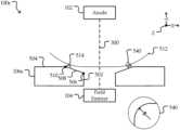
- FIG. 1is a block diagram of an x-ray tube according to some embodiments.
- the x-ray tube 100 aincludes an anode 102 , a field emitter 104 , and a focus electrode 106 a .
- the anode 102includes a structure configured to generate x-rays in response to incident electrons.
- the field emitter 104is configured to generate an electron beam that may be directed towards the anode 102 .
- the field emitter 104may include a variety of types of emitters.
- the field emitter 104may include a nanotube emitter, a nanowire emitter, a Spindt array, or the like.
- nanotubeshave at least a portion of the structure that has a hollow center, where nanowires or nanorods has a substantially solid core.
- nanotubealso refers to nanowire and nanorod.
- a nanotuberefers to a nanometer-scale (nm-scale) tube-like structure with an aspect ratio of at least 100:1 (length:width or diameter).
- a Spindt arraymay include individual field emitters with small sharp cones using an electron generating material, such as molybdenum (Mo) or Tungsten (W).
- the field emitter 104is formed of an electrically conductive or semi-conductive material with a high tensile strength and high thermal conductivity such as carbon, metal oxides (e.g., Al 2 O 3 , titanium oxide (TiO 2 ), zinc oxide (ZnO), or manganese oxide (Mn x O y , where x and y are integers)), metals, sulfides, nitrides, and carbides, either in pure or in doped form, or the like.
- metal oxidese.g., Al 2 O 3 , titanium oxide (TiO 2 ), zinc oxide (ZnO), or manganese oxide (Mn x O y , where x and y are integers
- the field emitter 104may include multiple field emitters.
- the field emitter 104may include, tens to hundreds or more of individual field emitters 104 .
- Each field emitter 104may be configured to generate an electron beam directed towards the anode 102 .
- Each field emitter 104may be associated with corresponding focus electrodes 106 , such as the focus electrodes pair 106 a , 106 shown in FIG. 1 , or a corresponding opening of a unitary focus electrode 106 .
- Field emitters 104may have areas that are larger relative to other types of emitters.
- a field emitter 104may have length of about 10 millimeters (mm) to about 30 mm and a width from about 2 mm to about 6 mm. In an example, the length of the field emitter 104 is at least 5 times larger than the width.
- the larger relative areamay result in a larger size of a focal spot on the anode 102 . Heating of the anode 102 due to incident electrons on the focal spot may be spread over that larger area, decreasing the thermal stress on the anode 102 , permitting a higher electron flux, or the like.
- field emitters 104may have a relatively lower current flux as compared to other emitters.
- the area of the field emitter 104may be increased. These aspects lead to larger relative areas for field emitters 104 .
- the larger relative areameans that the local field strength around the field emitter 104 is more sensitive to the anode 102 or tube voltage.
- the larger relative area of a field emitter 104may increase a probability of an arc. As the area of the field emitter 104 increases, a relative position of another structure that may receive an arc is moved further away from the anode 102 , decreasing the electric field strength on those structures relative to the electric field strength at the field emitter 104 . As a result, a probability that an arc may occur at the field emitter 104 may increase.
- Field emitters 104may be more sensitive to arcing than other types of emitters, such as thermionic emitters, due to their structure. For example, field emitters 104 may include relatively small structures, such as a thin layer, that may be damaged by an arc.
- the field emitter 104may be larger in area due to its nature and due to a desired larger focal spot for distributed heating. However, that increased area increases the probability of arcing occurring on the field emitter 104 .
- the focus electrode 106 amay alleviate the increased probability of arcing occurring on the field emitter 104 . As a result, benefits of the larger area of a field emitter 104 may be realized while the probability of damage to the field emitter 104 due to arcing is reduced.
- the focus electrode 106 ais disposed between the anode 102 and the field emitter 104 .
- the focus electrode 106 ais configured to adjust the size and/or shape of the focal spot on the anode 102 . At least part of the focus electrode 106 a is closer to the anode 102 than any part of the field emitter 104 .
- a shortest distance between any part of the field emitter 104 and any part of the anode 102may be distance 108 .
- a shortest distance from part of the focus electrode 106 a to the anode 102may be distance 110 .
- Distance 110is less than distance 108 .
- the focus electrode 106 ais disposed relative to the field emitter 104 and the anode 102 and shaped such that during operation, a point of highest electric field strength on a cathode structure is closer to the focus electrode 106 a than the field emitter 104 .
- the cathode structuremay include structures that are at or near the potential of the field emitter 104 .
- the anode 102may be at about 10-50 kilovolts (kV), about 50-150 kV, about 50-450 kV or the like (relative to the cathode structure or ground).
- these voltagesmay be associated with particular applications, such as mammography, medical diagnostic imaging, industrial imaging, explosive detection, non-destructive testing (NDT), or the like.
- the cathode structuresuch as the field emitter 104 , the focus electrode 106 a , a grid (not illustrated), or the like may be at voltages from about ⁇ 3 kV to about 1 kV.
- a higher electric field strengthmay increase the probability of an arc.
- the design of an x-ray tube 100 amay include minimizing local electric field strength maxima.
- the point of highest electric field strengthcan be created by design and, in particular, offset or shifted away from the field emitter 104 .
- the electric field strength at the point of highest electric field strengthmay be greater than about 8 times the highest electric field strength on the field emitter 104 .
- the structure of the focus electrode 106 amay result in the electric field strength at the point of highest electric field strength being at least about 25% higher than the electric field strength on a portion of the focus electrode 106 a closest to the field emitter 104 .
- FIG. 2is a block diagram of an x-ray system according to some embodiments.
- the x-ray system 200may include an x-ray tube 100 b similar to x-ray tube 100 a described above.
- the x-ray tube 100 bmay include a vacuum enclosure 212 where the anode 102 , field emitter 104 , and the focus electrode 106 b are disposed in an interior 202 a of the vacuum enclosure 212 .
- the x-ray system 200may include a voltage source 204 disposed on an exterior 202 b of the vacuum enclosure 212 .
- the voltage source 204may be configured to generate multiple voltages for the x-ray system 200 .
- the voltage source 204may be configured to generate one or more voltages 206 for the field emitter 104 , a high voltage 208 for the anode 102 , a focus electrode voltage 210 for the focus electrode 106 , or the like.
- the focus electrode 106 bmay be grounded. That is the focus electrode volage 210 may be 0 V or near 0 V. Portions of the vacuum enclosure 212 , a housing for the x-ray tube 100 b , or the like may be grounded. The focus electrode 106 b may share that ground. In some embodiments, the voltage source 204 may share that ground. As a result, arcs that discharge through the focus electrode 106 b may direct the charge to ground.
- the focus electrode 106 bmay be at a voltage 210 different from ground.
- the voltage source 204may be configured to apply a variable voltage to the focus electrode 106 b .
- the voltage source 204may include spark gap protectors or other circuitry to allow for the desired variability in the focus electrode voltage 210 while still accommodating arcs that may occur.
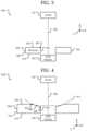
- FIG. 3is a block diagram of an x-ray tube with a two surface electrode according to some embodiments, where two surfaces 302 , 306 of the focus electrode have a higher electric field strength than two other surfaces 308 , 310 that face away from the anode.
- the x-ray tube 100 cmay be similar to the x-ray tubes 100 a - b . However, the focus electrode 106 c may have a particular structure.
- the focus electrode 106 cmay have a structure relative to an axis 300 .
- the field emitter 104 and the anode 102may form the axis 300 .
- the axis 300may be aligned in the general direction of the electrons emitted from the field emitter 104 traveling towards the anode 102 .
- the axis 300may extend along the Y axis.
- a component that extends axially relative to the axis 300may have some component along the Y axis.
- an axially extending componentmay extend only axially or only along the Y axis while other axially extending components may have some part that extends radially, i.e., perpendicular to the axis 300 or the Y axis parallel to the X-Z plane, extends along the X axis, extends along the Z axis, or the like.
- the focus electrode 106 cincludes at least two surfaces.
- two surfaces 302 and 304are used as an example.
- the first surface (or field emitter perpendicular surface or beam shaping surface) 302extends substantially parallel to the axis 300 or an emission surface of the field emitter 104 .
- the surface 302may include the beam shaping surface with a structure that shapes a focal spot on the anode 102 when operating.
- the surface 302may contribute to a majority of the shaping of the electric field to focus electrons from the field emitter 104 on the anode 102 .
- Other surfaces, such as surface 304may have some impact, but the relative contribution of surface 304 is less than that of surface 302 .
- the second surface (or anode facing parallel surface) 304 of the focus electrode 106 cextends radially away from the first surface 302 from the axis.
- the second surface 304is formed to extend only radially away parallel to the X-Z plane from the first surface 302 without a substantial axial component.
- the location 306 where the first surface 302 and the second surface joinmay be about a 90 degree angle.
- the second surface 304may be a surface that is nearest to the anode 102 . During operation, a point of highest electric field strength is disposed where the first surface 302 joins the second surface 304 .
- an electric field strength along surface 302may be necessarily less than that of the location 306 where the first surface 302 and the second surface 304 join.
- the relatively sharp feature of the location 306may increase the local electric field strength, as electric fields concentrate around the corners or edges of conductors in the field. As a result, an arc that may occur can have an increased probability of occurring at location 306 rather than on the field emitter 104 .
- the anglemay be different.
- the anglemay be larger or smaller in a range such that a local maximum of electric field strength on cathode structures occurs at the location 306 .
- FIG. 4is a block diagram of an x-ray tube with a three surface electrode according to some embodiments, where three surfaces 402 , 404 , 406 of the focus electrode have a higher electric field strength than other surfaces 414 , 416 that face away from the anode.
- the x-ray tube 100 dmay be similar to the x-ray tubes 100 a - c .
- the focus electrode 106may include at least three surfaces with a higher electric field strength.
- a first surface (or field emitter perpendicular surface or beam shaping surface) 402may be similar to the first surface 302 of focus electrode 106 c of x-ray tube 100 c .
- the first surface 402may be a beam shaping surface that affects the focal spot.
- a third surface (or anode facing surface) 408may extend radially parallel to the X-Z plane away from the first surface 402 and is joined to the first surface 402 at location (or inner angle or inner corner) 406 similar to the second surface 304 of focus electrode 106 c .
- the third surface 408also extends axially away from the first surface 402 relative to the axis 300 along the Y axis.
- the axial extension of the third surface 408is in a direction towards the anode.
- the angle of the first surface 402 and the third surface 408 at location 406may be greater than 90 degrees. If the angle at location 406 is greater, the electric field strength at location 406 may be reduced relative to an angle of 90 degrees.
- the third surface 408is a beam shaping surface and helps to shape the electron beam to a desired cross section with a desired trajectory on a focal spot on the anode 102 when operating.
- the focus electrodeincludes a second surface (or anode facing parallel surface) 404 .
- the second surface 404joins the third surface 408 at location (or outer angle or outer corner) 410 .
- the second surface 404extends away from the third surface 408 relative to the axis 300 .
- the resulting structureallows for both control of the focal spot through surface 402 , but also positioning of a point of higher electric field strength further away from the field emitter 104 by the angle at location 406 , the length of the third surface 404 , and the angle at location 410 .
- line 412is a point equidistant from the anode 102 .
- Location 410 where the third surface 408 joints the second surface 404may be at the equidistant line 412 .
- the location 406may be further from the anode 102 than the equidistant line 412 .
- an electric field strength at the location 406may be lower than the electric field strength at the location 410 .
- a point of highest electric field strengthmay be disposed at location 410 where the third surface 408 joins the second surface 404 .
- the angle of the second surface 404 to the third surface 408 at location 410may be determined such that other points along the second surface 404 are further from the anode 102 than the point 410 .
- an electric field strength along the surface 404may be less than the electric field strength at the location 410 .
- the electric field strength along the focus electrode 106 dmay be a local maximum at the location 410 . Any arcing may occur at the location 410 , rather than other locations along the focus electrode 106 d including those closer to the field emitter 104 . Due to the close proximity of location 306 ( FIG.
- arcing at the highest electric field strength location 306may still leak or arc to surrounding features, such as the field emitter 104 causing damage to the field emitter 104 .
- Moving the highest electric field strength to the location 410 ( FIG. 4 ) away from the field emitter 104reduces the likelihood that arcing at the highest electric field strength location 410 will leak or arc to the field emitter 104 , thus reducing the likelihood of damage to the field emitter 104 due to arcing.
- the location 306( FIG.
- the focus electrodes 106 ccan have improved beam shaping and focusing characteristics but with an increased likelihood of arcs and damage to the cathode structures, such as field emitters 104 , caused by arcs.
- the part or location (e.g., 410 ) of the focus electrode 106 d that is closer to the anode 102 (e.g., with the highest electric field strength) than any part of the field emitter 104is further from a center of the field emitter 104 than another part of the focus electrode 106 d (e.g., 402 , 406 , 408 ).
- beam shaping surfaces of the focus electrode 106 dsuch as surface 402 that face the electron beam, may be closer to a center of the field emitter 104 than that part or location (e.g., 410 ) of the focus electrode 106 d (with the highest electric field strength).
- the electric field strengthwill be higher at the part or location (e.g., 410 ) of the focus electrode 106 d that is closer to the anode 102 than the beam shaping surfaces (e.g., 402 , 404 , 408 ).
- FIG. 5is a block diagram of an x-ray tube with a focus electrode having a protrusion according to some embodiments.
- the x-ray tube 100 emay be similar to the x-ray tubes 100 a - d described above.
- the focus electrode 106 emay include surfaces 502 , 504 , and 508 with corresponding locations 506 and 510 similar to surfaces 402 , 404 , and 408 and locations 406 and 410 .
- the focus electrode 106 eincludes a protrusion 514 .
- the protrusionextends from the third surface 508 towards the anode 102 .
- the protrusion 514includes the part of the focus electrode 106 e that is closer to the anode 102 than any part of the field emitter 104 .
- Part of the protrusion 514is at the equidistant line 512 from the anode 102 . All other parts of the focus electrode 106 e are further from the anode 102 than that part of the protrusion 514 .
- the protrusion 514is associated with a local minimum radius. As the radius R, shown in view 540 , on a corner of the protrusion 514 decreases, the particular feature becomes sharper. The local radius R may approach zero or approach a sharp corner. With sharper features, smaller radii, or the like, the electric field may be more concentrated in that region.
- the protrusion 514may be offset from portions of the focus electrode 106 e that are closer to the field emitter 104 . As a result, the location of a higher electric field strength may be offset from the field emitter 104 .
- the location of the protrusion 514provides control over the location of a higher electric field strength and hence, the location where an arc may occur.
- the protrusion 514may be disposed at or closer to the location 510 than the location 506 .
- the protrusion 514where an arc may be more likely to occur, may be further away from the field emitter 104 .
- points across the third surface 508 other than the protrusion 514are substantially equidistant from the anode 102 .
- an electric field strength along those pointsmay be substantially the same.
- the electric field strength at the protrusion 514may necessarily be higher.
- focus electrode 106 ethat is similar to the focus electrode 106 d has been used as an example of a focus electrode 106 including a protrusion 514
- other focus electrodes 106may include a protrusion 514
- the focus electrode 106 emay include a structure similar to focus electrode 106 c of FIG. 3 but have a protrusion 514 that extends towards the anode 102 from a surface of the focus electrode 106 e.
- FIG. 6is a cutaway view of a focus electrode according to some embodiments.
- the focus electrode 106 fincludes multiple openings 620 .
- Each opening 620is associated with one of the multiple field emitters 104 .
- some point of the focus electrode 106 fis closer to the anode 102 than that field emitter 104 .
- the opening 620may have s first surface 602 similar to the first surfaces 302 , 402 , 502 , or the like, described above.
- the focus electrode 106 fmay include a second surface 604 similar to the second surfaces 304 , 404 , and 504 described above.
- each opening 620may be associated with multiple field emitters.
- the focus electrode 106 fmay still have a point that is closer to the anode, such as the anode 102 of FIGS. 1 - 5 , than any of those field emitters 104 .
- FIG. 7is a cutaway view of a focus electrode for multiple field emitters according to some embodiments.
- the focus electrode 106 gincludes a single opening 702 formed between portions 106 g - 1 and 106 g - 2 . Multiple field emitters 104 are disposed in the single opening 702 .
- a frame 704may be disposed between the field emitters 104 .
- the frame 704may be grounded or at the same potential as the focus electrode 106 g .
- the focus electrode 106 gmay have a cross-section similar to the focus electrodes 106 described above.
- the focus electrode 106 gmay have a cross-section, may include protrusions, or the like similar to focus electrodes 106 a - e described above.
- FIG. 8is a cross-sectional view of a cathode assembly including a focus electrode according to some embodiments.
- the cathode assembly 800includes a substrate 830 .
- the substrate 830may include a ceramic substrate or other insulating substrate.
- a conductive layer 836such as a copper layer is disposed on the substrate 830 .
- An emitter 844such as carbon nanotubes, nanowires, nanorods, or the like as described above may be disposed on the conductive layer 836 . Although one emitter 844 is illustrated, multiple emitters 844 may be present similar to field emitters 104 of FIG. 7 .
- a grid 834may be disposed over the emitter 844 .
- a voltagemay be applied between the conductive layer 836 and the grid 834 to generate electrons from the emitter 844 .
- the grid 834can be an intercepting type, where the electrons pass through the grid, such a mesh, as illustrated, or the grid can be a non-intercepting type (not shown), where the electrons pass through an open aperture.
- a frame 838 similar to the frame 704 of FIG. 7may be disposed on the substrate 830 .
- the frame 838may also contribute to the focusing of an electron beam.
- the frame 838may provide structural support for other components, such as the grid 834 .
- a spacer(not shown may separate the frame 838 and the grid 834 , and the spacer may be conductive or insulating.
- the frame 838may include multiple openings 838 ′ associated with multiple emitters 844 .
- a spacer 840may separate the frame 838 and the substrate 830 .
- the spacer 840may be conductive or insulating.
- the frame 838may include conductive materials.
- a second spacer 842is disposed on the frame 838 .
- the second spacer 842may be conductive or insulating.
- a focus electrode 106 his disposed on the second spacer 842 .
- the focus electrode 106 hmay be similar to the focus electrodes 106 a - g described above.
- the focus electrodemay include a first portion 106 h - 1 and a second portion 106 h - 2 similar to the portions 106 g - 1 and 106 g - 2 of FIG. 7 .
- Multiple openings 838 ′may be disposed between the portions 106 h - 1 and 106 h - 2 .
- the portions 106 h - 1 and 106 h - 2may extend along the emitters 844 , for example parallel to the Z direction.
- the spacer 842may be insulating, in some embodiments, the spacer 842 may be conductive or omitted. Thus, the focus electrode 106 h and the frame 838 may be at the same potential.
- the grid 834 or the frame 838may provide some protection for the emitter 844 from damage due to arcs; however, due to the relatively close proximity of the grid 834 and the frame 838 to the emitter 844 and the high voltage potential of the arc, the protection may be minimal.
- the frame 838may be about 200 micrometers ( ⁇ m) away from the emitter 844 .
- the proximity to the emitters 838makes the frame 838 or an attached grid less able to mitigate damage from any molten metal or metal vapor caused by the arc.
- a material of the spacer 842 or other structuremay be damaged if an arc occurs near the frame 838 .
- moving a location where an arc may occur to further from the emitter 844 and the frame 838 on the focus electrode 106 hmay reduce damage that may occur to the emitter 844 , frame 838 , spacer 842 , or other similar structures due to an arc.
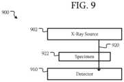
- FIG. 9is a block diagram of an x-ray imaging system according to some embodiments.
- the x-ray imaging system 900includes an x-ray source 902 and detector 910 .
- the x-ray source 902may be similar to an x-ray tube 100 a - e as described above.
- the x-ray source 902is disposed relative to the detector 910 such that x-rays 920 may be generated to pass through a specimen 922 and detected by the detector 910 .
- the detector 910is part of a medical imaging system, non-destructive testing system, or the like.
- the x-ray imaging system 900may include a portable vehicle scanning system as part of a cargo scanning system.
- Some embodimentsinclude an x-ray tube, comprising: a field emitter 104 including an emission surface; an anode 102 ; and a focus electrode 106 , 106 a - h disposed between the field emitter 104 and the anode 102 ; wherein: the focus electrode 106 , 106 a - h includes: a first surface 302 , 402 , 502 , 602 that is substantially perpendicular to the field emitter 104 emission surface and nearest to the field emitter 104 ; a second surface 304 , 404 , 504 , 604 that is axially nearest to the anode 102 , wherein the field emitter 104 and the anode 102 form an axis; and a third surface 308 , 408 , 508 that extends between the first surface 302 , 402 , 502 , 602 and the second surface 304 , 404 , 504 , 604 ; and a first location 406 , 50
- the second location 410 , 510 on the focus electrode 106 , 106 a - his further from a center of the field emitter 104 than another part of the focus electrode 106 , 106 a - h.
- the focus electrode 106 , 106 a - his grounded.
- the focus electrode 106 , 106 a - hfurther comprises a protrusion 514 extending towards the anode 102 .
- the protrusion 514is closer to the second location 410 , 510 on the focus electrode 106 , 106 a - h and the anode 102 than the first location 406 , 506 on the focus electrode 106 , 106 a - h.
- the focus electrode 106 , 106 a - his shaped such that during operation, a point of highest electric field strength is disposed at the second location 410 , 510 .
- the second surface 304 , 404 , 504 , 604extends radially and axially away from the first surface 302 , 402 , 502 , 602 relative to the axis.
- the x-ray tubefurther comprises: a cathode structure including: a substrate wherein the field emitter 104 is disposed on the substrate; a frame disposed on the substrate over the field emitter 104 ; and the focus electrode 106 , 106 a - h wherein the focus electrode 106 , 106 a - h is disposed on the frame.
- a cathode structureincluding: a substrate wherein the field emitter 104 is disposed on the substrate; a frame disposed on the substrate over the field emitter 104 ; and the focus electrode 106 , 106 a - h wherein the focus electrode 106 , 106 a - h is disposed on the frame.
- the field emitter 104is one a multiple field emitter 104 s disposed on the substrate; the frame includes multiple openings, each opening corresponding to one of the multiple field emitter 104 s ; the focus electrode 106 , 106 a - h includes a first portion and a second portion; and the openings of the frame are disposed between the first portion and the second portion.
- points across the second surface 304 , 404 , 504 , 604are substantially equidistant from the anode 102 .
- Some embodimentsinclude an x-ray tube, comprising: a cathode structure 800 including a field emitter 104 ; an anode 102 ; and a focus electrode 106 , 106 a - h disposed between the field emitter 104 and the anode 102 ; wherein the focus electrode 106 , 106 a - h is disposed relative to the field emitter 104 and the anode 102 , and the focus electrode 106 , 106 a - h is shaped such that during operation, a point of highest electric field strength on the cathode structure is closer to the focus electrode 106 , 106 a - h than the field emitter 104 .
- the point of highest electric field strengthis further from a center of the field emitter 104 than another part of the focus electrode 106 , 106 a - h.
- the focus electrode 106 , 106 a - his grounded.
- the field emitter 104 and the anode 102form an axis; and the focus electrode 106 , 106 a - h comprises: a first surface 302 , 402 , 502 , 602 extending substantially parallel to the axis; a second surface 304 , 404 , 504 , 604 extending radially away from the first surface 302 , 402 , 502 , 602 relative to the axis.
- a first location on the focus electrode 106 , 106 a - his between the first surface 302 , 402 , 502 , 602 and the second surface 304 , 404 , 504 , 604 ; and the focus electrode 106 , 106 a - h is shaped such that during operation, a point of highest electric field strength is disposed at the first location.
- the field emitter 104 and the anode 102form an axis; and the focus electrode 106 , 106 a - h comprises: a first surface 302 , 402 , 502 , 602 extending substantially parallel to the axis; a second surface 304 , 404 , 504 , 604 extending radially away from the first surface 302 , 402 , 502 , 602 relative to the axis; a third surface 308 , 408 , 508 extending radially and axially away from the first surface 302 , 402 , 502 , 602 relative to the axis towards the second surface 304 , 404 , 504 , 604 ; and a first location 306 , 406 , 506 on the focus electrode 106 , 106 a - h between the first surface 302 , 402 , 502 , 602 and the third surface 308 , 408 , 508 ; and a
- the focus electrode 106 , 106 a - his shaped such that during operation, a point of highest electric field strength is disposed at the second location 410 , 510 .
- points across the second surface 304 , 404 , 504 , 604are substantially equidistant from the anode 102 .
- Some embodimentsinclude an x-ray tube, comprising: means for emitting electrons towards an anode; and means for focusing electrons emitted from the means for emitting electrons towards the anode, comprising: means for increasing an electric field strength at the means for focusing electrons beyond an electric field strength at the means for emitting electrons.
- Examples of the means for emitting electrons towards an anodeinclude the cathode structure 800 , the field emitter 104 , the grid 834 , or the like.
- the means for emitting electrons towards an anodecan include at least three field emitters 104 .
- Examples of the means for focusing electrons emitted from the means for emitting electrons towards the anodeinclude the focus electrode 106 , 106 a - h , and the frame 704 , 838 .
- Examples of the means for increasing an electric field strength at the means for focusing electrons beyond an electric field strength at the means for emitting electronsinclude surfaces 302 , 402 , 502 , 602 , 408 , 508 , locations or edges 406 , 506 , the protrusion 514 , or the like
- the means for focusing electronsfurther comprises: means for positioning a point of maximum electric field strength on the means for focusing electrons further from the means for emitting electrons than a closest part of the means for focusing electrons to the means for emitting electrons.
- means for positioning a point of maximum electric field strength on the means for focusing electrons further from the means for emitting electrons than a closest part of the means for focusing electrons to the means for emitting electronsinclude the location 410 and 510 , the protrusion 514 , or the like.
- claim 4can depend from either of claims 1 and 3 , with these separate dependencies yielding two distinct embodiments; claim 5 can depend from any one of claim 1 , 3 , or 4 , with these separate dependencies yielding three distinct embodiments; claim 6 can depend from any one of claim 1 , 3 , 4 , or 5 , with these separate dependencies yielding four distinct embodiments; and so on.
Landscapes
- X-Ray Techniques (AREA)
Abstract
Description
Claims (20)
Priority Applications (5)
| Application Number | Priority Date | Filing Date | Title |
|---|---|---|---|
| US17/855,739US12230468B2 (en) | 2022-06-30 | 2022-06-30 | X-ray system with field emitters and arc protection |
| EP23181800.6AEP4300538A3 (en) | 2022-06-30 | 2023-06-27 | X-ray system with field emitters and arc protection |
| JP2023106567AJP2024007456A (en) | 2022-06-30 | 2023-06-29 | X-ray system with field emitter and arc protection |
| CN202310780589.0ACN117334546A (en) | 2022-06-30 | 2023-06-29 | X-ray system with field emitter and arc protection |
| AU2023204135AAU2023204135A1 (en) | 2022-06-30 | 2023-06-29 | X-ray system with field emitters and arc protection |
Applications Claiming Priority (1)
| Application Number | Priority Date | Filing Date | Title |
|---|---|---|---|
| US17/855,739US12230468B2 (en) | 2022-06-30 | 2022-06-30 | X-ray system with field emitters and arc protection |
Publications (2)
| Publication Number | Publication Date |
|---|---|
| US20240006144A1 US20240006144A1 (en) | 2024-01-04 |
| US12230468B2true US12230468B2 (en) | 2025-02-18 |
Family
ID=87002985
Family Applications (1)
| Application Number | Title | Priority Date | Filing Date |
|---|---|---|---|
| US17/855,739Active2042-12-01US12230468B2 (en) | 2022-06-30 | 2022-06-30 | X-ray system with field emitters and arc protection |
Country Status (5)
| Country | Link |
|---|---|
| US (1) | US12230468B2 (en) |
| EP (1) | EP4300538A3 (en) |
| JP (1) | JP2024007456A (en) |
| CN (1) | CN117334546A (en) |
| AU (1) | AU2023204135A1 (en) |
Families Citing this family (1)
| Publication number | Priority date | Publication date | Assignee | Title |
|---|---|---|---|---|
| US12230468B2 (en)* | 2022-06-30 | 2025-02-18 | Varex Imaging Corporation | X-ray system with field emitters and arc protection |
Citations (494)
| Publication number | Priority date | Publication date | Assignee | Title |
|---|---|---|---|---|
| USRE28544E (en) | 1971-07-07 | 1975-09-02 | Radiant energy imaging with scanning pencil beam | |
| US4203036A (en) | 1976-11-02 | 1980-05-13 | Siemens Aktiengesellschaft | X-ray diagnostic apparatus for producing transverse layer images |
| US4219733A (en) | 1977-04-01 | 1980-08-26 | Siemens Aktiengesellschaft | X-Ray diagnostic apparatus producing transverse layer images |
| US4274005A (en) | 1978-09-29 | 1981-06-16 | Tokyo Shibaura Denki Kabushiki Kaisha | X-ray apparatus for computed tomography scanner |
| US4592080A (en) | 1983-07-29 | 1986-05-27 | Siemens Aktiengesellschaft | Computer tomograph |
| US4606061A (en) | 1983-12-28 | 1986-08-12 | Tokyo Shibaura Denki Kabushiki Kaisha | Light controlled x-ray scanner |
| US4788705A (en) | 1984-12-20 | 1988-11-29 | Varian Assoicates, Inc. | High-intensity X-ray source |
| US4819256A (en) | 1987-04-20 | 1989-04-04 | American Science And Engineering, Inc. | Radiographic sensitivity for detection of flaws and cracks |
| US4821305A (en) | 1986-03-25 | 1989-04-11 | Varian Associates, Inc. | Photoelectric X-ray tube |
| US4857799A (en) | 1986-07-30 | 1989-08-15 | Sri International | Matrix-addressed flat panel display |
| US4877554A (en) | 1987-07-22 | 1989-10-31 | Murata Manufacturing Co., Ltd. | Resistance paste |
| US4914681A (en) | 1986-11-25 | 1990-04-03 | Siemens Aktiengesellschaft | Computer tomography apparatus |
| US5015912A (en) | 1986-07-30 | 1991-05-14 | Sri International | Matrix-addressed flat panel display |
| US5022062A (en) | 1989-09-13 | 1991-06-04 | American Science And Engineering, Inc. | Automatic threat detection based on illumination by penetrating radiant energy using histogram processing |
| USRE33634E (en) | 1986-09-23 | 1991-07-09 | Method and structure for optimizing radiographic quality by controlling X-ray tube voltage, current focal spot size and exposure time | |
| US5125012A (en) | 1990-07-18 | 1992-06-23 | Siemens Aktiengesellschaft | Computer tomography apparatus |
| US5149584A (en) | 1990-10-23 | 1992-09-22 | Baker R Terry K | Carbon fiber structures having improved interlaminar properties |
| US5150394A (en) | 1989-12-05 | 1992-09-22 | University Of Massachusetts Medical School | Dual-energy system for quantitative radiographic imaging |
| US5153900A (en) | 1990-09-05 | 1992-10-06 | Photoelectron Corporation | Miniaturized low power x-ray source |
| US5164972A (en) | 1990-10-15 | 1992-11-17 | Siemens Aktiengesellschaft | Computer tomography apparatus having an annularly guided electron beam |
| US5179581A (en) | 1989-09-13 | 1993-01-12 | American Science And Engineering, Inc. | Automatic threat detection based on illumination by penetrating radiant energy |
| US5179583A (en) | 1990-04-30 | 1993-01-12 | Shimadzu Corporation | X-ray tube for ct apparatus |
| US5181234A (en) | 1990-08-06 | 1993-01-19 | Irt Corporation | X-ray backscatter detection system |
| US5191600A (en) | 1990-05-11 | 1993-03-02 | Bruker Analytic | X-ray computer tomography system with split detector ring |
| US5193105A (en) | 1991-12-18 | 1993-03-09 | Imatron, Inc. | Ion controlling electrode assembly for a scanning electron beam computed tomography scanner |
| US5195112A (en) | 1990-05-11 | 1993-03-16 | Bruker Analytic | X-ray computer tomography system |
| US5200985A (en) | 1992-01-06 | 1993-04-06 | Picker International, Inc. | X-ray tube with capacitively coupled filament drive |
| US5241577A (en) | 1992-01-06 | 1993-08-31 | Picker International, Inc. | X-ray tube with bearing slip ring |
| US5243252A (en) | 1989-12-19 | 1993-09-07 | Matsushita Electric Industrial Co., Ltd. | Electron field emission device |
| US5247556A (en) | 1991-02-06 | 1993-09-21 | Siemens Aktiengesellschaft | Method and apparatus of operating a computer tomography apparatus to simultaneously obtain an x-ray shadowgraph and a tomographic exposure |
| US5268955A (en) | 1992-01-06 | 1993-12-07 | Picker International, Inc. | Ring tube x-ray source |
| US5274690A (en) | 1992-01-06 | 1993-12-28 | Picker International, Inc. | Rotating housing and anode/stationary cathode x-ray tube with magnetic susceptor for holding the cathode stationary |
| US5291538A (en) | 1992-01-06 | 1994-03-01 | Picker International. Inc. | X-ray tube with ferrite core filament transformer |
| US5305363A (en) | 1992-01-06 | 1994-04-19 | Picker International, Inc. | Computerized tomographic scanner having a toroidal x-ray tube with a stationary annular anode and a rotating cathode assembly |
| US5313511A (en) | 1986-06-20 | 1994-05-17 | American Science And Engineering, Inc. | X-ray imaging particularly adapted for low Z materials |
| WO1994015350A1 (en) | 1992-12-23 | 1994-07-07 | Microelectronics And Computer Technology Corporation | Diode structure flat panel display |
| WO1994015352A1 (en) | 1992-12-23 | 1994-07-07 | Microelectronics And Computer Technology Corporation | Triode structure flat panel display employing flat field emission cathodes |
| WO1994028571A1 (en) | 1993-06-02 | 1994-12-08 | Microelectronics And Computer Technology Corporation | Amorphic diamond film flat field emission cathode |
| US5378408A (en) | 1993-07-29 | 1995-01-03 | E. I. Du Pont De Nemours And Company | Lead-free thick film paste composition |
| US5384820A (en) | 1992-01-06 | 1995-01-24 | Picker International, Inc. | Journal bearing and radiation shield for rotating housing and anode/stationary cathode X-ray tubes |
| US5413866A (en) | 1990-10-23 | 1995-05-09 | Baker; R. Terry K. | High performance carbon filament structures |
| US5438605A (en) | 1992-01-06 | 1995-08-01 | Picker International, Inc. | Ring tube x-ray source with active vacuum pumping |
| US5458784A (en) | 1990-10-23 | 1995-10-17 | Catalytic Materials Limited | Removal of contaminants from aqueous and gaseous streams using graphic filaments |
| US5475729A (en) | 1994-04-08 | 1995-12-12 | Picker International, Inc. | X-ray reference channel and x-ray control circuit for ring tube CT scanners |
| US5493599A (en) | 1992-04-03 | 1996-02-20 | Picker International, Inc. | Off-focal radiation limiting precollimator and adjustable ring collimator for x-ray CT scanners |
| US5504791A (en) | 1994-03-18 | 1996-04-02 | Siemens Aktiengesellschaft | Annular anode x-ray computed tomography apparatus with a single magnet system for guiding and deflecting the electron beam |
| US5548630A (en) | 1994-09-16 | 1996-08-20 | Siemens Aktiengesellschaft | X-ray radiator having an electron source for sending a beam of electrons along an elongated anode |
| US5567357A (en) | 1993-08-25 | 1996-10-22 | Tatsuta Electric Wire & Cable Co., Ltd. | Conductive paint having good adhesion to molding of metallic oxide |
| US5581591A (en) | 1992-01-06 | 1996-12-03 | Picker International, Inc. | Focal spot motion control for rotating housing and anode/stationary cathode X-ray tubes |
| US5591312A (en) | 1992-10-09 | 1997-01-07 | William Marsh Rice University | Process for making fullerene fibers |
| US5618875A (en) | 1990-10-23 | 1997-04-08 | Catalytic Materials Limited | High performance carbon filament structures |
| US5642394A (en) | 1996-04-03 | 1997-06-24 | American Science And Engineering, Inc. | Sidescatter X-ray detection system |
| US5644612A (en) | 1993-01-25 | 1997-07-01 | Cardiac Mariners, Inc. | Image reconstruction methods |
| US5726524A (en) | 1996-05-31 | 1998-03-10 | Minnesota Mining And Manufacturing Company | Field emission device having nanostructured emitters |
| US5729583A (en) | 1995-09-29 | 1998-03-17 | The United States Of America As Represented By The Secretary Of Commerce | Miniature x-ray source |
| US5748701A (en)* | 1994-08-29 | 1998-05-05 | Siemens Aktiengesellschaft | Cathode system for an X-ray tube |
| US5763886A (en) | 1996-08-07 | 1998-06-09 | Northrop Grumman Corporation | Two-dimensional imaging backscatter probe |
| US5764683A (en) | 1996-02-12 | 1998-06-09 | American Science And Engineering, Inc. | Mobile X-ray inspection system for large objects |
| US5768337A (en) | 1996-07-30 | 1998-06-16 | Varian Associates, Inc. | Photoelectric X-ray tube with gain |
| US5773921A (en) | 1994-02-23 | 1998-06-30 | Keesmann; Till | Field emission cathode having an electrically conducting material shaped of a narrow rod or knife edge |
| US5854822A (en) | 1997-07-25 | 1998-12-29 | Xrt Corp. | Miniature x-ray device having cold cathode |
| US5864146A (en) | 1996-11-13 | 1999-01-26 | University Of Massachusetts Medical Center | System for quantitative radiographic imaging |
| US5869922A (en) | 1997-08-13 | 1999-02-09 | Si Diamond Technology, Inc. | Carbon film for field emission devices |
| US5892231A (en) | 1997-02-05 | 1999-04-06 | Lockheed Martin Energy Research Corporation | Virtual mask digital electron beam lithography |
| WO1999031702A1 (en) | 1997-12-15 | 1999-06-24 | E.I. Du Pont De Nemours And Company | Ion bombarded graphite electron emitters |
| US5977697A (en) | 1994-12-22 | 1999-11-02 | Lucent Technologies Inc. | Field emission devices employing diamond particle emitters |
| US5995586A (en) | 1997-03-12 | 1999-11-30 | Siemens Aktiengesellschaft | X-ray generator |
| US6009141A (en) | 1997-05-26 | 1999-12-28 | Siemens Aktiengesellschaft | X-ray computed tomography apparatus with electronic scanning of a ring-shaped anode |
| US6018562A (en) | 1995-11-13 | 2000-01-25 | The United States Of America As Represented By The Secretary Of The Army | Apparatus and method for automatic recognition of concealed objects using multiple energy computed tomography |
| US6019656A (en) | 1997-11-29 | 2000-02-01 | Electronics And Telecommunications Research Institute | Method of fabricating a field emission device by using carbon nano-tubes |
| US6031892A (en) | 1989-12-05 | 2000-02-29 | University Of Massachusetts Medical Center | System for quantitative radiographic imaging |
| US6057637A (en) | 1996-09-13 | 2000-05-02 | The Regents Of The University Of California | Field emission electron source |
| US6074893A (en) | 1993-09-27 | 2000-06-13 | Sumitomo Metal Industries, Ltd. | Process for forming fine thick-film conductor patterns |
| EP1020888A1 (en) | 1999-01-11 | 2000-07-19 | Matsushita Electronics Corporation | Carbon ink, electron-emitting element, method for manufacturing an electron-emitting element and image display device |
| US6094472A (en) | 1998-04-14 | 2000-07-25 | Rapiscan Security Products, Inc. | X-ray backscatter imaging system including moving body tracking assembly |
| US6097138A (en) | 1996-09-18 | 2000-08-01 | Kabushiki Kaisha Toshiba | Field emission cold-cathode device |
| US6118852A (en) | 1998-07-02 | 2000-09-12 | General Electric Company | Aluminum x-ray transmissive window for an x-ray tube vacuum vessel |
| US6146230A (en) | 1998-09-24 | 2000-11-14 | Samsung Display Devices Co., Ltd. | Composition for electron emitter of field emission display and method for producing electron emitter using the same |
| US6156433A (en) | 1996-01-26 | 2000-12-05 | Dai Nippon Printing Co., Ltd. | Electrode for plasma display panel and process for producing the same |
| US6181765B1 (en) | 1998-12-10 | 2001-01-30 | General Electric Company | X-ray tube assembly |
| US6195411B1 (en) | 1999-05-13 | 2001-02-27 | Photoelectron Corporation | Miniature x-ray source with flexible probe |
| US6225225B1 (en) | 1999-09-09 | 2001-05-01 | Chartered Semiconductor Manufacturing Ltd. | Method to form shallow trench isolation structures for borderless contacts in an integrated circuit |
| US6236709B1 (en) | 1998-05-04 | 2001-05-22 | Ensco, Inc. | Continuous high speed tomographic imaging system and method |
| US6239547B1 (en) | 1997-09-30 | 2001-05-29 | Ise Electronics Corporation | Electron-emitting source and method of manufacturing the same |
| US6250984B1 (en) | 1999-01-25 | 2001-06-26 | Agere Systems Guardian Corp. | Article comprising enhanced nanotube emitter structure and process for fabricating article |
| US6252925B1 (en) | 1997-08-04 | 2001-06-26 | General Electric Company | System and method for performing computed tomography with fiber waveguides |
| US6259765B1 (en) | 1997-06-13 | 2001-07-10 | Commissariat A L'energie Atomique | X-ray tube comprising an electron source with microtips and magnetic guiding means |
| US20010009970A1 (en) | 1995-08-24 | 2001-07-26 | Medtronic Ave, Inc. | X-ray catheter |
| US6277318B1 (en) | 1999-08-18 | 2001-08-21 | Agere Systems Guardian Corp. | Method for fabrication of patterned carbon nanotube films |
| US6282260B1 (en) | 1998-12-14 | 2001-08-28 | American Science & Engineering, Inc. | Unilateral hand-held x-ray inspection apparatus |
| US6280697B1 (en) | 1999-03-01 | 2001-08-28 | The University Of North Carolina-Chapel Hill | Nanotube-based high energy material and method |
| US20010025962A1 (en) | 2000-03-31 | 2001-10-04 | Masayuki Nakamoto | Field emmision type cold cathode device, manufacturing method thereof and vacuum micro device |
| US6312303B1 (en) | 1999-07-19 | 2001-11-06 | Si Diamond Technology, Inc. | Alignment of carbon nanotubes |
| US6320933B1 (en) | 1998-11-30 | 2001-11-20 | American Science And Engineering, Inc. | Multiple scatter system for threat identification |
| WO2001093292A1 (en) | 2000-05-26 | 2001-12-06 | E.I. Dupont De Nemours And Company | Catalytically grown carbon fiber field emitters and field emitter cathodes made therefrom |
| US6331194B1 (en) | 1996-06-25 | 2001-12-18 | The United States Of America As Represented By The United States Department Of Energy | Process for manufacturing hollow fused-silica insulator cylinder |
| US6333444B1 (en) | 1999-04-01 | 2001-12-25 | Bp Chemicals Limited | Oxidation catalyst and process utilizing the catalyst |
| US6333968B1 (en) | 2000-05-05 | 2001-12-25 | The United States Of America As Represented By The Secretary Of The Navy | Transmission cathode for X-ray production |
| US6334939B1 (en) | 2000-06-15 | 2002-01-01 | The University Of North Carolina At Chapel Hill | Nanostructure-based high energy capacity material |
| US20020006489A1 (en) | 2000-07-07 | 2002-01-17 | Yoshitaka Goth | Electron emitter, manufacturing method thereof and electron beam device |
| US6356570B1 (en) | 1997-12-12 | 2002-03-12 | Technion Research And Development Foundation Ltd | Source of intense coherent high frequency radiation |
| US6359383B1 (en) | 1999-08-19 | 2002-03-19 | Industrial Technology Research Institute | Field emission display device equipped with nanotube emitters and method for fabricating |
| US6379745B1 (en) | 1997-02-20 | 2002-04-30 | Parelec, Inc. | Low temperature method and compositions for producing electrical conductors |
| US6385292B1 (en) | 2000-12-29 | 2002-05-07 | Ge Medical Systems Global Technology Company, Llc | Solid-state CT system and method |
| WO2002041348A1 (en) | 2000-11-20 | 2002-05-23 | Nec Corporation | Cnt film and field-emission cold cathode comprising the same |
| US20020063500A1 (en) | 2000-11-30 | 2002-05-30 | Medirad I.R.T. Ltd. | Miniature X-ray tube constructions |
| US20020074932A1 (en) | 2000-06-21 | 2002-06-20 | Bouchard Robert Joseph | Process for improving the emission of electron field emitters |
| US6409567B1 (en) | 1997-12-15 | 2002-06-25 | E.I. Du Pont De Nemours And Company | Past-deposited carbon electron emitters |
| US20020085674A1 (en) | 2000-12-29 | 2002-07-04 | Price John Scott | Radiography device with flat panel X-ray source |
| US6424695B1 (en) | 1998-12-22 | 2002-07-23 | American Science And Engineering, Inc. | Separate lateral processing of backscatter signals |
| US6436221B1 (en) | 2001-02-07 | 2002-08-20 | Industrial Technology Research Institute | Method of improving field emission efficiency for fabricating carbon nanotube field emitters |
| US6440761B1 (en) | 1999-05-24 | 2002-08-27 | Samsung Sdi Co., Ltd. | Carbon nanotube field emission array and method for fabricating the same |
| US6456691B2 (en) | 2000-03-06 | 2002-09-24 | Rigaku Corporation | X-ray generator |
| US6473487B1 (en) | 2000-12-27 | 2002-10-29 | Rapiscan Security Products, Inc. | Method and apparatus for physical characteristics discrimination of objects using a limited view three dimensional reconstruction |
| US20020189400A1 (en) | 1998-02-24 | 2002-12-19 | Kodas Toivo T. | Metal-carbon composite powders |
| US20030002627A1 (en) | 2000-09-28 | 2003-01-02 | Oxford Instruments, Inc. | Cold emitter x-ray tube incorporating a nanostructured carbon film electron emitter |
| US20030002628A1 (en)* | 2001-06-27 | 2003-01-02 | Wilson Colin R. | Method and system for generating an electron beam in x-ray generating devices |
| US6504292B1 (en) | 1999-07-15 | 2003-01-07 | Agere Systems Inc. | Field emitting device comprising metallized nanostructures and method for making the same |
| US20030023592A1 (en) | 2001-07-27 | 2003-01-30 | Rapiscan Security Products (Usa), Inc. | Method and system for certifying operators of x-ray inspection systems |
| US6542580B1 (en) | 2002-01-15 | 2003-04-01 | Rapiscan Security Products (Usa), Inc. | Relocatable X-ray imaging system and method for inspecting vehicles and containers |
| US6553096B1 (en) | 2000-10-06 | 2003-04-22 | The University Of North Carolina Chapel Hill | X-ray generating mechanism using electron field emission cathode |
| US20030092207A1 (en) | 2001-10-19 | 2003-05-15 | Zvi Yaniv | Activation effect on carbon nanotubes |
| US6597760B2 (en) | 2001-05-23 | 2003-07-22 | Heimann Systems Gmbh | Inspection device |
| US6616497B1 (en) | 1999-08-12 | 2003-09-09 | Samsung Sdi Co., Ltd. | Method of manufacturing carbon nanotube field emitter by electrophoretic deposition |
| US6630772B1 (en) | 1998-09-21 | 2003-10-07 | Agere Systems Inc. | Device comprising carbon nanotube field emitter structure and process for forming device |
| WO2003084865A2 (en) | 2001-06-14 | 2003-10-16 | Hyperion Catalysis International, Inc. | Field emission devices using modified carbon nanotubes |
| US6646382B2 (en) | 2001-09-19 | 2003-11-11 | Aet Japan, Inc. | Microminiature microwave electron source |
| US20030210764A1 (en) | 2002-05-10 | 2003-11-13 | Tekletsadik Kasegn Dubale | Pulsed power application for x-ray tube |
| US6653588B1 (en) | 1998-05-05 | 2003-11-25 | Rapiscan Security Products Limited | Auto reject unit |
| US6661875B2 (en) | 2002-05-09 | 2003-12-09 | Spire Corporation | Catheter tip x-ray source |
| US6661867B2 (en) | 2001-10-19 | 2003-12-09 | Control Screening, Llc | Tomographic scanning X-ray inspection system using transmitted and compton scattered radiation |
| US6661876B2 (en) | 2001-07-30 | 2003-12-09 | Moxtek, Inc. | Mobile miniature X-ray source |
| US6664722B1 (en) | 1999-12-02 | 2003-12-16 | Si Diamond Technology, Inc. | Field emission material |
| US6665373B1 (en) | 2002-03-12 | 2003-12-16 | Rapiscan Security Products (Usa), Inc. | X-ray imaging system with active detector |
| US6674837B1 (en) | 2001-06-15 | 2004-01-06 | Nan Crystal Imaging Corporation | X-ray imaging system incorporating pixelated X-ray source and synchronized detector |
| US20040013597A1 (en) | 2002-04-12 | 2004-01-22 | Si Diamond Technology, Inc. | Metallization of carbon nanotubes for field emission applications |
| US20040018371A1 (en) | 2002-04-12 | 2004-01-29 | Si Diamond Technology, Inc. | Metallization of carbon nanotubes for field emission applications |
| US20040025732A1 (en) | 2000-06-30 | 2004-02-12 | Tuck Richard Allan | Field electron emission materials and devices |
| US6718012B2 (en) | 2002-05-30 | 2004-04-06 | Moshe Ein-Gal | Electromagnetic wave energy emitter |
| US20040070326A1 (en) | 2002-10-09 | 2004-04-15 | Nano-Proprietary, Inc. | Enhanced field emission from carbon nanotubes mixed with particles |
| US6731716B2 (en) | 2001-02-23 | 2004-05-04 | Mitsubishi Heavy Industries, Ltd. | X-ray CT apparatus |
| US6741025B2 (en) | 1997-12-04 | 2004-05-25 | Printable Field Emitters Limited | Field electron emission materials with insulating material disposed in particular area and devices |
| US6739932B2 (en) | 2001-06-07 | 2004-05-25 | Si Diamond Technology, Inc. | Field emission display using carbon nanotubes and methods of making the same |
| WO2004049373A1 (en) | 2002-11-27 | 2004-06-10 | Sony Corporation | Method for manufacturing electron-emitting device and method for manufacturing display |
| US6760407B2 (en) | 2002-04-17 | 2004-07-06 | Ge Medical Global Technology Company, Llc | X-ray source and method having cathode with curved emission surface |
| US6763083B2 (en) | 2002-08-30 | 2004-07-13 | The United States Of America As Represented By The Administrator Of The National Aeronautics And Space Administration | Article screening system |
| US6768534B2 (en) | 2001-01-26 | 2004-07-27 | Sony Corporation | Display unit and method of manufacturing the display unit |
| USRE38561E1 (en) | 1995-02-22 | 2004-08-03 | Till Keesmann | Field emission cathode |
| US6785360B1 (en) | 2001-07-02 | 2004-08-31 | Martin Annis | Personnel inspection system with x-ray line source |
| US6787122B2 (en) | 2001-06-18 | 2004-09-07 | The University Of North Carolina At Chapel Hill | Method of making nanotube-based material with enhanced electron field emission properties |
| US20040191698A1 (en) | 2001-11-30 | 2004-09-30 | Takao Yagi | Manufacturing method of electron emitting member manufacturing method of cold cathode field emission device and manufacturing method of cold cathode field emission display |
| US20040198892A1 (en) | 2003-04-01 | 2004-10-07 | Cabot Microelectronics Corporation | Electron source and method for making same |
| US6807248B2 (en) | 2001-02-28 | 2004-10-19 | Mitsubishi Heavy Industries, Ltd. | Multisource type X-ray CT apparatus |
| US6806629B2 (en) | 2002-03-08 | 2004-10-19 | Chien-Min Sung | Amorphous diamond materials and associated methods for the use and manufacture thereof |
| US6809465B2 (en) | 2002-08-23 | 2004-10-26 | Samsung Electronics Co., Ltd. | Article comprising MEMS-based two-dimensional e-beam sources and method for making the same |
| US20040213378A1 (en) | 2003-04-24 | 2004-10-28 | The University Of North Carolina At Chapel Hill | Computed tomography system for imaging of human and small animal |
| US6812426B1 (en) | 2000-07-24 | 2004-11-02 | Rapiscan Security Products | Automatic reject unit spacer and diverter |
| US20040218714A1 (en) | 2003-04-30 | 2004-11-04 | Faust Anthony A. | Detection of explosive devices using X-ray backscatter radiation |
| US6815790B2 (en) | 2003-01-10 | 2004-11-09 | Rapiscan, Inc. | Position sensing detector for the detection of light within two dimensions |
| US20040224081A1 (en) | 2003-05-08 | 2004-11-11 | Industrial Technology Research Institute | Method for carbon nanotube emitter surface treatment |
| WO2004099068A2 (en) | 2003-05-05 | 2004-11-18 | Nanosys, Inc. | Nanofiber surfaces for use in enhanced surface area applications |
| WO2004102604A1 (en) | 2003-05-16 | 2004-11-25 | Koninklijke Philips Electronics N.V. | Field emission display and method of manufacturing the same |
| US20040240616A1 (en) | 2003-05-30 | 2004-12-02 | Applied Nanotechnologies, Inc. | Devices and methods for producing multiple X-ray beams from multiple locations |
| US20040256975A1 (en) | 2003-06-19 | 2004-12-23 | Applied Nanotechnologies, Inc. | Electrode and associated devices and methods |
| US6839403B1 (en) | 2000-07-24 | 2005-01-04 | Rapiscan Security Products (Usa), Inc. | Generation and distribution of annotation overlays of digital X-ray images for security systems |
| US6843599B2 (en) | 2002-07-23 | 2005-01-18 | Rapiscan, Inc. | Self-contained, portable inspection system and method |
| US20050025280A1 (en) | 2002-12-10 | 2005-02-03 | Robert Schulte | Volumetric 3D x-ray imaging system for baggage inspection including the detection of explosives |
| US6856667B2 (en) | 2001-04-03 | 2005-02-15 | L-3 Communications Security And Detection Systems Corporation Delaware | X-ray inspection system |
| US20050038498A1 (en) | 2003-04-17 | 2005-02-17 | Nanosys, Inc. | Medical device applications of nanostructured surfaces |
| US6858521B2 (en) | 2002-12-31 | 2005-02-22 | Samsung Electronics Co., Ltd. | Method for fabricating spaced-apart nanostructures |
| US6859518B2 (en) | 2002-11-19 | 2005-02-22 | Invision Technologies, Inc. | X-ray technique-based nonintrusive inspection apparatus |
| US6864162B2 (en) | 2002-08-23 | 2005-03-08 | Samsung Electronics Co., Ltd. | Article comprising gated field emission structures with centralized nanowires and method for making the same |
| US6876724B2 (en) | 2000-10-06 | 2005-04-05 | The University Of North Carolina - Chapel Hill | Large-area individually addressable multi-beam x-ray system and method of forming same |
| US20050094769A1 (en) | 2001-12-11 | 2005-05-05 | Bjorn Heismann | X-ray imaging apparatus with tube side filter for dividing the X-ray beam into multiple beams of differing intensities |
| US20050105685A1 (en) | 2002-02-26 | 2005-05-19 | Yxlon International Security Gmbh | Simultaneous multifocal coherent x-ray scanning (cxrs) |
| US20050108926A1 (en) | 2000-03-17 | 2005-05-26 | Hyperion Catalysis International, Inc. | Fuels and lubricants containing carbon nanotubes |
| US20050112048A1 (en) | 2003-11-25 | 2005-05-26 | Loucas Tsakalakos | Elongated nano-structures and related devices |
| US20050129178A1 (en) | 2003-12-16 | 2005-06-16 | Pettit John W. | Detector using carbon nanotube material as cold cathode for synthetic radiation source |
| US20050129858A1 (en) | 2003-12-16 | 2005-06-16 | Jin Yong-Wan | Forming carbon nanotube emitter |
| US20050148174A1 (en) | 2002-05-06 | 2005-07-07 | Infineon Technologies Ag | Contact-connection of nanotubes |
| US20050157179A1 (en) | 2004-01-17 | 2005-07-21 | Samsung Electronics Co., Ltd. | Image photographing apparatus |
| US6928141B2 (en) | 2003-06-20 | 2005-08-09 | Rapiscan, Inc. | Relocatable X-ray imaging system and method for inspecting commercial vehicles and cargo containers |
| US6937689B2 (en) | 2003-11-07 | 2005-08-30 | General Electric Company | Methods and apparatus for image reconstruction in distributed x-ray source CT systems |
| US6943507B2 (en) | 2001-04-09 | 2005-09-13 | ICT, Integrated Circuit Testing Gesellschaft für Halbleiterprüttechnik mbH | Device and method for controlling focussed electron beams |
| US20050200261A1 (en) | 2000-12-08 | 2005-09-15 | Nano-Proprietary, Inc. | Low work function cathode |
| US6947522B2 (en) | 2002-12-20 | 2005-09-20 | General Electric Company | Rotating notched transmission x-ray for multiple focal spots |
| US6950495B2 (en) | 2003-12-01 | 2005-09-27 | The Boeing Company | Backscatter imaging using Hadamard transform masking |
| US6949873B2 (en) | 2002-03-08 | 2005-09-27 | Chien-Min Sung | Amorphous diamond materials and associated methods for the use and manufacture thereof |
| US20050225228A1 (en) | 2002-03-25 | 2005-10-13 | Burden Adrian P | Field electron emission materials and devices |
| US20050226364A1 (en) | 2003-11-26 | 2005-10-13 | General Electric Company | Rotational computed tomography system and method |
| US20050232844A1 (en) | 2004-03-02 | 2005-10-20 | Diner Bruce A | Reversible oxidation of carbon nanotubes |
| US20050231091A1 (en) | 2001-06-15 | 2005-10-20 | Bouchard Robert J | Process for improving the emission of electron field emitters |
| US20050244991A1 (en) | 2001-10-19 | 2005-11-03 | Nano-Proprietary, Inc. | Activation of carbon nanotubes for field emission applications |
| US6965199B2 (en) | 2001-03-27 | 2005-11-15 | The University Of North Carolina At Chapel Hill | Coated electrode with enhanced electron emission and ignition characteristics |
| US6969690B2 (en) | 2003-03-21 | 2005-11-29 | The University Of North Carolina At Chapel Hill | Methods and apparatus for patterned deposition of nanostructure-containing materials by self-assembly and related articles |
| US6969536B1 (en) | 1999-07-05 | 2005-11-29 | Printable Field Emitters Limited | Method of creating a field electron emission material |
| US6975703B2 (en) | 2003-08-01 | 2005-12-13 | General Electric Company | Notched transmission target for a multiple focal spot X-ray source |
| US6980627B2 (en) | 2000-10-06 | 2005-12-27 | Xintek, Inc. | Devices and methods for producing multiple x-ray beams from multiple locations |
| US20060041104A1 (en) | 2004-08-18 | 2006-02-23 | Zyvex Corporation | Polymers for enhanced solubility of nanomaterials, compositions and methods therefor |
| US7012266B2 (en) | 2002-08-23 | 2006-03-14 | Samsung Electronics Co., Ltd. | MEMS-based two-dimensional e-beam nano lithography device and method for making the same |
| US20060054866A1 (en) | 2004-04-13 | 2006-03-16 | Zyvex Corporation. | Methods for the synthesis of modular poly(phenyleneethynlenes) and fine tuning the electronic properties thereof for the functionalization of nanomaterials |
| US7016461B2 (en) | 2001-07-25 | 2006-03-21 | Gendex Corporation | Real-time digital x-ray imaging apparatus |
| US7016471B2 (en) | 2003-06-30 | 2006-03-21 | Nucletron B.V. | Miniature X-ray source device |
| US7014743B2 (en) | 2002-12-09 | 2006-03-21 | The University Of North Carolina At Chapel Hill | Methods for assembly and sorting of nanostructure-containing materials and related articles |
| US7016459B2 (en) | 2002-10-02 | 2006-03-21 | L-3 Communications Security And Detection Systems, Inc. | Folded array CT baggage scanner |
| US20060066202A1 (en) | 2004-05-27 | 2006-03-30 | Manohara Harish M | Carbon nanotube high-current-density field emitters |
| US7027560B2 (en) | 2003-06-30 | 2006-04-11 | Nucletron B.V. | Cryogenic x-ray source device |
| US7039154B1 (en) | 2003-10-02 | 2006-05-02 | Reveal Imaging Technologies, Inc. | Folded array CT baggage scanner |
| US7049814B2 (en) | 2004-01-05 | 2006-05-23 | Rapiscan, Inc. | Nuclear quadrupole resonance based inspection system using a highly resonant and compact magnetic structure |
| US7065175B2 (en) | 2003-03-03 | 2006-06-20 | Varian Medical Systems Technologies, Inc. | X-ray diffraction-based scanning system |
| US7068749B2 (en) | 2003-05-19 | 2006-06-27 | General Electric Company | Stationary computed tomography system with compact x ray source assembly |
| US7072436B2 (en) | 2001-08-24 | 2006-07-04 | The Board Of Trustees Of The Leland Stanford Junior University | Volumetric computed tomography (VCT) |
| US7072440B2 (en) | 2001-10-19 | 2006-07-04 | Control Screening, Llc | Tomographic scanning X-ray inspection system using transmitted and Compton scattered radiation |
| US20060159916A1 (en) | 2003-05-05 | 2006-07-20 | Nanosys, Inc. | Nanofiber surfaces for use in enhanced surface area applications |
| US7082182B2 (en) | 2000-10-06 | 2006-07-25 | The University Of North Carolina At Chapel Hill | Computed tomography system for imaging of human and small animal |
| US20060163996A1 (en) | 2003-05-16 | 2006-07-27 | Tuck Richard A | Field emitters and devices |
| US7085351B2 (en) | 2000-10-06 | 2006-08-01 | University Of North Carolina At Chapel Hill | Method and apparatus for controlling electron beam current |
| US7085352B2 (en) | 2004-06-30 | 2006-08-01 | General Electric Company | Electron emitter assembly and method for generating electron beams |
| US7092482B2 (en) | 2003-04-11 | 2006-08-15 | Fischer Imaging Corporation | Signal profiling for medical imaging systems |
| US7092485B2 (en) | 2003-05-27 | 2006-08-15 | Control Screening, Llc | X-ray inspection system for detecting explosives and other contraband |
| US7099434B2 (en) | 2002-11-06 | 2006-08-29 | American Science And Engineering, Inc. | X-ray backscatter mobile inspection van |
| US7103137B2 (en) | 2002-07-24 | 2006-09-05 | Varian Medical Systems Technology, Inc. | Radiation scanning of objects for contraband |
| US20060204738A1 (en) | 2003-04-17 | 2006-09-14 | Nanosys, Inc. | Medical device applications of nanostructured surfaces |
| US7110493B1 (en) | 2002-02-28 | 2006-09-19 | Rapiscan Security Products (Usa), Inc. | X-ray detector system having low Z material panel |
| US20060216412A1 (en) | 2005-03-28 | 2006-09-28 | Teco Nanotech Co., Ltd. | Method for activating electron source surface of field emission display |
| US20060226763A1 (en) | 2005-04-12 | 2006-10-12 | Hee-Sung Moon | Display device with electron emitters and method for making the same |
| US7123689B1 (en) | 2005-06-30 | 2006-10-17 | General Electric Company | Field emitter X-ray source and system and method thereof |
| US7125308B2 (en) | 2003-12-18 | 2006-10-24 | Nano-Proprietary, Inc. | Bead blast activation of carbon nanotube cathode |
| US7129513B2 (en) | 2004-06-02 | 2006-10-31 | Xintek, Inc. | Field emission ion source based on nanostructure-containing material |
| US20060246810A1 (en) | 2005-02-01 | 2006-11-02 | Lee Hang-Woo | Method of manufacturing field emission device (FED) having carbon nanotube (CNT) emitter |
| US20060252163A1 (en) | 2001-10-19 | 2006-11-09 | Nano-Proprietary, Inc. | Peelable photoresist for carbon nanotube cathode |
| US7137860B2 (en) | 2001-06-22 | 2006-11-21 | Samsung Sdi Co., Ltd. | Method for fabricating a field emission display with carbon-based emitter |
| US7142629B2 (en) | 2004-03-31 | 2006-11-28 | General Electric Company | Stationary computed tomography system and method |
| US7145981B2 (en) | 2001-08-24 | 2006-12-05 | The Board Of Trustees Of The Leland Stanford Junior University | Volumetric computed tomography (VCT) |
| US7145988B2 (en) | 2003-12-03 | 2006-12-05 | General Electric Company | Sealed electron beam source |
| WO2006130630A2 (en) | 2005-05-31 | 2006-12-07 | The University Of North Carolina At Chapel Hill | X-ray pixel beam array systems and methods for electronically shaping radiation fields and modulating radiation field intensity patterns for radiotherapy |
| US7147894B2 (en) | 2002-03-25 | 2006-12-12 | The University Of North Carolina At Chapel Hill | Method for assembling nano objects |
| US7154992B2 (en) | 2002-09-30 | 2006-12-26 | Siemens Aktiengesellschaft | Phase contrast X-ray device for creating a phase contrast image of an object and method for creating the phase contrast image |
| US20070009088A1 (en) | 2005-07-06 | 2007-01-11 | Edic Peter M | System and method for imaging using distributed X-ray sources |
| US20070014148A1 (en) | 2004-05-10 | 2007-01-18 | The University Of North Carolina At Chapel Hill | Methods and systems for attaching a magnetic nanowire to an object and apparatuses formed therefrom |
| US20070018045A1 (en) | 2005-06-10 | 2007-01-25 | Callahan Kevin S | Method of attaching electrically powered seat track cover to through hole seat track design |
| US20070030955A1 (en) | 2005-02-11 | 2007-02-08 | L-3 Communications Security and Detection Systems Inc. | Scatter imaging system |
| US7177391B2 (en) | 2005-03-29 | 2007-02-13 | Surescan Corporation | Imaging inspection apparatus |
| US7177390B2 (en) | 2004-03-11 | 2007-02-13 | Trex Enterprises Corp | Digital x-ray tomosynthesis system |
| US7180981B2 (en) | 2002-04-08 | 2007-02-20 | Nanodynamics-88, Inc. | High quantum energy efficiency X-ray tube and targets |
| US20070042667A1 (en) | 2002-03-08 | 2007-02-22 | Chien-Min Sung | Diamond-like carbon energy conversion devices and methods thereof |
| US7183963B2 (en) | 2005-03-24 | 2007-02-27 | Agilent Technologies, Inc. | System and method for inspecting transportable items using microwave imaging |
| US20070046166A1 (en) | 2004-05-31 | 2007-03-01 | Hamamatsu Photonics K.K. | Cold cathode electron source and electron tube using the same |
| US7187755B2 (en) | 2004-11-02 | 2007-03-06 | General Electric Company | Electron emitter assembly and method for generating electron beams |
| US7185828B2 (en) | 2000-12-28 | 2007-03-06 | Denso Corporation | Hydraulic control device, system and method for controlling actuator device |
| US7192031B2 (en) | 2004-02-05 | 2007-03-20 | General Electric Company | Emitter array configurations for a stationary CT system |
| US7197116B2 (en) | 2004-11-16 | 2007-03-27 | General Electric Company | Wide scanning x-ray source |
| US7203269B2 (en) | 2004-05-28 | 2007-04-10 | General Electric Company | System for forming x-rays and method for using same |
| US7206379B2 (en) | 2003-11-25 | 2007-04-17 | General Electric Company | RF accelerator for imaging applications |
| US20070086574A1 (en) | 2005-08-18 | 2007-04-19 | Eberhard Lenz | X-ray tube |
| US7215740B2 (en) | 2003-08-29 | 2007-05-08 | Kabushiki Kaisha Toshiba | Rotary anode type X-ray tube |
| US7215741B2 (en) | 2004-03-26 | 2007-05-08 | Shimadzu Corporation | X-ray generating apparatus |
| US7218707B2 (en) | 2002-09-09 | 2007-05-15 | Comet Holding Ag | High-voltage vacuum tube |
| US7220971B1 (en) | 2004-12-29 | 2007-05-22 | The University Of North Carolina At Chapel Hill | Multi-pixel electron microbeam irradiator systems and methods for selectively irradiating predetermined locations |
| US7224765B2 (en) | 2002-10-02 | 2007-05-29 | Reveal Imaging Technologies, Inc. | Computed tomography system |
| US7227923B2 (en) | 2005-04-18 | 2007-06-05 | General Electric Company | Method and system for CT imaging using a distributed X-ray source and interpolation based reconstruction |
| US7227924B2 (en) | 2000-10-06 | 2007-06-05 | The University Of North Carolina At Chapel Hill | Computed tomography scanning system and method using a field emission x-ray source |
| US20070126312A1 (en) | 2002-03-08 | 2007-06-07 | Chien-Min Sung | DLC field emission with nano-diamond impregnated metals |
| US20070133747A1 (en) | 2005-12-08 | 2007-06-14 | General Electric Company | System and method for imaging using distributed X-ray sources |
| US7233101B2 (en) | 2002-12-31 | 2007-06-19 | Samsung Electronics Co., Ltd. | Substrate-supported array having steerable nanowires elements use in electron emitting devices |
| US7233644B1 (en) | 2004-11-30 | 2007-06-19 | Ge Homeland Protection, Inc. | Computed tomographic scanner using rastered x-ray tubes |
| US7235912B2 (en) | 2002-03-08 | 2007-06-26 | Chien-Min Sung | Diamond-like carbon thermoelectric conversion devices and methods for the use and manufacture thereof |
| US7244063B2 (en) | 2003-12-18 | 2007-07-17 | General Electric Company | Method and system for three dimensional tomosynthesis imaging |
| US7245692B2 (en) | 2005-04-25 | 2007-07-17 | The University Of North Carolina At Chapel Hill | X-ray imaging systems and methods using temporal digital signal processing for reducing noise and for obtaining multiple images simultaneously |
| US7245755B1 (en) | 2002-07-10 | 2007-07-17 | Xiaochuan Pan | Algorithm for image reconstruction and image noise analysis in computed tomography |
| US7252749B2 (en) | 2001-11-30 | 2007-08-07 | The University Of North Carolina At Chapel Hill | Deposition method for nanostructure materials |
| US7255757B2 (en) | 2003-12-22 | 2007-08-14 | General Electric Company | Nano particle-reinforced Mo alloys for x-ray targets and method to make |
| US20070189459A1 (en) | 2006-02-16 | 2007-08-16 | Stellar Micro Devices, Inc. | Compact radiation source |
| US7261466B2 (en) | 2005-06-01 | 2007-08-28 | Endicott Interconnect Technologies, Inc. | Imaging inspection apparatus with directional cooling |
| US7279686B2 (en) | 2003-07-08 | 2007-10-09 | Biomed Solutions, Llc | Integrated sub-nanometer-scale electron beam systems |
| US7280631B2 (en) | 2003-11-26 | 2007-10-09 | General Electric Company | Stationary computed tomography system and method |
| JP2007265981A (en) | 2006-03-03 | 2007-10-11 | Canon Inc | Multi X-ray generator |
| US20070237300A1 (en)* | 2006-04-05 | 2007-10-11 | Jong Uk Kim | X-ray tube system with disassembled carbon nanotube substrate for generating micro focusing level electron-beam |
| US7283609B2 (en) | 2005-11-10 | 2007-10-16 | General Electric Company | CT detector photodiode having multiple charge storage devices |
| US20070247048A1 (en) | 2005-09-23 | 2007-10-25 | General Electric Company | Gated nanorod field emitters |
| US20070247049A1 (en) | 2006-04-24 | 2007-10-25 | General Electric Company | Field emission apparatus |
| US7295651B2 (en) | 2005-06-30 | 2007-11-13 | General Electric Company | Stationary computed tomography system and method |
| US7294248B2 (en) | 2002-07-03 | 2007-11-13 | Xintek, Inc. | Fabrication and activation processes for nanostructure composite field emission cathodes |
| US7317278B2 (en) | 2003-01-31 | 2008-01-08 | Cabot Microelectronics Corporation | Method of operating and process for fabricating an electron source |
| US7319733B2 (en) | 2004-09-27 | 2008-01-15 | General Electric Company | System and method for imaging using monoenergetic X-ray sources |
| US7319734B2 (en) | 2003-04-11 | 2008-01-15 | Hologic, Inc. | Method and apparatus for blocking radiographic scatter |
| US7319735B2 (en) | 2001-10-19 | 2008-01-15 | Hologic, Inc. | Mammography system and method employing offset compression paddles, automatic collimation, and retractable anti-scatter grid |
| US7321653B2 (en) | 2005-08-16 | 2008-01-22 | General Electric Co. | X-ray target assembly for high speed anode operation |
| US20080019485A1 (en) | 2006-03-02 | 2008-01-24 | Schunk Kohlenstofftechnik Gmbh | Method for manufacturing a heat sink as well as heat sinks |
| US7322745B2 (en) | 2002-07-23 | 2008-01-29 | Rapiscan Security Products, Inc. | Single boom cargo scanning system |
| US7324627B2 (en) | 2004-12-16 | 2008-01-29 | Ge Homeland Protection, Inc. | Apparatus for measuring the momentum transfer spectrum of elastically scattered X-ray quanta and method of determining this momentum transfer spectrum |
| US7327829B2 (en) | 2004-04-20 | 2008-02-05 | Varian Medical Systems Technologies, Inc. | Cathode assembly |
| US7327826B2 (en) | 2004-10-29 | 2008-02-05 | Siemens Aktiengesellschaft | X-ray imaging apparatus and operating method therefor, with subject thickness-dependent use of a scattered ray grid |
| US7326328B2 (en) | 2005-07-19 | 2008-02-05 | General Electric Company | Gated nanorod field emitter structures and associated methods of fabrication |
| US7327830B2 (en) | 2005-07-22 | 2008-02-05 | Nuctech Company Limited | Collimation and calibration integrative apparatus for container inspection system |
| US20080029145A1 (en) | 2002-03-08 | 2008-02-07 | Chien-Min Sung | Diamond-like carbon thermoelectric conversion devices and methods for the use and manufacture thereof |
| US7330532B2 (en) | 2003-08-08 | 2008-02-12 | Imaging Dynamics Company Ltd. | Dual energy imaging using optically coupled digital radiography system |
| US7330535B2 (en) | 2005-11-10 | 2008-02-12 | General Electric Company | X-ray flux management device |
| US7330533B2 (en) | 2004-05-05 | 2008-02-12 | Lawrence Livermore National Security, Llc | Compact x-ray source and panel |
| US7330832B1 (en) | 1999-07-09 | 2008-02-12 | Mitel Networks Corporation | Mechanism for sharing of guaranteed resources |
| US7332416B2 (en) | 2005-03-28 | 2008-02-19 | Intel Corporation | Methods to manufacture contaminant-gettering materials in the surface of EUV optics |
| US7333592B2 (en) | 2005-04-19 | 2008-02-19 | Rigaku Corp. | X-ray tube |
| US7333587B2 (en) | 2004-02-27 | 2008-02-19 | General Electric Company | Method and system for imaging using multiple offset X-ray emission points |
| US20080043920A1 (en)* | 2000-10-06 | 2008-02-21 | The University Of North Carolina At Chapel Hill | Micro-focus field emission x-ray sources and related methods |
| US7340029B2 (en) | 2004-12-20 | 2008-03-04 | Siemens Aktiengesellschaft | X-ray computed tomography apparatus for fast image acquisition |
| US7338487B2 (en) | 1995-08-24 | 2008-03-04 | Medtronic Vascular, Inc. | Device for delivering localized x-ray radiation and method of manufacture |
| US7343002B1 (en) | 2003-02-05 | 2008-03-11 | Varian Medical Systems Technologies, Inc. | Bearing assembly |
| US7342233B2 (en) | 2005-11-18 | 2008-03-11 | Sectra Mamea Ab | Method and arrangement relating to x-ray imaging |
| US20080063140A1 (en) | 2004-07-20 | 2008-03-13 | William Awad | System and Method for Detecting the Presence of a Threat in a Package |
| US7346147B2 (en) | 2005-07-27 | 2008-03-18 | Kirk Randol E | X-ray tube with cylindrical anode |
| US7346146B2 (en) | 2004-02-11 | 2008-03-18 | Koninklijke Philips Electronic, N.V. | X-ray detector with photo-gates and dose control |
| US20080069420A1 (en) | 2006-05-19 | 2008-03-20 | Jian Zhang | Methods, systems, and computer porgram products for binary multiplexing x-ray radiography |
| US7348621B2 (en) | 2006-02-10 | 2008-03-25 | Micrel, Inc. | Non-volatile memory cells |
| US7349525B2 (en) | 2003-04-25 | 2008-03-25 | Rapiscan Systems, Inc. | X-ray sources |
| US20080074026A1 (en) | 2006-09-25 | 2008-03-27 | Kabushiki Kaisha Toshiba | Field emission electron source and method of manufacturing the same |
| US7352887B2 (en) | 2003-04-11 | 2008-04-01 | Hologic, Inc. | Scatter rejection for composite medical imaging systems |
| US7352846B2 (en) | 2005-10-21 | 2008-04-01 | Rigaku Corporation | Filament for X-ray tube and X-ray tube having the same |
| US7352841B2 (en) | 2003-10-02 | 2008-04-01 | Reveal Imaging Technologies, Inc. | Folded array CT baggage scanner |
| US7355330B2 (en) | 2001-03-13 | 2008-04-08 | Printable Field Emitters Limited | Field emission material having an inter-layer spacing and further coated with insulating material |
| US7356113B2 (en) | 2003-02-12 | 2008-04-08 | Brandeis University | Tomosynthesis imaging system and method |
| US7356122B2 (en) | 2006-05-18 | 2008-04-08 | General Electric Company | X-ray anode focal track region |
| US7359479B2 (en) | 2005-06-07 | 2008-04-15 | Shimadzu Corproation | Radiographic apparatus |
| US7359486B2 (en) | 2005-12-20 | 2008-04-15 | General Electric Co. | Structure for collecting scattered electrons |
| US7359487B1 (en) | 2005-09-15 | 2008-04-15 | Revera Incorporated | Diamond anode |
| US7359485B2 (en) | 2004-08-20 | 2008-04-15 | Satoshi Ohsawa | X-ray generating method and X-ray generating apparatus |
| US7358658B2 (en) | 2002-03-08 | 2008-04-15 | Chien-Min Sung | Amorphous diamond materials and associated methods for the use and manufacture thereof |
| US7362847B2 (en) | 2005-12-12 | 2008-04-22 | Reveal Imaging Technologies | Displaced-ray CT inspection |
| US7366283B2 (en) | 2006-03-28 | 2008-04-29 | Gendex Corporation | Method to control anodic current in an x-ray source |
| US7366280B2 (en) | 2003-06-19 | 2008-04-29 | General Electric Company | Integrated arc anode x-ray source for a computed tomography system |
| US7366279B2 (en) | 2004-07-29 | 2008-04-29 | General Electric Company | Scatter control system and method for computed tomography |
| US7369643B2 (en) | 2002-07-23 | 2008-05-06 | Rapiscan Security Products, Inc. | Single boom cargo scanning system |
| US7382864B2 (en) | 2005-09-15 | 2008-06-03 | General Electric Company | Systems, methods and apparatus of a composite X-Ray target |
| US7382857B2 (en) | 2004-12-10 | 2008-06-03 | Carl Zeiss Ag | X-ray catheter assembly |
| US7382862B2 (en) | 2005-09-30 | 2008-06-03 | Moxtek, Inc. | X-ray tube cathode with reduced unintended electrical field emission |
| US7386095B2 (en) | 2005-08-31 | 2008-06-10 | Hamamatsu Photonics K.K. | X-ray tube |
| US7388940B1 (en) | 2006-11-24 | 2008-06-17 | General Electric Company | Architectures for cardiac CT based on area x-ray sources |
| US7388944B2 (en) | 2005-09-28 | 2008-06-17 | Siemens Aktiengesellschaft | Device for generation of x-ray radiation with a cold electron source |
| US7394923B2 (en) | 2004-02-10 | 2008-07-01 | The University Of Chicago | Imaging system for generating a substantially exact reconstruction of a region of interest |
| US7406156B2 (en) | 2005-08-18 | 2008-07-29 | Siemens Aktiengesellschaft | X-ray tube |
| US7409043B2 (en) | 2006-05-23 | 2008-08-05 | General Electric Company | Method and apparatus to control radiation tube focal spot size |
| US7418077B2 (en) | 2005-01-10 | 2008-08-26 | Rapiscan Security Products, Inc. | Integrated carry-on baggage cart and passenger screening station |
| US20080206448A1 (en) | 2000-12-08 | 2008-08-28 | Nano-Proprietary, Inc. | Low Work Function Material |
| US7424095B2 (en) | 2003-12-02 | 2008-09-09 | Comet Holding Ag | Modular X-ray tube and method of production thereof |
| US7428297B2 (en) | 2005-07-05 | 2008-09-23 | L-3 Communications Security And Detection Systems, Inc. | Methods and apparatus for e-beam scanning |
| US7428298B2 (en) | 2005-03-31 | 2008-09-23 | Moxtek, Inc. | Magnetic head for X-ray source |
| US7431500B2 (en) | 2003-04-01 | 2008-10-07 | Analogic Corporation | Dynamic exposure control in radiography |
| US20080253521A1 (en) | 2007-04-11 | 2008-10-16 | Searete Llc, A Limited Liability Corporation Of The State Of Delaware | Compton scattered X-ray visualization, imaging, or information provider with time of flight computation |
| US7440544B2 (en) | 2004-02-11 | 2008-10-21 | Reveal Imaging Technologies, Inc. | Contraband detection systems and methods |
| US7440543B2 (en) | 2003-04-25 | 2008-10-21 | Rapiscan Systems, Inc. | X-ray monitoring |
| US7444011B2 (en) | 2004-02-10 | 2008-10-28 | University Of Chicago | Imaging system performing substantially exact reconstruction and using non-traditional trajectories |
| US20080267354A1 (en) | 2003-05-22 | 2008-10-30 | Comet Holding Ag. | High-Dose X-Ray Tube |
| US7446474B2 (en) | 2002-10-10 | 2008-11-04 | Applied Materials, Inc. | Hetero-junction electron emitter with Group III nitride and activated alkali halide |
| US7447298B2 (en) | 2003-04-01 | 2008-11-04 | Cabot Microelectronics Corporation | Decontamination and sterilization system using large area x-ray source |
| US7455757B2 (en) | 2001-11-30 | 2008-11-25 | The University Of North Carolina At Chapel Hill | Deposition method for nanostructure materials |
| US7460647B2 (en) | 2005-07-25 | 2008-12-02 | Schunk Kohlenstofftechnik Gmbh | Rotary anode as well as a method for producing a cooling element of a rotary anode |
| US7463721B2 (en) | 2004-03-24 | 2008-12-09 | Ge Homeland Protection Inc. | Secondary collimator for an X-ray scattering device and X-ray scattering device |
| US7466072B2 (en) | 2004-11-15 | 2008-12-16 | Samsung Sdi Co., Ltd. | Carbon nanotube and electron emission device including the carbon nanotube |
| US7469040B2 (en) | 2004-03-02 | 2008-12-23 | Comet Holding Ag | X-ray tube for high dose rates, method of generating high dose rates with X-ray tubes and a method of producing corresponding X-ray devices |
| JP2009009942A (en) | 2007-06-28 | 2009-01-15 | General Electric Co <Ge> | One-dimensional grid mesh for high-compression electron gun |
| US20090022264A1 (en) | 2007-07-19 | 2009-01-22 | Zhou Otto Z | Stationary x-ray digital breast tomosynthesis systems and related methods |
| US7486772B2 (en) | 2005-11-17 | 2009-02-03 | Xintek, Inc. | Systems and methods for x-ray imaging and scanning of objects |
| US7489763B2 (en) | 2005-07-25 | 2009-02-10 | Siemens Aktiengesellschaft | Rotary anode x-ray radiator |
| US20090041198A1 (en) | 2007-08-07 | 2009-02-12 | General Electric Company | Highly collimated and temporally variable x-ray beams |
| US7492868B2 (en) | 2006-04-26 | 2009-02-17 | Virgin Islands Microsystems, Inc. | Source of x-rays |
| US7496179B2 (en) | 2006-05-24 | 2009-02-24 | Siemens Aktiengesellschaft | X-ray unit having an x-ray radiator with a thermionic photocathode and a control circuit therefor |
| US20090052615A1 (en) | 2006-02-02 | 2009-02-26 | Koninklijke Philips Electronics N.V. | Imaging apparatus using distributed x-ray souces and method thereof |
| US7502442B2 (en) | 2002-01-28 | 2009-03-10 | Smiths Heimann Gmbh | X-ray inspection system and method |
| US7505562B2 (en) | 2006-04-21 | 2009-03-17 | American Science And Engineering, Inc. | X-ray imaging of baggage and personnel using arrays of discrete sources and multiple collimated beams |
| US7505557B2 (en) | 2006-01-30 | 2009-03-17 | Rapiscan Security Products, Inc. | Method and system for certifying operators of x-ray inspection systems |
| US7505556B2 (en) | 2002-11-06 | 2009-03-17 | American Science And Engineering, Inc. | X-ray backscatter detection imaging modules |
| US7508122B2 (en) | 2005-01-05 | 2009-03-24 | General Electric Company | Planar gated field emission devices |
| US7508910B2 (en) | 2006-05-04 | 2009-03-24 | The Boeing Company | System and methods for x-ray backscatter reverse engineering of structures |
| US7512215B2 (en) | 2003-04-25 | 2009-03-31 | Rapiscan Systems, Inc. | X-ray tube electron sources |
| US7515688B2 (en) | 2004-03-30 | 2009-04-07 | Ge Homeland Protection, Inc. | Anode module for a liquid metal anode X-ray source, and X-ray emitter comprising an anode module |
| US7519151B1 (en) | 2007-09-26 | 2009-04-14 | Siemens Medical Solutions Usa, Inc. | Online igrt using digital tomosynthesis |
| US7526069B2 (en) | 2003-09-16 | 2009-04-28 | Hamamatsu Photonics K.K. | X-ray tube |
| US7526065B2 (en) | 2003-08-20 | 2009-04-28 | Varian Medical Systems Technologies, Inc. | Volumetric X-ray imaging system with automatic image resolution enhancement |
| US7529344B2 (en) | 2006-05-31 | 2009-05-05 | L-3 Communications Security and Detection Systems Inc. | Dual energy X-ray source |
| US20090116617A1 (en) | 2004-04-09 | 2009-05-07 | American Science And Engineering, Inc. | Multiple Image Collection and Synthesis for Personnel Screening |
| US7558374B2 (en) | 2004-10-29 | 2009-07-07 | General Electric Co. | System and method for generating X-rays |
| US7561666B2 (en) | 2006-08-15 | 2009-07-14 | Martin Annis | Personnel x-ray inspection system |
| US7564938B2 (en) | 2003-04-11 | 2009-07-21 | Hologic, Inc. | Scatter rejection for composite medical imaging systems |
| US7564939B2 (en) | 2003-04-25 | 2009-07-21 | Rapiscan Systems, Inc. | Control means for heat load in X-ray scanning apparatus |
| US20090185661A1 (en) | 2008-01-21 | 2009-07-23 | Yun Zou | Virtual matrix control scheme for multiple spot x-ray source |
| US7567647B1 (en) | 2008-04-11 | 2009-07-28 | Siemens Medical Solutions Usa, Inc. | Source array translation for digital tomosynthesis |
| US7580500B2 (en) | 2006-07-28 | 2009-08-25 | Jan And Renate Forster | Computer tomography system having a ring-shaped stationary X-ray source enclosing a measuring field |
| US7583791B2 (en) | 2005-08-16 | 2009-09-01 | General Electric Co. | X-ray tube target assembly and method of manufacturing same |
| US20090245468A1 (en) | 2008-03-26 | 2009-10-01 | Yun Zou | Field emitter based electron source with minimized beam emittance growth |
| US7606348B2 (en) | 2006-02-09 | 2009-10-20 | L-3 Communications Security and Detection Systems Inc. | Tomographic imaging systems and methods |
| US7606349B2 (en) | 2006-02-09 | 2009-10-20 | L-3 Communications Security and Detection Systems Inc. | Selective generation of radiation at multiple energy levels |
| US7609807B2 (en) | 2004-02-17 | 2009-10-27 | General Electric Company | CT-Guided system and method for analyzing regions of interest for contraband detection |
| US7608974B2 (en) | 2005-06-20 | 2009-10-27 | Chien-Min Sung | Diamond-like carbon devices and methods for the use and manufacture thereof |
| US7609806B2 (en) | 2004-10-18 | 2009-10-27 | Hologic Inc. | Mammography system and method employing offset compression paddles, automatic collimations, and retractable anti-scatter grid |
| US7616731B2 (en) | 2006-08-30 | 2009-11-10 | General Electric Company | Acquisition and reconstruction of projection data using a stationary CT geometry |
| US7618300B2 (en) | 2003-12-24 | 2009-11-17 | Duke University | Method of synthesizing small-diameter carbon nanotubes with electron field emission properties |
| US20090285353A1 (en) | 2008-05-19 | 2009-11-19 | Reveal Imaging Technologies, Inc. | Array CT |
| US7625545B2 (en) | 2002-07-01 | 2009-12-01 | Jfe Engineering Corporation | Process for producing carbon nanotubes by arc discharge |
| US7634047B2 (en) | 2007-07-27 | 2009-12-15 | Siemens Aktiengesellschaft | Computed tomography system with stationary anode ring |
| US7660391B2 (en) | 2006-09-21 | 2010-02-09 | L-3 Communications Security and Detection Systems Inc. | Compact e-beam source for generating X-rays |
| US20100034450A1 (en) | 2008-01-15 | 2010-02-11 | Thomas Mertelmeier | Method and device for producing a tomosynthetic 3d x-ray image |
| US7664230B2 (en) | 2003-04-25 | 2010-02-16 | Rapiscan Systems, Inc. | X-ray tubes |
| US7664222B2 (en) | 2007-03-30 | 2010-02-16 | General Electric Co. | Portable digital tomosynthesis imaging system and method |
| US20100052511A1 (en) | 2006-11-15 | 2010-03-04 | Till Keesmann | Field emission device |
| US7684538B2 (en) | 2003-04-25 | 2010-03-23 | Rapiscan Systems, Inc. | X-ray scanning system |
| US7706499B2 (en) | 2006-08-30 | 2010-04-27 | General Electric Company | Acquisition and reconstruction of projection data using a stationary CT geometry |
| US20100140213A1 (en) | 2008-12-10 | 2010-06-10 | Makoto Mizukami | Apparatus for manufacturing carbon nano tubes and method of sorting carbon nano tubes |
| US7736209B2 (en) | 2004-09-10 | 2010-06-15 | Applied Nanotech Holdings, Inc. | Enhanced electron field emission from carbon nanotubes without activation |
| US7742563B2 (en) | 2008-09-10 | 2010-06-22 | Morpho Detection, Inc. | X-ray source and detector configuration for a non-translational x-ray diffraction system |
| US7760849B2 (en) | 2006-04-14 | 2010-07-20 | William Beaumont Hospital | Tetrahedron beam computed tomography |
| US20100189223A1 (en) | 2006-02-16 | 2010-07-29 | Steller Micro Devices | Digitally addressed flat panel x-ray sources |
| US7771117B2 (en) | 2008-06-13 | 2010-08-10 | Korea Electrotechnology Research Institute | X-ray system for dental diagnosis and oral cancer therapy based on nano-material and method thereof |
| US7778391B2 (en) | 2008-06-04 | 2010-08-17 | Siemens Aktiengesellschaft | Field emission cathode and x-ray tube embodying same |
| US20100226479A1 (en) | 2009-03-04 | 2010-09-09 | Walter Beyerlein | Multicathode x-ray tube |
| US7803574B2 (en) | 2003-05-05 | 2010-09-28 | Nanosys, Inc. | Medical device applications of nanostructured surfaces |
| US7809114B2 (en) | 2008-01-21 | 2010-10-05 | General Electric Company | Field emitter based electron source for multiple spot X-ray |
| US7826589B2 (en) | 2007-12-25 | 2010-11-02 | Rapiscan Systems, Inc. | Security system for screening people |
| US7831012B2 (en) | 2006-02-09 | 2010-11-09 | L-3 Communications Security and Detection Systems Inc. | Radiation scanning systems and methods |
| US7835486B2 (en) | 2006-08-30 | 2010-11-16 | General Electric Company | Acquisition and reconstruction of projection data using a stationary CT geometry |
| KR20100123253A (en) | 2009-05-15 | 2010-11-24 | 한국전기연구원 | Gate-focusing electrodes integrated electrodes structure for x-ray tube based on nano-structured material |
| US7850874B2 (en) | 2007-09-20 | 2010-12-14 | Xintek, Inc. | Methods and devices for electrophoretic deposition of a uniform carbon nanotube composite film |
| US20100322498A1 (en) | 2008-02-14 | 2010-12-23 | Koninklijke Philips Electronics N.V. | Multiple-source imaging system with flat-panel detector |
| US20100329413A1 (en) | 2009-01-16 | 2010-12-30 | Zhou Otto Z | Compact microbeam radiation therapy systems and methods for cancer treatment and research |
| US7864924B2 (en) | 2007-06-13 | 2011-01-04 | L-3 Communications Security And Detection Systems, Inc. | Scanning X-ray radiation |
| US20110002441A1 (en) | 2008-02-22 | 2011-01-06 | Koninklijke Philips Electronics N.V. | High-resolution quasi-static setup for x-ray imaging with distributed sources |
| US20110002442A1 (en) | 2008-03-11 | 2011-01-06 | Koninklijke Philips Electronics N.V. | Circular tomosynthesis x-ray tube |
| US7869566B2 (en) | 2007-06-29 | 2011-01-11 | Morpho Detection, Inc. | Integrated multi-sensor systems for and methods of explosives detection |
| US20110007874A1 (en) | 2008-02-15 | 2011-01-13 | Koninklijke Philips Electronics N.V. | Multiple energy x-ray source |
| US7876879B2 (en) | 2005-12-16 | 2011-01-25 | Rapiscan Systems, Inc. | X-ray tomography inspection systems |
| US7885375B2 (en) | 2004-02-27 | 2011-02-08 | General Electric Company | Method and system for X-ray imaging |
| US20110044546A1 (en) | 2006-02-13 | 2011-02-24 | Pan Xiaochuan M | Image Reconstruction From Limited or Incomplete Data |
| US7899156B2 (en) | 2008-07-16 | 2011-03-01 | L-3 Communications Security And Detection Systems, Inc. | Irradiation system including an electron-beam scanner |
| US7903781B2 (en) | 2008-05-02 | 2011-03-08 | L-3 Communications Security And Detection Systems, Inc. | Determination of heavy particle stopping power |
| US20110075802A1 (en) | 2009-09-29 | 2011-03-31 | Moritz Beckmann | Field emission x-ray source with magnetic focal spot screening |
| US20110075814A1 (en) | 2009-09-29 | 2011-03-31 | Jan Boese | Medical x-ray acquisition system |
| US7924975B2 (en) | 2008-04-17 | 2011-04-12 | Tsinghua University | Linear track scanning imaging system and method |
| US20110096903A1 (en) | 2009-10-26 | 2011-04-28 | Satpal Singh | Multiview x-ray inspection system |
| US7936858B2 (en) | 2007-09-28 | 2011-05-03 | Siemens Medical Solutions Usa, Inc. | System and method for tomosynthesis |
| US20110101302A1 (en) | 2009-11-05 | 2011-05-05 | University Of Southern California | Wafer-scale fabrication of separated carbon nanotube thin-film transistors |
| US20110116603A1 (en) | 2007-12-17 | 2011-05-19 | Electronics And Telecommunications Research Institute | Microminiature x-ray tube with triode structure using a nano emitter |
| US7949101B2 (en) | 2005-12-16 | 2011-05-24 | Rapiscan Systems, Inc. | X-ray scanners and X-ray sources therefor |
| US20110142316A1 (en) | 2009-10-29 | 2011-06-16 | Ge Wang | Tomography-Based and MRI-Based Imaging Systems |
| US20110142204A1 (en) | 2009-12-16 | 2011-06-16 | Yun Zou | Apparatus for modifying electron beam aspect ratio for x-ray generation |
| US7965812B2 (en) | 2008-06-27 | 2011-06-21 | Siemens Aktiengesellschaft | Mammography system and operating method |
| US7965816B2 (en) | 2008-08-11 | 2011-06-21 | Control Screening, LLC. | Scanning X-ray inspection system using scintillation detection with simultaneous counting and integrating modes |
| US7970099B2 (en) | 2008-10-02 | 2011-06-28 | Siemens Aktiengesellschaft | Multi-beam x-ray device |
| US20110170663A1 (en) | 2009-12-14 | 2011-07-14 | Jan Boese | Medical x-ray imaging system |
| US20110170757A1 (en) | 2004-02-10 | 2011-07-14 | Xiaochuan Pan | Imaging System |
| US7983381B2 (en) | 2008-09-30 | 2011-07-19 | Siemens Aktiengesellschaft | X-ray CT system for x-ray phase contrast and/or x-ray dark field imaging |
| US8005191B2 (en) | 2008-07-01 | 2011-08-23 | Minnesota Medical Physics Llc | Field emission X-ray apparatus, methods, and systems |
| US20110211666A1 (en) | 2008-09-10 | 2011-09-01 | Analogic Corporation | Ct scanning systems and methods using multi-pixel x-ray sources |
| US8019047B2 (en) | 2008-05-16 | 2011-09-13 | Advanced Fusion Systems Llc | Flash X-ray irradiator |
| US8021045B2 (en) | 2008-10-27 | 2011-09-20 | Carestream Health, Inc. | Integrated portable digital X-ray imaging system |
| US8026674B2 (en) | 2007-09-05 | 2011-09-27 | Siemens Aktiengesellschaft | Electron source and method for the operation thereof |
| US8031834B2 (en) | 2008-10-06 | 2011-10-04 | Siemens Aktiengesellschaft | Tomosynthesis apparatus and method to operate a tomosynthesis apparatus |
| US8066967B2 (en) | 2005-06-13 | 2011-11-29 | Electrox Corporation | System and method for the manipulation, classification sorting, purification, placement, and alignment of nano fibers using electrostatic forces and electrographic techniques |
| US20110311019A1 (en) | 2006-06-22 | 2011-12-22 | Koninklijke Philips Electronics N. V. | Multi-source encoded x-ray imaging |
| US8094781B1 (en) | 2009-08-12 | 2012-01-10 | The Boeing Company | Portable X-ray back scattering imaging systems |
| US8098794B1 (en) | 2009-09-11 | 2012-01-17 | The United States Of America As Represented By The Administrator Of The National Aeronautics And Space Administration | Moving-article X-ray imaging system and method for 3-D image generation |
| US20120033791A1 (en) | 2009-07-29 | 2012-02-09 | American Science And Engineering, Inc. | Backscatter X-Ray Inspection Van with Top-Down Imaging |
| US8155262B2 (en) | 2005-04-25 | 2012-04-10 | The University Of North Carolina At Chapel Hill | Methods, systems, and computer program products for multiplexing computed tomography |
| CN102543635A (en) | 2012-01-18 | 2012-07-04 | 苏州生物医学工程技术研究所 | Multi-focal fixed anode X-ray tube based on field emission cathode |
| US8304595B2 (en) | 2007-12-06 | 2012-11-06 | Nanosys, Inc. | Resorbable nanoenhanced hemostatic structures and bandage materials |
| US20120286692A1 (en) | 2010-11-08 | 2012-11-15 | Moritz Beckmann | Electron source |
| US20120288066A1 (en) | 2009-12-30 | 2012-11-15 | Tsinghua University | Scanning device using radiation beam for backscatter imaging and method thereof |
| US8319002B2 (en) | 2007-12-06 | 2012-11-27 | Nanosys, Inc. | Nanostructure-enhanced platelet binding and hemostatic structures |
| US20120318987A1 (en) | 2010-02-23 | 2012-12-20 | Canon Kabushiki Kaisha | Radioactive ray generating apparatus and radioactive ray imaging system |
| US8345819B2 (en) | 2009-07-29 | 2013-01-01 | American Science And Engineering, Inc. | Top-down X-ray inspection trailer |
| US20130101090A1 (en) | 2011-04-15 | 2013-04-25 | American Science And Engineering, Inc. | Methods to Perform Backscatter Inspection of Complex Targets in Confined Spaces |
| US8447013B2 (en) | 2010-03-22 | 2013-05-21 | Xinray Systems Inc | Multibeam x-ray source with intelligent electronic control systems and related methods |
| US20130129046A1 (en) | 2011-11-18 | 2013-05-23 | Canon Kabushiki Kaisha | Radiation generating tube and radiation generating apparatus using the same |
| US20130170611A1 (en) | 2011-11-22 | 2013-07-04 | Xinray Systems Inc | High speed, small footprint x-ray tomography inspection systems, devices, and methods |
| US20130195248A1 (en) | 2012-01-27 | 2013-08-01 | American Science And Engineering, Inc. | Hand-Held X-Ray Backscatter Imaging Device |
| US8503605B2 (en) | 2002-07-23 | 2013-08-06 | Rapiscan Systems, Inc. | Four sided imaging system and method for detection of contraband |
| US20130202089A1 (en) | 2012-02-02 | 2013-08-08 | American Science And Engineering, Inc. | Convertible Scan Panel for X-Ray Inspection |
| US20130208857A1 (en) | 2012-02-14 | 2013-08-15 | American Science And Engineering, Inc. | X-Ray Inspection using Wavelength-Shifting Fiber-Coupled Scintillation Detectors |
| US8532259B2 (en) | 2008-04-17 | 2013-09-10 | University Of Florida Research Foundation, Inc. | Method and apparatus for computed imaging backscatter radiography |
| US20130313964A1 (en) | 2012-05-25 | 2013-11-28 | Futaba Corporation | Ultraviolet Light-Emitting Material And Ultraviolet Light Source |
| US20130343520A1 (en) | 2002-11-06 | 2013-12-26 | American Science And Engineering, Inc. | X-Ray Backscatter Mobile Inspection Van |
| US8654919B2 (en) | 2010-11-23 | 2014-02-18 | General Electric Company | Walk-through imaging system having vertical linear x-ray source |
| US8692230B2 (en) | 2011-03-29 | 2014-04-08 | University Of Southern California | High performance field-effect transistors |
| US20140098937A1 (en) | 2009-10-29 | 2014-04-10 | Rapiscan Systems, Inc. | Mobile Aircraft Inspection System |
| US20140112455A1 (en) | 2012-10-19 | 2014-04-24 | Canon Kabushiki Kaisha | Mobile x-ray image capturing apparatus |
| US8724872B1 (en) | 2009-02-25 | 2014-05-13 | L-3 Communications Security And Detection Systems, Inc. | Single radiation data from multiple radiation sources |
| US20140133629A1 (en) | 2009-12-03 | 2014-05-15 | Rapiscan Systems, Inc. | Time of Flight Backscatter Imaging System |
| US8778716B2 (en) | 2008-11-24 | 2014-07-15 | University Of Southern California | Integrated circuits based on aligned nanotubes |
| US20140362976A1 (en) | 2012-03-05 | 2014-12-11 | Akira Matsumoto | X-ray tube |
| US20150078532A1 (en) | 2013-09-18 | 2015-03-19 | Tsinghua University | X-ray apparatus and a ct device having the same |
| EP2945181A1 (en) | 2009-01-28 | 2015-11-18 | CXR Limited | X-ray scanner control systems |
| CN106783488A (en) | 2016-12-09 | 2017-05-31 | 中国科学院深圳先进技术研究院 | CT system and its cold cathode X-ray tube |
| US20170162359A1 (en) | 2014-08-25 | 2017-06-08 | Nuctech Company Limited | Electron source, x-ray source and device using the x-ray source |
| US20190341218A1 (en) | 2016-06-13 | 2019-11-07 | Meidensha Corporation | Electric field radiation device and regeneration processing method |
| US20200170097A1 (en) | 2017-09-18 | 2020-05-28 | Nuctech Company Limited | Distributed x-ray light source and control method therefor, and ct equipment |
| US20200179009A1 (en) | 2007-04-12 | 2020-06-11 | Globus Medical, Inc. | Orthopedic fastener for stabilization and fixation |
| US20240006144A1 (en)* | 2022-06-30 | 2024-01-04 | Varex Imaging Corporation | X-ray system with field emitters and arc protection |
- 2022
- 2022-06-30USUS17/855,739patent/US12230468B2/enactiveActive
- 2023
- 2023-06-27EPEP23181800.6Apatent/EP4300538A3/enactivePending
- 2023-06-29CNCN202310780589.0Apatent/CN117334546A/enactivePending
- 2023-06-29AUAU2023204135Apatent/AU2023204135A1/enactivePending
- 2023-06-29JPJP2023106567Apatent/JP2024007456A/enactivePending
Patent Citations (589)
| Publication number | Priority date | Publication date | Assignee | Title |
|---|---|---|---|---|
| USRE28544E (en) | 1971-07-07 | 1975-09-02 | Radiant energy imaging with scanning pencil beam | |
| US4203036A (en) | 1976-11-02 | 1980-05-13 | Siemens Aktiengesellschaft | X-ray diagnostic apparatus for producing transverse layer images |
| US4219733A (en) | 1977-04-01 | 1980-08-26 | Siemens Aktiengesellschaft | X-Ray diagnostic apparatus producing transverse layer images |
| US4347624A (en) | 1977-04-01 | 1982-08-31 | Siemens Aktiengesellschaft | X-ray diagnostic apparatus for producing transverse layer images |
| US4274005A (en) | 1978-09-29 | 1981-06-16 | Tokyo Shibaura Denki Kabushiki Kaisha | X-ray apparatus for computed tomography scanner |
| US4592080A (en) | 1983-07-29 | 1986-05-27 | Siemens Aktiengesellschaft | Computer tomograph |
| US4606061A (en) | 1983-12-28 | 1986-08-12 | Tokyo Shibaura Denki Kabushiki Kaisha | Light controlled x-ray scanner |
| US4788705A (en) | 1984-12-20 | 1988-11-29 | Varian Assoicates, Inc. | High-intensity X-ray source |
| US4821305A (en) | 1986-03-25 | 1989-04-11 | Varian Associates, Inc. | Photoelectric X-ray tube |
| US5313511A (en) | 1986-06-20 | 1994-05-17 | American Science And Engineering, Inc. | X-ray imaging particularly adapted for low Z materials |
| US5313511C1 (en) | 1986-06-20 | 2001-01-30 | Us Trust Company | X-ray imaging particularly adapted for low z materials |
| US4857799A (en) | 1986-07-30 | 1989-08-15 | Sri International | Matrix-addressed flat panel display |
| US5015912A (en) | 1986-07-30 | 1991-05-14 | Sri International | Matrix-addressed flat panel display |
| USRE33634E (en) | 1986-09-23 | 1991-07-09 | Method and structure for optimizing radiographic quality by controlling X-ray tube voltage, current focal spot size and exposure time | |
| US4914681A (en) | 1986-11-25 | 1990-04-03 | Siemens Aktiengesellschaft | Computer tomography apparatus |
| US4819256A (en) | 1987-04-20 | 1989-04-04 | American Science And Engineering, Inc. | Radiographic sensitivity for detection of flaws and cracks |
| US4877554A (en) | 1987-07-22 | 1989-10-31 | Murata Manufacturing Co., Ltd. | Resistance paste |
| US5022062A (en) | 1989-09-13 | 1991-06-04 | American Science And Engineering, Inc. | Automatic threat detection based on illumination by penetrating radiant energy using histogram processing |
| US5179581A (en) | 1989-09-13 | 1993-01-12 | American Science And Engineering, Inc. | Automatic threat detection based on illumination by penetrating radiant energy |
| US7330531B1 (en) | 1989-12-05 | 2008-02-12 | University Of Massachusetts Medical Center | System for quantitative radiographic imaging |
| US5465284A (en) | 1989-12-05 | 1995-11-07 | University Of Massachusetts Medical Center | System for quantitative radiographic imaging |
| US5150394A (en) | 1989-12-05 | 1992-09-22 | University Of Massachusetts Medical School | Dual-energy system for quantitative radiographic imaging |
| US6031892A (en) | 1989-12-05 | 2000-02-29 | University Of Massachusetts Medical Center | System for quantitative radiographic imaging |
| US6445767B1 (en) | 1989-12-05 | 2002-09-03 | University Of Massachussetts Medical Center | System for quantitative radiographic imaging |
| US6717174B2 (en) | 1989-12-05 | 2004-04-06 | University Of Massachusetts Medical Center | System for quantitative radiographic imaging |
| US5243252A (en) | 1989-12-19 | 1993-09-07 | Matsushita Electric Industrial Co., Ltd. | Electron field emission device |
| US5179583A (en) | 1990-04-30 | 1993-01-12 | Shimadzu Corporation | X-ray tube for ct apparatus |
| US5191600A (en) | 1990-05-11 | 1993-03-02 | Bruker Analytic | X-ray computer tomography system with split detector ring |
| US5195112A (en) | 1990-05-11 | 1993-03-16 | Bruker Analytic | X-ray computer tomography system |
| US5125012A (en) | 1990-07-18 | 1992-06-23 | Siemens Aktiengesellschaft | Computer tomography apparatus |
| US5181234B1 (en) | 1990-08-06 | 2000-01-04 | Rapiscan Security Products Inc | X-ray backscatter detection system |
| US5181234A (en) | 1990-08-06 | 1993-01-19 | Irt Corporation | X-ray backscatter detection system |
| US5153900A (en) | 1990-09-05 | 1992-10-06 | Photoelectron Corporation | Miniaturized low power x-ray source |
| US5164972A (en) | 1990-10-15 | 1992-11-17 | Siemens Aktiengesellschaft | Computer tomography apparatus having an annularly guided electron beam |
| US5413866A (en) | 1990-10-23 | 1995-05-09 | Baker; R. Terry K. | High performance carbon filament structures |
| US5618875A (en) | 1990-10-23 | 1997-04-08 | Catalytic Materials Limited | High performance carbon filament structures |
| US5149584A (en) | 1990-10-23 | 1992-09-22 | Baker R Terry K | Carbon fiber structures having improved interlaminar properties |
| US5458784A (en) | 1990-10-23 | 1995-10-17 | Catalytic Materials Limited | Removal of contaminants from aqueous and gaseous streams using graphic filaments |
| US5247556A (en) | 1991-02-06 | 1993-09-21 | Siemens Aktiengesellschaft | Method and apparatus of operating a computer tomography apparatus to simultaneously obtain an x-ray shadowgraph and a tomographic exposure |
| US5193105A (en) | 1991-12-18 | 1993-03-09 | Imatron, Inc. | Ion controlling electrode assembly for a scanning electron beam computed tomography scanner |
| US5274690A (en) | 1992-01-06 | 1993-12-28 | Picker International, Inc. | Rotating housing and anode/stationary cathode x-ray tube with magnetic susceptor for holding the cathode stationary |
| US5438605A (en) | 1992-01-06 | 1995-08-01 | Picker International, Inc. | Ring tube x-ray source with active vacuum pumping |
| US5200985A (en) | 1992-01-06 | 1993-04-06 | Picker International, Inc. | X-ray tube with capacitively coupled filament drive |
| US5241577A (en) | 1992-01-06 | 1993-08-31 | Picker International, Inc. | X-ray tube with bearing slip ring |
| US5268955A (en) | 1992-01-06 | 1993-12-07 | Picker International, Inc. | Ring tube x-ray source |
| US5291538A (en) | 1992-01-06 | 1994-03-01 | Picker International. Inc. | X-ray tube with ferrite core filament transformer |
| US5305363A (en) | 1992-01-06 | 1994-04-19 | Picker International, Inc. | Computerized tomographic scanner having a toroidal x-ray tube with a stationary annular anode and a rotating cathode assembly |
| US5384820A (en) | 1992-01-06 | 1995-01-24 | Picker International, Inc. | Journal bearing and radiation shield for rotating housing and anode/stationary cathode X-ray tubes |
| US5581591A (en) | 1992-01-06 | 1996-12-03 | Picker International, Inc. | Focal spot motion control for rotating housing and anode/stationary cathode X-ray tubes |
| US5493599A (en) | 1992-04-03 | 1996-02-20 | Picker International, Inc. | Off-focal radiation limiting precollimator and adjustable ring collimator for x-ray CT scanners |
| US5591312A (en) | 1992-10-09 | 1997-01-07 | William Marsh Rice University | Process for making fullerene fibers |
| WO1994015350A1 (en) | 1992-12-23 | 1994-07-07 | Microelectronics And Computer Technology Corporation | Diode structure flat panel display |
| WO1994015352A1 (en) | 1992-12-23 | 1994-07-07 | Microelectronics And Computer Technology Corporation | Triode structure flat panel display employing flat field emission cathodes |
| US5644612A (en) | 1993-01-25 | 1997-07-01 | Cardiac Mariners, Inc. | Image reconstruction methods |
| WO1994028571A1 (en) | 1993-06-02 | 1994-12-08 | Microelectronics And Computer Technology Corporation | Amorphic diamond film flat field emission cathode |
| US5378408A (en) | 1993-07-29 | 1995-01-03 | E. I. Du Pont De Nemours And Company | Lead-free thick film paste composition |
| US5567357A (en) | 1993-08-25 | 1996-10-22 | Tatsuta Electric Wire & Cable Co., Ltd. | Conductive paint having good adhesion to molding of metallic oxide |
| US6074893A (en) | 1993-09-27 | 2000-06-13 | Sumitomo Metal Industries, Ltd. | Process for forming fine thick-film conductor patterns |
| US5773921A (en) | 1994-02-23 | 1998-06-30 | Keesmann; Till | Field emission cathode having an electrically conducting material shaped of a narrow rod or knife edge |
| USRE38223E1 (en) | 1994-02-23 | 2003-08-19 | Till Keesmann | Field emission cathode having an electrically conducting material shaped of a narrow rod or knife edge |
| US20040036402A1 (en) | 1994-02-23 | 2004-02-26 | Till Keesmann | Field emission cathode using carbon fibers |
| US5504791A (en) | 1994-03-18 | 1996-04-02 | Siemens Aktiengesellschaft | Annular anode x-ray computed tomography apparatus with a single magnet system for guiding and deflecting the electron beam |
| US5475729A (en) | 1994-04-08 | 1995-12-12 | Picker International, Inc. | X-ray reference channel and x-ray control circuit for ring tube CT scanners |
| US5748701A (en)* | 1994-08-29 | 1998-05-05 | Siemens Aktiengesellschaft | Cathode system for an X-ray tube |
| US5548630A (en) | 1994-09-16 | 1996-08-20 | Siemens Aktiengesellschaft | X-ray radiator having an electron source for sending a beam of electrons along an elongated anode |
| US5977697A (en) | 1994-12-22 | 1999-11-02 | Lucent Technologies Inc. | Field emission devices employing diamond particle emitters |
| US5653951A (en) | 1995-01-17 | 1997-08-05 | Catalytic Materials Limited | Storage of hydrogen in layered nanostructures |
| USRE38561E1 (en) | 1995-02-22 | 2004-08-03 | Till Keesmann | Field emission cathode |
| US20010009970A1 (en) | 1995-08-24 | 2001-07-26 | Medtronic Ave, Inc. | X-ray catheter |
| US7338487B2 (en) | 1995-08-24 | 2008-03-04 | Medtronic Vascular, Inc. | Device for delivering localized x-ray radiation and method of manufacture |
| US6799075B1 (en) | 1995-08-24 | 2004-09-28 | Medtronic Ave, Inc. | X-ray catheter |
| US5729583A (en) | 1995-09-29 | 1998-03-17 | The United States Of America As Represented By The Secretary Of Commerce | Miniature x-ray source |
| US6018562A (en) | 1995-11-13 | 2000-01-25 | The United States Of America As Represented By The Secretary Of The Army | Apparatus and method for automatic recognition of concealed objects using multiple energy computed tomography |
| US6156433A (en) | 1996-01-26 | 2000-12-05 | Dai Nippon Printing Co., Ltd. | Electrode for plasma display panel and process for producing the same |
| US5764683A (en) | 1996-02-12 | 1998-06-09 | American Science And Engineering, Inc. | Mobile X-ray inspection system for large objects |
| US5764683B1 (en) | 1996-02-12 | 2000-11-21 | American Science & Eng Inc | Mobile x-ray inspection system for large objects |
| US5642394A (en) | 1996-04-03 | 1997-06-24 | American Science And Engineering, Inc. | Sidescatter X-ray detection system |
| US5726524A (en) | 1996-05-31 | 1998-03-10 | Minnesota Mining And Manufacturing Company | Field emission device having nanostructured emitters |
| US6331194B1 (en) | 1996-06-25 | 2001-12-18 | The United States Of America As Represented By The United States Department Of Energy | Process for manufacturing hollow fused-silica insulator cylinder |
| US5768337A (en) | 1996-07-30 | 1998-06-16 | Varian Associates, Inc. | Photoelectric X-ray tube with gain |
| US5763886A (en) | 1996-08-07 | 1998-06-09 | Northrop Grumman Corporation | Two-dimensional imaging backscatter probe |
| US6057637A (en) | 1996-09-13 | 2000-05-02 | The Regents Of The University Of California | Field emission electron source |
| US6097138A (en) | 1996-09-18 | 2000-08-01 | Kabushiki Kaisha Toshiba | Field emission cold-cathode device |
| US5864146A (en) | 1996-11-13 | 1999-01-26 | University Of Massachusetts Medical Center | System for quantitative radiographic imaging |
| US5892231A (en) | 1997-02-05 | 1999-04-06 | Lockheed Martin Energy Research Corporation | Virtual mask digital electron beam lithography |
| US6379745B1 (en) | 1997-02-20 | 2002-04-30 | Parelec, Inc. | Low temperature method and compositions for producing electrical conductors |
| US5995586A (en) | 1997-03-12 | 1999-11-30 | Siemens Aktiengesellschaft | X-ray generator |
| US6009141A (en) | 1997-05-26 | 1999-12-28 | Siemens Aktiengesellschaft | X-ray computed tomography apparatus with electronic scanning of a ring-shaped anode |
| US6259765B1 (en) | 1997-06-13 | 2001-07-10 | Commissariat A L'energie Atomique | X-ray tube comprising an electron source with microtips and magnetic guiding means |
| US5854822A (en) | 1997-07-25 | 1998-12-29 | Xrt Corp. | Miniature x-ray device having cold cathode |
| US6252925B1 (en) | 1997-08-04 | 2001-06-26 | General Electric Company | System and method for performing computed tomography with fiber waveguides |
| US5869922A (en) | 1997-08-13 | 1999-02-09 | Si Diamond Technology, Inc. | Carbon film for field emission devices |
| US6239547B1 (en) | 1997-09-30 | 2001-05-29 | Ise Electronics Corporation | Electron-emitting source and method of manufacturing the same |
| US6019656A (en) | 1997-11-29 | 2000-02-01 | Electronics And Telecommunications Research Institute | Method of fabricating a field emission device by using carbon nano-tubes |
| US6741025B2 (en) | 1997-12-04 | 2004-05-25 | Printable Field Emitters Limited | Field electron emission materials with insulating material disposed in particular area and devices |
| US6356570B1 (en) | 1997-12-12 | 2002-03-12 | Technion Research And Development Foundation Ltd | Source of intense coherent high frequency radiation |
| WO1999031702A1 (en) | 1997-12-15 | 1999-06-24 | E.I. Du Pont De Nemours And Company | Ion bombarded graphite electron emitters |
| US6409567B1 (en) | 1997-12-15 | 2002-06-25 | E.I. Du Pont De Nemours And Company | Past-deposited carbon electron emitters |
| US20020189400A1 (en) | 1998-02-24 | 2002-12-19 | Kodas Toivo T. | Metal-carbon composite powders |
| US6094472A (en) | 1998-04-14 | 2000-07-25 | Rapiscan Security Products, Inc. | X-ray backscatter imaging system including moving body tracking assembly |
| US6236709B1 (en) | 1998-05-04 | 2001-05-22 | Ensco, Inc. | Continuous high speed tomographic imaging system and method |
| US6653588B1 (en) | 1998-05-05 | 2003-11-25 | Rapiscan Security Products Limited | Auto reject unit |
| US6118852A (en) | 1998-07-02 | 2000-09-12 | General Electric Company | Aluminum x-ray transmissive window for an x-ray tube vacuum vessel |
| US6630772B1 (en) | 1998-09-21 | 2003-10-07 | Agere Systems Inc. | Device comprising carbon nanotube field emitter structure and process for forming device |
| US6146230A (en) | 1998-09-24 | 2000-11-14 | Samsung Display Devices Co., Ltd. | Composition for electron emitter of field emission display and method for producing electron emitter using the same |
| US6320933B1 (en) | 1998-11-30 | 2001-11-20 | American Science And Engineering, Inc. | Multiple scatter system for threat identification |
| US6181765B1 (en) | 1998-12-10 | 2001-01-30 | General Electric Company | X-ray tube assembly |
| US6282260B1 (en) | 1998-12-14 | 2001-08-28 | American Science & Engineering, Inc. | Unilateral hand-held x-ray inspection apparatus |
| US6424695B1 (en) | 1998-12-22 | 2002-07-23 | American Science And Engineering, Inc. | Separate lateral processing of backscatter signals |
| EP1020888A1 (en) | 1999-01-11 | 2000-07-19 | Matsushita Electronics Corporation | Carbon ink, electron-emitting element, method for manufacturing an electron-emitting element and image display device |
| US6250984B1 (en) | 1999-01-25 | 2001-06-26 | Agere Systems Guardian Corp. | Article comprising enhanced nanotube emitter structure and process for fabricating article |
| US6422450B1 (en) | 1999-03-01 | 2002-07-23 | University Of North Carolina, The Chapel | Nanotube-based high energy material and method |
| US6280697B1 (en) | 1999-03-01 | 2001-08-28 | The University Of North Carolina-Chapel Hill | Nanotube-based high energy material and method |
| US6333444B1 (en) | 1999-04-01 | 2001-12-25 | Bp Chemicals Limited | Oxidation catalyst and process utilizing the catalyst |
| US6195411B1 (en) | 1999-05-13 | 2001-02-27 | Photoelectron Corporation | Miniature x-ray source with flexible probe |
| US6440761B1 (en) | 1999-05-24 | 2002-08-27 | Samsung Sdi Co., Ltd. | Carbon nanotube field emission array and method for fabricating the same |
| US6969536B1 (en) | 1999-07-05 | 2005-11-29 | Printable Field Emitters Limited | Method of creating a field electron emission material |
| US7330832B1 (en) | 1999-07-09 | 2008-02-12 | Mitel Networks Corporation | Mechanism for sharing of guaranteed resources |
| US6504292B1 (en) | 1999-07-15 | 2003-01-07 | Agere Systems Inc. | Field emitting device comprising metallized nanostructures and method for making the same |
| US6312303B1 (en) | 1999-07-19 | 2001-11-06 | Si Diamond Technology, Inc. | Alignment of carbon nanotubes |
| US6616497B1 (en) | 1999-08-12 | 2003-09-09 | Samsung Sdi Co., Ltd. | Method of manufacturing carbon nanotube field emitter by electrophoretic deposition |
| US6277318B1 (en) | 1999-08-18 | 2001-08-21 | Agere Systems Guardian Corp. | Method for fabrication of patterned carbon nanotube films |
| US6359383B1 (en) | 1999-08-19 | 2002-03-19 | Industrial Technology Research Institute | Field emission display device equipped with nanotube emitters and method for fabricating |
| US6225225B1 (en) | 1999-09-09 | 2001-05-01 | Chartered Semiconductor Manufacturing Ltd. | Method to form shallow trench isolation structures for borderless contacts in an integrated circuit |
| US6664722B1 (en) | 1999-12-02 | 2003-12-16 | Si Diamond Technology, Inc. | Field emission material |
| US6456691B2 (en) | 2000-03-06 | 2002-09-24 | Rigaku Corporation | X-ray generator |
| US20050108926A1 (en) | 2000-03-17 | 2005-05-26 | Hyperion Catalysis International, Inc. | Fuels and lubricants containing carbon nanotubes |
| US20010025962A1 (en) | 2000-03-31 | 2001-10-04 | Masayuki Nakamoto | Field emmision type cold cathode device, manufacturing method thereof and vacuum micro device |
| US6333968B1 (en) | 2000-05-05 | 2001-12-25 | The United States Of America As Represented By The Secretary Of The Navy | Transmission cathode for X-ray production |
| WO2001093292A1 (en) | 2000-05-26 | 2001-12-06 | E.I. Dupont De Nemours And Company | Catalytically grown carbon fiber field emitters and field emitter cathodes made therefrom |
| US6334939B1 (en) | 2000-06-15 | 2002-01-01 | The University Of North Carolina At Chapel Hill | Nanostructure-based high energy capacity material |
| US6514395B2 (en) | 2000-06-15 | 2003-02-04 | The University Of North Carolina-Chapel Hill | Nanostructure-based high energy capacity material |
| US7449082B2 (en) | 2000-06-21 | 2008-11-11 | E.I. Du Pont De Nemours And Company | Process for improving the emissions of electron field emitters |
| US8070906B2 (en) | 2000-06-21 | 2011-12-06 | E. I. Du Pont De Nemours And Company | Process for improving the emission of electron field emitters |
| US20070160758A1 (en) | 2000-06-21 | 2007-07-12 | Roach David H | Process for improving the emissions of electron field emitters |
| US7449081B2 (en) | 2000-06-21 | 2008-11-11 | E. I. Du Pont De Nemours And Company | Process for improving the emission of electron field emitters |
| US8529798B2 (en) | 2000-06-21 | 2013-09-10 | E I Du Pont De Nemours And Company | Process for improving the emission of electron field emitters |
| US20090104834A1 (en) | 2000-06-21 | 2009-04-23 | Robert Joseph Bouchard | Process for improving the emission of electron field emitters |
| US20060049741A1 (en) | 2000-06-21 | 2006-03-09 | Bouchard Robert J | Process for improving the emission of electron field emitters |
| US20020074932A1 (en) | 2000-06-21 | 2002-06-20 | Bouchard Robert Joseph | Process for improving the emission of electron field emitters |
| US20080299864A1 (en) | 2000-06-21 | 2008-12-04 | Robert Joseph Bouchard | Process for improving the emission of electron field emitters |
| US20040025732A1 (en) | 2000-06-30 | 2004-02-12 | Tuck Richard Allan | Field electron emission materials and devices |
| US20020006489A1 (en) | 2000-07-07 | 2002-01-17 | Yoshitaka Goth | Electron emitter, manufacturing method thereof and electron beam device |
| US6839403B1 (en) | 2000-07-24 | 2005-01-04 | Rapiscan Security Products (Usa), Inc. | Generation and distribution of annotation overlays of digital X-ray images for security systems |
| US6812426B1 (en) | 2000-07-24 | 2004-11-02 | Rapiscan Security Products | Automatic reject unit spacer and diverter |
| US20030002627A1 (en) | 2000-09-28 | 2003-01-02 | Oxford Instruments, Inc. | Cold emitter x-ray tube incorporating a nanostructured carbon film electron emitter |
| US20070009081A1 (en) | 2000-10-06 | 2007-01-11 | The University Of North Carolina At Chapel Hill | Computed tomography system for imaging of human and small animal |
| US20080043920A1 (en)* | 2000-10-06 | 2008-02-21 | The University Of North Carolina At Chapel Hill | Micro-focus field emission x-ray sources and related methods |
| US7227924B2 (en) | 2000-10-06 | 2007-06-05 | The University Of North Carolina At Chapel Hill | Computed tomography scanning system and method using a field emission x-ray source |
| US7359484B2 (en) | 2000-10-06 | 2008-04-15 | Xintek, Inc | Devices and methods for producing multiple x-ray beams from multiple locations |
| US7082182B2 (en) | 2000-10-06 | 2006-07-25 | The University Of North Carolina At Chapel Hill | Computed tomography system for imaging of human and small animal |
| US6980627B2 (en) | 2000-10-06 | 2005-12-27 | Xintek, Inc. | Devices and methods for producing multiple x-ray beams from multiple locations |
| US7826595B2 (en) | 2000-10-06 | 2010-11-02 | The University Of North Carolina | Micro-focus field emission x-ray sources and related methods |
| US7085351B2 (en) | 2000-10-06 | 2006-08-01 | University Of North Carolina At Chapel Hill | Method and apparatus for controlling electron beam current |
| US6876724B2 (en) | 2000-10-06 | 2005-04-05 | The University Of North Carolina - Chapel Hill | Large-area individually addressable multi-beam x-ray system and method of forming same |
| US20060018432A1 (en) | 2000-10-06 | 2006-01-26 | The University Of North Carolina At Chapel Hill | Large-area individually addressable multi-beam x-ray system and method of forming same |
| US6850595B2 (en) | 2000-10-06 | 2005-02-01 | The University Of North Carolina At Chapel Hill | X-ray generating mechanism using electron field emission cathode |
| US20060274889A1 (en) | 2000-10-06 | 2006-12-07 | University Of North Carolina At Chapel Hill | Method and apparatus for controlling electron beam current |
| US6553096B1 (en) | 2000-10-06 | 2003-04-22 | The University Of North Carolina Chapel Hill | X-ray generating mechanism using electron field emission cathode |
| WO2002041348A1 (en) | 2000-11-20 | 2002-05-23 | Nec Corporation | Cnt film and field-emission cold cathode comprising the same |
| US7161285B2 (en) | 2000-11-20 | 2007-01-09 | Nec Corporation | CNT film and field-emission cold cathode comprising the same |
| US20020063500A1 (en) | 2000-11-30 | 2002-05-30 | Medirad I.R.T. Ltd. | Miniature X-ray tube constructions |
| US20080206448A1 (en) | 2000-12-08 | 2008-08-28 | Nano-Proprietary, Inc. | Low Work Function Material |
| US20050200261A1 (en) | 2000-12-08 | 2005-09-15 | Nano-Proprietary, Inc. | Low work function cathode |
| US6473487B1 (en) | 2000-12-27 | 2002-10-29 | Rapiscan Security Products, Inc. | Method and apparatus for physical characteristics discrimination of objects using a limited view three dimensional reconstruction |
| US7185828B2 (en) | 2000-12-28 | 2007-03-06 | Denso Corporation | Hydraulic control device, system and method for controlling actuator device |
| US20020085674A1 (en) | 2000-12-29 | 2002-07-04 | Price John Scott | Radiography device with flat panel X-ray source |
| US6385292B1 (en) | 2000-12-29 | 2002-05-07 | Ge Medical Systems Global Technology Company, Llc | Solid-state CT system and method |
| US6768534B2 (en) | 2001-01-26 | 2004-07-27 | Sony Corporation | Display unit and method of manufacturing the display unit |
| US6436221B1 (en) | 2001-02-07 | 2002-08-20 | Industrial Technology Research Institute | Method of improving field emission efficiency for fabricating carbon nanotube field emitters |
| US6731716B2 (en) | 2001-02-23 | 2004-05-04 | Mitsubishi Heavy Industries, Ltd. | X-ray CT apparatus |
| US6807248B2 (en) | 2001-02-28 | 2004-10-19 | Mitsubishi Heavy Industries, Ltd. | Multisource type X-ray CT apparatus |
| US7355330B2 (en) | 2001-03-13 | 2008-04-08 | Printable Field Emitters Limited | Field emission material having an inter-layer spacing and further coated with insulating material |
| US6965199B2 (en) | 2001-03-27 | 2005-11-15 | The University Of North Carolina At Chapel Hill | Coated electrode with enhanced electron emission and ignition characteristics |
| US6856667B2 (en) | 2001-04-03 | 2005-02-15 | L-3 Communications Security And Detection Systems Corporation Delaware | X-ray inspection system |
| US7020242B2 (en) | 2001-04-03 | 2006-03-28 | L-3 Communications Security And Detection Systems, Inc. | X-ray inspection system |
| US6968034B2 (en) | 2001-04-03 | 2005-11-22 | L-3 Communications Security And Detection Systems, Inc. | X-ray inspection system |
| US6943507B2 (en) | 2001-04-09 | 2005-09-13 | ICT, Integrated Circuit Testing Gesellschaft für Halbleiterprüttechnik mbH | Device and method for controlling focussed electron beams |
| US6597760B2 (en) | 2001-05-23 | 2003-07-22 | Heimann Systems Gmbh | Inspection device |
| US6739932B2 (en) | 2001-06-07 | 2004-05-25 | Si Diamond Technology, Inc. | Field emission display using carbon nanotubes and methods of making the same |
| WO2003084865A2 (en) | 2001-06-14 | 2003-10-16 | Hyperion Catalysis International, Inc. | Field emission devices using modified carbon nanotubes |
| US6674837B1 (en) | 2001-06-15 | 2004-01-06 | Nan Crystal Imaging Corporation | X-ray imaging system incorporating pixelated X-ray source and synchronized detector |
| US20050231091A1 (en) | 2001-06-15 | 2005-10-20 | Bouchard Robert J | Process for improving the emission of electron field emitters |
| US7276844B2 (en) | 2001-06-15 | 2007-10-02 | E. I. Du Pont De Nemours And Company | Process for improving the emission of electron field emitters |
| US6787122B2 (en) | 2001-06-18 | 2004-09-07 | The University Of North Carolina At Chapel Hill | Method of making nanotube-based material with enhanced electron field emission properties |
| US7137860B2 (en) | 2001-06-22 | 2006-11-21 | Samsung Sdi Co., Ltd. | Method for fabricating a field emission display with carbon-based emitter |
| US20030002628A1 (en)* | 2001-06-27 | 2003-01-02 | Wilson Colin R. | Method and system for generating an electron beam in x-ray generating devices |
| US6785360B1 (en) | 2001-07-02 | 2004-08-31 | Martin Annis | Personnel inspection system with x-ray line source |
| US7319736B2 (en) | 2001-07-25 | 2008-01-15 | Gendex Corporation | Real-time digital x-ray imaging apparatus |
| US7016461B2 (en) | 2001-07-25 | 2006-03-21 | Gendex Corporation | Real-time digital x-ray imaging apparatus |
| US20080130831A1 (en) | 2001-07-25 | 2008-06-05 | Gendex Corporation | Real-time digital x-ray imaging apparatus |
| US7257189B2 (en) | 2001-07-27 | 2007-08-14 | Rapiscan Systems, Inc. | Method and system for certifying operators of x-ray inspection systems |
| US20030023592A1 (en) | 2001-07-27 | 2003-01-30 | Rapiscan Security Products (Usa), Inc. | Method and system for certifying operators of x-ray inspection systems |
| US6661876B2 (en) | 2001-07-30 | 2003-12-09 | Moxtek, Inc. | Mobile miniature X-ray source |
| US7145981B2 (en) | 2001-08-24 | 2006-12-05 | The Board Of Trustees Of The Leland Stanford Junior University | Volumetric computed tomography (VCT) |
| US7072436B2 (en) | 2001-08-24 | 2006-07-04 | The Board Of Trustees Of The Leland Stanford Junior University | Volumetric computed tomography (VCT) |
| US6646382B2 (en) | 2001-09-19 | 2003-11-11 | Aet Japan, Inc. | Microminiature microwave electron source |
| US20060252163A1 (en) | 2001-10-19 | 2006-11-09 | Nano-Proprietary, Inc. | Peelable photoresist for carbon nanotube cathode |
| US20030092207A1 (en) | 2001-10-19 | 2003-05-15 | Zvi Yaniv | Activation effect on carbon nanotubes |
| US7195938B2 (en) | 2001-10-19 | 2007-03-27 | Nano-Proprietary, Inc. | Activation effect on carbon nanotubes |
| US7443949B2 (en) | 2001-10-19 | 2008-10-28 | Hologic, Inc. | Mammography system and method employing offset compression paddles, automatic collimation, and retractable anti-scatter grid |
| US6661867B2 (en) | 2001-10-19 | 2003-12-09 | Control Screening, Llc | Tomographic scanning X-ray inspection system using transmitted and compton scattered radiation |
| US7072440B2 (en) | 2001-10-19 | 2006-07-04 | Control Screening, Llc | Tomographic scanning X-ray inspection system using transmitted and Compton scattered radiation |
| US20050244991A1 (en) | 2001-10-19 | 2005-11-03 | Nano-Proprietary, Inc. | Activation of carbon nanotubes for field emission applications |
| US7319735B2 (en) | 2001-10-19 | 2008-01-15 | Hologic, Inc. | Mammography system and method employing offset compression paddles, automatic collimation, and retractable anti-scatter grid |
| US20080099339A1 (en) | 2001-11-30 | 2008-05-01 | Zhou Otto Z | Deposition method for nanostructure materials |
| US7887689B2 (en) | 2001-11-30 | 2011-02-15 | The University Of North Carolina At Chapel Hill | Method and apparatus for attaching nanostructure-containing material onto a sharp tip of an object and related articles |
| US20040191698A1 (en) | 2001-11-30 | 2004-09-30 | Takao Yagi | Manufacturing method of electron emitting member manufacturing method of cold cathode field emission device and manufacturing method of cold cathode field emission display |
| US7252749B2 (en) | 2001-11-30 | 2007-08-07 | The University Of North Carolina At Chapel Hill | Deposition method for nanostructure materials |
| US8002958B2 (en) | 2001-11-30 | 2011-08-23 | University Of North Carolina At Chapel Hill | Deposition method for nanostructure materials |
| US7455757B2 (en) | 2001-11-30 | 2008-11-25 | The University Of North Carolina At Chapel Hill | Deposition method for nanostructure materials |
| US20050094769A1 (en) | 2001-12-11 | 2005-05-05 | Bjorn Heismann | X-ray imaging apparatus with tube side filter for dividing the X-ray beam into multiple beams of differing intensities |
| US6542580B1 (en) | 2002-01-15 | 2003-04-01 | Rapiscan Security Products (Usa), Inc. | Relocatable X-ray imaging system and method for inspecting vehicles and containers |
| US7502442B2 (en) | 2002-01-28 | 2009-03-10 | Smiths Heimann Gmbh | X-ray inspection system and method |
| US20050105685A1 (en) | 2002-02-26 | 2005-05-19 | Yxlon International Security Gmbh | Simultaneous multifocal coherent x-ray scanning (cxrs) |
| US7110493B1 (en) | 2002-02-28 | 2006-09-19 | Rapiscan Security Products (Usa), Inc. | X-ray detector system having low Z material panel |
| US6806629B2 (en) | 2002-03-08 | 2004-10-19 | Chien-Min Sung | Amorphous diamond materials and associated methods for the use and manufacture thereof |
| US20070126312A1 (en) | 2002-03-08 | 2007-06-07 | Chien-Min Sung | DLC field emission with nano-diamond impregnated metals |
| US20080029145A1 (en) | 2002-03-08 | 2008-02-07 | Chien-Min Sung | Diamond-like carbon thermoelectric conversion devices and methods for the use and manufacture thereof |
| US20070042667A1 (en) | 2002-03-08 | 2007-02-22 | Chien-Min Sung | Diamond-like carbon energy conversion devices and methods thereof |
| US6949873B2 (en) | 2002-03-08 | 2005-09-27 | Chien-Min Sung | Amorphous diamond materials and associated methods for the use and manufacture thereof |
| US7358658B2 (en) | 2002-03-08 | 2008-04-15 | Chien-Min Sung | Amorphous diamond materials and associated methods for the use and manufacture thereof |
| US7235912B2 (en) | 2002-03-08 | 2007-06-26 | Chien-Min Sung | Diamond-like carbon thermoelectric conversion devices and methods for the use and manufacture thereof |
| US6665373B1 (en) | 2002-03-12 | 2003-12-16 | Rapiscan Security Products (Usa), Inc. | X-ray imaging system with active detector |
| US7147894B2 (en) | 2002-03-25 | 2006-12-12 | The University Of North Carolina At Chapel Hill | Method for assembling nano objects |
| US20080199626A1 (en) | 2002-03-25 | 2008-08-21 | University Of North Carolina At Chapel Hill | Method for assembling nano objects |
| US20050225228A1 (en) | 2002-03-25 | 2005-10-13 | Burden Adrian P | Field electron emission materials and devices |
| US7180981B2 (en) | 2002-04-08 | 2007-02-20 | Nanodynamics-88, Inc. | High quantum energy efficiency X-ray tube and targets |
| US20040018371A1 (en) | 2002-04-12 | 2004-01-29 | Si Diamond Technology, Inc. | Metallization of carbon nanotubes for field emission applications |
| US20040013597A1 (en) | 2002-04-12 | 2004-01-22 | Si Diamond Technology, Inc. | Metallization of carbon nanotubes for field emission applications |
| US6912268B2 (en) | 2002-04-17 | 2005-06-28 | Ge Medical Systems Global Technology Company, Llc | X-ray source and system having cathode with curved emission surface |
| US6760407B2 (en) | 2002-04-17 | 2004-07-06 | Ge Medical Global Technology Company, Llc | X-ray source and method having cathode with curved emission surface |
| US20050148174A1 (en) | 2002-05-06 | 2005-07-07 | Infineon Technologies Ag | Contact-connection of nanotubes |
| US6661875B2 (en) | 2002-05-09 | 2003-12-09 | Spire Corporation | Catheter tip x-ray source |
| US20030210764A1 (en) | 2002-05-10 | 2003-11-13 | Tekletsadik Kasegn Dubale | Pulsed power application for x-ray tube |
| US6718012B2 (en) | 2002-05-30 | 2004-04-06 | Moshe Ein-Gal | Electromagnetic wave energy emitter |
| US7625545B2 (en) | 2002-07-01 | 2009-12-01 | Jfe Engineering Corporation | Process for producing carbon nanotubes by arc discharge |
| US7294248B2 (en) | 2002-07-03 | 2007-11-13 | Xintek, Inc. | Fabrication and activation processes for nanostructure composite field emission cathodes |
| US7245755B1 (en) | 2002-07-10 | 2007-07-17 | Xiaochuan Pan | Algorithm for image reconstruction and image noise analysis in computed tomography |
| US7517149B2 (en) | 2002-07-23 | 2009-04-14 | Rapiscan Security Products, Inc. | Cargo scanning system |
| US6843599B2 (en) | 2002-07-23 | 2005-01-18 | Rapiscan, Inc. | Self-contained, portable inspection system and method |
| US8503605B2 (en) | 2002-07-23 | 2013-08-06 | Rapiscan Systems, Inc. | Four sided imaging system and method for detection of contraband |
| US7369643B2 (en) | 2002-07-23 | 2008-05-06 | Rapiscan Security Products, Inc. | Single boom cargo scanning system |
| US7322745B2 (en) | 2002-07-23 | 2008-01-29 | Rapiscan Security Products, Inc. | Single boom cargo scanning system |
| US7369640B2 (en) | 2002-07-24 | 2008-05-06 | Varian Medical Systems Technologies, Inc. | Radiation scanning of objects for contraband |
| US7103137B2 (en) | 2002-07-24 | 2006-09-05 | Varian Medical Systems Technology, Inc. | Radiation scanning of objects for contraband |
| US7672422B2 (en) | 2002-07-24 | 2010-03-02 | Varian Medical Systems, Inc. | Radiation scanning of objects for contraband |
| US6809465B2 (en) | 2002-08-23 | 2004-10-26 | Samsung Electronics Co., Ltd. | Article comprising MEMS-based two-dimensional e-beam sources and method for making the same |
| US7332736B2 (en) | 2002-08-23 | 2008-02-19 | Samsung Electronic Co., Ltd | Article comprising gated field emission structures with centralized nanowires and method for making the same |
| US6864162B2 (en) | 2002-08-23 | 2005-03-08 | Samsung Electronics Co., Ltd. | Article comprising gated field emission structures with centralized nanowires and method for making the same |
| US7012266B2 (en) | 2002-08-23 | 2006-03-14 | Samsung Electronics Co., Ltd. | MEMS-based two-dimensional e-beam nano lithography device and method for making the same |
| US6763083B2 (en) | 2002-08-30 | 2004-07-13 | The United States Of America As Represented By The Administrator Of The National Aeronautics And Space Administration | Article screening system |
| US7218707B2 (en) | 2002-09-09 | 2007-05-15 | Comet Holding Ag | High-voltage vacuum tube |
| US7154992B2 (en) | 2002-09-30 | 2006-12-26 | Siemens Aktiengesellschaft | Phase contrast X-ray device for creating a phase contrast image of an object and method for creating the phase contrast image |
| US7224765B2 (en) | 2002-10-02 | 2007-05-29 | Reveal Imaging Technologies, Inc. | Computed tomography system |
| US7123681B2 (en) | 2002-10-02 | 2006-10-17 | L-3 Communications Security And Detection Systems, Inc. | Folded array CT baggage scanner |
| US7016459B2 (en) | 2002-10-02 | 2006-03-21 | L-3 Communications Security And Detection Systems, Inc. | Folded array CT baggage scanner |
| US7164747B2 (en) | 2002-10-02 | 2007-01-16 | Reveal Imaging Technologies, Inc. | Folded array CT baggage scanner |
| US6798127B2 (en) | 2002-10-09 | 2004-09-28 | Nano-Proprietary, Inc. | Enhanced field emission from carbon nanotubes mixed with particles |
| US20050001528A1 (en) | 2002-10-09 | 2005-01-06 | Nano-Proprietary, Inc. | Enhanced field emission from carbon nanotubes mixed with particles |
| US20040070326A1 (en) | 2002-10-09 | 2004-04-15 | Nano-Proprietary, Inc. | Enhanced field emission from carbon nanotubes mixed with particles |
| US7446474B2 (en) | 2002-10-10 | 2008-11-04 | Applied Materials, Inc. | Hetero-junction electron emitter with Group III nitride and activated alkali halide |
| US7218704B1 (en) | 2002-11-06 | 2007-05-15 | American Science And Engineering, Inc. | X-ray backscatter mobile inspection van |
| US7099434B2 (en) | 2002-11-06 | 2006-08-29 | American Science And Engineering, Inc. | X-ray backscatter mobile inspection van |
| US20130343520A1 (en) | 2002-11-06 | 2013-12-26 | American Science And Engineering, Inc. | X-Ray Backscatter Mobile Inspection Van |
| US7505556B2 (en) | 2002-11-06 | 2009-03-17 | American Science And Engineering, Inc. | X-ray backscatter detection imaging modules |
| US7409039B2 (en) | 2002-11-19 | 2008-08-05 | Ge Homeland Protection, Inc. | X-ray technique-based nonintrusive inspection apparatus |
| US6859518B2 (en) | 2002-11-19 | 2005-02-22 | Invision Technologies, Inc. | X-ray technique-based nonintrusive inspection apparatus |
| WO2004049373A1 (en) | 2002-11-27 | 2004-06-10 | Sony Corporation | Method for manufacturing electron-emitting device and method for manufacturing display |
| US20070007142A1 (en) | 2002-12-09 | 2007-01-11 | Zhou Otto Z | Methods for assembly and sorting of nanostructure-containing materials and related articles |
| US7014743B2 (en) | 2002-12-09 | 2006-03-21 | The University Of North Carolina At Chapel Hill | Methods for assembly and sorting of nanostructure-containing materials and related articles |
| US20050025280A1 (en) | 2002-12-10 | 2005-02-03 | Robert Schulte | Volumetric 3D x-ray imaging system for baggage inspection including the detection of explosives |
| US6947522B2 (en) | 2002-12-20 | 2005-09-20 | General Electric Company | Rotating notched transmission x-ray for multiple focal spots |
| US7233101B2 (en) | 2002-12-31 | 2007-06-19 | Samsung Electronics Co., Ltd. | Substrate-supported array having steerable nanowires elements use in electron emitting devices |
| US6858521B2 (en) | 2002-12-31 | 2005-02-22 | Samsung Electronics Co., Ltd. | Method for fabricating spaced-apart nanostructures |
| US6815790B2 (en) | 2003-01-10 | 2004-11-09 | Rapiscan, Inc. | Position sensing detector for the detection of light within two dimensions |
| US7875469B2 (en) | 2003-01-31 | 2011-01-25 | Cabot Microelectronics Corporation | Method of operating and process for fabricating an electron source |
| US7317278B2 (en) | 2003-01-31 | 2008-01-08 | Cabot Microelectronics Corporation | Method of operating and process for fabricating an electron source |
| US20080118030A1 (en) | 2003-02-05 | 2008-05-22 | Varian Medical Systems Technologies, Inc. | Novel Method of Reducing High Voltage Arcs in X-Ray Tubes |
| US7343002B1 (en) | 2003-02-05 | 2008-03-11 | Varian Medical Systems Technologies, Inc. | Bearing assembly |
| US7356113B2 (en) | 2003-02-12 | 2008-04-08 | Brandeis University | Tomosynthesis imaging system and method |
| US20080232545A1 (en) | 2003-02-12 | 2008-09-25 | Brandeis University | Tomosynthesis imaging system and method |
| US7065175B2 (en) | 2003-03-03 | 2006-06-20 | Varian Medical Systems Technologies, Inc. | X-ray diffraction-based scanning system |
| US20070284533A1 (en) | 2003-03-03 | 2007-12-13 | Green Michael C | X-ray diffraction-based scanning system |
| US7274768B2 (en) | 2003-03-03 | 2007-09-25 | Varian Medical Systems Technologies, Inc. | X-ray diffraction-based scanning system |
| US6969690B2 (en) | 2003-03-21 | 2005-11-29 | The University Of North Carolina At Chapel Hill | Methods and apparatus for patterned deposition of nanostructure-containing materials by self-assembly and related articles |
| US20040198892A1 (en) | 2003-04-01 | 2004-10-07 | Cabot Microelectronics Corporation | Electron source and method for making same |
| US7447298B2 (en) | 2003-04-01 | 2008-11-04 | Cabot Microelectronics Corporation | Decontamination and sterilization system using large area x-ray source |
| US7431500B2 (en) | 2003-04-01 | 2008-10-07 | Analogic Corporation | Dynamic exposure control in radiography |
| US7564938B2 (en) | 2003-04-11 | 2009-07-21 | Hologic, Inc. | Scatter rejection for composite medical imaging systems |
| US7092482B2 (en) | 2003-04-11 | 2006-08-15 | Fischer Imaging Corporation | Signal profiling for medical imaging systems |
| US7319734B2 (en) | 2003-04-11 | 2008-01-15 | Hologic, Inc. | Method and apparatus for blocking radiographic scatter |
| US7352887B2 (en) | 2003-04-11 | 2008-04-01 | Hologic, Inc. | Scatter rejection for composite medical imaging systems |
| US8956637B2 (en) | 2003-04-17 | 2015-02-17 | Nanosys, Inc. | Medical device applications of nanostructured surfaces |
| US7972616B2 (en) | 2003-04-17 | 2011-07-05 | Nanosys, Inc. | Medical device applications of nanostructured surfaces |
| US20050038498A1 (en) | 2003-04-17 | 2005-02-17 | Nanosys, Inc. | Medical device applications of nanostructured surfaces |
| US20060204738A1 (en) | 2003-04-17 | 2006-09-14 | Nanosys, Inc. | Medical device applications of nanostructured surfaces |
| US20040213378A1 (en) | 2003-04-24 | 2004-10-28 | The University Of North Carolina At Chapel Hill | Computed tomography system for imaging of human and small animal |
| US7512215B2 (en) | 2003-04-25 | 2009-03-31 | Rapiscan Systems, Inc. | X-ray tube electron sources |
| US7664230B2 (en) | 2003-04-25 | 2010-02-16 | Rapiscan Systems, Inc. | X-ray tubes |
| US7440543B2 (en) | 2003-04-25 | 2008-10-21 | Rapiscan Systems, Inc. | X-ray monitoring |
| US7684538B2 (en) | 2003-04-25 | 2010-03-23 | Rapiscan Systems, Inc. | X-ray scanning system |
| US7929663B2 (en) | 2003-04-25 | 2011-04-19 | Rapiscan Systems, Inc. | X-ray monitoring |
| US7349525B2 (en) | 2003-04-25 | 2008-03-25 | Rapiscan Systems, Inc. | X-ray sources |
| US7505563B2 (en) | 2003-04-25 | 2009-03-17 | Rapiscan Systems, Inc. | X-ray sources |
| US7724868B2 (en) | 2003-04-25 | 2010-05-25 | Rapiscan Systems, Inc. | X-ray monitoring |
| US7903789B2 (en) | 2003-04-25 | 2011-03-08 | Rapiscan Systems, Inc. | X-ray tube electron sources |
| US7564939B2 (en) | 2003-04-25 | 2009-07-21 | Rapiscan Systems, Inc. | Control means for heat load in X-ray scanning apparatus |
| US20040218714A1 (en) | 2003-04-30 | 2004-11-04 | Faust Anthony A. | Detection of explosive devices using X-ray backscatter radiation |
| WO2004099068A2 (en) | 2003-05-05 | 2004-11-18 | Nanosys, Inc. | Nanofiber surfaces for use in enhanced surface area applications |
| US20100140160A1 (en) | 2003-05-05 | 2010-06-10 | Nanosys, Inc. | Nanofiber surface for use in enhanced surfaces area appications |
| US20060159916A1 (en) | 2003-05-05 | 2006-07-20 | Nanosys, Inc. | Nanofiber surfaces for use in enhanced surface area applications |
| US7579077B2 (en) | 2003-05-05 | 2009-08-25 | Nanosys, Inc. | Nanofiber surfaces for use in enhanced surface area applications |
| US20100285972A1 (en) | 2003-05-05 | 2010-11-11 | Nanosys, Inc. | Nanofiber surfaces for use in enhanced surface area applications |
| US7803574B2 (en) | 2003-05-05 | 2010-09-28 | Nanosys, Inc. | Medical device applications of nanostructured surfaces |
| US20040224081A1 (en) | 2003-05-08 | 2004-11-11 | Industrial Technology Research Institute | Method for carbon nanotube emitter surface treatment |
| US20060163996A1 (en) | 2003-05-16 | 2006-07-27 | Tuck Richard A | Field emitters and devices |
| WO2004102604A1 (en) | 2003-05-16 | 2004-11-25 | Koninklijke Philips Electronics N.V. | Field emission display and method of manufacturing the same |
| US7068749B2 (en) | 2003-05-19 | 2006-06-27 | General Electric Company | Stationary computed tomography system with compact x ray source assembly |
| US20080267354A1 (en) | 2003-05-22 | 2008-10-30 | Comet Holding Ag. | High-Dose X-Ray Tube |
| US7092485B2 (en) | 2003-05-27 | 2006-08-15 | Control Screening, Llc | X-ray inspection system for detecting explosives and other contraband |
| US20040240616A1 (en) | 2003-05-30 | 2004-12-02 | Applied Nanotechnologies, Inc. | Devices and methods for producing multiple X-ray beams from multiple locations |
| US7366280B2 (en) | 2003-06-19 | 2008-04-29 | General Electric Company | Integrated arc anode x-ray source for a computed tomography system |
| US20040256975A1 (en) | 2003-06-19 | 2004-12-23 | Applied Nanotechnologies, Inc. | Electrode and associated devices and methods |
| US7483510B2 (en) | 2003-06-20 | 2009-01-27 | Rapiscan Security Products, Inc. | Relocatable X-ray imaging system and method for inspecting commercial vehicles and cargo containers |
| US6928141B2 (en) | 2003-06-20 | 2005-08-09 | Rapiscan, Inc. | Relocatable X-ray imaging system and method for inspecting commercial vehicles and cargo containers |
| US7027560B2 (en) | 2003-06-30 | 2006-04-11 | Nucletron B.V. | Cryogenic x-ray source device |
| US7016471B2 (en) | 2003-06-30 | 2006-03-21 | Nucletron B.V. | Miniature X-ray source device |
| US7279686B2 (en) | 2003-07-08 | 2007-10-09 | Biomed Solutions, Llc | Integrated sub-nanometer-scale electron beam systems |
| US6975703B2 (en) | 2003-08-01 | 2005-12-13 | General Electric Company | Notched transmission target for a multiple focal spot X-ray source |
| US7330532B2 (en) | 2003-08-08 | 2008-02-12 | Imaging Dynamics Company Ltd. | Dual energy imaging using optically coupled digital radiography system |
| US7526065B2 (en) | 2003-08-20 | 2009-04-28 | Varian Medical Systems Technologies, Inc. | Volumetric X-ray imaging system with automatic image resolution enhancement |
| US7324629B2 (en) | 2003-08-29 | 2008-01-29 | Kabushiki Kaisha Toshiba | Rotary anode type X-ray tube |
| US7215740B2 (en) | 2003-08-29 | 2007-05-08 | Kabushiki Kaisha Toshiba | Rotary anode type X-ray tube |
| US7526069B2 (en) | 2003-09-16 | 2009-04-28 | Hamamatsu Photonics K.K. | X-ray tube |
| US7440537B2 (en) | 2003-10-02 | 2008-10-21 | Reveal Imaging Technologies, Inc. | Folded array CT baggage scanner |
| US7352841B2 (en) | 2003-10-02 | 2008-04-01 | Reveal Imaging Technologies, Inc. | Folded array CT baggage scanner |
| US7039154B1 (en) | 2003-10-02 | 2006-05-02 | Reveal Imaging Technologies, Inc. | Folded array CT baggage scanner |
| US6937689B2 (en) | 2003-11-07 | 2005-08-30 | General Electric Company | Methods and apparatus for image reconstruction in distributed x-ray source CT systems |
| US20050112048A1 (en) | 2003-11-25 | 2005-05-26 | Loucas Tsakalakos | Elongated nano-structures and related devices |
| US7206379B2 (en) | 2003-11-25 | 2007-04-17 | General Electric Company | RF accelerator for imaging applications |
| US20050226364A1 (en) | 2003-11-26 | 2005-10-13 | General Electric Company | Rotational computed tomography system and method |
| US7280631B2 (en) | 2003-11-26 | 2007-10-09 | General Electric Company | Stationary computed tomography system and method |
| US6950495B2 (en) | 2003-12-01 | 2005-09-27 | The Boeing Company | Backscatter imaging using Hadamard transform masking |
| US7424095B2 (en) | 2003-12-02 | 2008-09-09 | Comet Holding Ag | Modular X-ray tube and method of production thereof |
| US7145988B2 (en) | 2003-12-03 | 2006-12-05 | General Electric Company | Sealed electron beam source |
| US20050129858A1 (en) | 2003-12-16 | 2005-06-16 | Jin Yong-Wan | Forming carbon nanotube emitter |
| US20050129178A1 (en) | 2003-12-16 | 2005-06-16 | Pettit John W. | Detector using carbon nanotube material as cold cathode for synthetic radiation source |
| US7244063B2 (en) | 2003-12-18 | 2007-07-17 | General Electric Company | Method and system for three dimensional tomosynthesis imaging |
| US7125308B2 (en) | 2003-12-18 | 2006-10-24 | Nano-Proprietary, Inc. | Bead blast activation of carbon nanotube cathode |
| US7731810B2 (en) | 2003-12-22 | 2010-06-08 | General Electric Company | Nano particle-reinforced Mo alloys for x-ray targets and method to make |
| US7255757B2 (en) | 2003-12-22 | 2007-08-14 | General Electric Company | Nano particle-reinforced Mo alloys for x-ray targets and method to make |
| US7618300B2 (en) | 2003-12-24 | 2009-11-17 | Duke University | Method of synthesizing small-diameter carbon nanotubes with electron field emission properties |
| US7049814B2 (en) | 2004-01-05 | 2006-05-23 | Rapiscan, Inc. | Nuclear quadrupole resonance based inspection system using a highly resonant and compact magnetic structure |
| US20050157179A1 (en) | 2004-01-17 | 2005-07-21 | Samsung Electronics Co., Ltd. | Image photographing apparatus |
| US7192031B2 (en) | 2004-02-05 | 2007-03-20 | General Electric Company | Emitter array configurations for a stationary CT system |
| US20110170757A1 (en) | 2004-02-10 | 2011-07-14 | Xiaochuan Pan | Imaging System |
| US7444011B2 (en) | 2004-02-10 | 2008-10-28 | University Of Chicago | Imaging system performing substantially exact reconstruction and using non-traditional trajectories |
| US7394923B2 (en) | 2004-02-10 | 2008-07-01 | The University Of Chicago | Imaging system for generating a substantially exact reconstruction of a region of interest |
| US7346146B2 (en) | 2004-02-11 | 2008-03-18 | Koninklijke Philips Electronic, N.V. | X-ray detector with photo-gates and dose control |
| US7702068B2 (en) | 2004-02-11 | 2010-04-20 | Reveal Imaging Technologies, Inc. | Contraband detection systems and methods |
| US7440544B2 (en) | 2004-02-11 | 2008-10-21 | Reveal Imaging Technologies, Inc. | Contraband detection systems and methods |
| US7609807B2 (en) | 2004-02-17 | 2009-10-27 | General Electric Company | CT-Guided system and method for analyzing regions of interest for contraband detection |
| US7639775B2 (en) | 2004-02-27 | 2009-12-29 | General Electric Company | Method and system for imaging using multiple offset X-ray emission points |
| US7885375B2 (en) | 2004-02-27 | 2011-02-08 | General Electric Company | Method and system for X-ray imaging |
| US7333587B2 (en) | 2004-02-27 | 2008-02-19 | General Electric Company | Method and system for imaging using multiple offset X-ray emission points |
| US7469040B2 (en) | 2004-03-02 | 2008-12-23 | Comet Holding Ag | X-ray tube for high dose rates, method of generating high dose rates with X-ray tubes and a method of producing corresponding X-ray devices |
| US7429371B2 (en) | 2004-03-02 | 2008-09-30 | E. I. Du Pont De Nemours And Company | Reversible oxidation of carbon nanotubes |
| US20050232844A1 (en) | 2004-03-02 | 2005-10-20 | Diner Bruce A | Reversible oxidation of carbon nanotubes |
| US7177390B2 (en) | 2004-03-11 | 2007-02-13 | Trex Enterprises Corp | Digital x-ray tomosynthesis system |
| US7463721B2 (en) | 2004-03-24 | 2008-12-09 | Ge Homeland Protection Inc. | Secondary collimator for an X-ray scattering device and X-ray scattering device |
| US7215741B2 (en) | 2004-03-26 | 2007-05-08 | Shimadzu Corporation | X-ray generating apparatus |
| US7346148B2 (en) | 2004-03-26 | 2008-03-18 | Shimadzu Corporation | X-ray generating apparatus |
| US7515688B2 (en) | 2004-03-30 | 2009-04-07 | Ge Homeland Protection, Inc. | Anode module for a liquid metal anode X-ray source, and X-ray emitter comprising an anode module |
| US7142629B2 (en) | 2004-03-31 | 2006-11-28 | General Electric Company | Stationary computed tomography system and method |
| US7809109B2 (en) | 2004-04-09 | 2010-10-05 | American Science And Engineering, Inc. | Multiple image collection and synthesis for personnel screening |
| US20090116617A1 (en) | 2004-04-09 | 2009-05-07 | American Science And Engineering, Inc. | Multiple Image Collection and Synthesis for Personnel Screening |
| US20060054866A1 (en) | 2004-04-13 | 2006-03-16 | Zyvex Corporation. | Methods for the synthesis of modular poly(phenyleneethynlenes) and fine tuning the electronic properties thereof for the functionalization of nanomaterials |
| US7327829B2 (en) | 2004-04-20 | 2008-02-05 | Varian Medical Systems Technologies, Inc. | Cathode assembly |
| US7330533B2 (en) | 2004-05-05 | 2008-02-12 | Lawrence Livermore National Security, Llc | Compact x-ray source and panel |
| US20070014148A1 (en) | 2004-05-10 | 2007-01-18 | The University Of North Carolina At Chapel Hill | Methods and systems for attaching a magnetic nanowire to an object and apparatuses formed therefrom |
| US7834530B2 (en) | 2004-05-27 | 2010-11-16 | California Institute Of Technology | Carbon nanotube high-current-density field emitters |
| US20060066202A1 (en) | 2004-05-27 | 2006-03-30 | Manohara Harish M | Carbon nanotube high-current-density field emitters |
| US7203269B2 (en) | 2004-05-28 | 2007-04-10 | General Electric Company | System for forming x-rays and method for using same |
| US7218700B2 (en) | 2004-05-28 | 2007-05-15 | General Electric Company | System for forming x-rays and method for using same |
| US20070046166A1 (en) | 2004-05-31 | 2007-03-01 | Hamamatsu Photonics K.K. | Cold cathode electron source and electron tube using the same |
| US7129513B2 (en) | 2004-06-02 | 2006-10-31 | Xintek, Inc. | Field emission ion source based on nanostructure-containing material |
| US7085352B2 (en) | 2004-06-30 | 2006-08-01 | General Electric Company | Electron emitter assembly and method for generating electron beams |
| US20080063140A1 (en) | 2004-07-20 | 2008-03-13 | William Awad | System and Method for Detecting the Presence of a Threat in a Package |
| US7366279B2 (en) | 2004-07-29 | 2008-04-29 | General Electric Company | Scatter control system and method for computed tomography |
| US20060041104A1 (en) | 2004-08-18 | 2006-02-23 | Zyvex Corporation | Polymers for enhanced solubility of nanomaterials, compositions and methods therefor |
| US7359485B2 (en) | 2004-08-20 | 2008-04-15 | Satoshi Ohsawa | X-ray generating method and X-ray generating apparatus |
| US7736209B2 (en) | 2004-09-10 | 2010-06-15 | Applied Nanotech Holdings, Inc. | Enhanced electron field emission from carbon nanotubes without activation |
| US7319733B2 (en) | 2004-09-27 | 2008-01-15 | General Electric Company | System and method for imaging using monoenergetic X-ray sources |
| US7609806B2 (en) | 2004-10-18 | 2009-10-27 | Hologic Inc. | Mammography system and method employing offset compression paddles, automatic collimations, and retractable anti-scatter grid |
| US7558374B2 (en) | 2004-10-29 | 2009-07-07 | General Electric Co. | System and method for generating X-rays |
| US7327826B2 (en) | 2004-10-29 | 2008-02-05 | Siemens Aktiengesellschaft | X-ray imaging apparatus and operating method therefor, with subject thickness-dependent use of a scattered ray grid |
| US7187755B2 (en) | 2004-11-02 | 2007-03-06 | General Electric Company | Electron emitter assembly and method for generating electron beams |
| US7466072B2 (en) | 2004-11-15 | 2008-12-16 | Samsung Sdi Co., Ltd. | Carbon nanotube and electron emission device including the carbon nanotube |
| US7197116B2 (en) | 2004-11-16 | 2007-03-27 | General Electric Company | Wide scanning x-ray source |
| US7233644B1 (en) | 2004-11-30 | 2007-06-19 | Ge Homeland Protection, Inc. | Computed tomographic scanner using rastered x-ray tubes |
| US7382857B2 (en) | 2004-12-10 | 2008-06-03 | Carl Zeiss Ag | X-ray catheter assembly |
| US7324627B2 (en) | 2004-12-16 | 2008-01-29 | Ge Homeland Protection, Inc. | Apparatus for measuring the momentum transfer spectrum of elastically scattered X-ray quanta and method of determining this momentum transfer spectrum |
| US7340029B2 (en) | 2004-12-20 | 2008-03-04 | Siemens Aktiengesellschaft | X-ray computed tomography apparatus for fast image acquisition |
| US7220971B1 (en) | 2004-12-29 | 2007-05-22 | The University Of North Carolina At Chapel Hill | Multi-pixel electron microbeam irradiator systems and methods for selectively irradiating predetermined locations |
| US7508122B2 (en) | 2005-01-05 | 2009-03-24 | General Electric Company | Planar gated field emission devices |
| US7418077B2 (en) | 2005-01-10 | 2008-08-26 | Rapiscan Security Products, Inc. | Integrated carry-on baggage cart and passenger screening station |
| US20060246810A1 (en) | 2005-02-01 | 2006-11-02 | Lee Hang-Woo | Method of manufacturing field emission device (FED) having carbon nanotube (CNT) emitter |
| US20070030955A1 (en) | 2005-02-11 | 2007-02-08 | L-3 Communications Security and Detection Systems Inc. | Scatter imaging system |
| US7183963B2 (en) | 2005-03-24 | 2007-02-27 | Agilent Technologies, Inc. | System and method for inspecting transportable items using microwave imaging |
| US7332416B2 (en) | 2005-03-28 | 2008-02-19 | Intel Corporation | Methods to manufacture contaminant-gettering materials in the surface of EUV optics |
| US20060216412A1 (en) | 2005-03-28 | 2006-09-28 | Teco Nanotech Co., Ltd. | Method for activating electron source surface of field emission display |
| US7177391B2 (en) | 2005-03-29 | 2007-02-13 | Surescan Corporation | Imaging inspection apparatus |
| US7428298B2 (en) | 2005-03-31 | 2008-09-23 | Moxtek, Inc. | Magnetic head for X-ray source |
| US20060226763A1 (en) | 2005-04-12 | 2006-10-12 | Hee-Sung Moon | Display device with electron emitters and method for making the same |
| US7227923B2 (en) | 2005-04-18 | 2007-06-05 | General Electric Company | Method and system for CT imaging using a distributed X-ray source and interpolation based reconstruction |
| US7333592B2 (en) | 2005-04-19 | 2008-02-19 | Rigaku Corp. | X-ray tube |
| US7245692B2 (en) | 2005-04-25 | 2007-07-17 | The University Of North Carolina At Chapel Hill | X-ray imaging systems and methods using temporal digital signal processing for reducing noise and for obtaining multiple images simultaneously |
| US8155262B2 (en) | 2005-04-25 | 2012-04-10 | The University Of North Carolina At Chapel Hill | Methods, systems, and computer program products for multiplexing computed tomography |
| WO2006130630A2 (en) | 2005-05-31 | 2006-12-07 | The University Of North Carolina At Chapel Hill | X-ray pixel beam array systems and methods for electronically shaping radiation fields and modulating radiation field intensity patterns for radiotherapy |
| US7261466B2 (en) | 2005-06-01 | 2007-08-28 | Endicott Interconnect Technologies, Inc. | Imaging inspection apparatus with directional cooling |
| US7359479B2 (en) | 2005-06-07 | 2008-04-15 | Shimadzu Corproation | Radiographic apparatus |
| US20070018045A1 (en) | 2005-06-10 | 2007-01-25 | Callahan Kevin S | Method of attaching electrically powered seat track cover to through hole seat track design |
| US8066967B2 (en) | 2005-06-13 | 2011-11-29 | Electrox Corporation | System and method for the manipulation, classification sorting, purification, placement, and alignment of nano fibers using electrostatic forces and electrographic techniques |
| US7608974B2 (en) | 2005-06-20 | 2009-10-27 | Chien-Min Sung | Diamond-like carbon devices and methods for the use and manufacture thereof |
| US7295651B2 (en) | 2005-06-30 | 2007-11-13 | General Electric Company | Stationary computed tomography system and method |
| US7123689B1 (en) | 2005-06-30 | 2006-10-17 | General Electric Company | Field emitter X-ray source and system and method thereof |
| US7428297B2 (en) | 2005-07-05 | 2008-09-23 | L-3 Communications Security And Detection Systems, Inc. | Methods and apparatus for e-beam scanning |
| US8155272B2 (en) | 2005-07-05 | 2012-04-10 | L-3 Communications Security and Detection Systems Inc. | Methods and apparatus for e-beam scanning |
| US20070009088A1 (en) | 2005-07-06 | 2007-01-11 | Edic Peter M | System and method for imaging using distributed X-ray sources |
| US7326328B2 (en) | 2005-07-19 | 2008-02-05 | General Electric Company | Gated nanorod field emitter structures and associated methods of fabrication |
| US7902736B2 (en) | 2005-07-19 | 2011-03-08 | General Electric Company | Gated nanorod field emitter structures and associated methods of fabrication |
| US7327830B2 (en) | 2005-07-22 | 2008-02-05 | Nuctech Company Limited | Collimation and calibration integrative apparatus for container inspection system |
| US7460647B2 (en) | 2005-07-25 | 2008-12-02 | Schunk Kohlenstofftechnik Gmbh | Rotary anode as well as a method for producing a cooling element of a rotary anode |
| US7489763B2 (en) | 2005-07-25 | 2009-02-10 | Siemens Aktiengesellschaft | Rotary anode x-ray radiator |
| US7346147B2 (en) | 2005-07-27 | 2008-03-18 | Kirk Randol E | X-ray tube with cylindrical anode |
| US7583791B2 (en) | 2005-08-16 | 2009-09-01 | General Electric Co. | X-ray tube target assembly and method of manufacturing same |
| US7321653B2 (en) | 2005-08-16 | 2008-01-22 | General Electric Co. | X-ray target assembly for high speed anode operation |
| US7406156B2 (en) | 2005-08-18 | 2008-07-29 | Siemens Aktiengesellschaft | X-ray tube |
| US20070086574A1 (en) | 2005-08-18 | 2007-04-19 | Eberhard Lenz | X-ray tube |
| US7386095B2 (en) | 2005-08-31 | 2008-06-10 | Hamamatsu Photonics K.K. | X-ray tube |
| US7359487B1 (en) | 2005-09-15 | 2008-04-15 | Revera Incorporated | Diamond anode |
| US7382864B2 (en) | 2005-09-15 | 2008-06-03 | General Electric Company | Systems, methods and apparatus of a composite X-Ray target |
| US20070247048A1 (en) | 2005-09-23 | 2007-10-25 | General Electric Company | Gated nanorod field emitters |
| US7388944B2 (en) | 2005-09-28 | 2008-06-17 | Siemens Aktiengesellschaft | Device for generation of x-ray radiation with a cold electron source |
| US7382862B2 (en) | 2005-09-30 | 2008-06-03 | Moxtek, Inc. | X-ray tube cathode with reduced unintended electrical field emission |
| US7352846B2 (en) | 2005-10-21 | 2008-04-01 | Rigaku Corporation | Filament for X-ray tube and X-ray tube having the same |
| US7283609B2 (en) | 2005-11-10 | 2007-10-16 | General Electric Company | CT detector photodiode having multiple charge storage devices |
| US7706508B2 (en) | 2005-11-10 | 2010-04-27 | General Electric Company | X-ray flux management device |
| US7336769B2 (en) | 2005-11-10 | 2008-02-26 | General Electric Company | X-ray flux management device |
| US7403590B2 (en) | 2005-11-10 | 2008-07-22 | General Electric Company | CT detector photodiode having multiple charge storage devices |
| US7330535B2 (en) | 2005-11-10 | 2008-02-12 | General Electric Company | X-ray flux management device |
| US7486772B2 (en) | 2005-11-17 | 2009-02-03 | Xintek, Inc. | Systems and methods for x-ray imaging and scanning of objects |
| US7342233B2 (en) | 2005-11-18 | 2008-03-11 | Sectra Mamea Ab | Method and arrangement relating to x-ray imaging |
| US20070133747A1 (en) | 2005-12-08 | 2007-06-14 | General Electric Company | System and method for imaging using distributed X-ray sources |
| US7362847B2 (en) | 2005-12-12 | 2008-04-22 | Reveal Imaging Technologies | Displaced-ray CT inspection |
| US7876879B2 (en) | 2005-12-16 | 2011-01-25 | Rapiscan Systems, Inc. | X-ray tomography inspection systems |
| US8135110B2 (en) | 2005-12-16 | 2012-03-13 | Rapiscan Systems, Inc. | X-ray tomography inspection systems |
| US7949101B2 (en) | 2005-12-16 | 2011-05-24 | Rapiscan Systems, Inc. | X-ray scanners and X-ray sources therefor |
| US7359486B2 (en) | 2005-12-20 | 2008-04-15 | General Electric Co. | Structure for collecting scattered electrons |
| US7505557B2 (en) | 2006-01-30 | 2009-03-17 | Rapiscan Security Products, Inc. | Method and system for certifying operators of x-ray inspection systems |
| US20090052615A1 (en) | 2006-02-02 | 2009-02-26 | Koninklijke Philips Electronics N.V. | Imaging apparatus using distributed x-ray souces and method thereof |
| US7864917B2 (en) | 2006-02-02 | 2011-01-04 | Koninklijke Philips Electronics N.V. | Imaging apparatus using distributed x-ray souces and method thereof |
| US7606348B2 (en) | 2006-02-09 | 2009-10-20 | L-3 Communications Security and Detection Systems Inc. | Tomographic imaging systems and methods |
| US7831012B2 (en) | 2006-02-09 | 2010-11-09 | L-3 Communications Security and Detection Systems Inc. | Radiation scanning systems and methods |
| US7606349B2 (en) | 2006-02-09 | 2009-10-20 | L-3 Communications Security and Detection Systems Inc. | Selective generation of radiation at multiple energy levels |
| US7348621B2 (en) | 2006-02-10 | 2008-03-25 | Micrel, Inc. | Non-volatile memory cells |
| US20110044546A1 (en) | 2006-02-13 | 2011-02-24 | Pan Xiaochuan M | Image Reconstruction From Limited or Incomplete Data |
| US20100189223A1 (en) | 2006-02-16 | 2010-07-29 | Steller Micro Devices | Digitally addressed flat panel x-ray sources |
| US20070189459A1 (en) | 2006-02-16 | 2007-08-16 | Stellar Micro Devices, Inc. | Compact radiation source |
| US20080019485A1 (en) | 2006-03-02 | 2008-01-24 | Schunk Kohlenstofftechnik Gmbh | Method for manufacturing a heat sink as well as heat sinks |
| JP2007265981A (en) | 2006-03-03 | 2007-10-11 | Canon Inc | Multi X-ray generator |
| US20090316860A1 (en) | 2006-03-03 | 2009-12-24 | Cannon Kabushiki Kaisha | Multi x-ray generator and multi x-ray imaging apparatus |
| US7366283B2 (en) | 2006-03-28 | 2008-04-29 | Gendex Corporation | Method to control anodic current in an x-ray source |
| US7403595B2 (en) | 2006-04-05 | 2008-07-22 | Korean Electro Technology Research Institute | X-ray tube system with disassembled carbon nanotube substrate for generating micro focusing level electron-beam |
| US20070237300A1 (en)* | 2006-04-05 | 2007-10-11 | Jong Uk Kim | X-ray tube system with disassembled carbon nanotube substrate for generating micro focusing level electron-beam |
| US7760849B2 (en) | 2006-04-14 | 2010-07-20 | William Beaumont Hospital | Tetrahedron beam computed tomography |
| US7505562B2 (en) | 2006-04-21 | 2009-03-17 | American Science And Engineering, Inc. | X-ray imaging of baggage and personnel using arrays of discrete sources and multiple collimated beams |
| US20070247049A1 (en) | 2006-04-24 | 2007-10-25 | General Electric Company | Field emission apparatus |
| US20070257592A1 (en) | 2006-04-24 | 2007-11-08 | General Electric Company | Field Emission Apparatus |
| US7492868B2 (en) | 2006-04-26 | 2009-02-17 | Virgin Islands Microsystems, Inc. | Source of x-rays |
| US7508910B2 (en) | 2006-05-04 | 2009-03-24 | The Boeing Company | System and methods for x-ray backscatter reverse engineering of structures |
| US7356122B2 (en) | 2006-05-18 | 2008-04-08 | General Electric Company | X-ray anode focal track region |
| US20080069420A1 (en) | 2006-05-19 | 2008-03-20 | Jian Zhang | Methods, systems, and computer porgram products for binary multiplexing x-ray radiography |
| US7409043B2 (en) | 2006-05-23 | 2008-08-05 | General Electric Company | Method and apparatus to control radiation tube focal spot size |
| US7496179B2 (en) | 2006-05-24 | 2009-02-24 | Siemens Aktiengesellschaft | X-ray unit having an x-ray radiator with a thermionic photocathode and a control circuit therefor |
| US7529344B2 (en) | 2006-05-31 | 2009-05-05 | L-3 Communications Security and Detection Systems Inc. | Dual energy X-ray source |
| US20110311019A1 (en) | 2006-06-22 | 2011-12-22 | Koninklijke Philips Electronics N. V. | Multi-source encoded x-ray imaging |
| US7580500B2 (en) | 2006-07-28 | 2009-08-25 | Jan And Renate Forster | Computer tomography system having a ring-shaped stationary X-ray source enclosing a measuring field |
| US7561666B2 (en) | 2006-08-15 | 2009-07-14 | Martin Annis | Personnel x-ray inspection system |
| US7706499B2 (en) | 2006-08-30 | 2010-04-27 | General Electric Company | Acquisition and reconstruction of projection data using a stationary CT geometry |
| US7616731B2 (en) | 2006-08-30 | 2009-11-10 | General Electric Company | Acquisition and reconstruction of projection data using a stationary CT geometry |
| US7835486B2 (en) | 2006-08-30 | 2010-11-16 | General Electric Company | Acquisition and reconstruction of projection data using a stationary CT geometry |
| US7660391B2 (en) | 2006-09-21 | 2010-02-09 | L-3 Communications Security and Detection Systems Inc. | Compact e-beam source for generating X-rays |
| US20080074026A1 (en) | 2006-09-25 | 2008-03-27 | Kabushiki Kaisha Toshiba | Field emission electron source and method of manufacturing the same |
| US20100052511A1 (en) | 2006-11-15 | 2010-03-04 | Till Keesmann | Field emission device |
| US7388940B1 (en) | 2006-11-24 | 2008-06-17 | General Electric Company | Architectures for cardiac CT based on area x-ray sources |
| US7664222B2 (en) | 2007-03-30 | 2010-02-16 | General Electric Co. | Portable digital tomosynthesis imaging system and method |
| US20080253521A1 (en) | 2007-04-11 | 2008-10-16 | Searete Llc, A Limited Liability Corporation Of The State Of Delaware | Compton scattered X-ray visualization, imaging, or information provider with time of flight computation |
| US20200179009A1 (en) | 2007-04-12 | 2020-06-11 | Globus Medical, Inc. | Orthopedic fastener for stabilization and fixation |
| US7864924B2 (en) | 2007-06-13 | 2011-01-04 | L-3 Communications Security And Detection Systems, Inc. | Scanning X-ray radiation |
| JP2009009942A (en) | 2007-06-28 | 2009-01-15 | General Electric Co <Ge> | One-dimensional grid mesh for high-compression electron gun |
| US7627087B2 (en) | 2007-06-28 | 2009-12-01 | General Electric Company | One-dimensional grid mesh for a high-compression electron gun |
| US7869566B2 (en) | 2007-06-29 | 2011-01-11 | Morpho Detection, Inc. | Integrated multi-sensor systems for and methods of explosives detection |
| US7751528B2 (en) | 2007-07-19 | 2010-07-06 | The University Of North Carolina | Stationary x-ray digital breast tomosynthesis systems and related methods |
| US20090022264A1 (en) | 2007-07-19 | 2009-01-22 | Zhou Otto Z | Stationary x-ray digital breast tomosynthesis systems and related methods |
| US7634047B2 (en) | 2007-07-27 | 2009-12-15 | Siemens Aktiengesellschaft | Computed tomography system with stationary anode ring |
| US20090041198A1 (en) | 2007-08-07 | 2009-02-12 | General Electric Company | Highly collimated and temporally variable x-ray beams |
| US8026674B2 (en) | 2007-09-05 | 2011-09-27 | Siemens Aktiengesellschaft | Electron source and method for the operation thereof |
| US7850874B2 (en) | 2007-09-20 | 2010-12-14 | Xintek, Inc. | Methods and devices for electrophoretic deposition of a uniform carbon nanotube composite film |
| US7519151B1 (en) | 2007-09-26 | 2009-04-14 | Siemens Medical Solutions Usa, Inc. | Online igrt using digital tomosynthesis |
| US7936858B2 (en) | 2007-09-28 | 2011-05-03 | Siemens Medical Solutions Usa, Inc. | System and method for tomosynthesis |
| US8319002B2 (en) | 2007-12-06 | 2012-11-27 | Nanosys, Inc. | Nanostructure-enhanced platelet binding and hemostatic structures |
| US8304595B2 (en) | 2007-12-06 | 2012-11-06 | Nanosys, Inc. | Resorbable nanoenhanced hemostatic structures and bandage materials |
| US20110116603A1 (en) | 2007-12-17 | 2011-05-19 | Electronics And Telecommunications Research Institute | Microminiature x-ray tube with triode structure using a nano emitter |
| US7826589B2 (en) | 2007-12-25 | 2010-11-02 | Rapiscan Systems, Inc. | Security system for screening people |
| US20100034450A1 (en) | 2008-01-15 | 2010-02-11 | Thomas Mertelmeier | Method and device for producing a tomosynthetic 3d x-ray image |
| US20090185661A1 (en) | 2008-01-21 | 2009-07-23 | Yun Zou | Virtual matrix control scheme for multiple spot x-ray source |
| US7809114B2 (en) | 2008-01-21 | 2010-10-05 | General Electric Company | Field emitter based electron source for multiple spot X-ray |
| US20100322498A1 (en) | 2008-02-14 | 2010-12-23 | Koninklijke Philips Electronics N.V. | Multiple-source imaging system with flat-panel detector |
| US20110007874A1 (en) | 2008-02-15 | 2011-01-13 | Koninklijke Philips Electronics N.V. | Multiple energy x-ray source |
| US8351575B2 (en) | 2008-02-15 | 2013-01-08 | Koninklijke Philips Electronics N.V. | Multiple energy X-ray source |
| US20110002441A1 (en) | 2008-02-22 | 2011-01-06 | Koninklijke Philips Electronics N.V. | High-resolution quasi-static setup for x-ray imaging with distributed sources |
| US20110002442A1 (en) | 2008-03-11 | 2011-01-06 | Koninklijke Philips Electronics N.V. | Circular tomosynthesis x-ray tube |
| US20090245468A1 (en) | 2008-03-26 | 2009-10-01 | Yun Zou | Field emitter based electron source with minimized beam emittance growth |
| US7567647B1 (en) | 2008-04-11 | 2009-07-28 | Siemens Medical Solutions Usa, Inc. | Source array translation for digital tomosynthesis |
| US7924975B2 (en) | 2008-04-17 | 2011-04-12 | Tsinghua University | Linear track scanning imaging system and method |
| US8532259B2 (en) | 2008-04-17 | 2013-09-10 | University Of Florida Research Foundation, Inc. | Method and apparatus for computed imaging backscatter radiography |
| US7903781B2 (en) | 2008-05-02 | 2011-03-08 | L-3 Communications Security And Detection Systems, Inc. | Determination of heavy particle stopping power |
| US8019047B2 (en) | 2008-05-16 | 2011-09-13 | Advanced Fusion Systems Llc | Flash X-ray irradiator |
| US20090285353A1 (en) | 2008-05-19 | 2009-11-19 | Reveal Imaging Technologies, Inc. | Array CT |
| US7778391B2 (en) | 2008-06-04 | 2010-08-17 | Siemens Aktiengesellschaft | Field emission cathode and x-ray tube embodying same |
| US7771117B2 (en) | 2008-06-13 | 2010-08-10 | Korea Electrotechnology Research Institute | X-ray system for dental diagnosis and oral cancer therapy based on nano-material and method thereof |
| US7965812B2 (en) | 2008-06-27 | 2011-06-21 | Siemens Aktiengesellschaft | Mammography system and operating method |
| US8005191B2 (en) | 2008-07-01 | 2011-08-23 | Minnesota Medical Physics Llc | Field emission X-ray apparatus, methods, and systems |
| US7899156B2 (en) | 2008-07-16 | 2011-03-01 | L-3 Communications Security And Detection Systems, Inc. | Irradiation system including an electron-beam scanner |
| US8059783B2 (en) | 2008-07-16 | 2011-11-15 | L-3 Communications Security And Detection Systems, Inc. | Irradiation system including an electron-beam scanner |
| US7965816B2 (en) | 2008-08-11 | 2011-06-21 | Control Screening, LLC. | Scanning X-ray inspection system using scintillation detection with simultaneous counting and integrating modes |
| US20110211666A1 (en) | 2008-09-10 | 2011-09-01 | Analogic Corporation | Ct scanning systems and methods using multi-pixel x-ray sources |
| US7742563B2 (en) | 2008-09-10 | 2010-06-22 | Morpho Detection, Inc. | X-ray source and detector configuration for a non-translational x-ray diffraction system |
| US7983381B2 (en) | 2008-09-30 | 2011-07-19 | Siemens Aktiengesellschaft | X-ray CT system for x-ray phase contrast and/or x-ray dark field imaging |
| US7970099B2 (en) | 2008-10-02 | 2011-06-28 | Siemens Aktiengesellschaft | Multi-beam x-ray device |
| US8031834B2 (en) | 2008-10-06 | 2011-10-04 | Siemens Aktiengesellschaft | Tomosynthesis apparatus and method to operate a tomosynthesis apparatus |
| US8021045B2 (en) | 2008-10-27 | 2011-09-20 | Carestream Health, Inc. | Integrated portable digital X-ray imaging system |
| US8778716B2 (en) | 2008-11-24 | 2014-07-15 | University Of Southern California | Integrated circuits based on aligned nanotubes |
| US20100140213A1 (en) | 2008-12-10 | 2010-06-10 | Makoto Mizukami | Apparatus for manufacturing carbon nano tubes and method of sorting carbon nano tubes |
| US20100329413A1 (en) | 2009-01-16 | 2010-12-30 | Zhou Otto Z | Compact microbeam radiation therapy systems and methods for cancer treatment and research |
| EP2945181A1 (en) | 2009-01-28 | 2015-11-18 | CXR Limited | X-ray scanner control systems |
| US8724872B1 (en) | 2009-02-25 | 2014-05-13 | L-3 Communications Security And Detection Systems, Inc. | Single radiation data from multiple radiation sources |
| US20100226479A1 (en) | 2009-03-04 | 2010-09-09 | Walter Beyerlein | Multicathode x-ray tube |
| KR20100123253A (en) | 2009-05-15 | 2010-11-24 | 한국전기연구원 | Gate-focusing electrodes integrated electrodes structure for x-ray tube based on nano-structured material |
| US8345819B2 (en) | 2009-07-29 | 2013-01-01 | American Science And Engineering, Inc. | Top-down X-ray inspection trailer |
| US20120033791A1 (en) | 2009-07-29 | 2012-02-09 | American Science And Engineering, Inc. | Backscatter X-Ray Inspection Van with Top-Down Imaging |
| US8824632B2 (en) | 2009-07-29 | 2014-09-02 | American Science And Engineering, Inc. | Backscatter X-ray inspection van with top-down imaging |
| US8094781B1 (en) | 2009-08-12 | 2012-01-10 | The Boeing Company | Portable X-ray back scattering imaging systems |
| US8098794B1 (en) | 2009-09-11 | 2012-01-17 | The United States Of America As Represented By The Administrator Of The National Aeronautics And Space Administration | Moving-article X-ray imaging system and method for 3-D image generation |
| US20110075802A1 (en) | 2009-09-29 | 2011-03-31 | Moritz Beckmann | Field emission x-ray source with magnetic focal spot screening |
| US20110075814A1 (en) | 2009-09-29 | 2011-03-31 | Jan Boese | Medical x-ray acquisition system |
| US20110096903A1 (en) | 2009-10-26 | 2011-04-28 | Satpal Singh | Multiview x-ray inspection system |
| US20140098937A1 (en) | 2009-10-29 | 2014-04-10 | Rapiscan Systems, Inc. | Mobile Aircraft Inspection System |
| US20110142316A1 (en) | 2009-10-29 | 2011-06-16 | Ge Wang | Tomography-Based and MRI-Based Imaging Systems |
| US20110101302A1 (en) | 2009-11-05 | 2011-05-05 | University Of Southern California | Wafer-scale fabrication of separated carbon nanotube thin-film transistors |
| US20140133629A1 (en) | 2009-12-03 | 2014-05-15 | Rapiscan Systems, Inc. | Time of Flight Backscatter Imaging System |
| US8488737B2 (en) | 2009-12-14 | 2013-07-16 | Siemens Aktiengesellschaft | Medical X-ray imaging system |
| US20110170663A1 (en) | 2009-12-14 | 2011-07-14 | Jan Boese | Medical x-ray imaging system |
| US20110142204A1 (en) | 2009-12-16 | 2011-06-16 | Yun Zou | Apparatus for modifying electron beam aspect ratio for x-ray generation |
| US20120288066A1 (en) | 2009-12-30 | 2012-11-15 | Tsinghua University | Scanning device using radiation beam for backscatter imaging and method thereof |
| US20120318987A1 (en) | 2010-02-23 | 2012-12-20 | Canon Kabushiki Kaisha | Radioactive ray generating apparatus and radioactive ray imaging system |
| US8447013B2 (en) | 2010-03-22 | 2013-05-21 | Xinray Systems Inc | Multibeam x-ray source with intelligent electronic control systems and related methods |
| US20120286692A1 (en) | 2010-11-08 | 2012-11-15 | Moritz Beckmann | Electron source |
| US8654919B2 (en) | 2010-11-23 | 2014-02-18 | General Electric Company | Walk-through imaging system having vertical linear x-ray source |
| US8692230B2 (en) | 2011-03-29 | 2014-04-08 | University Of Southern California | High performance field-effect transistors |
| US20130101090A1 (en) | 2011-04-15 | 2013-04-25 | American Science And Engineering, Inc. | Methods to Perform Backscatter Inspection of Complex Targets in Confined Spaces |
| US20130129046A1 (en) | 2011-11-18 | 2013-05-23 | Canon Kabushiki Kaisha | Radiation generating tube and radiation generating apparatus using the same |
| US20130170611A1 (en) | 2011-11-22 | 2013-07-04 | Xinray Systems Inc | High speed, small footprint x-ray tomography inspection systems, devices, and methods |
| CN102543635A (en) | 2012-01-18 | 2012-07-04 | 苏州生物医学工程技术研究所 | Multi-focal fixed anode X-ray tube based on field emission cathode |
| US20130195248A1 (en) | 2012-01-27 | 2013-08-01 | American Science And Engineering, Inc. | Hand-Held X-Ray Backscatter Imaging Device |
| US20130202089A1 (en) | 2012-02-02 | 2013-08-08 | American Science And Engineering, Inc. | Convertible Scan Panel for X-Ray Inspection |
| US20130208857A1 (en) | 2012-02-14 | 2013-08-15 | American Science And Engineering, Inc. | X-Ray Inspection using Wavelength-Shifting Fiber-Coupled Scintillation Detectors |
| US20140362976A1 (en) | 2012-03-05 | 2014-12-11 | Akira Matsumoto | X-ray tube |
| JP2013245292A (en) | 2012-05-25 | 2013-12-09 | Futaba Corp | Ultraviolet light-emitting material and ultraviolet light source |
| US20130313964A1 (en) | 2012-05-25 | 2013-11-28 | Futaba Corporation | Ultraviolet Light-Emitting Material And Ultraviolet Light Source |
| US20140112455A1 (en) | 2012-10-19 | 2014-04-24 | Canon Kabushiki Kaisha | Mobile x-ray image capturing apparatus |
| US20150078532A1 (en) | 2013-09-18 | 2015-03-19 | Tsinghua University | X-ray apparatus and a ct device having the same |
| US20170162359A1 (en) | 2014-08-25 | 2017-06-08 | Nuctech Company Limited | Electron source, x-ray source and device using the x-ray source |
| US20190341218A1 (en) | 2016-06-13 | 2019-11-07 | Meidensha Corporation | Electric field radiation device and regeneration processing method |
| CN106783488A (en) | 2016-12-09 | 2017-05-31 | 中国科学院深圳先进技术研究院 | CT system and its cold cathode X-ray tube |
| US20200170097A1 (en) | 2017-09-18 | 2020-05-28 | Nuctech Company Limited | Distributed x-ray light source and control method therefor, and ct equipment |
| US20240006144A1 (en)* | 2022-06-30 | 2024-01-04 | Varex Imaging Corporation | X-ray system with field emitters and arc protection |
Non-Patent Citations (19)
| Title |
|---|
| Chen et al., Theoretical Study of a 0.22 THz Backward Wave Oscillator Based on a Dual-Gridded, Carbon-Nanotube Cold Cathode, Appl. Sci. 2018, 8, 2462. |
| EP Appl. No. 23181800, European Search Report dated Oct. 26, 2023. |
| EP Patent Application No. 20 183 282.1, Extended Search Report dated Mar. 25, 2022. |
| EP Patent Application No. 20 183 282.1, Response dated Oct. 4, 2022. |
| Japanese Patent Application No. 2021-104291, Decision of Rejection dated Jan. 4, 2023 (with English translation). |
| JP2021-104291, Amendment dated Apr. 25, 2023 (with English translation). |
| JP2021-104291, Notice of Appeal dated Apr. 25, 2023 (with English translation). |
| JP2021-104291, Notice of termination of reconsideration by examiners before appeal proceedings dated Jul. 21, 2023 (with English translation). |
| JP2021-104291, Notice of Transfer of a case for reconsideration by examiners before appeal proceedings dated Jun. 29, 2023 (with English translation). |
| JP2021-104291, Reconsideration report by examiner before appeal dated Jul. 19, 2023 (with English translation). |
| JP2021-104291, Written statement dated Jul. 19, 2023 (with English translation). |
| Nagao et al., Dependence of emission characteristics of Spindt-type field emitters on cathode material panel, Applied Surface Science, vol. 146, Issues 1-4, May 1999, 182-186. |
| Qian et al., Design and characterization of a spatially distributed multibeam field emission x-ray source for stationary digital breast tomosynthesis, Med Phys. 36(10): 4389-4399 (Oct. 2009). |
| Sarrazin et al., Carbon-nanotube field emission X-ray tube for space exploration XRD/XRF instrument, International Centre for Diffraction Data 2004, Advances in X-ray Analysis, vol. 47 232-239. |
| Senda et al., New field-emission x-ray radiography system, Review of Scientific Instruments, vol. 75, No. 5, 1366-1368, May 2004. |
| Sugie et al., Carbon nanotubes as electron source in an x-ray tube, Applied Physics Letters vol. 78, No. 17, 2578-2580 (2001). |
| Zhang et al., A multi-beam X-ray imaging system based on carbon nanotube field emitters, Medical Imaging 2006: Physics of Medical Imaging, Proceedings of the SPIE-The International Society for Optical Engineering, vol. 6142, 614204-1 to 614204-8 (2006). |
| Zhang et al., Stationary scanning x-ray source based on carbon nanotube field emitters, Applied Physics Letters 86, 184104 (2005). |
| Zhu et al., Field emission properties of diamond and carbon nanotubes, Diamond and Related Materials, vol. 10, Issues 9-10, 1709-1713, Sep.-Oct. 2001. |
Also Published As
| Publication number | Publication date |
|---|---|
| US20240006144A1 (en) | 2024-01-04 |
| JP2024007456A (en) | 2024-01-18 |
| EP4300538A2 (en) | 2024-01-03 |
| CN117334546A (en) | 2024-01-02 |
| AU2023204135A1 (en) | 2024-01-18 |
| EP4300538A3 (en) | 2024-02-21 |
Similar Documents
| Publication | Publication Date | Title |
|---|---|---|
| JP5800578B2 (en) | X-ray tube | |
| KR101868009B1 (en) | Field Emission X-ray Tube and Method of Focusing Electron Beam Using the Same | |
| KR100911434B1 (en) | Miniature X-ray tube with three-pole structure using CNT | |
| US9159525B2 (en) | Radiation generating tube | |
| US9099280B2 (en) | X-ray tube and method of controlling X-ray focal spot using the same | |
| JP2939943B2 (en) | Cold cathode electron gun and microwave tube device having the same | |
| US9048058B2 (en) | Radiation generating tube and radiation generating apparatus using the same | |
| KR20070026026A (en) | X-ray tube | |
| US10720299B1 (en) | X-ray generating tube, X-ray generating apparatus, and X-ray imaging apparatus | |
| US11778717B2 (en) | X-ray source with multiple grids | |
| EP4300538A2 (en) | X-ray system with field emitters and arc protection | |
| US20130121473A1 (en) | Radiation generating tube and radiation generating apparatus using the same | |
| JP3156763B2 (en) | Electrode voltage application method and apparatus for cold cathode mounted electron tube | |
| TWI730553B (en) | Electron gun, X-ray generating device and X-ray imaging device | |
| CN218482194U (en) | Modular cathode device, modular double-cathode device and X-ray tube | |
| CN116325057B (en) | Guard electrode and field emission device | |
| US20220199349A1 (en) | Electron source and charged particle beam device | |
| EP0989580A2 (en) | Cold cathode electron gun | |
| KR102292412B1 (en) | Micro focus x-ray tube | |
| JPH10112274A (en) | Electron gun | |
| US12125661B2 (en) | X-ray tube | |
| US11791123B2 (en) | X-ray tube | |
| US20230369000A1 (en) | Field emission cathode device and method for forming a field emission cathode device | |
| JP6124959B2 (en) | X-ray tube | |
| KR20240024391A (en) | X-ray tube with ceramic expanded insulation |
Legal Events
| Date | Code | Title | Description |
|---|---|---|---|
| AS | Assignment | Owner name:VAREX IMAGING CORPORATION, UTAH Free format text:ASSIGNMENT OF ASSIGNORS INTEREST;ASSIGNOR:KIRKHAM, DAVE, MR;REEL/FRAME:060377/0529 Effective date:20220630 | |
| FEPP | Fee payment procedure | Free format text:ENTITY STATUS SET TO UNDISCOUNTED (ORIGINAL EVENT CODE: BIG.); ENTITY STATUS OF PATENT OWNER: LARGE ENTITY | |
| AS | Assignment | Owner name:VAREX IMAGING CORPORATION, UTAH Free format text:ASSIGNMENT OF ASSIGNORS INTEREST;ASSIGNORS:KIRKHAM, DAVE, MR;WOODMAN, COLTON B, MR;SIGNING DATES FROM 20220630 TO 20220708;REEL/FRAME:061239/0616 | |
| AS | Assignment | Owner name:ZIONS BANCORPORATION, N.A. DBA ZIONS FIRST NATIONAL BANK, AS ADMINISTRATIVE AGENT, UTAH Free format text:SECURITY INTEREST;ASSIGNOR:VAREX IMAGING CORPORATION;REEL/FRAME:066949/0657 Effective date:20240326 | |
| STPP | Information on status: patent application and granting procedure in general | Free format text:NON FINAL ACTION MAILED | |
| STPP | Information on status: patent application and granting procedure in general | Free format text:RESPONSE TO NON-FINAL OFFICE ACTION ENTERED AND FORWARDED TO EXAMINER | |
| STPP | Information on status: patent application and granting procedure in general | Free format text:NOTICE OF ALLOWANCE MAILED -- APPLICATION RECEIVED IN OFFICE OF PUBLICATIONS | |
| STPP | Information on status: patent application and granting procedure in general | Free format text:DOCKETED NEW CASE - READY FOR EXAMINATION | |
| STPP | Information on status: patent application and granting procedure in general | Free format text:NOTICE OF ALLOWANCE MAILED -- APPLICATION RECEIVED IN OFFICE OF PUBLICATIONS | |
| AS | Assignment | Owner name:COMPUTERSHARE TRUST COMPANY, NATIONAL ASSOCATION, AS NOTES COLLATERAL AGENT, MINNESOTA Free format text:SECURITY AGREEMENT (NOTES);ASSIGNOR:VAREX IMAGING CORPORATION;REEL/FRAME:069746/0628 Effective date:20241220 | |
| STPP | Information on status: patent application and granting procedure in general | Free format text:PUBLICATIONS -- ISSUE FEE PAYMENT VERIFIED | |
| STCF | Information on status: patent grant | Free format text:PATENTED CASE |