US12224748B2 - Integrated circuit with configurable on-die termination - Google Patents
Integrated circuit with configurable on-die terminationDownload PDFInfo
- Publication number
- US12224748B2 US12224748B2US18/504,032US202318504032AUS12224748B2US 12224748 B2US12224748 B2US 12224748B2US 202318504032 AUS202318504032 AUS 202318504032AUS 12224748 B2US12224748 B2US 12224748B2
- Authority
- US
- United States
- Prior art keywords
- node
- coupled
- switch
- termination
- die
- Prior art date
- Legal status (The legal status is an assumption and is not a legal conclusion. Google has not performed a legal analysis and makes no representation as to the accuracy of the status listed.)
- Active
Links
Images


Classifications
- H—ELECTRICITY
- H03—ELECTRONIC CIRCUITRY
- H03K—PULSE TECHNIQUE
- H03K19/00—Logic circuits, i.e. having at least two inputs acting on one output; Inverting circuits
- H03K19/0005—Modifications of input or output impedance
- H—ELECTRICITY
- H04—ELECTRIC COMMUNICATION TECHNIQUE
- H04B—TRANSMISSION
- H04B1/00—Details of transmission systems, not covered by a single one of groups H04B3/00 - H04B13/00; Details of transmission systems not characterised by the medium used for transmission
- H04B1/02—Transmitters
- H04B1/04—Circuits
- H04B1/0458—Arrangements for matching and coupling between power amplifier and antenna or between amplifying stages
- H—ELECTRICITY
- H04—ELECTRIC COMMUNICATION TECHNIQUE
- H04L—TRANSMISSION OF DIGITAL INFORMATION, e.g. TELEGRAPHIC COMMUNICATION
- H04L25/00—Baseband systems
- H04L25/02—Details ; arrangements for supplying electrical power along data transmission lines
- H04L25/0264—Arrangements for coupling to transmission lines
- H04L25/0278—Arrangements for impedance matching
- H—ELECTRICITY
- H04—ELECTRIC COMMUNICATION TECHNIQUE
- H04L—TRANSMISSION OF DIGITAL INFORMATION, e.g. TELEGRAPHIC COMMUNICATION
- H04L25/00—Baseband systems
- H04L25/02—Details ; arrangements for supplying electrical power along data transmission lines
- H04L25/0264—Arrangements for coupling to transmission lines
- H04L25/0298—Arrangement for terminating transmission lines
Definitions
- the subject matter presented hereinrelates generally to the field of communications, and more particularly to high speed electronic signaling within and between integrated circuit devices.
- High-speed data communication integrated circuit (IC) diesare known to include both drivers and receivers.
- the driver of one such ICconnects to the receiver of another via one or more signal transmission lines.
- Both the driver and receiver circuitsinclude termination elements that attempt to match the characteristic impedance of the transmission line to the output impedance of the driver and input impedance of the receiver, as impedance mismatches degrade signal quality and consequently reduce communication speed and reliability.
- ODTon-die termination
- FIG. 1depicts an integrated-circuit die 100 that includes configurable on-die termination in accordance with one embodiment.
- FIG. 2depicts a communication system 200 that employs configurable on-die termination in accordance with another embodiment.
- FIG. 3depicts an IC die 300 in accordance with another embodiment.
- FIG. 4depicts a communication system 400 that employs configurable ODT circuitry in accordance with another embodiment.
- FIG. 5depicts a communication system 500 in accordance with yet another embodiment.
- FIG. 6depicts a configurable RC circuit 600 that can be used in place of the third termination leg of die 510 of FIG. 5 , which extends between node 535 and ground.
- FIG. 1depicts an integrated-circuit (IC) die 100 in accordance with one embodiment.
- Die 100includes a pseudo-differential receiver 105 that compares an input signal RXi, received via a pad 110 , with a reference voltage Vref on a like-named voltage terminal or node to produce an output signal RXo.
- Die 100also includes programmable on-die termination (ODT) circuitry 115 that can be programmed to provide either of two common termination topologies for high-speed communications: the so-called “rail-to-rail” topology and the so-called “half-supply” topology. The choice of termination topology is then left to the discretion of the user of IC die 100 .
- An external source or internal memory 120can deliver a signal S/P to temporarily or permanently select one of the two configurations.
- ODT circuitry 115includes two termination legs extending from the communication port between pad 110 and receiver 105 .
- the upper termination legincludes a first termination impedance 125 and a first termination switch 130 .
- Switch 130includes three switch nodes, two of which are connected to supply voltage Vodt and reference voltage Vref, respectively.
- the third switch nodeis coupled to the communication port via termination impedance 125 .
- the lower termination legincludes a second termination impedance 135 and a second termination switch 140 similar to switch 130 .
- Two switch nodes of switch 140are connected to ground and reference voltage Vref, respectively, while the third is coupled to the communication port via termination impedance 135 .
- Both switches 130 and 140are two position switches responsive to signal S/P from memory 120 to selectively couple one of the first and second switch nodes to the third switch node.
- the communication channelis coupled to each of two opposite supply voltages via a pair of termination impedances.
- switches 130 and 140are switched to supply nodes Vodt and ground, respectively.
- the input terminal to receiver 105is coupled to Vodt and ground via respective impedances 125 and 135 .
- Termination voltage Vodt on the like-named supply nodeis supply voltage Vdd in some embodiments, but may be a different fixed voltage or a variable voltage in other embodiments.
- the communication channelis coupled to a reference voltage between the two supply voltages.
- switches 130 and 140are both switched to voltage Vref, in which case the input terminal to receiver 105 is coupled to the reference voltage terminal Vref via parallel impedances 125 and 135 .
- IC die 100optionally includes a coupling switch 145 between pad 110 and the input terminal of receiver 105 .
- An external or internal signalsuch as from memory 120 , can deliver a signal AC/DC to temporarily or permanently open or close switch 145 .
- switch 145When switch 145 is closed, receiver 105 is DC coupled to pad 110 : when open, receiver 105 is AC coupled to pad 110 via a capacitor 150 .
- Impedances 125 and 135may be adjustable and capable of calibration. Suitable calibration methods and circuits are detailed in U.S. Pat. No. 6,924,660 entitled “Calibration Methods and Circuits for Optimized On-Die Termination,” which is incorporated herein. Switches 130 , 140 , and 145 can be fashioned of transistors, as is well understood by those of skill in the art. Capacitor 150 may also be adjustable using methods and circuits detailed below in connection with FIG. 6 .
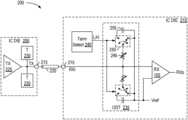
- FIG. 2depicts a communication system 200 in accordance with another embodiment.
- System 200has features in common with IC die 100 of FIG. 1 , like-numbered elements being the same or similar.
- System 200includes ODT circuitry that can selectively introduce filter elements that may be useful for low power configurations. Further, the selection can be accomplished dynamically in some embodiments, which allows system 200 to select appropriate ODT characteristics for high and low-frequency communication. This flexibility is useful for example in systems that support both a low-frequency, power-saving mode and a high-frequency, high-performance mode.
- System 200includes a transmitter IC die 205 coupled to a receiver IC die 210 via a single-ended communication port made up of pads 215 , a channel 220 , and related conductors on dies 205 and 210 .
- Die 205includes a transmitter 225 and a pair of termination legs 230 .
- Legs 230may be the same or similar to the termination legs detailed in connection with the receiver dies 100 and 210 of FIGS. 1 and 2 .
- Transmitter 225conveys a signal TX to receiver 105 on die 210 via pad 215 and the other elements of the associated communication port.
- IC die 210includes ODT circuitry 235 that can select either a filtered or unfiltered half-supply termination topology.
- the termination topologyis then left to the discretion of the user of IC die 210 .
- the topologymay be fixed, defined at start up, or allowed to change dynamically to support different performance modes.
- termination select logic 240issues a control signal L/H, the state of which identifies either a lower-performance, lower-power mode, or a higher-performance, higher-power mode.
- ODT circuitry 235includes two termination legs extending from the communication port between pad 215 and receiver 105 of die 210 .
- the upper termination legincludes a first termination impedance 245 and a first termination switch 250 .
- Switch 250includes three switch nodes, two of which are connected to reference voltage Vref, one directly and the other via a filter capacitor 255 .
- the third switch nodeis coupled to the communication port via termination impedance 245 .
- the lower termination legis substantially the same.
- the switches of the upper and lower termination legsare responsive to signal L/H from termination select logic 240 .
- the switches of both termination legsconnect their respective termination resistors directly to voltage node Vref in a high-performance mode, and to voltage node Vref via a respective filter capacitor in a low-frequency mode. Filtering the input signal in the low-frequency mode advantageously dampens high-frequency noise components.
- the filter capacitorsmay be adjustable in some embodiments to allow filter tuning. Fixed or adjustable resistors in series and/or in parallel with the filter capacitors can also be included.
- FIG. 3depicts an IC die 300 in accordance with another embodiment.
- Die 300includes a receiver 305 that compares an input signal RXi with a reference voltage Vref on a like-named voltage node to produce an output signal RXo.
- Die 300also includes programmable ODT circuitry 310 that can be programmed to provide filtered or unfiltered rail-to-rail or a half-supply termination topologies, and thus combines the functionality of the embodiments of FIGS. 1 and 2 .
- ODT circuitry 310includes two termination legs. Each leg includes switches 315 and 320 , a filter capacitor 325 , and a termination impedance 330 . Switches 315 and 320 support four modes as follows:
- FIG. 4depicts a communication system 400 that employs configurable ODT circuitry in accordance with another embodiment.
- the configurable ODT circuitryallows a transmitter die 405 to select between two or more termination voltages when transmitting data to a receiver die 410 over a differential communication channel 415 .
- the resulting output common-mode voltagecan thus be tailored to the needs of a receiver on die 410 . If, for example, multiple receivers timeshare a common bus but require or benefit from different receive termination voltages, then the associated transmitter or transmitters can use the termination voltage best suited for the receiver with which they are communicating.
- a communication channelmay also support different operational modes that require or benefit from different termination voltages.
- a transmittermight, for example, support a loop-back communication mode for self test or initialization that employs a first termination voltage, and additionally support one or more operational modes that employ different termination voltages suitable for one or more target receivers.
- Die 405includes a differential transmitter with two identical or nearly identical termination legs. Each leg includes a fixed or adjustable termination impedance 417 and a voltage-select switch 420 .
- the state of switches 420are controlled using select signal S that may be provided externally or internally, as by a memory 425 .
- Control logiccan be included to dynamically alter the states of switches 420 , which can alternatively select either of two termination voltages V 1 and V 2 .
- a variable voltage sourceis used in lieu of switches 420 and the two supply nodes.
- FIG. 5depicts a communication system 500 in accordance with yet another embodiment.
- Communication system 500includes a transmitting die 505 communicating with a receiving die 510 via a differential channel 515 .
- the transmitting dieincludes differential output pads 513 coupled via the channel to input pads 517 of the receiving die.
- communication system 500includes a transmitter 520 that employs low-voltage differential signaling (LVDS) for serial data transmission to a corresponding receiver 525 , though other types of signaling may also be used.
- System 500optionally includes an external differential termination resistor 530 (in phantom).
- Die 510includes programmable ODT circuitry that can select from a number of possible termination topologies.
- die 510includes three termination legs that extend from a common node 535 , two to the differential input terminals to receiver 525 and one to a reference voltage node, e.g. ground.
- Each of the first two termination legsincludes a termination impedance 540 and a switch 545 connected in series.
- the third termination legincludes a capacitance 550 , a termination impedance 555 , and a switch 560 .
- the inclusion of impedances 540 and as associated switches 545allows for the omission of external resistor 530 .
- the third legallows for the selective incorporation of a noise-reducing RC filter.
- the impedances and capacitance of the ODT circuitry of FIG. 5are variable in some embodiments, which allows filter and termination values to be trimmed for improved performance.
- Switches 545 and 560can be controlled by external or internal control signals applied to switch control terminals (not shown).
- the various capacitive and resistive elementscan be similarly controlled.
- FIG. 6depicts a configurable RC circuit 600 that can be used in place of the third termination leg of die 510 of FIG. 5 , which extends between node 535 and ground.
- Circuit 600includes some memory 605 , the outputs of which are coupled to the control terminals of a plurality of transistors 610 .
- the transistors 610selectively couple one or more differently sized capacitors 615 between node 535 and ground.
- the resistance between nodes 535 and groundcan be adjusted by selecting various combinations of transistors.
- the width-to-length ratios of transistors 610may be varied to provide various impedances so that enabling different combinations of transistors provides different levels of termination impedance.
- circuit elements or circuit blocksmay be shown or described as multi-conductor or single conductor signal lines.
- Each of the multi-conductor signal linesmay alternatively be single-conductor signal lines, and each of the single-conductor signal lines may alternatively be multi-conductor signal lines.
- Signals and signaling paths shown or described as being single-endedmay also be differential, and vice-versa.
- signals described or depicted as having active-high or active-low logic levelsmay have opposite logic levels in alternative embodiments.
- circuits described or depicted as including metal oxide semiconductor (MOS) transistorsmay alternatively be implemented using bipolar technology or any other technology in which a signal-controlled current flow may be achieved.
- a signalis said to be “asserted” when the signal is driven to a low or high logic state (or charged to a high logic state or discharged to a low logic state) to indicate a particular condition.
- a signalis said to be “de-asserted” to indicate that the signal is driven (or charged or discharged) to a state other than the asserted state (including a high or low logic state, or the floating state that may occur when the signal driving circuit is transitioned to a high impedance condition, such as an open drain or open collector condition).
- a signal driving circuitis said to “output” a signal to a signal receiving circuit when the signal driving circuit asserts (or de-asserts, if explicitly stated or indicated by context) the signal on a signal line coupled between the signal driving and signal receiving circuits.
- An output of a process for designing an integrated circuit, or a portion of an integrated circuit, comprising one or more of the circuits described hereinmay be a computer-readable medium such as, for example, a magnetic tape or an optical or magnetic disk.
- the computer-readable mediummay be encoded with data structures or other information describing circuitry that may be physically instantiated as an integrated circuit or portion of an integrated circuit.
- data structuresare commonly written in Caltech Intermediate Format (CIF), Calma GDS II Stream Format (GDSII), or Electronic Design Interchange Format (EDIF).
- CIFCaltech Intermediate Format
- GDSIICalma GDS II Stream Format
- EDIFElectronic Design Interchange Format
- the embodimentscan be adapted for use with various single-ended and differential communication schemes over unidirectional and bidirectional channels.
- Specific examplesinclude Series Stub Terminated Logic (SSTL) and double-data-rate (DDR) signaling, though this is by no means an exhaustive list.
- SSTLSeries Stub Terminated Logic
- DDRdouble-data-rate
- Embodimentsmay also be used for channels employing various modulation schemes, including those that employ multi-pulse-amplitude-modulation (multi-PAM) and single-PAM signals.
- multi-PAMmulti-pulse-amplitude-modulation
- some componentsare shown directly connected to one another while others are shown connected via intermediate components.
Landscapes
- Engineering & Computer Science (AREA)
- Computer Networks & Wireless Communication (AREA)
- Signal Processing (AREA)
- Power Engineering (AREA)
- Computing Systems (AREA)
- Computer Hardware Design (AREA)
- Physics & Mathematics (AREA)
- General Engineering & Computer Science (AREA)
- Mathematical Physics (AREA)
- Logic Circuits (AREA)
- Dc Digital Transmission (AREA)
- Semiconductor Integrated Circuits (AREA)
- Design And Manufacture Of Integrated Circuits (AREA)
- Networks Using Active Elements (AREA)
Abstract
Description
The subject matter presented herein relates generally to the field of communications, and more particularly to high speed electronic signaling within and between integrated circuit devices.
High-speed data communication integrated circuit (IC) dies are known to include both drivers and receivers. The driver of one such IC connects to the receiver of another via one or more signal transmission lines. Both the driver and receiver circuits include termination elements that attempt to match the characteristic impedance of the transmission line to the output impedance of the driver and input impedance of the receiver, as impedance mismatches degrade signal quality and consequently reduce communication speed and reliability.
Some conventional communication systems employ control systems that calibrate the impedance of on-die termination (ODT) elements for improved impedance matching. These systems work well in many applications. Still, high-speed data communication circuits often must achieve ever-greater performance levels, at competitive prices, to satisfy customer demand. Furthermore, different customers typically have different requirements that may not be met by a given ODT configuration. One customer might favor power-efficiency over speed, or may prefer different termination voltages or impedances. There is therefore a need for ODT circuits that offer customers access to a broader range of termination topologies and values.
The subject matter presented herein is illustrated by way of example, and not by way of limitation, in the figures of the accompanying drawings and in which like reference numerals refer to similar elements and in which:
In rail-to-rail or serial terminations, the communication channel is coupled to each of two opposite supply voltages via a pair of termination impedances. To select a rail-to-rail termination topology,switches receiver 105 is coupled to Vodt and ground viarespective impedances
In half-supply or parallel terminations, the communication channel is coupled to a reference voltage between the two supply voltages. To select a half-supply termination topology,switches receiver 105 is coupled to the reference voltage terminal Vref viaparallel impedances
IC die100 optionally includes acoupling switch 145 betweenpad 110 and the input terminal ofreceiver 105. An external or internal signal, such as frommemory 120, can deliver a signal AC/DC to temporarily or permanently open orclose switch 145. Whenswitch 145 is closed,receiver 105 is DC coupled to pad110: when open,receiver 105 is AC coupled topad 110 via acapacitor 150.
IC die210 includesODT circuitry 235 that can select either a filtered or unfiltered half-supply termination topology. The termination topology is then left to the discretion of the user of IC die210. The topology may be fixed, defined at start up, or allowed to change dynamically to support different performance modes. In the depicted embodiment, terminationselect logic 240 issues a control signal L/H, the state of which identifies either a lower-performance, lower-power mode, or a higher-performance, higher-power mode.
The switches of both termination legs connect their respective termination resistors directly to voltage node Vref in a high-performance mode, and to voltage node Vref via a respective filter capacitor in a low-frequency mode. Filtering the input signal in the low-frequency mode advantageously dampens high-frequency noise components. The filter capacitors may be adjustable in some embodiments to allow filter tuning. Fixed or adjustable resistors in series and/or in parallel with the filter capacitors can also be included.
- 1. Unfiltered Rail-to-Rail: Switches320 are closed and switches315 of the upper and lower termination legs select nodes Vodt and Ground, respectively.
- 2. Filtered Rail-to-Rail: Switches320 are open and switches315 of the upper and lower termination legs select nodes Vodt and Ground, respectively.
- 3. Unfiltered Half-Supply: Switches320 are closed and switches315 both select node Vref.
- 4. Filtered Half-Supply: Switches320 are open and switches315 both select node Vref.
ODT circuitry 310 can be adapted to support more modes. Additional supply voltages can be supported, for example, and the impedances and capacitances can be adjustable.
Die405 includes a differential transmitter with two identical or nearly identical termination legs. Each leg includes a fixed oradjustable termination impedance 417 and a voltage-select switch 420. The state ofswitches 420 are controlled using select signal S that may be provided externally or internally, as by amemory 425. Control logic can be included to dynamically alter the states ofswitches 420, which can alternatively select either of two termination voltages V1 and V2. In other embodiments, a variable voltage source is used in lieu ofswitches 420 and the two supply nodes.
In the foregoing description and in the accompanying drawings, specific terminology and drawing symbols are set forth to provide a thorough understanding of the present invention. In some instances, the terminology and symbols may imply specific details that are not required to practice the invention. For example, the interconnection between circuit elements or circuit blocks may be shown or described as multi-conductor or single conductor signal lines. Each of the multi-conductor signal lines may alternatively be single-conductor signal lines, and each of the single-conductor signal lines may alternatively be multi-conductor signal lines. Signals and signaling paths shown or described as being single-ended may also be differential, and vice-versa. Similarly, signals described or depicted as having active-high or active-low logic levels may have opposite logic levels in alternative embodiments. As another example, circuits described or depicted as including metal oxide semiconductor (MOS) transistors may alternatively be implemented using bipolar technology or any other technology in which a signal-controlled current flow may be achieved. With respect to terminology, a signal is said to be “asserted” when the signal is driven to a low or high logic state (or charged to a high logic state or discharged to a low logic state) to indicate a particular condition. Conversely, a signal is said to be “de-asserted” to indicate that the signal is driven (or charged or discharged) to a state other than the asserted state (including a high or low logic state, or the floating state that may occur when the signal driving circuit is transitioned to a high impedance condition, such as an open drain or open collector condition). A signal driving circuit is said to “output” a signal to a signal receiving circuit when the signal driving circuit asserts (or de-asserts, if explicitly stated or indicated by context) the signal on a signal line coupled between the signal driving and signal receiving circuits.
An output of a process for designing an integrated circuit, or a portion of an integrated circuit, comprising one or more of the circuits described herein may be a computer-readable medium such as, for example, a magnetic tape or an optical or magnetic disk. The computer-readable medium may be encoded with data structures or other information describing circuitry that may be physically instantiated as an integrated circuit or portion of an integrated circuit. Although various formats may be used for such encoding, these data structures are commonly written in Caltech Intermediate Format (CIF), Calma GDS II Stream Format (GDSII), or Electronic Design Interchange Format (EDIF). Those of skill in the art of integrated circuit design can develop such data structures from schematic diagrams of the type detailed above and the corresponding descriptions and encode the data structures on computer readable medium. Those of skill in the art of integrated circuit fabrication can use such encoded data to fabricate integrated circuits comprising one or more of the circuits described herein.
While the present invention has been described in connection with specific embodiments, variations of these embodiments will be obvious to those of ordinary skill in the art. For example, the embodiments can be adapted for use with various single-ended and differential communication schemes over unidirectional and bidirectional channels. Specific examples include Series Stub Terminated Logic (SSTL) and double-data-rate (DDR) signaling, though this is by no means an exhaustive list. Embodiments may also be used for channels employing various modulation schemes, including those that employ multi-pulse-amplitude-modulation (multi-PAM) and single-PAM signals. Moreover, some components are shown directly connected to one another while others are shown connected via intermediate components. In each instance the method of interconnection, or “coupling,” establishes some desired electrical communication between two or more circuit nodes, or terminals. Such coupling may often be accomplished using a number of circuit configurations, as will be understood by those of skill in the art. Therefore, the spirit and scope of the appended claims should not be limited to the foregoing description. Only those claims specifically reciting “means for” or “step for” should be construed in the manner required under the sixth paragraph of 35 U.S.C. § 112.
Claims (20)
1. An integrated-circuit die comprising:
a receiver having an input terminal and an output terminal;
a first switch having a first node coupled to a reference, a second node, and a third node, wherein the first switch selectively couples the first node to the third node and selectively couples the second node to the third node;
a first termination element coupled between the third node and the input terminal;
a second switch having a fourth node coupled to the reference, a fifth node, and a sixth node, wherein the second switch selectively couples the fourth node to the sixth node and selectively couples the fifth node to the sixth node; and
a second termination element coupled between the sixth node and the input terminal.
2. The die ofclaim 1 , wherein the first switch couples the first and third nodes and the second switch couples the fourth and sixth nodes in a serial termination configuration, and wherein the first switch couples the second and third nodes and the second switch couples the fifth and sixth nodes in a parallel termination configuration.
3. The die ofclaim 2 , wherein the first switch and the second switch include respective first and second control terminals.
4. The die ofclaim 3 , further comprising a register with an output port coupled to the first and second control terminals, the register to store a value that determines whether the first and second switches support the parallel termination configuration or the series termination configuration.
5. The die ofclaim 1 , further comprising a first reference-voltage node coupled to the second node and a second reference-voltage node coupled to the fifth node.
6. The die ofclaim 1 , further comprising a third switch and a capacitor coupled in parallel between the pad and the input terminal of the receiver.
7. A communication system comprising:
a first IC die having:
an output pad; and
a transmitter coupled to the output pad to transmit data on the output pad;
a second IC die having:
an input pad; and
a receiver coupled to the input pad to receive the transmit data;
a communication channel extending between the output pad of the first IC die and the input pad of the second IC die; and
a termination circuit integrated with one of the first and second IC dies and coupled to a respective one of the output pad and the input pad, the termination circuit including:
a first switch having a first node coupled to a first reference, a second node, and a third node, wherein the first switch selectively couples the first node to the third node and selectively couples the second node to the third node;
a first termination element coupled between the third node and the input pad;
a second switch having a fourth node coupled to a second reference, a fifth node, and a sixth node, wherein the second switch selectively couples one of the fourth node to the sixth node and selectively couples the fifth nodes node to the sixth node; and
a second termination element coupled between the sixth node and the input pad.
8. The communication system ofclaim 7 , wherein the first switch couples the first and third nodes and the second switch couples the fourth and sixth nodes in a serial termination configuration, and wherein the first switch couples the second and third nodes and the second switch couples the fifth and sixth nodes in a parallel termination configuration.
9. The communication system ofclaim 8 , wherein the first and second switches include respective first and second control terminals.
10. The communication system ofclaim 9 , further comprising a register with an output port coupled to the first and second control terminals, the register to store a value that determines whether the first and second switches support a parallel termination configuration or a series termination configuration.
11. The communication system ofclaim 7 , further comprising a first reference-voltage node coupled to the second node and a second reference-voltage node coupled to the fifth node.
12. The communication system ofclaim 7 , further comprising a capacitor coupled between the first and second nodes.
13. An integrated-circuit die comprising:
a pad to receive an input signal to the die;
a receiver having an input terminal coupled to the pad, a reference, and an output terminal;
a first switch having a first control terminal, a first node coupled to the reference, a second node, and a third node, wherein the first switch selectively couples the first node to the third node and selectively couples the second node to the third node;
a first termination element coupled between the third node and the input terminal;
a second switch having a second control terminal, a fourth node coupled to the reference, a fifth node, and a sixth node, wherein the second switch selectively couples the fourth node to the sixth node and selectively couples the fifth node to the sixth node;
a second termination element coupled between the sixth node and the input terminal; and
a register with an output port coupled to the first control terminal, the register to store a value that determines whether the first switch supports a parallel termination configuration or a series termination configuration.
14. The integrated-circuit die ofclaim 13 , wherein the register output port is coupled to the second control terminal and the value determines whether the second switch supports the parallel termination configuration or the series termination configuration.
15. The integrated-circuit die ofclaim 13 , wherein the first termination element includes a tunable capacitance.
16. The integrated-circuit die ofclaim 15 , wherein the output port of the register is coupled to the first termination element, and wherein the value selects from among a range of capacitances for the tunable capacitance.
17. The integrated-circuit die ofclaim 13 , wherein the register output port is coupled to the first termination element, and wherein the value determines a resistance of the termination element.
18. The integrated-circuit die ofclaim 13 , wherein the input terminal of the receiver is coupled to the pad via a third switch.
19. The integrated-circuit die ofclaim 18 , further comprising a capacitor coupled in parallel with the third switch.
20. The integrated-circuit die ofclaim 18 , wherein the capacitor is tunable over a range of capacitances.
Priority Applications (2)
| Application Number | Priority Date | Filing Date | Title |
|---|---|---|---|
| US18/504,032US12224748B2 (en) | 2005-12-19 | 2023-11-07 | Integrated circuit with configurable on-die termination |
| US19/011,316US20250202487A1 (en) | 2005-12-19 | 2025-01-06 | Integrated circuit with configurable on-die termination |
Applications Claiming Priority (13)
| Application Number | Priority Date | Filing Date | Title |
|---|---|---|---|
| US11/313,054US7439760B2 (en) | 2005-12-19 | 2005-12-19 | Configurable on-die termination |
| US12/288,612US7772876B2 (en) | 2005-12-19 | 2008-10-21 | Configurable on-die termination |
| US12/790,381US7948262B2 (en) | 2005-12-19 | 2010-05-28 | Configurable on-die termination |
| US13/023,993US8072235B2 (en) | 2005-12-19 | 2011-02-09 | Integrated circuit with configurable on-die termination |
| US13/312,762US8466709B2 (en) | 2005-12-19 | 2011-12-06 | Integrated circuit with configurable on-die termination |
| US13/906,219US8941407B2 (en) | 2005-12-19 | 2013-05-30 | Integrated circuit with configurable on-die termination |
| US14/598,990US9338037B2 (en) | 2005-12-19 | 2015-01-16 | Integrated circuit with configurable on-die termination |
| US15/134,513US9685951B2 (en) | 2005-12-19 | 2016-04-21 | Integrated circuit with configurable on-die termination |
| US15/612,455US10236882B2 (en) | 2005-12-19 | 2017-06-02 | Integrated circuit with configurable on-die termination |
| US16/290,749US10651848B2 (en) | 2005-12-19 | 2019-03-01 | Integrated circuit with configurable on-die termination |
| US16/856,645US11012071B2 (en) | 2005-12-19 | 2020-04-23 | Integrated circuit with configurable on-die termination |
| US17/235,283US11843372B2 (en) | 2005-12-19 | 2021-04-20 | Integrated circuit with configurable on-die termination |
| US18/504,032US12224748B2 (en) | 2005-12-19 | 2023-11-07 | Integrated circuit with configurable on-die termination |
Related Parent Applications (1)
| Application Number | Title | Priority Date | Filing Date |
|---|---|---|---|
| US17/235,283ContinuationUS11843372B2 (en) | 2005-12-19 | 2021-04-20 | Integrated circuit with configurable on-die termination |
Related Child Applications (1)
| Application Number | Title | Priority Date | Filing Date |
|---|---|---|---|
| US19/011,316ContinuationUS20250202487A1 (en) | 2005-12-19 | 2025-01-06 | Integrated circuit with configurable on-die termination |
Publications (2)
| Publication Number | Publication Date |
|---|---|
| US20240146304A1 US20240146304A1 (en) | 2024-05-02 |
| US12224748B2true US12224748B2 (en) | 2025-02-11 |
Family
ID=37983601
Family Applications (14)
| Application Number | Title | Priority Date | Filing Date |
|---|---|---|---|
| US11/313,054Active2026-07-24US7439760B2 (en) | 2005-12-19 | 2005-12-19 | Configurable on-die termination |
| US12/288,612ActiveUS7772876B2 (en) | 2005-12-19 | 2008-10-21 | Configurable on-die termination |
| US12/790,381Expired - Fee RelatedUS7948262B2 (en) | 2005-12-19 | 2010-05-28 | Configurable on-die termination |
| US13/023,993ActiveUS8072235B2 (en) | 2005-12-19 | 2011-02-09 | Integrated circuit with configurable on-die termination |
| US13/312,762Expired - Fee RelatedUS8466709B2 (en) | 2005-12-19 | 2011-12-06 | Integrated circuit with configurable on-die termination |
| US13/906,219ActiveUS8941407B2 (en) | 2005-12-19 | 2013-05-30 | Integrated circuit with configurable on-die termination |
| US14/598,990ActiveUS9338037B2 (en) | 2005-12-19 | 2015-01-16 | Integrated circuit with configurable on-die termination |
| US15/134,513ActiveUS9685951B2 (en) | 2005-12-19 | 2016-04-21 | Integrated circuit with configurable on-die termination |
| US15/612,455ActiveUS10236882B2 (en) | 2005-12-19 | 2017-06-02 | Integrated circuit with configurable on-die termination |
| US16/290,749ActiveUS10651848B2 (en) | 2005-12-19 | 2019-03-01 | Integrated circuit with configurable on-die termination |
| US16/856,645ActiveUS11012071B2 (en) | 2005-12-19 | 2020-04-23 | Integrated circuit with configurable on-die termination |
| US17/235,283ActiveUS11843372B2 (en) | 2005-12-19 | 2021-04-20 | Integrated circuit with configurable on-die termination |
| US18/504,032ActiveUS12224748B2 (en) | 2005-12-19 | 2023-11-07 | Integrated circuit with configurable on-die termination |
| US19/011,316PendingUS20250202487A1 (en) | 2005-12-19 | 2025-01-06 | Integrated circuit with configurable on-die termination |
Family Applications Before (12)
| Application Number | Title | Priority Date | Filing Date |
|---|---|---|---|
| US11/313,054Active2026-07-24US7439760B2 (en) | 2005-12-19 | 2005-12-19 | Configurable on-die termination |
| US12/288,612ActiveUS7772876B2 (en) | 2005-12-19 | 2008-10-21 | Configurable on-die termination |
| US12/790,381Expired - Fee RelatedUS7948262B2 (en) | 2005-12-19 | 2010-05-28 | Configurable on-die termination |
| US13/023,993ActiveUS8072235B2 (en) | 2005-12-19 | 2011-02-09 | Integrated circuit with configurable on-die termination |
| US13/312,762Expired - Fee RelatedUS8466709B2 (en) | 2005-12-19 | 2011-12-06 | Integrated circuit with configurable on-die termination |
| US13/906,219ActiveUS8941407B2 (en) | 2005-12-19 | 2013-05-30 | Integrated circuit with configurable on-die termination |
| US14/598,990ActiveUS9338037B2 (en) | 2005-12-19 | 2015-01-16 | Integrated circuit with configurable on-die termination |
| US15/134,513ActiveUS9685951B2 (en) | 2005-12-19 | 2016-04-21 | Integrated circuit with configurable on-die termination |
| US15/612,455ActiveUS10236882B2 (en) | 2005-12-19 | 2017-06-02 | Integrated circuit with configurable on-die termination |
| US16/290,749ActiveUS10651848B2 (en) | 2005-12-19 | 2019-03-01 | Integrated circuit with configurable on-die termination |
| US16/856,645ActiveUS11012071B2 (en) | 2005-12-19 | 2020-04-23 | Integrated circuit with configurable on-die termination |
| US17/235,283ActiveUS11843372B2 (en) | 2005-12-19 | 2021-04-20 | Integrated circuit with configurable on-die termination |
Family Applications After (1)
| Application Number | Title | Priority Date | Filing Date |
|---|---|---|---|
| US19/011,316PendingUS20250202487A1 (en) | 2005-12-19 | 2025-01-06 | Integrated circuit with configurable on-die termination |
Country Status (4)
| Country | Link |
|---|---|
| US (14) | US7439760B2 (en) |
| JP (1) | JP4990910B2 (en) |
| DE (1) | DE112006003478B4 (en) |
| WO (1) | WO2007078496A2 (en) |
Families Citing this family (52)
| Publication number | Priority date | Publication date | Assignee | Title |
|---|---|---|---|---|
| KR100585128B1 (en)* | 2004-02-16 | 2006-05-30 | 삼성전자주식회사 | Semiconductor memory device having different types of termination devices according to frequency of input signals and semiconductor memory system having same |
| US7439760B2 (en) | 2005-12-19 | 2008-10-21 | Rambus Inc. | Configurable on-die termination |
| US7486104B2 (en) | 2006-06-02 | 2009-02-03 | Rambus Inc. | Integrated circuit with graduated on-die termination |
| KR100790821B1 (en)* | 2006-11-15 | 2008-01-03 | 삼성전자주식회사 | On-die termination circuit in semiconductor memory device |
| KR101304456B1 (en)* | 2007-01-19 | 2013-09-04 | 삼성전자주식회사 | Apparatus and method for interfacing data of a printing head chip |
| US10608634B2 (en)* | 2007-06-08 | 2020-03-31 | Conversant Intellectual Property Management Inc. | Dynamic impedance control for input/output buffers |
| US8384423B2 (en)* | 2007-07-19 | 2013-02-26 | Rambus Inc. | Reference voltage and impedance calibration in a multi-mode interface |
| DE102007039616B4 (en)* | 2007-08-22 | 2009-04-09 | Continental Automotive Gmbh | Transceiver circuits |
| US20090080266A1 (en)* | 2007-09-25 | 2009-03-26 | Zumkehr John F | Double data rate (ddr) low power idle mode through reference offset |
| US7649409B1 (en)* | 2007-10-23 | 2010-01-19 | National Semiconductor Corporation | All-pass termination network with equalization and wide common-mode range |
| US7936180B2 (en)* | 2008-02-01 | 2011-05-03 | Mediatek Inc. | Serial link transmitter |
| JP4544326B2 (en)* | 2008-03-26 | 2010-09-15 | セイコーエプソン株式会社 | Integrated circuit device, electro-optical device and electronic apparatus |
| JP2009252322A (en)* | 2008-04-09 | 2009-10-29 | Nec Electronics Corp | Semiconductor memory device |
| US7741867B2 (en)* | 2008-10-30 | 2010-06-22 | Hewlett-Packard Development Company, L.P. | Differential on-line termination |
| US9608630B2 (en)* | 2009-05-06 | 2017-03-28 | Micron Technology, Inc. | Reference voltage circuits and on-die termination circuits, methods for updating the same, and methods for tracking supply, temperature, and/or process variation |
| KR20110003725A (en)* | 2009-07-06 | 2011-01-13 | 삼성전자주식회사 | Transceiver for controlling the swing width of output voltage and its method |
| US8188615B2 (en) | 2009-09-18 | 2012-05-29 | Ati Technologies Ulc | Integrated circuit adapted to be selectively AC or DC coupled |
| US20110133773A1 (en)* | 2009-12-04 | 2011-06-09 | Uniram Technology Inc. | High Performance Output Drivers and Anti-Reflection Circuits |
| US8188764B2 (en)* | 2010-03-18 | 2012-05-29 | Sandisk Technologies Inc. | Efficient electrical hibernate entry and recovery |
| CN102859598A (en) | 2010-06-17 | 2013-01-02 | 拉姆伯斯公司 | Balanced on-die termination |
| GB2486274A (en)* | 2010-12-10 | 2012-06-13 | Microsemi Semiconductor Corp | A programmable bias circuit for the centre node of a balanced receiver termination circuit |
| JP5421300B2 (en)* | 2011-01-19 | 2014-02-19 | 日本電信電話株式会社 | Clock input interface circuit |
| US8487650B2 (en) | 2011-01-25 | 2013-07-16 | Rambus Inc. | Methods and circuits for calibrating multi-modal termination schemes |
| TWI445301B (en)* | 2011-03-03 | 2014-07-11 | Realtek Semiconductor Corp | Transceiving circuit and transceiving circuit resistance calibration method |
| US9224430B2 (en) | 2011-07-27 | 2015-12-29 | Micron Technology, Inc. | Devices, methods, and systems supporting on unit termination |
| WO2013115920A1 (en)* | 2012-01-31 | 2013-08-08 | Rambus Inc. | Modulated on-die termination |
| US9373384B2 (en)* | 2012-04-02 | 2016-06-21 | Rambus Inc. | Integrated circuit device having programmable input capacitance |
| US8611385B2 (en) | 2012-05-17 | 2013-12-17 | Lsi Corporation | Optical source driver circuit with controllable termination |
| TWI493890B (en)* | 2012-07-24 | 2015-07-21 | Novatek Microelectronics Corp | Reception circuit |
| US8836383B2 (en)* | 2012-09-07 | 2014-09-16 | Richtek Technology Corporation | Multipurpose half bridge signal output circuit |
| TWI469510B (en)* | 2012-10-09 | 2015-01-11 | Novatek Microelectronics Corp | Interface circuit |
| US9525571B2 (en) | 2013-03-05 | 2016-12-20 | Lattice Semiconductor Corporation | Calibration of single-ended high-speed interfaces |
| US8912819B2 (en)* | 2013-03-18 | 2014-12-16 | Mediatek Inc. | Termination circuits capable of receiving data signals in different formats for performing impedance matching |
| US8994399B2 (en)* | 2013-04-29 | 2015-03-31 | Broadcom Corporation | Transmission line driver with output swing control |
| US9444455B2 (en) | 2013-12-10 | 2016-09-13 | Sandisk Technologies Llc | Load impedance adjustment for an interface of a data storage device |
| KR20150113587A (en)* | 2014-03-31 | 2015-10-08 | 에스케이하이닉스 주식회사 | Semiconductor device |
| WO2016164019A1 (en)* | 2015-04-09 | 2016-10-13 | Hewlett Packard Enterprise Development Lp | Termination voltage circuits |
| US9910482B2 (en)* | 2015-09-24 | 2018-03-06 | Qualcomm Incorporated | Memory interface with adjustable voltage and termination and methods of use |
| US9871518B2 (en)* | 2016-02-02 | 2018-01-16 | Mediatek Inc. | Memory interface circuit capable of controlling driving ability and associated control method |
| US20170243628A1 (en)* | 2016-02-22 | 2017-08-24 | Mediatek Inc. | Termination topology of memory system and associated memory module and control method |
| CN105931593B (en)* | 2016-06-30 | 2019-03-19 | 深圳市华星光电技术有限公司 | The display device of circuit structure with the more receiving ends VBO |
| US11450613B2 (en)* | 2018-03-23 | 2022-09-20 | Intel Corporation | Integrated circuit package with test circuitry for testing a channel between dies |
| US10484044B1 (en)* | 2018-05-01 | 2019-11-19 | Huawei Technologies Co., Ltd. | Differential termination modulation for back-channel communication |
| US10411703B1 (en)* | 2018-06-05 | 2019-09-10 | Samsung Electronics Co., Ltd. | Impedance matched clock driver with amplitude control |
| US10592458B1 (en)* | 2018-09-18 | 2020-03-17 | Apple Inc. | Bimodal impedance matching terminators |
| KR20200115805A (en) | 2019-03-26 | 2020-10-08 | 삼성전자주식회사 | Receiver for compensating common mode offset |
| US11409354B2 (en)* | 2019-04-22 | 2022-08-09 | Micron Technology, Inc. | Multi-voltage operation for driving a multi-mode channel |
| KR102787325B1 (en) | 2020-09-11 | 2025-03-27 | 삼성전자주식회사 | Transmitter for generating multi-level signal and memory system including the same |
| US11196247B1 (en)* | 2020-10-19 | 2021-12-07 | Dyna Image Corporation | Digital device using three states |
| CN116941225A (en)* | 2021-03-01 | 2023-10-24 | 罗姆股份有限公司 | Sending circuits, electronic control units and vehicles |
| JP2025019640A (en)* | 2023-07-28 | 2025-02-07 | ローム株式会社 | Receiver circuit, semiconductor device, and communication system |
| KR102823144B1 (en)* | 2023-11-08 | 2025-06-20 | 광운대학교 산학협력단 | VM Termination based driver Apparatus for PAM-3 modulater signer |
Citations (119)
| Publication number | Priority date | Publication date | Assignee | Title |
|---|---|---|---|---|
| US4584695A (en) | 1983-11-09 | 1986-04-22 | National Semiconductor Corporation | Digital PLL decoder |
| US4590396A (en) | 1982-07-26 | 1986-05-20 | Tokyo Shibaura Denki Kabushiki Kaisha | Integrated MOSFET transfer gate |
| JPH02140676A (en) | 1988-11-21 | 1990-05-30 | Advantest Corp | Multilevel driving circuit |
| EP0520687A1 (en) | 1991-06-28 | 1992-12-30 | AT&T Corp. | Digitally controlled element sizing |
| US5254883A (en) | 1992-04-22 | 1993-10-19 | Rambus, Inc. | Electrical current source circuitry for a bus |
| US5298800A (en) | 1991-06-28 | 1994-03-29 | At&T Bell Laboratories | Digitally controlled element sizing |
| US5396028A (en) | 1993-05-05 | 1995-03-07 | Texas Instruments Incorporated | Method and apparatus for transmission line termination |
| US5406147A (en) | 1993-06-18 | 1995-04-11 | Digital Equipment Corporation | Propagation speedup by use of complementary resolver outputs in a system bus receiver |
| US5467455A (en) | 1993-11-03 | 1995-11-14 | Motorola, Inc. | Data processing system and method for performing dynamic bus termination |
| US5523703A (en) | 1993-09-17 | 1996-06-04 | Fujitsu Limited | Method and apparatus for controlling termination of current driven circuits |
| US5528168A (en) | 1995-03-29 | 1996-06-18 | Intel Corporation | Power saving terminated bus |
| US5544067A (en) | 1990-04-06 | 1996-08-06 | Lsi Logic Corporation | Method and system for creating, deriving and validating structural description of electronic system from higher level, behavior-oriented description, including interactive schematic design and simulation |
| WO1997002658A1 (en) | 1995-07-03 | 1997-01-23 | Intel Corporation | Mos termination for low power signaling |
| US5663661A (en) | 1995-04-04 | 1997-09-02 | Rambus, Inc. | Modular bus with single or double parallel termination |
| US5666078A (en) | 1996-02-07 | 1997-09-09 | International Business Machines Corporation | Programmable impedance output driver |
| US5680060A (en) | 1994-12-22 | 1997-10-21 | Alcatel Nv | Method of and circuit arrangement for terminating a line connected to a CMOS integrated circuit |
| EP0817441A2 (en) | 1996-06-26 | 1998-01-07 | Lucent Technologies Inc. | Integrated circuit chip with adaptive input-output port |
| WO1998004041A1 (en) | 1996-07-19 | 1998-01-29 | Kaplinsky Cecil H | Programmable dynamic line-termination circuit |
| US5726582A (en) | 1994-02-25 | 1998-03-10 | Telefonaktiebolget Lm Ericsson | Control circuit for keeping constant the impedance of a termination network |
| US5781028A (en) | 1996-06-21 | 1998-07-14 | Microsoft Corporation | System and method for a switched data bus termination |
| US5926031A (en) | 1996-10-29 | 1999-07-20 | Linfinitymicroelectronics, Inc. | High speed digital bus termination |
| US5939986A (en) | 1996-10-18 | 1999-08-17 | The United States Of America As Represented By The United States Department Of Energy | Mobile machine hazardous working zone warning system |
| US5969658A (en) | 1997-11-18 | 1999-10-19 | Burr-Brown Corporation | R/2R ladder circuit and method for digital-to-analog converter |
| US5982191A (en) | 1997-06-25 | 1999-11-09 | Sun Microsystems, Inc. | Broadly distributed termination for buses using switched terminator logic |
| US5995894A (en) | 1997-05-27 | 1999-11-30 | Case Corporation | System for analyzing spatially-variable harvest data by pass |
| US6028484A (en) | 1998-02-10 | 2000-02-22 | Acuson Corporation | Ultrasound apparatus and method for amplifying transmit signals |
| US6040714A (en) | 1997-12-12 | 2000-03-21 | Micron Electronics, Inc. | Method for providing two modes of I/O pad termination |
| US6060907A (en) | 1997-06-25 | 2000-05-09 | Sun Microsystems, Inc. | Impedance control circuit |
| US6064224A (en) | 1998-07-31 | 2000-05-16 | Hewlett--Packard Company | Calibration sharing for CMOS output driver |
| US6072943A (en) | 1997-12-30 | 2000-06-06 | Lsi Logic Corporation | Integrated bus controller and terminating chip |
| WO2000041300A1 (en) | 1998-12-31 | 2000-07-13 | Intel Corporation | On-chip termination |
| WO2000070474A1 (en) | 1999-05-19 | 2000-11-23 | Sun Microsystems, Inc. | Apparatus for reducing reflections when using dynamic termination logic signaling |
| US6232792B1 (en) | 1997-06-25 | 2001-05-15 | Sun Microsystems, Inc. | Terminating transmission lines using on-chip terminator circuitry |
| US6266001B1 (en) | 1999-05-05 | 2001-07-24 | Maxim Integrated Products, Inc. | Method and apparatus for switching low voltage CMOS switches in high voltage digital to analog converters |
| US6288564B1 (en) | 1997-08-19 | 2001-09-11 | Telefonaktiebolaget Lm Ercisson | Line receiver circuit with line termination impedance |
| US6308232B1 (en) | 1999-09-01 | 2001-10-23 | Rambus Inc. | Electronically moveable terminator and method for using same in a memory system |
| US20010047450A1 (en) | 1998-07-27 | 2001-11-29 | Peter Gillingham | High bandwidth memory interface |
| US6344765B2 (en) | 1996-08-29 | 2002-02-05 | Fujitsu Limited | Signal transmission with reduced ringing of signals |
| US6353334B1 (en) | 2000-01-27 | 2002-03-05 | Xilinx, Inc. | Circuit for converting a logic signal on an output node to a pair of low-voltage differential signals |
| US6356105B1 (en) | 2000-06-28 | 2002-03-12 | Intel Corporation | Impedance control system for a center tapped termination bus |
| US6356106B1 (en) | 2000-09-12 | 2002-03-12 | Micron Technology, Inc. | Active termination in a multidrop memory system |
| US6366128B1 (en) | 2000-09-05 | 2002-04-02 | Xilinx, Inc. | Circuit for producing low-voltage differential signals |
| US6411122B1 (en) | 2000-10-27 | 2002-06-25 | Intel Corporation | Apparatus and method for dynamic on-die termination in an open-drain bus architecture system |
| US6418500B1 (en) | 1999-02-12 | 2002-07-09 | Fujitsu Limited | Feedback control for termination adjustment |
| US6424170B1 (en) | 2001-05-18 | 2002-07-23 | Intel Corporation | Apparatus and method for linear on-die termination in an open drain bus architecture system |
| WO2002063833A2 (en) | 2001-02-06 | 2002-08-15 | 2Wire, Inc. | Loop extender with selectable line termination and equalization |
| US6448813B2 (en) | 1998-10-26 | 2002-09-10 | Rambus Inc. | Output driver circuit with well-controlled output impedance |
| US20020130680A1 (en) | 2001-03-15 | 2002-09-19 | Meyer Bruce Alan | Method and apparatus for terminating emitter coupled logic (ECL) transceivers |
| US6462591B2 (en) | 1997-08-29 | 2002-10-08 | Rambus Inc. | Semiconductor memory device having a controlled output driver characteristic |
| US6462588B2 (en) | 2000-04-03 | 2002-10-08 | Rambus, Inc. | Asymmetry control for an output driver |
| US6495997B2 (en) | 2001-02-15 | 2002-12-17 | Intel Corporation | High impedance current mode voltage scalable driver |
| US6509756B1 (en) | 2000-03-31 | 2003-01-21 | Rambus Inc. | Method and apparatus for low capacitance, high output impedance driver |
| US6525558B2 (en) | 2000-11-27 | 2003-02-25 | Samsung Electronics Co., Ltd. | Programmable impedance control circuit |
| US6530062B1 (en) | 2000-03-10 | 2003-03-04 | Rambus Inc. | Active impedance compensation |
| US6535047B2 (en) | 2001-05-17 | 2003-03-18 | Intel Corporation | Apparatus and method to use a single reference component in a master-slave configuration for multiple circuit compensation |
| US6545522B2 (en) | 2001-05-17 | 2003-04-08 | Intel Corporation | Apparatus and method to provide a single reference component for multiple circuit compensation using digital impedance code shifting |
| US6552565B2 (en) | 2001-03-13 | 2003-04-22 | Realtek Semiconductor Corp. | Impedance matching circuit |
| US6573747B2 (en) | 2001-09-28 | 2003-06-03 | Intel Corporation | Digital update scheme for adaptive impedance control of on-die input/output circuits |
| US6573746B2 (en) | 2000-11-30 | 2003-06-03 | Samsung Electronics Co., Ltd. | Impedance control circuit |
| US20030112751A1 (en) | 2001-12-17 | 2003-06-19 | Marcelo Yuffe | Method and apparatus for driving a signal using switchable on-die termination |
| US20030146772A1 (en) | 2002-02-01 | 2003-08-07 | Chaiyuth Chansungsan | Termination pair for a differential driver-differential receiver input output circuit |
| US20040000924A1 (en) | 2002-02-19 | 2004-01-01 | Rambus, Inc. | Method and apparatus for selectably providing single-ended and differential signaling with controllable impedance and transition time |
| US6711073B2 (en) | 2001-11-28 | 2004-03-23 | Micron Technology, Inc. | Active termination circuit and method for controlling the impedance of external integrated circuit terminals |
| US6734702B1 (en) | 2002-11-12 | 2004-05-11 | Texas Instruments Incorporated | Impedance calibration circuit |
| US20040124850A1 (en) | 2002-12-31 | 2004-07-01 | Koneru Surya N. | Calibration circuit for current source and on-die terminations |
| US6762620B2 (en) | 2002-05-24 | 2004-07-13 | Samsung Electronics Co., Ltd. | Circuit and method for controlling on-die signal termination |
| WO2004061690A2 (en) | 2002-12-31 | 2004-07-22 | Intel Corporation | Apparatus and method for bus signal termination compensation during detected quiet cycle |
| US6768352B1 (en) | 2002-11-13 | 2004-07-27 | Cypress Semiconductor Corp. | Low voltage receiver circuit and method for shifting the differential input signals of the receiver depending on a common mode voltage of the input signals |
| US6781405B2 (en) | 2002-04-29 | 2004-08-24 | Rambus Inc. | Adaptive signal termination |
| US20040189343A1 (en) | 2003-03-25 | 2004-09-30 | Seong-Jin Jang | Semiconductor devices with reference voltage generators and termination circuits configured to reduce termination mismatch |
| US6806728B2 (en) | 2001-08-15 | 2004-10-19 | Rambus, Inc. | Circuit and method for interfacing to a bus channel |
| US20040222834A1 (en) | 2003-05-09 | 2004-11-11 | Rambus Inc. | Method and apparatus for signal reception using ground termination and/or non-ground termination |
| US20040246026A1 (en) | 2003-06-06 | 2004-12-09 | Microsoft Corporation | Method and apparatus for multi-mode driver |
| US20050057275A1 (en) | 2003-09-12 | 2005-03-17 | Ngyuen Huy M. | Adaptive impedance output driver circuit |
| US6888370B1 (en) | 2003-08-20 | 2005-05-03 | Altera Corporation | Dynamically adjustable termination impedance control techniques |
| US6894691B2 (en) | 2002-05-01 | 2005-05-17 | Dell Products L.P. | Dynamic switching of parallel termination for power management with DDR memory |
| US6924660B2 (en) | 2003-09-08 | 2005-08-02 | Rambus Inc. | Calibration methods and circuits for optimized on-die termination |
| US6940303B2 (en) | 2002-11-29 | 2005-09-06 | Roy L. Vargas | System and method to establish an adjustable on-chip impedance |
| US20050225353A1 (en) | 2004-04-08 | 2005-10-13 | Hynix Semiconductor Inc. | On die termination circuit |
| US6965529B2 (en) | 2002-06-21 | 2005-11-15 | Intel Coproration | Memory bus termination |
| US6968413B2 (en) | 2002-10-07 | 2005-11-22 | International Business Machines Corporation | Method and system for configuring terminators in a serial communication system |
| WO2005119471A2 (en) | 2004-06-01 | 2005-12-15 | Hewlett-Packard Development Company, L.P. | Bus controller |
| US20050275425A1 (en) | 2004-06-14 | 2005-12-15 | Samsung Electronics Co., Ltd. | Memory system with a scheme capable of stably terminating a pair of differential signals transmitted via a pair of transmission lines |
| US6981089B2 (en) | 2001-12-31 | 2005-12-27 | Intel Corporation | Memory bus termination with memory unit having termination control |
| US6980020B2 (en) | 2003-12-19 | 2005-12-27 | Rambus Inc. | Calibration methods and circuits for optimized on-die termination |
| US20060007761A1 (en) | 2001-04-24 | 2006-01-12 | Ware Frederick A | Memory module with termination component |
| US20060077731A1 (en) | 2001-04-24 | 2006-04-13 | Ware Frederick A | Memory module with termination component |
| US7038498B2 (en) | 2001-10-29 | 2006-05-02 | Elpida Memory, Inc. | Input/output circuit, reference-voltage generating circuit, and semiconductor integrated circuit |
| US7042254B2 (en) | 2003-05-27 | 2006-05-09 | Nec Electronics Corporation | Differential signal receiving device and differential signal transmission system |
| US7068064B1 (en) | 2003-05-12 | 2006-06-27 | Pericom Semiconductor Corp. | Memory module with dynamic termination using bus switches timed by memory clock and chip select |
| US7102200B2 (en) | 2001-09-04 | 2006-09-05 | Intel Corporation | On-die termination resistor with analog compensation |
| US7109744B1 (en) | 2001-12-11 | 2006-09-19 | Altera Corporation | Programmable termination with DC voltage level control |
| US7120390B2 (en) | 2001-03-21 | 2006-10-10 | Agere Systems Inc. | BLUETOOTH smart offset compensation |
| US7123047B2 (en) | 2004-08-18 | 2006-10-17 | Intel Corporation | Dynamic on-die termination management |
| US7135884B1 (en) | 2005-01-13 | 2006-11-14 | Advanced Micro Devices, Inc. | Voltage mode transceiver having programmable voltage swing and external reference-based calibration |
| US7148721B2 (en) | 2003-08-19 | 2006-12-12 | Samsung Electronics Co., Ltd. | Semiconductor integrated circuit device capable of controlling impedance |
| US7161378B2 (en) | 2004-10-30 | 2007-01-09 | Hynix Semiconductor, Inc. | Semiconductor memory device with on die termination circuit |
| US20070007992A1 (en) | 2005-06-30 | 2007-01-11 | Bains Kuljit S | Method to calibrate DRAM Ron and ODT values over PVT |
| US7196567B2 (en) | 2004-12-20 | 2007-03-27 | Rambus Inc. | Systems and methods for controlling termination resistance values for a plurality of communication channels |
| US20070070717A1 (en) | 2005-09-27 | 2007-03-29 | Hynix Semiconductor Inc. | Semiconductor memory device for adjusting impedance of data output driver |
| US7245154B1 (en) | 2005-03-03 | 2007-07-17 | Lattice Semiconductor Corporation | Differential input receiver with programmable failsafe |
| US7245146B2 (en) | 2004-08-31 | 2007-07-17 | Nec Electronics Corporation | Semiconductor device with termination resistance adjusting circuit |
| US7268712B1 (en) | 2006-04-18 | 2007-09-11 | Taiwan Semiconductor Manufacturing Co., Ltd. | System and method for calibrating on-die components |
| US7301371B2 (en) | 2004-09-07 | 2007-11-27 | Samsung Electronics Co., Ltd. | Transmitter of a semiconductor device |
| US7342411B2 (en) | 2005-12-07 | 2008-03-11 | Intel Corporation | Dynamic on-die termination launch latency reduction |
| US20100066404A1 (en) | 2008-09-15 | 2010-03-18 | Zhang yu min | Reduced Power Differential Type Termination Circuit |
| US7772876B2 (en)* | 2005-12-19 | 2010-08-10 | Rambus Inc. | Configurable on-die termination |
| US7843212B2 (en) | 2007-03-12 | 2010-11-30 | Sumitomo Electric Industries, Ltd. | Differential circuit with precisely controlled terminator circuit |
| US20110019760A1 (en) | 2009-07-21 | 2011-01-27 | Rambus Inc. | Methods and Systems for Reducing Supply and Termination Noise |
| US7965104B2 (en) | 2007-06-22 | 2011-06-21 | Nec Corporation | Data transmission system and method, and electronic apparatus provided with same data transmission system |
| US20110267101A1 (en) | 2006-06-02 | 2011-11-03 | Kyung Suk Oh | Controlling dynamic selection of on-die termination |
| US20120187978A1 (en) | 2011-01-25 | 2012-07-26 | Rambus Inc. | Methods and Circuits for Calibrating Multi-Modal Termination Schemes |
| US8798204B2 (en) | 2011-09-09 | 2014-08-05 | International Business Machines Corporation | Serial link receiver for handling high speed transmissions |
| US9281816B2 (en) | 2012-01-31 | 2016-03-08 | Rambus Inc. | Modulated on-die termination |
| US20180004281A1 (en) | 2016-07-01 | 2018-01-04 | Samsung Electronics Co., Ltd. | Reception interface circuit and memory system including the same |
| US9871516B2 (en) | 2014-06-04 | 2018-01-16 | Lattice Semiconductor Corporation | Transmitting apparatus with source termination |
| US9935606B1 (en) | 2016-09-30 | 2018-04-03 | Ali Corporation | System on chip and correction method of termination impedance element thereof |
| US10291275B2 (en) | 2016-03-31 | 2019-05-14 | Samsung Electronics Co., Ltd. | Reception interface circuits supporting multiple communication standards and memory systems including the same |
| US11184196B1 (en) | 2020-12-17 | 2021-11-23 | Omnivision Technologies, Inc. | Impedance matching system for high speed digital receivers |
Family Cites Families (4)
| Publication number | Priority date | Publication date | Assignee | Title |
|---|---|---|---|---|
| US7135584B2 (en)* | 1995-08-07 | 2006-11-14 | Wake Forest University | Lipid analogs for treating viral infections |
| US6147520A (en)* | 1997-12-18 | 2000-11-14 | Lucent Technologies, Inc. | Integrated circuit having controlled impedance |
| KR100860523B1 (en)* | 2002-10-11 | 2008-09-26 | 엘지디스플레이 주식회사 | Transverse electric field liquid crystal display device and manufacturing method thereof |
| US6700823B1 (en)* | 2002-10-30 | 2004-03-02 | Lattice Semiconductor Corporation | Programmable common mode termination for input/output circuits |
- 2005
- 2005-12-19USUS11/313,054patent/US7439760B2/enactiveActive
- 2006
- 2006-11-30DEDE112006003478Tpatent/DE112006003478B4/ennot_activeExpired - Fee Related
- 2006-11-30WOPCT/US2006/045966patent/WO2007078496A2/enactiveApplication Filing
- 2006-11-30JPJP2008547256Apatent/JP4990910B2/enactiveActive
- 2008
- 2008-10-21USUS12/288,612patent/US7772876B2/enactiveActive
- 2010
- 2010-05-28USUS12/790,381patent/US7948262B2/ennot_activeExpired - Fee Related
- 2011
- 2011-02-09USUS13/023,993patent/US8072235B2/enactiveActive
- 2011-12-06USUS13/312,762patent/US8466709B2/ennot_activeExpired - Fee Related
- 2013
- 2013-05-30USUS13/906,219patent/US8941407B2/enactiveActive
- 2015
- 2015-01-16USUS14/598,990patent/US9338037B2/enactiveActive
- 2016
- 2016-04-21USUS15/134,513patent/US9685951B2/enactiveActive
- 2017
- 2017-06-02USUS15/612,455patent/US10236882B2/enactiveActive
- 2019
- 2019-03-01USUS16/290,749patent/US10651848B2/enactiveActive
- 2020
- 2020-04-23USUS16/856,645patent/US11012071B2/enactiveActive
- 2021
- 2021-04-20USUS17/235,283patent/US11843372B2/enactiveActive
- 2023
- 2023-11-07USUS18/504,032patent/US12224748B2/enactiveActive
- 2025
- 2025-01-06USUS19/011,316patent/US20250202487A1/enactivePending
Patent Citations (133)
| Publication number | Priority date | Publication date | Assignee | Title |
|---|---|---|---|---|
| US4590396A (en) | 1982-07-26 | 1986-05-20 | Tokyo Shibaura Denki Kabushiki Kaisha | Integrated MOSFET transfer gate |
| US4584695A (en) | 1983-11-09 | 1986-04-22 | National Semiconductor Corporation | Digital PLL decoder |
| JPH02140676A (en) | 1988-11-21 | 1990-05-30 | Advantest Corp | Multilevel driving circuit |
| US5544067A (en) | 1990-04-06 | 1996-08-06 | Lsi Logic Corporation | Method and system for creating, deriving and validating structural description of electronic system from higher level, behavior-oriented description, including interactive schematic design and simulation |
| EP0520687A1 (en) | 1991-06-28 | 1992-12-30 | AT&T Corp. | Digitally controlled element sizing |
| US5298800A (en) | 1991-06-28 | 1994-03-29 | At&T Bell Laboratories | Digitally controlled element sizing |
| US5254883A (en) | 1992-04-22 | 1993-10-19 | Rambus, Inc. | Electrical current source circuitry for a bus |
| US5396028A (en) | 1993-05-05 | 1995-03-07 | Texas Instruments Incorporated | Method and apparatus for transmission line termination |
| US5406147A (en) | 1993-06-18 | 1995-04-11 | Digital Equipment Corporation | Propagation speedup by use of complementary resolver outputs in a system bus receiver |
| US5523703A (en) | 1993-09-17 | 1996-06-04 | Fujitsu Limited | Method and apparatus for controlling termination of current driven circuits |
| US5467455A (en) | 1993-11-03 | 1995-11-14 | Motorola, Inc. | Data processing system and method for performing dynamic bus termination |
| US5726582A (en) | 1994-02-25 | 1998-03-10 | Telefonaktiebolget Lm Ericsson | Control circuit for keeping constant the impedance of a termination network |
| US5680060A (en) | 1994-12-22 | 1997-10-21 | Alcatel Nv | Method of and circuit arrangement for terminating a line connected to a CMOS integrated circuit |
| US5528168A (en) | 1995-03-29 | 1996-06-18 | Intel Corporation | Power saving terminated bus |
| US5663661A (en) | 1995-04-04 | 1997-09-02 | Rambus, Inc. | Modular bus with single or double parallel termination |
| WO1997002658A1 (en) | 1995-07-03 | 1997-01-23 | Intel Corporation | Mos termination for low power signaling |
| US5666078A (en) | 1996-02-07 | 1997-09-09 | International Business Machines Corporation | Programmable impedance output driver |
| US5781028A (en) | 1996-06-21 | 1998-07-14 | Microsoft Corporation | System and method for a switched data bus termination |
| EP0817441A2 (en) | 1996-06-26 | 1998-01-07 | Lucent Technologies Inc. | Integrated circuit chip with adaptive input-output port |
| WO1998004041A1 (en) | 1996-07-19 | 1998-01-29 | Kaplinsky Cecil H | Programmable dynamic line-termination circuit |
| US6344765B2 (en) | 1996-08-29 | 2002-02-05 | Fujitsu Limited | Signal transmission with reduced ringing of signals |
| US5939986A (en) | 1996-10-18 | 1999-08-17 | The United States Of America As Represented By The United States Department Of Energy | Mobile machine hazardous working zone warning system |
| US5926031A (en) | 1996-10-29 | 1999-07-20 | Linfinitymicroelectronics, Inc. | High speed digital bus termination |
| US5995894A (en) | 1997-05-27 | 1999-11-30 | Case Corporation | System for analyzing spatially-variable harvest data by pass |
| US5982191A (en) | 1997-06-25 | 1999-11-09 | Sun Microsystems, Inc. | Broadly distributed termination for buses using switched terminator logic |
| US6232792B1 (en) | 1997-06-25 | 2001-05-15 | Sun Microsystems, Inc. | Terminating transmission lines using on-chip terminator circuitry |
| US6060907A (en) | 1997-06-25 | 2000-05-09 | Sun Microsystems, Inc. | Impedance control circuit |
| US6288564B1 (en) | 1997-08-19 | 2001-09-11 | Telefonaktiebolaget Lm Ercisson | Line receiver circuit with line termination impedance |
| US6608507B2 (en) | 1997-08-29 | 2003-08-19 | Rambus Inc. | Memory system including a memory device having a controlled output driver characteristic |
| US6462591B2 (en) | 1997-08-29 | 2002-10-08 | Rambus Inc. | Semiconductor memory device having a controlled output driver characteristic |
| US5969658A (en) | 1997-11-18 | 1999-10-19 | Burr-Brown Corporation | R/2R ladder circuit and method for digital-to-analog converter |
| US6040714A (en) | 1997-12-12 | 2000-03-21 | Micron Electronics, Inc. | Method for providing two modes of I/O pad termination |
| US6072943A (en) | 1997-12-30 | 2000-06-06 | Lsi Logic Corporation | Integrated bus controller and terminating chip |
| US6028484A (en) | 1998-02-10 | 2000-02-22 | Acuson Corporation | Ultrasound apparatus and method for amplifying transmit signals |
| US20010047450A1 (en) | 1998-07-27 | 2001-11-29 | Peter Gillingham | High bandwidth memory interface |
| US6064224A (en) | 1998-07-31 | 2000-05-16 | Hewlett--Packard Company | Calibration sharing for CMOS output driver |
| US6448813B2 (en) | 1998-10-26 | 2002-09-10 | Rambus Inc. | Output driver circuit with well-controlled output impedance |
| US6157206A (en) | 1998-12-31 | 2000-12-05 | Intel Corporation | On-chip termination |
| WO2000041300A1 (en) | 1998-12-31 | 2000-07-13 | Intel Corporation | On-chip termination |
| US6418500B1 (en) | 1999-02-12 | 2002-07-09 | Fujitsu Limited | Feedback control for termination adjustment |
| US6266001B1 (en) | 1999-05-05 | 2001-07-24 | Maxim Integrated Products, Inc. | Method and apparatus for switching low voltage CMOS switches in high voltage digital to analog converters |
| WO2000070474A1 (en) | 1999-05-19 | 2000-11-23 | Sun Microsystems, Inc. | Apparatus for reducing reflections when using dynamic termination logic signaling |
| US6308232B1 (en) | 1999-09-01 | 2001-10-23 | Rambus Inc. | Electronically moveable terminator and method for using same in a memory system |
| US6353334B1 (en) | 2000-01-27 | 2002-03-05 | Xilinx, Inc. | Circuit for converting a logic signal on an output node to a pair of low-voltage differential signals |
| US6530062B1 (en) | 2000-03-10 | 2003-03-04 | Rambus Inc. | Active impedance compensation |
| US6509756B1 (en) | 2000-03-31 | 2003-01-21 | Rambus Inc. | Method and apparatus for low capacitance, high output impedance driver |
| US6462588B2 (en) | 2000-04-03 | 2002-10-08 | Rambus, Inc. | Asymmetry control for an output driver |
| US6356105B1 (en) | 2000-06-28 | 2002-03-12 | Intel Corporation | Impedance control system for a center tapped termination bus |
| US6366128B1 (en) | 2000-09-05 | 2002-04-02 | Xilinx, Inc. | Circuit for producing low-voltage differential signals |
| US6356106B1 (en) | 2000-09-12 | 2002-03-12 | Micron Technology, Inc. | Active termination in a multidrop memory system |
| US6411122B1 (en) | 2000-10-27 | 2002-06-25 | Intel Corporation | Apparatus and method for dynamic on-die termination in an open-drain bus architecture system |
| US6661250B2 (en) | 2000-11-27 | 2003-12-09 | Samsung Electronics Co., Ltd. | Programmable impedance control circuit |
| US6525558B2 (en) | 2000-11-27 | 2003-02-25 | Samsung Electronics Co., Ltd. | Programmable impedance control circuit |
| US6573746B2 (en) | 2000-11-30 | 2003-06-03 | Samsung Electronics Co., Ltd. | Impedance control circuit |
| WO2002063833A2 (en) | 2001-02-06 | 2002-08-15 | 2Wire, Inc. | Loop extender with selectable line termination and equalization |
| US6495997B2 (en) | 2001-02-15 | 2002-12-17 | Intel Corporation | High impedance current mode voltage scalable driver |
| US6552565B2 (en) | 2001-03-13 | 2003-04-22 | Realtek Semiconductor Corp. | Impedance matching circuit |
| US20020130680A1 (en) | 2001-03-15 | 2002-09-19 | Meyer Bruce Alan | Method and apparatus for terminating emitter coupled logic (ECL) transceivers |
| US7120390B2 (en) | 2001-03-21 | 2006-10-10 | Agere Systems Inc. | BLUETOOTH smart offset compensation |
| US20060077731A1 (en) | 2001-04-24 | 2006-04-13 | Ware Frederick A | Memory module with termination component |
| US20060007761A1 (en) | 2001-04-24 | 2006-01-12 | Ware Frederick A | Memory module with termination component |
| US6545522B2 (en) | 2001-05-17 | 2003-04-08 | Intel Corporation | Apparatus and method to provide a single reference component for multiple circuit compensation using digital impedance code shifting |
| US6535047B2 (en) | 2001-05-17 | 2003-03-18 | Intel Corporation | Apparatus and method to use a single reference component in a master-slave configuration for multiple circuit compensation |
| US6424170B1 (en) | 2001-05-18 | 2002-07-23 | Intel Corporation | Apparatus and method for linear on-die termination in an open drain bus architecture system |
| US6806728B2 (en) | 2001-08-15 | 2004-10-19 | Rambus, Inc. | Circuit and method for interfacing to a bus channel |
| US7102200B2 (en) | 2001-09-04 | 2006-09-05 | Intel Corporation | On-die termination resistor with analog compensation |
| US6573747B2 (en) | 2001-09-28 | 2003-06-03 | Intel Corporation | Digital update scheme for adaptive impedance control of on-die input/output circuits |
| US7038498B2 (en) | 2001-10-29 | 2006-05-02 | Elpida Memory, Inc. | Input/output circuit, reference-voltage generating circuit, and semiconductor integrated circuit |
| US6711073B2 (en) | 2001-11-28 | 2004-03-23 | Micron Technology, Inc. | Active termination circuit and method for controlling the impedance of external integrated circuit terminals |
| US7109744B1 (en) | 2001-12-11 | 2006-09-19 | Altera Corporation | Programmable termination with DC voltage level control |
| US20030112751A1 (en) | 2001-12-17 | 2003-06-19 | Marcelo Yuffe | Method and apparatus for driving a signal using switchable on-die termination |
| US6981089B2 (en) | 2001-12-31 | 2005-12-27 | Intel Corporation | Memory bus termination with memory unit having termination control |
| US20030146772A1 (en) | 2002-02-01 | 2003-08-07 | Chaiyuth Chansungsan | Termination pair for a differential driver-differential receiver input output circuit |
| US20040000924A1 (en) | 2002-02-19 | 2004-01-01 | Rambus, Inc. | Method and apparatus for selectably providing single-ended and differential signaling with controllable impedance and transition time |
| US6781405B2 (en) | 2002-04-29 | 2004-08-24 | Rambus Inc. | Adaptive signal termination |
| US20040201402A1 (en) | 2002-04-29 | 2004-10-14 | Rambus Inc. | Adaptive signal termination |
| US6894691B2 (en) | 2002-05-01 | 2005-05-17 | Dell Products L.P. | Dynamic switching of parallel termination for power management with DDR memory |
| US6762620B2 (en) | 2002-05-24 | 2004-07-13 | Samsung Electronics Co., Ltd. | Circuit and method for controlling on-die signal termination |
| US6965529B2 (en) | 2002-06-21 | 2005-11-15 | Intel Coproration | Memory bus termination |
| US6968413B2 (en) | 2002-10-07 | 2005-11-22 | International Business Machines Corporation | Method and system for configuring terminators in a serial communication system |
| US6734702B1 (en) | 2002-11-12 | 2004-05-11 | Texas Instruments Incorporated | Impedance calibration circuit |
| US6768352B1 (en) | 2002-11-13 | 2004-07-27 | Cypress Semiconductor Corp. | Low voltage receiver circuit and method for shifting the differential input signals of the receiver depending on a common mode voltage of the input signals |
| US6940303B2 (en) | 2002-11-29 | 2005-09-06 | Roy L. Vargas | System and method to establish an adjustable on-chip impedance |
| WO2004061690A3 (en) | 2002-12-31 | 2005-03-24 | Intel Corp | Apparatus and method for bus signal termination compensation during detected quiet cycle |
| US20040124850A1 (en) | 2002-12-31 | 2004-07-01 | Koneru Surya N. | Calibration circuit for current source and on-die terminations |
| WO2004061690A2 (en) | 2002-12-31 | 2004-07-22 | Intel Corporation | Apparatus and method for bus signal termination compensation during detected quiet cycle |
| US20040189343A1 (en) | 2003-03-25 | 2004-09-30 | Seong-Jin Jang | Semiconductor devices with reference voltage generators and termination circuits configured to reduce termination mismatch |
| US7102390B2 (en) | 2003-05-09 | 2006-09-05 | Rambus Inc. | Method and apparatus for signal reception using ground termination and/or non-ground termination |
| US6856169B2 (en) | 2003-05-09 | 2005-02-15 | Rambus, Inc. | Method and apparatus for signal reception using ground termination and/or non-ground termination |
| US20040222834A1 (en) | 2003-05-09 | 2004-11-11 | Rambus Inc. | Method and apparatus for signal reception using ground termination and/or non-ground termination |
| US7068064B1 (en) | 2003-05-12 | 2006-06-27 | Pericom Semiconductor Corp. | Memory module with dynamic termination using bus switches timed by memory clock and chip select |
| US7042254B2 (en) | 2003-05-27 | 2006-05-09 | Nec Electronics Corporation | Differential signal receiving device and differential signal transmission system |
| US20040246026A1 (en) | 2003-06-06 | 2004-12-09 | Microsoft Corporation | Method and apparatus for multi-mode driver |
| US7148721B2 (en) | 2003-08-19 | 2006-12-12 | Samsung Electronics Co., Ltd. | Semiconductor integrated circuit device capable of controlling impedance |
| US6888370B1 (en) | 2003-08-20 | 2005-05-03 | Altera Corporation | Dynamically adjustable termination impedance control techniques |
| US7151390B2 (en) | 2003-09-08 | 2006-12-19 | Rambus Inc. | Calibration methods and circuits for optimized on-die termination |
| US20070085562A1 (en) | 2003-09-08 | 2007-04-19 | Rambus Inc. | Clock methods and circuits for optimized on-die termination |
| US6924660B2 (en) | 2003-09-08 | 2005-08-02 | Rambus Inc. | Calibration methods and circuits for optimized on-die termination |
| US20050057275A1 (en) | 2003-09-12 | 2005-03-17 | Ngyuen Huy M. | Adaptive impedance output driver circuit |
| US6980020B2 (en) | 2003-12-19 | 2005-12-27 | Rambus Inc. | Calibration methods and circuits for optimized on-die termination |
| US20060071683A1 (en) | 2003-12-19 | 2006-04-06 | Rambus Inc. | Calibration methods and circuits for optimized on-die termination |
| US20050225353A1 (en) | 2004-04-08 | 2005-10-13 | Hynix Semiconductor Inc. | On die termination circuit |
| WO2005119471A2 (en) | 2004-06-01 | 2005-12-15 | Hewlett-Packard Development Company, L.P. | Bus controller |
| US20050275425A1 (en) | 2004-06-14 | 2005-12-15 | Samsung Electronics Co., Ltd. | Memory system with a scheme capable of stably terminating a pair of differential signals transmitted via a pair of transmission lines |
| US7123047B2 (en) | 2004-08-18 | 2006-10-17 | Intel Corporation | Dynamic on-die termination management |
| US7245146B2 (en) | 2004-08-31 | 2007-07-17 | Nec Electronics Corporation | Semiconductor device with termination resistance adjusting circuit |
| US7301371B2 (en) | 2004-09-07 | 2007-11-27 | Samsung Electronics Co., Ltd. | Transmitter of a semiconductor device |
| US7161378B2 (en) | 2004-10-30 | 2007-01-09 | Hynix Semiconductor, Inc. | Semiconductor memory device with on die termination circuit |
| US7196567B2 (en) | 2004-12-20 | 2007-03-27 | Rambus Inc. | Systems and methods for controlling termination resistance values for a plurality of communication channels |
| US7135884B1 (en) | 2005-01-13 | 2006-11-14 | Advanced Micro Devices, Inc. | Voltage mode transceiver having programmable voltage swing and external reference-based calibration |
| US7245154B1 (en) | 2005-03-03 | 2007-07-17 | Lattice Semiconductor Corporation | Differential input receiver with programmable failsafe |
| US20070007992A1 (en) | 2005-06-30 | 2007-01-11 | Bains Kuljit S | Method to calibrate DRAM Ron and ODT values over PVT |
| US20070070717A1 (en) | 2005-09-27 | 2007-03-29 | Hynix Semiconductor Inc. | Semiconductor memory device for adjusting impedance of data output driver |
| US7342411B2 (en) | 2005-12-07 | 2008-03-11 | Intel Corporation | Dynamic on-die termination launch latency reduction |
| US9338037B2 (en) | 2005-12-19 | 2016-05-10 | Rambus Inc. | Integrated circuit with configurable on-die termination |
| US7948262B2 (en) | 2005-12-19 | 2011-05-24 | Rambus Inc. | Configurable on-die termination |
| US8072235B2 (en) | 2005-12-19 | 2011-12-06 | Rambus Inc. | Integrated circuit with configurable on-die termination |
| US7772876B2 (en)* | 2005-12-19 | 2010-08-10 | Rambus Inc. | Configurable on-die termination |
| US7268712B1 (en) | 2006-04-18 | 2007-09-11 | Taiwan Semiconductor Manufacturing Co., Ltd. | System and method for calibrating on-die components |
| US20110267101A1 (en) | 2006-06-02 | 2011-11-03 | Kyung Suk Oh | Controlling dynamic selection of on-die termination |
| US7843212B2 (en) | 2007-03-12 | 2010-11-30 | Sumitomo Electric Industries, Ltd. | Differential circuit with precisely controlled terminator circuit |
| US7965104B2 (en) | 2007-06-22 | 2011-06-21 | Nec Corporation | Data transmission system and method, and electronic apparatus provided with same data transmission system |
| US20100066404A1 (en) | 2008-09-15 | 2010-03-18 | Zhang yu min | Reduced Power Differential Type Termination Circuit |
| US7750666B2 (en) | 2008-09-15 | 2010-07-06 | Integrated Device Technology, Inc. | Reduced power differential type termination circuit |
| US20110019760A1 (en) | 2009-07-21 | 2011-01-27 | Rambus Inc. | Methods and Systems for Reducing Supply and Termination Noise |
| US20120187978A1 (en) | 2011-01-25 | 2012-07-26 | Rambus Inc. | Methods and Circuits for Calibrating Multi-Modal Termination Schemes |
| US8798204B2 (en) | 2011-09-09 | 2014-08-05 | International Business Machines Corporation | Serial link receiver for handling high speed transmissions |
| US9281816B2 (en) | 2012-01-31 | 2016-03-08 | Rambus Inc. | Modulated on-die termination |
| US9871516B2 (en) | 2014-06-04 | 2018-01-16 | Lattice Semiconductor Corporation | Transmitting apparatus with source termination |
| US10291275B2 (en) | 2016-03-31 | 2019-05-14 | Samsung Electronics Co., Ltd. | Reception interface circuits supporting multiple communication standards and memory systems including the same |
| US20180004281A1 (en) | 2016-07-01 | 2018-01-04 | Samsung Electronics Co., Ltd. | Reception interface circuit and memory system including the same |
| US9935606B1 (en) | 2016-09-30 | 2018-04-03 | Ali Corporation | System on chip and correction method of termination impedance element thereof |
| US11184196B1 (en) | 2020-12-17 | 2021-11-23 | Omnivision Technologies, Inc. | Impedance matching system for high speed digital receivers |
Non-Patent Citations (43)
| Title |
|---|
| Black, Mike, "Xilinx/Micron Partner to Provide High-Speed Memory Interfaces." Xcell Journal, First Quarter 2005. 2 pages. |
| Cao, T. et al. "On-Chip Programmable Termination Scheme." IP.Com PriorArt Database—Technical Disclosure, Original Publication date . vol. 38 No. 02, Feb. 1, 1995. 4 Pages. |
| DE Office Action dated Jun. 3, 2011 re DE Application No. 112006003478.2. 11 Pages. |
| DE Response dated Nov. 23, 2011 to the Office Action dated Jun. 3, 2011 re DE Application No. 112006003478.2. 30 Pages. |
| Dell Computer Corporation et al., "Serial ATA II: Electrical Specification," Rev. 1, May 26, 2004. 187 pages. |
| Elpida Memory, Inc., "512M bits DDR3 SDRAM," Preliminary Data Sheet, Document No. E0785E11, Ver. 1.1, Feb. 2006, www.elpida.com. 4 pages. |
| Ethirajan et al., "Termination Techniques for High-Speed buses," EDN Magazine, Issue 04, Feb. 16, 1998. 9 pages. |
| Farrell, Todd, "Core Architecture Doubles MEM Data Rate," in Electronic Engineering Times Asia, Dec. 16, 2005. 4 pages. |
| Gabara et al., "Digitally Adjustable Resistors in CMOS for High-Performance Applications," IEEE Journal of Solid-State Circuits, vol. 27, No. 8, Aug. 1992. 10 pages. |
| Gabara, Thaddeus J., "On-Chip Terminating Resistors for High Speed ECL-CMOS Interfaces." Feb. 1992. IEEE, p. 292-295. 4 pages. |
| Gervasi, Bill, "DRAM Module Market Overview," SimpleTech, JEDEX Shanghai, Oct. 25-26, 2005. 50 pages. |
| Huq, Syed B., et al., "An Overview of LVDS Technology." 1998 National Semiconductor Corporation. 12 pages. |
| Hynix Semiconductor, "JEDEX Shanghai 2005," Oct. 2005. 24 pages. |
| Janzen, Jeff, "DDR2 Offers New Features and Functionality," Designline, vol. 12, Issue 2, Micron, Jul. 31, 2003, EN.L. 16 pages. |
| Johnson, Chris, "Graphics DDR3 On-Die Termination and Thermal Considerations," Micron Designline, vol. 12, Issue 1, Rev. Apr. 1, 2003, 1Q03/2Q03. 8 pages. |
| Johnson, Chris, "The Future of Memory: Graphics DDR3 SDRAM Functionality," Micron Designline, vol. 11, Issue 4, 4Q02, Oct. 2002. 8 pages. |
| JP Office Action dated Dec. 14, 2011 re JP Application No. 2008-547256. 2 Pages. (With Translation). |
| JP Response dated Mar. 14, 2012 re JP Application No. 2008-547256. 4 pages. (No. Translation). |
| Khouri, Gaby "Evaluation of Alcatel Patent Portfolio by Semiconductor Insights." Nov. 2004. Copyright Semiconductor Insights Inc. 38 pages. |
| Kim, Su-Chul, "Programmable Digital On-Chip Terminator." ITC-CSCC, 2002. 4 pages. |
| Knight et al., "Self-Terminating Low-Voltage Swing CMOS Output Driver," IEEE Journal of Solid-State Circuits, vol. 23, No. 2, Apr. 1988. 8 pages. |
| Lee, K.H., "MultiMediaCard Solutions of Digital Storage Applications," Samsung Electronics, JEDEX Shanghai, Oct. 26, 2005. 28 pages. |
| LSI Logic Corporation, Copyright., "Achieving Flexible, High Performance I/O with RapidChip Platform ASICs." 2005. 7 pages. |
| Micron Technical Note, "DDR2-533 Memory Design Guide for Two-DIMM Unbuffered Systems," TN-47-01, 2003. 19 pages. |
| Micron Technical Note, "TN-47-07: DDR2 Simulation Support," Rev. A 7/05, 2003. 4 pages. |
| Micron Technology, Inc., "Graphics DDR3 DRAM," Advance, 256 Mb x 32 GDDR3 DRAM, © 2003, pp. 1-67. 67 pages. |
| PCT Int'l. Preliminary Report on Patentability (Chapter I of the Patent Cooperation treaty) re PCT/US2006/045966, dated Jul. 3, 2008. 12 pages. |
| Pericom Semiconductor Corporation, "High Performance Switches: Silicon Switch Product Line Detail," Jul. 2004, Slide Show Presentation. 53 pages. |
| Rhoden et al., "DDR/DDR2/DDR3 SDRAM Tutorial," Oct. 25-26, 2005, Slide Presentation. 118 pages. |
| Rhoden, Desi, "VTF 2005: The Evolution of DDR," via Technology Forum 2005, Inphi Corporation, JEDEC 42 Memory Committee. 23 pages. |
| Samsung Electronics, "512Mb E-die DDR3 SDRAM Specification," Preliminary 512Mb DDR3 SDRAM, Rev. 0.5, Dec. 2006, K4B510846E. 55 pages. |
| Samsung Electronics, "DDR2 ODT Control," Product Planning & Application Engineering Team, Dec. 2004. 8 pages. |
| Serial ATA International Organization, "Serial ATA Revision 2.5", dated Oct. 2, 2005. 587 Pages. |
| Shen, Dr. William Wu, "DDR3 Functional Outlook," Infineon, JEDEX Shanghai, Oct. 25-26, 2005, JEDEC 42.3B Letter Committee, Functional and Features. 30 pages. |
| Shen, Dr. William Wu, "DDR3 Functional Outlook," JEDEX San Jose, Apr. 2006, JEDEC 42.3B Letter Committee, Functional and Features. 31 pages. |
| Shen, Dr. William Wu, "System Challenges on DDR3 High Speed Clock/Address/Command Fly-by Bus Topology," JEDEX San Jose, Apr. 18, 2006. 47 pages. |
| Texas Instruments, Copyright, "LVDS Multidrop Connections, Application Report, Mixed Signal Products (SLLA054)." Jul. 1999. 37 pages. |
| The International Engineering Consortium, Copyright, "Low-Voltage Differential Signaling." Downloaded from Web ProForum Tutorials http://www.ied.org, Dec. 2005. 15 pages. |
| Trost, Dr. Hans-Peter, "Press Presentation DDR3 Introduction," Memory Products Group, Infineon Technologies, AG, Jun. 2005. 11 pages. |
| Weidlich, Rainer, "What Comes Next in Commodity DRAMS-DDR3," Infineon Technologies, Jun. 2005. 4 pages. |
| Wikipedia dated Mar. 8, 2010, "Serial ATA". 10 pages. |
| Xilinx Inc., "Xilinx Digitally Controlled Impedance (DCI) Technology," VTT011(v1.1) Sep. 20, 2001, Virtex Tech Topic. 3 pages. |
| Xilinx, Inc., "Virtex-II Platform FPGAs: Functional Description," Product Specification, DS031-2 (v3.3), Jun. 24, 2004, pp. 1-11, 35-39. 16 pages. |
Also Published As
| Publication number | Publication date |
|---|---|
| US20140139261A1 (en) | 2014-05-22 |
| US20210297079A1 (en) | 2021-09-23 |
| US20250202487A1 (en) | 2025-06-19 |
| US8466709B2 (en) | 2013-06-18 |
| JP4990910B2 (en) | 2012-08-01 |
| US20120074983A1 (en) | 2012-03-29 |
| US10236882B2 (en) | 2019-03-19 |
| US11843372B2 (en) | 2023-12-12 |
| WO2007078496A2 (en) | 2007-07-12 |
| US20160233864A1 (en) | 2016-08-11 |
| US20110128041A1 (en) | 2011-06-02 |
| US20240146304A1 (en) | 2024-05-02 |
| US20100237903A1 (en) | 2010-09-23 |
| US11012071B2 (en) | 2021-05-18 |
| US20090051389A1 (en) | 2009-02-26 |
| US9338037B2 (en) | 2016-05-10 |
| WO2007078496A3 (en) | 2007-08-30 |
| US8072235B2 (en) | 2011-12-06 |
| DE112006003478T5 (en) | 2008-12-11 |
| DE112006003478B4 (en) | 2013-11-21 |
| US20200328745A1 (en) | 2020-10-15 |
| US7439760B2 (en) | 2008-10-21 |
| US8941407B2 (en) | 2015-01-27 |
| US7948262B2 (en) | 2011-05-24 |
| US7772876B2 (en) | 2010-08-10 |
| US9685951B2 (en) | 2017-06-20 |
| US20170338817A1 (en) | 2017-11-23 |
| US10651848B2 (en) | 2020-05-12 |
| US20070139071A1 (en) | 2007-06-21 |
| US20190273498A1 (en) | 2019-09-05 |
| US20150130507A1 (en) | 2015-05-14 |
| JP2009520443A (en) | 2009-05-21 |
Similar Documents
| Publication | Publication Date | Title |
|---|---|---|
| US12224748B2 (en) | Integrated circuit with configurable on-die termination | |
| US9059695B2 (en) | Methods and systems for reducing supply and termination noise | |
| US8988100B2 (en) | Driver calibration methods and circuits | |
| US8487650B2 (en) | Methods and circuits for calibrating multi-modal termination schemes | |
| US7271623B2 (en) | Low-power receiver equalization in a clocked sense amplifier | |
| US5285477A (en) | Balanced line driver for local area networks or the like | |
| US7643804B2 (en) | Apparatus and method for transmitting a signal at less than a standard transmit power in a network | |
| WO2007067423A2 (en) | Integrated circuit with configurable bypass capacitance | |
| US6812869B1 (en) | Noise reduction techniques for programmable input/output circuits |
Legal Events
| Date | Code | Title | Description |
|---|---|---|---|
| FEPP | Fee payment procedure | Free format text:ENTITY STATUS SET TO UNDISCOUNTED (ORIGINAL EVENT CODE: BIG.); ENTITY STATUS OF PATENT OWNER: LARGE ENTITY | |
| STPP | Information on status: patent application and granting procedure in general | Free format text:DOCKETED NEW CASE - READY FOR EXAMINATION | |
| STPP | Information on status: patent application and granting procedure in general | Free format text:NON FINAL ACTION MAILED | |
| STPP | Information on status: patent application and granting procedure in general | Free format text:RESPONSE TO NON-FINAL OFFICE ACTION ENTERED AND FORWARDED TO EXAMINER | |
| STPP | Information on status: patent application and granting procedure in general | Free format text:NOTICE OF ALLOWANCE MAILED -- APPLICATION RECEIVED IN OFFICE OF PUBLICATIONS | |
| STPP | Information on status: patent application and granting procedure in general | Free format text:PUBLICATIONS -- ISSUE FEE PAYMENT VERIFIED | |
| STCF | Information on status: patent grant | Free format text:PATENTED CASE |