US12224208B2 - Method of separating electronic devices having a back layer and apparatus - Google Patents
Method of separating electronic devices having a back layer and apparatusDownload PDFInfo
- Publication number
- US12224208B2 US12224208B2US17/248,751US202117248751AUS12224208B2US 12224208 B2US12224208 B2US 12224208B2US 202117248751 AUS202117248751 AUS 202117248751AUS 12224208 B2US12224208 B2US 12224208B2
- Authority
- US
- United States
- Prior art keywords
- bladder
- layer
- semiconductor substrate
- compression
- chamber wall
- Prior art date
- Legal status (The legal status is an assumption and is not a legal conclusion. Google has not performed a legal analysis and makes no representation as to the accuracy of the status listed.)
- Active, expires
Links
Images


Classifications
- H—ELECTRICITY
- H01—ELECTRIC ELEMENTS
- H01L—SEMICONDUCTOR DEVICES NOT COVERED BY CLASS H10
- H01L21/00—Processes or apparatus adapted for the manufacture or treatment of semiconductor or solid state devices or of parts thereof
- H01L21/70—Manufacture or treatment of devices consisting of a plurality of solid state components formed in or on a common substrate or of parts thereof; Manufacture of integrated circuit devices or of parts thereof
- H01L21/77—Manufacture or treatment of devices consisting of a plurality of solid state components or integrated circuits formed in, or on, a common substrate
- H01L21/78—Manufacture or treatment of devices consisting of a plurality of solid state components or integrated circuits formed in, or on, a common substrate with subsequent division of the substrate into plural individual devices
- B—PERFORMING OPERATIONS; TRANSPORTING
- B26—HAND CUTTING TOOLS; CUTTING; SEVERING
- B26F—PERFORATING; PUNCHING; CUTTING-OUT; STAMPING-OUT; SEVERING BY MEANS OTHER THAN CUTTING
- B26F3/00—Severing by means other than cutting; Apparatus therefor
- B26F3/02—Tearing
- H—ELECTRICITY
- H01—ELECTRIC ELEMENTS
- H01L—SEMICONDUCTOR DEVICES NOT COVERED BY CLASS H10
- H01L21/00—Processes or apparatus adapted for the manufacture or treatment of semiconductor or solid state devices or of parts thereof
- H01L21/02—Manufacture or treatment of semiconductor devices or of parts thereof
- H01L21/04—Manufacture or treatment of semiconductor devices or of parts thereof the devices having potential barriers, e.g. a PN junction, depletion layer or carrier concentration layer
- H01L21/18—Manufacture or treatment of semiconductor devices or of parts thereof the devices having potential barriers, e.g. a PN junction, depletion layer or carrier concentration layer the devices having semiconductor bodies comprising elements of Group IV of the Periodic Table or AIIIBV compounds with or without impurities, e.g. doping materials
- H01L21/30—Treatment of semiconductor bodies using processes or apparatus not provided for in groups H01L21/20 - H01L21/26
- H01L21/302—Treatment of semiconductor bodies using processes or apparatus not provided for in groups H01L21/20 - H01L21/26 to change their surface-physical characteristics or shape, e.g. etching, polishing, cutting
- H01L21/306—Chemical or electrical treatment, e.g. electrolytic etching
- H01L21/3065—Plasma etching; Reactive-ion etching
- H—ELECTRICITY
- H01—ELECTRIC ELEMENTS
- H01L—SEMICONDUCTOR DEVICES NOT COVERED BY CLASS H10
- H01L21/00—Processes or apparatus adapted for the manufacture or treatment of semiconductor or solid state devices or of parts thereof
- H01L21/67—Apparatus specially adapted for handling semiconductor or electric solid state devices during manufacture or treatment thereof; Apparatus specially adapted for handling wafers during manufacture or treatment of semiconductor or electric solid state devices or components ; Apparatus not specifically provided for elsewhere
- H01L21/67005—Apparatus not specifically provided for elsewhere
- H01L21/67011—Apparatus for manufacture or treatment
- H01L21/67017—Apparatus for fluid treatment
- H01L21/67063—Apparatus for fluid treatment for etching
- H01L21/67069—Apparatus for fluid treatment for etching for drying etching
- H—ELECTRICITY
- H01—ELECTRIC ELEMENTS
- H01L—SEMICONDUCTOR DEVICES NOT COVERED BY CLASS H10
- H01L21/00—Processes or apparatus adapted for the manufacture or treatment of semiconductor or solid state devices or of parts thereof
- H01L21/67—Apparatus specially adapted for handling semiconductor or electric solid state devices during manufacture or treatment thereof; Apparatus specially adapted for handling wafers during manufacture or treatment of semiconductor or electric solid state devices or components ; Apparatus not specifically provided for elsewhere
- H01L21/67005—Apparatus not specifically provided for elsewhere
- H01L21/67011—Apparatus for manufacture or treatment
- H01L21/67092—Apparatus for mechanical treatment
- H—ELECTRICITY
- H01—ELECTRIC ELEMENTS
- H01L—SEMICONDUCTOR DEVICES NOT COVERED BY CLASS H10
- H01L21/00—Processes or apparatus adapted for the manufacture or treatment of semiconductor or solid state devices or of parts thereof
- H01L21/67—Apparatus specially adapted for handling semiconductor or electric solid state devices during manufacture or treatment thereof; Apparatus specially adapted for handling wafers during manufacture or treatment of semiconductor or electric solid state devices or components ; Apparatus not specifically provided for elsewhere
- H01L21/67005—Apparatus not specifically provided for elsewhere
- H01L21/67011—Apparatus for manufacture or treatment
- H01L21/67132—Apparatus for placing on an insulating substrate, e.g. tape
- H—ELECTRICITY
- H01—ELECTRIC ELEMENTS
- H01L—SEMICONDUCTOR DEVICES NOT COVERED BY CLASS H10
- H01L21/00—Processes or apparatus adapted for the manufacture or treatment of semiconductor or solid state devices or of parts thereof
- H01L21/67—Apparatus specially adapted for handling semiconductor or electric solid state devices during manufacture or treatment thereof; Apparatus specially adapted for handling wafers during manufacture or treatment of semiconductor or electric solid state devices or components ; Apparatus not specifically provided for elsewhere
- H01L21/683—Apparatus specially adapted for handling semiconductor or electric solid state devices during manufacture or treatment thereof; Apparatus specially adapted for handling wafers during manufacture or treatment of semiconductor or electric solid state devices or components ; Apparatus not specifically provided for elsewhere for supporting or gripping
- H01L21/6835—Apparatus specially adapted for handling semiconductor or electric solid state devices during manufacture or treatment thereof; Apparatus specially adapted for handling wafers during manufacture or treatment of semiconductor or electric solid state devices or components ; Apparatus not specifically provided for elsewhere for supporting or gripping using temporarily an auxiliary support
- H01L21/6836—Wafer tapes, e.g. grinding or dicing support tapes
- H—ELECTRICITY
- H01—ELECTRIC ELEMENTS
- H01L—SEMICONDUCTOR DEVICES NOT COVERED BY CLASS H10
- H01L2221/00—Processes or apparatus adapted for the manufacture or treatment of semiconductor or solid state devices or of parts thereof covered by H01L21/00
- H01L2221/67—Apparatus for handling semiconductor or electric solid state devices during manufacture or treatment thereof; Apparatus for handling wafers during manufacture or treatment of semiconductor or electric solid state devices or components; Apparatus not specifically provided for elsewhere
- H01L2221/683—Apparatus for handling semiconductor or electric solid state devices during manufacture or treatment thereof; Apparatus for handling wafers during manufacture or treatment of semiconductor or electric solid state devices or components; Apparatus not specifically provided for elsewhere for supporting or gripping
- H01L2221/68304—Apparatus for handling semiconductor or electric solid state devices during manufacture or treatment thereof; Apparatus for handling wafers during manufacture or treatment of semiconductor or electric solid state devices or components; Apparatus not specifically provided for elsewhere for supporting or gripping using temporarily an auxiliary support
- H01L2221/68327—Apparatus for handling semiconductor or electric solid state devices during manufacture or treatment thereof; Apparatus for handling wafers during manufacture or treatment of semiconductor or electric solid state devices or components; Apparatus not specifically provided for elsewhere for supporting or gripping using temporarily an auxiliary support used during dicing or grinding
- H01L2221/68336—Apparatus for handling semiconductor or electric solid state devices during manufacture or treatment thereof; Apparatus for handling wafers during manufacture or treatment of semiconductor or electric solid state devices or components; Apparatus not specifically provided for elsewhere for supporting or gripping using temporarily an auxiliary support used during dicing or grinding involving stretching of the auxiliary support post dicing
- H—ELECTRICITY
- H01—ELECTRIC ELEMENTS
- H01L—SEMICONDUCTOR DEVICES NOT COVERED BY CLASS H10
- H01L2221/00—Processes or apparatus adapted for the manufacture or treatment of semiconductor or solid state devices or of parts thereof covered by H01L21/00
- H01L2221/67—Apparatus for handling semiconductor or electric solid state devices during manufacture or treatment thereof; Apparatus for handling wafers during manufacture or treatment of semiconductor or electric solid state devices or components; Apparatus not specifically provided for elsewhere
- H01L2221/683—Apparatus for handling semiconductor or electric solid state devices during manufacture or treatment thereof; Apparatus for handling wafers during manufacture or treatment of semiconductor or electric solid state devices or components; Apparatus not specifically provided for elsewhere for supporting or gripping
- H01L2221/68304—Apparatus for handling semiconductor or electric solid state devices during manufacture or treatment thereof; Apparatus for handling wafers during manufacture or treatment of semiconductor or electric solid state devices or components; Apparatus not specifically provided for elsewhere for supporting or gripping using temporarily an auxiliary support
- H01L2221/68381—Details of chemical or physical process used for separating the auxiliary support from a device or wafer
Definitions
- the present inventionrelates, in general, to electronics and, more particularly, to methods for forming electronic devices such as semiconductor dies.
- each scribe gridusually had a large width, generally about one hundred fifty (150) microns, which consumed a large portion of the semiconductor wafer. Additionally, the time required to scribe each singulation line on the semiconductor wafer could take over one hour or more. This time reduced the throughput and manufacturing capacity of a production facility.
- Plasma dicingis a promising process compared to scribing and other alternative processes because it supports narrower scribe lines, has increased throughput, and can singulate die in varied and flexible patterns.
- plasma dicinghas had manufacturing implementation challenges. Such challenges have included non-compatibility with wafer backside layers, such as back metal layers, because the etch process has been unable to effectively remove or separate the backside layers from the singulation lines. Removing or separating the backside layers from the scribe lines is necessary to facilitate subsequent processing, such as pick-and-place and assembly processes.
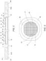
- FIG. 1illustrates a reduced plan view of an embodiment of a wafer in accordance with the present invention
- FIG. 2illustrates a cross-sectional view of the wafer of FIG. 1 mounted to a carrier substrate in accordance with an embodiment of the present invention
- FIG. 3illustrates a top view of the embodiment of FIG. 2 ;
- FIGS. 4 - 5illustrate partial cross-sectional views of the wafer of FIG. 1 at various stages in a process of singulating die from the wafer in accordance with an embodiment of the present invention
- FIG. 6illustrates a cross-sectional view of the wafer of FIG. 1 at a subsequent stage of singulation in accordance with an embodiment of the present invention
- FIG. 7illustrates an enlarged partial cross-sectional view of the embodiment of FIG. 6 in accordance with reference portion 7 - 7 ;
- FIG. 8illustrates the wafer of FIG. 1 after singulation and at a further stage of manufacture in accordance with an embodiment of the present invention.
- FIG. 9illustrates a flow chart of a batch singulation method in accordance with an embodiment of the present invention.
- the terms first, second, third and the like in the claims or/and in the Detailed Description of the Drawings, as used in a portion of a name of an elementare used for distinguishing between similar elements and not necessarily for describing a sequence, either temporally, spatially, in ranking or in any other manner. It is to be understood that the terms so used are interchangeable under appropriate circumstances and that the embodiments described herein are capable of operation in other sequences than described or illustrated herein.
- the term “major surface” when used in conjunction with a semiconductor region, wafer, or substratemeans the surface of the semiconductor region, wafer, or substrate that forms an interface with another material, such as a dielectric, an insulator, a conductor, or a polycrystalline semiconductor.
- the major surfacecan have a topography that changes in the x, y and z directions. Also, it is to be understood that where it is stated herein that one layer or region is formed on or disposed on a second layer or another region, the first layer may be formed or disposed directly on the second layer or there may be intervening layers between the first layer and the second layer. In addition, as used herein, the term formed on is used with the same meaning as located on or disposed on and is not meant to be limiting regarding any particular fabrication process.
- FIG. 1is a reduced plan view that graphically illustrates a wafer 10 at a later step in fabrication.
- wafer 10can be a semiconductor substrate.
- Wafer 10includes a plurality of semiconductor die, such as die 12 , 14 , 16 , and 18 , which are formed on or as part of semiconductor wafer 10 .
- Die 12 , 14 , 16 , and 18are spaced apart from each other on wafer 10 by spaces in which singulation lines are to be formed or defined, such as scribe lines or singulation lines 13 , 15 , 17 , and 19 .
- wafer 10As is well known in the art, all of the semiconductor die on wafer 10 generally are separated from each other on all sides by areas or spaces where scribe lines or singulation lines, such as singulation lines 13 , 15 , 17 , and 19 are to be formed. Die 12 , 14 , 16 , and 18 can be any kind of electronic device including semiconductor devices such as, diodes, transistors, discrete devices, integrated circuits, sensor devices, optical devices, or other devices known to one of ordinary skill in the art. In one embodiment, wafer 10 has completed wafer processing including the formation of a backside layer described later.
- FIG. 2illustrates an enlarged cross-sectional view of wafer 10 at an early step in a die singulation method in accordance with an embodiment.
- wafer 10is attached to a carrier substrate, transfer tape, or carrier tape 30 that facilitates supporting the plurality of die on wafer 10 after the die are singulated.
- carrier tapesare well known to those of skill in the art.
- carrier tape 30can be attached to a frame 40 , which can include frame portions or portions 401 and 402 .
- frame 40is made of a rigid material, such as stainless steel.
- carrier tape 30can be attached to surface 4010 of frame portion 401 and to surface 4020 of frame portion 402 using, for example, the adhesive side of carrier tape 30 .
- wafer 10can include a bulk substrate 11 , such as a silicon substrate, which can include opposing major surfaces 21 and 22 .
- bulk substrate 11can comprise other semiconductor materials such as heterojunction semiconductor materials or substrate 11 can be an insulating material such as ceramic materials.
- contact pads 24can be formed along, in, on, or above portions of major surface 21 to provide for electrical contact between structures formed within substrate 11 and next levels of assembly or external elements.
- contact pads 24can be formed to receive bonding wires or clips that subsequently may be attached to contact pads 24 , or contact pads 24 can be formed to receive a solder ball, bump or other type of attachment structure.
- Contact pads 24generally can be a metal or other conductive material.
- a dielectric material 26such as, a blanket deposited dielectric layer can be formed on or overlying major surface 21 to function as a passivation layer for wafer 10 .
- dielectric material 26can be a material that etches at a slower rate than that of substrate 11 .
- dielectric material 26can be a silicon oxide, silicon nitride, or polyimide when substrate 11 is silicon.
- a separate polymer protective layersuch as a patterned protective layer, can be used to protect the areas not intended to be etched during subsequent processing.
- the patterned protective layercan be a patterned photoresist layer. An example of such a protective layer is noted as element 35 in FIG. 4 described later.
- openingscan be formed in dielectric material 26 (and other dielectric layers that can be formed above or below dielectric material 26 ) to expose underlying surfaces of contact pads 24 and surfaces of substrate 11 where singulation lines 13 , 15 , 17 , and 19 are to be formed.
- the patterned photoresist layerdescribes previously can be used to form the openings with an etch process.
- wafer 10further includes a layer of material 28 formed on or overlying major surface 22 of wafer 10 .
- layer 28can be a conductive back metal layer.
- Layer 28can be any suitable conductive material appropriate for electronic technology.
- layer 28can be a multi-layer metal system such as, titanium/nickel/silver, titanium/nickel/silver/tungsten, chrome/nickel/gold, copper, copper alloys, gold, or other materials known to those skilled in the art. In some embodiments, layer 28 is greater than about one micron in thickness. In other embodiments, layer 28 is greater than about two microns in thickness. In still other embodiments, layer 28 is greater than about three microns in thickness. In another embodiment, layer 28 can be a wafer backside coating (WBC) film, such as a die-attach coating or film. In one embodiment, layer 28 can be formed having or provided with recesses, gaps, spaces, or channels between at least some adjacent die. In a further embodiment, the gaps are substantially aligned with corresponding spaces on the opposite side of wafer 10 where singulation lines 13 , 15 , 17 , 19 will be formed. In another embodiment, layer 28 is separated from the edges of least some of the die.
- WBCwafer backside coating
- FIG. 3illustrates a top view of wafer 10 in accordance with the cross-sectional view of FIG. 2 after wafer 10 has been mounted on carrier tape 30 with layer 28 against carrier tape 30 .
- carrier tape 30is mounted to frame 40 .
- frame 40can be configured with alignment portions or notches to better assist placing frame 40 into processing equipment such as the equipment described herein.
- FIG. 4illustrates an enlarged cross-sectional view of wafer 10 at a subsequent step during a singulation process in accordance with the present embodiment.
- a plasma or dry etch singulation processis illustrated. It is understood that other singulation processes can be used.
- wafer 10 mounted on carrier tape or film 30is then placed within an etch apparatus 300 , such as a plasma etch apparatus.
- substrate 11can be etched through the openings to form or define singulation lines or openings 13 , 15 , 17 , and 19 extending from major surface 21 .
- the etching processcan be performed using a chemistry (generally represented as arrows 31 ) that selectively etches silicon at a much higher rate than that of dielectrics and/or metals.
- wafer 10can be etched using a process commonly referred to as the Bosch process.
- wafer 10can be etched using the Bosch process in a deep reactive ion etch system.
- the width of singulation lines 13 , 15 , 17 , and 19can be from about five microns to about twenty microns.
- Such a widthis sufficient to ensure that the openings that form singulation lines 13 , 15 , 17 , and 19 can be formed completely through substrate 11 stopping proximate to or on layer 28 because of the etch selectivity as generally illustrated in FIG. 5 .
- layer 28can be used as a stop layer for the plasma etch singulation process.
- singulation lines 13 , 15 , 17 , and 19can be formed in about five to about thirty minutes using the Bosch process.
- a suitable etch apparatusis available from Plasma-Therm of St. Orlando, Florida, U.S.A.
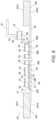
- FIG. 6illustrates a cross-sectional view of a back layer separation apparatus 60 configured to hold wafer 10 including frame 40 and carrier tape 30 .
- separation apparatus 60can be configured to process a single wafer and to provide a back layer separation process where layer 28 on wafer 10 is separated substantially at the same time (that is, batch separated) compared to other processes that separate only a localized portion of layer 28 at a time.
- separation apparatus 60can be configured to process multiple wafers each in a batch configuration.
- Apparatus 60can include a compression chamber 62 sized to accommodate wafer 10 and frame 40 depending upon the sizes of such structures.
- compression chamber 62is bounded on all sides by a plurality of generally vertical sidewalls 63 that extend generally upward from a lower chamber wall or surface 67 . Sidewalls 63 can be attached to lower chamber wall 67 using any suitable attachment devices capable of maintaining pressure with compression chamber 62 .
- Compression chamber 62further includes an upper chamber wall or surface 68 , which can include an opening 69 to accommodate a compression or pressure plate 71 or to provide an entrance for a non-compressible fluid.
- Compression chamber 62and can be any suitable shape appropriate for processing wafer 10 and frame 40 or other holding structures.
- Compression plate 71is movably associated or attached within compression chamber 62 and adapted to apply a controlled and substantially uniform pressure to wafer 10 through a pressure transfer vessel 73 containing a fluid 74 .
- vessel 73can be a fluid filled bladder that is oriented between wafer 10 and compression plate 71 .
- vessel 73comprises a cross-linked polymer material that exhibits high elastic deformation, such as a rubber or other materials as known to those of ordinary skill in the art.
- vessel 73is a static pressure balloon.
- fluid 74can be water.
- fluid 74can be water that is anaerobic (that is, water having low dissolved oxygen content or that has been deoxygenated).
- fluid 74can be heated above room temperature. In some embodiments, fluid 74 can be heated to a temperature in range from about 35 degrees Celsius to about 65 degrees Celsius. In one embodiment, fluid 74 can be heated to a temperature in range from about 45 degrees Celsius to about 55 degrees Celsius. In other embodiments, fluid 74 can be a fluid having a higher viscosity than water. In some embodiments, fluid 74 can be liquid-crystalline material. In still other embodiments, vessel 73 can be filled with a solid material, such as synthetic microspheres, carbon nanotubes, graphene, or other solid or solid-like materials that can impart or transfer pressure from compression plate 71 to carrier tape 30 without damaging wafer 10 . In some embodiments, vessel 73 can be filled with a gas.
- a solid materialsuch as synthetic microspheres, carbon nanotubes, graphene, or other solid or solid-like materials that can impart or transfer pressure from compression plate 71 to carrier tape 30 without damaging wafer 10 . In some embodiments, vessel 73 can be filled with a gas.
- vessel 73has a horizontal width proximate to wafer 10 that is larger than the horizontal width or diameter of wafer 10 to facilitate batch or near simultaneous singulation or separation of layer 28 in scribe lines 13 , 15 , 17 , and 19 of wafer 10 . That is, vessel 73 is configured or adapted to apply a pressure substantially uniformly along or across all of layer 28 and wafer 10 to provide batch separation of layer 28 in the scribe lines.
- a pressure plate 77can be detachably placed in between vessel 73 and carrier tape 30 above or in spaced relationship with wafer 10 and layer 28 .
- pressure plate 77can be a low-alloy, medium-carbon steel or high-carbon steel material with high yield strength, such as spring steel. Such a material allows pressure plate 77 to return to its original shape despite any significant bending.
- pressure plate 77can be a generally flat plate where the major surfaces lie in substantially parallel horizontal planes.
- pressure plate 77can have a lower surface (that is, the surface adjoining carrier tape 30 ) configured to first apply pressure to the outer portions of wafer 10 before or slightly before pressure applied to the more central portion of wafer 10 .
- pressure plate 77can have a slightly concave major surface adjoining carrier tape 30 without pressure applied with vessel 73 .
- pressure plate 77can have a slightly raised ridge, for example, in the shape or form of a ring around an outer periphery of pressure plate 77 .
- a protective film or protective pad 83is placed between wafer 10 and lower chamber wall 67 to protect and/or cushion wafer 10 during the separation of back layer 28 .
- protective film 83is a non-adhesive film or a low adhesive film where the adhesive strength is selected so as to minimize the occurrence of individual die being removed from carrier tape 30 after separation of back layer 28 has occurred.
- protective film 83can have a high adhesive strength (that is, higher than the adhesive strength of carrier tape 30 ) if it is desired to have the separated die adhere to protective film 83 , for example, for additional processing to the back side of wafer 10 .
- a controlled downward pressure(represented by arrows 701 and 702 ) is applied through compression plate 71 using, for example, a stepper motor driving a threaded shaft attached to compression plate 71 .
- compression plate 71can be adjusted using hydraulic or pneumatic techniques.
- compression plate 71can be adjusted manually.
- apparatus 60may include other sealing devices, fluid heating and delivery devices, and measurement and control systems that are not illustrated for the ease of understanding embodiments of the present invention. Suitable apparatus that can be configured in accordance with the description provided herein are available from Instron® of Norwood, Massachusetts, U.S.A. and Geocomp Corporation of St. Johns, New York, U.S.A.
- FIG. 7illustrates an enlarged partial cross-sectional view of a portion of apparatus 60 and wafer 10 of FIG. 6 along reference portion 7 - 7 .
- carrier tape 30is enlarged to show both a singulation film portion 301 and an adhesive film portion 302 between singulation film portion 301 and layer 28 on wafer 10 .
- singulation film portion 301can have a thickness from about 70 microns to about 90 microns and adhesive film portion 302 can have thickness from about 20 microns to about 40 microns.
- pressure applied from compression plate 71is transferred and applied through vessel 73 to optional pressure transfer plate 77 to carrier tape 30 as generally represented by arrows 701 , 702 , and 703 .
- a downward forcecan be in the range from about 700 KPa to 1400 KPa. In other embodiments, downward force can be in the range from about 1400 KPa to 3500 KPa.
- One advantage of the present methodis that it provides a batch singulation of layer 28 compared to previous processes that provide localized singulation of layer 28 . The present embodiments thus reduce manufacturing cycle time.
- Another advantageis that metal separates cleanly and self-aligned to the die edge and further, remaining material of layer 28 between die will remain on the tape after the die are removed with no need to flip the tape to expose and remove or separate the metal.
- FIG. 8illustrates a cross-sectional view of wafer 10 at a further stage of manufacturing.
- die 12 , 14 , 16 , and 18can be removed from carrier tape 30 as part of a further assembly process using, for example, a pick-and-place apparatus 81 as generally illustrated in FIG. 8 .
- portions 280 separated from layer 28remain on carrier tape 30 .
- die 12 , 14 , 16 , and 18can be attached to conductive lead frames or substrates, electrically connected to leads for traces, and encapsulated with a plastic molding compound.
- carrier tape 30can be exposed to a UV light source prior to the pick-and-place step to reduce the adhesiveness of carrier tape 30 .
- FIG. 9illustrates a flow chart for batch singulating backside material in accordance with an embodiment.
- wafer 10can be placed onto a carrier film, such as carrier tape 30 , as generally illustrated in FIG. 2 .
- wafer 10includes back layer, such as layer of material 28 .
- layer 28is a conductive metal material.
- layer 28can be a Wafer Back Coat (WBC) film, such as a die-attached coating or film.
- WBCWafer Back Coat
- materialsuch as semiconductor material, is removed from scribe lines 13 , 15 , 17 , and 19 .
- Semiconductor materialcan be removed to expose layer 28 in scribe lines 13 , 15 , 17 , and 19 , or small amount of material can be left in scribe lines 13 , 15 , 17 , and 19 . Stated another way, a sufficient amount of material is removed so that layer 28 can be effectively separated in scribe lines 13 , 15 , 17 , and 19 in a subsequent step.
- wafer 10 on carrier tape 30is placed in apparatus 60 as described with FIG. 6 .
- wafer 10is placed front side or device side down with layer 28 and carrier tape 30 facing upward.
- pressure plate 77can be placed adjacent to carrier tape 30 proximate to wafer 10 and layer 28 .
- a fluid filled vesselsuch as vessel 73
- the fluid filled vesselis filled with deoxygenated water heated to temperature from about 35 degrees Celsius to about 65 degrees Celsius.
- a pressureis applied to the fluid filled vessel using, for example, a moveable compression plate 71 as described in conjunction with FIG. 6 .
- a pressurerange from about 500 KPa to 5000 KPa can be used.
- the pressure applied to the fluid filled vesselcauses portions of the carrier film, for example, adhesive film portion 302 , to extrude into the scribe lines, such as scribe lines 13 , 15 , 17 , 19 , which batch singulates or simultaneously separates all or major portions of layer 28 from the scribe lines.
- step 903can applied multiple times (that is, more than once on the same wafer) with pressure applied, then removed, then re-applied.
- the re-applied pressurecan be greater than the previously applied pressure.
- the re-applied pressurecan be less than the previously applied pressure.
- compression plate 71can be slightly tilted and rotated to apply additional pressure around the edge regions of wafer 10 .
- compression plate 71can be rocked back and forth in multiple directions.
- a method of singulating a wafercomprises providing a wafer (for example, element 10 ) having a plurality of die (for example, elements 12 , 14 , 16 , 18 ) formed on the wafer and separated from each other by spaces, wherein the wafer has first and second opposing major surfaces (for example, elements 21 , 22 ), and wherein a layer of material (for example, element 28 ) is formed along the second major surface.
- the methodcomprises placing the wafer onto a carrier substrate (for example, element 30 ).
- the methodcomprises singulating the wafer through the spaces to form singulation lines (for example, elements 13 , 15 , 17 , 19 ), wherein singulating comprises stopping in proximity to the layer of material.
- the methodcomprises applying a pressure substantially uniformly along the second major surface to separate the layer of material in the singulation lines.
- applying the pressurecan include applying the pressure through the carrier substrate with a fluid filled vessel (for example, element 73 ) and the fluid filled vessel has a width that exceeds that of the wafer.
- the fluid filled vesselcan contain water.
- the watercan be deoxygenated.
- the methodcan further include placing a pressure plate between the fluid filled vessel and the carrier substrate, and wherein providing the wafer can comprise providing a semiconductor wafer where the layer of material comprises a conductive material, placing the wafer onto the carrier substrate can comprise placing onto a carrier tape attached to a frame, applying the pressure can comprise applying in a compression chamber, and applying the pressure can comprise a pressure from about 500 KPa to about 5000 KPa.
- the methodcan further comprise heating the wafer while applying the pressure.
- the wafercan be heated to a temperature from about 35 degrees Celsius to about 65 degrees Celsius.
- the methodcan further comprise placing a protective film proximate to the first major surface of the wafer before applying the pressure.
- a method for batch singulating a semiconductor wafercomprises providing the semiconductor wafer (for example, element 10 ) having a plurality of die (for example, elements 12 , 14 , 16 , 18 ) formed on the semiconductor wafer and separated from each other by spaces, wherein the semiconductor wafer has first and second opposing major surfaces (for example, elements 21 , 22 ), and wherein a layer of material (for example, element 28 ) is formed along the second major surface.
- the methodcomprises placing the wafer onto a carrier substrate (for example, element 30 ), wherein the layer of material is adjacent the carrier substrate.
- the methodcomprises etching the semiconductor wafer through the spaces to form singulation lines (for example, elements 13 , 15 , 17 , 19 ) and to expose portions of the layer of material in the singulation lines.
- the methodcomprises applying a pressure substantially uniformly along the second major surface of the semiconductor wafer through the carrier substrate to separate the layer of material in the singulation lines.
- applying the pressurecan include extruding portions of the carrier substrate into the singulation lines to separate the layer of material, and wherein the portions (for example, element 280 ) of the separated layer of material remain on the carrier substrate.
- applying the pressurecan include using a fluid filled vessel having a width greater than that of the semiconductor wafer.
- applying the pressurecan include using a static pressure balloon.
- the static pressure ballooncan filled with a heated fluid comprising one or more of a liquid and a gas.
- providing the semiconductor wafercan include providing the layer of material comprising a conductive material greater than about three microns in thickness, and wherein applying the pressure can comprise a pressure from about 500 KPa to about 5000 KPa.
- a method of singulating a wafercomprises providing a wafer (for example, element 10 ) having a plurality of die (for example, elements 12 , 14 , 16 , 18 ) formed on the wafer and separated from each other by spaces, wherein the wafer has first and second opposing major surfaces (for example, element s 21 , 22 ), and wherein a layer of material (for example, element 38 ) is formed along the second major surface.
- the methodcomprises placing the wafer onto a carrier substrate (for example, element 30 ) having an adhesive portion, wherein the layer of material is adjacent the carrier substrate.
- the methodseparating the wafer through the spaces to form singulation lines (for example, elements 13 , 15 , 17 , 19 ), wherein singulating lines terminate in proximity to the layer of material.
- the methodcomprises applying a pressure across the second surface of the wafer to extrude the adhesive portion into the singulation lines to separate the layer of material in the singulation lines, wherein portions (for example, element 280 ) of the separated layer of material remain on the carrier substrate.
- applying the pressurecan comprise compressing a static pressure balloon (for example, element 73 ) having a diameter greater than that of the wafer.
- applying the pressurecan comprise using a fluid filled vessel (for example, elements 73 , 74 ).
- the methodcan further comprise heating the wafer while applying the pressure.
- providing the wafercan comprise providing the layer of material having a thickness greater than about three microns and applying the pressure can comprise a pressure between about 500 KPa to about 5000 KPa.
- a method for separating a layer of material on a wafercomprises providing the wafer (for example, element 10 ) having a plurality of die (for example, element 12 , 14 , 16 , 18 ) formed on the wafer and separated from each other by singulation lines (for example, elements 13 , 15 , 17 , 19 ), wherein the wafer has first and second opposing major surfaces (for example, elements 21 , 22 ), and wherein a layer of material (for example, element 28 ) is formed along the second major surface, and wherein the singulation lines extend from the first major surface and terminate proximate to the layer of material, and wherein the wafer is attached to a carrier substrate (for example, element 30 ).
- the methodcomprises simultaneously applying a pressure along the entire second major surface of the wafer through the carrier substrate to separate the layer of material in the singulation lines.
- a novel methodis disclosed. Included, among other features, is placing a substrate having a layer of material on a major surface of the substrate onto a carrier tape, and forming singulation lines through the substrate to expose portions of the layer of material within the singulation lines.
- a pressureis substantially uniformly applied along the second major surface of the substrate through the carrier tape to separate the layer of material in the singulation lines in a batch configuration.
- the pressureis applied with a fluid filled vessel that is controllably compressed against the wafer.
- the methodprovides, among other things, an efficient, reliable, and cost effective process for batch singulating substrates that include back layers, such as thicker back metal layers or WBC layers.
- inventive aspectsmay lie in less than all features of a single foregoing disclosed embodiment.
- inventive aspectsmay lie in less than all features of a single foregoing disclosed embodiment.
- the hereinafter expressed claimsare hereby expressly incorporated into this Detailed Description of the Drawings, with each claim standing on its own as a separate embodiment of the invention.
- some embodiments described hereininclude some but not other features included in other embodiments, combinations of features of different embodiments are meant to be within the scope of the invention and meant to form different embodiments as would be understood by those skilled in the art.
Landscapes
- Engineering & Computer Science (AREA)
- Physics & Mathematics (AREA)
- Condensed Matter Physics & Semiconductors (AREA)
- General Physics & Mathematics (AREA)
- Manufacturing & Machinery (AREA)
- Computer Hardware Design (AREA)
- Microelectronics & Electronic Packaging (AREA)
- Power Engineering (AREA)
- Plasma & Fusion (AREA)
- Life Sciences & Earth Sciences (AREA)
- Forests & Forestry (AREA)
- Mechanical Engineering (AREA)
- Container, Conveyance, Adherence, Positioning, Of Wafer (AREA)
- Dicing (AREA)
- Chemical & Material Sciences (AREA)
- Chemical Kinetics & Catalysis (AREA)
- General Chemical & Material Sciences (AREA)
Abstract
Description
Claims (20)
Priority Applications (1)
| Application Number | Priority Date | Filing Date | Title |
|---|---|---|---|
| US17/248,751US12224208B2 (en) | 2014-03-21 | 2021-02-05 | Method of separating electronic devices having a back layer and apparatus |
Applications Claiming Priority (6)
| Application Number | Priority Date | Filing Date | Title |
|---|---|---|---|
| US14/222,464US9418894B2 (en) | 2014-03-21 | 2014-03-21 | Electronic die singulation method |
| US15/185,208US9589844B2 (en) | 2014-03-21 | 2016-06-17 | Electronic die singulation method |
| US15/403,676US9917013B2 (en) | 2014-03-21 | 2017-01-11 | Method of separating electronic devices having a back layer |
| US15/874,307US10446446B2 (en) | 2014-03-21 | 2018-01-18 | Method of separating electronic devices having a back layer and apparatus |
| US16/535,562US10950503B2 (en) | 2014-03-21 | 2019-08-08 | Method of separating electronic devices having a back layer and apparatus |
| US17/248,751US12224208B2 (en) | 2014-03-21 | 2021-02-05 | Method of separating electronic devices having a back layer and apparatus |
Related Parent Applications (1)
| Application Number | Title | Priority Date | Filing Date |
|---|---|---|---|
| US16/535,562DivisionUS10950503B2 (en) | 2014-03-21 | 2019-08-08 | Method of separating electronic devices having a back layer and apparatus |
Publications (2)
| Publication Number | Publication Date |
|---|---|
| US20210183705A1 US20210183705A1 (en) | 2021-06-17 |
| US12224208B2true US12224208B2 (en) | 2025-02-11 |
Family
ID=54121478
Family Applications (6)
| Application Number | Title | Priority Date | Filing Date |
|---|---|---|---|
| US14/222,464Active2034-03-27US9418894B2 (en) | 2014-03-21 | 2014-03-21 | Electronic die singulation method |
| US15/185,208ActiveUS9589844B2 (en) | 2014-03-21 | 2016-06-17 | Electronic die singulation method |
| US15/403,676ActiveUS9917013B2 (en) | 2014-03-21 | 2017-01-11 | Method of separating electronic devices having a back layer |
| US15/874,307ActiveUS10446446B2 (en) | 2014-03-21 | 2018-01-18 | Method of separating electronic devices having a back layer and apparatus |
| US16/535,562ActiveUS10950503B2 (en) | 2014-03-21 | 2019-08-08 | Method of separating electronic devices having a back layer and apparatus |
| US17/248,751Active2036-12-12US12224208B2 (en) | 2014-03-21 | 2021-02-05 | Method of separating electronic devices having a back layer and apparatus |
Family Applications Before (5)
| Application Number | Title | Priority Date | Filing Date |
|---|---|---|---|
| US14/222,464Active2034-03-27US9418894B2 (en) | 2014-03-21 | 2014-03-21 | Electronic die singulation method |
| US15/185,208ActiveUS9589844B2 (en) | 2014-03-21 | 2016-06-17 | Electronic die singulation method |
| US15/403,676ActiveUS9917013B2 (en) | 2014-03-21 | 2017-01-11 | Method of separating electronic devices having a back layer |
| US15/874,307ActiveUS10446446B2 (en) | 2014-03-21 | 2018-01-18 | Method of separating electronic devices having a back layer and apparatus |
| US16/535,562ActiveUS10950503B2 (en) | 2014-03-21 | 2019-08-08 | Method of separating electronic devices having a back layer and apparatus |
Country Status (2)
| Country | Link |
|---|---|
| US (6) | US9418894B2 (en) |
| CN (1) | CN104934374B (en) |
Families Citing this family (12)
| Publication number | Priority date | Publication date | Assignee | Title |
|---|---|---|---|---|
| US9704748B2 (en)* | 2015-06-25 | 2017-07-11 | Infineon Technologies Ag | Method of dicing a wafer |
| JP6265175B2 (en)* | 2015-06-30 | 2018-01-24 | 日亜化学工業株式会社 | Manufacturing method of semiconductor device |
| US9741617B2 (en) | 2015-11-16 | 2017-08-22 | Amkor Technology, Inc. | Encapsulated semiconductor package and method of manufacturing thereof |
| US9972575B2 (en)* | 2016-03-03 | 2018-05-15 | Applied Materials, Inc. | Hybrid wafer dicing approach using a split beam laser scribing process and plasma etch process |
| CN109075138A (en) | 2016-04-29 | 2018-12-21 | 弗莱尔系统公司 | The method of separation and encapsulation |
| JP2017212255A (en)* | 2016-05-23 | 2017-11-30 | 株式会社ジェイデバイス | Semiconductor manufacturing apparatus and manufacturing method |
| US10366923B2 (en) | 2016-06-02 | 2019-07-30 | Semiconductor Components Industries, Llc | Method of separating electronic devices having a back layer and apparatus |
| JP6906843B2 (en)* | 2017-04-28 | 2021-07-21 | 株式会社ディスコ | Wafer processing method |
| US10373869B2 (en) | 2017-05-24 | 2019-08-06 | Semiconductor Components Industries, Llc | Method of separating a back layer on a substrate using exposure to reduced temperature and related apparatus |
| CN107946251B (en)* | 2017-12-28 | 2024-02-02 | 江阴长电先进封装有限公司 | Packaging method of semiconductor product |
| KR102789194B1 (en)* | 2020-05-12 | 2025-03-28 | 삼성전자주식회사 | A semiconductor chip mounting tape and a method of manufacturing semiconductor package using the tape |
| CN115140700A (en)* | 2021-03-30 | 2022-10-04 | 诺思(天津)微系统有限责任公司 | Semiconductor assembly and cutting method thereof, filter and electronic equipment |
Citations (84)
| Publication number | Priority date | Publication date | Assignee | Title |
|---|---|---|---|---|
| US3493155A (en)* | 1969-05-05 | 1970-02-03 | Nasa | Apparatus and method for separating a semiconductor wafer |
| US3615047A (en)* | 1969-06-30 | 1971-10-26 | Bell Telephone Labor Inc | Apparatus and method for separating scribed plates of brittle material |
| US4820377A (en) | 1987-07-16 | 1989-04-11 | Texas Instruments Incorporated | Method for cleanup processing chamber and vacuum process module |
| JPH01292839A (en) | 1988-05-19 | 1989-11-27 | Mitsubishi Electric Corp | Semiconductor wafer dividing method and device |
| US5075253A (en) | 1989-04-12 | 1991-12-24 | Advanced Micro Devices, Inc. | Method of coplanar integration of semiconductor IC devices |
| US5166097A (en) | 1990-11-26 | 1992-11-24 | The Boeing Company | Silicon wafers containing conductive feedthroughs |
| US5753418A (en) | 1996-09-03 | 1998-05-19 | Taiwan Semiconductor Manufacturing Company Ltd | 0.3 Micron aperture width patterning process |
| US5856705A (en) | 1993-01-25 | 1999-01-05 | Intel Corporation | Sealed semiconductor chip and process for fabricating sealed semiconductor chip |
| US5863813A (en) | 1997-08-20 | 1999-01-26 | Micron Communications, Inc. | Method of processing semiconductive material wafers and method of forming flip chips and semiconductor chips |
| US6030885A (en) | 1997-04-18 | 2000-02-29 | Vlsi Technology, Inc. | Hexagonal semiconductor die, semiconductor substrates, and methods of forming a semiconductor die |
| US6140151A (en) | 1998-05-22 | 2000-10-31 | Micron Technology, Inc. | Semiconductor wafer processing method |
| US6165814A (en) | 1997-05-23 | 2000-12-26 | Micron Technology, Inc. | Thin film capacitor coupons for memory modules and multi-chip modules |
| US6200851B1 (en) | 1996-12-20 | 2001-03-13 | Siemens Aktiengesellschaft | Memory cell that includes a vertical transistor and a trench capacitor |
| US6214703B1 (en) | 1999-04-15 | 2001-04-10 | Taiwan Semiconductor Manufacturing Company | Method to increase wafer utility by implementing deep trench in scribe line |
| WO2001056063A2 (en) | 2000-01-26 | 2001-08-02 | Tru-Si Technologies, Inc. | Thinning and dicing of semiconductor wafers using dry etch, and obtaining semiconductor chips with rounded bottom edges and corners |
| FR2812223A1 (en)* | 2000-07-28 | 2002-02-01 | Thomson Csf | Electronic circuit substrate gluing procedure, uses conductive thermoplastic film heated and compressed between substrate and base |
| US6406979B2 (en) | 2000-06-27 | 2002-06-18 | Robert Bosch Gmbh | Method for sectioning a substrate wafer into a plurality of substrate chips |
| US6563204B1 (en) | 1999-01-20 | 2003-05-13 | Amkor Technology, Inc. | Microcircuit die-sawing protector |
| US6642127B2 (en) | 2001-10-19 | 2003-11-04 | Applied Materials, Inc. | Method for dicing a semiconductor wafer |
| US20030207579A1 (en) | 2002-05-01 | 2003-11-06 | Michael Rattner | Method of etching a deep trench having a tapered profile in silicon |
| US6686225B2 (en) | 2001-07-27 | 2004-02-03 | Texas Instruments Incorporated | Method of separating semiconductor dies from a wafer |
| US20040087062A1 (en) | 2002-03-12 | 2004-05-06 | Nec Electronics Corporation | Semiconductor device and method of manufacturing the same |
| US20040102025A1 (en) | 2002-11-20 | 2004-05-27 | Matsushita Electric Industrial Co., Ltd. | Method of manufacturing semiconductor device, plasma processing apparatus and plasma processing method |
| WO2004066382A1 (en) | 2003-01-23 | 2004-08-05 | Matsushita Electric Industrial Co., Ltd. | Method of manufacturing semiconductor device and cutting apparatus for cutting semiconductor wafer |
| US20040185580A1 (en) | 2003-03-22 | 2004-09-23 | Seok Goh | Method for dicing semiconductor wafer |
| US20050084996A1 (en) | 2001-12-21 | 2005-04-21 | Harper Ruth E. | Solid state plasma antenna |
| US6890786B2 (en)* | 2000-07-20 | 2005-05-10 | Brillian Corporation | Wafer scale processing |
| US20050101109A1 (en)* | 2003-10-27 | 2005-05-12 | Chin Oi F. | Controlled fracture substrate singulation |
| US20050104165A1 (en) | 2002-05-22 | 2005-05-19 | Sharp Kabushiki Kaisha | Semiconductor element, semiconductor device, and method for manufacturing semiconductor element |
| US20050142863A1 (en) | 2003-12-29 | 2005-06-30 | Stmicroelectronics S.R.I | Process for forming tapered trenches in a dielectric material |
| US20050196940A1 (en) | 2003-12-02 | 2005-09-08 | Koichi Yajima | Water jet processing method |
| US20060001130A1 (en) | 2002-09-25 | 2006-01-05 | Shafidul Islam | Taped lead frames and methods of making and using the same in semiconductor packaging |
| US20060030078A1 (en) | 2002-11-22 | 2006-02-09 | Tongbi Jiang | Methods of fabricating integrated circuitry |
| US20060118515A1 (en) | 2004-08-20 | 2006-06-08 | Semitool, Inc. | Process For Thinning A Semiconductor Workpiece |
| US7060531B2 (en) | 2002-12-11 | 2006-06-13 | Matsushita Electric Industrial Co., Ltd. | Method of cutting semiconductor wafer and protective sheet used in the cutting method |
| US20060143908A1 (en) | 2004-12-22 | 2006-07-06 | Pierre-Luc Duchesne | An automated dicing tool for semiconductor substrate materials |
| US20060154401A1 (en) | 2005-01-10 | 2006-07-13 | University Of Warwick | Gas-sensing semiconductor devices |
| US7098077B2 (en) | 2004-01-20 | 2006-08-29 | Taiwan Semiconductor Manufacturing Company, Ltd. | Semiconductor chip singulation method |
| US7129114B2 (en) | 2004-03-10 | 2006-10-31 | Micron Technology, Inc. | Methods relating to singulating semiconductor wafers and wafer scale assemblies |
| US20060244096A1 (en) | 2005-04-27 | 2006-11-02 | Disco Corporation | Semiconductor wafer and processing method for same |
| US20060278956A1 (en) | 2003-03-13 | 2006-12-14 | Pdf Solutions, Inc. | Semiconductor wafer with non-rectangular shaped dice |
| WO2007007883A1 (en) | 2005-07-11 | 2007-01-18 | Matsushita Electric Industrial Co., Ltd. | Manufacturing method of semiconductor devices |
| US20070087524A1 (en) | 2005-10-18 | 2007-04-19 | Robert Montgomery | Wafer singulation process |
| US20070111476A1 (en) | 2005-11-16 | 2007-05-17 | Denso Corporation | Separating device for separating semiconductor substrate and method for separating the same |
| US20070132034A1 (en) | 2005-12-14 | 2007-06-14 | Giuseppe Curello | Isolation body for semiconductor devices and method to form the same |
| US20070148807A1 (en) | 2005-08-22 | 2007-06-28 | Salman Akram | Microelectronic imagers with integrated optical devices and methods for manufacturing such microelectronic imagers |
| US7253477B2 (en) | 2005-02-15 | 2007-08-07 | Semiconductor Components Industries, L.L.C. | Semiconductor device edge termination structure |
| US20070249178A1 (en) | 2006-04-24 | 2007-10-25 | Oki Data Corporation | Semiconductor device, manufacturing method of semconductor device, manufacturing equipment of semiconductor device, light emitting diode head, and image forming apparatus |
| US20070264832A1 (en) | 2004-12-24 | 2007-11-15 | Kiyoshi Arita | Manufacturing Method For Semiconductor Chips |
| US7309623B2 (en) | 2002-01-09 | 2007-12-18 | Micron Technology, Inc. | Method of fabricating a stacked die in die BGA package |
| US7335576B2 (en) | 2004-10-08 | 2008-02-26 | Irvine Sensors Corp. | Method for precision integrated circuit die singulation using differential etch rates |
| US20080099900A1 (en) | 2006-10-31 | 2008-05-01 | Tessera Technologies Hungary Kft. | Wafer-level fabrication of lidded chips with electrodeposited dielectric coating |
| WO2008081968A1 (en) | 2006-12-26 | 2008-07-10 | Panasonic Corporation | Manufacturing method of semiconductor chip |
| US20080268619A1 (en)* | 2007-04-26 | 2008-10-30 | Disco Corporation | Wafer dividing method |
| US20090001609A1 (en) | 2005-02-28 | 2009-01-01 | Infineon Technologies Ag | Semiconductor Device and Method of Assembly |
| US7488688B2 (en) | 1999-10-25 | 2009-02-10 | Samsung Electronics Co., Ltd. | Method of removing oxide layer and semiconductor manufacturing apparatus for removing oxide layer |
| US20090057838A1 (en) | 2005-04-14 | 2009-03-05 | Panasonic Corporation | Manufacturing Method for Semiconductor Chips, and Semiconductor Chip |
| US20090061595A1 (en) | 2007-09-04 | 2009-03-05 | Infineon Technologies Ag | Method for dividing a semiconductor substrate and a method for producing a semiconductor circuit arrangement |
| US20090065904A1 (en) | 2007-09-07 | 2009-03-12 | Freescale Semiconductor, Inc. | Substrate having through-wafer vias and method of forming |
| WO2009063620A1 (en) | 2007-11-16 | 2009-05-22 | Panasonic Corporation | Plasma dicing apparatus and semiconductor chip manufacturing method |
| US20090263927A1 (en) | 2007-01-04 | 2009-10-22 | Visera Technologies Company Limited | Isolation structures for cmos image sensor chip scale packages |
| US7629228B2 (en) | 2004-08-02 | 2009-12-08 | Panasonic Corporation | Manufacturing method for semiconductor devices, and formation apparatus for semiconductor wafer dicing masks |
| US7651925B2 (en) | 2007-03-01 | 2010-01-26 | Delphi Technologies, Inc. | Vacuum expansion of integrated circuits at sort |
| US20100055875A1 (en) | 2006-08-24 | 2010-03-04 | Panasonic Corporation | Method for manufacturing semiconductor chip and method for processing semiconductor wafer |
| US7705420B2 (en) | 2004-05-05 | 2010-04-27 | Atmel Automotive Gmbh | Method for producing a conductor path on a substrate, and a component having a conductor path fabricated in accordance with such a method |
| US20100120227A1 (en) | 2007-08-07 | 2010-05-13 | Grivna Gordon M | Semiconductor die singulation method |
| US20100173474A1 (en) | 2007-02-08 | 2010-07-08 | Matsushita Electric Industrial Co., Ltd. | Method of manufacturing semiconductor chip |
| US7767551B2 (en) | 2006-10-06 | 2010-08-03 | Panasonic Corporation | Method for fabricating semiconductor chip |
| US20100197115A1 (en) | 2007-08-07 | 2010-08-05 | Panasonic Corporation | Method of segmenting semiconductor wafer |
| US7781310B2 (en) | 2007-08-07 | 2010-08-24 | Semiconductor Components Industries, Llc | Semiconductor die singulation method |
| US7846848B2 (en) | 2005-01-08 | 2010-12-07 | Applied Materials, Inc. | Cluster tool with integrated metrology chamber for transparent substrates |
| US7883343B1 (en) | 2003-04-10 | 2011-02-08 | Sunpower Corporation | Method of manufacturing solar cell |
| US20110175209A1 (en) | 2010-01-18 | 2011-07-21 | Seddon Michael J | Method of forming an em protected semiconductor die |
| US20110177675A1 (en) | 2010-01-18 | 2011-07-21 | Grivna Gordon M | Method of forming a semiconductor die |
| US20110175225A1 (en) | 2010-01-18 | 2011-07-21 | Seddon Michael J | Method of forming an em protected semiconductor die |
| US7989319B2 (en) | 2007-08-07 | 2011-08-02 | Semiconductor Components Industries, Llc | Semiconductor die singulation method |
| US20110194053A1 (en)* | 2004-05-21 | 2011-08-11 | Tannas Lawrence E | Apparatus and methods for cutting electronic displays during resizing |
| US20110244657A1 (en)* | 2007-08-07 | 2011-10-06 | Grivna Gordon M | Semiconductor die singulation method |
| US8178372B2 (en) | 2005-09-30 | 2012-05-15 | Osram Opto Semiconductors Gmbh | Method for production of a plurality of semiconductor chips, and a semiconductor component |
| US20120196426A1 (en) | 2011-02-01 | 2012-08-02 | Samsung Electronics Co., Ltd. | Wafer dicing press and method and semiconductor wafer dicing system including the same |
| US8384231B2 (en) | 2010-01-18 | 2013-02-26 | Semiconductor Components Industries, Llc | Method of forming a semiconductor die |
| US8450188B1 (en) | 2011-08-02 | 2013-05-28 | Micro Processing Technology, Inc. | Method of removing back metal from an etched semiconductor scribe street |
| US8906745B1 (en)* | 2013-09-12 | 2014-12-09 | Micro Processing Technology, Inc. | Method using fluid pressure to remove back metal from semiconductor wafer scribe streets |
| US9153493B1 (en) | 2013-01-16 | 2015-10-06 | Micro Processing Technology, Inc. | System for separating devices from a semiconductor wafer |
Family Cites Families (6)
| Publication number | Priority date | Publication date | Assignee | Title |
|---|---|---|---|---|
| KR100611064B1 (en)* | 2004-07-15 | 2006-08-10 | 삼성전자주식회사 | A slurry composition for a chemical mechanical polishing process, a chemical mechanical polishing method using the slurry composition, and a method of forming a gate pattern using the method |
| US20070011147A1 (en)* | 2005-06-22 | 2007-01-11 | Affiniti, Inc. | Systems and methods for retrieving data |
| KR101160166B1 (en)* | 2008-11-05 | 2012-06-28 | 세메스 주식회사 | Trasferring unit for scribing apparatus, cutting apparatus having the same and method of cutting substrate using the same |
| CN201540885U (en)* | 2009-11-16 | 2010-08-04 | 正文电子(苏州)有限公司 | Air compressing apparatus |
| TW201241903A (en)* | 2011-04-15 | 2012-10-16 | Lextar Electronics Corp | Die breaking process |
| US8664089B1 (en)* | 2012-08-20 | 2014-03-04 | Semiconductor Components Industries, Llc | Semiconductor die singulation method |
- 2014
- 2014-03-21USUS14/222,464patent/US9418894B2/enactiveActive
- 2014-12-18CNCN201410790910.4Apatent/CN104934374B/enactiveActive
- 2016
- 2016-06-17USUS15/185,208patent/US9589844B2/enactiveActive
- 2017
- 2017-01-11USUS15/403,676patent/US9917013B2/enactiveActive
- 2018
- 2018-01-18USUS15/874,307patent/US10446446B2/enactiveActive
- 2019
- 2019-08-08USUS16/535,562patent/US10950503B2/enactiveActive
- 2021
- 2021-02-05USUS17/248,751patent/US12224208B2/enactiveActive
Patent Citations (97)
| Publication number | Priority date | Publication date | Assignee | Title |
|---|---|---|---|---|
| US3493155A (en)* | 1969-05-05 | 1970-02-03 | Nasa | Apparatus and method for separating a semiconductor wafer |
| US3615047A (en)* | 1969-06-30 | 1971-10-26 | Bell Telephone Labor Inc | Apparatus and method for separating scribed plates of brittle material |
| US4820377A (en) | 1987-07-16 | 1989-04-11 | Texas Instruments Incorporated | Method for cleanup processing chamber and vacuum process module |
| JPH01292839A (en) | 1988-05-19 | 1989-11-27 | Mitsubishi Electric Corp | Semiconductor wafer dividing method and device |
| US5075253A (en) | 1989-04-12 | 1991-12-24 | Advanced Micro Devices, Inc. | Method of coplanar integration of semiconductor IC devices |
| US5166097A (en) | 1990-11-26 | 1992-11-24 | The Boeing Company | Silicon wafers containing conductive feedthroughs |
| US5510655A (en) | 1990-11-26 | 1996-04-23 | The Boeing Company | Silicon wafers containing conductive feedthroughs |
| US5856705A (en) | 1993-01-25 | 1999-01-05 | Intel Corporation | Sealed semiconductor chip and process for fabricating sealed semiconductor chip |
| US5753418A (en) | 1996-09-03 | 1998-05-19 | Taiwan Semiconductor Manufacturing Company Ltd | 0.3 Micron aperture width patterning process |
| US6200851B1 (en) | 1996-12-20 | 2001-03-13 | Siemens Aktiengesellschaft | Memory cell that includes a vertical transistor and a trench capacitor |
| US6030885A (en) | 1997-04-18 | 2000-02-29 | Vlsi Technology, Inc. | Hexagonal semiconductor die, semiconductor substrates, and methods of forming a semiconductor die |
| US6165814A (en) | 1997-05-23 | 2000-12-26 | Micron Technology, Inc. | Thin film capacitor coupons for memory modules and multi-chip modules |
| US6342724B1 (en) | 1997-05-23 | 2002-01-29 | Micron Technology, Inc. | Thin film capacitor coupons for memory modules and multi-chip modules |
| US5863813A (en) | 1997-08-20 | 1999-01-26 | Micron Communications, Inc. | Method of processing semiconductive material wafers and method of forming flip chips and semiconductor chips |
| US6140151A (en) | 1998-05-22 | 2000-10-31 | Micron Technology, Inc. | Semiconductor wafer processing method |
| US6563204B1 (en) | 1999-01-20 | 2003-05-13 | Amkor Technology, Inc. | Microcircuit die-sawing protector |
| US6214703B1 (en) | 1999-04-15 | 2001-04-10 | Taiwan Semiconductor Manufacturing Company | Method to increase wafer utility by implementing deep trench in scribe line |
| US7488688B2 (en) | 1999-10-25 | 2009-02-10 | Samsung Electronics Co., Ltd. | Method of removing oxide layer and semiconductor manufacturing apparatus for removing oxide layer |
| WO2001056063A3 (en) | 2000-01-26 | 2002-01-03 | Tru Si Technologies Inc | Thinning and dicing of semiconductor wafers using dry etch, and obtaining semiconductor chips with rounded bottom edges and corners |
| WO2001056063A2 (en) | 2000-01-26 | 2001-08-02 | Tru-Si Technologies, Inc. | Thinning and dicing of semiconductor wafers using dry etch, and obtaining semiconductor chips with rounded bottom edges and corners |
| US6406979B2 (en) | 2000-06-27 | 2002-06-18 | Robert Bosch Gmbh | Method for sectioning a substrate wafer into a plurality of substrate chips |
| US6890786B2 (en)* | 2000-07-20 | 2005-05-10 | Brillian Corporation | Wafer scale processing |
| FR2812223A1 (en)* | 2000-07-28 | 2002-02-01 | Thomson Csf | Electronic circuit substrate gluing procedure, uses conductive thermoplastic film heated and compressed between substrate and base |
| US6686225B2 (en) | 2001-07-27 | 2004-02-03 | Texas Instruments Incorporated | Method of separating semiconductor dies from a wafer |
| US6642127B2 (en) | 2001-10-19 | 2003-11-04 | Applied Materials, Inc. | Method for dicing a semiconductor wafer |
| US20050084996A1 (en) | 2001-12-21 | 2005-04-21 | Harper Ruth E. | Solid state plasma antenna |
| US7309623B2 (en) | 2002-01-09 | 2007-12-18 | Micron Technology, Inc. | Method of fabricating a stacked die in die BGA package |
| US20040087062A1 (en) | 2002-03-12 | 2004-05-06 | Nec Electronics Corporation | Semiconductor device and method of manufacturing the same |
| US20030207579A1 (en) | 2002-05-01 | 2003-11-06 | Michael Rattner | Method of etching a deep trench having a tapered profile in silicon |
| US20050104165A1 (en) | 2002-05-22 | 2005-05-19 | Sharp Kabushiki Kaisha | Semiconductor element, semiconductor device, and method for manufacturing semiconductor element |
| US20060001130A1 (en) | 2002-09-25 | 2006-01-05 | Shafidul Islam | Taped lead frames and methods of making and using the same in semiconductor packaging |
| US20040102025A1 (en) | 2002-11-20 | 2004-05-27 | Matsushita Electric Industrial Co., Ltd. | Method of manufacturing semiconductor device, plasma processing apparatus and plasma processing method |
| US6897128B2 (en) | 2002-11-20 | 2005-05-24 | Matsushita Electric Industrial Co., Ltd. | Method of manufacturing semiconductor device, plasma processing apparatus and plasma processing method |
| US20060030078A1 (en) | 2002-11-22 | 2006-02-09 | Tongbi Jiang | Methods of fabricating integrated circuitry |
| US7060531B2 (en) | 2002-12-11 | 2006-06-13 | Matsushita Electric Industrial Co., Ltd. | Method of cutting semiconductor wafer and protective sheet used in the cutting method |
| US6969669B2 (en) | 2003-01-23 | 2005-11-29 | Matsushita Electric Industrial Co., Ltd. | Method of manufacturing semiconductor device and cutting apparatus for cutting semiconductor wafer |
| WO2004066382A1 (en) | 2003-01-23 | 2004-08-05 | Matsushita Electric Industrial Co., Ltd. | Method of manufacturing semiconductor device and cutting apparatus for cutting semiconductor wafer |
| US20050072766A1 (en) | 2003-01-23 | 2005-04-07 | Matsushita Electric Industrial Co., Ltd. | Method of manufacturing semiconductor device and cutting apparatus for cutting semiconductor wafer |
| US20060278956A1 (en) | 2003-03-13 | 2006-12-14 | Pdf Solutions, Inc. | Semiconductor wafer with non-rectangular shaped dice |
| US20040185580A1 (en) | 2003-03-22 | 2004-09-23 | Seok Goh | Method for dicing semiconductor wafer |
| US7883343B1 (en) | 2003-04-10 | 2011-02-08 | Sunpower Corporation | Method of manufacturing solar cell |
| US20050101109A1 (en)* | 2003-10-27 | 2005-05-12 | Chin Oi F. | Controlled fracture substrate singulation |
| US20050196940A1 (en) | 2003-12-02 | 2005-09-08 | Koichi Yajima | Water jet processing method |
| US20050142863A1 (en) | 2003-12-29 | 2005-06-30 | Stmicroelectronics S.R.I | Process for forming tapered trenches in a dielectric material |
| US7098077B2 (en) | 2004-01-20 | 2006-08-29 | Taiwan Semiconductor Manufacturing Company, Ltd. | Semiconductor chip singulation method |
| US7129114B2 (en) | 2004-03-10 | 2006-10-31 | Micron Technology, Inc. | Methods relating to singulating semiconductor wafers and wafer scale assemblies |
| US7705420B2 (en) | 2004-05-05 | 2010-04-27 | Atmel Automotive Gmbh | Method for producing a conductor path on a substrate, and a component having a conductor path fabricated in accordance with such a method |
| US20110194053A1 (en)* | 2004-05-21 | 2011-08-11 | Tannas Lawrence E | Apparatus and methods for cutting electronic displays during resizing |
| US7629228B2 (en) | 2004-08-02 | 2009-12-08 | Panasonic Corporation | Manufacturing method for semiconductor devices, and formation apparatus for semiconductor wafer dicing masks |
| US20060118515A1 (en) | 2004-08-20 | 2006-06-08 | Semitool, Inc. | Process For Thinning A Semiconductor Workpiece |
| US7335576B2 (en) | 2004-10-08 | 2008-02-26 | Irvine Sensors Corp. | Method for precision integrated circuit die singulation using differential etch rates |
| US20060143908A1 (en) | 2004-12-22 | 2006-07-06 | Pierre-Luc Duchesne | An automated dicing tool for semiconductor substrate materials |
| US7678670B2 (en) | 2004-12-24 | 2010-03-16 | Panasonic Corporation | TEG removing method in manufacturing method for semiconductor chips |
| US20070264832A1 (en) | 2004-12-24 | 2007-11-15 | Kiyoshi Arita | Manufacturing Method For Semiconductor Chips |
| US7846848B2 (en) | 2005-01-08 | 2010-12-07 | Applied Materials, Inc. | Cluster tool with integrated metrology chamber for transparent substrates |
| US20060154401A1 (en) | 2005-01-10 | 2006-07-13 | University Of Warwick | Gas-sensing semiconductor devices |
| US7253477B2 (en) | 2005-02-15 | 2007-08-07 | Semiconductor Components Industries, L.L.C. | Semiconductor device edge termination structure |
| US20090001609A1 (en) | 2005-02-28 | 2009-01-01 | Infineon Technologies Ag | Semiconductor Device and Method of Assembly |
| US20090057838A1 (en) | 2005-04-14 | 2009-03-05 | Panasonic Corporation | Manufacturing Method for Semiconductor Chips, and Semiconductor Chip |
| US20060244096A1 (en) | 2005-04-27 | 2006-11-02 | Disco Corporation | Semiconductor wafer and processing method for same |
| WO2007007883A1 (en) | 2005-07-11 | 2007-01-18 | Matsushita Electric Industrial Co., Ltd. | Manufacturing method of semiconductor devices |
| US20090209087A1 (en) | 2005-07-11 | 2009-08-20 | Matsushita Electric Industrial Co., Ltd. | Manufacturing method of semiconductor devices |
| US20070148807A1 (en) | 2005-08-22 | 2007-06-28 | Salman Akram | Microelectronic imagers with integrated optical devices and methods for manufacturing such microelectronic imagers |
| US8178372B2 (en) | 2005-09-30 | 2012-05-15 | Osram Opto Semiconductors Gmbh | Method for production of a plurality of semiconductor chips, and a semiconductor component |
| US20070087524A1 (en) | 2005-10-18 | 2007-04-19 | Robert Montgomery | Wafer singulation process |
| US20070111476A1 (en) | 2005-11-16 | 2007-05-17 | Denso Corporation | Separating device for separating semiconductor substrate and method for separating the same |
| US20070132034A1 (en) | 2005-12-14 | 2007-06-14 | Giuseppe Curello | Isolation body for semiconductor devices and method to form the same |
| US20070249178A1 (en) | 2006-04-24 | 2007-10-25 | Oki Data Corporation | Semiconductor device, manufacturing method of semconductor device, manufacturing equipment of semiconductor device, light emitting diode head, and image forming apparatus |
| US20100055875A1 (en) | 2006-08-24 | 2010-03-04 | Panasonic Corporation | Method for manufacturing semiconductor chip and method for processing semiconductor wafer |
| US7767551B2 (en) | 2006-10-06 | 2010-08-03 | Panasonic Corporation | Method for fabricating semiconductor chip |
| US20080099900A1 (en) | 2006-10-31 | 2008-05-01 | Tessera Technologies Hungary Kft. | Wafer-level fabrication of lidded chips with electrodeposited dielectric coating |
| WO2008081968A1 (en) | 2006-12-26 | 2008-07-10 | Panasonic Corporation | Manufacturing method of semiconductor chip |
| US20090263927A1 (en) | 2007-01-04 | 2009-10-22 | Visera Technologies Company Limited | Isolation structures for cmos image sensor chip scale packages |
| US7906410B2 (en) | 2007-02-08 | 2011-03-15 | Panasonic Corporation | Method of manufacturing semiconductor chip using laser light and plasma dicing |
| US20100173474A1 (en) | 2007-02-08 | 2010-07-08 | Matsushita Electric Industrial Co., Ltd. | Method of manufacturing semiconductor chip |
| US7651925B2 (en) | 2007-03-01 | 2010-01-26 | Delphi Technologies, Inc. | Vacuum expansion of integrated circuits at sort |
| US20080268619A1 (en)* | 2007-04-26 | 2008-10-30 | Disco Corporation | Wafer dividing method |
| US7989319B2 (en) | 2007-08-07 | 2011-08-02 | Semiconductor Components Industries, Llc | Semiconductor die singulation method |
| US20100197115A1 (en) | 2007-08-07 | 2010-08-05 | Panasonic Corporation | Method of segmenting semiconductor wafer |
| US20100120227A1 (en) | 2007-08-07 | 2010-05-13 | Grivna Gordon M | Semiconductor die singulation method |
| US20120244681A1 (en) | 2007-08-07 | 2012-09-27 | Grivna Gordon M | Semiconductor die singulation method |
| US20110244657A1 (en)* | 2007-08-07 | 2011-10-06 | Grivna Gordon M | Semiconductor die singulation method |
| US8012857B2 (en) | 2007-08-07 | 2011-09-06 | Semiconductor Components Industries, Llc | Semiconductor die singulation method |
| US7985661B2 (en) | 2007-08-07 | 2011-07-26 | Semiconductor Components Industries, Llc | Semiconductor die singulation method |
| US7781310B2 (en) | 2007-08-07 | 2010-08-24 | Semiconductor Components Industries, Llc | Semiconductor die singulation method |
| US20090061595A1 (en) | 2007-09-04 | 2009-03-05 | Infineon Technologies Ag | Method for dividing a semiconductor substrate and a method for producing a semiconductor circuit arrangement |
| US20090065904A1 (en) | 2007-09-07 | 2009-03-12 | Freescale Semiconductor, Inc. | Substrate having through-wafer vias and method of forming |
| WO2009063620A1 (en) | 2007-11-16 | 2009-05-22 | Panasonic Corporation | Plasma dicing apparatus and semiconductor chip manufacturing method |
| US20100048001A1 (en) | 2007-11-16 | 2010-02-25 | Atsushi Harikai | Plasma dicing apparatus and method of manufacturing semiconductor chips |
| US20110175225A1 (en) | 2010-01-18 | 2011-07-21 | Seddon Michael J | Method of forming an em protected semiconductor die |
| US20110177675A1 (en) | 2010-01-18 | 2011-07-21 | Grivna Gordon M | Method of forming a semiconductor die |
| US20110175209A1 (en) | 2010-01-18 | 2011-07-21 | Seddon Michael J | Method of forming an em protected semiconductor die |
| US8384231B2 (en) | 2010-01-18 | 2013-02-26 | Semiconductor Components Industries, Llc | Method of forming a semiconductor die |
| US20120196426A1 (en) | 2011-02-01 | 2012-08-02 | Samsung Electronics Co., Ltd. | Wafer dicing press and method and semiconductor wafer dicing system including the same |
| US8450188B1 (en) | 2011-08-02 | 2013-05-28 | Micro Processing Technology, Inc. | Method of removing back metal from an etched semiconductor scribe street |
| US9153493B1 (en) | 2013-01-16 | 2015-10-06 | Micro Processing Technology, Inc. | System for separating devices from a semiconductor wafer |
| US8906745B1 (en)* | 2013-09-12 | 2014-12-09 | Micro Processing Technology, Inc. | Method using fluid pressure to remove back metal from semiconductor wafer scribe streets |
Non-Patent Citations (9)
| Title |
|---|
| Earl N. Taylor, Examiner, United States Patent and Trademark Office, "Petition Decision", dated Feb. 1, 2018. |
| ON Semiconductor and Micro Processing Technology, Inc.; Petition to Correct Inventorship of a Patent and Request for Certificate of Correction Under 37 CFR 1.324; filed Nov. 21, 2017 with the USPTO for U.S. Pat. No. 8,906,745 to add inventor Gordon M. Grivna. |
| ON Semiconductor Corporation et al. v. Micro Processing Technology, Inc.; Complaint involving U.S. Pat. Nos. 8,450,188, 9,153,493, 8,906,745, for correction of inventorship, breach of contract, and trade secret misappropriation; Case No. 2:16-cv-01055-DLR; US District Court for the District of Arizona; Filed Apr. 14, 2016. |
| ON Semiconductor Corporation et al. v. Micro Processing Technology, Inc.; First Amended Complaint involving U.S. Pat. Nos. 8,450,188, 9,153,493, 8,906,745, for correction of inventorship, breach of contract, and trade secret misappropriation; Case No. 2:16-cv-01055-DLR; US District Court for the District of Arizona; Filed Jun. 15, 2016. |
| ON Semiconductor Corporation et al. v. Micro Processing Technology, Inc.; Joint Stipulation of Dismissal with Prejudice; request by both parties to dismiss Case No. Case No. 8:17-cv-00322-T-CEH-JSS; US District Court Middle District of Florida Tampa Division with prejudice; Filed Nov. 20, 2017 within the 60 day limit set by the Sep. 19, 2017 Order issued by Judge Honeywell. |
| ON Semiconductor Corporation et al. v. Micro Processing Technology, Inc.; Order to Dismiss for Case No. 8:17-cv-00322-T-CEH-JSS; US District Court Middle District of Florida Tampa Division; issued on Sep. 19, 2017 by Judge Honeywell. |
| ON Semiconductor Corporation et al. v. Micro Processing Technology, Inc.; Second Amended Complaint involving U.S. Pat. Nos. 8,450,188, 9,153, 493, 8,906,745, for correction of inventorship, breach of contract, and trade secret misappropriation; Case No. 8:17-cv-00322-T-CEH-JSS; US District Court Middle District of Florida Tampa Division; Filed Mar. 14, 2017. |
| Report on the Filing or Determination of an Action Regarding a Patent or Trademark in Compliance with 35 U.S.C. 290; Docket 2:16-cv-01055-DLR; Filed Apr. 14, 2016 for U.S. Pat. Nos. 8,450,188; 9,153,493; and 8,906,745. |
| United States Patent and Trademark Office "Certificate of Correction", U.S. Appl. No. 14/273,755, filed May 9, 2014; U.S. Pat. No. 8,906,745, granted Dec. 9, 2014. |
Also Published As
| Publication number | Publication date |
|---|---|
| US20190363019A1 (en) | 2019-11-28 |
| US10446446B2 (en) | 2019-10-15 |
| US9589844B2 (en) | 2017-03-07 |
| US10950503B2 (en) | 2021-03-16 |
| US9418894B2 (en) | 2016-08-16 |
| US20180158734A1 (en) | 2018-06-07 |
| US20160293488A1 (en) | 2016-10-06 |
| CN104934374B (en) | 2019-08-06 |
| US20210183705A1 (en) | 2021-06-17 |
| US9917013B2 (en) | 2018-03-13 |
| US20170125294A1 (en) | 2017-05-04 |
| US20150270173A1 (en) | 2015-09-24 |
| CN104934374A (en) | 2015-09-23 |
Similar Documents
| Publication | Publication Date | Title |
|---|---|---|
| US12224208B2 (en) | Method of separating electronic devices having a back layer and apparatus | |
| US10770350B2 (en) | Method of separating a back layer on a singulated semiconductor wafer attached to carrier substrate | |
| US8664089B1 (en) | Semiconductor die singulation method | |
| US9773689B2 (en) | Semiconductor die singulation method using varied carrier substrate temperature | |
| US10796961B2 (en) | Method of separating electronic devices having a back layer and apparatus | |
| US9847219B2 (en) | Semiconductor die singulation method |
Legal Events
| Date | Code | Title | Description |
|---|---|---|---|
| AS | Assignment | Owner name:SEMICONDUCTOR COMPONENTS INDUSTRIES, LLC, ARIZONA Free format text:ASSIGNMENT OF ASSIGNORS INTEREST;ASSIGNOR:GRIVNA, GORDON M.;REEL/FRAME:055164/0874 Effective date:20140321 | |
| FEPP | Fee payment procedure | Free format text:ENTITY STATUS SET TO UNDISCOUNTED (ORIGINAL EVENT CODE: BIG.); ENTITY STATUS OF PATENT OWNER: LARGE ENTITY | |
| STPP | Information on status: patent application and granting procedure in general | Free format text:APPLICATION DISPATCHED FROM PREEXAM, NOT YET DOCKETED | |
| AS | Assignment | Owner name:DEUTSCHE BANK AG NEW YORK BRANCH, AS COLLATERAL AGENT, NEW YORK Free format text:SECURITY INTEREST;ASSIGNOR:SEMICONDUCTOR COMPONENTS INDUSTRIES, LLC;REEL/FRAME:056595/0177 Effective date:20210506 | |
| STPP | Information on status: patent application and granting procedure in general | Free format text:DOCKETED NEW CASE - READY FOR EXAMINATION | |
| AS | Assignment | Owner name:SEMICONDUCTOR COMPONENTS INDUSTRIES, LLC, ARIZONA Free format text:RELEASE OF SECURITY INTEREST IN PATENTS PREVIOUSLY RECORDED AT REEL 056595, FRAME 0177;ASSIGNOR:DEUTSCHE BANK AG NEW YORK BRANCH, AS COLLATERAL AGENT;REEL/FRAME:064615/0564 Effective date:20230816 | |
| STPP | Information on status: patent application and granting procedure in general | Free format text:NON FINAL ACTION MAILED | |
| STPP | Information on status: patent application and granting procedure in general | Free format text:RESPONSE TO NON-FINAL OFFICE ACTION ENTERED AND FORWARDED TO EXAMINER | |
| STPP | Information on status: patent application and granting procedure in general | Free format text:NOTICE OF ALLOWANCE MAILED -- APPLICATION RECEIVED IN OFFICE OF PUBLICATIONS | |
| STPP | Information on status: patent application and granting procedure in general | Free format text:PUBLICATIONS -- ISSUE FEE PAYMENT VERIFIED | |
| STCF | Information on status: patent grant | Free format text:PATENTED CASE |