US12216277B2 - Optical element for deconvolution - Google Patents
Optical element for deconvolutionDownload PDFInfo
- Publication number
- US12216277B2 US12216277B2US17/963,609US202217963609AUS12216277B2US 12216277 B2US12216277 B2US 12216277B2US 202217963609 AUS202217963609 AUS 202217963609AUS 12216277 B2US12216277 B2US 12216277B2
- Authority
- US
- United States
- Prior art keywords
- optical element
- field
- image
- display
- wavelengths
- Prior art date
- Legal status (The legal status is an assumption and is not a legal conclusion. Google has not performed a legal analysis and makes no representation as to the accuracy of the status listed.)
- Active, expires
Links
Images


Classifications
- H—ELECTRICITY
- H04—ELECTRIC COMMUNICATION TECHNIQUE
- H04N—PICTORIAL COMMUNICATION, e.g. TELEVISION
- H04N23/00—Cameras or camera modules comprising electronic image sensors; Control thereof
- H04N23/95—Computational photography systems, e.g. light-field imaging systems
- G—PHYSICS
- G02—OPTICS
- G02B—OPTICAL ELEMENTS, SYSTEMS OR APPARATUS
- G02B26/00—Optical devices or arrangements for the control of light using movable or deformable optical elements
- G02B26/06—Optical devices or arrangements for the control of light using movable or deformable optical elements for controlling the phase of light
- G—PHYSICS
- G02—OPTICS
- G02B—OPTICAL ELEMENTS, SYSTEMS OR APPARATUS
- G02B27/00—Optical systems or apparatus not provided for by any of the groups G02B1/00 - G02B26/00, G02B30/00
- G02B27/0025—Optical systems or apparatus not provided for by any of the groups G02B1/00 - G02B26/00, G02B30/00 for optical correction, e.g. distorsion, aberration
- G02B27/0068—Optical systems or apparatus not provided for by any of the groups G02B1/00 - G02B26/00, G02B30/00 for optical correction, e.g. distorsion, aberration having means for controlling the degree of correction, e.g. using phase modulators, movable elements
- G—PHYSICS
- G02—OPTICS
- G02B—OPTICAL ELEMENTS, SYSTEMS OR APPARATUS
- G02B5/00—Optical elements other than lenses
- G02B5/18—Diffraction gratings
- G02B5/1866—Transmission gratings characterised by their structure, e.g. step profile, contours of substrate or grooves, pitch variations, materials
- G02B5/1871—Transmissive phase gratings
- G—PHYSICS
- G06—COMPUTING OR CALCULATING; COUNTING
- G06T—IMAGE DATA PROCESSING OR GENERATION, IN GENERAL
- G06T5/00—Image enhancement or restoration
- G06T5/20—Image enhancement or restoration using local operators
- G—PHYSICS
- G06—COMPUTING OR CALCULATING; COUNTING
- G06T—IMAGE DATA PROCESSING OR GENERATION, IN GENERAL
- G06T5/00—Image enhancement or restoration
- G06T5/73—Deblurring; Sharpening
- H—ELECTRICITY
- H04—ELECTRIC COMMUNICATION TECHNIQUE
- H04N—PICTORIAL COMMUNICATION, e.g. TELEVISION
- H04N23/00—Cameras or camera modules comprising electronic image sensors; Control thereof
- H04N23/50—Constructional details
- H04N23/53—Constructional details of electronic viewfinders, e.g. rotatable or detachable
- H—ELECTRICITY
- H04—ELECTRIC COMMUNICATION TECHNIQUE
- H04N—PICTORIAL COMMUNICATION, e.g. TELEVISION
- H04N23/00—Cameras or camera modules comprising electronic image sensors; Control thereof
- H04N23/50—Constructional details
- H04N23/55—Optical parts specially adapted for electronic image sensors; Mounting thereof
- G—PHYSICS
- G02—OPTICS
- G02B—OPTICAL ELEMENTS, SYSTEMS OR APPARATUS
- G02B1/00—Optical elements characterised by the material of which they are made; Optical coatings for optical elements
- G02B1/002—Optical elements characterised by the material of which they are made; Optical coatings for optical elements made of materials engineered to provide properties not available in nature, e.g. metamaterials
- G—PHYSICS
- G02—OPTICS
- G02B—OPTICAL ELEMENTS, SYSTEMS OR APPARATUS
- G02B5/00—Optical elements other than lenses
- G02B5/32—Holograms used as optical elements
- G—PHYSICS
- G06—COMPUTING OR CALCULATING; COUNTING
- G06T—IMAGE DATA PROCESSING OR GENERATION, IN GENERAL
- G06T2207/00—Indexing scheme for image analysis or image enhancement
- G06T2207/20—Special algorithmic details
- G06T2207/20021—Dividing image into blocks, subimages or windows
- G—PHYSICS
- G06—COMPUTING OR CALCULATING; COUNTING
- G06T—IMAGE DATA PROCESSING OR GENERATION, IN GENERAL
- G06T2207/00—Indexing scheme for image analysis or image enhancement
- G06T2207/20—Special algorithmic details
- G06T2207/20212—Image combination
Definitions
- This applicationgenerally relates to an optical element for performing deconvolution.
- FIG. 2illustrates an example method for creating an optical element that performs deconvolution.
- FIG. 4illustrates an example optical response of a system using an example optical element that performs deconvolution.
- FIG. 5illustrates an example computing device.
- Images captured by an image sensor of an electronic devicemay be blurred for a variety of reasons.
- a front-facing cameramay be disposed under a display (or another surface) of a personal electronic device, for example to decrease the camera's footprint on the surface of the device and to increase the useable surface of the device.
- placing a front-facing camera behind a display of an electronic devicemay increase the size of the device's display.
- disposing the front-facing camera system behind the display panelmay degrade images captured by the front-facing camera, for example because of interference caused by the display structure as light passes through the display to the camera sensor, as described more fully below.
- One or more PSF measurementscan be performed to characterize the degradation of an image captured by an image sensor, such as an under-display camera.
- Each PSFmay be a function of the source's wavelength, distance, and angle with the optical axis with respect to the camera's sensor.
- the set of PSFsare then used to reconstruct an undegraded image via deconvolution, for example by convolving the blurred image with the inverse PSFs.
- the deconvolutionis typically performed as a computational, numerical process by a computing device, such as by a processor of a computing device. Deconvolution calculations consume system resources, such as power, memory, and available processing capabilities, and for a device to perform deconvolution computationally the device must have the minimum capabilities, such as processing capabilities, necessary to perform the computations.
- embodiments of this disclosureperform deconvolution in the optical domain by using one or more physical optical elements designed to deblur images.
- the physical optical elementoptically performs deconvolution by manipulating the light that reaches a camera's sensor, and therefore requires little or no computation to be performed by the device in order to de-blur an image.
- Embodiments of this disclosuretherefore reduce systems cost, computational requirements, power budget, and the time required for image reconstruction.
- embodiments discloses hereinenable deconvolution techniques to be performed by lightweight devices that do not have the computational resources necessary to perform deconvolution.
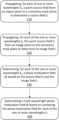
- FIG. 1illustrates an example system including a corrective optical element that performs deconvolution.
- source 110which may be a point source or may represent a point source, lies in an object plane and creates optical source field S.
- source field Smay be incoherent light comprised of many different wavelengths, e.g., wavelengths in the visible spectrum.
- Source field Sarrives at, and is modified by, mask 120 , which for example represents the layers of a physical display screen, for example a display screen of a personal electronic device, such as a mobile phone, tablet computer, smartwatch, camera, laptop, monitor, television, and so forth As shown in the example of FIG.
- source field Spasses through a transparent portion of the display screen and may interact with one or more optical components 130 .
- optical components 130may include one or more lenses, which may be part of a camera system, that collect and focus light. While the example of FIG. 1 illustrates a single optical component 130 , this disclosure contemplates that more than one optical component 130 may be present, and moreover that in some embodiments all or some optical components may be disposed prior to corrective mask 140 while in some embodiments all or some optical components may be disposed after corrective mask 140 .
- corrective mask 140also referred to herein as an “optical element” or “corrective optical element”.
- Corrective mask 140interacts with and modifies source field S so that the optical field emerging from corrective element 140 is image field I.
- corrective mask 140deconvolves the blurring introduced to source field S, e.g., by the display structure represented by mask 120 .
- the resulting image field Irepresents a de-blurred image field, and as shown in the example of FIG. 1 , de-blurred image field I is captured by image sensor 150 , for example an image sensor of a camera.
- image sensor 150for example an image sensor of a camera.
- FIG. 1relates to deconvolving an image captured by a camera that is mounted under a display of a device
- this disclosurecontemplates that the optical element disclosed herein may perform deconvolution in any suitable device or context.
- the example of FIG. 1describes the camera and optical element—in the context of a personal electronic device with a display, this disclosure contemplates that the components described herein may be disposed in any suitable device that has an at least partially optically transparent surface, such as for example an appliance, mirror, etc.
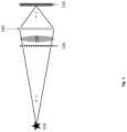
- FIG. 2illustrates an example method for creating, or fabricating, an optical element that performs deconvolution, such as corrective mask 140 of the example of FIG. 1 .
- the example method of FIG. 2may begin at step 210 , which includes propagating, for each of one or more wavelengths ⁇ i , a point source field from an object plane to a corrective mask plane to determine a source field S i .
- step 210includes propagating, for each of one or more wavelengths ⁇ i , a point source field from an object plane to a corrective mask plane to determine a source field S i .
- point source 110lies in an object plane
- the corrective mask planeis the plane in which corrective mask 140 lies.
- This disclosurecontemplates that any suitable number of wavelengths ⁇ i may be used to generate corresponding source fields S i .
- a set of wavelengths across the visible spectrummay be chosen, each wavelength corresponding to a source field S i .
- the method of FIG. 2includes propagating, for each of the one or more wavelengths ⁇ i , the point source field S i from an image plane to the corrective mask plane to determine an image field I i .
- the image planecorresponds to the plane in which sensor 150 is disposed.
- the method of FIG. 2includes determining, for each of the one or more wavelengths ⁇ i , a phase modulation field ⁇ i based on the source field S i and the image field I i .
- each phase modulation field ⁇ imay be equal to
- the method of FIG. 2includes determining a multi-wavelength phase modulation field ⁇ based on combining the phase modulation field for each of the one or more wavelengths ⁇ i .
- the combination of each ⁇ i into the multi-wavelength phase modulation field ⁇may be accomplished using any suitable techniques, such as for example using superposition (complex addition), random sampling, etc.
- Particular embodimentsmay repeat one or more steps of the method of FIG. 2 , where appropriate.
- this disclosuredescribes and illustrates particular steps of the method of FIG. 2 as occurring in a particular order, this disclosure contemplates any suitable steps of the method of FIG. 2 occurring in any suitable order.
- this disclosurecontemplates that some or all of the computing operations described herein, including certain steps of the example method illustrated in FIG. 2 such as steps 230 and 240 , may be performed by circuitry of a computing device described herein, by a processor coupled to non-transitory computer readable storage media, or any suitable combination thereof.
- the multi-wavelength phase modulation field ⁇can be used to design and fabricate a physical corrective optical element, which in particular embodiments may occur after simulation studies are used to test and validate ⁇ .
- a physical corrective optical element that deblurs distortion caused by, e.g., the layers of a device's displaycan be physically generated from the multi-wavelength phase modulation field ⁇ by any of a variety of different fabrication methods known in the field, including, for example binary amplitude masks, phase masks, kinoforms, freeform holographic optical elements, metalenses, etc.
- the optical elementcan be disposed in a device at the location of the corrective mask plane described above.
- the devicecan then perform image deconvolution using the fabricated optical element, without having to deconvolve the images computationally.
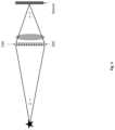
- FIG. 1illustrates an example in which the corrective optical element (correction mask 140 ) is disposed between a display structure (mask 120 ) and an image sensor 150 .
- FIG. 3illustrates another example where the corrective mask 340 is combined (i.e., co-located) with the display mask 320 to form a combined mask.
- a corrective maskmay be placed on the bottom of the display layers of a device.
- a depth sensormay sense electromagnetic waves in a spectrum that includes UV radiation or infrared radiation, or both, and an optical element may be fabricated for the depth sensor by, for example, including wavelengths in those spectrums in steps 210 and 220 of the example method of FIG. 2 .
- FIG. 4illustrates an example optical response of a system using a corrective optical element as described herein.
- FIG. 4illustrates an example display structure mask 410 , with the dark regions indicting non-transparent features of the display mask and the white regions indicating transparent (or partially transparent) regions.
- image 420illustrates the blurring that display structure 410 introduces.
- FIG. 4also illustrates an example of a corrective phase mask 440 , where phase modulation is partly represented by the intensity of the greyscale shown.
- a physical optical elementcan be fabricated from phase mask 440 and introduced to correct the blurring shown in image 420 .
- physical mask 450illustrates an example where a binarized phase mask based on physical mask 440 is combined with the physical structure of display mask 430 .
- the PSF of display mask 450is shown in image 460 , which illustrates deblurring of a point source relative to image 420 for display mask 410 .
- FIG. 5illustrates an example computer system 500 .
- one or more computer systems 500perform one or more steps of one or more methods described or illustrated herein.
- one or more computer systems 500provide functionality described or illustrated herein.
- software running on one or more computer systems 500performs one or more steps of one or more methods described or illustrated herein or provides functionality described or illustrated herein.
- Particular embodimentsinclude one or more portions of one or more computer systems 500 .
- reference to a computer systemmay encompass a computing device, and vice versa, where appropriate.
- reference to a computer systemmay encompass one or more computer systems, where appropriate.
- computer system 500may be an embedded computer system, a system-on-chip (SOC), a single-board computer system (SBC) (such as, for example, a computer-on-module (COM) or system-on-module (SOM)), a desktop computer system, a laptop or notebook computer system, an interactive kiosk, a mainframe, a mesh of computer systems, a mobile telephone, a personal digital assistant (PDA), a server, a tablet computer system, or a combination of two or more of these.
- SOCsystem-on-chip
- SBCsingle-board computer system
- COMcomputer-on-module
- SOMsystem-on-module
- desktop computer systemsuch as, for example, a computer-on-module (COM) or system-on-module (SOM)
- laptop or notebook computer systemsuch as, for example, a computer-on-module (COM) or system-on-module (SOM)
- desktop computer systemsuch as, for example, a computer-on-module (COM
- computer system 500may include one or more computer systems 500 ; be unitary or distributed; span multiple locations; span multiple machines; span multiple data centers; or reside in a cloud, which may include one or more cloud components in one or more networks.
- one or more computer systems 500may perform without substantial spatial or temporal limitation one or more steps of one or more methods described or illustrated herein.
- one or more computer systems 500may perform in real time or in batch mode one or more steps of one or more methods described or illustrated herein.
- One or more computer systems 500may perform at different times or at different locations one or more steps of one or more methods described or illustrated herein, where appropriate.
- computer system 500includes a processor 502 , memory 504 , storage 506 , an input/output (I/O) interface 508 , a communication interface 510 , and a bus 512 .
- I/Oinput/output
- this disclosuredescribes and illustrates a particular computer system having a particular number of particular components in a particular arrangement, this disclosure contemplates any suitable computer system having any suitable number of any suitable components in any suitable arrangement.
- processor 502includes hardware for executing instructions, such as those making up a computer program.
- processor 502may retrieve (or fetch) the instructions from an internal register, an internal cache, memory 504 , or storage 506 ; decode and execute them; and then write one or more results to an internal register, an internal cache, memory 504 , or storage 506 .
- processor 502may include one or more internal caches for data, instructions, or addresses. This disclosure contemplates processor 502 including any suitable number of any suitable internal caches, where appropriate.
- processor 502may include one or more instruction caches, one or more data caches, and one or more translation lookaside buffers (TLBs). Instructions in the instruction caches may be copies of instructions in memory 504 or storage 506 , and the instruction caches may speed up retrieval of those instructions by processor 502 . Data in the data caches may be copies of data in memory 504 or storage 506 for instructions executing at processor 502 to operate on; the results of previous instructions executed at processor 502 for access by subsequent instructions executing at processor 502 or for writing to memory 504 or storage 506 ; or other suitable data. The data caches may speed up read or write operations by processor 502 . The TLBs may speed up virtual-address translation for processor 502 .
- TLBstranslation lookaside buffers
- processor 502may include one or more internal registers for data, instructions, or addresses. This disclosure contemplates processor 502 including any suitable number of any suitable internal registers, where appropriate. Where appropriate, processor 502 may include one or more arithmetic logic units (ALUs); be a multi-core processor; or include one or more processors 502 . Although this disclosure describes and illustrates a particular processor, this disclosure contemplates any suitable processor.
- ALUsarithmetic logic units
- memory 504includes main memory for storing instructions for processor 502 to execute or data for processor 502 to operate on.
- computer system 500may load instructions from storage 506 or another source (such as, for example, another computer system 500 ) to memory 504 .
- Processor 502may then load the instructions from memory 504 to an internal register or internal cache.
- processor 502may retrieve the instructions from the internal register or internal cache and decode them.
- processor 502may write one or more results (which may be intermediate or final results) to the internal register or internal cache.
- Processor 502may then write one or more of those results to memory 504 .
- processor 502executes only instructions in one or more internal registers or internal caches or in memory 504 (as opposed to storage 506 or elsewhere) and operates only on data in one or more internal registers or internal caches or in memory 504 (as opposed to storage 506 or elsewhere).
- One or more memory buses(which may each include an address bus and a data bus) may couple processor 502 to memory 504 .
- Bus 512may include one or more memory buses, as described below.
- one or more memory management unitsreside between processor 502 and memory 504 and facilitate accesses to memory 504 requested by processor 502 .
- memory 504includes random access memory (RAM).
- This RAMmay be volatile memory, where appropriate Where appropriate, this RAM may be dynamic RAM (DRAM) or static RAM (SRAM). Moreover, where appropriate, this RAM may be single-ported or multi-ported RAM. This disclosure contemplates any suitable RAM.
- Memory 504may include one or more memories 504 , where appropriate. Although this disclosure describes and illustrates particular memory, this disclosure contemplates any suitable memory.
- storage 506includes mass storage for data or instructions.
- storage 506may include a hard disk drive (HDD), a floppy disk drive, flash memory, an optical disc, a magneto-optical disc, magnetic tape, or a Universal Serial Bus (USB) drive or a combination of two or more of these.
- Storage 506may include removable or non-removable (or fixed) media, where appropriate.
- Storage 506may be internal or external to computer system 500 , where appropriate.
- storage 506is non-volatile, solid-state memory.
- storage 506includes read-only memory (ROM).
- this ROMmay be mask-programmed ROM, programmable ROM (PROM), erasable PROM (EPROM), electrically erasable PROM (EEPROM), electrically alterable ROM (EAROM), or flash memory or a combination of two or more of these.
- This disclosurecontemplates mass storage 506 taking any suitable physical form.
- Storage 506may include one or more storage control units facilitating communication between processor 502 and storage 506 , where appropriate.
- storage 506may include one or more storages 506 .
- this disclosuredescribes and illustrates particular storage, this disclosure contemplates any suitable storage.
- I/O interface 508includes hardware, software, or both, providing one or more interfaces for communication between computer system 500 and one or more I/O devices.
- Computer system 500may include one or more of these I/O devices, where appropriate.
- One or more of these I/O devicesmay enable communication between a person and computer system 500 .
- an I/O devicemay include a keyboard, keypad, microphone, monitor, mouse, printer, scanner, speaker, still camera, stylus, tablet, touch screen, trackball, video camera, another suitable I/O device or a combination of two or more of these.
- An I/O devicemay include one or more sensors. This disclosure contemplates any suitable I/O devices and any suitable I/O interfaces 508 for them.
- I/O interface 508may include one or more device or software drivers enabling processor 502 to drive one or more of these I/O devices.
- I/O interface 508may include one or more I/O interfaces 508 , where appropriate. Although this disclosure describes and illustrates a particular I/O interface, this disclosure contemplates any suitable I/O interface.
- communication interface 510includes hardware, software, or both providing one or more interfaces for communication (such as, for example, packet-based communication) between computer system 500 and one or more other computer systems 500 or one or more networks.
- communication interface 510may include a network interface controller (NIC) or network adapter for communicating with an Ethernet or other wire-based network or a wireless NIC (WNIC) or wireless adapter for communicating with a wireless network, such as a WI-FI network.
- NICnetwork interface controller
- WNICwireless NIC
- WI-FI networkwireless network
- computer system 500may communicate with an ad hoc network, a personal area network (PAN), a local area network (LAN), a wide area network (WAN), a metropolitan area network (MAN), or one or more portions of the Internet or a combination of two or more of these.
- PANpersonal area network
- LANlocal area network
- WANwide area network
- MANmetropolitan area network
- computer system 500may communicate with a wireless PAN (WPAN) (such as, for example, a BLUETOOTH WPAN), a WI-FI network, a WI-MAX network, a cellular telephone network (such as, for example, a Global System for Mobile Communications (GSM) network), or other suitable wireless network or a combination of two or more of these.
- WPANwireless PAN
- WI-FIwireless personal area network
- WI-MAXwireless personal area network
- WI-MAXwireless personal area network
- cellular telephone networksuch as, for example, a Global System for Mobile Communications (GSM) network
- GSMGlobal System
- bus 512includes hardware, software, or both coupling components of computer system 500 to each other.
- bus 512may include an Accelerated Graphics Port (AGP) or other graphics bus, an Enhanced Industry Standard Architecture (EISA) bus, a front-side bus (FSB), a HYPERTRANSPORT (HT) interconnect, an Industry Standard Architecture (ISA) bus, an INFINIBAND interconnect, a low-pin-count (LPC) bus, a memory bus, a Micro Channel Architecture (MCA) bus, a Peripheral Component Interconnect (PCI) bus, a PCI-Express (PCIe) bus, a serial advanced technology attachment (SATA) bus, a Video Electronics Standards Association local (VLB) bus, or another suitable bus or a combination of two or more of these.
- Bus 512may include one or more buses 512 , where appropriate.
- a computer-readable non-transitory storage medium or mediamay include one or more semiconductor-based or other integrated circuits (ICs) (such, as for example, field-programmable gate arrays (FPGAs) or application-specific ICs (ASICs)), hard disk drives (HDDs), hybrid hard drives (HHDs), optical discs, optical disc drives (ODDs), magneto-optical discs, magneto-optical drives, floppy diskettes, floppy disk drives (FDDs), magnetic tapes, solid-state drives (SSDs), RAM-drives, SECURE DIGITAL cards or drives, any other suitable computer-readable non-transitory storage media, or any suitable combination of two or more of these, where appropriate.
- ICssuch, as for example, field-programmable gate arrays (FPGAs) or application-specific ICs (ASICs)
- HDDshard disk drives
- HHDshybrid hard drives
- ODDsoptical disc drives
- magneto-optical discsmagneto-optical drives
Landscapes
- Physics & Mathematics (AREA)
- General Physics & Mathematics (AREA)
- Engineering & Computer Science (AREA)
- Optics & Photonics (AREA)
- Theoretical Computer Science (AREA)
- Multimedia (AREA)
- Signal Processing (AREA)
- Computing Systems (AREA)
- Image Processing (AREA)
Abstract
Description
Claims (20)
Priority Applications (3)
| Application Number | Priority Date | Filing Date | Title |
|---|---|---|---|
| US17/963,609US12216277B2 (en) | 2021-10-14 | 2022-10-11 | Optical element for deconvolution |
| EP22881419.0AEP4327058A4 (en) | 2021-10-14 | 2022-10-14 | METHOD AND DEVICE FOR OPTICAL UNFOLDING |
| PCT/KR2022/015641WO2023063792A1 (en) | 2021-10-14 | 2022-10-14 | A method and apparatus for optical deconvolution |
Applications Claiming Priority (2)
| Application Number | Priority Date | Filing Date | Title |
|---|---|---|---|
| US202163255819P | 2021-10-14 | 2021-10-14 | |
| US17/963,609US12216277B2 (en) | 2021-10-14 | 2022-10-11 | Optical element for deconvolution |
Publications (2)
| Publication Number | Publication Date |
|---|---|
| US20230119549A1 US20230119549A1 (en) | 2023-04-20 |
| US12216277B2true US12216277B2 (en) | 2025-02-04 |
Family
ID=85982954
Family Applications (1)
| Application Number | Title | Priority Date | Filing Date |
|---|---|---|---|
| US17/963,609Active2042-11-23US12216277B2 (en) | 2021-10-14 | 2022-10-11 | Optical element for deconvolution |
Country Status (3)
| Country | Link |
|---|---|
| US (1) | US12216277B2 (en) |
| EP (1) | EP4327058A4 (en) |
| WO (1) | WO2023063792A1 (en) |
Families Citing this family (1)
| Publication number | Priority date | Publication date | Assignee | Title |
|---|---|---|---|---|
| CN117073840B (en)* | 2023-10-13 | 2023-12-29 | 深圳市中达瑞和科技有限公司 | Multispectral imaging method, multispectral imaging system and multispectral imaging related equipment based on optimal computational imaging |
Citations (116)
| Publication number | Priority date | Publication date | Assignee | Title |
|---|---|---|---|---|
| US3971065A (en) | 1975-03-05 | 1976-07-20 | Eastman Kodak Company | Color imaging array |
| US6454414B1 (en) | 2000-05-24 | 2002-09-24 | Chi Mei Optoelectronics Corporation | Device for image output and input |
| US20030002746A1 (en) | 2000-09-28 | 2003-01-02 | Yosuke Kusaka | Image creating device and image creating method |
| US20060103951A1 (en) | 2002-03-17 | 2006-05-18 | Bell Gareth P | Method to control point spread function of an image |
| US7053613B2 (en) | 2004-06-03 | 2006-05-30 | Fa-Hsuan Lin | Method for parallel image reconstruction using automatic regularization |
| US20060256226A1 (en) | 2003-01-16 | 2006-11-16 | D-Blur Technologies Ltd. | Camera with image enhancement functions |
| US20080013850A1 (en) | 2006-07-14 | 2008-01-17 | Junzou Sakurai | Image processing apparatus and image restoration method and program |
| US20080068660A1 (en) | 2006-09-18 | 2008-03-20 | Xerox Corporation | Sharpening a halftoned image |
| JP2008070566A (en) | 2006-09-13 | 2008-03-27 | Matsushita Electric Ind Co Ltd | Camera system, camera body, interchangeable lens unit, and image blur correction method |
| US20080165261A1 (en) | 2007-01-09 | 2008-07-10 | Yuji Kamo | Imaging apparatus adapted to implement electrical image restoration processing |
| US20080166115A1 (en) | 2007-01-05 | 2008-07-10 | David Sachs | Method and apparatus for producing a sharp image from a handheld device containing a gyroscope |
| US20080218597A1 (en) | 2007-03-06 | 2008-09-11 | Sony Corporation | Solid-state imaging device and imaging apparatus |
| US20080292135A1 (en) | 2005-11-01 | 2008-11-27 | Carl Zeiss Imaging Solutions Gmbh | Method and Device For Reconstructing Images |
| CN101414094A (en) | 2007-10-15 | 2009-04-22 | 佳能株式会社 | Optical apparatus including image blur correction device |
| US20090147111A1 (en) | 2005-11-10 | 2009-06-11 | D-Blur Technologies Ltd. | Image enhancement in the mosaic domain |
| US20090263043A1 (en) | 2005-10-14 | 2009-10-22 | Consejo Superior De Investigaciones Cientificas | Blind deconvolution and super-resolution method for sequences and sets of images and applications thereof |
| US20100073518A1 (en) | 2008-09-24 | 2010-03-25 | Michael Victor Yeh | Using distance/proximity information when applying a point spread function in a portable media device |
| WO2010081229A1 (en) | 2009-01-19 | 2010-07-22 | The University Of British Columbia | Multiplexed imaging |
| US20100188528A1 (en) | 2009-01-28 | 2010-07-29 | Kabushiki Kaisha Toshiba | Image recording device, manufacturing apparatus of image recording device, and manufacturing method of image recording device |
| US20110019056A1 (en) | 2009-07-26 | 2011-01-27 | Massachusetts Institute Of Technology | Bi-Directional Screen |
| US20110075257A1 (en) | 2009-09-14 | 2011-03-31 | The Arizona Board Of Regents On Behalf Of The University Of Arizona | 3-Dimensional electro-optical see-through displays |
| US20110158541A1 (en) | 2009-12-25 | 2011-06-30 | Shinji Watanabe | Image processing device, image processing method and program |
| US20110221888A1 (en) | 2010-03-15 | 2011-09-15 | Samsung Electronics Co., Ltd. | Apparatus, method and computer-readable medium imaging through at least one aperture of each pixel of display panel |
| US20110285680A1 (en) | 2010-05-19 | 2011-11-24 | Sony Corporation | Image display device, electronic apparatus, image display system, method of acquiring method, and program |
| US20120057072A1 (en) | 2010-09-06 | 2012-03-08 | Canon Kabushiki Kaisha | Focus adjustment apparatus and image capturing apparatus |
| US20120162490A1 (en) | 2010-12-23 | 2012-06-28 | Samsung Mobile Display Co., Ltd. | Image Capturing Apparatus and Photographing Method Using the Same |
| US20120327277A1 (en) | 2009-07-17 | 2012-12-27 | Searete Llc | Color filters and demosaicing techniques for digital imaging |
| US20130010077A1 (en) | 2011-01-27 | 2013-01-10 | Khang Nguyen | Three-dimensional image capturing apparatus and three-dimensional image capturing method |
| US8433152B2 (en) | 2009-12-18 | 2013-04-30 | Sony Corporation | Information processing apparatus, information processing method, and program |
| US20130147778A1 (en) | 2010-08-31 | 2013-06-13 | Dolby Laboratories Licensing Corporation | Ambient Black Level |
| US20130182062A1 (en) | 2012-01-12 | 2013-07-18 | Samsung Electronics Co. Ltd. | Apparatus and method for taking image and conducting video communication |
| US8582911B2 (en) | 2010-03-12 | 2013-11-12 | Samsung Electronics Co., Ltd. | Image restoration device, image restoration method and image restoration system |
| US8587703B2 (en) | 2009-12-01 | 2013-11-19 | Aptina Imaging Corporation | Systems and methods for image restoration |
| US20130308007A1 (en) | 2012-05-18 | 2013-11-21 | Canon Kabushiki Kaisha | Image processing apparatus, image pickup apparatus, image processing method, and image processing program |
| US20130321686A1 (en) | 2012-06-01 | 2013-12-05 | Kar-Han Tan | Display-camera system with switchable diffuser |
| US20130336597A1 (en) | 2011-06-17 | 2013-12-19 | Panasonic Corporation | Image stabilization apparatus, image stabilization method, and document |
| US20140044314A1 (en) | 2012-08-13 | 2014-02-13 | Texas Instruments Incorporated | Dynamic Focus for Computational Imaging |
| US20150049165A1 (en) | 2013-08-16 | 2015-02-19 | Kwonhue CHOI | Apparatus for eye contact video call |
| US20150101411A1 (en) | 2013-10-11 | 2015-04-16 | Seno Medical Instruments, Inc. | Systems and methods for component separation in medical imaging |
| US20150207962A1 (en) | 2013-03-28 | 2015-07-23 | Fujifilm Corporation | Image-processing device, image-capturing device, image-processing method, and recording medium |
| US20150338639A1 (en)* | 2012-02-03 | 2015-11-26 | Citizen Holdings Co., Ltd. | Phase modulation device and laser microscope |
| US9220481B2 (en) | 2011-10-05 | 2015-12-29 | Samsung Electronics Co., Ltd. | Diagnostic image generating apparatus, medical image system, and beamforming method |
| US20160062100A1 (en)* | 2014-08-26 | 2016-03-03 | The Board Of Trustees Of The Leland Stanford Junior University | Light-field microscopy with phase masking |
| US9338354B2 (en) | 2011-10-03 | 2016-05-10 | Nikon Corporation | Motion blur estimation and restoration using light trails |
| US20160180510A1 (en) | 2014-12-23 | 2016-06-23 | Oliver Grau | Method and system of geometric camera self-calibration quality assessment |
| US20160248975A1 (en) | 2015-02-19 | 2016-08-25 | Blackberry Limited | Device with a front facing camera having discrete focus positions |
| US20160277658A1 (en) | 2015-03-16 | 2016-09-22 | Dae Kwan Kim | Image signal processor and devices including the same |
| WO2016154392A1 (en) | 2015-03-24 | 2016-09-29 | University Of Florida Research Foundation, Inc. | Optical privatizing device, system and method of use |
| US20160371821A1 (en) | 2014-03-28 | 2016-12-22 | Fujifilm Corporation | Image processing device, imaging device, image processing method, and program |
| US9582862B2 (en) | 2014-12-30 | 2017-02-28 | Huazhong University Of Science And Technology | Direction-adaptive image deblurring method |
| US20170076430A1 (en) | 2014-05-28 | 2017-03-16 | Huawei Technologies Co., Ltd. | Image Processing Method and Image Processing Apparatus |
| US20170104897A1 (en) | 2015-10-08 | 2017-04-13 | Samsung Electro-Mechanics Co., Ltd. | Camera module, electronic device, and method of operating the same |
| US9654707B2 (en) | 2014-10-21 | 2017-05-16 | Canon Kabushiki Kaisha | Image processing apparatus, image capturing apparatus, image processing method and storage medium storing image processing program |
| WO2017117152A1 (en) | 2016-01-01 | 2017-07-06 | Kla-Tencor Corporation | Systems and methods for defect detection using image reconstruction |
| US20170212613A1 (en) | 2016-01-21 | 2017-07-27 | Samsung Electronics Co., Ltd | Disposition structure of sensor of electronic device |
| US20170316552A1 (en) | 2016-04-27 | 2017-11-02 | Ramot At Tel-Aviv University Ltd. | Blind image deblurring via progressive removal of blur residual |
| US20180038768A1 (en) | 2015-03-05 | 2018-02-08 | Eyenetra, Inc. | Methods and Apparatus for Small Aperture Lensometer |
| US20180052050A1 (en) | 2015-03-24 | 2018-02-22 | University Of Utah Research Foundation | Imaging device with image dispersing to create a spatially coded image |
| US9911208B2 (en) | 2016-04-11 | 2018-03-06 | Toshiba Medical Systems Corporation | Apparatus and method of iterative image reconstruction using regularization-parameter control |
| US9916656B2 (en) | 2015-08-26 | 2018-03-13 | Drtech Corp | Method for processing radiographic image and radiography system |
| US9947901B2 (en) | 2013-01-02 | 2018-04-17 | Apple Inc. | Electronic devices with light sensors and displays |
| US20180116500A1 (en) | 2015-06-23 | 2018-05-03 | Essil Or International (Compagnie General D'optique) | Optometry measuring scale |
| US20180129061A1 (en) | 2015-07-29 | 2018-05-10 | Omron Corporation | Optical device |
| US20180198980A1 (en) | 2017-01-06 | 2018-07-12 | Intel Corporation | Integrated Image Sensor and Display Pixel |
| US10032254B2 (en) | 2010-09-28 | 2018-07-24 | MAX-PLANCK-Gesellschaft zur Förderung der Wissenschaften e.V. | Method and device for recovering a digital image from a sequence of observed digital images |
| US20180211420A1 (en) | 2015-07-17 | 2018-07-26 | Samsung Electronics Co., Ltd. | Tomographic device and tomographic image processing method according to same |
| US10062153B2 (en) | 2015-05-19 | 2018-08-28 | Canon Kabushiki Kaisha | Image processing apparatus, image pickup apparatus, image processing method, and storage medium |
| US10083335B2 (en) | 2014-06-20 | 2018-09-25 | Vkansee Technology Company Ltd. | Image acquisition apparatus, terminal device, liquid crystal terminal device and image acquisition method |
| US10151933B2 (en) | 2013-12-20 | 2018-12-11 | Sony Corporation | Apparatus and optical system including an optical element |
| US10178381B2 (en) | 2015-07-14 | 2019-01-08 | Microsoft Technology Licensing, Llc | Depth-spatial frequency-response assessment |
| US10191577B2 (en) | 2016-02-16 | 2019-01-29 | Samsung Electronics Co., Ltd. | Electronic device |
| US10217190B2 (en) | 2016-12-27 | 2019-02-26 | Kla-Tencor Corporation | System and method for reconstructing high-resolution point spread functions from low-resolution inspection images |
| JP2019068378A (en) | 2017-10-05 | 2019-04-25 | 株式会社コンフォートビジョン研究所 | High resolution imaging device |
| US20190213717A1 (en) | 2018-01-05 | 2019-07-11 | Canon Kabushiki Kaisha | Image processing method, imaging apparatus using the same, image processing apparatus, storage medium, and lens apparatus |
| US20190212544A1 (en) | 2016-09-16 | 2019-07-11 | Fraunhofer-Gesellschaft Zurfoerderung Der Angewandten Forschung E.V. | Optical arrangement for generating light field distributions and method for operating an optical arrangement |
| US20190327417A1 (en) | 2015-08-20 | 2019-10-24 | Kabushiki Kaisha Toshiba | Image processing apparatus and image capturing apparatus |
| US20190355101A1 (en) | 2017-01-12 | 2019-11-21 | Intel Corporation | Image refocusing |
| JP6652052B2 (en) | 2014-06-03 | 2020-02-19 | ソニー株式会社 | Image processing apparatus and image processing method |
| US10595724B2 (en) | 2017-08-04 | 2020-03-24 | Ho Wa LAI | Adaptor for an image capture device for fundus photography |
| US10642059B2 (en) | 2014-08-14 | 2020-05-05 | Yakov Soskind | Optical field transformation methods and systems |
| US10656437B2 (en) | 2011-12-21 | 2020-05-19 | Brien Holden Vision Institute Limited | Optical lens with halo reduction |
| US20200159102A1 (en)* | 2017-08-07 | 2020-05-21 | Sony Corporation | Phase modulator, lighting system, and projector |
| US20200169725A1 (en) | 2017-05-18 | 2020-05-28 | Arizona Board Regents On Behalf Of The University Of Arizona | Multilayer high-dynamic-range head-mounted display |
| US20200166807A1 (en) | 2018-11-28 | 2020-05-28 | Kabushiki Kaisha Toshiba | Image processing device, image capturing device, and image processing method |
| US20200209604A1 (en) | 2017-08-04 | 2020-07-02 | Nanjing University Of Science And Technology | Programmable annular led illumination-based high efficiency quantitative phase microscopy imaging method |
| US20200321561A1 (en) | 2019-04-03 | 2020-10-08 | Samsung Display Co., Ltd. | Display apparatus and method of manufacturing the same |
| US20200389575A1 (en) | 2019-06-05 | 2020-12-10 | Synaptics Incorporated | Under-display image sensor |
| US20200394964A1 (en) | 2019-06-17 | 2020-12-17 | Samsung Display Co., Ltd. | Display device |
| CN112202991A (en) | 2020-09-17 | 2021-01-08 | 欧菲微电子技术有限公司 | Camera module, electronic equipment, optical element and preparation method of camera module |
| US20210029336A1 (en) | 2019-07-26 | 2021-01-28 | Samsung Electronics Company, Ltd. | Processing images captured by a camera behind a display |
| US20210136335A1 (en)* | 2017-08-07 | 2021-05-06 | Sony Corporation | Phase modulator, lighting system, and projector |
| US11003088B2 (en) | 2006-01-30 | 2021-05-11 | Carl Zeiss Smt Gmbh | Method and device for the correction of imaging defects |
| US20210152735A1 (en) | 2019-11-14 | 2021-05-20 | Microsoft Technology Licensing, Llc | Image restoration for through-display imaging |
| US11038143B2 (en) | 2018-12-06 | 2021-06-15 | Samsung Display Co., Ltd. | Display device and electronic device having the same |
| WO2021122471A1 (en) | 2019-12-17 | 2021-06-24 | Testa Ilaria | Imaging system |
| US20210193756A1 (en) | 2019-12-18 | 2021-06-24 | Lg Display Co., Ltd. | Display device |
| CN113053253A (en) | 2020-10-19 | 2021-06-29 | 上海鲲游科技有限公司 | Optical system under screen, phase compensation element and method thereof, and electronic device |
| US20210199952A1 (en) | 2018-09-26 | 2021-07-01 | Guangdong Oppo Mobile Telecommunications Corp., Ltd. | Method and Device for Recovering Image Passing Through Display |
| CN113067961A (en) | 2020-10-19 | 2021-07-02 | 上海鲲游科技有限公司 | Under-screen camera imaging system, phase compensation element and manufacturing method thereof |
| US20210210533A1 (en) | 2018-09-26 | 2021-07-08 | Guangdong Oppo Mobile Telecommunications Corp., Ltd. | Imaging Device and Electric Device |
| US11073712B2 (en) | 2018-04-10 | 2021-07-27 | Apple Inc. | Electronic device display for through-display imaging |
| US20210233976A1 (en) | 2020-01-23 | 2021-07-29 | Samsung Display Co., Ltd. | Display device |
| CN108335268B (en) | 2018-01-05 | 2021-09-07 | 广西师范大学 | A Color Image Deblurring Method Based on Blind Deconvolution |
| US20210302316A1 (en) | 2020-03-27 | 2021-09-30 | Leica Microsystems Cms Gmbh | Method and device for estimating a sted resolution |
| WO2022005157A1 (en) | 2020-07-02 | 2022-01-06 | Samsung Electronics Co., Ltd. | Electronic device and controlling method of electronic device |
| KR20220014764A (en) | 2020-07-29 | 2022-02-07 | 삼성전자주식회사 | Electronic device and method for generating training data of artificial intelligence learning model thereof |
| US20220067889A1 (en) | 2020-08-31 | 2022-03-03 | Samsung Electronics Co., Ltd. | Image enhancement method, image enhancement apparatus, and method and apparatus for training image enhancement apparatus |
| US11272106B1 (en) | 2020-08-31 | 2022-03-08 | Samsung Electronics Co., Ltd. | Method and apparatus for image acquisition including image sensor |
| US20220086309A1 (en) | 2019-06-05 | 2022-03-17 | Samsung Electronics Co., Ltd. | Depth map determination method and electronic device to which same method is applied |
| CN114331886A (en) | 2021-12-23 | 2022-04-12 | 西安工业大学 | Image deblurring method based on depth features |
| US20220138924A1 (en) | 2020-10-30 | 2022-05-05 | Samsung Electronics Co., Ltd. | Image restoration method and apparatus |
| CN110675347B (en) | 2019-09-30 | 2022-05-06 | 北京工业大学 | Image blind restoration method based on group sparse representation |
| US20220261966A1 (en) | 2021-02-16 | 2022-08-18 | Samsung Electronics Company, Ltd. | Multiple point spread function based image reconstruction for a camera behind a display |
| US20220277426A1 (en) | 2021-02-26 | 2022-09-01 | Samsung Electronics Company, Ltd. | Self-regularizing inverse filter for image deblurring |
| US20220292637A1 (en) | 2020-06-16 | 2022-09-15 | Mayo Foundation For Medical Education And Research | Methods for High Spatial and Temporal Resolution Ultrasound Imaging of Microvessels |
| US20230341264A1 (en)* | 2020-02-03 | 2023-10-26 | Viavi Solutions Inc. | Optical sensor device |
- 2022
- 2022-10-11USUS17/963,609patent/US12216277B2/enactiveActive
- 2022-10-14EPEP22881419.0Apatent/EP4327058A4/enactivePending
- 2022-10-14WOPCT/KR2022/015641patent/WO2023063792A1/ennot_activeCeased
Patent Citations (123)
| Publication number | Priority date | Publication date | Assignee | Title |
|---|---|---|---|---|
| US3971065A (en) | 1975-03-05 | 1976-07-20 | Eastman Kodak Company | Color imaging array |
| US6454414B1 (en) | 2000-05-24 | 2002-09-24 | Chi Mei Optoelectronics Corporation | Device for image output and input |
| US20030002746A1 (en) | 2000-09-28 | 2003-01-02 | Yosuke Kusaka | Image creating device and image creating method |
| US20060103951A1 (en) | 2002-03-17 | 2006-05-18 | Bell Gareth P | Method to control point spread function of an image |
| US20060256226A1 (en) | 2003-01-16 | 2006-11-16 | D-Blur Technologies Ltd. | Camera with image enhancement functions |
| US7053613B2 (en) | 2004-06-03 | 2006-05-30 | Fa-Hsuan Lin | Method for parallel image reconstruction using automatic regularization |
| US20090263043A1 (en) | 2005-10-14 | 2009-10-22 | Consejo Superior De Investigaciones Cientificas | Blind deconvolution and super-resolution method for sequences and sets of images and applications thereof |
| US20080292135A1 (en) | 2005-11-01 | 2008-11-27 | Carl Zeiss Imaging Solutions Gmbh | Method and Device For Reconstructing Images |
| US8041142B2 (en) | 2005-11-01 | 2011-10-18 | Carl Zeiss Imaging Solutions Gmbh | Method and device for reconstructing images |
| US20090147111A1 (en) | 2005-11-10 | 2009-06-11 | D-Blur Technologies Ltd. | Image enhancement in the mosaic domain |
| US11003088B2 (en) | 2006-01-30 | 2021-05-11 | Carl Zeiss Smt Gmbh | Method and device for the correction of imaging defects |
| US20080013850A1 (en) | 2006-07-14 | 2008-01-17 | Junzou Sakurai | Image processing apparatus and image restoration method and program |
| JP2008070566A (en) | 2006-09-13 | 2008-03-27 | Matsushita Electric Ind Co Ltd | Camera system, camera body, interchangeable lens unit, and image blur correction method |
| US20080068660A1 (en) | 2006-09-18 | 2008-03-20 | Xerox Corporation | Sharpening a halftoned image |
| US20080166115A1 (en) | 2007-01-05 | 2008-07-10 | David Sachs | Method and apparatus for producing a sharp image from a handheld device containing a gyroscope |
| US20080165261A1 (en) | 2007-01-09 | 2008-07-10 | Yuji Kamo | Imaging apparatus adapted to implement electrical image restoration processing |
| US20080218597A1 (en) | 2007-03-06 | 2008-09-11 | Sony Corporation | Solid-state imaging device and imaging apparatus |
| CN101414094A (en) | 2007-10-15 | 2009-04-22 | 佳能株式会社 | Optical apparatus including image blur correction device |
| US20100073518A1 (en) | 2008-09-24 | 2010-03-25 | Michael Victor Yeh | Using distance/proximity information when applying a point spread function in a portable media device |
| WO2010081229A1 (en) | 2009-01-19 | 2010-07-22 | The University Of British Columbia | Multiplexed imaging |
| US20100188528A1 (en) | 2009-01-28 | 2010-07-29 | Kabushiki Kaisha Toshiba | Image recording device, manufacturing apparatus of image recording device, and manufacturing method of image recording device |
| US20120327277A1 (en) | 2009-07-17 | 2012-12-27 | Searete Llc | Color filters and demosaicing techniques for digital imaging |
| US20110019056A1 (en) | 2009-07-26 | 2011-01-27 | Massachusetts Institute Of Technology | Bi-Directional Screen |
| US20110075257A1 (en) | 2009-09-14 | 2011-03-31 | The Arizona Board Of Regents On Behalf Of The University Of Arizona | 3-Dimensional electro-optical see-through displays |
| US8587703B2 (en) | 2009-12-01 | 2013-11-19 | Aptina Imaging Corporation | Systems and methods for image restoration |
| US8433152B2 (en) | 2009-12-18 | 2013-04-30 | Sony Corporation | Information processing apparatus, information processing method, and program |
| US20110158541A1 (en) | 2009-12-25 | 2011-06-30 | Shinji Watanabe | Image processing device, image processing method and program |
| US8582911B2 (en) | 2010-03-12 | 2013-11-12 | Samsung Electronics Co., Ltd. | Image restoration device, image restoration method and image restoration system |
| US20110221888A1 (en) | 2010-03-15 | 2011-09-15 | Samsung Electronics Co., Ltd. | Apparatus, method and computer-readable medium imaging through at least one aperture of each pixel of display panel |
| US20110285680A1 (en) | 2010-05-19 | 2011-11-24 | Sony Corporation | Image display device, electronic apparatus, image display system, method of acquiring method, and program |
| US20130147778A1 (en) | 2010-08-31 | 2013-06-13 | Dolby Laboratories Licensing Corporation | Ambient Black Level |
| US20120057072A1 (en) | 2010-09-06 | 2012-03-08 | Canon Kabushiki Kaisha | Focus adjustment apparatus and image capturing apparatus |
| US10032254B2 (en) | 2010-09-28 | 2018-07-24 | MAX-PLANCK-Gesellschaft zur Förderung der Wissenschaften e.V. | Method and device for recovering a digital image from a sequence of observed digital images |
| US20120162490A1 (en) | 2010-12-23 | 2012-06-28 | Samsung Mobile Display Co., Ltd. | Image Capturing Apparatus and Photographing Method Using the Same |
| US20130010077A1 (en) | 2011-01-27 | 2013-01-10 | Khang Nguyen | Three-dimensional image capturing apparatus and three-dimensional image capturing method |
| US20130336597A1 (en) | 2011-06-17 | 2013-12-19 | Panasonic Corporation | Image stabilization apparatus, image stabilization method, and document |
| US9338354B2 (en) | 2011-10-03 | 2016-05-10 | Nikon Corporation | Motion blur estimation and restoration using light trails |
| KR101894391B1 (en) | 2011-10-05 | 2018-09-04 | 삼성전자주식회사 | Apparatus for generating diagnosis image, medical imaging system, and method for beamforming |
| US9220481B2 (en) | 2011-10-05 | 2015-12-29 | Samsung Electronics Co., Ltd. | Diagnostic image generating apparatus, medical image system, and beamforming method |
| US10656437B2 (en) | 2011-12-21 | 2020-05-19 | Brien Holden Vision Institute Limited | Optical lens with halo reduction |
| US20130182062A1 (en) | 2012-01-12 | 2013-07-18 | Samsung Electronics Co. Ltd. | Apparatus and method for taking image and conducting video communication |
| US20150338639A1 (en)* | 2012-02-03 | 2015-11-26 | Citizen Holdings Co., Ltd. | Phase modulation device and laser microscope |
| US20130308007A1 (en) | 2012-05-18 | 2013-11-21 | Canon Kabushiki Kaisha | Image processing apparatus, image pickup apparatus, image processing method, and image processing program |
| US20130321686A1 (en) | 2012-06-01 | 2013-12-05 | Kar-Han Tan | Display-camera system with switchable diffuser |
| US20140044314A1 (en) | 2012-08-13 | 2014-02-13 | Texas Instruments Incorporated | Dynamic Focus for Computational Imaging |
| US9947901B2 (en) | 2013-01-02 | 2018-04-17 | Apple Inc. | Electronic devices with light sensors and displays |
| US20150207962A1 (en) | 2013-03-28 | 2015-07-23 | Fujifilm Corporation | Image-processing device, image-capturing device, image-processing method, and recording medium |
| US20150049165A1 (en) | 2013-08-16 | 2015-02-19 | Kwonhue CHOI | Apparatus for eye contact video call |
| US20150101411A1 (en) | 2013-10-11 | 2015-04-16 | Seno Medical Instruments, Inc. | Systems and methods for component separation in medical imaging |
| US10151933B2 (en) | 2013-12-20 | 2018-12-11 | Sony Corporation | Apparatus and optical system including an optical element |
| US20160371821A1 (en) | 2014-03-28 | 2016-12-22 | Fujifilm Corporation | Image processing device, imaging device, image processing method, and program |
| US20170076430A1 (en) | 2014-05-28 | 2017-03-16 | Huawei Technologies Co., Ltd. | Image Processing Method and Image Processing Apparatus |
| JP6652052B2 (en) | 2014-06-03 | 2020-02-19 | ソニー株式会社 | Image processing apparatus and image processing method |
| US10083335B2 (en) | 2014-06-20 | 2018-09-25 | Vkansee Technology Company Ltd. | Image acquisition apparatus, terminal device, liquid crystal terminal device and image acquisition method |
| US10642059B2 (en) | 2014-08-14 | 2020-05-05 | Yakov Soskind | Optical field transformation methods and systems |
| US20160062100A1 (en)* | 2014-08-26 | 2016-03-03 | The Board Of Trustees Of The Leland Stanford Junior University | Light-field microscopy with phase masking |
| US9654707B2 (en) | 2014-10-21 | 2017-05-16 | Canon Kabushiki Kaisha | Image processing apparatus, image capturing apparatus, image processing method and storage medium storing image processing program |
| US20160180510A1 (en) | 2014-12-23 | 2016-06-23 | Oliver Grau | Method and system of geometric camera self-calibration quality assessment |
| US9582862B2 (en) | 2014-12-30 | 2017-02-28 | Huazhong University Of Science And Technology | Direction-adaptive image deblurring method |
| US20160248975A1 (en) | 2015-02-19 | 2016-08-25 | Blackberry Limited | Device with a front facing camera having discrete focus positions |
| US20180038768A1 (en) | 2015-03-05 | 2018-02-08 | Eyenetra, Inc. | Methods and Apparatus for Small Aperture Lensometer |
| US9948849B2 (en) | 2015-03-16 | 2018-04-17 | Samsung Electronics Co., Ltd. | Image signal processor and devices including the same |
| US20160277658A1 (en) | 2015-03-16 | 2016-09-22 | Dae Kwan Kim | Image signal processor and devices including the same |
| US20180052050A1 (en) | 2015-03-24 | 2018-02-22 | University Of Utah Research Foundation | Imaging device with image dispersing to create a spatially coded image |
| WO2016154392A1 (en) | 2015-03-24 | 2016-09-29 | University Of Florida Research Foundation, Inc. | Optical privatizing device, system and method of use |
| US10062153B2 (en) | 2015-05-19 | 2018-08-28 | Canon Kabushiki Kaisha | Image processing apparatus, image pickup apparatus, image processing method, and storage medium |
| US20180116500A1 (en) | 2015-06-23 | 2018-05-03 | Essil Or International (Compagnie General D'optique) | Optometry measuring scale |
| US10178381B2 (en) | 2015-07-14 | 2019-01-08 | Microsoft Technology Licensing, Llc | Depth-spatial frequency-response assessment |
| US20180211420A1 (en) | 2015-07-17 | 2018-07-26 | Samsung Electronics Co., Ltd. | Tomographic device and tomographic image processing method according to same |
| US20180129061A1 (en) | 2015-07-29 | 2018-05-10 | Omron Corporation | Optical device |
| US20190327417A1 (en) | 2015-08-20 | 2019-10-24 | Kabushiki Kaisha Toshiba | Image processing apparatus and image capturing apparatus |
| US9916656B2 (en) | 2015-08-26 | 2018-03-13 | Drtech Corp | Method for processing radiographic image and radiography system |
| US20170104897A1 (en) | 2015-10-08 | 2017-04-13 | Samsung Electro-Mechanics Co., Ltd. | Camera module, electronic device, and method of operating the same |
| WO2017117152A1 (en) | 2016-01-01 | 2017-07-06 | Kla-Tencor Corporation | Systems and methods for defect detection using image reconstruction |
| US10416087B2 (en) | 2016-01-01 | 2019-09-17 | Kla-Tencor Corporation | Systems and methods for defect detection using image reconstruction |
| US20170212613A1 (en) | 2016-01-21 | 2017-07-27 | Samsung Electronics Co., Ltd | Disposition structure of sensor of electronic device |
| US10191577B2 (en) | 2016-02-16 | 2019-01-29 | Samsung Electronics Co., Ltd. | Electronic device |
| US9911208B2 (en) | 2016-04-11 | 2018-03-06 | Toshiba Medical Systems Corporation | Apparatus and method of iterative image reconstruction using regularization-parameter control |
| US20170316552A1 (en) | 2016-04-27 | 2017-11-02 | Ramot At Tel-Aviv University Ltd. | Blind image deblurring via progressive removal of blur residual |
| US20190212544A1 (en) | 2016-09-16 | 2019-07-11 | Fraunhofer-Gesellschaft Zurfoerderung Der Angewandten Forschung E.V. | Optical arrangement for generating light field distributions and method for operating an optical arrangement |
| US10217190B2 (en) | 2016-12-27 | 2019-02-26 | Kla-Tencor Corporation | System and method for reconstructing high-resolution point spread functions from low-resolution inspection images |
| US20180198980A1 (en) | 2017-01-06 | 2018-07-12 | Intel Corporation | Integrated Image Sensor and Display Pixel |
| US20190355101A1 (en) | 2017-01-12 | 2019-11-21 | Intel Corporation | Image refocusing |
| US20200169725A1 (en) | 2017-05-18 | 2020-05-28 | Arizona Board Regents On Behalf Of The University Of Arizona | Multilayer high-dynamic-range head-mounted display |
| US10595724B2 (en) | 2017-08-04 | 2020-03-24 | Ho Wa LAI | Adaptor for an image capture device for fundus photography |
| US20200209604A1 (en) | 2017-08-04 | 2020-07-02 | Nanjing University Of Science And Technology | Programmable annular led illumination-based high efficiency quantitative phase microscopy imaging method |
| US20200159102A1 (en)* | 2017-08-07 | 2020-05-21 | Sony Corporation | Phase modulator, lighting system, and projector |
| US20210136335A1 (en)* | 2017-08-07 | 2021-05-06 | Sony Corporation | Phase modulator, lighting system, and projector |
| JP2019068378A (en) | 2017-10-05 | 2019-04-25 | 株式会社コンフォートビジョン研究所 | High resolution imaging device |
| US20190213717A1 (en) | 2018-01-05 | 2019-07-11 | Canon Kabushiki Kaisha | Image processing method, imaging apparatus using the same, image processing apparatus, storage medium, and lens apparatus |
| CN108335268B (en) | 2018-01-05 | 2021-09-07 | 广西师范大学 | A Color Image Deblurring Method Based on Blind Deconvolution |
| US11073712B2 (en) | 2018-04-10 | 2021-07-27 | Apple Inc. | Electronic device display for through-display imaging |
| US20210210533A1 (en) | 2018-09-26 | 2021-07-08 | Guangdong Oppo Mobile Telecommunications Corp., Ltd. | Imaging Device and Electric Device |
| US20210199952A1 (en) | 2018-09-26 | 2021-07-01 | Guangdong Oppo Mobile Telecommunications Corp., Ltd. | Method and Device for Recovering Image Passing Through Display |
| US20200166807A1 (en) | 2018-11-28 | 2020-05-28 | Kabushiki Kaisha Toshiba | Image processing device, image capturing device, and image processing method |
| US11038143B2 (en) | 2018-12-06 | 2021-06-15 | Samsung Display Co., Ltd. | Display device and electronic device having the same |
| US20200321561A1 (en) | 2019-04-03 | 2020-10-08 | Samsung Display Co., Ltd. | Display apparatus and method of manufacturing the same |
| US20220086309A1 (en) | 2019-06-05 | 2022-03-17 | Samsung Electronics Co., Ltd. | Depth map determination method and electronic device to which same method is applied |
| US20200389575A1 (en) | 2019-06-05 | 2020-12-10 | Synaptics Incorporated | Under-display image sensor |
| US20200394964A1 (en) | 2019-06-17 | 2020-12-17 | Samsung Display Co., Ltd. | Display device |
| US11575865B2 (en) | 2019-07-26 | 2023-02-07 | Samsung Electronics Co., Ltd. | Processing images captured by a camera behind a display |
| US20210029336A1 (en) | 2019-07-26 | 2021-01-28 | Samsung Electronics Company, Ltd. | Processing images captured by a camera behind a display |
| CN110675347B (en) | 2019-09-30 | 2022-05-06 | 北京工业大学 | Image blind restoration method based on group sparse representation |
| US20210152735A1 (en) | 2019-11-14 | 2021-05-20 | Microsoft Technology Licensing, Llc | Image restoration for through-display imaging |
| WO2021122471A1 (en) | 2019-12-17 | 2021-06-24 | Testa Ilaria | Imaging system |
| US20210193756A1 (en) | 2019-12-18 | 2021-06-24 | Lg Display Co., Ltd. | Display device |
| US20210233976A1 (en) | 2020-01-23 | 2021-07-29 | Samsung Display Co., Ltd. | Display device |
| US20230341264A1 (en)* | 2020-02-03 | 2023-10-26 | Viavi Solutions Inc. | Optical sensor device |
| US20210302316A1 (en) | 2020-03-27 | 2021-09-30 | Leica Microsystems Cms Gmbh | Method and device for estimating a sted resolution |
| US20220292637A1 (en) | 2020-06-16 | 2022-09-15 | Mayo Foundation For Medical Education And Research | Methods for High Spatial and Temporal Resolution Ultrasound Imaging of Microvessels |
| WO2022005157A1 (en) | 2020-07-02 | 2022-01-06 | Samsung Electronics Co., Ltd. | Electronic device and controlling method of electronic device |
| KR20220014764A (en) | 2020-07-29 | 2022-02-07 | 삼성전자주식회사 | Electronic device and method for generating training data of artificial intelligence learning model thereof |
| US11272106B1 (en) | 2020-08-31 | 2022-03-08 | Samsung Electronics Co., Ltd. | Method and apparatus for image acquisition including image sensor |
| US11792515B2 (en) | 2020-08-31 | 2023-10-17 | Samsung Electronics Co., Ltd. | Method and apparatus for image acquisition including image sensor |
| US20220067889A1 (en) | 2020-08-31 | 2022-03-03 | Samsung Electronics Co., Ltd. | Image enhancement method, image enhancement apparatus, and method and apparatus for training image enhancement apparatus |
| CN112202991A (en) | 2020-09-17 | 2021-01-08 | 欧菲微电子技术有限公司 | Camera module, electronic equipment, optical element and preparation method of camera module |
| CN113067961A (en) | 2020-10-19 | 2021-07-02 | 上海鲲游科技有限公司 | Under-screen camera imaging system, phase compensation element and manufacturing method thereof |
| CN113053253A (en) | 2020-10-19 | 2021-06-29 | 上海鲲游科技有限公司 | Optical system under screen, phase compensation element and method thereof, and electronic device |
| US20220138924A1 (en) | 2020-10-30 | 2022-05-05 | Samsung Electronics Co., Ltd. | Image restoration method and apparatus |
| US20220261966A1 (en) | 2021-02-16 | 2022-08-18 | Samsung Electronics Company, Ltd. | Multiple point spread function based image reconstruction for a camera behind a display |
| US11721001B2 (en)* | 2021-02-16 | 2023-08-08 | Samsung Electronics Co., Ltd. | Multiple point spread function based image reconstruction for a camera behind a display |
| US20220277426A1 (en) | 2021-02-26 | 2022-09-01 | Samsung Electronics Company, Ltd. | Self-regularizing inverse filter for image deblurring |
| CN114331886A (en) | 2021-12-23 | 2022-04-12 | 西安工业大学 | Image deblurring method based on depth features |
Non-Patent Citations (34)
| Title |
|---|
| Anqi Yang et al., 'Designing Display Pixel Layouts for Under-Panel Cameras', IEEE Transactions on Pattern Analysis and Machine Intelligence, vol. 43, No. 7, pp. 2245-2256, Apr. 27, 2021. |
| Eric Yang, Variable Synthetic Depth of Field with Mobile Stereo Cameras, Computer Science Engineering, https://stanford.edu/class/ee367/sections 3.2, 4.3; 2020, retrieved on Jan. 9, 2024. |
| European Patent Office Extended European Search Report in Application No. 228814190-1207/4327058 PCT/KR2022015641, Sep. 19, 2024. |
| European Search Report in EP 20846484.2, Mar. 14, 2022. |
| Final Office Action in U.S. Appl. No. 17/176,535, Nov. 7, 2022. |
| Heide, Felix, et al., "ProxImaL: Efficient Image Optimization Using Proximal Algorithms," SIGGRAPH 16 Technical paper, Jul. 24-28, 2016, Anaheim, CA. SIGGRAPH '16 Technical Paper, Jul. 24-28, 2016, Anaheim, CA, ISBN: 978-1-4503-4279-Jul. 16, 07 DOI: http://dx.doi.org/10.1145/2897824.2925875, 15 pages. |
| Hong, J., et al., "Three-dimensional display technologies of recent interest: principles, status, and issues [Invited]," (Doc. ID 152226), Applied Optics, vol. 50, No. 34, , Dec. 1, 2011, https://www.researchgate.net/publication/51919272, DOI: 10.1364/A0.50.000H87, 0003-6935/11/340H87, © 2011 Optical Society of America, pp. H87-H115 (30 pages). |
| Image Restoration for Under-Display Camera, Yuqian Zhou et al., CVPR 2021, accessed on Oct. 25, 2022 at https://openaccess.thecvf.com/CVPR2021?day=all. |
| International Search Report and Written Opinion for International App. No. PCT/KR2020/009807, Oct. 26, 2020. |
| International Search Report and Written Opinion for International Application No. PCT/KR2023/007313, Aug. 30, 2023. |
| International Search Report and Written Opinion for International Application No. PCT/KR2023/017304, Feb. 2, 2024. |
| Katkovnik Vladhviir et al: "A novel binary and multilevel phase masks for enhanced depth-of-focus infrared imaging", 2018 52nd Asilomar Conference on Signals, Systems, and Computers, IEEE, Oct. 28, 2018 (Oct. 28, 2018), pp. 386-390, XP033520926, DOI: 10.1109/ACSSC.2018.8645129, Oct. 28, 2018. |
| Lai, Richard, "Oppo's under-screen camera is real and taking photos in Shanghai," https://www.engadget.com/2019-06-26-oppo-under-screen-camera-mwc-shanghai.html, Jun. 26, 2019, 8 pgs. |
| Levin, A. et al., "Image and Depth from a Conventional Camera with a Coded Aperture," ACM Transactions on Graphics, vol. 26, No. 3, Article 70, Publication date Jul. 2007, DOI 10.1145/1239451.123952, http://doi.acm.org/10.1145/1239451.1239521, 9 pgs. |
| Lucy, L. B., "An Iterative Technique for the Rectification of Observed Distributions," The Astronomical Journal, vol. 79, No. 6, Jun. 1974, © American Astronomical Society, provided by the NASA Astrophysics Data System, pp. 745-754 (10 pgs). |
| Non-Final Office Action in U.S. Appl. No. 16/935,946, Apr. 5, 2022. |
| Non-Final Office Action in U.S. Appl. No. 17/176,535, Mar. 7, 2022. |
| Non-Final Office Action in U.S. Appl. No. 17/380,995, Jun. 22, 2022. |
| Notice of Allowance in U.S. Appl. No. 16/935,946, Jul. 6, 2022. |
| Notice of Allowance in U.S. Appl. No. 16/935,946, Sep. 30, 2022. |
| Notice of Allowance in U.S. Appl. No. 17/176,535, Mar. 8, 2023. |
| Notice of Allowance in U.S. Appl. No. 17/380,995, Dec. 21, 2022. |
| PCT Search Report and written decision in PCT/KR2022/001024, May 10, 2022. |
| PCT Search Report and Written Decision in PCT/KR2022/001920, May 13, 2022. |
| PCT Search Report and Written Decision in PCT/KR2022/011598, Nov. 16, 2022. |
| PCT Search Report and Written Opinion in PCT/KR2022/015641, Jan. 26, 2023. |
| Qin, Zong, et al., "See-Through Image Blurring of Transparent Organic Light-Emitting Diodes Display: Calculation Method Based on Diffraction and Analysis of Pixel Structures," Journal of Display Technology, vol. 12, No. 11, Nov. 2016, Digital Object Identifier 10.1109/JDT.2016.2594815, 1551-319X © 2016 IEEE, pp. 1242-1249 (9 pgs). |
| Ren, Ng, "Digital light field photography," PhD dissertation, Stanford University, Jul. 2006, 203 pgs. |
| Richardson, William Hadley, "Bayesian-Based Iterative Method of Image Restoration," Journal of Optical Society of America, vol. 62, No. 1, Jan. 1972, pp. 55-59 (5 pgs). |
| Sitzmann, Vincent., et al., "End-to-End Optimization of Optics and Image Processing for Achromatic Extended Depth of Field and Super-Resolution Imaging," © 2018 ACM 0730-0301/2018/8-ART114, https://doi.org/10.1145/3197517.3201333, ACM Transactions on Graphics vol. 37, No. 4, Article 114, Publication Aug. 2018, pp. 114:1-114: 13 (13 pgs.). |
| Soldevila F et al: "Phase imaging by spatial wavefront sampling", arxiv.org, Cornell University Library, 201 Olin Library Cornell University Ithaca, NY 14853, Nov. 11, 2017 (Nov. 11, 2017), XP081287443, DOI: 10.1364/OPTICA.5.000164, Nov. 11, 2017. |
| Yang, Hang, Zhongbo Zhang, and Yujing Guan. "An adaptive parameter estimation for guided filter based image deconvolution." Signal Processing 138 (Mar. 7, 2017): 16-26. |
| Yangjie Wei et al., Blurring kernel extraction and super-resolution image reconstruction based on style generative adersarial networks, Optics Express vol. 29, Issue 26, Dec. 16, 2021. |
| Youmaran, R., and A. Adler. "Combining regularization frameworks for image deblurring: optimization of combined hyper-parameters." In Canadian Conference on Electrical and Computer Engineering 2004 (IEEE Cat. No. 04CH37513), vol. 2, pp. 723-726. IEEE, May 2, 2004. |
Also Published As
| Publication number | Publication date |
|---|---|
| US20230119549A1 (en) | 2023-04-20 |
| WO2023063792A1 (en) | 2023-04-20 |
| EP4327058A1 (en) | 2024-02-28 |
| EP4327058A4 (en) | 2024-10-23 |
Similar Documents
| Publication | Publication Date | Title |
|---|---|---|
| CN114402580B (en) | Processing images captured by a camera behind the display | |
| US10062210B2 (en) | Apparatus and method for radiance transfer sampling for augmented reality | |
| US10013761B2 (en) | Automatic orientation estimation of camera system relative to vehicle | |
| US9124797B2 (en) | Image enhancement via lens simulation | |
| Lim et al. | 74‐1: Image Restoration for Display‐Integrated Camera | |
| US11722796B2 (en) | Self-regularizing inverse filter for image deblurring | |
| US20240013350A1 (en) | Systems, Apparatus, and Methods for Removing Blur in an Image | |
| US12216277B2 (en) | Optical element for deconvolution | |
| Jiang et al. | Automatic extraction channel of space debris based on wide-field surveillance system | |
| US11889033B2 (en) | Flare mitigation via deconvolution using high dynamic range imaging | |
| Li et al. | From chaos to clarity: 3DGS in the dark | |
| US20250005765A1 (en) | Methods and apparatus to process images using segmentation | |
| US10303988B1 (en) | Visual search methods and systems | |
| US20140063295A1 (en) | Image processing apparatus, integrated circuit, program, imaging apparatus, and display apparatus | |
| Chen et al. | A model for suppressing stray light in astronomical images based on deep learning | |
| US20240177278A1 (en) | Restoring Images Using Deconvolution | |
| Gamarra et al. | Lens Flare Attenuation Accelerator Design with Deep Learning and High-Level Synthesis | |
| US20240169497A1 (en) | Airy-Disk Correction for Deblurring an Image | |
| US20240070827A1 (en) | Correcting Images Degraded By Signal Corruption | |
| CN111770252A (en) | Pixel position determination method and device, electronic device, storage medium | |
| EP4622281A1 (en) | Methods and apparatus for high quality and low power dynamic region-of-interest (roi) cropping | |
| CN120807506A (en) | Mask plate defect detection method, system, equipment and medium based on deep learning | |
| US20250124685A1 (en) | Methods and apparatus for region-of-interest (roi) cropping | |
| US20250022254A1 (en) | Image processing method and device, and electronic device | |
| Du et al. | Aerial image quality enhancement via correction of spatially variant aberrations |
Legal Events
| Date | Code | Title | Description |
|---|---|---|---|
| FEPP | Fee payment procedure | Free format text:ENTITY STATUS SET TO UNDISCOUNTED (ORIGINAL EVENT CODE: BIG.); ENTITY STATUS OF PATENT OWNER: LARGE ENTITY | |
| STPP | Information on status: patent application and granting procedure in general | Free format text:DOCKETED NEW CASE - READY FOR EXAMINATION | |
| STPP | Information on status: patent application and granting procedure in general | Free format text:NON FINAL ACTION MAILED | |
| STPP | Information on status: patent application and granting procedure in general | Free format text:RESPONSE TO NON-FINAL OFFICE ACTION ENTERED AND FORWARDED TO EXAMINER | |
| STPP | Information on status: patent application and granting procedure in general | Free format text:NOTICE OF ALLOWANCE MAILED -- APPLICATION RECEIVED IN OFFICE OF PUBLICATIONS | |
| ZAAB | Notice of allowance mailed | Free format text:ORIGINAL CODE: MN/=. | |
| STPP | Information on status: patent application and granting procedure in general | Free format text:NOTICE OF ALLOWANCE MAILED -- APPLICATION RECEIVED IN OFFICE OF PUBLICATIONS | |
| STPP | Information on status: patent application and granting procedure in general | Free format text:PUBLICATIONS -- ISSUE FEE PAYMENT RECEIVED | |
| STPP | Information on status: patent application and granting procedure in general | Free format text:PUBLICATIONS -- ISSUE FEE PAYMENT VERIFIED | |
| STPP | Information on status: patent application and granting procedure in general | Free format text:WITHDRAW FROM ISSUE AWAITING ACTION | |
| STPP | Information on status: patent application and granting procedure in general | Free format text:NOTICE OF ALLOWANCE MAILED -- APPLICATION RECEIVED IN OFFICE OF PUBLICATIONS | |
| STPP | Information on status: patent application and granting procedure in general | Free format text:PUBLICATIONS -- ISSUE FEE PAYMENT VERIFIED | |
| STCF | Information on status: patent grant | Free format text:PATENTED CASE |