US12205897B2 - Standard cell design architecture for reduced voltage droop utilizing reduced contacted gate poly pitch and dual height cells - Google Patents
Standard cell design architecture for reduced voltage droop utilizing reduced contacted gate poly pitch and dual height cellsDownload PDFInfo
- Publication number
- US12205897B2 US12205897B2US17/483,672US202117483672AUS12205897B2US 12205897 B2US12205897 B2US 12205897B2US 202117483672 AUS202117483672 AUS 202117483672AUS 12205897 B2US12205897 B2US 12205897B2
- Authority
- US
- United States
- Prior art keywords
- metal
- layer
- power
- power rail
- track
- Prior art date
- Legal status (The legal status is an assumption and is not a legal conclusion. Google has not performed a legal analysis and makes no representation as to the accuracy of the status listed.)
- Active, expires
Links
Images


Classifications
- H—ELECTRICITY
- H10—SEMICONDUCTOR DEVICES; ELECTRIC SOLID-STATE DEVICES NOT OTHERWISE PROVIDED FOR
- H10D—INORGANIC ELECTRIC SEMICONDUCTOR DEVICES
- H10D89/00—Aspects of integrated devices not covered by groups H10D84/00 - H10D88/00
- H10D89/10—Integrated device layouts
- G—PHYSICS
- G06—COMPUTING OR CALCULATING; COUNTING
- G06F—ELECTRIC DIGITAL DATA PROCESSING
- G06F30/00—Computer-aided design [CAD]
- G06F30/30—Circuit design
- G06F30/39—Circuit design at the physical level
- G06F30/394—Routing
- H—ELECTRICITY
- H01—ELECTRIC ELEMENTS
- H01L—SEMICONDUCTOR DEVICES NOT COVERED BY CLASS H10
- H01L21/00—Processes or apparatus adapted for the manufacture or treatment of semiconductor or solid state devices or of parts thereof
- H01L21/70—Manufacture or treatment of devices consisting of a plurality of solid state components formed in or on a common substrate or of parts thereof; Manufacture of integrated circuit devices or of parts thereof
- H01L21/71—Manufacture of specific parts of devices defined in group H01L21/70
- H01L21/768—Applying interconnections to be used for carrying current between separate components within a device comprising conductors and dielectrics
- H01L21/76838—Applying interconnections to be used for carrying current between separate components within a device comprising conductors and dielectrics characterised by the formation and the after-treatment of the conductors
- H—ELECTRICITY
- H01—ELECTRIC ELEMENTS
- H01L—SEMICONDUCTOR DEVICES NOT COVERED BY CLASS H10
- H01L23/00—Details of semiconductor or other solid state devices
- H01L23/52—Arrangements for conducting electric current within the device in operation from one component to another, i.e. interconnections, e.g. wires, lead frames
- H01L23/522—Arrangements for conducting electric current within the device in operation from one component to another, i.e. interconnections, e.g. wires, lead frames including external interconnections consisting of a multilayer structure of conductive and insulating layers inseparably formed on the semiconductor body
- H01L23/5226—Via connections in a multilevel interconnection structure
- H—ELECTRICITY
- H01—ELECTRIC ELEMENTS
- H01L—SEMICONDUCTOR DEVICES NOT COVERED BY CLASS H10
- H01L23/00—Details of semiconductor or other solid state devices
- H01L23/52—Arrangements for conducting electric current within the device in operation from one component to another, i.e. interconnections, e.g. wires, lead frames
- H01L23/522—Arrangements for conducting electric current within the device in operation from one component to another, i.e. interconnections, e.g. wires, lead frames including external interconnections consisting of a multilayer structure of conductive and insulating layers inseparably formed on the semiconductor body
- H01L23/528—Layout of the interconnection structure
- H01L23/5286—Arrangements of power or ground buses
- H01L27/0207—
- H—ELECTRICITY
- H10—SEMICONDUCTOR DEVICES; ELECTRIC SOLID-STATE DEVICES NOT OTHERWISE PROVIDED FOR
- H10D—INORGANIC ELECTRIC SEMICONDUCTOR DEVICES
- H10D84/00—Integrated devices formed in or on semiconductor substrates that comprise only semiconducting layers, e.g. on Si wafers or on GaAs-on-Si wafers
- H10D84/90—Masterslice integrated circuits
- H10D84/903—Masterslice integrated circuits comprising field effect technology
- H10D84/907—CMOS gate arrays
- H10D84/909—Microarchitecture
- H10D84/935—Degree of specialisation for implementing specific functions
- H10D84/937—Implementation of digital circuits
- H—ELECTRICITY
- H10—SEMICONDUCTOR DEVICES; ELECTRIC SOLID-STATE DEVICES NOT OTHERWISE PROVIDED FOR
- H10D—INORGANIC ELECTRIC SEMICONDUCTOR DEVICES
- H10D84/00—Integrated devices formed in or on semiconductor substrates that comprise only semiconducting layers, e.g. on Si wafers or on GaAs-on-Si wafers
- H10D84/90—Masterslice integrated circuits
- H10D84/903—Masterslice integrated circuits comprising field effect technology
- H10D84/907—CMOS gate arrays
- H10D84/968—Macro-architecture
- H10D84/974—Layout specifications, i.e. inner core regions
- H10D84/975—Wiring regions or routing
- H—ELECTRICITY
- H10—SEMICONDUCTOR DEVICES; ELECTRIC SOLID-STATE DEVICES NOT OTHERWISE PROVIDED FOR
- H10D—INORGANIC ELECTRIC SEMICONDUCTOR DEVICES
- H10D84/00—Integrated devices formed in or on semiconductor substrates that comprise only semiconducting layers, e.g. on Si wafers or on GaAs-on-Si wafers
- H10D84/90—Masterslice integrated circuits
- H10D84/903—Masterslice integrated circuits comprising field effect technology
- H10D84/907—CMOS gate arrays
- H10D84/968—Macro-architecture
- H10D84/974—Layout specifications, i.e. inner core regions
- H10D84/981—Power supply lines
- H—ELECTRICITY
- H10—SEMICONDUCTOR DEVICES; ELECTRIC SOLID-STATE DEVICES NOT OTHERWISE PROVIDED FOR
- H10D—INORGANIC ELECTRIC SEMICONDUCTOR DEVICES
- H10D84/00—Integrated devices formed in or on semiconductor substrates that comprise only semiconducting layers, e.g. on Si wafers or on GaAs-on-Si wafers
- H10D84/90—Masterslice integrated circuits
- H10D84/903—Masterslice integrated circuits comprising field effect technology
- H10D84/907—CMOS gate arrays
Definitions
- the standard cell layoutsuse at least one power rail for the supply voltage connections also referred to as the VDD power rail and one power rail for the ground connections also referred to as the VSS power rail.
- the power and ground railsuse relatively long wires utilizing multiple metal layers such as horizontal metal zero, vertical metal one, horizontal metal two and vertical metal three in addition to the corresponding vias.
- fixed location postsare used within the standard cell to make the power and ground connections. Each of these cases reduces flexibility for placement of the standard cell in the semiconductor chip and for alleviating signal routing congestion. Real-time routing optimization is limited or completely removed.
- FIG. 1is a generalized diagram of a top view of a standard cell layout utilizing techniques to reduce voltage droop.
- FIG. 2is a generalized diagram of a top view of a standard cell layout utilizing techniques to reduce voltage droop.
- FIG. 3is a generalized diagram of a top view of a standard cell layout utilizing techniques to reduce voltage droop.
- FIG. 4is a generalized diagram of a top view of a standard cell layout utilizing techniques to reduce voltage droop.
- FIG. 5is a generalized diagram of a top view of a standard cell layout utilizing techniques to reduce voltage droop.
- FIG. 6is a generalized diagram of a top view of a standard cell layout utilizing techniques to reduce voltage droop.
- FIG. 7is a generalized diagram of a method for creating layout for a standard cell that utilizes techniques to reduce voltage droop.
- FIG. 8is a generalized diagram of computing system with a processor that includes standard cells that utilize techniques to reduce voltage droop.
- an integrated circuitincludes one or more standard cells, and at least one standard cell includes unidirectional tracks for routing signals in one or more metal layers.
- Signal routes with no bends and no L-shapesare referred to as unidirectional routes.
- signal routes with bends and/or L-shapesare referred to as bidirectional routes.
- Bidirectional routescreate a significant on-die area penalty.
- a single track of the metal one layeruses a minimum width of the metal one layer and a power post of the metal one layer is placed within a pitch of a single metal gate.
- a maximum ratio of a first number of tracks of a metal one layer that can fit in an area with a minimum width for the metal one layer to a second number of tracks of a metal gate layer that can fit in the same area with a minimum width for the metal gate layer and still provide a processing yield above a thresholdis referred to as the “gear ratio”.
- Each of the first number and the second numberis a positive, non-zero integer.
- the gear ratiowas three to two, or the standard cells are capable of including three tracks of the metal one layer in an area that also includes two tracks of metal gate.
- the gear ratioincreases, such as from a gear ratio of three to two (3:2) to a gear ratio of two to one (2:1).
- the gear ratiois also related to minimize a number of contacted gate pitches (CPP), and a ratio of one power post in the metal one layer (Metal1 or M1) to each metal gate corresponds to a metal one power post CPP of 1, or 1 CPP.
- CPPis used herein since metal gates previously were formed using polysilicon so that there would be a number of contacted polysilicon (poly) pitches, or CPP, in the layout.
- metal gatesare now formed from a variety of other materials. Titanium nitride (TiN) is one example of material used to form metal gates.
- TiNTitanium nitride
- CPPis still used to indicate the number of contacted gate pitches.
- a power post of the standard cell in the metal one layeris routed using a minimum length for the metal one layer as defined by design rules.
- the minimum lengthprovides signal pins, such as input, output and intermediate signals, to a chip level place-and-route tool while still satisfying the minimum area requirements for the metal one layer.
- the minimum lengthalso reduces electromigration effects and provides area for signal routing for neighboring cells.
- a custom cell designer or an automated synthesis toolplaces a power post in the track of the metal one layer to provide one of multiple power supply voltage reference levels and ground reference voltage levels used by the integrated circuit.
- a standard celluses dual height and half the width of a single height cell along with placing metal one power posts with 1 CPP.
- each power rail of the metal two layerhas a reduced length and a smaller number of metal gates used for driving an output signal.
- one or more standard cells of the multi-cell layoutincludes a first power rail in a first track of the metal two layer and a second power rail in a second track different from the first track of the metal two layer.
- Each of the first power rail and the second power railprovides a first voltage reference to the given standard cell.
- the first voltage referenceis one of the multiple power supply voltage references and the ground reference voltages used by the integrated circuit.
- the standard cell that uses the first power rail and the second power railis a dual height cell that reduces the overall length of a given power rail of the metal two layer.
- the above standard cellalso uses a third power rail in a third track of the metal two layer and a fourth power rail in a fourth track of the metal two layer.
- Each of the third power rail and the fourth power railprovides a second voltage reference level to the given standard cell.
- the second voltage reference levelis different from the first voltage reference level, and the second voltage reference level is one of the multiple power supply voltage reference levels and the ground voltage reference levels used by the integrated circuit.
- the first power rail and the second power railare routed in the center of the standard cell with sufficient spacing between them to satisfy design rules.
- the third power railis routed at the top of the standard cell, and the fourth power rail is routed at the bottom of the standard cell.
- One or more of a custom cell designer and an automated synthesis toolplaces multiple standard cells in a multi-cell layout. Multiple standard cells of varying type are used to create an array at the chip level. The placement of the first power rail to the fourth power rail of the dual height cell allows alignment of the power rails with power rails of other standard cells.
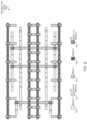
- a generalized block diagram of a top view of a standard cell layout 100is shown that utilizes techniques to reduce voltage droop.
- the standard cell layout 100is for a buffer with back-to-back inverters.
- the characteristics and techniques used for standard cell layout 100is used for a variety of other types of Boolean gates and complex gates.
- the p-type metal oxide semiconductor (PMOS) field effect transistors FETS (or pfets)are at the top of the standard cell layout 100 .
- the n-type metal oxide semiconductor (NMOS) FETS (or nfets)are at the bottom of the standard cell layout 100 .
- a “transistor”is also referred to as a “semiconductor device” or a “device.”
- the active region 190includes doped silicon for creating p-type transistors.
- the silicon substrate in the active region 190has been doped with Boron or Gallium during a semiconductor fabrication process.
- the active region 192includes doped silicon for creating n-type transistors.
- the silicon substrate in the active region 190has been doped with Phosphorous or Arsenic during a semiconductor fabrication process.
- the devices (or transistors) in the standard cell layout 100are non-planar devices.
- Non-planar transistorsare used in semiconductor processing for reducing short channel effects.
- Tri-gate transistors, Fin field effect transistors (FETs) and gate all around (GAA) transistorsare examples of non-planar transistors.
- the standard cell layout 100uses metal gate 110 in a vertical direction, metal 0 (M0 or Metal0) 130 for local interconnections in the horizontal direction, metal 1 (M1 or Metal1) 150 for local interconnections in the vertical direction, vias (or contacts) 152 for connecting the horizontal interconnect Metal0 130 to the vertical interconnect Metal1 150 , metal 2 (M2 or Metal2) 160 for horizontal power rails, and vias (or contacts) 162 for connecting the vertical interconnect Metal1 150 to the horizontal interconnect Metal2 160 .
- multiple layersare not shown, which are used to complete the circuitry of the back-to-back inverters of layout 100 . Examples of these layers are trench silicide contacts for the source and drain regions in the vertical direction, contacts for connecting the metal gate 110 to Metal0 130 , and contacts 142 for connecting the trench silicide contacts to Metal0 130 .
- metal gates 110used as dummy gates.
- Dummy gatesare typically used to provide electrical isolation between regions.
- a dummy gateuses a metal gate, the gate region is formed over an insulation layer, rather than an active silicon layer such as an n-type or p-type diffusion layer.
- the isolation layeruses a silicon nitride layer, a silicon oxide layer, such as a silicon dioxide layer, or another type of dielectric layer. Therefore, should voltage levels be applied on the dummy gate and one or more of the regions on either side of the dummy gate, such as source/drain regions, no electrical path is provided and no current flows between the source/drain regions.
- the fabrication steps for the dummy gateensures that an active transistor is not formed at the location in the layout of the dummy gate.
- standard cell layoutsuse dummy gates at the edges of the cell layout.
- dummy gatesare typically used to separate cells from one another. For example, an edge of a cell has a last active metal gate, followed by active diffusion, and then a dummy gate. In some designs, two adjacent cells share a dummy gate.
- the devices in the standard cell layout 100are fabricated by one of the immersion lithography techniques, the double patterning technique, the extreme ultraviolet lithography (EUV) technique, and the directed self-assembly (DSA) lithography technique.
- These techniquesprovide the resolution of each of the width and the pitch of the layout such as the horizontal Metal0 130 routes.
- the EUV techniqueuses an extreme ultraviolet wavelength to reach resolution below 40 nanometers.
- the extreme ultraviolet wavelengthis approximately 13.5 nanometers.
- the above techniques and newer techniquesare allowing a relatively high resolution for the width and the pitch of the other layout layers besides the horizontal Metal0 130 .
- the relatively high resolution for the width and the pitch of Metal1 150is obtained. Therefore, the maximum ratio of a number of vertical Metal1 150 tracks to a number of vertical metal gate 110 tracks can reduce to one.
- this ratio of a first number of Metal1 150 tracks that can fit in an area with a minimum width for Metal1 150 tracks to a second number of metal gate 110 tracks that can fit in the area with a minimum width for metal gate 110 tracks and still provide a processing yield above a thresholdis referred to as the “gear ratio”.
- Each of the first number and the second numberis a positive, non-zero integer.
- a two-to-one (2:1) gear ratiocan be achieved.
- a 2:1 gear ratioprovides a number of contacted gate pitches (CPP) for metal one power posts of one, or 1 CPP.
- the 2:1 gear ratioprovides a metal one power post between metal gates 110 and a metal one input or output signal over a metal gate 110 . Therefore, from a left edge of a metal gate 110 to a left edge of another metal gate 110 , there is space for two signals in the metal one layer 150 to be placed. With a single metal one power post between a pair of metal gates 110 , a metal one power post CPP of 1 is achieved. Although a few locations have been highlighted on layout 100 for using metal one power post CPP of 1 CPP, it is noted that it is possible and contemplated that each placement of a power post in Metal1 150 is capable of using 1 CPP.
- a metal one power post CPP of 1these power posts are also used for connections to a ground reference voltage level. Therefore, a metal one power post CPP applies to connections used for power supply voltage levels and to connections used for ground reference voltage levels.
- Layout 100uses horizontal Metal0 130 power rails underneath the horizontal Metal2 160 power rails. Layout 100 also uses minimum length vertical Metal1 150 power posts. The minimum length is set by design rules. As described above, these vertical Metal1 150 power posts are placed in a manner to achieve metal one power post CPP of 1 CPP for layout 100 . As the metal one power post CPP decreases from 4 CPP to 2 CPP to 1 CPP, the number of vias (contacts) 162 increases, so the overall resistance of vias 162 decreases. For example, the resistance of the vias 162 is halved with each reduction in the metal one power post CPP. The actual resistance of an individual via 162 remains the same.
- the overall resistance of all of the vias 162 used to connect the horizontal Metal2 160 power rails to the vertical Metal1 150 power postsreduces as the number of vias 162 increases. The same amount of current is being conducted from the horizontal Metal2 160 power rails to the vertical Metal1 150 power posts. However, as the overall resistance of all of the vias 162 decreases, the voltage droop also decreases.
- the layout 100uses 20 metal gates 110 between the dummy gates at the far ends.
- Four of the twenty metal gates 110are used for a first inverter of the back-to-back inverters that receives the input data, or input signal.
- Sixteen of the twenty metal gates 110are used for a second inverter of the back-to-back inverters that conveys the output data, or output signal.
- the “drive” of a standard cellis defined as a ratio of a number of metal gates 110 used to convey an output to a single metal gate 110 . This ratio provides a measurement of an amount of current that the standard cell consumes from the horizontal Metal2 160 power rails through the vertical Metal1 150 power posts to provide the output signal.
- This ratiois also referred to as the “drive” of the standard cell.
- the drive of the back-to-back inverters (or buffer) of layout 100is 16.
- the simultaneous switching of the metal gates 110 on the output node that causes current to be drawn from the horizontal Metal2 160 power rails through the vertical Metal1 150 power postscauses voltage droop.
- the placement of the vertical Metal1 150 power posts using metal one power post CPP of 1 CPPreduces voltage droop.
- the simultaneous switching of a wide buscauses a significant voltage drop if a supply pin served all of the line buffers on the bus.
- This voltage droop, ⁇ Vis proportional to the expression L di/dt, wherein L is the parasitic inductance and di/dt is the time rate of change of the current consumption. If a large number of nodes in addition to buses switched simultaneously, a significant voltage drop is possible. Now a node that holds a logic high value is capable of experiencing a voltage droop that reduces its voltage value below a minimum threshold. For memories and latches without recovery circuitry, it is possible for stored values to be lost.
- the use of placing the vertical Metal1 150 power posts with 1 CPPreduces the voltage droop. If the voltage droop is reduced to a value below a threshold value, then performance increases, data corruption is avoided, and the semiconductor fabrication process avoids using backside power rails and through silicon vias (TSVs) that are expensive.
- TSVsthrough silicon vias
- FIG. 2a generalized block diagram of a top view of a standard cell layout 200 is shown that utilizes techniques to reduce voltage droop. Layout elements and materials described earlier are numbered identically.
- the standard cell layout 200is for a buffer with back-to-back inverters.
- the characteristics and techniques used for standard cell layouts 100 (of FIG. 1 ) and 200are used for a variety of other types of Boolean gates and complex gates. Here, active regions are not shown for ease of illustration in the standard cell layout 200 . Similar to layout 100 (of FIG.
- the p-type devicesare formed at the top of the standard cell layout 200
- the n-type devicesare at the bottom of the standard cell layout 200 (or layout 200 ).
- the vertical Metal1 150 power postsare placed with 1 CPP.
- the vias (or contacts) 108 and the vias 132are shown.
- the vias 108connect the source regions implemented by trench silicide contacts (not shown) to the horizontal Metal0 130 layer.
- the vias 132connect the metal gate 110 to the horizontal Metal0 130 layer.
- Layout 200uses multiple power rails to provide a same voltage reference level.
- the two horizontal Metal2 160 power rails in the middle of layout 200provide a same first voltage reference level.
- This first voltage reference levelis one of multiple power supply voltage reference levels and ground reference voltage levels used by the circuitry of the buffer corresponding to the layout 200 .
- the two horizontal Metal2 160 power rails at the top of layout 200 and at the bottom of layout 200provide a same second voltage reference level.
- This second voltage reference levelis different from the first voltage reference level.
- This second voltage reference levelis one of multiple power supply voltage reference levels and ground reference voltage levels used by the circuitry of the buffer corresponding to the layout 200 .
- the layout 200uses a dual height approach.
- the layout 200has twice the height of the single height layout 100 (of FIG. 1 ) and half the width of the single height layout 100 .
- each of the horizontal Metal2 160 power railshas a reduced length and a smaller number of vertical Metal1 150 power posts connected to it for driving an output signal. Since the number of nodes capable of simultaneously switching is reduced, voltage droop is also reduced.
- the combination of placing the vertical Metal1 150 power posts with 1 CPP and using a dual height layout topology that reduces both the length and the via 162 connections on the horizontal Metal2 160 power railsgreatly reduces the voltage droop.
- FIG. 3a generalized block diagram of a top view of a standard cell layout 300 is shown that utilizes techniques to reduce voltage droop. Layout elements and materials described earlier are numbered identically.
- the standard cell layout 300is for a buffer with back-to-back inverters.
- the layout 300is the same as layout 200 , but some layout elements are removed for further ease of illustration. For example, the vias 108 and the vias 132 are removed.
- the placement of the vertical Metal1 150 power posts connected to the two horizontal Metal2 160 power rails at the top of layout 300 and at the bottom of layout 300include routing the vertical Metal1 150 power posts into the cell. This placement allows on-die area for neighboring cells to be placed.
- the placement of the vertical Metal1 150 power posts connected to the two horizontal Metal2 160 power rails in the middle of layout 300alternate between two Metal1 power posts routed into the cell and a single Metal1 power posts connecting the two Metal2 160 power rails to one another.
- Using a single Metal1 150 power postreduces capacitance for the power post and aids the conduction of current through the two Metal2 160 power rails.
- using two Metal1 150 power postsaids creating power connections in the cell.
- FIG. 4a generalized block diagram of a top view of a standard cell layout 400 is shown that utilizes techniques to reduce voltage droop.
- Layout elements and materials described earlierare numbered identically.
- the standard cell layout 400is for a buffer with back-to-back inverters.
- the layout 400is the same as layout 300 , but the placement of the vertical Metal1 150 power posts connected to the two horizontal Metal2 160 power rails in the middle of layout 400 do not alternate. Rather, each Metal1 150 power post is a single Metal1 power post connecting the two Metal2 160 power rails to one another.
- using a single Metal1 150 power postreduces capacitance for the power post and aids the conduction of current through the two Metal2 160 power rails. Therefore, voltage droop further reduces.
- FIG. 5a generalized block diagram of a top view of a standard cell layout 500 is shown that utilizes techniques to reduce voltage droop. Layout elements and materials described earlier are numbered identically. Similar to the layouts 100 - 400 , in the illustrated implementation, the standard cell layout 500 is for a buffer with back-to-back inverters. The layout 500 is the same as layout 400 , but the placement of the vertical Metal1 150 power posts connected to the two horizontal Metal2 160 power rails at the top of layout 500 and at the bottom of layout 500 uses metal one power post CPP of 2 CPP, rather than 1 CPP.
- the placement of the vertical Metal1 150 power posts at the top and the bottom of layout 500can use another value of metal one power post CPP besides 1 CPP.
- a placement using a metal one power post CPP of 2 CPPis shown.
- a placement using a metal one power post CPP of 3 CPP or otheris possible and contemplated.
- FIG. 6a generalized block diagram of a top view of a standard cell layout 600 is shown that utilizes techniques to reduce voltage droop. Layout elements and materials described earlier are numbered identically. Similar to the layouts 100 - 500 , in the illustrated implementation, the standard cell layout 600 is for a buffer with back-to-back inverters. However, in other implementations, the characteristics and techniques used for standard cell layouts 100 - 500 and 600 are used for a variety of other types of Boolean gates and complex gates. The layout 600 is the same as layout 500 , but the placement of the vertical Metal1 150 power posts connected to the two horizontal Metal2 160 power rails in the middle of layout 600 do not alternate.
- each Metal1 150 power postis a single Metal1 power post connecting the two Metal2 160 power rails to one another.
- using a single Metal1 150 power postreduces capacitance for the power post and aids the conduction of current through the two Metal2 160 power rails in the middle of the layout 600 . Therefore, voltage droop further reduces.
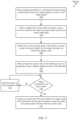
- FIG. 7one implementation of a method 700 is shown for efficiently creating a layout for a standard cell that utilizes techniques to reduce voltage droop.
- the steps in this implementationare shown in sequential order. However, in other implementations some steps occur in a different order than shown, some steps are performed concurrently, some steps are combined with other steps, and some steps are absent.
- One or more of a custom cell designer and an automated synthesis toolplaces multiple transistors in a standard cell layout using unidirectional tracks for routing signals in one or more metal layers (block 702 ).
- a single track of the metal one layer using a minimum width of the metal one layeris placed within a pitch of a single metal gate (block 704 ).
- power posts of the metal one layerare placed in a manner to achieve a metal one power post CPP of 1 CPP for layout of the standard cell.
- the metal one power post CPPdecreases from 4 CPP to 2 CPP to 1 CPP, the number of vias (contacts) used to connect the metal one power posts to the metal two power rails increases. As the number of these vias increases, the overall resistance of these vias decreases, which reduces the voltage droop.
- the methodis configured to route one or more power posts in the metal one layer using a minimum length for the metal one layer as defined by design rules (block 706 ).
- the minimum lengthreduces electromigration effects and provides area for signal routing for neighboring cells.
- a custom cell designer or an automated synthesis toolroutes, in a metal one track, the power posts using the minimum length.
- At least two power rails in the metal two layerare placed for supplying a same voltage reference level to the standard cell (block 708 ).
- the standard celluses a dual height approach with two metal two power rails in the middle of the standard cell and two other metal two power rails at the top and the bottom of the standard cell. The two middle metal two power rails provide a same first voltage reference to the standard cell.
- the first voltage reference levelis one of the multiple power supply voltage reference levels and the ground voltage reference levels used by the standard cell.
- the two metal two power rails at the top and the bottom of the standard cellprovide a same second voltage reference level to the standard cell that is different from the first voltage reference level.
- the standard celluses only the placement of metal one power posts with 1 CPP without using the dual height approach.
- the dual height approachis used, but a set of metal one power posts for a particular voltage reference level is not placed with 1 CPP, whereas, another set of metal one power posts for another voltage reference level is placed with 1 CPP.
- each of the metal one power posts connected to the two metal two power rails in the middle of the standard cellis connected to each of the metal two power rails.
- each of the metal one power posts connected to the two metal two power rails in the middle of the standard cellis connected to only one of the metal two power rails. Alternating between these connections of the metal one power posts in the middle of the standard cell is also possible and contemplated.
- the standard cellWhen the standard cell exists either as a netlist for circuit simulation or as a physical, fabricated cell on a silicon chip die, the standard cell does not generate a signal on an output node until the one or more power connections receive a power supply voltage, the one or more ground reference connections receive a ground reference voltage, and the one or more input nodes receive a potential such as Boolean logic level.
- the Boolean logic levelis one of a logic high level, such as the power supply voltage, or a logic low level such as the ground reference voltage. If a potential is not applied to an input node of the standard cell (“no” branch of the conditional block 710 ), then the standard cell waits for power up (block 712 ).
- the circuitry of the standard cellconveys a current from the input node to an output node of the standard cell through transistors using the metal one power posts and the metal two power rails (block 714 ).
- a computing system 800is shown with a processor that includes standard cells that utilize techniques to reduce voltage droop.
- the computing system 800includes the processor 810 and the memory 830 .
- Interfacessuch as a memory controller, a bus or a communication fabric, one or more phased locked loops (PLLs) and other clock generation circuitry, a power management unit, and so forth, are not shown for ease of illustration.
- PLLsphased locked loops
- the computing system 800includes one or more of other processors of a same type or a different type than processor 810 , one or more peripheral devices, a network interface, one or more other memory devices, and so forth.
- the functionality of the computing system 800is incorporated on a system on chip (SoC). In other implementations, the functionality of the computing system 800 is incorporated on a peripheral card inserted in a motherboard.
- SoCsystem on chip
- the computing system 800is used in any of a variety of computing devices such as a desktop computer, a tablet computer, a laptop, a smartphone, a smartwatch, a gaming console, a personal assistant device, and so forth.
- the processor 810includes hardware such as circuitry.
- the processor 810includes at least one integrated circuit 820 , which utilizes at least standard cell 822 .
- one or more standard cellsare instantiated in the integrated circuit 820 . These standard cells utilize the characteristics and techniques described earlier for standard cell layouts 100 - 600 (of FIGS. 1 - 6 ).
- the processor 810includes one or more processing units.
- each of the processing unitsincludes one or more processor cores capable of general-purpose data processing, and an associated cache memory subsystem.
- the processor 810is a central processing unit (CPU).
- the processing coresare compute units, each with a highly parallel data microarchitecture with multiple parallel execution lanes and an associated data storage buffer.
- the processor 810is a graphics processing unit (GPU), a digital signal processor (DSP), or other.
- the memory 830includes one or more of a hard disk drive, a solid-state disk, other types of flash memory, a portable solid-state drive, a tape drive and so on.
- the memory 830stores an operating system (OS) 832 , one or more applications represented by code 834 , and at least source data 836 .
- OSoperating system
- Memory 830is also capable of storing intermediate result data and final result data generated by the processor 810 when executing a particular application of code 834 .
- a single operating system 832 and a single instance of code 834 and source data 836are shown, in other implementations, another number of these software components are stored in memory 830 .
- the operating system 832includes instructions for initiating the boot up of the processor 810 , assigning tasks to hardware circuitry, managing resources of the computing system 800 and hosting one or more virtual environments.
- Each of the processor 810 and the memory 830includes an interface unit for communicating with one another as well as any other hardware components included in the computing system 800 .
- the interface unitsinclude queues for servicing memory requests and memory responses, and control circuitry for communicating with one another based on particular communication protocols.
- the communication protocolsdetermine a variety of parameters such as supply voltage levels, power-performance states that determine an operating supply voltage and an operating clock frequency, a data rate, one or more burst modes, and so on.
- a computer accessible storage mediumincludes any storage media accessible by a computer during use to provide instructions and/or data to the computer.
- a computer accessible storage mediumincludes storage media such as magnetic or optical media, e.g., disk (fixed or removable), tape, CD-ROM, or DVD-ROM, CD-R, CD-RW, DVD-R, DVD-RW, or Blu-Ray.
- Storage mediafurther includes volatile or non-volatile memory media such as RAM (e.g. synchronous dynamic RAM (SDRAM), double data rate (DDR, DDR2, DDR3, etc.) SDRAM, low-power DDR (LPDDR2, etc.) SDRAM, Rambus DRAM (RDRAM), static RAM (SRAM), etc.), ROM, Flash memory, non-volatile memory (e.g. Flash memory) accessible via a peripheral interface such as the Universal Serial Bus (USB) interface, etc.
- SDRAMsynchronous dynamic RAM
- DDRdouble data rate SDRAM
- LPDDR2, etc.low-power DDR
- RDRAMRambus DRAM
- SRAMstatic RAM
- ROMFlash memory
- non-volatile memorye.g. Flash memory
- USB
- program instructionsinclude behavioral-level descriptions or register-transfer level (RTL) descriptions of the hardware functionality in a high level programming language such as C, or a design language (HDL) such as Verilog, VHDL, or database format such as GDS II stream format (GDSII).
- RTLregister-transfer level
- HDLdesign language
- GDSIIdatabase format
- the descriptionis read by a synthesis tool, which synthesizes the description to produce a netlist including a list of gates from a synthesis library.
- the netlistincludes a set of gates, which also represent the functionality of the hardware including the system.
- the netlistis then placed and routed to produce a data set describing geometric shapes to be applied to masks.
- the masksare then used in various semiconductor fabrication steps to produce a semiconductor circuit or circuits corresponding to the system.
- the instructions on the computer accessible storage mediumare the netlist (with or without the synthesis library) or the data set, as desired. Additionally, the instructions are utilized for purposes of emulation by a hardware based type emulator from such vendors as Cadence®, EVE®, and Mentor Graphics®.
Landscapes
- Engineering & Computer Science (AREA)
- Physics & Mathematics (AREA)
- Computer Hardware Design (AREA)
- General Physics & Mathematics (AREA)
- Power Engineering (AREA)
- Microelectronics & Electronic Packaging (AREA)
- Condensed Matter Physics & Semiconductors (AREA)
- Geometry (AREA)
- Theoretical Computer Science (AREA)
- General Engineering & Computer Science (AREA)
- Computer Networks & Wireless Communication (AREA)
- Evolutionary Computation (AREA)
- Manufacturing & Machinery (AREA)
- Design And Manufacture Of Integrated Circuits (AREA)
Abstract
Description
Claims (20)
Priority Applications (6)
| Application Number | Priority Date | Filing Date | Title |
|---|---|---|---|
| US17/483,672US12205897B2 (en) | 2021-09-23 | 2021-09-23 | Standard cell design architecture for reduced voltage droop utilizing reduced contacted gate poly pitch and dual height cells |
| EP22783245.8AEP4406027A1 (en) | 2021-09-23 | 2022-09-09 | Standard cell design architecture for reduced voltage droop utilizing reduced contacted gate poly pitch and dual height cells |
| CN202280064040.5ACN117999651A (en) | 2021-09-23 | 2022-09-09 | Standard cell design architecture for reducing voltage drop with reduced contact gate polysilicon spacing and dual height cells |
| JP2024518310AJP2024538545A (en) | 2021-09-23 | 2022-09-09 | Standard Cell Design Architecture for Reduced Voltage Droop Utilizing Reduced Contact Gate Poly Pitch and Dual Height Cells |
| KR1020247012935AKR20240057441A (en) | 2021-09-23 | 2022-09-09 | Standard cell design architecture for reduced voltage droop utilizing reduced contact gate poly pitch and double height cells |
| PCT/US2022/076209WO2023049632A1 (en) | 2021-09-23 | 2022-09-09 | Standard cell design architecture for reduced voltage droop utilizing reduced contacted gate poly pitch and dual height cells |
Applications Claiming Priority (1)
| Application Number | Priority Date | Filing Date | Title |
|---|---|---|---|
| US17/483,672US12205897B2 (en) | 2021-09-23 | 2021-09-23 | Standard cell design architecture for reduced voltage droop utilizing reduced contacted gate poly pitch and dual height cells |
Publications (2)
| Publication Number | Publication Date |
|---|---|
| US20230092184A1 US20230092184A1 (en) | 2023-03-23 |
| US12205897B2true US12205897B2 (en) | 2025-01-21 |
Family
ID=83508809
Family Applications (1)
| Application Number | Title | Priority Date | Filing Date |
|---|---|---|---|
| US17/483,672Active2041-11-18US12205897B2 (en) | 2021-09-23 | 2021-09-23 | Standard cell design architecture for reduced voltage droop utilizing reduced contacted gate poly pitch and dual height cells |
Country Status (6)
| Country | Link |
|---|---|
| US (1) | US12205897B2 (en) |
| EP (1) | EP4406027A1 (en) |
| JP (1) | JP2024538545A (en) |
| KR (1) | KR20240057441A (en) |
| CN (1) | CN117999651A (en) |
| WO (1) | WO2023049632A1 (en) |
Families Citing this family (2)
| Publication number | Priority date | Publication date | Assignee | Title |
|---|---|---|---|---|
| US12100660B2 (en)* | 2021-10-04 | 2024-09-24 | Advanced Micro Devices, Inc. | Low congestion standard cells |
| US11848269B2 (en)* | 2021-10-04 | 2023-12-19 | Advanced Micro Devices, Inc. | Techniques to create power connections from floating nets in standard cells |
Citations (73)
| Publication number | Priority date | Publication date | Assignee | Title |
|---|---|---|---|---|
| US4851892A (en) | 1987-09-08 | 1989-07-25 | Motorola, Inc. | Standard cell array having fake gate for isolating devices from supply voltages |
| US5889329A (en) | 1994-11-02 | 1999-03-30 | Lsi Logic Corporation | Tri-directional interconnect architecture for SRAM |
| US6100101A (en) | 1998-10-27 | 2000-08-08 | Advanced Micro Devices Inc. | Sensitive technique for metal-void detection |
| US6242767B1 (en) | 1997-11-10 | 2001-06-05 | Lightspeed Semiconductor Corp. | Asic routing architecture |
| US20030023937A1 (en) | 2001-06-01 | 2003-01-30 | Mcmanus Michael J. | Method and apparatus for design of integrated circuits |
| US6609242B1 (en) | 2001-07-20 | 2003-08-19 | Hewlett-Packard Development Company, L.P. | Automated creation of power distribution grids for tiled cell arrays in integrated circuit designs |
| US20050212562A1 (en) | 2004-03-24 | 2005-09-29 | Jorg Gliese | Architecture of function blocks and wirings in a structured ASIC and configurable driver cell of a logic cell zone |
| US7064074B2 (en) | 2003-01-31 | 2006-06-20 | Advanced Micro Devices, Inc. | Technique for forming contacts for buried doped regions in a semiconductor device |
| US20070063244A1 (en) | 2005-09-22 | 2007-03-22 | International Business Machines Corporation | Trench metal-insulator-metal (mim) capacitors and method of fabricating same |
| WO2007073599A1 (en) | 2005-12-29 | 2007-07-05 | Mosaid Technologies Incorporated | Asic design using clock and power grid standard cell |
| US20070278528A1 (en) | 2006-06-01 | 2007-12-06 | Elpida Memory, Inc. | Semiconductor device |
| US20070284619A1 (en) | 2003-11-13 | 2007-12-13 | Yusuke Kanno | Semiconductor integrated circuit device |
| US20080283925A1 (en) | 2005-11-21 | 2008-11-20 | Joerg Berthold | Multi-Fin Component Arrangement and Method for Manufacturing a Multi-Fin Component Arrangement |
| US20090187871A1 (en) | 2008-01-17 | 2009-07-23 | Synopsys, Inc. | Hierarchical Compression For Metal One Logic Layer |
| US20100127333A1 (en) | 2008-11-21 | 2010-05-27 | Taiwan Semiconductor Manufacturing Company, Ltd. | novel layout architecture for performance enhancement |
| US20100148219A1 (en) | 2008-12-12 | 2010-06-17 | Renesas Technology Corp. | Semiconductor integrated circuit device |
| US20100287518A1 (en) | 2009-05-06 | 2010-11-11 | Tela Innovations, Inc. | Cell Circuit and Layout with Linear Finfet Structures |
| US8264007B2 (en) | 2006-03-09 | 2012-09-11 | Tela Innovations, Inc. | Semiconductor device including at least six transistor forming linear shapes including at least two different gate contact connection distances |
| US8356268B2 (en) | 2007-08-02 | 2013-01-15 | Tela Innovations, Inc. | Integrated circuit device including dynamic array section with gate level having linear conductive features on at least three side-by-side lines and uniform line end spacings |
| US20130026572A1 (en) | 2011-07-29 | 2013-01-31 | Synopsy, Inc. | N-channel and p-channel finfet cell architecture |
| US20130087834A1 (en) | 2011-10-07 | 2013-04-11 | Jonathan C. Park | Gate array architecture with multiple programmable regions |
| US20130146986A1 (en) | 2011-12-13 | 2013-06-13 | Globalfoundries Inc. | Semiconductor device with transistor local interconnects |
| US20130155753A1 (en) | 2011-12-19 | 2013-06-20 | SK Hynix Inc. | Method for implementing spare logic of semiconductor memory apparatus and structure thereof |
| US20130154128A1 (en) | 2011-12-20 | 2013-06-20 | Taiwan Semiconductor Manufacturing Co., Ltd. | Automatic Place and Route Method for Electromigration Tolerant Power Distribution |
| US8561003B2 (en) | 2011-07-29 | 2013-10-15 | Synopsys, Inc. | N-channel and P-channel finFET cell architecture with inter-block insulator |
| US20130295756A1 (en) | 2012-05-07 | 2013-11-07 | Globalfoundries Inc. | Methods of forming contacts for semiconductor devices using a local interconnect processing scheme |
| US20130313513A1 (en) | 2011-12-23 | 2013-11-28 | Annalisa Cappellani | Semiconductor devices having modulated nanowire counts |
| US20130334613A1 (en) | 2012-06-13 | 2013-12-19 | Synopsys, Inc. | N-channel and p-channel end-to-end finfet cell architecture |
| US8680626B2 (en) | 2007-10-26 | 2014-03-25 | Tela Innovations, Inc. | Methods, structures, and designs for self-aligning local interconnects used in integrated circuits |
| US20140145342A1 (en) | 2012-11-27 | 2014-05-29 | Advanced Micro Devices, Inc. | Metal density distribution for double pattern lithography |
| US20140252650A1 (en) | 2013-03-08 | 2014-09-11 | Kabushiki Kaisha Toshiba | Semiconductor integrated circuit |
| US20140264742A1 (en) | 2013-03-14 | 2014-09-18 | Taiwan Semiconductor Manufacturing Company, Ltd. | Integrated Capacitor |
| US20150052494A1 (en) | 2013-08-16 | 2015-02-19 | Globalfoundries Inc. | Power rail layout for dense standard cell library |
| US20150048425A1 (en) | 2011-10-07 | 2015-02-19 | Baysand Inc. | Gate array architecture with multiple programmable regions |
| US20150069531A1 (en) | 2013-09-06 | 2015-03-12 | International Business Machines Corporation | Locally raised epitaxy for improved contact by local silicon capping during trench silicide processings |
| US20150269302A1 (en) | 2014-03-18 | 2015-09-24 | Taiwan Semiconductor Manufacturing Company Ltd. | Electromigration-aware layout generation |
| US20150302917A1 (en) | 2014-04-17 | 2015-10-22 | Stmicroelectronics International N.V. | SRAM Cell and Cell Layout Method |
| US20160163644A1 (en) | 2014-12-05 | 2016-06-09 | Globalfoundries Inc. | Merged source/drain and gate contacts in sram bitcell |
| US9400862B2 (en) | 2014-06-23 | 2016-07-26 | Synopsys, Inc. | Cells having transistors and interconnects including nanowires or 2D material strips |
| US9431383B2 (en) | 2014-07-22 | 2016-08-30 | Samsung Electronics Co., Ltd. | Integrated circuit, semiconductor device based on integrated circuit, and standard cell library |
| US20160276287A1 (en) | 2013-12-06 | 2016-09-22 | Renesas Electronics Corporation | Semiconductor device |
| US20160284705A1 (en) | 2015-03-25 | 2016-09-29 | Jae-Yup Chung | Integrated circuit device and method of manufacturing the same |
| US9460259B2 (en) | 2014-08-22 | 2016-10-04 | Samsung Electronics Co., Ltd. | Methods of generating integrated circuit layout using standard cell library |
| US9502351B1 (en) | 2015-09-15 | 2016-11-22 | Qualcomm Incorporated | Multiple split rail standard cell library architecture |
| US20170011999A1 (en) | 2015-07-08 | 2017-01-12 | Samsung Electronics Co., Ltd. | Semiconductor integrated circuit and electronic system including the same |
| US9553028B2 (en) | 2014-03-19 | 2017-01-24 | Globalfoundries Inc. | Methods of forming reduced resistance local interconnect structures and the resulting devices |
| US9589847B1 (en) | 2016-02-18 | 2017-03-07 | International Business Machines Corporation | Metal layer tip to tip short |
| US9633987B2 (en) | 2007-03-05 | 2017-04-25 | Tela Innovations, Inc. | Integrated circuit cell library for multiple patterning |
| US20170125292A1 (en) | 2015-10-30 | 2017-05-04 | International Business Machines Corporation | Trench silicide contacts with high selectivity process |
| US9659939B1 (en) | 2015-11-30 | 2017-05-23 | International Business Machines Corporation | Integrated circuit having MIM capacitor with refractory metal silicided strap and method to fabricate same |
| US20170154848A1 (en) | 2015-11-30 | 2017-06-01 | Taiwan Semiconductor Manufacturing Co., Ltd. | Standard-cell layout structure with horn power and smart metal cut |
| US9691768B2 (en) | 2014-06-23 | 2017-06-27 | Synopsys, Inc. | Nanowire or 2D material strips interconnects in an integrated circuit cell |
| US9704995B1 (en) | 2016-09-20 | 2017-07-11 | Advanced Micro Devices, Inc. | Gate all around device architecture with local oxide |
| US20170263506A1 (en) | 2016-03-11 | 2017-09-14 | Globalfoundries Inc. | Methods, apparatus and system for a passthrough-based architecture |
| US20170294448A1 (en) | 2016-04-06 | 2017-10-12 | Imec Vzw | Integrated circuit power distribution network |
| US20170323902A1 (en) | 2016-05-06 | 2017-11-09 | Globalfoundries Inc. | Method, apparatus, and system for improved cell design having unidirectional metal layout architecture |
| US9837398B1 (en) | 2016-11-23 | 2017-12-05 | Advanced Micro Devices, Inc. | Metal track cutting in standard cell layouts |
| US20170373090A1 (en) | 2016-06-22 | 2017-12-28 | Qualcomm Incorporated | Standard cell architecture for diffusion based on fin count |
| US20180040631A1 (en) | 2016-08-02 | 2018-02-08 | Globalfoundries Inc. | Method, apparatus, and system for improved memory cell design having unidirectional layout using self-aligned double patterning |
| US20180090440A1 (en) | 2016-09-23 | 2018-03-29 | Advanced Micro Devices, Inc. | Power grid layout designs for integrated circuits |
| US20180183414A1 (en) | 2016-12-28 | 2018-06-28 | Taiwan Semiconductor Manufacturing Co., Ltd. | Cell of transmission gate free circuit and integrated circuit layout including the same |
| US20180190670A1 (en) | 2016-12-29 | 2018-07-05 | Imec Vzw | Standard cell having vertical transistors |
| US20180218981A1 (en) | 2017-01-27 | 2018-08-02 | Globalfoundries Inc. | Circuit design having aligned power staples |
| US20180315709A1 (en) | 2017-05-01 | 2018-11-01 | Advanced Micro Devices, Inc. | Standard cell layout architectures and drawing styles for 5nm and beyond |
| US20180314785A1 (en) | 2017-05-01 | 2018-11-01 | Advanced Micro Devices, Inc. | Power grid architecture and optimization with euv lithography |
| US20190065650A1 (en) | 2017-08-30 | 2019-02-28 | Arm Limited | Integrated circuit design and/or fabrication |
| US20190155979A1 (en) | 2017-11-21 | 2019-05-23 | Advanced Micro Devices, Inc. | Metal zero power ground stub route to reduce cell area and improve cell placement at the chip level |
| US10438937B1 (en) | 2018-04-27 | 2019-10-08 | Advanced Micro Devices, Inc. | Metal zero contact via redundancy on output nodes and inset power rail architecture |
| US20190363167A1 (en) | 2018-05-25 | 2019-11-28 | Advanced Micro Devices, Inc. | Gate contact over active region in cell |
| US20190385999A1 (en) | 2018-06-15 | 2019-12-19 | Samsung Electronics Co., Ltd. | Power grid and standard cell co-design structure and methods thereof |
| US20200019666A1 (en) | 2018-07-16 | 2020-01-16 | Taiwan Semiconductor Manufacturing Company, Ltd. | Tap cells |
| US10796061B1 (en)* | 2019-08-29 | 2020-10-06 | Advanced Micro Devices, Inc. | Standard cell and power grid architectures with EUV lithography |
| US11742289B2 (en) | 2019-04-12 | 2023-08-29 | Advanced Micro Devices, Inc. | Semiconductor chip with stacked conductor lines and air gaps |
- 2021
- 2021-09-23USUS17/483,672patent/US12205897B2/enactiveActive
- 2022
- 2022-09-09CNCN202280064040.5Apatent/CN117999651A/enactivePending
- 2022-09-09JPJP2024518310Apatent/JP2024538545A/enactivePending
- 2022-09-09WOPCT/US2022/076209patent/WO2023049632A1/ennot_activeCeased
- 2022-09-09EPEP22783245.8Apatent/EP4406027A1/enactivePending
- 2022-09-09KRKR1020247012935Apatent/KR20240057441A/enactivePending
Patent Citations (79)
| Publication number | Priority date | Publication date | Assignee | Title |
|---|---|---|---|---|
| US4851892A (en) | 1987-09-08 | 1989-07-25 | Motorola, Inc. | Standard cell array having fake gate for isolating devices from supply voltages |
| US5889329A (en) | 1994-11-02 | 1999-03-30 | Lsi Logic Corporation | Tri-directional interconnect architecture for SRAM |
| US6242767B1 (en) | 1997-11-10 | 2001-06-05 | Lightspeed Semiconductor Corp. | Asic routing architecture |
| US6100101A (en) | 1998-10-27 | 2000-08-08 | Advanced Micro Devices Inc. | Sensitive technique for metal-void detection |
| US20030023937A1 (en) | 2001-06-01 | 2003-01-30 | Mcmanus Michael J. | Method and apparatus for design of integrated circuits |
| US6609242B1 (en) | 2001-07-20 | 2003-08-19 | Hewlett-Packard Development Company, L.P. | Automated creation of power distribution grids for tiled cell arrays in integrated circuit designs |
| US7064074B2 (en) | 2003-01-31 | 2006-06-20 | Advanced Micro Devices, Inc. | Technique for forming contacts for buried doped regions in a semiconductor device |
| US20070284619A1 (en) | 2003-11-13 | 2007-12-13 | Yusuke Kanno | Semiconductor integrated circuit device |
| US20050212562A1 (en) | 2004-03-24 | 2005-09-29 | Jorg Gliese | Architecture of function blocks and wirings in a structured ASIC and configurable driver cell of a logic cell zone |
| US20070063244A1 (en) | 2005-09-22 | 2007-03-22 | International Business Machines Corporation | Trench metal-insulator-metal (mim) capacitors and method of fabricating same |
| US20080283925A1 (en) | 2005-11-21 | 2008-11-20 | Joerg Berthold | Multi-Fin Component Arrangement and Method for Manufacturing a Multi-Fin Component Arrangement |
| US20070157144A1 (en) | 2005-12-29 | 2007-07-05 | Tony Mai | ASIC design using clock and power grid standard cell |
| WO2007073599A1 (en) | 2005-12-29 | 2007-07-05 | Mosaid Technologies Incorporated | Asic design using clock and power grid standard cell |
| US8264007B2 (en) | 2006-03-09 | 2012-09-11 | Tela Innovations, Inc. | Semiconductor device including at least six transistor forming linear shapes including at least two different gate contact connection distances |
| US20170365621A1 (en) | 2006-03-09 | 2017-12-21 | Tela Innovations, Inc. | Semiconductor Chip and Method for Manufacturing the Same |
| US20070278528A1 (en) | 2006-06-01 | 2007-12-06 | Elpida Memory, Inc. | Semiconductor device |
| US9633987B2 (en) | 2007-03-05 | 2017-04-25 | Tela Innovations, Inc. | Integrated circuit cell library for multiple patterning |
| US8356268B2 (en) | 2007-08-02 | 2013-01-15 | Tela Innovations, Inc. | Integrated circuit device including dynamic array section with gate level having linear conductive features on at least three side-by-side lines and uniform line end spacings |
| US8680626B2 (en) | 2007-10-26 | 2014-03-25 | Tela Innovations, Inc. | Methods, structures, and designs for self-aligning local interconnects used in integrated circuits |
| US20090187871A1 (en) | 2008-01-17 | 2009-07-23 | Synopsys, Inc. | Hierarchical Compression For Metal One Logic Layer |
| US20100127333A1 (en) | 2008-11-21 | 2010-05-27 | Taiwan Semiconductor Manufacturing Company, Ltd. | novel layout architecture for performance enhancement |
| US20100148219A1 (en) | 2008-12-12 | 2010-06-17 | Renesas Technology Corp. | Semiconductor integrated circuit device |
| US20100287518A1 (en) | 2009-05-06 | 2010-11-11 | Tela Innovations, Inc. | Cell Circuit and Layout with Linear Finfet Structures |
| US20130026572A1 (en) | 2011-07-29 | 2013-01-31 | Synopsy, Inc. | N-channel and p-channel finfet cell architecture |
| US8561003B2 (en) | 2011-07-29 | 2013-10-15 | Synopsys, Inc. | N-channel and P-channel finFET cell architecture with inter-block insulator |
| US20130087834A1 (en) | 2011-10-07 | 2013-04-11 | Jonathan C. Park | Gate array architecture with multiple programmable regions |
| US20150048425A1 (en) | 2011-10-07 | 2015-02-19 | Baysand Inc. | Gate array architecture with multiple programmable regions |
| US20130146986A1 (en) | 2011-12-13 | 2013-06-13 | Globalfoundries Inc. | Semiconductor device with transistor local interconnects |
| US20130155753A1 (en) | 2011-12-19 | 2013-06-20 | SK Hynix Inc. | Method for implementing spare logic of semiconductor memory apparatus and structure thereof |
| US20130154128A1 (en) | 2011-12-20 | 2013-06-20 | Taiwan Semiconductor Manufacturing Co., Ltd. | Automatic Place and Route Method for Electromigration Tolerant Power Distribution |
| US20130313513A1 (en) | 2011-12-23 | 2013-11-28 | Annalisa Cappellani | Semiconductor devices having modulated nanowire counts |
| US20130295756A1 (en) | 2012-05-07 | 2013-11-07 | Globalfoundries Inc. | Methods of forming contacts for semiconductor devices using a local interconnect processing scheme |
| US20130334613A1 (en) | 2012-06-13 | 2013-12-19 | Synopsys, Inc. | N-channel and p-channel end-to-end finfet cell architecture |
| US20140145342A1 (en) | 2012-11-27 | 2014-05-29 | Advanced Micro Devices, Inc. | Metal density distribution for double pattern lithography |
| US20140252650A1 (en) | 2013-03-08 | 2014-09-11 | Kabushiki Kaisha Toshiba | Semiconductor integrated circuit |
| US20140264742A1 (en) | 2013-03-14 | 2014-09-18 | Taiwan Semiconductor Manufacturing Company, Ltd. | Integrated Capacitor |
| US20150052494A1 (en) | 2013-08-16 | 2015-02-19 | Globalfoundries Inc. | Power rail layout for dense standard cell library |
| US20150069531A1 (en) | 2013-09-06 | 2015-03-12 | International Business Machines Corporation | Locally raised epitaxy for improved contact by local silicon capping during trench silicide processings |
| US20160276287A1 (en) | 2013-12-06 | 2016-09-22 | Renesas Electronics Corporation | Semiconductor device |
| US20150269302A1 (en) | 2014-03-18 | 2015-09-24 | Taiwan Semiconductor Manufacturing Company Ltd. | Electromigration-aware layout generation |
| US9553028B2 (en) | 2014-03-19 | 2017-01-24 | Globalfoundries Inc. | Methods of forming reduced resistance local interconnect structures and the resulting devices |
| US20150302917A1 (en) | 2014-04-17 | 2015-10-22 | Stmicroelectronics International N.V. | SRAM Cell and Cell Layout Method |
| US9400862B2 (en) | 2014-06-23 | 2016-07-26 | Synopsys, Inc. | Cells having transistors and interconnects including nanowires or 2D material strips |
| US9691768B2 (en) | 2014-06-23 | 2017-06-27 | Synopsys, Inc. | Nanowire or 2D material strips interconnects in an integrated circuit cell |
| US9431383B2 (en) | 2014-07-22 | 2016-08-30 | Samsung Electronics Co., Ltd. | Integrated circuit, semiconductor device based on integrated circuit, and standard cell library |
| US9837437B2 (en) | 2014-07-22 | 2017-12-05 | Samsung Electronics Co., Ltd. | Integrated circuit, semiconductor device based on integrated circuit, and standard cell library |
| US9460259B2 (en) | 2014-08-22 | 2016-10-04 | Samsung Electronics Co., Ltd. | Methods of generating integrated circuit layout using standard cell library |
| US20160163644A1 (en) | 2014-12-05 | 2016-06-09 | Globalfoundries Inc. | Merged source/drain and gate contacts in sram bitcell |
| US20160284705A1 (en) | 2015-03-25 | 2016-09-29 | Jae-Yup Chung | Integrated circuit device and method of manufacturing the same |
| US20170011999A1 (en) | 2015-07-08 | 2017-01-12 | Samsung Electronics Co., Ltd. | Semiconductor integrated circuit and electronic system including the same |
| US9502351B1 (en) | 2015-09-15 | 2016-11-22 | Qualcomm Incorporated | Multiple split rail standard cell library architecture |
| US20170125292A1 (en) | 2015-10-30 | 2017-05-04 | International Business Machines Corporation | Trench silicide contacts with high selectivity process |
| US9659939B1 (en) | 2015-11-30 | 2017-05-23 | International Business Machines Corporation | Integrated circuit having MIM capacitor with refractory metal silicided strap and method to fabricate same |
| US20170154848A1 (en) | 2015-11-30 | 2017-06-01 | Taiwan Semiconductor Manufacturing Co., Ltd. | Standard-cell layout structure with horn power and smart metal cut |
| US9589847B1 (en) | 2016-02-18 | 2017-03-07 | International Business Machines Corporation | Metal layer tip to tip short |
| US20170263506A1 (en) | 2016-03-11 | 2017-09-14 | Globalfoundries Inc. | Methods, apparatus and system for a passthrough-based architecture |
| US20180033701A1 (en) | 2016-03-11 | 2018-02-01 | Globalfoundries Inc. | Methods, apparatus and system for a passthrough-based architecture |
| US20170294448A1 (en) | 2016-04-06 | 2017-10-12 | Imec Vzw | Integrated circuit power distribution network |
| US20170323902A1 (en) | 2016-05-06 | 2017-11-09 | Globalfoundries Inc. | Method, apparatus, and system for improved cell design having unidirectional metal layout architecture |
| US20170371995A1 (en) | 2016-06-22 | 2017-12-28 | Qualcomm Incorporated | Standard cell architecture for diffusion based on fin count |
| US20170373090A1 (en) | 2016-06-22 | 2017-12-28 | Qualcomm Incorporated | Standard cell architecture for diffusion based on fin count |
| US20180040631A1 (en) | 2016-08-02 | 2018-02-08 | Globalfoundries Inc. | Method, apparatus, and system for improved memory cell design having unidirectional layout using self-aligned double patterning |
| US9704995B1 (en) | 2016-09-20 | 2017-07-11 | Advanced Micro Devices, Inc. | Gate all around device architecture with local oxide |
| US20180090440A1 (en) | 2016-09-23 | 2018-03-29 | Advanced Micro Devices, Inc. | Power grid layout designs for integrated circuits |
| US9837398B1 (en) | 2016-11-23 | 2017-12-05 | Advanced Micro Devices, Inc. | Metal track cutting in standard cell layouts |
| US20180183414A1 (en) | 2016-12-28 | 2018-06-28 | Taiwan Semiconductor Manufacturing Co., Ltd. | Cell of transmission gate free circuit and integrated circuit layout including the same |
| US20180190670A1 (en) | 2016-12-29 | 2018-07-05 | Imec Vzw | Standard cell having vertical transistors |
| US20180218981A1 (en) | 2017-01-27 | 2018-08-02 | Globalfoundries Inc. | Circuit design having aligned power staples |
| US20180315709A1 (en) | 2017-05-01 | 2018-11-01 | Advanced Micro Devices, Inc. | Standard cell layout architectures and drawing styles for 5nm and beyond |
| US20180314785A1 (en) | 2017-05-01 | 2018-11-01 | Advanced Micro Devices, Inc. | Power grid architecture and optimization with euv lithography |
| US20190065650A1 (en) | 2017-08-30 | 2019-02-28 | Arm Limited | Integrated circuit design and/or fabrication |
| US20190155979A1 (en) | 2017-11-21 | 2019-05-23 | Advanced Micro Devices, Inc. | Metal zero power ground stub route to reduce cell area and improve cell placement at the chip level |
| US10438937B1 (en) | 2018-04-27 | 2019-10-08 | Advanced Micro Devices, Inc. | Metal zero contact via redundancy on output nodes and inset power rail architecture |
| US20190363167A1 (en) | 2018-05-25 | 2019-11-28 | Advanced Micro Devices, Inc. | Gate contact over active region in cell |
| US20190385999A1 (en) | 2018-06-15 | 2019-12-19 | Samsung Electronics Co., Ltd. | Power grid and standard cell co-design structure and methods thereof |
| US20200019666A1 (en) | 2018-07-16 | 2020-01-16 | Taiwan Semiconductor Manufacturing Company, Ltd. | Tap cells |
| US11742289B2 (en) | 2019-04-12 | 2023-08-29 | Advanced Micro Devices, Inc. | Semiconductor chip with stacked conductor lines and air gaps |
| US10796061B1 (en)* | 2019-08-29 | 2020-10-06 | Advanced Micro Devices, Inc. | Standard cell and power grid architectures with EUV lithography |
| WO2021041687A1 (en) | 2019-08-29 | 2021-03-04 | Advanced Micro Devices, Inc. | Standard cell and power grid architectures with euv lithography |
Non-Patent Citations (14)
| Title |
|---|
| Cui et al., "7nm FinFET Standard Cell Layout Characterization and Power Density Prediction in Near- and Super-Threshold Voltage Regimes", International Green Computing Conference, Nov. 2014, 7 pages. |
| Final Office Action in U.S. Appl. No. 15/275,028, dated May 16, 2019, 12 pages. |
| Final Office Action in U.S. Appl. No. 15/636,245, dated Jan. 14, 2019, 31 pages. |
| International Search Report and Written Opinion in International Application No. PCT/US2017/052775, dated Mar. 26, 2018, 17 pages. |
| International Search Report and Written Opinion in International Application No. PCT/US2018/029760, dated Jul. 16, 2018, 16 pages. |
| International Search Report and Written Opinion in International Application No. PCT/US2018/029767, dated Jul. 11, 2018, 14 pages. |
| International Search Report and Written Opinion in International Application No. PCT/US2018/052369, dated Jan. 7, 2019, 16 pages. |
| International Search Report and Written Opinion in International Application No. PCT/US2022/076209, dated Dec. 21, 2022, 11 pages. |
| Non-Final Office Action in U.S. Appl. No. 15/275,028, dated Sep. 28, 2018, 10 pages. |
| Non-Final Office Action in U.S. Appl. No. 15/636,245, dated May 18, 2018, 30 pages. |
| Non-Final Office Action in U.S. Appl. No. 15/636,245, dated May 29, 2019, 23 pages. |
| Non-Final Office Action in U.S. Appl. No. 15/636,278, dated Apr. 5, 2019, 12 pages. |
| Non-Final Office Action in U.S. Appl. No. 15/819,879, dated Mar. 18, 2019, 10 pages. |
| Xie et al., "5nm FinFET Standard Cell Library Optimization and Circuit Synthesis in Near- and Super-Threshold Voltage Regimes", 2014 IEEE Computer Society Annual Symposium on VLSI, Jul. 2014, pp. 424-429. |
Also Published As
| Publication number | Publication date |
|---|---|
| CN117999651A (en) | 2024-05-07 |
| WO2023049632A1 (en) | 2023-03-30 |
| US20230092184A1 (en) | 2023-03-23 |
| EP4406027A1 (en) | 2024-07-31 |
| JP2024538545A (en) | 2024-10-23 |
| KR20240057441A (en) | 2024-05-02 |
Similar Documents
| Publication | Publication Date | Title |
|---|---|---|
| JP7668763B2 (en) | METAL ZERO POWER GROUND STUB ROUTE FOR REDUCING CELL AREA AND IMPROVING CELL PLACEMENT AT CHIP LEVEL | |
| US11347925B2 (en) | Power grid architecture and optimization with EUV lithography | |
| US10438937B1 (en) | Metal zero contact via redundancy on output nodes and inset power rail architecture | |
| KR102657056B1 (en) | Standard cell and power grid architecture using EUV lithography | |
| US11862640B2 (en) | Cross field effect transistor (XFET) library architecture power routing | |
| US12205897B2 (en) | Standard cell design architecture for reduced voltage droop utilizing reduced contacted gate poly pitch and dual height cells | |
| US20240258322A1 (en) | Cross field effect transistor library cell architecture design | |
| US12100660B2 (en) | Low congestion standard cells | |
| US11848269B2 (en) | Techniques to create power connections from floating nets in standard cells | |
| US20240113022A1 (en) | Power via with reduced resistance | |
| US20240128192A1 (en) | Backside power with on-die power switches | |
| US20240403529A1 (en) | Zero diffusion break between standard cells using three-dimensional cross field effect self-aligned transistors | |
| US20240162320A1 (en) | Three-dimensional cross field effect self-aligned transistors with frontside and backside power connections | |
| US20240038596A1 (en) | Double side transistors on same silicon wafer | |
| Lim et al. | 15 Design Challenges |
Legal Events
| Date | Code | Title | Description |
|---|---|---|---|
| AS | Assignment | Owner name:ADVANCED MICRO DEVICES, INC., CALIFORNIA Free format text:ASSIGNMENT OF ASSIGNORS INTEREST;ASSIGNOR:SCHULTZ, RICHARD T.;REEL/FRAME:057596/0988 Effective date:20210923 | |
| FEPP | Fee payment procedure | Free format text:ENTITY STATUS SET TO UNDISCOUNTED (ORIGINAL EVENT CODE: BIG.); ENTITY STATUS OF PATENT OWNER: LARGE ENTITY | |
| STPP | Information on status: patent application and granting procedure in general | Free format text:DOCKETED NEW CASE - READY FOR EXAMINATION | |
| STPP | Information on status: patent application and granting procedure in general | Free format text:EX PARTE QUAYLE ACTION MAILED | |
| STPP | Information on status: patent application and granting procedure in general | Free format text:RESPONSE TO EX PARTE QUAYLE ACTION ENTERED AND FORWARDED TO EXAMINER | |
| STPP | Information on status: patent application and granting procedure in general | Free format text:NOTICE OF ALLOWANCE MAILED -- APPLICATION RECEIVED IN OFFICE OF PUBLICATIONS | |
| ZAAA | Notice of allowance and fees due | Free format text:ORIGINAL CODE: NOA | |
| ZAAB | Notice of allowance mailed | Free format text:ORIGINAL CODE: MN/=. | |
| STPP | Information on status: patent application and granting procedure in general | Free format text:DOCKETED NEW CASE - READY FOR EXAMINATION | |
| STPP | Information on status: patent application and granting procedure in general | Free format text:NON FINAL ACTION MAILED | |
| STPP | Information on status: patent application and granting procedure in general | Free format text:RESPONSE TO NON-FINAL OFFICE ACTION ENTERED AND FORWARDED TO EXAMINER | |
| STPP | Information on status: patent application and granting procedure in general | Free format text:NOTICE OF ALLOWANCE MAILED -- APPLICATION RECEIVED IN OFFICE OF PUBLICATIONS | |
| ZAAB | Notice of allowance mailed | Free format text:ORIGINAL CODE: MN/=. | |
| STPP | Information on status: patent application and granting procedure in general | Free format text:PUBLICATIONS -- ISSUE FEE PAYMENT VERIFIED | |
| STCF | Information on status: patent grant | Free format text:PATENTED CASE | |
| CC | Certificate of correction |