US12204155B2 - Chip-to-chip optical coupling for photonic integrated circuits - Google Patents
Chip-to-chip optical coupling for photonic integrated circuitsDownload PDFInfo
- Publication number
- US12204155B2 US12204155B2US17/850,828US202217850828AUS12204155B2US 12204155 B2US12204155 B2US 12204155B2US 202217850828 AUS202217850828 AUS 202217850828AUS 12204155 B2US12204155 B2US 12204155B2
- Authority
- US
- United States
- Prior art keywords
- chip
- photonic
- channel
- protrusion
- circuit element
- Prior art date
- Legal status (The legal status is an assumption and is not a legal conclusion. Google has not performed a legal analysis and makes no representation as to the accuracy of the status listed.)
- Active
Links
- 230000003287optical effectEffects0.000titleclaimsdescription21
- 230000008878couplingEffects0.000titleclaimsdescription15
- 238000010168coupling processMethods0.000titleclaimsdescription15
- 238000005859coupling reactionMethods0.000titleclaimsdescription15
- 238000000034methodMethods0.000claimsabstractdescription50
- 230000000295complement effectEffects0.000claimsabstractdescription39
- 238000000206photolithographyMethods0.000claimsabstractdescription11
- 238000004519manufacturing processMethods0.000claimsdescription20
- 229910052710siliconInorganic materials0.000claimsdescription8
- 239000010703siliconSubstances0.000claimsdescription8
- 239000000758substrateSubstances0.000description39
- 238000010586diagramMethods0.000description11
- 238000010276constructionMethods0.000description9
- XUIMIQQOPSSXEZ-UHFFFAOYSA-NSiliconChemical compound[Si]XUIMIQQOPSSXEZ-UHFFFAOYSA-N0.000description7
- 230000013011matingEffects0.000description7
- 239000010410layerSubstances0.000description5
- 238000012986modificationMethods0.000description5
- 230000004048modificationEffects0.000description5
- 229910000679solderInorganic materials0.000description5
- 239000004065semiconductorSubstances0.000description4
- 230000000694effectsEffects0.000description2
- 239000000463materialSubstances0.000description2
- 229910052581Si3N4Inorganic materials0.000description1
- 238000007796conventional methodMethods0.000description1
- 230000009977dual effectEffects0.000description1
- 230000007717exclusionEffects0.000description1
- 238000003384imaging methodMethods0.000description1
- 239000002346layers by functionSubstances0.000description1
- 230000010287polarizationEffects0.000description1
- 230000000750progressive effectEffects0.000description1
- 238000000926separation methodMethods0.000description1
- HQVNEWCFYHHQES-UHFFFAOYSA-Nsilicon nitrideChemical compoundN12[Si]34N5[Si]62N3[Si]51N64HQVNEWCFYHHQES-UHFFFAOYSA-N0.000description1
- 238000012546transferMethods0.000description1
Images


Classifications
- G—PHYSICS
- G02—OPTICS
- G02B—OPTICAL ELEMENTS, SYSTEMS OR APPARATUS
- G02B6/00—Light guides; Structural details of arrangements comprising light guides and other optical elements, e.g. couplings
- G02B6/24—Coupling light guides
- G02B6/42—Coupling light guides with opto-electronic elements
- G02B6/4201—Packages, e.g. shape, construction, internal or external details
- G02B6/4219—Mechanical fixtures for holding or positioning the elements relative to each other in the couplings; Alignment methods for the elements, e.g. measuring or observing methods especially used therefor
- G02B6/4228—Passive alignment, i.e. without a detection of the degree of coupling or the position of the elements
- G02B6/423—Passive alignment, i.e. without a detection of the degree of coupling or the position of the elements using guiding surfaces for the alignment
- G—PHYSICS
- G02—OPTICS
- G02B—OPTICAL ELEMENTS, SYSTEMS OR APPARATUS
- G02B6/00—Light guides; Structural details of arrangements comprising light guides and other optical elements, e.g. couplings
- G02B6/24—Coupling light guides
- G02B6/42—Coupling light guides with opto-electronic elements
- G02B6/4201—Packages, e.g. shape, construction, internal or external details
- G02B6/4219—Mechanical fixtures for holding or positioning the elements relative to each other in the couplings; Alignment methods for the elements, e.g. measuring or observing methods especially used therefor
- G02B6/4228—Passive alignment, i.e. without a detection of the degree of coupling or the position of the elements
- G02B6/4232—Passive alignment, i.e. without a detection of the degree of coupling or the position of the elements using the surface tension of fluid solder to align the elements, e.g. solder bump techniques
Definitions
- Embodiments described hereinrelate to photonic integrated circuits and, in particular, to systems and methods providing accurate and precise alignment when optically intercoupling photonic circuits defined on separate chips.
- a photonic integrated circuitcan include multiple circuit elements, each formed by different manufacturing processes. Some manufacturing processes are incompatible, so in some cases, a circuit element formed in a first process may be optically and/or mechanically coupled to a second circuit element formed separately in a second process. For example, a laser element formed onto a substrate may be mechanically and optically coupled to a waveguide formed in a separate process onto a different substrate.
- Embodiments described hereinreference systems and methods for effective precise and accurate lateral and vertical alignment between elements (and in particular optical axes of optical elements) of different chips, each comprising at least one photonic element of a photonic circuit.
- an input/output facet of a first waveguide formed/defined on a first chipmay be optically coupled to an input/output facet of a second waveguide formed/defined on a second chip.
- precise mutual alignment of the input/output facets, in all axesmay be required for optimal optical coupling between the first waveguide and the second waveguide.
- different photonic elementsmay be manufactured in different conditions and/or with different processes. Some such processes may be incompatible with one another. For example, temperatures required to anneal a silicon waveguide may be incompatible with semiconductor elements, conductive layers, and/or functional layers of a photodiode or light emitting element, such as a laser. As a result, a photonic integrated circuit that requires multiple discrete photonic elements may require mechanical assembly of different parts, manufactured using different processes.
- embodiments described hereindefine multidimensional alignment guides by leveraging highly repeatable and highly accurate photolithography operations. More specifically, two chips—each having defined respectively thereon at least one photonic circuit element—can be precisely aligned with one another (and optically intercoupled; optical axes of different elements can be precisely aligned) by defining, from each chip, at least one alignment guide also referred to herein as a “surface feature.” Surface features of each chip can be defined to complement one another; a surface feature that extends proud of a surface of one chip may be configured to engage with and extend into a surface feature that extends into a surface of a second chip.
- some embodiments described hereinreference a photonic integrated circuit formed by bonding two separate chips together.
- a first substratecan have defined thereon a first photonic element and a second substrate can have defined thereon a second photonic circuit element.
- Each of the chipscan include respective surface features configured to engage with corresponding surface features of the opposite substrate.
- the first substratemay include two channels, oriented at different angles that are configured to engage with two protrusion of the other substrate oriented in the same manner.
- FIGS. 1 A- 1 Bdepict a simplified cross-section diagram of an operation of aligning two photonic circuit chips by leveraging complementary geometry, such as described herein.
- FIGS. 2 A- 2 Ddepict example views of a substrate as described herein that can be formed with a set of surface features that may be leveraged with complementary geometry of a second substrate to precisely align with that substrate, such as described herein.
- FIG. 3depicts a simplified cross-section diagram of a pair of photonic circuit chips aligned by leveraging complementary geometry, such as described herein.
- FIG. 4depicts another simplified cross-section diagram of a pair of photonic circuit chips aligned by leveraging complementary geometry, such as described herein.
- FIG. 5depicts another simplified cross-section diagram of a pair of photonic circuit chips aligned by leveraging complementary geometry, such as described herein.
- FIGS. 7 A- 7 Cdepict progressive relative alignments of a pair of photonic circuit chips aligned by leveraging complementary geometry, such as described herein.
- FIG. 8is a flowchart depicting example operations of a method of aligning chips, such as described herein.
- cross-hatching or shading in the accompanying figuresis generally provided to clarify the boundaries between adjacent elements and also to facilitate legibility of the figures. Accordingly, neither the presence nor the absence of cross-hatching or shading conveys or indicates any preference or requirement for particular materials, material properties, element proportions, element dimensions, commonalities of similarly illustrated elements, or any other characteristic, attribute, or property for any element illustrated in the accompanying figures.
- Embodiments described hereinare directed to systems and methods for defining photonic integrated circuits.
- a photonic integrated circuit, as described herein,can be architected for any suitable computational, imaging, information transfer, or other purpose.
- a photonic integrated circuitcan include a number of elements, including, but not limited to, lasers, photodiodes, interferometers, waveguides, lenses, polarization filters, polarizers, couplers, and so on.
- a photonic integrated circuitincludes components that are separately manufactured on different chips and, thereafter, assembled together.
- manufacturing/assembly techniquesare referred to as “flip-chip” designs in which one chip is positioned over as second chip and coupled thereto to define a single circuit.
- flip-chip bonding of two chipscan introduce lateral and/or vertical misalignment of certain circuit elements.
- standoffs or posts that attach and/or offset flip-chip bonded chipsset Z-axis (e.g., vertical) alignment but do not assist in X-Y (e.g., lateral) alignment.
- the vertical alignment guiding as provided by standoffs or posts of conventional methodsmay only provide vertical alignment accuracy or precision within manufacturing tolerances of the standoffs or posts.
- relative misalignment of chipsmay be particularly problematic.
- a first chipincludes a first waveguide and a second chip includes a second waveguide
- relative three dimensional alignment between the first and second waveguidescannot be ensured.
- lateral misalignmentmay lead to loss of light transmitted from the first waveguide to the second waveguide, and thus to power loss for the overall photonic integrated circuit.
- vertical misalignment between chips and their component waveguidesmay be particularly problematic.
- a first substratecan be used as a base substrate to form a light source that provides optical power to a photonic integrated circuit, collectively defining a first chip.
- the photonic integrated circuit and/or the light sourcecan be optically coupled to other photonic circuit elements disposed on the base substrate.
- the light sourcemay be optically coupled to a waveguide that defines an input/output facet.
- a second substratecan be used as a base substrate to form a waveguide configured to direct light emitted from the light source (e.g., via the first waveguide) to another circuit element of the same photonic integrated circuit, collectively defining a second chip.
- process steps required to manufacture a light sourcemay be thermally incompatible with process steps required to manufacture an annealed waveguide on the second substrate.
- the light source, the first waveguide, and the first substrate (the first chip)may be manufactured separately from the second waveguide and the second substrate (the second chip).
- one or more surface featurescan be formed on, formed into, and/or defined from the first substrate during a photolithography process also used to define one or more features of the light source itself.
- a photolithographic processdefines positioning of both the light source and each individual surface feature.
- the waveguide of this examplecan be manufactured on the second substrate.
- a photolithography process leveraged to define geometry of the waveguidecan be also used to define two or more surface features on the second substrate that complement the surface features of the first substrate.
- a single manufacturing stepcan be used to define multiple functional elements on a chip, including channels or protrusion that may, in later manufacturing steps (following singulation, in some examples) be used for alignment guiding purposes as described herein. These operations may be selected in certain embodiments so that size and shape of different structures formed onto and/or into different substrates can be defined with the precision of a single photolithography step.
- each chipcan be used as interlocking/intercoupling/mating alignment guides that, when engaged, provide precise threedimensional alignment of the light source and an input facet of the optical waveguide.
- an anisotropic etch processmay be used to define a linear channel and/or a linear protrusion, each having a cross-sectional profile having a rectangular shape.
- a directional etch processmay be used to define a channel with a triangular cross-sectional profile and, correspondingly, a protrusion having a triangular cross-sectional profile each extending for a distance in a linear manner.
- a protrusionmay have a rectangular cross-section, whereas a channel corresponding to the protrusion may have a triangular profile; each can extend along a linear path.
- protruding surface featurescan be configured to interlock with a corresponding, and complementary channel surface feature.
- an embossed surface featurecan be configured to engage with a debossed surface feature.
- multiple surface featuresare formed onto (or into, or disposed on, or formed from) a single chip so as to constrain motion and/or position of that chip in multiple dimensions when the chip is positioned relative to another chip having complementary geometry.
- a first channel defined into a substrate surfacecan be oriented along a first axis and a second channel defined into the same substrate surface can be oriented along a second axis perpendicular to the first axis.
- two or more channelscan overlap, so as to define a cross-shape, an L-shape, or an X-shape. Many configurations are possible.
- debossed surface featuresmay have a different cross-sectional profile geometry than complementary embossed surface features.
- a channel with a triangular cross-sectional profilee.g., formed with a directional etch process
- a complementary protrusion that also has a triangular cross-sectional profilemay be wider than a complementary protrusion that also has a triangular cross-sectional profile.
- a protrusionmay have a rectangular cross-sectional profile, and may be configured to align within a channel having a triangular cross-sectional profile.
- multiple channelscan be aligned in parallel, with different depth, length, or cross-sectional profile geometry. Rectilinear channels may not be required; channels can bow, arch, or otherwise curve or have multiple differently-oriented discrete portions. In some examples, channels of different size can be used to progressively align two chips together. In other cases, a channel may not have a single width and may instead be constructed with a tapered width that can be used to guide alignment of a second substrate toward a narrow end of the channel.
- FIGS. 1 A- 8are discussed below with reference to FIGS. 1 A- 8 .
- those skilled in the artwill readily appreciate that the detailed description given herein with respect to these figures is for explanation only and should not be construed as limiting.
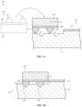
- FIGS. 1 A- 1 Bdepict a simplified cross-section diagram of an operation of aligning two photonic circuit chips by leveraging complementary geometry, such as described herein.
- FIG. 1 Adepicts a diagram of a portion of a photonic integrated circuit 100 that is defined at least in part by two chips that can be assembled and intercoupled by leveraging a flip-chip technique, as described herein.
- a first chip 102can serve as a base substrate over which a second chip 104 can be positioned.
- the first chip 102 and the second chip 104can each include different photonic circuit elements that may require precise multi-axis alignment. More specifically, the photonic circuit elements of each chip may require precise alignment along an X axis (e.g., from right to left of FIG. 1 A ), along a Y axis (e.g., into or out of FIG. 1 A ), and along a Z axis (e.g., from top to bottom of FIG. 1 A ). In this example, the X and Y axes can define a surface plane of the first chip 102 and the Z axis can extend through a thickness of the first chip 102 . Misalignment of the two photonic circuit elements may result in substantial optical power loss and/or low coupling efficiency which, in turn, can affect and degrade performance of the photonic integrated circuit 100 .
- the first chip 102 and the second chip 104each are formed with complementary geometry that, when mutually engaged, precisely aligns the first chip 102 with the second chip 104 .
- the second chip 104can include a light source intended to be optically coupled to a waveguide defined on or through the first chip 102 .
- a light sourceintended to be optically coupled to a waveguide defined on or through the first chip 102 .
- either chipcan include one or more passive or active optical elements or photonic elements or semiconductor circuit elements that, in turn may be configured to align with a corresponding optical coupling or conductive coupling of the other chip.
- the embodiments that followreference intercoupled chips that include a single photonic circuit element coupling to a single photonic circuit element, but it may be appreciated that this is merely one example, and that other architectures and implementations can leverage embodiments described herein.
- the second chip 104includes a base substrate 106 over which at least a portion of a photonic integrated circuit element 108 may be formed (e.g., a light source).
- a photonic integrated circuit element 108may be formed (e.g., a light source).
- the base substrate 106is formed form silicon (e.g., bulk silicon) although this may not be required of all embodiments.
- the second chip 104can also define at least two protrusions, identified as the protrusions 110 and 112 .
- the protrusions 110 and 112are show as extending from a surface of the photonic integrated element 108 , but this may not be required of all embodiments.
- the protrusions 110 , 112can be formed from a surface of the base substrate 106 .
- one or more protrusions and/or one or more channelsmay be formed on, disposed on, or otherwise formed from the same base substrate of the same chip. More specifically, a single chip can include both protrusions and channels configured to mate with corresponding protrusions and channels of another chip.
- the protrusions 110 , 112are shown with identical cross-sectional profiles, but this may not be required of all embodiments.
- the protrusion 110may be shorter along the Z-axis than the protrusion 112 , the protrusion 110 may be deeper along the Z-axis than the protrusion 112 .
- the protrusion 110may have a circular cross section/profile, whereas the protrusion 112 may have a triangular or otherwise polygonal cross section.
- a person of skill in the artmay readily appreciate that any suitable arrangement and geometry of the protrusions 110 , 112 may be used.
- the first chip 102can include a base substrate 114 .
- the base substrate 114may be formed from silicon, although this is not required of all embodiments.
- the base substrate 114can have formed (or disposed, placed, and so on) thereon at least a portion of a photonic circuit element 116 (e.g., a waveguide).
- the photonic circuit element 116may be configured to precisely align with the photonic circuit element 108 when the second chip 104 is positioned over and aligned with the first chip 102 . More specifically, an optical axis (light emitting axis, input facet, output facet, and so on) of the photonic circuit element 116 may be configured to precisely align with the photonic circuit element 108 .
- the photonic circuit element 116may be a first waveguide and the second photonic circuit element 108 may be a second waveguide.
- the base substrate 114includes at least two channels, identified as the channels 118 and 120 .
- the channels 118 and 120are show as extending from a surface of the base substrate 114 , but this may not be required of all embodiments.
- the protrusions 110 , 112can be formed from a surface of the photonic integrated circuit element 116 .
- the channels 118 , 120 and the protrusions 110 , 112can be formed with complementary geometry such that when the second chip 104 is positioned over the first chip 102 , and the second chip 104 is advanced in the XY plane, the protrusions 110 , 112 can become engaged with the channels 118 , 120 and the triangular geometry of the channels 118 , 120 can guide the protrusion 110 , 112 to a specific Z position, thereby precisely aligning the photonic circuit element 116 and the photonic circuit element 108 .
- the dual alignment channel geometry illustrated in FIGS. 1 A and 1 Bprovides for alignment along all three primary axes, namely the X-axis, the Y-axis and the Z-axis.
- FIGS. 1 A- 1 BThese foregoing embodiments depicted in FIGS. 1 A- 1 B and the various alternatives thereof and variations thereto are presented, generally, for purposes of explanation, and to facilitate an understanding of various configurations and constructions of a method of aligning two chips to form a photonic integrated circuit, such as described herein. However, it will be apparent to one skilled in the art that some of the specific details presented herein may not be required in order to practice a particular described embodiment, or an equivalent thereof.
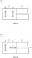
- FIGS. 2 A- 2 Ddepict example views of a chip as described herein that can be formed with a set of surface features that may be leveraged with complementary geometry of corresponding surface features of a second chip to precisely align with that chip, such as described herein.
- FIG. 2 Adepicts a view of a chip 200 that includes a base layer 202 onto which one or more features can be formed that, in turn, can define at least a portion of a photonic integrated circuit, such as described herein.
- the chipcan include an elevated portion 204 that supports a waveguide 206 that can define an input/output edge facet configured to optically and/or mechanically couple to an input/output edge facet of another waveguide formed/defined on a separate substrate.
- Adjacent to or otherwise separated from the elevated portion 204can be defined two or more surface features, identified as the surface feature 208 and the surface feature 210 .
- the surface feature 208 and/or the surface feature 210can be formed into or out of an upper surface of the base layer 202 . More generally, the surface feature 208 and/or the surface feature 210 may be embossed features or debossed features; the surface feature 208 and/or the surface feature 210 may define one or more channels or may define one or more protrusions.
- the surface feature 208 and/or the surface feature 210can exhibit any suitable cross-sectional profile or geometry.
- the surface feature 208 and/or the surface feature 210each have a triangular cross-sectional profile that may be formed via photolithographically-masked directional etch or anisotropic etch processes. This is merely one example cross-sectional profile; in other examples, a surface feature as described herein can be formed to have any suitable shape.
- the surface feature 208 and the surface feature 210have a generally rectilinear shape, and are arranged in parallel to one another. This is not required of all embodiments, for example in FIG. 2 B , the surface feature 210 may be oriented at an angle perpendicular to the surface feature 210 .
- the surface feature 208 and the surface feature 210are shown as the only two surface features defined onto the chip 200 ; this is not required of all embodiments.
- more than two surface featurescan be defined.
- a third surface feature 212is defined between the surface feature 208 and the surface feature 210 .
- each surface feature—whether embossed or debossed from a surface or layer of the chip 200is shown as having the same size and cross-sectional profile. This is not required of all embodiments.
- the surface feature 208 and the surface feature 210may have different sizes and/or may be arranged at an oblique angle relative to one another.
- the surface feature 210is depicted has larger than the surface feature 208 , which in turn is oriented at a non-parallel, non-perpendicular, oblique angle relative to the surface feature 210 .
- FIGS. 2 A- 2 Dillustrate example possible geometries of surface features that may be formed into a chip, such as the first chip 102 or the second chip 104 of FIGS. 1 A- 1 B . More generally, for these embodiments show in FIGS. 2 A- 2 D , it may be appreciated that a similar pattern to that which is shown can be formed into a second chip or chip in order that the chip 200 can be coupled to and precisely aligned with the other chip.
- FIGS. 2 A- 2 DThese foregoing embodiments depicted in FIGS. 2 A- 2 D and the various alternatives thereof and variations thereto are presented, generally, for purposes of explanation, and to facilitate an understanding of various configurations and constructions of a method of defining and/or positioning surface features onto a chip for aligning that chip with another chip having complementary geometry to form a photonic integrated circuit, such as described herein.
- a method of defining and/or positioning surface features onto a chip for aligning that chip with another chip having complementary geometry to form a photonic integrated circuitsuch as described herein.
- some of the specific details presented hereinmay not be required in order to practice a particular described embodiment, or an equivalent thereof.
- a surface feature extending proud of a surface configured to mate with and/or interface with a surface feature defining a channelmay have different cross-sectional profiles.
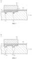
- FIG. 3depicts a simplified cross-section diagram of a pair of photonic circuit chips aligned by leveraging complementary geometry, such as described herein.
- a photonic integrated circuit 300can be formed by mating a first chip 302 with a second chip 304 .
- the first chipincludes a first circuit element 306 (e.g., waveguide, light source, splitter, delay line, Bragg reflector, other reflectors, mode field converters, and so on) may be aligned with a second circuit element 308 of the second chip 304 when surface features of the first and second chips are engaged.
- a first circuit element 306e.g., waveguide, light source, splitter, delay line, Bragg reflector, other reflectors, mode field converters, and so on
- the first chip 302includes a surface feature 310 and a surface feature 312 , each having a rectangular cross-section.
- the second chip 304includes a surface feature 314 and a surface feature 316 , each having a triangular cross-section.
- the surface feature 310may be configured to mate with and/or engage with the surface feature 314 and the surface feature 312 may be configured to mate with and/or engage with the surface feature 316 .
- protrusionscan have a triangular cross-sectional profile and channels, as described herein, can have a different cross-sectional profile.
- FIG. 4depicts another simplified cross-section diagram of a pair of photonic circuit chips aligned by leveraging complementary geometry, such as described herein.
- a photonic integrated circuit 400can be formed by mating a first chip 402 with a second chip 404 .
- the first chipincludes a first circuit element 406 that may be aligned with a second circuit element 408 of the second chip 404 when surface features of the first and second chips are engaged.
- the first chip 402includes a surface feature 410 and a surface feature 412 , each having a triangular cross-section.
- the second chip 404includes a surface feature 414 and a surface feature 416 , each having a rectangular cross-section.
- the surface feature 410may be configured to mate with and/or engage with the surface feature 414 and the surface feature 412 may be configured to mate with and/or engage with the surface feature 416 .
- FIG. 5depicts a simplified cross-section diagram of a pair of photonic circuit chips aligned by leveraging complementary geometry, such as described herein.
- a photonic integrated circuit 500can be formed by mating and conductively coupling a first chip 502 with a second chip 504 .
- the first chip 502includes a surface feature 506 which may be a solder ball or other conductive surface.
- the first chipmay also include a surface feature 508 , which may also be a solder ball or other conductive surface.
- Each of the surface features 506 , 508can have a circular or curved cross-section, but this is not required of all embodiments.
- the second chip 504includes a surface feature 512 and a surface feature 514 , each having a triangular cross-section.
- the surface feature 508may be configured to mate with and/or engage with the surface feature 512 and the surface feature 506 may be configured to mate with and/or engage with the surface feature 514 .
- the conductive surface features of each chip(which can extend into the surface features 512 , 514 ) can form a conductive coupling between the chips, electrically coupling semiconductor circuitry defined thereon or therein.
- the surface featuresmay provide for precise alignment of photonic integrated circuit elements, such as an element 516 of the first chip and an element 518 of the second chip.
- FIGS. 2 A- 5These foregoing embodiments depicted in FIGS. 2 A- 5 and the various alternatives thereof and variations thereto are presented, generally, for purposes of explanation, and to facilitate an understanding of various configurations and constructions of a method of defining and/or positioning surface features onto a chip for aligning that chip with another chip having complementary geometry to form a photonic integrated circuit, such as described herein.
- a method of defining and/or positioning surface features onto a chip for aligning that chip with another chip having complementary geometry to form a photonic integrated circuitsuch as described herein.
- some of the specific details presented hereinmay not be required in order to practice a particular described embodiment, or an equivalent thereof.
- photonic circuit elements formed on different chipscan be aligned and/or mechanically, optically, and/or electrically coupled to one another.
- complementary geometry defined in part by photonic circuit element manufacturing operationscan be defined in any number of suitable ways.
- different channels and corresponding protrusionscan intersect.
- channels and protrusionscan be disposed parallel to one another and perpendicular to an optical axis of a photonic component of one phonic integrated circuit defined on a chip.
- a single chipcan include at least one channel feature and at least one protruding feature.
- a channelcan have a tapering geometry to encourage particular alignment by sliding a protruding feature into the tapering channel.
- optical components formed onto, into, or otherwise disposed on each respective chipcan be aligned so as to share a common optical axis.
- channelsmay have keyed depth so that optical alignment will only be achieved if particular protrusions are aligned with particular channels.
- an alignment structure as described hereincan be used to align both a semiconductor circuit and a photonic circuit, each formed onto and/or defined onto respective chips.
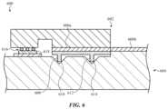
- FIG. 6depicts another simplified cross-section diagram of a pair of photonic circuit chips aligned by leveraging complementary geometry, such as described herein.
- a photonic integrated circuit 600includes a first chip 602 disposed over a second chip 604 .
- the first chip 602 and the second chip 604are aligned in part by complementary geometry, as described herein. More specifically, a photonic circuit element 606 a of the first chip 602 can be aligned with a second photonic circuit element 606 b of the second chip 604 .
- the alignmentcan be effected by mating and/or engagement of surface features of the first chip 602 and the second chip 604 .
- the first chip 602can include a protrusion 608 that mates with a channel 610 of the second chip 604 .
- the first chip 602can include a second protrusion 614 that mates with a channel 612 of the second chip 604 .
- the first chip 602 and the second chip 604can be conductively coupled in one or more suitable locations to conductively intercouple silicon circuitry, either digital or analog, of the respective chips.
- solder balls 616can conductively couple conductive pads or traces of the first chip 602 with a circuit or circuit element 618 of the second chip 604 . More specifically the solder balls 616 can facilitate one or more electrical connections between the first chip 602 and the second chip 604 ; in some cases, the solder balls may be reflowed or otherwise melted in a manufacturing step in order to conductively and mechanically couple the first and second chips to one another.
- circuit element 618can be configured to emit light or receive light, for example.
- FIGS. 2 A- 6These foregoing embodiments depicted in FIGS. 2 A- 6 and the various alternatives thereof and variations thereto are presented, generally, for purposes of explanation, and to facilitate an understanding of various configurations and constructions of a method of defining and/or positioning surface features onto a chip for aligning that chip with another chip having complementary geometry to form a photonic integrated circuit, such as described herein.
- a method of defining and/or positioning surface features onto a chip for aligning that chip with another chip having complementary geometry to form a photonic integrated circuitsuch as described herein.
- some of the specific details presented hereinmay not be required in order to practice a particular described embodiment, or an equivalent thereof.
- any structure as shown in these figures and/or described hereincan be formed onto any suitable base substrate.
- at least one of the chipsmay be flipped and/or otherwise positioned onto a second chip, after which an alignment between the two chips may be guided through three dimensions.
- a channel as described hereinmay be both embossed and debossed.
- regions around a channelcan be etched away such that the channel is defined at least in part by sidewalls that extend proud of a substrate surface.
- FIG. 7 Adepicts a first stage of defining a bonded flip-chip structure, as described herein.
- a set of separately manufactured chips 700may include a first chip 702 and a second chip 704 .
- the first chipas with other embodiments described herein can include a first surface feature 706 and a second surface feature 708 , each of which extend from a surface of the first chip 702 .
- the second chip 704can include a first surface feature 710 and a second surface feature 712 that are respectively configured to mate with and engage with the first surface feature 706 and the second surface feature 708 .
- the first chip 702can be flipped/inverted onto the second chip 704 so as to effect precise alignment (lateral and vertical) between a first photonic circuit element 716 defined on the first chip 702 and a second photonic circuit element 718 defined on the second chip 704 , such as shown in FIG. 7 B .
- the first chip 704may be mechanically guided (e.g., via pick and place machine, manually, by vibration, and so on) such that the respective surface feature of each chip are engaged, such as shown in FIG. 7 C .
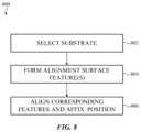
- FIG. 8is a flowchart depicting example operations of a method of aligning chips, such as described herein.
- the method 800includes operation 802 at which a chip is selected. Thereafter, at operation 804 , two or more alignment features can be formed into or onto the chip. Finally, at operation 806 , the chip can be aligned with corresponding features of another chip, and the two chips can be affixed to one another in a suitable manner.
- the phrase “at least one of” preceding a series of items, with the term “and” or “or” to separate any of the items,modifies the list as a whole, rather than each member of the list.
- the phrase “at least one of”does not require selection of at least one of each item listed; rather, the phrase allows a meaning that includes at a minimum one of any of the items, and/or at a minimum one of any combination of the items, and/or at a minimum one of each of the items.
- the phrases “at least one of A, B, and C” or “at least one of A, B, or C”each refer to only A, only B, or only C; any combination of A, B, and C; and/or one or more of each of A, B, and C.
- an order of elements presented for a conjunctive or disjunctive list provided hereinshould not be construed as limiting the disclosure to only that order provided.
Landscapes
- Physics & Mathematics (AREA)
- General Physics & Mathematics (AREA)
- Optics & Photonics (AREA)
- Optical Integrated Circuits (AREA)
Abstract
Description
Claims (15)
Priority Applications (1)
| Application Number | Priority Date | Filing Date | Title |
|---|---|---|---|
| US17/850,828US12204155B2 (en) | 2021-09-24 | 2022-06-27 | Chip-to-chip optical coupling for photonic integrated circuits |
Applications Claiming Priority (2)
| Application Number | Priority Date | Filing Date | Title |
|---|---|---|---|
| US202163247992P | 2021-09-24 | 2021-09-24 | |
| US17/850,828US12204155B2 (en) | 2021-09-24 | 2022-06-27 | Chip-to-chip optical coupling for photonic integrated circuits |
Publications (2)
| Publication Number | Publication Date |
|---|---|
| US20230102967A1 US20230102967A1 (en) | 2023-03-30 |
| US12204155B2true US12204155B2 (en) | 2025-01-21 |
Family
ID=85706031
Family Applications (1)
| Application Number | Title | Priority Date | Filing Date |
|---|---|---|---|
| US17/850,828ActiveUS12204155B2 (en) | 2021-09-24 | 2022-06-27 | Chip-to-chip optical coupling for photonic integrated circuits |
Country Status (1)
| Country | Link |
|---|---|
| US (1) | US12204155B2 (en) |
Families Citing this family (1)
| Publication number | Priority date | Publication date | Assignee | Title |
|---|---|---|---|---|
| CN111323878B (en)* | 2020-04-01 | 2021-10-15 | 联合微电子中心有限责任公司 | Coupling alignment device and method for laser chip and silicon-based optoelectronic chip |
Citations (205)
| Publication number | Priority date | Publication date | Assignee | Title |
|---|---|---|---|---|
| US4227091A (en) | 1978-02-27 | 1980-10-07 | Erwin Sick Gmbh, Optik-Elektronik | Optical monitoring apparatus |
| US4318058A (en) | 1979-04-24 | 1982-03-02 | Nippon Electric Co., Ltd. | Semiconductor diode laser array |
| EP0203810A2 (en) | 1985-05-31 | 1986-12-03 | Xerox Corporation | Semiconductor lasers |
| US4880304A (en) | 1987-04-01 | 1989-11-14 | Nippon Colin Co., Ltd. | Optical sensor for pulse oximeter |
| US4896325A (en) | 1988-08-23 | 1990-01-23 | The Regents Of The University Of California | Multi-section tunable laser with differing multi-element mirrors |
| JPH04116878A (en) | 1990-09-07 | 1992-04-17 | Ricoh Co Ltd | Semiconductor laser element with heater |
| US5140605A (en) | 1991-06-27 | 1992-08-18 | Xerox Corporation | Thermally stabilized diode laser structure |
| US5159700A (en)* | 1984-01-16 | 1992-10-27 | Texas Instruments Incorporated | Substrate with optical communication systems between chips mounted thereon and monolithic integration of optical I/O on silicon substrates |
| US5287376A (en) | 1992-12-14 | 1994-02-15 | Xerox Corporation | Independently addressable semiconductor diode lasers with integral lowloss passive waveguides |
| US5319725A (en)* | 1991-12-23 | 1994-06-07 | International Business Machines Corporation | Bilithic composite for optoelectronic integration |
| US5325392A (en) | 1992-03-06 | 1994-06-28 | Nippon Telegraph And Telephone Corporation | Distributed reflector and wavelength-tunable semiconductor laser |
| US5341391A (en) | 1992-05-11 | 1994-08-23 | Mitsubishi Denki Kabushiki Kaisha | Variable wavelength semiconductor laser |
| US5384797A (en) | 1992-09-21 | 1995-01-24 | Sdl, Inc. | Monolithic multi-wavelength laser diode array |
| US5483261A (en) | 1992-02-14 | 1996-01-09 | Itu Research, Inc. | Graphical input controller and method with rear screen image detection |
| US5488204A (en) | 1992-06-08 | 1996-01-30 | Synaptics, Incorporated | Paintbrush stylus for capacitive touch sensor pad |
| WO1996011416A1 (en) | 1994-10-10 | 1996-04-18 | France Telecom | Optical filter for a plurality of guided wavelengths |
| US5515391A (en) | 1994-03-07 | 1996-05-07 | Sdl, Inc. | Thermally balanced diode laser package |
| US5574561A (en)* | 1994-12-22 | 1996-11-12 | The Whitaker Corporation | Kinematic mounting of optical and optoelectronic elements on silicon waferboard |
| US5695520A (en) | 1995-12-05 | 1997-12-09 | Bruckner; James V. | Pressure-applying device having plate-supported pressure-applying body secured to flexible band |
| US5708674A (en) | 1995-01-03 | 1998-01-13 | Xerox Corporation | Semiconductor laser or array formed by layer intermixing |
| CN1173226A (en) | 1994-12-19 | 1998-02-11 | 加利福尼亚大学 | A Pulse Radar with Scan Interval Gate |
| US5742631A (en) | 1996-07-26 | 1998-04-21 | Xerox Corporation | Independently-addressable monolithic laser arrays |
| US5780875A (en) | 1995-08-30 | 1998-07-14 | Hitachi, Ltd. | Hybrid optical integration assembly using optical platform |
| US5825352A (en) | 1996-01-04 | 1998-10-20 | Logitech, Inc. | Multiple fingers contact sensing method for emulating mouse buttons and mouse operations on a touch sensor pad |
| US5835079A (en) | 1996-06-13 | 1998-11-10 | International Business Machines Corporation | Virtual pointing device for touchscreens |
| US5850411A (en) | 1996-09-17 | 1998-12-15 | Sdl, Inc | Transverse electric (TE) polarization mode AlGaInP/GaAs red laser diodes, especially with self-pulsating operation |
| US5880411A (en) | 1992-06-08 | 1999-03-09 | Synaptics, Incorporated | Object position detector with edge motion feature and gesture recognition |
| US5898806A (en)* | 1991-11-07 | 1999-04-27 | Nec Corporation | Optical interconnection circuit structure |
| US5915165A (en) | 1997-12-15 | 1999-06-22 | Xerox Corporation | Method of manufacturing vertical cavity surface emitting semiconductor lasers using intermixing and oxidation |
| US6043104A (en) | 1996-08-28 | 2000-03-28 | Canon Kabushiki Kaisha | Fabrication method of a polarization selective semiconductor laser |
| JP2000163031A (en) | 1998-11-25 | 2000-06-16 | Seiko Epson Corp | Portable information devices and information storage media |
| US6160936A (en)* | 1997-01-19 | 2000-12-12 | Samsung Electronics Co., Ltd. | Apparatus and method for combining optical waveguide and optical fiber |
| US6188391B1 (en) | 1998-07-09 | 2001-02-13 | Synaptics, Inc. | Two-layer capacitive touchpad and method of making same |
| US6250819B1 (en)* | 1999-04-28 | 2001-06-26 | Highwave Optical Technologies | Mounting of an integrated optic circuit on a motherboard for the connection of optic fibers to form a miniature optical component |
| US6263222B1 (en) | 1991-03-07 | 2001-07-17 | Masimo Corporation | Signal processing apparatus |
| US20010010743A1 (en)* | 2000-02-02 | 2001-08-02 | Ian Cayrefourcq | Passive alignment using slanted wall pedestal |
| US6310610B1 (en) | 1997-12-04 | 2001-10-30 | Nortel Networks Limited | Intelligent touch display |
| US6323846B1 (en) | 1998-01-26 | 2001-11-27 | University Of Delaware | Method and apparatus for integrating manual input |
| US20010055447A1 (en)* | 2000-06-21 | 2001-12-27 | Daniel Delprat | Hybrid alignment using calibrated substrates |
| US6341116B1 (en) | 1999-04-13 | 2002-01-22 | Industrial Technology Research Institute | Compact optical pick-up head employing non-diffractive element |
| US6345135B1 (en) | 1998-05-06 | 2002-02-05 | Douglas Charles John Reid | Multi-wavelength optical reflector |
| US6373872B2 (en) | 1999-10-19 | 2002-04-16 | Sparkolor Corporation | Channel-switched tunable laser for DWDM communications |
| US6393185B1 (en) | 1999-11-03 | 2002-05-21 | Sparkolor Corporation | Differential waveguide pair |
| US6475153B1 (en) | 2000-05-10 | 2002-11-05 | Motorola Inc. | Method for obtaining blood pressure data from optical sensor |
| JP2002342033A (en) | 2001-05-21 | 2002-11-29 | Sony Corp | Non-contact type user input device |
| US20020181521A1 (en) | 2000-05-04 | 2002-12-05 | Crowder Paul F. | Gain voltage control of sampled grating distributed bragg reflector lasers |
| US6516017B1 (en) | 1999-11-11 | 2003-02-04 | Mitsubishi Denki Kabushiki Kaisha | Multiwavelength semiconductor laser device with single modulator and drive method therefor |
| GB2380058A (en) | 2001-09-21 | 2003-03-26 | Marconi Caswell Ltd | Telecommunication laser transmitter systems and methods of operating such systems |
| US6558335B1 (en) | 2000-11-22 | 2003-05-06 | Medwave, Inc | Wrist-mounted blood pressure measurement device |
| CN1416533A (en) | 2000-02-07 | 2003-05-07 | 格拉斯哥大学理事会 | Improved integrated optical device |
| US6605045B2 (en) | 2000-06-14 | 2003-08-12 | Denso Corporation | Wristwatch-type human pulse wave sensor attached on back side of user's wrist |
| US6628686B1 (en) | 2001-11-16 | 2003-09-30 | Fox-Tek, Inc | Integrated multi-wavelength and wideband lasers |
| US6647032B1 (en) | 2002-01-31 | 2003-11-11 | Intel Corporation | Thermally wavelength tunable laser having selectively activated gratings |
| US6661955B1 (en)* | 2002-02-04 | 2003-12-09 | Siwave, Inc. | Kinematic and non-kinematic passive alignment assemblies and methods of making the same |
| US6690693B1 (en) | 2000-05-04 | 2004-02-10 | Agility Communications, Inc. | Power and wavelength control of sampled grating distributed Bragg reflector lasers |
| US6690387B2 (en) | 2001-12-28 | 2004-02-10 | Koninklijke Philips Electronics N.V. | Touch-screen image scrolling system and method |
| US6699199B2 (en) | 2000-04-18 | 2004-03-02 | Massachusetts Institute Of Technology | Photoplethysmograph signal-to-noise line enhancement |
| CN1488183A (en) | 2001-01-23 | 2004-04-07 | ����˹���ѧ���»� | Improvements in semiconductor lasers or related aspects |
| US20040126117A1 (en) | 2002-12-18 | 2004-07-01 | Tdk Corporation | Optical module and a method of fabricating the same |
| US6788719B2 (en) | 2000-05-04 | 2004-09-07 | Agility Communications, Inc. | Open loop control of SGDBR lasers |
| US20040174915A1 (en) | 2002-09-18 | 2004-09-09 | Adc Telecommunications, Inc. | Method for characterizing tunable lasers |
| US6795453B2 (en) | 2000-10-30 | 2004-09-21 | Santur Corporation | Laser thermal tuning |
| US6803604B2 (en) | 2001-03-13 | 2004-10-12 | Ricoh Company, Ltd. | Semiconductor optical modulator, an optical amplifier and an integrated semiconductor light-emitting device |
| US6807206B2 (en) | 2001-04-16 | 2004-10-19 | The Furukawa Electric Co., Ltd. | Semiconductor laser device and drive control method for a semiconductor laser device |
| US6816529B2 (en) | 2001-03-30 | 2004-11-09 | Santur Corporation | High speed modulation of arrayed lasers |
| US6829400B2 (en) | 2001-03-26 | 2004-12-07 | Olympus Corporation | Optical path switching apparatus |
| US20040255318A1 (en) | 1999-05-20 | 2004-12-16 | Braitberg Michael F. | Cartridge containing first-surface storage medium |
| US20050127383A1 (en) | 2003-12-10 | 2005-06-16 | Takeshi Kikawa | Laser diode and manufacturing method thereof |
| US6911629B2 (en) | 2002-03-16 | 2005-06-28 | Agilent Technologies, Inc. | Method and system for turning on an optical radiation source |
| JP2005175021A (en) | 2003-12-08 | 2005-06-30 | Nippon Telegr & Teleph Corp <Ntt> | Tunable light source and optical transmitter |
| US6915955B2 (en) | 1996-01-02 | 2005-07-12 | Jjl Technologies Llc | Apparatus for determining multi-bit data via light received by a light receiver and coupled to spectral sensors that measure light in spectral bands |
| US20050169327A1 (en) | 1998-10-20 | 2005-08-04 | Quantum Devices, Inc. | Method and apparatus reducing electrical and thermal crosstalk of a laser array |
| WO2005091036A1 (en) | 2004-03-19 | 2005-09-29 | Nec Corporation | Optical module and method for manufacturing the same |
| CN1703783A (en) | 2002-04-10 | 2005-11-30 | 英坦斯有限公司 | Integrated active photonic device and photoelectric detector |
| US6987906B2 (en) | 2002-08-27 | 2006-01-17 | Nippon Sheet Glass Co., Ltd. | Optical connection device |
| US6990129B2 (en) | 2000-08-07 | 2006-01-24 | Xlight Photonics Inc. | Characterization of multiple section semiconductor lasers |
| US7015894B2 (en) | 2001-09-28 | 2006-03-21 | Ricoh Company, Ltd. | Information input and output system, method, storage medium, and carrier wave |
| US20060088068A1 (en) | 2004-10-13 | 2006-04-27 | Intune Technologies | Low noise swept wavelength laser system and method |
| US7106778B2 (en) | 2001-03-19 | 2006-09-12 | Bookham Technology, Plc | Tuneable laser |
| US7130325B2 (en) | 2003-05-02 | 2006-10-31 | Electronics And Telecommunications Research Institute | Sampled grating distributed feedback wavelength tunable semiconductor laser integrated with sampled grating distributed Bragg reflector |
| EP1753104A2 (en) | 2005-08-11 | 2007-02-14 | Eudyna Devices Inc. | Semiconductor laser |
| US7189011B2 (en) | 2002-09-25 | 2007-03-13 | Avago Technologies General Ip (Singapore) Pte. Ltd. | Optoelectronic assembly |
| US7196355B2 (en) | 2003-03-07 | 2007-03-27 | Avanex Corporation | Integrated thermal sensor for optoelectronic modules |
| US20070116076A1 (en) | 2005-11-21 | 2007-05-24 | Frank Wang | Controlling optical power and extincation ratio of a semiconductor laser |
| US20070223549A1 (en) | 2006-03-23 | 2007-09-27 | Nl Nanosemiconductor Gmbh | High-Power Optoelectronic Device with Improved Beam Quality Incorporating A Lateral Mode Filtering Section |
| US7283242B2 (en) | 2003-04-11 | 2007-10-16 | Thornton Robert L | Optical spectroscopy apparatus and method for measurement of analyte concentrations or other such species in a specimen employing a semiconductor laser-pumped, small-cavity fiber laser |
| US20080063016A1 (en) | 2006-09-13 | 2008-03-13 | Vikram Bhatia | Thermal compensation in semiconductor lasers |
| US7394734B2 (en) | 2005-05-24 | 2008-07-01 | Sony Corporation | Optical disk drive using near-field light, optical disk apparatus, and method for driving the apparatus |
| JP2008262116A (en) | 2007-04-13 | 2008-10-30 | Nippon Telegr & Teleph Corp <Ntt> | Optical waveguide circuit and manufacturing method thereof |
| US20080310470A1 (en) | 2007-06-18 | 2008-12-18 | Lehigh University | Broadband semiconductor laser |
| US7468637B2 (en) | 2006-04-19 | 2008-12-23 | Sarnoff Corporation | Batch-fabricated, RF-interrogated, end transition, chip-scale atomic clock |
| US7469092B2 (en) | 2003-03-31 | 2008-12-23 | Zolo Technologies, Inc. | Method and apparatus for the monitoring and control of a process |
| US7480317B2 (en) | 2006-09-26 | 2009-01-20 | Corning Incorporated | Thermal compensation in semiconductor lasers |
| US7483453B2 (en) | 2002-12-20 | 2009-01-27 | Intune Technologies Limited | Frequency setting of a multisection laser diode taking into account thermal effects |
| US7526007B2 (en) | 2005-12-15 | 2009-04-28 | Palo Alto Research Center Incorporated | Buried lateral index guided lasers and lasers with lateral current blocking layers |
| DE102008014093A1 (en) | 2007-12-27 | 2009-07-02 | Osram Opto Semiconductors Gmbh | Edge-emitting semiconductor laser chip with at least one current barrier |
| US7558301B2 (en) | 2006-12-20 | 2009-07-07 | Industrial Technology Research Institute | Multiwavelength semiconductor laser array and method of fabricating the same |
| EP2091118A1 (en) | 2006-10-31 | 2009-08-19 | Anritsu Corporation | Semiconductor optical device, semiconductor laser using the semiconductor optical device, and optical transponder using the semiconductor laser |
| US7616110B2 (en) | 2005-03-11 | 2009-11-10 | Aframe Digital, Inc. | Mobile wireless customizable health and condition monitor |
| US7620078B2 (en) | 2005-03-17 | 2009-11-17 | Anritsu Corporation | Tunable semiconductor laser device, manufacturing method therefor, and gas detector using therewith |
| EP2120301A1 (en) | 2007-03-08 | 2009-11-18 | Nippon Telegraph and Telephone Corporation | Wavelength variable semiconductor laser element, and apparatus and method for controlling the same |
| US7663607B2 (en) | 2004-05-06 | 2010-02-16 | Apple Inc. | Multipoint touchscreen |
| US7664156B2 (en) | 2005-03-03 | 2010-02-16 | Nec Corporation | Wavelength tunable laser |
| US20100046562A1 (en) | 2006-09-20 | 2010-02-25 | The Provost, Fellows And Scholars Of The College Of The Holy And Undivided Trinity Of Queen Elizabe | Tunable laser device and a method for producing light of respective selectable wavelengths |
| US7701985B2 (en) | 2007-11-09 | 2010-04-20 | Lightwire, Inc. | SOI-based tunable laser |
| US7738935B1 (en) | 2002-07-09 | 2010-06-15 | Pacesetter, Inc. | Methods and devices for reduction of motion-induced noise in pulse oximetry |
| US7751658B2 (en) | 2001-10-09 | 2010-07-06 | Infinera Corporation | Monolithic transmitter photonic integrated circuit (TxPIC) having tunable modulated sources with feedback system for source power level or wavelength tuning |
| US7852898B2 (en) | 2007-09-28 | 2010-12-14 | Panasonic Corporation | Semiconductor laser device and method for manufacturing the same |
| US7885302B2 (en) | 2007-02-28 | 2011-02-08 | Osram Opto Semiconductors Gmbh | Integrated tapered diode laser arrangement and method for producing it |
| US7903704B2 (en) | 2006-06-23 | 2011-03-08 | Pranalytica, Inc. | Tunable quantum cascade lasers and photoacoustic detection of trace gases, TNT, TATP and precursors acetone and hydrogen peroxide |
| US8000368B2 (en) | 2006-07-26 | 2011-08-16 | Santur Corporation | Modulated semiconductor DFB laser array with a MEMS-based RF switch |
| DE102010020625A1 (en) | 2010-05-14 | 2011-11-17 | Osram Opto Semiconductors Gmbh | Edge-emitting semiconductor laser |
| US8121169B2 (en) | 2009-04-14 | 2012-02-21 | Corning Incorporated | Split control of front and rear DBR grating portions |
| CN102522697A (en) | 2012-01-09 | 2012-06-27 | 桂林优西科学仪器有限责任公司 | Distributed Bragg reflector (DBR) tunable laser source system and control method thereof |
| US8222084B2 (en) | 2010-12-08 | 2012-07-17 | Skorpios Technologies, Inc. | Method and system for template assisted wafer bonding |
| US8259770B2 (en) | 2009-10-11 | 2012-09-04 | Hewlett-Packard Indigo B.V. | Laser array |
| US8279441B2 (en) | 2007-04-03 | 2012-10-02 | Mutoh Industries Ltd. | Spectrophotometer and method |
| US8320763B2 (en) | 2006-12-05 | 2012-11-27 | Electronics And Telecommunications Research Institute | Planar lightwave circuit (PLC) device wavelength tunable light source comprising the same device and wavelength division multiplexing-passive optical network (WDM-PON) using the same light source |
| US8352008B2 (en) | 2009-06-10 | 2013-01-08 | Medtronic, Inc. | Active noise cancellation in an optical sensor signal |
| US8378811B2 (en) | 2005-03-11 | 2013-02-19 | Aframe Digital, Inc. | Mobile wireless customizable health and condition monitor |
| US8405699B2 (en) | 2009-03-11 | 2013-03-26 | Sony Corporation | Light stabilizer, light stabilization method, and printer |
| US8437825B2 (en) | 2008-07-03 | 2013-05-07 | Cercacor Laboratories, Inc. | Contoured protrusion for improving spectroscopic measurement of blood constituents |
| US8442608B2 (en) | 2007-12-28 | 2013-05-14 | Covidien Lp | System and method for estimating physiological parameters by deconvolving artifacts |
| US8457172B2 (en) | 2005-09-29 | 2013-06-04 | Oclaro Technology Limited | Bragg grating structure |
| US8479122B2 (en) | 2004-07-30 | 2013-07-02 | Apple Inc. | Gestures for touch sensitive input devices |
| US20130292571A1 (en) | 2011-06-02 | 2013-11-07 | Infrasign, Inc. | Optically multiplexed mid-infrared laser systems and uses thereof |
| US8618930B2 (en) | 2005-03-11 | 2013-12-31 | Aframe Digital, Inc. | Mobile wireless customizable health and condition monitor |
| US8649839B2 (en) | 1996-10-10 | 2014-02-11 | Covidien Lp | Motion compatible sensor for non-invasive optical blood analysis |
| US8750341B2 (en) | 2008-01-04 | 2014-06-10 | Mindspeed Technologies, Inc. | Method and apparatus for reducing optical signal speckle |
| US8774243B2 (en) | 2010-08-31 | 2014-07-08 | Electronics And Telecommunications Research Institute | Dual mode semiconductor laser and terahertz wave apparatus using the same |
| US8781548B2 (en) | 2009-03-31 | 2014-07-15 | Covidien Lp | Medical sensor with flexible components and technique for using the same |
| US8805129B2 (en)* | 2009-10-13 | 2014-08-12 | Electronics And Telecommunications Research Institute | Optical devices and methods of fabricating the same |
| US8886465B2 (en) | 2007-02-28 | 2014-11-11 | Medtronic, Inc. | Implantable tissue perfusion sensing system and method |
| CN104303038A (en) | 2012-05-16 | 2015-01-21 | 戴安公司 | Surrogate addition device and method of analyte concentration |
| US8954135B2 (en) | 2012-06-22 | 2015-02-10 | Fitbit, Inc. | Portable biometric monitoring devices and methods of operating same |
| US8964806B2 (en) | 2012-01-19 | 2015-02-24 | Insight Photonic Solutions, Inc. | System and method for generating an optimum side-mode suppression ratio continuous tuning path for a semiconductor tunable laser |
| CN104393482A (en) | 2014-12-08 | 2015-03-04 | 浙江大学 | Quasi-continuous tuning system and tuning method based on half-wave coupled semiconductor laser unit |
| EP2849294A1 (en) | 2013-09-13 | 2015-03-18 | Alpes Lasers S.A. | A tunable laser, a method for making, and a method for operating such a laser |
| US8995483B2 (en) | 2011-12-16 | 2015-03-31 | Eos Photonics, Inc. | Methods and apparatus for temperature tuning of semiconductor lasers |
| JP2015115411A (en) | 2013-12-10 | 2015-06-22 | 日本電信電話株式会社 | Fast wavelength swept light source |
| US9065251B2 (en) | 2011-10-13 | 2015-06-23 | Sumitomo Electric Industries, Ltd. | Wavelength monitor, wavelength lockable laser diode and method for locking emission wavelength of laser diode |
| US9093813B2 (en) | 2011-10-11 | 2015-07-28 | Daylight Solutions, Inc. | Mounting base for a laser system |
| US9172211B2 (en) | 2011-11-09 | 2015-10-27 | Thorlabs Quantum Electronics, Inc. | Heating elements for multi-wavelength DBR laser |
| US9209602B2 (en) | 2011-08-26 | 2015-12-08 | Oclaro Technology Limited | Monolithically integrated tunable semiconductor laser |
| EP2992821A1 (en) | 2014-09-02 | 2016-03-09 | Apple Inc. | Multiple light paths architecture and obscuration methods for signal and perfusion index optimization |
| US9323012B1 (en)* | 2014-10-27 | 2016-04-26 | Laxense Inc. | Hybrid integrated optical device with high alignment tolerance |
| US9425365B2 (en) | 2012-08-20 | 2016-08-23 | Pacific Light Technologies Corp. | Lighting device having highly luminescent quantum dots |
| WO2016144831A1 (en) | 2015-03-06 | 2016-09-15 | Apple Inc. | Independent control of emission wavelength and output power of a semiconductor laser |
| US20160296173A1 (en) | 2013-12-30 | 2016-10-13 | Apple Inc. | Motion artifact cancelation |
| WO2016176364A1 (en) | 2015-04-30 | 2016-11-03 | Apple Inc. | Vernier effect dbr lasers incorporating integrated tuning elements |
| CN205680923U (en) | 2016-06-16 | 2016-11-09 | 中国工程物理研究院激光聚变研究中心 | A kind of laser gain chip and laser module, power amplifier and oscillator |
| US9526421B2 (en) | 2005-03-11 | 2016-12-27 | Nrv-Wellness, Llc | Mobile wireless customizable health and condition monitor |
| US9529160B2 (en) | 2014-04-14 | 2016-12-27 | Fujikura Ltd. | Optical connector |
| US9526431B2 (en) | 2011-10-19 | 2016-12-27 | Biovotion Ag | System for noninvasive optical measurements of physiological properties in tissue |
| US9543736B1 (en) | 2015-11-20 | 2017-01-10 | International Business Machines Corporation | Optimized solder pads for solder induced alignment of opto-electronic chips |
| US20170033531A1 (en) | 2013-10-10 | 2017-02-02 | Automotive Coalition For Traffic Safety, Inc. | System and method for controlling collocated multiple wavelength tuned lasers |
| US20170045450A1 (en) | 2014-08-01 | 2017-02-16 | Chad Allen Lieber | Method and Apparatus for Nondestructive Quantification of Cannabinoids |
| US9577410B2 (en)* | 2013-02-01 | 2017-02-21 | Nec Corporation | Optical functional integrated unit and method for manufacturing thereof |
| US9595804B2 (en) | 2011-07-22 | 2017-03-14 | Insight Photonic Solutions, Inc. | System and method of dynamic and adaptive creation of a wavelength continuous and prescribed wavelength versus time sweep from a laser |
| US20170249445A1 (en) | 2014-09-12 | 2017-08-31 | Blacktree Fitness Technologies Inc. | Portable devices and methods for measuring nutritional intake |
| US9755399B2 (en) | 2015-05-05 | 2017-09-05 | Boreal Laser Inc. | Packaged laser thermal control system |
| US9759652B2 (en) | 2015-02-28 | 2017-09-12 | Board Of Supervisors Of Louisiana State University And Agricultural And Mechanical College | Quantum dot light emitting diodes for multiplex gas sensing |
| US9780266B2 (en) | 2015-06-30 | 2017-10-03 | Cree, Inc. | Stabilized quantum dot structure and method of making a stabilized quantum dot structure |
| US9804027B2 (en) | 2014-09-29 | 2017-10-31 | Aurrion, Inc. | Heterogeneous spectroscopic transceiving photonic integrated circuit sensor |
| WO2017197033A1 (en) | 2016-05-10 | 2017-11-16 | Apple Inc. | Systems and methods for non-pulsatile blood volume measurements |
| US20170325744A1 (en) | 2016-05-10 | 2017-11-16 | Apple Inc. | Systems and methods for increasing localized pressure to improve ppg motion performance |
| US9829631B2 (en) | 2015-04-20 | 2017-11-28 | Skorpios Technologies, Inc. | Vertical output couplers for photonic devices |
| US9882073B2 (en) | 2013-10-09 | 2018-01-30 | Skorpios Technologies, Inc. | Structures for bonding a direct-bandgap chip to a silicon photonic device |
| US9883824B2 (en) | 2012-08-20 | 2018-02-06 | Taiwan Biophotonic Corporation | Detecting device |
| US9888838B2 (en) | 2013-02-07 | 2018-02-13 | Olympus Corporation | Light source device |
| US20180054038A1 (en) | 2016-06-23 | 2018-02-22 | Phovel.Co.Ltd. | Semiconductor laser apparatus |
| US9935426B2 (en) | 2013-06-27 | 2018-04-03 | Sumitomo Electric Industries, Ltd. | Optical semiconductor device |
| US9948063B2 (en) | 2012-03-19 | 2018-04-17 | Thorlabs Quantum Electronics, Inc. | Waveguide structure for mid-IR multiwavelength concatenated distributed-feedback laser with an active core made of cascaded stages |
| US10004408B2 (en) | 2014-12-03 | 2018-06-26 | Rethink Medical, Inc. | Methods and systems for detecting physiology for monitoring cardiac health |
| US10060788B2 (en) | 2014-04-07 | 2018-08-28 | Physical Enterprises Inc. | Systems and methods for monitoring physiological parameters |
| US20180242892A1 (en) | 2017-02-13 | 2018-08-30 | David Schie | Device to extract physiological information and method therefor |
| US10078183B2 (en) | 2015-12-11 | 2018-09-18 | Globalfoundries Inc. | Waveguide structures used in phonotics chip packaging |
| US10082625B2 (en)* | 2013-05-21 | 2018-09-25 | International Business Machines Corporation | Optical component with angled-facet waveguide |
| US10098555B2 (en) | 2013-08-29 | 2018-10-16 | Murata Manufacturing Co., Ltd. | Biological information measurement apparatus |
| US10168497B2 (en)* | 2015-06-15 | 2019-01-01 | Rwth Aachen | Self-alignment for apparatus comprising photonic device |
| US10181696B2 (en) | 2016-01-04 | 2019-01-15 | Infinera Corporation | Photonic integrated circuit |
| US10319878B2 (en) | 2014-10-31 | 2019-06-11 | eLux, Inc. | Stratified quantum dot phosphor structure |
| US10319693B2 (en)* | 2014-06-16 | 2019-06-11 | Skorpios Technologies, Inc. | Micro-pillar assisted semiconductor bonding |
| US10413362B2 (en) | 2014-12-29 | 2019-09-17 | Innovaquartz Inc. | Multiwavelength surgical laser |
| US10433739B2 (en) | 2016-04-29 | 2019-10-08 | Fitbit, Inc. | Multi-channel photoplethysmography sensor |
| US10678005B2 (en)* | 2015-04-01 | 2020-06-09 | Elenion Technologies, Llc | Optically aligned hybrid semiconductor device and method |
| US10697830B1 (en) | 2016-08-31 | 2020-06-30 | Apple Inc. | Multicomb light source and spectrometer |
| US20200209477A1 (en)* | 2017-06-07 | 2020-07-02 | Nippon Telegraph And Telephone Corporation | Connection structure of optical waveguide chips |
| US10710495B2 (en) | 2016-03-03 | 2020-07-14 | Koito Manufacturing Co., Ltd. | Automotive lamp |
| US20200227895A1 (en) | 2017-07-26 | 2020-07-16 | Panasonic Corporation | Semiconductor laser element and semiconductor laser device |
| US20200233159A1 (en)* | 2016-05-17 | 2020-07-23 | Wuhan Telecommunication Devices Co., Ltd. | Planar optical waveguide structure, and coupling structure thereof and coupling method thereof |
| US10788368B1 (en) | 2017-09-29 | 2020-09-29 | Apple Inc. | Thermal isolation structure |
| US10852492B1 (en) | 2014-10-29 | 2020-12-01 | Acacia Communications, Inc. | Techniques to combine two integrated photonic substrates |
| US10868407B2 (en) | 2015-06-04 | 2020-12-15 | Hewlett Packard Enterprise Development Lp | Monolithic WDM VCSELS with spatially varying gain peak and fabry perot wavelength |
| US20210026066A1 (en)* | 2019-07-22 | 2021-01-28 | International Business Machines Corporation | Efficient photonic circuits for liquid-cooled high-density datacenters |
| US11158996B2 (en) | 2017-09-28 | 2021-10-26 | Apple Inc. | Laser architectures using quantum well intermixing techniques |
| US11171464B1 (en) | 2018-12-14 | 2021-11-09 | Apple Inc. | Laser integration techniques |
| US20220046774A1 (en) | 2020-08-07 | 2022-02-10 | Analog Devices, Inc. | Single comparator exponential-scale pwm dimming |
| US20220061135A1 (en) | 2020-08-19 | 2022-02-24 | Apple Inc. | Systems and Methods for LED Driver Headroom Control |
| US11275405B2 (en) | 2005-03-04 | 2022-03-15 | Apple Inc. | Multi-functional hand-held device |
| US11385409B2 (en)* | 2018-06-22 | 2022-07-12 | Nippon Telegraph And Telephone Corporation | Connection structure for optical waveguide chip |
| US11552454B1 (en) | 2017-09-28 | 2023-01-10 | Apple Inc. | Integrated laser source |
| US20230076055A1 (en)* | 2020-02-03 | 2023-03-09 | Senko Advanced Components, Inc. | Elastic averaging coupling |
| US11644618B2 (en) | 2018-06-22 | 2023-05-09 | Apple Inc. | Discrete optical unit on a substrate of an integrated photonics chip |
| US11686906B1 (en)* | 2020-10-12 | 2023-06-27 | Poet Technologies, Inc. | Self-aligned structure and method on interposer-based PIC |
- 2022
- 2022-06-27USUS17/850,828patent/US12204155B2/enactiveActive
Patent Citations (221)
| Publication number | Priority date | Publication date | Assignee | Title |
|---|---|---|---|---|
| US4227091A (en) | 1978-02-27 | 1980-10-07 | Erwin Sick Gmbh, Optik-Elektronik | Optical monitoring apparatus |
| US4318058A (en) | 1979-04-24 | 1982-03-02 | Nippon Electric Co., Ltd. | Semiconductor diode laser array |
| US5159700A (en)* | 1984-01-16 | 1992-10-27 | Texas Instruments Incorporated | Substrate with optical communication systems between chips mounted thereon and monolithic integration of optical I/O on silicon substrates |
| EP0203810A2 (en) | 1985-05-31 | 1986-12-03 | Xerox Corporation | Semiconductor lasers |
| US4880304A (en) | 1987-04-01 | 1989-11-14 | Nippon Colin Co., Ltd. | Optical sensor for pulse oximeter |
| US4896325A (en) | 1988-08-23 | 1990-01-23 | The Regents Of The University Of California | Multi-section tunable laser with differing multi-element mirrors |
| JPH04116878A (en) | 1990-09-07 | 1992-04-17 | Ricoh Co Ltd | Semiconductor laser element with heater |
| US6263222B1 (en) | 1991-03-07 | 2001-07-17 | Masimo Corporation | Signal processing apparatus |
| US5140605A (en) | 1991-06-27 | 1992-08-18 | Xerox Corporation | Thermally stabilized diode laser structure |
| US5898806A (en)* | 1991-11-07 | 1999-04-27 | Nec Corporation | Optical interconnection circuit structure |
| US5319725A (en)* | 1991-12-23 | 1994-06-07 | International Business Machines Corporation | Bilithic composite for optoelectronic integration |
| US5483261A (en) | 1992-02-14 | 1996-01-09 | Itu Research, Inc. | Graphical input controller and method with rear screen image detection |
| US5325392A (en) | 1992-03-06 | 1994-06-28 | Nippon Telegraph And Telephone Corporation | Distributed reflector and wavelength-tunable semiconductor laser |
| US5341391A (en) | 1992-05-11 | 1994-08-23 | Mitsubishi Denki Kabushiki Kaisha | Variable wavelength semiconductor laser |
| US5488204A (en) | 1992-06-08 | 1996-01-30 | Synaptics, Incorporated | Paintbrush stylus for capacitive touch sensor pad |
| US5880411A (en) | 1992-06-08 | 1999-03-09 | Synaptics, Incorporated | Object position detector with edge motion feature and gesture recognition |
| US5384797A (en) | 1992-09-21 | 1995-01-24 | Sdl, Inc. | Monolithic multi-wavelength laser diode array |
| US5287376A (en) | 1992-12-14 | 1994-02-15 | Xerox Corporation | Independently addressable semiconductor diode lasers with integral lowloss passive waveguides |
| US5515391A (en) | 1994-03-07 | 1996-05-07 | Sdl, Inc. | Thermally balanced diode laser package |
| WO1996011416A1 (en) | 1994-10-10 | 1996-04-18 | France Telecom | Optical filter for a plurality of guided wavelengths |
| CN1173226A (en) | 1994-12-19 | 1998-02-11 | 加利福尼亚大学 | A Pulse Radar with Scan Interval Gate |
| US5574561A (en)* | 1994-12-22 | 1996-11-12 | The Whitaker Corporation | Kinematic mounting of optical and optoelectronic elements on silicon waferboard |
| US5708674A (en) | 1995-01-03 | 1998-01-13 | Xerox Corporation | Semiconductor laser or array formed by layer intermixing |
| US5780875A (en) | 1995-08-30 | 1998-07-14 | Hitachi, Ltd. | Hybrid optical integration assembly using optical platform |
| US5695520A (en) | 1995-12-05 | 1997-12-09 | Bruckner; James V. | Pressure-applying device having plate-supported pressure-applying body secured to flexible band |
| US6915955B2 (en) | 1996-01-02 | 2005-07-12 | Jjl Technologies Llc | Apparatus for determining multi-bit data via light received by a light receiver and coupled to spectral sensors that measure light in spectral bands |
| US5825352A (en) | 1996-01-04 | 1998-10-20 | Logitech, Inc. | Multiple fingers contact sensing method for emulating mouse buttons and mouse operations on a touch sensor pad |
| US5835079A (en) | 1996-06-13 | 1998-11-10 | International Business Machines Corporation | Virtual pointing device for touchscreens |
| US5742631A (en) | 1996-07-26 | 1998-04-21 | Xerox Corporation | Independently-addressable monolithic laser arrays |
| US6043104A (en) | 1996-08-28 | 2000-03-28 | Canon Kabushiki Kaisha | Fabrication method of a polarization selective semiconductor laser |
| US5850411A (en) | 1996-09-17 | 1998-12-15 | Sdl, Inc | Transverse electric (TE) polarization mode AlGaInP/GaAs red laser diodes, especially with self-pulsating operation |
| US8649839B2 (en) | 1996-10-10 | 2014-02-11 | Covidien Lp | Motion compatible sensor for non-invasive optical blood analysis |
| US6160936A (en)* | 1997-01-19 | 2000-12-12 | Samsung Electronics Co., Ltd. | Apparatus and method for combining optical waveguide and optical fiber |
| US6310610B1 (en) | 1997-12-04 | 2001-10-30 | Nortel Networks Limited | Intelligent touch display |
| US5915165A (en) | 1997-12-15 | 1999-06-22 | Xerox Corporation | Method of manufacturing vertical cavity surface emitting semiconductor lasers using intermixing and oxidation |
| US6323846B1 (en) | 1998-01-26 | 2001-11-27 | University Of Delaware | Method and apparatus for integrating manual input |
| US6345135B1 (en) | 1998-05-06 | 2002-02-05 | Douglas Charles John Reid | Multi-wavelength optical reflector |
| US6188391B1 (en) | 1998-07-09 | 2001-02-13 | Synaptics, Inc. | Two-layer capacitive touchpad and method of making same |
| US20050169327A1 (en) | 1998-10-20 | 2005-08-04 | Quantum Devices, Inc. | Method and apparatus reducing electrical and thermal crosstalk of a laser array |
| JP2000163031A (en) | 1998-11-25 | 2000-06-16 | Seiko Epson Corp | Portable information devices and information storage media |
| US6341116B1 (en) | 1999-04-13 | 2002-01-22 | Industrial Technology Research Institute | Compact optical pick-up head employing non-diffractive element |
| US6250819B1 (en)* | 1999-04-28 | 2001-06-26 | Highwave Optical Technologies | Mounting of an integrated optic circuit on a motherboard for the connection of optic fibers to form a miniature optical component |
| US20040255318A1 (en) | 1999-05-20 | 2004-12-16 | Braitberg Michael F. | Cartridge containing first-surface storage medium |
| US6373872B2 (en) | 1999-10-19 | 2002-04-16 | Sparkolor Corporation | Channel-switched tunable laser for DWDM communications |
| US6393185B1 (en) | 1999-11-03 | 2002-05-21 | Sparkolor Corporation | Differential waveguide pair |
| US6516017B1 (en) | 1999-11-11 | 2003-02-04 | Mitsubishi Denki Kabushiki Kaisha | Multiwavelength semiconductor laser device with single modulator and drive method therefor |
| US20010010743A1 (en)* | 2000-02-02 | 2001-08-02 | Ian Cayrefourcq | Passive alignment using slanted wall pedestal |
| CN1416533A (en) | 2000-02-07 | 2003-05-07 | 格拉斯哥大学理事会 | Improved integrated optical device |
| US6699199B2 (en) | 2000-04-18 | 2004-03-02 | Massachusetts Institute Of Technology | Photoplethysmograph signal-to-noise line enhancement |
| US20020181521A1 (en) | 2000-05-04 | 2002-12-05 | Crowder Paul F. | Gain voltage control of sampled grating distributed bragg reflector lasers |
| US6788719B2 (en) | 2000-05-04 | 2004-09-07 | Agility Communications, Inc. | Open loop control of SGDBR lasers |
| US6690693B1 (en) | 2000-05-04 | 2004-02-10 | Agility Communications, Inc. | Power and wavelength control of sampled grating distributed Bragg reflector lasers |
| US6475153B1 (en) | 2000-05-10 | 2002-11-05 | Motorola Inc. | Method for obtaining blood pressure data from optical sensor |
| US6605045B2 (en) | 2000-06-14 | 2003-08-12 | Denso Corporation | Wristwatch-type human pulse wave sensor attached on back side of user's wrist |
| US20010055447A1 (en)* | 2000-06-21 | 2001-12-27 | Daniel Delprat | Hybrid alignment using calibrated substrates |
| US6990129B2 (en) | 2000-08-07 | 2006-01-24 | Xlight Photonics Inc. | Characterization of multiple section semiconductor lasers |
| US6795453B2 (en) | 2000-10-30 | 2004-09-21 | Santur Corporation | Laser thermal tuning |
| US6558335B1 (en) | 2000-11-22 | 2003-05-06 | Medwave, Inc | Wrist-mounted blood pressure measurement device |
| CN1488183A (en) | 2001-01-23 | 2004-04-07 | ����˹���ѧ���»� | Improvements in semiconductor lasers or related aspects |
| US6803604B2 (en) | 2001-03-13 | 2004-10-12 | Ricoh Company, Ltd. | Semiconductor optical modulator, an optical amplifier and an integrated semiconductor light-emitting device |
| US7106778B2 (en) | 2001-03-19 | 2006-09-12 | Bookham Technology, Plc | Tuneable laser |
| US6829400B2 (en) | 2001-03-26 | 2004-12-07 | Olympus Corporation | Optical path switching apparatus |
| US6816529B2 (en) | 2001-03-30 | 2004-11-09 | Santur Corporation | High speed modulation of arrayed lasers |
| US6807206B2 (en) | 2001-04-16 | 2004-10-19 | The Furukawa Electric Co., Ltd. | Semiconductor laser device and drive control method for a semiconductor laser device |
| JP2002342033A (en) | 2001-05-21 | 2002-11-29 | Sony Corp | Non-contact type user input device |
| GB2380058A (en) | 2001-09-21 | 2003-03-26 | Marconi Caswell Ltd | Telecommunication laser transmitter systems and methods of operating such systems |
| US7015894B2 (en) | 2001-09-28 | 2006-03-21 | Ricoh Company, Ltd. | Information input and output system, method, storage medium, and carrier wave |
| US7751658B2 (en) | 2001-10-09 | 2010-07-06 | Infinera Corporation | Monolithic transmitter photonic integrated circuit (TxPIC) having tunable modulated sources with feedback system for source power level or wavelength tuning |
| US6628686B1 (en) | 2001-11-16 | 2003-09-30 | Fox-Tek, Inc | Integrated multi-wavelength and wideband lasers |
| US7184064B2 (en) | 2001-12-28 | 2007-02-27 | Koninklijke Philips Electronics N.V. | Touch-screen image scrolling system and method |
| US6690387B2 (en) | 2001-12-28 | 2004-02-10 | Koninklijke Philips Electronics N.V. | Touch-screen image scrolling system and method |
| US6647032B1 (en) | 2002-01-31 | 2003-11-11 | Intel Corporation | Thermally wavelength tunable laser having selectively activated gratings |
| US6661955B1 (en)* | 2002-02-04 | 2003-12-09 | Siwave, Inc. | Kinematic and non-kinematic passive alignment assemblies and methods of making the same |
| US6911629B2 (en) | 2002-03-16 | 2005-06-28 | Agilent Technologies, Inc. | Method and system for turning on an optical radiation source |
| CN1703783A (en) | 2002-04-10 | 2005-11-30 | 英坦斯有限公司 | Integrated active photonic device and photoelectric detector |
| US7738935B1 (en) | 2002-07-09 | 2010-06-15 | Pacesetter, Inc. | Methods and devices for reduction of motion-induced noise in pulse oximetry |
| US6987906B2 (en) | 2002-08-27 | 2006-01-17 | Nippon Sheet Glass Co., Ltd. | Optical connection device |
| US20040174915A1 (en) | 2002-09-18 | 2004-09-09 | Adc Telecommunications, Inc. | Method for characterizing tunable lasers |
| US7189011B2 (en) | 2002-09-25 | 2007-03-13 | Avago Technologies General Ip (Singapore) Pte. Ltd. | Optoelectronic assembly |
| US20040126117A1 (en) | 2002-12-18 | 2004-07-01 | Tdk Corporation | Optical module and a method of fabricating the same |
| US7483453B2 (en) | 2002-12-20 | 2009-01-27 | Intune Technologies Limited | Frequency setting of a multisection laser diode taking into account thermal effects |
| US7196355B2 (en) | 2003-03-07 | 2007-03-27 | Avanex Corporation | Integrated thermal sensor for optoelectronic modules |
| US7469092B2 (en) | 2003-03-31 | 2008-12-23 | Zolo Technologies, Inc. | Method and apparatus for the monitoring and control of a process |
| US7283242B2 (en) | 2003-04-11 | 2007-10-16 | Thornton Robert L | Optical spectroscopy apparatus and method for measurement of analyte concentrations or other such species in a specimen employing a semiconductor laser-pumped, small-cavity fiber laser |
| US7130325B2 (en) | 2003-05-02 | 2006-10-31 | Electronics And Telecommunications Research Institute | Sampled grating distributed feedback wavelength tunable semiconductor laser integrated with sampled grating distributed Bragg reflector |
| JP2005175021A (en) | 2003-12-08 | 2005-06-30 | Nippon Telegr & Teleph Corp <Ntt> | Tunable light source and optical transmitter |
| US20050127383A1 (en) | 2003-12-10 | 2005-06-16 | Takeshi Kikawa | Laser diode and manufacturing method thereof |
| WO2005091036A1 (en) | 2004-03-19 | 2005-09-29 | Nec Corporation | Optical module and method for manufacturing the same |
| US7663607B2 (en) | 2004-05-06 | 2010-02-16 | Apple Inc. | Multipoint touchscreen |
| US8479122B2 (en) | 2004-07-30 | 2013-07-02 | Apple Inc. | Gestures for touch sensitive input devices |
| US20060088068A1 (en) | 2004-10-13 | 2006-04-27 | Intune Technologies | Low noise swept wavelength laser system and method |
| US7664156B2 (en) | 2005-03-03 | 2010-02-16 | Nec Corporation | Wavelength tunable laser |
| US11275405B2 (en) | 2005-03-04 | 2022-03-15 | Apple Inc. | Multi-functional hand-held device |
| US8618930B2 (en) | 2005-03-11 | 2013-12-31 | Aframe Digital, Inc. | Mobile wireless customizable health and condition monitor |
| US7616110B2 (en) | 2005-03-11 | 2009-11-10 | Aframe Digital, Inc. | Mobile wireless customizable health and condition monitor |
| US8378811B2 (en) | 2005-03-11 | 2013-02-19 | Aframe Digital, Inc. | Mobile wireless customizable health and condition monitor |
| US9526421B2 (en) | 2005-03-11 | 2016-12-27 | Nrv-Wellness, Llc | Mobile wireless customizable health and condition monitor |
| US7620078B2 (en) | 2005-03-17 | 2009-11-17 | Anritsu Corporation | Tunable semiconductor laser device, manufacturing method therefor, and gas detector using therewith |
| US7394734B2 (en) | 2005-05-24 | 2008-07-01 | Sony Corporation | Optical disk drive using near-field light, optical disk apparatus, and method for driving the apparatus |
| EP1753104A2 (en) | 2005-08-11 | 2007-02-14 | Eudyna Devices Inc. | Semiconductor laser |
| US8588266B2 (en) | 2005-08-11 | 2013-11-19 | Eudyna Devices Inc. | Wavelength tunable semiconductor laser having two difractive grating areas |
| US8457172B2 (en) | 2005-09-29 | 2013-06-04 | Oclaro Technology Limited | Bragg grating structure |
| US20070116076A1 (en) | 2005-11-21 | 2007-05-24 | Frank Wang | Controlling optical power and extincation ratio of a semiconductor laser |
| US7526007B2 (en) | 2005-12-15 | 2009-04-28 | Palo Alto Research Center Incorporated | Buried lateral index guided lasers and lasers with lateral current blocking layers |
| US20070223549A1 (en) | 2006-03-23 | 2007-09-27 | Nl Nanosemiconductor Gmbh | High-Power Optoelectronic Device with Improved Beam Quality Incorporating A Lateral Mode Filtering Section |
| US7468637B2 (en) | 2006-04-19 | 2008-12-23 | Sarnoff Corporation | Batch-fabricated, RF-interrogated, end transition, chip-scale atomic clock |
| US7903704B2 (en) | 2006-06-23 | 2011-03-08 | Pranalytica, Inc. | Tunable quantum cascade lasers and photoacoustic detection of trace gases, TNT, TATP and precursors acetone and hydrogen peroxide |
| US8000368B2 (en) | 2006-07-26 | 2011-08-16 | Santur Corporation | Modulated semiconductor DFB laser array with a MEMS-based RF switch |
| WO2008033251A1 (en) | 2006-09-13 | 2008-03-20 | Corning Incorporated | Thermal compensation in semiconductor lasers |
| US20080063016A1 (en) | 2006-09-13 | 2008-03-13 | Vikram Bhatia | Thermal compensation in semiconductor lasers |
| JP2010503987A (en) | 2006-09-13 | 2010-02-04 | コーニング インコーポレイテッド | Thermal correction method for semiconductor laser |
| US20100046562A1 (en) | 2006-09-20 | 2010-02-25 | The Provost, Fellows And Scholars Of The College Of The Holy And Undivided Trinity Of Queen Elizabe | Tunable laser device and a method for producing light of respective selectable wavelengths |
| US7480317B2 (en) | 2006-09-26 | 2009-01-20 | Corning Incorporated | Thermal compensation in semiconductor lasers |
| EP2091118A1 (en) | 2006-10-31 | 2009-08-19 | Anritsu Corporation | Semiconductor optical device, semiconductor laser using the semiconductor optical device, and optical transponder using the semiconductor laser |
| US8320763B2 (en) | 2006-12-05 | 2012-11-27 | Electronics And Telecommunications Research Institute | Planar lightwave circuit (PLC) device wavelength tunable light source comprising the same device and wavelength division multiplexing-passive optical network (WDM-PON) using the same light source |
| US7558301B2 (en) | 2006-12-20 | 2009-07-07 | Industrial Technology Research Institute | Multiwavelength semiconductor laser array and method of fabricating the same |
| US7885302B2 (en) | 2007-02-28 | 2011-02-08 | Osram Opto Semiconductors Gmbh | Integrated tapered diode laser arrangement and method for producing it |
| US8886465B2 (en) | 2007-02-28 | 2014-11-11 | Medtronic, Inc. | Implantable tissue perfusion sensing system and method |
| EP2120301A1 (en) | 2007-03-08 | 2009-11-18 | Nippon Telegraph and Telephone Corporation | Wavelength variable semiconductor laser element, and apparatus and method for controlling the same |
| US8279441B2 (en) | 2007-04-03 | 2012-10-02 | Mutoh Industries Ltd. | Spectrophotometer and method |
| JP2008262116A (en) | 2007-04-13 | 2008-10-30 | Nippon Telegr & Teleph Corp <Ntt> | Optical waveguide circuit and manufacturing method thereof |
| US20080310470A1 (en) | 2007-06-18 | 2008-12-18 | Lehigh University | Broadband semiconductor laser |
| US7852898B2 (en) | 2007-09-28 | 2010-12-14 | Panasonic Corporation | Semiconductor laser device and method for manufacturing the same |
| US7701985B2 (en) | 2007-11-09 | 2010-04-20 | Lightwire, Inc. | SOI-based tunable laser |
| DE102008014093A1 (en) | 2007-12-27 | 2009-07-02 | Osram Opto Semiconductors Gmbh | Edge-emitting semiconductor laser chip with at least one current barrier |
| US8442608B2 (en) | 2007-12-28 | 2013-05-14 | Covidien Lp | System and method for estimating physiological parameters by deconvolving artifacts |
| US8750341B2 (en) | 2008-01-04 | 2014-06-10 | Mindspeed Technologies, Inc. | Method and apparatus for reducing optical signal speckle |
| US8437825B2 (en) | 2008-07-03 | 2013-05-07 | Cercacor Laboratories, Inc. | Contoured protrusion for improving spectroscopic measurement of blood constituents |
| US8405699B2 (en) | 2009-03-11 | 2013-03-26 | Sony Corporation | Light stabilizer, light stabilization method, and printer |
| US8781548B2 (en) | 2009-03-31 | 2014-07-15 | Covidien Lp | Medical sensor with flexible components and technique for using the same |
| US8121169B2 (en) | 2009-04-14 | 2012-02-21 | Corning Incorporated | Split control of front and rear DBR grating portions |
| US8352008B2 (en) | 2009-06-10 | 2013-01-08 | Medtronic, Inc. | Active noise cancellation in an optical sensor signal |
| US8259770B2 (en) | 2009-10-11 | 2012-09-04 | Hewlett-Packard Indigo B.V. | Laser array |
| US8805129B2 (en)* | 2009-10-13 | 2014-08-12 | Electronics And Telecommunications Research Institute | Optical devices and methods of fabricating the same |
| DE102010020625A1 (en) | 2010-05-14 | 2011-11-17 | Osram Opto Semiconductors Gmbh | Edge-emitting semiconductor laser |
| US8774243B2 (en) | 2010-08-31 | 2014-07-08 | Electronics And Telecommunications Research Institute | Dual mode semiconductor laser and terahertz wave apparatus using the same |
| US8222084B2 (en) | 2010-12-08 | 2012-07-17 | Skorpios Technologies, Inc. | Method and system for template assisted wafer bonding |
| US20130292571A1 (en) | 2011-06-02 | 2013-11-07 | Infrasign, Inc. | Optically multiplexed mid-infrared laser systems and uses thereof |
| US9595804B2 (en) | 2011-07-22 | 2017-03-14 | Insight Photonic Solutions, Inc. | System and method of dynamic and adaptive creation of a wavelength continuous and prescribed wavelength versus time sweep from a laser |
| US9209602B2 (en) | 2011-08-26 | 2015-12-08 | Oclaro Technology Limited | Monolithically integrated tunable semiconductor laser |
| US9093813B2 (en) | 2011-10-11 | 2015-07-28 | Daylight Solutions, Inc. | Mounting base for a laser system |
| US9065251B2 (en) | 2011-10-13 | 2015-06-23 | Sumitomo Electric Industries, Ltd. | Wavelength monitor, wavelength lockable laser diode and method for locking emission wavelength of laser diode |
| US9526431B2 (en) | 2011-10-19 | 2016-12-27 | Biovotion Ag | System for noninvasive optical measurements of physiological properties in tissue |
| US9172211B2 (en) | 2011-11-09 | 2015-10-27 | Thorlabs Quantum Electronics, Inc. | Heating elements for multi-wavelength DBR laser |
| US8995483B2 (en) | 2011-12-16 | 2015-03-31 | Eos Photonics, Inc. | Methods and apparatus for temperature tuning of semiconductor lasers |
| CN102522697A (en) | 2012-01-09 | 2012-06-27 | 桂林优西科学仪器有限责任公司 | Distributed Bragg reflector (DBR) tunable laser source system and control method thereof |
| US8964806B2 (en) | 2012-01-19 | 2015-02-24 | Insight Photonic Solutions, Inc. | System and method for generating an optimum side-mode suppression ratio continuous tuning path for a semiconductor tunable laser |
| US9948063B2 (en) | 2012-03-19 | 2018-04-17 | Thorlabs Quantum Electronics, Inc. | Waveguide structure for mid-IR multiwavelength concatenated distributed-feedback laser with an active core made of cascaded stages |
| CN104303038A (en) | 2012-05-16 | 2015-01-21 | 戴安公司 | Surrogate addition device and method of analyte concentration |
| US8954135B2 (en) | 2012-06-22 | 2015-02-10 | Fitbit, Inc. | Portable biometric monitoring devices and methods of operating same |
| US9883824B2 (en) | 2012-08-20 | 2018-02-06 | Taiwan Biophotonic Corporation | Detecting device |
| US9425365B2 (en) | 2012-08-20 | 2016-08-23 | Pacific Light Technologies Corp. | Lighting device having highly luminescent quantum dots |
| US9577410B2 (en)* | 2013-02-01 | 2017-02-21 | Nec Corporation | Optical functional integrated unit and method for manufacturing thereof |
| US9888838B2 (en) | 2013-02-07 | 2018-02-13 | Olympus Corporation | Light source device |
| US10082625B2 (en)* | 2013-05-21 | 2018-09-25 | International Business Machines Corporation | Optical component with angled-facet waveguide |
| US9935426B2 (en) | 2013-06-27 | 2018-04-03 | Sumitomo Electric Industries, Ltd. | Optical semiconductor device |
| US10098555B2 (en) | 2013-08-29 | 2018-10-16 | Murata Manufacturing Co., Ltd. | Biological information measurement apparatus |
| EP2849294A1 (en) | 2013-09-13 | 2015-03-18 | Alpes Lasers S.A. | A tunable laser, a method for making, and a method for operating such a laser |
| US9882073B2 (en) | 2013-10-09 | 2018-01-30 | Skorpios Technologies, Inc. | Structures for bonding a direct-bandgap chip to a silicon photonic device |
| US20170033531A1 (en) | 2013-10-10 | 2017-02-02 | Automotive Coalition For Traffic Safety, Inc. | System and method for controlling collocated multiple wavelength tuned lasers |
| JP2015115411A (en) | 2013-12-10 | 2015-06-22 | 日本電信電話株式会社 | Fast wavelength swept light source |
| US20160296173A1 (en) | 2013-12-30 | 2016-10-13 | Apple Inc. | Motion artifact cancelation |
| US10060788B2 (en) | 2014-04-07 | 2018-08-28 | Physical Enterprises Inc. | Systems and methods for monitoring physiological parameters |
| US9529160B2 (en) | 2014-04-14 | 2016-12-27 | Fujikura Ltd. | Optical connector |
| US10319693B2 (en)* | 2014-06-16 | 2019-06-11 | Skorpios Technologies, Inc. | Micro-pillar assisted semiconductor bonding |
| US20170045450A1 (en) | 2014-08-01 | 2017-02-16 | Chad Allen Lieber | Method and Apparatus for Nondestructive Quantification of Cannabinoids |
| EP2992821A1 (en) | 2014-09-02 | 2016-03-09 | Apple Inc. | Multiple light paths architecture and obscuration methods for signal and perfusion index optimization |
| US10215698B2 (en) | 2014-09-02 | 2019-02-26 | Apple Inc. | Multiple light paths architecture and obscuration methods for signal and perfusion index optimization |
| US20170249445A1 (en) | 2014-09-12 | 2017-08-31 | Blacktree Fitness Technologies Inc. | Portable devices and methods for measuring nutritional intake |
| US9804027B2 (en) | 2014-09-29 | 2017-10-31 | Aurrion, Inc. | Heterogeneous spectroscopic transceiving photonic integrated circuit sensor |
| US9323012B1 (en)* | 2014-10-27 | 2016-04-26 | Laxense Inc. | Hybrid integrated optical device with high alignment tolerance |
| US11409059B1 (en)* | 2014-10-29 | 2022-08-09 | Acacia Communications, Inc. | Techniques to combine two integrated photonic substrates |
| US10852492B1 (en) | 2014-10-29 | 2020-12-01 | Acacia Communications, Inc. | Techniques to combine two integrated photonic substrates |
| US10319878B2 (en) | 2014-10-31 | 2019-06-11 | eLux, Inc. | Stratified quantum dot phosphor structure |
| US10004408B2 (en) | 2014-12-03 | 2018-06-26 | Rethink Medical, Inc. | Methods and systems for detecting physiology for monitoring cardiac health |
| CN104393482A (en) | 2014-12-08 | 2015-03-04 | 浙江大学 | Quasi-continuous tuning system and tuning method based on half-wave coupled semiconductor laser unit |
| US10413362B2 (en) | 2014-12-29 | 2019-09-17 | Innovaquartz Inc. | Multiwavelength surgical laser |
| US9759652B2 (en) | 2015-02-28 | 2017-09-12 | Board Of Supervisors Of Louisiana State University And Agricultural And Mechanical College | Quantum dot light emitting diodes for multiplex gas sensing |
| US20180083421A1 (en) | 2015-03-06 | 2018-03-22 | Apple Inc. | Independent control of emission wavelength and output power of a semiconductor laser |
| US20200153202A1 (en) | 2015-03-06 | 2020-05-14 | Apple Inc. | Independent Control of Emission Wavelength and Output Power of a Semiconductor Laser |
| US10535979B2 (en) | 2015-03-06 | 2020-01-14 | Apple Inc. | Independent control of emission wavelength and output power of a semiconductor laser |
| WO2016144831A1 (en) | 2015-03-06 | 2016-09-15 | Apple Inc. | Independent control of emission wavelength and output power of a semiconductor laser |
| US10678005B2 (en)* | 2015-04-01 | 2020-06-09 | Elenion Technologies, Llc | Optically aligned hybrid semiconductor device and method |
| US9829631B2 (en) | 2015-04-20 | 2017-11-28 | Skorpios Technologies, Inc. | Vertical output couplers for photonic devices |
| US11437779B2 (en) | 2015-04-30 | 2022-09-06 | Apple Inc. | Vernier effect DBR lasers incorporating integrated tuning elements |
| WO2016176364A1 (en) | 2015-04-30 | 2016-11-03 | Apple Inc. | Vernier effect dbr lasers incorporating integrated tuning elements |
| US9755399B2 (en) | 2015-05-05 | 2017-09-05 | Boreal Laser Inc. | Packaged laser thermal control system |
| US10868407B2 (en) | 2015-06-04 | 2020-12-15 | Hewlett Packard Enterprise Development Lp | Monolithic WDM VCSELS with spatially varying gain peak and fabry perot wavelength |
| US10168497B2 (en)* | 2015-06-15 | 2019-01-01 | Rwth Aachen | Self-alignment for apparatus comprising photonic device |
| US9780266B2 (en) | 2015-06-30 | 2017-10-03 | Cree, Inc. | Stabilized quantum dot structure and method of making a stabilized quantum dot structure |
| US9543736B1 (en) | 2015-11-20 | 2017-01-10 | International Business Machines Corporation | Optimized solder pads for solder induced alignment of opto-electronic chips |
| US10078183B2 (en) | 2015-12-11 | 2018-09-18 | Globalfoundries Inc. | Waveguide structures used in phonotics chip packaging |
| US10181696B2 (en) | 2016-01-04 | 2019-01-15 | Infinera Corporation | Photonic integrated circuit |
| US10710495B2 (en) | 2016-03-03 | 2020-07-14 | Koito Manufacturing Co., Ltd. | Automotive lamp |
| US10433739B2 (en) | 2016-04-29 | 2019-10-08 | Fitbit, Inc. | Multi-channel photoplethysmography sensor |
| WO2017197033A1 (en) | 2016-05-10 | 2017-11-16 | Apple Inc. | Systems and methods for non-pulsatile blood volume measurements |
| US20170325744A1 (en) | 2016-05-10 | 2017-11-16 | Apple Inc. | Systems and methods for increasing localized pressure to improve ppg motion performance |
| US10687718B2 (en) | 2016-05-10 | 2020-06-23 | Apple Inc. | Systems and methods for non-pulsatile blood volume measurements |
| US20200233159A1 (en)* | 2016-05-17 | 2020-07-23 | Wuhan Telecommunication Devices Co., Ltd. | Planar optical waveguide structure, and coupling structure thereof and coupling method thereof |
| CN205680923U (en) | 2016-06-16 | 2016-11-09 | 中国工程物理研究院激光聚变研究中心 | A kind of laser gain chip and laser module, power amplifier and oscillator |
| US20180054038A1 (en) | 2016-06-23 | 2018-02-22 | Phovel.Co.Ltd. | Semiconductor laser apparatus |
| US10697830B1 (en) | 2016-08-31 | 2020-06-30 | Apple Inc. | Multicomb light source and spectrometer |
| US20180242892A1 (en) | 2017-02-13 | 2018-08-30 | David Schie | Device to extract physiological information and method therefor |
| US11493705B2 (en)* | 2017-06-07 | 2022-11-08 | Nippon Telegraph And Telephone Corporation | Connection structure of optical waveguide chips |
| US20200209477A1 (en)* | 2017-06-07 | 2020-07-02 | Nippon Telegraph And Telephone Corporation | Connection structure of optical waveguide chips |
| US20200227895A1 (en) | 2017-07-26 | 2020-07-16 | Panasonic Corporation | Semiconductor laser element and semiconductor laser device |
| US20240113508A1 (en) | 2017-09-28 | 2024-04-04 | Apple Inc. | Laser Architectures Using Quantum Well Intermixing Techniques |
| US20230163573A1 (en) | 2017-09-28 | 2023-05-25 | Apple Inc. | Integrated Laser Source |
| US20220006267A1 (en) | 2017-09-28 | 2022-01-06 | Apple Inc. | Laser Architectures Using Quantum Well Intermixing Techniques |
| US11552454B1 (en) | 2017-09-28 | 2023-01-10 | Apple Inc. | Integrated laser source |
| US11158996B2 (en) | 2017-09-28 | 2021-10-26 | Apple Inc. | Laser architectures using quantum well intermixing techniques |
| US10788368B1 (en) | 2017-09-29 | 2020-09-29 | Apple Inc. | Thermal isolation structure |
| US11644618B2 (en) | 2018-06-22 | 2023-05-09 | Apple Inc. | Discrete optical unit on a substrate of an integrated photonics chip |
| US11385409B2 (en)* | 2018-06-22 | 2022-07-12 | Nippon Telegraph And Telephone Corporation | Connection structure for optical waveguide chip |
| US20220131340A1 (en) | 2018-12-14 | 2022-04-28 | Apple Inc. | Laser Integration Techniques |
| US11171464B1 (en) | 2018-12-14 | 2021-11-09 | Apple Inc. | Laser integration techniques |
| US20210026066A1 (en)* | 2019-07-22 | 2021-01-28 | International Business Machines Corporation | Efficient photonic circuits for liquid-cooled high-density datacenters |
| US20230076055A1 (en)* | 2020-02-03 | 2023-03-09 | Senko Advanced Components, Inc. | Elastic averaging coupling |
| US20220046774A1 (en) | 2020-08-07 | 2022-02-10 | Analog Devices, Inc. | Single comparator exponential-scale pwm dimming |
| US20220061135A1 (en) | 2020-08-19 | 2022-02-24 | Apple Inc. | Systems and Methods for LED Driver Headroom Control |
| US11686906B1 (en)* | 2020-10-12 | 2023-06-27 | Poet Technologies, Inc. | Self-aligned structure and method on interposer-based PIC |
Non-Patent Citations (9)
| Title |
|---|
| He et al., "Integrated Polarization Compensator for WDM Waveguide Demultiplexers," IEEE Photonics Technology Letters vol. 11, No. 2, Feb. 1999, pp. 224-226. |
| Lee, S.K. et al. (Apr. 1985). "A Multi-Touch Three Dimensional Touch-Sensitive Tablet," Proceedings of CHI: ACM Conference on Human Factors in Computing Systems, pp. 21-25. |
| Rubine, D.H. (Dec. 1991). "The Automatic Recognition of Gestures," CMU-CS-91-202, Submitted in Partial Fulfillment of the Requirements for the Degree of Doctor of Philosophy in Computer Science at Carnegie Mellon University, 285 pages. |
| Rubine, D.H. (May 1992). "Combining Gestures and Direct Manipulation," CHI '92, pp. 659-660. |
| Tohmori, et al., "Broad-Range Wavelength-Tunable Superstructure Grating (SSG) DBR Lasers," IEEE Journal of Quantum Electronics, vol. 29, No. 6, Jun. 1993, pp. 1817-1823. |
| U.S. Appl. No. 16/142,676, filed Sep. 26, 2018, Arbore et al. |
| U.S. Appl. No. 18/094,797, filed Jan. 9, 2023, Arbore et al. |
| U.S. Appl. No. 18/103,186, filed Jan. 30, 2023, Greening. |
| Westerman, W. (Spring 1999). "Hand Tracking, Finger Identification, and Chordic Manipulation on a Multi-Touch Surface," A Dissertation Submitted to the Faculty of the University of Delaware in Partial Fulfillment of the Requirements for the Degree of Doctor of Philosophy in Electrical Engineering, 364 pages. |
Also Published As
| Publication number | Publication date |
|---|---|
| US20230102967A1 (en) | 2023-03-30 |
Similar Documents
| Publication | Publication Date | Title |
|---|---|---|
| US11409059B1 (en) | Techniques to combine two integrated photonic substrates | |
| US10222565B2 (en) | Optically aligned hybrid semiconductor device and method | |
| CN112534322B (en) | Laser patterning adapter with waveguide and etched connector | |
| US9323011B1 (en) | Hybrid integrated optical device with passively aligned laser chips having submicrometer alignment accuracy | |
| US8265436B2 (en) | Bonding system for optical alignment | |
| JP5557198B2 (en) | Hybrid integrated optical element | |
| TWI628754B (en) | Photonic interposer with wafer bonded microlenses | |
| US9417412B2 (en) | Arrangement for placement and alignment of opto-electronic components | |
| US9323012B1 (en) | Hybrid integrated optical device with high alignment tolerance | |
| KR101644225B1 (en) | Optical frame attached with alignment features microfabricated in die | |
| US20220187537A1 (en) | Solder reflow compatible connections between optical components | |
| US11105989B2 (en) | Optical assembly and method of forming the same | |
| US10345541B2 (en) | Receptacle and connector set | |
| JP2020533632A (en) | Hybrid integration of photonic chips that combine on a single side | |
| US20240255697A1 (en) | Package structure having photonic integrated circuit | |
| US12204155B2 (en) | Chip-to-chip optical coupling for photonic integrated circuits | |
| US20240280767A1 (en) | Etched Coupling Structures for Bonded Photonic Dies | |
| JP2006258835A (en) | Optical waveguide module, photoelectric converter and optical waveguide member | |
| US12411291B2 (en) | Alignment of photonic system components using a reference surface | |
| EP3153901A1 (en) | Carrier for mounting optical elements and associated fabrication process | |
| US12442994B2 (en) | Package structure having photonic integrated circuit | |
| US20250155644A1 (en) | Optical connection structure, optical module, and method for manufacturing optical module | |
| WO2023211361A1 (en) | Optical bench apparatus and fabrication method therefor for heterogeneous laser integration | |
| Bowen | Silicon V-Groove Alignment Bench for Optical Component Assembly | |
| TW201735230A (en) | Method for aligning chip components relative to substrate by using liquid |
Legal Events
| Date | Code | Title | Description |
|---|---|---|---|
| FEPP | Fee payment procedure | Free format text:ENTITY STATUS SET TO UNDISCOUNTED (ORIGINAL EVENT CODE: BIG.); ENTITY STATUS OF PATENT OWNER: LARGE ENTITY | |
| STPP | Information on status: patent application and granting procedure in general | Free format text:DOCKETED NEW CASE - READY FOR EXAMINATION | |
| AS | Assignment | Owner name:APPLE INC., CALIFORNIA Free format text:ASSIGNMENT OF ASSIGNORS INTEREST;ASSIGNORS:WITMER, JEREMY D.;YILMAZ, YIGIT O.;SUH, JUNKYO;AND OTHERS;SIGNING DATES FROM 20220608 TO 20220810;REEL/FRAME:060919/0776 | |
| STPP | Information on status: patent application and granting procedure in general | Free format text:NON FINAL ACTION MAILED | |
| STPP | Information on status: patent application and granting procedure in general | Free format text:RESPONSE TO NON-FINAL OFFICE ACTION ENTERED AND FORWARDED TO EXAMINER | |
| STPP | Information on status: patent application and granting procedure in general | Free format text:FINAL REJECTION MAILED | |
| STPP | Information on status: patent application and granting procedure in general | Free format text:DOCKETED NEW CASE - READY FOR EXAMINATION | |
| STPP | Information on status: patent application and granting procedure in general | Free format text:NOTICE OF ALLOWANCE MAILED -- APPLICATION RECEIVED IN OFFICE OF PUBLICATIONS | |
| ZAAB | Notice of allowance mailed | Free format text:ORIGINAL CODE: MN/=. | |
| STPP | Information on status: patent application and granting procedure in general | Free format text:PUBLICATIONS -- ISSUE FEE PAYMENT VERIFIED | |
| STCF | Information on status: patent grant | Free format text:PATENTED CASE |