US12199182B2 - Elevationally-extending transistors, devices comprising elevationally-extending transistors, and methods of forming a device comprising elevationally-extending transistors - Google Patents
Elevationally-extending transistors, devices comprising elevationally-extending transistors, and methods of forming a device comprising elevationally-extending transistorsDownload PDFInfo
- Publication number
- US12199182B2 US12199182B2US17/472,895US202117472895AUS12199182B2US 12199182 B2US12199182 B2US 12199182B2US 202117472895 AUS202117472895 AUS 202117472895AUS 12199182 B2US12199182 B2US 12199182B2
- Authority
- US
- United States
- Prior art keywords
- elevationally
- extending
- channel region
- transistors
- gate
- Prior art date
- Legal status (The legal status is an assumption and is not a legal conclusion. Google has not performed a legal analysis and makes no representation as to the accuracy of the status listed.)
- Active, expires
Links
- 238000000034methodMethods0.000titleabstractdescription13
- 239000004065semiconductorSubstances0.000claimsabstractdescription32
- 239000000463materialSubstances0.000claimsdescription116
- 239000012212insulatorSubstances0.000claimsdescription34
- 239000011800void materialSubstances0.000abstractdescription33
- 239000011810insulating materialSubstances0.000abstractdescription22
- 239000003990capacitorSubstances0.000description14
- 239000000758substrateSubstances0.000description12
- 238000010276constructionMethods0.000description11
- 239000000203mixtureSubstances0.000description8
- VYPSYNLAJGMNEJ-UHFFFAOYSA-NSilicium dioxideChemical compoundO=[Si]=OVYPSYNLAJGMNEJ-UHFFFAOYSA-N0.000description6
- 230000010287polarizationEffects0.000description5
- 239000004020conductorSubstances0.000description4
- 230000005669field effectEffects0.000description4
- 229910052751metalInorganic materials0.000description4
- 239000002184metalSubstances0.000description4
- 238000004519manufacturing processMethods0.000description3
- 239000007769metal materialSubstances0.000description3
- 229910044991metal oxideInorganic materials0.000description3
- 150000004706metal oxidesChemical class0.000description3
- 239000000377silicon dioxideSubstances0.000description3
- -1InOxInorganic materials0.000description2
- 229910052581Si3N4Inorganic materials0.000description2
- 238000003491arrayMethods0.000description2
- 238000013500data storageMethods0.000description2
- 230000005684electric fieldEffects0.000description2
- 230000006870functionEffects0.000description2
- PJXISJQVUVHSOJ-UHFFFAOYSA-Nindium(III) oxideInorganic materials[O-2].[O-2].[O-2].[In+3].[In+3]PJXISJQVUVHSOJ-UHFFFAOYSA-N0.000description2
- 230000014759maintenance of locationEffects0.000description2
- 150000004767nitridesChemical class0.000description2
- 229910052710siliconInorganic materials0.000description2
- 235000012239silicon dioxideNutrition0.000description2
- HQVNEWCFYHHQES-UHFFFAOYSA-Nsilicon nitrideChemical compoundN12[Si]34N5[Si]62N3[Si]51N64HQVNEWCFYHHQES-UHFFFAOYSA-N0.000description2
- 238000003860storageMethods0.000description2
- XOLBLPGZBRYERU-UHFFFAOYSA-Ntin dioxideChemical compoundO=[Sn]=OXOLBLPGZBRYERU-UHFFFAOYSA-N0.000description2
- KJTLSVCANCCWHF-UHFFFAOYSA-NRutheniumChemical compound[Ru]KJTLSVCANCCWHF-UHFFFAOYSA-N0.000description1
- 229910003087TiOxInorganic materials0.000description1
- 229910007667ZnOxInorganic materials0.000description1
- 229910045601alloyInorganic materials0.000description1
- 239000000956alloySubstances0.000description1
- 238000000231atomic layer depositionMethods0.000description1
- 229910052454barium strontium titanateInorganic materials0.000description1
- 229910002056binary alloyInorganic materials0.000description1
- 229910052799carbonInorganic materials0.000description1
- 238000005229chemical vapour depositionMethods0.000description1
- 229910052681coesiteInorganic materials0.000description1
- 238000004891communicationMethods0.000description1
- 239000002131composite materialSubstances0.000description1
- 229910052906cristobaliteInorganic materials0.000description1
- 239000003989dielectric materialSubstances0.000description1
- 238000009792diffusion processMethods0.000description1
- 239000012777electrically insulating materialSubstances0.000description1
- 239000012634fragmentSubstances0.000description1
- QZQVBEXLDFYHSR-UHFFFAOYSA-Ngallium(III) oxideInorganic materialsO=[Ga]O[Ga]=OQZQVBEXLDFYHSR-UHFFFAOYSA-N0.000description1
- 229910052732germaniumInorganic materials0.000description1
- 229910000449hafnium oxideInorganic materials0.000description1
- WIHZLLGSGQNAGK-UHFFFAOYSA-Nhafnium(4+);oxygen(2-)Chemical compound[O-2].[O-2].[Hf+4]WIHZLLGSGQNAGK-UHFFFAOYSA-N0.000description1
- 150000002500ionsChemical class0.000description1
- 150000002736metal compoundsChemical class0.000description1
- 150000002739metalsChemical class0.000description1
- 230000002093peripheral effectEffects0.000description1
- 238000005240physical vapour depositionMethods0.000description1
- 229910052707rutheniumInorganic materials0.000description1
- 238000000926separation methodMethods0.000description1
- 239000010703siliconSubstances0.000description1
- 229910052682stishoviteInorganic materials0.000description1
- 229910052718tinInorganic materials0.000description1
- HLLICFJUWSZHRJ-UHFFFAOYSA-NtioxidazoleChemical compoundCCCOC1=CC=C2N=C(NC(=O)OC)SC2=C1HLLICFJUWSZHRJ-UHFFFAOYSA-N0.000description1
- 229910052905tridymiteInorganic materials0.000description1
Images


Classifications
- H—ELECTRICITY
- H10—SEMICONDUCTOR DEVICES; ELECTRIC SOLID-STATE DEVICES NOT OTHERWISE PROVIDED FOR
- H10B—ELECTRONIC MEMORY DEVICES
- H10B63/00—Resistance change memory devices, e.g. resistive RAM [ReRAM] devices
- H10B63/80—Arrangements comprising multiple bistable or multi-stable switching components of the same type on a plane parallel to the substrate, e.g. cross-point arrays
- H10B63/84—Arrangements comprising multiple bistable or multi-stable switching components of the same type on a plane parallel to the substrate, e.g. cross-point arrays arranged in a direction perpendicular to the substrate, e.g. 3D cell arrays
- H—ELECTRICITY
- H10—SEMICONDUCTOR DEVICES; ELECTRIC SOLID-STATE DEVICES NOT OTHERWISE PROVIDED FOR
- H10D—INORGANIC ELECTRIC SEMICONDUCTOR DEVICES
- H10D99/00—Subject matter not provided for in other groups of this subclass
- H01L29/78391—
- H—ELECTRICITY
- H01—ELECTRIC ELEMENTS
- H01L—SEMICONDUCTOR DEVICES NOT COVERED BY CLASS H10
- H01L21/00—Processes or apparatus adapted for the manufacture or treatment of semiconductor or solid state devices or of parts thereof
- H01L21/70—Manufacture or treatment of devices consisting of a plurality of solid state components formed in or on a common substrate or of parts thereof; Manufacture of integrated circuit devices or of parts thereof
- H01L21/71—Manufacture of specific parts of devices defined in group H01L21/70
- H01L21/76—Making of isolation regions between components
- H01L21/764—Air gaps
- H01L29/0649—
- H01L29/0847—
- H01L29/1033—
- H01L29/516—
- H—ELECTRICITY
- H10—SEMICONDUCTOR DEVICES; ELECTRIC SOLID-STATE DEVICES NOT OTHERWISE PROVIDED FOR
- H10B—ELECTRONIC MEMORY DEVICES
- H10B51/00—Ferroelectric RAM [FeRAM] devices comprising ferroelectric memory transistors
- H10B51/20—Ferroelectric RAM [FeRAM] devices comprising ferroelectric memory transistors characterised by the three-dimensional arrangements, e.g. with cells on different height levels
- H—ELECTRICITY
- H10—SEMICONDUCTOR DEVICES; ELECTRIC SOLID-STATE DEVICES NOT OTHERWISE PROVIDED FOR
- H10B—ELECTRONIC MEMORY DEVICES
- H10B53/00—Ferroelectric RAM [FeRAM] devices comprising ferroelectric memory capacitors
- H10B53/20—Ferroelectric RAM [FeRAM] devices comprising ferroelectric memory capacitors characterised by the three-dimensional arrangements, e.g. with cells on different height levels
- H—ELECTRICITY
- H10—SEMICONDUCTOR DEVICES; ELECTRIC SOLID-STATE DEVICES NOT OTHERWISE PROVIDED FOR
- H10D—INORGANIC ELECTRIC SEMICONDUCTOR DEVICES
- H10D30/00—Field-effect transistors [FET]
- H10D30/60—Insulated-gate field-effect transistors [IGFET]
- H10D30/67—Thin-film transistors [TFT]
- H10D30/6728—Vertical TFTs
- H—ELECTRICITY
- H10—SEMICONDUCTOR DEVICES; ELECTRIC SOLID-STATE DEVICES NOT OTHERWISE PROVIDED FOR
- H10D—INORGANIC ELECTRIC SEMICONDUCTOR DEVICES
- H10D30/00—Field-effect transistors [FET]
- H10D30/60—Insulated-gate field-effect transistors [IGFET]
- H10D30/67—Thin-film transistors [TFT]
- H10D30/674—Thin-film transistors [TFT] characterised by the active materials
- H10D30/6755—Oxide semiconductors, e.g. zinc oxide, copper aluminium oxide or cadmium stannate
- H—ELECTRICITY
- H10—SEMICONDUCTOR DEVICES; ELECTRIC SOLID-STATE DEVICES NOT OTHERWISE PROVIDED FOR
- H10D—INORGANIC ELECTRIC SEMICONDUCTOR DEVICES
- H10D62/00—Semiconductor bodies, or regions thereof, of devices having potential barriers
- H10D62/10—Shapes, relative sizes or dispositions of the regions of the semiconductor bodies; Shapes of the semiconductor bodies
- H10D62/113—Isolations within a component, i.e. internal isolations
- H10D62/115—Dielectric isolations, e.g. air gaps
- H—ELECTRICITY
- H10—SEMICONDUCTOR DEVICES; ELECTRIC SOLID-STATE DEVICES NOT OTHERWISE PROVIDED FOR
- H10D—INORGANIC ELECTRIC SEMICONDUCTOR DEVICES
- H10D62/00—Semiconductor bodies, or regions thereof, of devices having potential barriers
- H10D62/10—Shapes, relative sizes or dispositions of the regions of the semiconductor bodies; Shapes of the semiconductor bodies
- H10D62/13—Semiconductor regions connected to electrodes carrying current to be rectified, amplified or switched, e.g. source or drain regions
- H10D62/149—Source or drain regions of field-effect devices
- H10D62/151—Source or drain regions of field-effect devices of IGFETs
- H—ELECTRICITY
- H10—SEMICONDUCTOR DEVICES; ELECTRIC SOLID-STATE DEVICES NOT OTHERWISE PROVIDED FOR
- H10D—INORGANIC ELECTRIC SEMICONDUCTOR DEVICES
- H10D62/00—Semiconductor bodies, or regions thereof, of devices having potential barriers
- H10D62/10—Shapes, relative sizes or dispositions of the regions of the semiconductor bodies; Shapes of the semiconductor bodies
- H10D62/17—Semiconductor regions connected to electrodes not carrying current to be rectified, amplified or switched, e.g. channel regions
- H10D62/213—Channel regions of field-effect devices
- H10D62/221—Channel regions of field-effect devices of FETs
- H10D62/235—Channel regions of field-effect devices of FETs of IGFETs
- H—ELECTRICITY
- H10—SEMICONDUCTOR DEVICES; ELECTRIC SOLID-STATE DEVICES NOT OTHERWISE PROVIDED FOR
- H10D—INORGANIC ELECTRIC SEMICONDUCTOR DEVICES
- H10D64/00—Electrodes of devices having potential barriers
- H10D64/60—Electrodes characterised by their materials
- H10D64/66—Electrodes having a conductor capacitively coupled to a semiconductor by an insulator, e.g. MIS electrodes
- H10D64/68—Electrodes having a conductor capacitively coupled to a semiconductor by an insulator, e.g. MIS electrodes characterised by the insulator, e.g. by the gate insulator
- H10D64/689—Electrodes having a conductor capacitively coupled to a semiconductor by an insulator, e.g. MIS electrodes characterised by the insulator, e.g. by the gate insulator having ferroelectric layers
- H—ELECTRICITY
- H10—SEMICONDUCTOR DEVICES; ELECTRIC SOLID-STATE DEVICES NOT OTHERWISE PROVIDED FOR
- H10D—INORGANIC ELECTRIC SEMICONDUCTOR DEVICES
- H10D84/00—Integrated devices formed in or on semiconductor substrates that comprise only semiconducting layers, e.g. on Si wafers or on GaAs-on-Si wafers
- H10D84/60—Integrated devices formed in or on semiconductor substrates that comprise only semiconducting layers, e.g. on Si wafers or on GaAs-on-Si wafers characterised by the integration of at least one component covered by groups H10D10/00 or H10D18/00, e.g. integration of BJTs
- H10D84/641—Combinations of only vertical BJTs
- H10D84/642—Combinations of non-inverted vertical BJTs of the same conductivity type having different characteristics, e.g. Darlington transistors
- H—ELECTRICITY
- H10—SEMICONDUCTOR DEVICES; ELECTRIC SOLID-STATE DEVICES NOT OTHERWISE PROVIDED FOR
- H10D—INORGANIC ELECTRIC SEMICONDUCTOR DEVICES
- H10D86/00—Integrated devices formed in or on insulating or conducting substrates, e.g. formed in silicon-on-insulator [SOI] substrates or on stainless steel or glass substrates
- H10D86/40—Integrated devices formed in or on insulating or conducting substrates, e.g. formed in silicon-on-insulator [SOI] substrates or on stainless steel or glass substrates characterised by multiple TFTs
- H10D86/421—Integrated devices formed in or on insulating or conducting substrates, e.g. formed in silicon-on-insulator [SOI] substrates or on stainless steel or glass substrates characterised by multiple TFTs having a particular composition, shape or crystalline structure of the active layer
- H10D86/423—Integrated devices formed in or on insulating or conducting substrates, e.g. formed in silicon-on-insulator [SOI] substrates or on stainless steel or glass substrates characterised by multiple TFTs having a particular composition, shape or crystalline structure of the active layer comprising semiconductor materials not belonging to the Group IV, e.g. InGaZnO
- H—ELECTRICITY
- H10—SEMICONDUCTOR DEVICES; ELECTRIC SOLID-STATE DEVICES NOT OTHERWISE PROVIDED FOR
- H10D—INORGANIC ELECTRIC SEMICONDUCTOR DEVICES
- H10D86/00—Integrated devices formed in or on insulating or conducting substrates, e.g. formed in silicon-on-insulator [SOI] substrates or on stainless steel or glass substrates
- H10D86/40—Integrated devices formed in or on insulating or conducting substrates, e.g. formed in silicon-on-insulator [SOI] substrates or on stainless steel or glass substrates characterised by multiple TFTs
- H10D86/451—Integrated devices formed in or on insulating or conducting substrates, e.g. formed in silicon-on-insulator [SOI] substrates or on stainless steel or glass substrates characterised by multiple TFTs characterised by the compositions or shapes of the interlayer dielectrics
- H—ELECTRICITY
- H10—SEMICONDUCTOR DEVICES; ELECTRIC SOLID-STATE DEVICES NOT OTHERWISE PROVIDED FOR
- H10D—INORGANIC ELECTRIC SEMICONDUCTOR DEVICES
- H10D86/00—Integrated devices formed in or on insulating or conducting substrates, e.g. formed in silicon-on-insulator [SOI] substrates or on stainless steel or glass substrates
- H10D86/40—Integrated devices formed in or on insulating or conducting substrates, e.g. formed in silicon-on-insulator [SOI] substrates or on stainless steel or glass substrates characterised by multiple TFTs
- H10D86/60—Integrated devices formed in or on insulating or conducting substrates, e.g. formed in silicon-on-insulator [SOI] substrates or on stainless steel or glass substrates characterised by multiple TFTs wherein the TFTs are in active matrices
- H—ELECTRICITY
- H10—SEMICONDUCTOR DEVICES; ELECTRIC SOLID-STATE DEVICES NOT OTHERWISE PROVIDED FOR
- H10D—INORGANIC ELECTRIC SEMICONDUCTOR DEVICES
- H10D30/00—Field-effect transistors [FET]
- H10D30/60—Insulated-gate field-effect transistors [IGFET]
- H10D30/701—IGFETs having ferroelectric gate insulators, e.g. ferroelectric FETs
Definitions
- Embodiments disclosed hereinpertain to elevationally-extending transistors, to devices comprising elevationally-extending transistors, and to methods of forming devices comprising elevationally-extending transistors.
- Memoryis one type of integrated circuitry and is used in computer systems for storing data.
- Memorymay be fabricated in one or more arrays of individual memory cells.
- Memory cellsmay be written to, or read from, using digit lines (which may also be referred to as bit lines, data lines, or sense lines) and access lines (which may also be referred to as word lines).
- the digit linesmay conductively interconnect memory cells along columns of the array, and the access lines may conductively interconnect memory cells along rows of the array.
- Each memory cellmay be uniquely addressed through the combination of a digit line and an access line.
- Memory cellsmay be volatile, semi-volatile, or non-volatile.
- Non-volatile memory cellscan store data for extended periods of time in the absence of power.
- Non-volatile memoryis conventionally specified to be memory having a retention time of at least about 10 years. Volatile memory dissipates and is therefore refreshed/rewritten to maintain data storage. Volatile memory may have a retention time of milliseconds or less.
- memory cellsare configured to retain or store memory in at least two different selectable states. In a binary system, the states are considered as either a “0” or a “1”. In other systems, at least some individual memory cells may be configured to store more than two levels or states of information.
- a capacitoris one type of electronic component that may be used in a memory cell.
- a capacitorhas two electrical conductors separated by electrically insulating material. Energy as an electric field may be electrostatically stored within such material. Depending on composition of the insulating material, that stored field will be volatile or non-volatile. For example, a capacitor insulating material including only SiO 2 will be volatile.
- One type of non-volatile capacitoris a ferroelectric capacitor which has ferroelectric material as at least part of the insulating material. Ferroelectric materials are characterized by having two stable polarized states and thereby can comprise programmable material of a capacitor and/or memory cell.
- the polarization state of the ferroelectric materialcan be changed by application of suitable programming voltages, and remains after removal of the programming voltage (at least for a time).
- Each polarization statehas a different charge-stored capacitance from the other, and which ideally can be used to write (i.e., store) and to read (i.e., determine) a memory state without reversing the polarization state until such is desired to be reversed.
- the act of reading the memory statecan reverse the polarization. Accordingly, upon determining the polarization state, a re-write of the memory cell is conducted to put the memory cell into the pre-read state immediately after its determination.
- a memory cell incorporating a ferroelectric capacitorideally is non-volatile due to the bi-stable characteristics of the ferroelectric material that forms a part of the capacitor.
- a field effect transistoris another type of electronic component that may be used in a memory cell. These transistors comprise a pair of source/drain regions having a semiconductive channel region there-between. A conductive gate is adjacent the channel region and separated there-from by a thin gate insulator. Application of a suitable voltage to the gate allows current to flow from one of the source/drain regions to the other through the channel region. When the voltage is removed from the gate, current is largely prevented from flowing through the channel region.
- Field effect transistorsmay also include additional structure, for example a reversibly programmable charge-storage region as part of the gate construction between the gate insulator and the conductive gate.
- Field effect transistorsmay be ferroelectric wherein at least some portion of the gate construction (e.g., the gate insulator) comprises ferroelectric material.
- the two different polarized states of the ferroelectric material in transistorsmay be characterized by different threshold voltage (Vi) for the transistor or by different channel conductivity for a selected operating voltage.
- Both of one or more capacitors and one or more transistorsmay be in an individual memory cell. Alternately, by way of example, an individual memory cell may have only one or more transistors. Further, a plurality of transistors may be formed in an array other than memory circuitry.
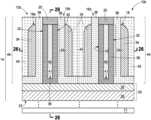
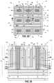
- FIG. 1is a diagrammatic cross-sectional view of a portion of a device comprising an array in accordance with an embodiment of the invention, and includes a portion taken through line 1 - 1 in FIGS. 2 and 7 .
- FIG. 2is an enlarged cross-sectional view taken through line 2 - 2 in FIGS. 1 and 3 - 6 .
- FIG. 3is a cross-sectional view including a portion taken through line 3 - 3 in FIGS. 2 and 7 .
- FIG. 4is a cross-sectional view including a portion taken through line 4 - 4 in FIGS. 2 and 7 .
- FIG. 5is a cross-sectional view including a portion taken through line 5 - 5 in FIGS. 2 and 7 .
- FIG. 6is a cross-sectional view including a portion taken through line 6 - 6 in FIGS. 2 and 7 .
- FIG. 7is a cross-sectional view taken through line 7 - 7 in FIGS. 1 and 2 .
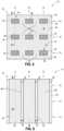
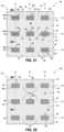
- FIG. 8is a diagrammatic hybrid schematic and cross-sectional view of a portion of a device comprising an array in accordance with an embodiment of the invention, and includes a portion taken through line 8 - 8 in FIGS. 9 and 14 .
- FIG. 9is an enlarged cross-sectional view taken through line 9 - 9 in FIGS. 8 and 10 - 12 .
- FIG. 10is a cross-sectional view including a portion taken through line 10 - 10 in FIGS. 9 , 13 , and 14 .
- FIG. 11is a cross-sectional view including a portion taken through line 11 - 11 in FIGS. 9 , 13 , and 14 .
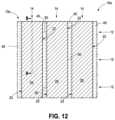
- FIG. 12is a cross-sectional view including a portion taken through line 12 - 12 in FIGS. 9 , 13 , and 14 .
- FIG. 13is a cross-sectional view taken through line 13 - 13 in FIG. 9 .
- FIG. 14is a cross-sectional view taken through line 14 - 14 in FIGS. 8 and 9 .
- FIG. 15is a diagrammatic cross-sectional view of a predecessor substrate to that shown by FIG. 8 , and includes a portion taken through line 15 - 15 in FIGS. 16 and 18 .
- FIG. 16is an enlarged cross-sectional view taken through line 16 - 16 in FIGS. 15 and 17 .
- FIG. 17is cross-sectional view including a portion taken through line 17 - 17 in FIGS. 16 and 18 .
- FIG. 18is a cross-sectional view taken through line 18 - 18 in FIG. 16 .
- FIG. 19is a view of the FIG. 15 substrate at a processing step subsequent to that shown by FIG. 15 , and includes a portion taken through line 19 - 19 in FIGS. 20 and 22 .
- FIG. 20is an enlarged cross-sectional view taken through line 20 - 20 in FIGS. 19 and 21 .
- FIG. 21is a cross-sectional view including a portion taken through line 21 - 21 in FIGS. 20 and 22 .
- FIG. 22is a cross-sectional view taken through line 22 - 22 in FIGS. 19 and 20 .
- FIG. 23is a view of the FIG. 20 substrate at a processing step subsequent to that shown by FIG. 20 .
- FIG. 24is cross-sectional view taken through line 24 - 24 in FIG. 23 .
- FIG. 25is cross-sectional view taken through line 25 - 25 in FIG. 23 .
- FIG. 26is a diagrammatic cross-sectional view of a portion of a device comprising an array in accordance with an embodiment of the invention, and includes a portion taken through line 26 - 26 in FIGS. 27 and 28 .
- FIG. 27is an enlarged cross-sectional view taken through line 27 - 27 in FIG. 26 .
- FIG. 28is a cross-sectional view taken through line 28 - 28 in FIGS. 26 and 27 .
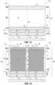
- FIG. 29is a diagrammatic cross-sectional view of a portion of a device comprising an array in accordance with an embodiment of the invention, and includes a portion taken through line 29 - 29 in FIG. 30 .
- FIG. 31is a cross-sectional view including a portion taken through line 31 - 31 in FIG. 30 .
- FIG. 32is a cross-sectional view including a portion taken through line 32 - 32 in FIG. 30 .
- Embodiments of the inventionencompass elevationally-extending transistors, devices comprising elevationally-extending transistors, and methods of forming a device comprising elevationally-extending transistors.
- a substrate fragment, construction, or device 10comprises a base substrate 11 that may include any one or more of conductive/conductor/conducting (i.e., electrically herein), semiconductive/semiconductor/semiconducting, or insulative/insulator/insulating (i.e., electrically herein) materials.
- Various materialshave been formed elevationally over base substrate 11 . Materials may be aside, elevationally inward, or elevationally outward of the FIGS. 1 - 7 —depicted materials.
- fabricated components of integrated circuitrymay be provided somewhere above, about, or within base substrate 11 .
- Control and/or other peripheral circuitry for operating components within an array of transistorsmay also be fabricated, and may or may not be wholly or partially within a transistor array or sub-array.
- multiple sub-arraysmay also be fabricated and operated independently, in tandem, or otherwise relative one another.
- a “sub-array”may also be considered as an array.
- Device 10comprises an array 13 comprising rows 12 and columns 14 of elevationally-extending transistors 16 . Portions of only nine transistors 16 are collectively visible in FIGS. 1 - 7 , with an array likely having thousands, hundreds of thousands, millions, etc. of transistors 16 .
- Example elevationally-extending transistors 16are shown as being arrayed in a 2D rectangular Bravais lattice, although any other existing or yet-do-be-developed arrangement may be used (e.g., a non-Bravais lattice or another 2D Bravais lattice such as oblique, centered rectangular, square, or hexagonal).
- An access line 18interconnects multiple elevationally-extending transistor 16 along individual rows 12 .
- Access lines 18may comprise any suitable conductive material (e.g., metal material and/or conductively-doped semiconductive material).
- conductive materiale.g., metal material and/or conductively-doped semiconductive material.
- Embodiments of the inventionencompass devices comprising an array, access lines, and elevationally-extending transistors, and as well elevationally-extending transistors independent of being fabricated relative to or within an array and independent of comprising an access line.
- Individual transistors 16comprises an upper source/drain region 20 , a lower source/drain region 22 , and a channel region 24 extending elevationally there-between.
- Upper source/drain region 20may be considered as comprising a top 59 .
- the source/drain regionsmay comprise any suitable conductive material (e.g., metal material and/or conductively-doped semiconductive material) and/or semiconductive material.
- lower source/drain region 22comprises a longitudinally elongated source line 23 extending along and interconnecting multiple elevationally-extending transistors 16 along individual columns 14 .
- Insulator material 45e.g., silicon dioxide and/or silicon nitride
- Example source/drain lines 23are shown as comprising an upper material 26 (e.g., elemental ruthenium) and a lower material 28 (e.g., conductively-doped silicon).
- Example channel regions 24individually comprise sides 30 , 31 , 32 , and 33 (i.e., in a straight-line vertical cross-section) with, for example, sides 30 , 32 comprising two opposing sides of channel region 24 and sides 31 , 33 comprising two opposing sides of channel region 24 .
- Channel region 24is shown as being rectangular in horizontal cross-section although other shapes may of course be used (e.g., any polygon, a structure have curved sides [e.g., a circle, ellipse, etc.], a combination of curved and straight sides, etc.).
- a transistor gate 34is over two opposing sides ( 30 , 32 and/or 31 , 33 ) of channel region 24 .
- transistor gate 34laterally surrounds channel region 24 and in one embodiment comprises a portion of an individual access line 18 .
- a gate insulator material 36e.g., silicon dioxide, silicon nitride, hafnium oxide, barium strontium titanate, other high-k dielectrics, etc. is over individual of the two opposing sides of channel region 24 laterally between channel region 24 and transistor gate 34 .
- the two opposing sides of channel region 24individually comprise an oxide semiconductor 38 (ideally amorphous).
- Example such materialsinclude ZnO x , InO x , In 2 O 3 , SnO 2 , TiO x , Zn x O y N z , Mg x Zn y O z , In x Zn y O z , In x Ga y Zn z O a , In x Ga y Si z O a , Zr x In y Zn z O a , Hf x In y Zn z O a , Sn x In y Zn z O a , Al x Sn y In z Zn a O d , Si x In y Zn z O a , Zn x Sn y O z , Al x Zn y Sn z O a , Ga x Zn y Sn z O a , and Z
- all sides 30 - 33 of channel region 24individually comprise an oxide semiconductor.
- the material designated with numeral 38may comprise, consist essentially of, or consist of an oxide semiconductor.
- suchmay comprise multiple different composition materials and/or regions, including for example different combinations of different composition oxide semiconductor materials (whether crystalline or amorphous) and/or combinations of oxide semiconductor materials with materials that are not oxide semiconductor materials.
- such other materialsmay not necessarily operably function as a channel of channel region 24 as long as channel region 24 overall is capable of functioning as a switchable channel determined by electric field applied thereto by gate 34 .
- an elevationally elongated void space 40is laterally between the two opposing sides of channel region 24 that comprises an oxide semiconductor.
- Void space 40may be considered as comprising a bottom 41 , and in one embodiment void space 40 is completely surrounded by oxide semiconductor of material 38 (i.e., in at least one straight-line horizontal cross-section; e.g., a horizontal cross-section shown by either of FIGS. 1 and 4 ).
- oxide semiconductor of material 38extends laterally across bottom 41 of void space 40 .
- oxide semiconductor of material 38is at least partially below gate 34 .
- oxide semiconductor of material 38is everywhere below gate 34 , and in one such embodiment is nowhere directly below gate 34 .
- void space 40is directly against oxide semiconductor of material 38 .
- the oxide semiconductorextends laterally across all of bottom 41 of void space 40 and longitudinally along all of bottom 41 of void space 40 .
- transistor 16is one transistor of an array 13 of a plurality of transistors 16 of like-construction relative one another.
- Intra-row-insulating material 42is longitudinally between immediately-intra-row-adjacent elevationally-extending transistor 16 .
- Inter-row-insulating material 44is laterally between immediately-adjacent rows 12 of elevationally-extending transistors 16 .
- Materials 42 and 44may be of the same or different composition(s) relative one another, with same composition being shown (e.g., each being a combination of insulator materials 45 and 36 ).
- Elevationally-extending transistors 16 and device 10may be manufactured using any suitable existing or yet-to-be-developed technique(s). Further, transistors 16 may be associated with or inherently comprise a data-storage device of existing or yet-to-be-developed circuitry, for example as part of memory circuitry. As examples, transistors 16 may individually comprise a reversibly programmable charge-storage region (not shown) between the gate insulator 36 and conductive gate 34 . Alternately or additionally, and by way of example only, gate insulator 36 may be ferroelectric. Further, and regardless, a capacitor (not shown) may be directly electrically coupled to source/drain region 20 , with an individual transistor and such capacitor forming a single memory cell. The capacitor insulator of the capacitor may be ferroelectric.
- Device 10 acomprises an array 13 a comprising rows 12 and columns 14 of elevationally-extending transistors 16 a .
- An access line 18 ainterconnects multiple elevationally-extending transistors 16 a along individual rows 12 .
- Transistors 16 aindividually comprise an upper source/drain region 20 , a lower source/drain region 22 , and a channel region 24 a extending elevationally there-between.
- Channel region 24 acomprises an oxide semiconductor 38 a .
- the example embodiments of FIGS. 8 - 14are shown as not comprising a void space 40 unlike that of the first-described embodiments, although alternately the embodiments of FIGS. 8 - 14 may have a void space 40 (not shown).
- a transistor gate 34 ais operatively laterally-proximate channel region 24 a (e.g., gate insulator 36 being between gate 34 a and channel 24 a ), and comprises a portion of an individual access line 18 a .
- transistor gate 34 ais over two opposing sides of channel region 24 a (e.g., only over two opposing sides 30 , 32 ).
- the transistor gatemay completely laterally surround (not shown) the channel region or may be over only one side (not shown) of channel region 24 a.
- intra-row-insulating material 42 a or inter-row-insulating material 44 amay comprise void space.
- the depicted laterally-spaced longitudinal portions of access lines 18 a in individual rows 12may be directly coupled with one another outside of array 13 , for example as shown by respective schematic interconnect lines 19 .
- immediately-intra-row-adjacent transistor 16 amay be considered as having a respective maximum intra-row-separation-distance 50 longitudinally between closest-operative-transistor material (e.g., any of materials 20 , 38 a , 22 , 26 , and/or 28 ).
- Such maximum distance 50may be the same for all row-adjacent transistors 16 a in a row 12 , or at least some such maximum separation distances may be different (not show).
- intra-row-insulating material 42 acomprises intra-row void space 46
- such intra-row void spaceindividually extends along at least 50%, and in one such embodiment along at least 75% (100% being shown), of the respective maximum intra-row-separation-distance 50 .
- An embodiment of the inventioncomprises a method of forming a device, for example, a device comprising array 13 a .
- An example such methodis described with reference to FIGS. 15 - 25 to result in an example finished construction of FIGS. 8 - 14 .
- Like numerals from the above-described embodimentshave been used for predecessor construction(s), regions, and like/predecessor materials thereof.
- Such a methodincludes forming an array comprising rows and columns of elevationally-extending transistors, and including an access line interconnecting multiple of the elevationally-extending transistors along individual of the rows. For example, and referring to FIGS.
- construction 10 ais initially formed to comprise oxide-semiconductor-channel-comprising material 38 a , gate insulator material 36 , access lines 18 a , lower source/drain lines 23 , and upper source/drain region material 20 running continuously in lines along individual rows 12 .
- intra-row void space 46is longitudinally between immediately-intra-row-adjacent elevationally-extending transistors 16 a .
- inter-row void space 48is laterally between immediately-adjacent rows 12 of elevationally-extending transistors 16 a.
- insulator material 45has been formed to bridge across (e.g., define) tops 55 of intra-row void space 46 and to bridge across (e.g., define) tops 57 of inter-row void space 48 , thereby leaving intra-row void space 46 and inter-row void space 48 there-below.
- insulator material 45may subsequently be elevationally-removed back at least to tops 59 of upper source/drain regions 20 , for example as shown in FIGS. 8 and 14 .
- the act of removingforms insulator material 45 and upper source/drain regions 20 to have respective elevationally-outermost surfaces that are planar and coplanar.
- a transistor gate 34is over two opposing sides (e.g., sides 30 , 32 and/or sides 31 , 33 ) of channel region 24 b .
- a gate insulator 36is over the individual two opposing sides of channel region 24 b laterally between channel region 24 b and transistor gate 34 .
- transistor gate 34comprises a portion of individual access lines 18 .
- An elevationally-elongated second material 60is aside channel-region-first material 38 .
- Second material 60has greater E g (E g being electronic band gap) than first material 38 .
- Second material 60may be an oxide semiconductor.
- example oxide semiconductorse.g., metal oxides
- Second material 60may comprise, consist essentially of, or consist of one or more metal oxides and/or one or more metal nitrides individually having greater E g than first material 38 .
- some of second material 60may comprise material having equal and/or lower E g than that of first material 38 as long as thickness of material 60 overall has Eg greater than that of first material 38 .
- the oxide semiconductor of first material 38 and second material 60are directly against one another. In one embodiment, the oxide semiconductor of first material 38 is directly against both of upper source/drain region 20 and lower source/drain region 22 . In one embodiment, second material 60 is directly against only one of the upper or lower source/drain regions, with such being shown in the example embodiment as being directly against only upper source/drain region 20 . In one embodiment, gate insulator 36 is ferroelectric and device 10 comprises memory. In one embodiment, E g of second material 60 is no more than 7 eV greater than the E g of first material 38 , and in one embodiment the E g of second material 60 is no more than 8.5 eV.
- any one or more of the elevationally-extending featuresis formed to be vertical or within 10° of vertical.
- the devices discussed abovemay be incorporated into electronic systems.
- Such electronic systemsmay be used in, for example, memory modules, device drivers, power modules, communication modems, processor modules, and application-specific modules, and may include multilayer, multichip modules.
- the electronic systemsmay be any of a broad range of systems, such as, for example, cameras, wireless devices, displays, chip sets, set top boxes, games, lighting, vehicles, clocks, televisions, cell phones, personal computers, automobiles, industrial control systems, aircraft, etc.
- “elevational”, “higher”, “upper”, “lower”, “top”, “atop”, “bottom”, “above”, “below”, “under”, “beneath”, “up”, and “down”are generally with reference to the vertical direction.
- “Horizontal”refers to a general direction (i.e., within 10 degrees) along a primary substrate surface and may be relative to which the substrate is processed during fabrication, and vertical is a direction generally orthogonal thereto.
- Reference to “exactly horizontal”is the direction along the primary substrate surface (i.e., no degrees there-from) and may be relative to which the substrate is processed during fabrication.
- “vertical” and “horizontal” as used hereinare generally perpendicular directions relative one another and independent of orientation of the substrate in three-dimensional space.
- “elevationally-extending” and “extending elevationally”refer to a direction that is angled away by at least 45° from exactly horizontal.
- “extend(ing) elevationally” and “elevationally-extending” with respect to a field effect transistorare with reference to orientation of the transistor's channel length along which current flows in operation between the source/drain regions.
- “extend(ing) elevationally” and “elevationally-extending”are with reference to orientation of the base length along which current flows in operation between the emitter and collector.
- any of the materials, regions, and structures described hereinmay be homogenous or non-homogenous, and regardless may be continuous or discontinuous over any material which such overlie. Further, unless otherwise stated, each material may be formed using any suitable or yet-to-be-developed technique, with atomic layer deposition, chemical vapor deposition, physical vapor deposition, epitaxial growth, diffusion doping, and ion implanting being examples.
- thicknessby itself (no preceding directional adjective) is defined as the mean straight-line distance through a given material or region perpendicularly from a closest surface of an immediately-adjacent material of different composition or of an immediately-adjacent region.
- various materials or regions described hereinmay be of substantially constant thickness or of variable thicknesses. If of variable thickness, thickness refers to average thickness unless otherwise indicated, and such material or region will have some minimum thickness and some maximum thickness due to the thickness being variable.
- different compositiononly requires those portions of two stated materials or regions that may be directly against one another to be chemically and/or physically different, for example if such materials or regions are not homogenous.
- “different composition”only requires that those portions of the two stated materials or regions that are closest to one another be chemically and/or physically different if such materials or regions are not homogenous.
- a material, region, or structureis “directly against” another when there is at least some physical touching contact of the stated materials, regions, or structures relative one another.
- “over”, “on”, “adjacent”, “along”, and “against” not preceded by “directly”encompass “directly against” as well as construction where intervening material(s), region(s), or structure(s) result(s) in no physical touching contact of the stated materials, regions, or structures relative one another.
- regions-materials-componentsare “electrically coupled” relative one another if in normal operation electric current is capable of continuously flowing from one to the other, and does so predominately by movement of subatomic positive and/or negative charges when such are sufficiently generated.
- Another electronic componentmay be between and electrically coupled to the regions-materials-components.
- regions-materials-componentsare referred to as being “directly electrically coupled”, no intervening electronic component (e.g., no diode, transistor, resistor, transducer, switch, fuse, etc.) is between the directly electrically coupled regions-materials-components.
- metal materialis any one or combination of an elemental metal, a mixture or an alloy of two or more elemental metals, and any conductive metal compound.
- rows and columnsare used synonymously with respect to any series of regions, components, and/or features independent of function.
- the rowsmay be straight and/or curved and/or parallel and/or not parallel relative one another, as may be the columns. Further, the rows and columns may intersect relative one another at 90° or at one or more other angles.
- a devicecomprises an array comprising rows and columns of elevationally-extending transistors.
- An access lineinterconnects multiple of the elevationally-extending transistors along individual of the rows.
- the transistorsindividually comprise an upper source/drain region, a lower source/drain region, and a channel region extending elevationally there-between.
- the channel regioncomprises an oxide semiconductor.
- a transistor gateis operatively laterally-proximate the channel region and comprises a portion of an individual of the access lines.
- Intra-row-insulating materialis longitudinally between immediately-intra-row-adjacent of the elevationally-extending transistors.
- Inter-row-insulating materialis laterally between immediately-adjacent of the rows of the elevationally-extending transistors. At least one of the intra-row-insulating material and the inter-row-insulating material comprises void space.
- an elevationally-extending transistorcomprises an upper source/drain region, a lower source/drain region, and a channel region extending elevationally there-between.
- a transistor gateis over two opposing sides of the channel region.
- a gate insulatoris over individual of the two opposing sides of the channel region laterally between the channel region and the transistor gate.
- the two opposing sides of the channel regionindividually comprise an oxide semiconductor.
- An elevationally-elongated void spaceis laterally between the two opposing sides of the channel region. The oxide semiconductor extending laterally across a bottom of the void space.
- a devicecomprises an array comprising rows and columns of elevationally-extending transistors.
- An access lineinterconnects multiple of the elevationally-extending transistors along individual of the rows.
- the transistorsindividually comprise an upper source/drain region, a lower source/drain region, and a channel region extending elevationally there-between.
- a transistor gateis over two opposing sides of the channel region.
- a gate insulatoris over individual of the two opposing sides of the channel region laterally between the channel region and the transistor gate.
- the transistor gatecomprises a portion of an individual of the access lines.
- the two opposing sides of the channel regionindividually comprise an oxide semiconductor.
- An elevationally-elongated void spaceis laterally between the two opposing sides of the channel region.
- an elevationally-extending transistorcomprises an upper source/drain region, a lower source/drain region, and a channel region extending elevationally there-between.
- the channel regioncomprises an elevationally-elongated first material comprising an oxide semiconductor.
- a transistor gateis over two opposing sides of the channel region.
- a gate insulatoris over individual of the two opposing sides of the channel region laterally between the channel region and the transistor gate.
- An elevationally-elongated second materialis aside the channel-region-first material. The second material has greater E g than the first material.
- a devicecomprises an array comprising rows and columns of elevationally-extending transistors.
- An access lineinterconnects multiple of the elevationally-extending transistors along individual of the rows.
- the transistorsindividually comprise an upper source/drain region, a lower source/drain region, and a channel region extending elevationally there-between.
- the channel regioncomprises an elevationally-elongated first material comprising an oxide semiconductor.
- a transistor gateis over two opposing sides of the channel region.
- a gate insulatoris over individual of the two opposing sides of the channel region laterally between the channel region and the transistor gate.
- the transistor gatecomprises a portion of an individual of the access lines.
- An elevationally-elongated second materialis aside the channel-region-first material. The second material has greater E g than the first material.
- a method of forming a devicecomprises forming an array comprising rows and columns of elevationally-extending transistors, with an access line interconnecting multiple of the elevationally-extending transistors along individual of the rows.
- the transistorsindividually comprise an upper source/drain region, a lower source/drain region, and a channel region extending elevationally there-between.
- the channel regioncomprises an oxide semiconductor.
- a transistor gateis operatively laterally proximate the channel region and comprises a portion of an individual of the access lines.
- Intra-row void spaceis longitudinally between immediately-intra-row-adjacent of the elevationally-extending transistors.
- Inter-row void spaceis laterally between immediately-adjacent of the rows of the elevationally-extending transistors. Insulator material is formed to bridge across tops of the intra-row void space and to bridge across tops of the inter-row void space and leave the intra-row void space and the inter-row void space there-below.
Landscapes
- Engineering & Computer Science (AREA)
- Physics & Mathematics (AREA)
- Condensed Matter Physics & Semiconductors (AREA)
- General Physics & Mathematics (AREA)
- Manufacturing & Machinery (AREA)
- Computer Hardware Design (AREA)
- Microelectronics & Electronic Packaging (AREA)
- Power Engineering (AREA)
- Thin Film Transistor (AREA)
- Bipolar Transistors (AREA)
Abstract
Description
Claims (4)
Priority Applications (2)
| Application Number | Priority Date | Filing Date | Title |
|---|---|---|---|
| US17/472,895US12199182B2 (en) | 2018-10-09 | 2021-09-13 | Elevationally-extending transistors, devices comprising elevationally-extending transistors, and methods of forming a device comprising elevationally-extending transistors |
| US18/966,496US20250098228A1 (en) | 2018-10-09 | 2024-12-03 | Elevationally-Extending Transistors, Devices Comprising Elevationally-Extending Transistors, and Methods of Forming a Device Comprising Elevationally-Extending Transistors |
Applications Claiming Priority (3)
| Application Number | Priority Date | Filing Date | Title |
|---|---|---|---|
| US16/154,924US10629732B1 (en) | 2018-10-09 | 2018-10-09 | Elevationally-extending transistors, devices comprising elevationally-extending transistors, and methods of forming a device comprising elevationally-extending transistors |
| US16/826,011US11152509B2 (en) | 2018-10-09 | 2020-03-20 | Elevationally-extending transistors, devices comprising elevationally-extending transistors, and methods of forming a device comprising elevationally-extending transistors |
| US17/472,895US12199182B2 (en) | 2018-10-09 | 2021-09-13 | Elevationally-extending transistors, devices comprising elevationally-extending transistors, and methods of forming a device comprising elevationally-extending transistors |
Related Parent Applications (1)
| Application Number | Title | Priority Date | Filing Date |
|---|---|---|---|
| US16/826,011DivisionUS11152509B2 (en) | 2018-10-09 | 2020-03-20 | Elevationally-extending transistors, devices comprising elevationally-extending transistors, and methods of forming a device comprising elevationally-extending transistors |
Related Child Applications (1)
| Application Number | Title | Priority Date | Filing Date |
|---|---|---|---|
| US18/966,496ContinuationUS20250098228A1 (en) | 2018-10-09 | 2024-12-03 | Elevationally-Extending Transistors, Devices Comprising Elevationally-Extending Transistors, and Methods of Forming a Device Comprising Elevationally-Extending Transistors |
Publications (2)
| Publication Number | Publication Date |
|---|---|
| US20210408294A1 US20210408294A1 (en) | 2021-12-30 |
| US12199182B2true US12199182B2 (en) | 2025-01-14 |
Family
ID=70051841
Family Applications (4)
| Application Number | Title | Priority Date | Filing Date |
|---|---|---|---|
| US16/154,924ActiveUS10629732B1 (en) | 2018-10-09 | 2018-10-09 | Elevationally-extending transistors, devices comprising elevationally-extending transistors, and methods of forming a device comprising elevationally-extending transistors |
| US16/826,011Active2038-10-14US11152509B2 (en) | 2018-10-09 | 2020-03-20 | Elevationally-extending transistors, devices comprising elevationally-extending transistors, and methods of forming a device comprising elevationally-extending transistors |
| US17/472,895Active2039-02-28US12199182B2 (en) | 2018-10-09 | 2021-09-13 | Elevationally-extending transistors, devices comprising elevationally-extending transistors, and methods of forming a device comprising elevationally-extending transistors |
| US18/966,496PendingUS20250098228A1 (en) | 2018-10-09 | 2024-12-03 | Elevationally-Extending Transistors, Devices Comprising Elevationally-Extending Transistors, and Methods of Forming a Device Comprising Elevationally-Extending Transistors |
Family Applications Before (2)
| Application Number | Title | Priority Date | Filing Date |
|---|---|---|---|
| US16/154,924ActiveUS10629732B1 (en) | 2018-10-09 | 2018-10-09 | Elevationally-extending transistors, devices comprising elevationally-extending transistors, and methods of forming a device comprising elevationally-extending transistors |
| US16/826,011Active2038-10-14US11152509B2 (en) | 2018-10-09 | 2020-03-20 | Elevationally-extending transistors, devices comprising elevationally-extending transistors, and methods of forming a device comprising elevationally-extending transistors |
Family Applications After (1)
| Application Number | Title | Priority Date | Filing Date |
|---|---|---|---|
| US18/966,496PendingUS20250098228A1 (en) | 2018-10-09 | 2024-12-03 | Elevationally-Extending Transistors, Devices Comprising Elevationally-Extending Transistors, and Methods of Forming a Device Comprising Elevationally-Extending Transistors |
Country Status (6)
| Country | Link |
|---|---|
| US (4) | US10629732B1 (en) |
| EP (1) | EP3864701A4 (en) |
| KR (1) | KR20210057827A (en) |
| CN (1) | CN112913027B (en) |
| TW (1) | TWI768250B (en) |
| WO (1) | WO2020076615A1 (en) |
Families Citing this family (11)
| Publication number | Priority date | Publication date | Assignee | Title |
|---|---|---|---|---|
| US11488981B2 (en)* | 2020-07-21 | 2022-11-01 | Micron Technology, Inc. | Array of vertical transistors and method used in forming an array of vertical transistors |
| KR20220169503A (en)* | 2021-06-18 | 2022-12-28 | 삼성전자주식회사 | Semiconductor devices |
| US12015081B2 (en)* | 2021-07-15 | 2024-06-18 | Taiwan Semiconductor Manufacturing Company, Ltd. | Semiconductor device and manufacturing method thereof |
| US11839071B2 (en)* | 2021-07-22 | 2023-12-05 | Taiwan Semiconductor Manufacturing Company Limited | Vertical access transistors and methods for forming the same |
| CN116960052A (en)* | 2022-04-12 | 2023-10-27 | 北京超弦存储器研究院 | Semiconductor structure manufacturing method and semiconductor structure |
| CN114927477A (en) | 2022-05-06 | 2022-08-19 | 长鑫存储技术有限公司 | Preparation method of semiconductor device, semiconductor device and stacked device |
| EP4461105A4 (en)* | 2022-05-19 | 2025-06-18 | Yangtze Memory Technologies Co., Ltd. | MEMORY DEVICES COMPRISING VERTICAL TRANSISTORS AND METHODS OF FORMING THE SAME |
| WO2023221925A1 (en)* | 2022-05-19 | 2023-11-23 | Yangtze Memory Technologies Co., Ltd. | Memory devices having vertical transistors and methods for forming the same |
| CN115224110A (en)* | 2022-07-19 | 2022-10-21 | 长江存储科技有限责任公司 | Semiconductor structure and manufacturing method, memory and manufacturing method, and memory system |
| KR20240073322A (en)* | 2022-11-18 | 2024-05-27 | 삼성전자주식회사 | Semiconductor memory device |
| CN115939174B (en)* | 2022-12-20 | 2025-09-16 | 福建省晋华集成电路有限公司 | Semiconductor device and method for manufacturing the same |
Citations (25)
| Publication number | Priority date | Publication date | Assignee | Title |
|---|---|---|---|---|
| US20090097309A1 (en)* | 2007-10-03 | 2009-04-16 | Kabushiki Kaisha Toshiba | Nonvolatile semiconductor storage device, and method for controlling nonvolatile semiconductor storage device |
| US20120205713A1 (en) | 2011-02-11 | 2012-08-16 | Micron Technology, Inc. | Memory Cells, Memory Arrays, Methods Of Forming Memory Cells, And Methods Of Forming A Shared Doped Semiconductor Region Of A Vertically Oriented Thyristor And A Vertically Oriented Access Transistor |
| WO2013188654A1 (en) | 2012-06-15 | 2013-12-19 | Sandisk 3D Llc | 3d memory having vertical switches with surround gates and method thereof |
| KR20140036320A (en) | 2011-08-23 | 2014-03-25 | 마이크론 테크놀로지, 인크. | Semiconductor device structures including vertical transistor devices, arrays of vertical transistor devices, and methods of fabrication |
| US20140106554A1 (en) | 2012-10-15 | 2014-04-17 | Micron Technology, Inc. | Methods of Forming Gated Devices |
| US20150200308A1 (en)* | 2014-01-10 | 2015-07-16 | Micron Technology, Inc. | Field Effect Transistor Constructions And Memory Arrays |
| US20150243748A1 (en) | 2014-02-26 | 2015-08-27 | Micron Technology, Inc. | Vertical access devices, semiconductor device structures, and related methods |
| US20150311349A1 (en) | 2014-04-24 | 2015-10-29 | Micron Technology, Inc. | Ferroelectric Field Effect Transistors, Pluralities Of Ferroelectric Field Effect Transistors Arrayed In Row Lines And Column Lines, And Methods Of Forming A Plurality Of Ferroelectric Field Effect Transistors |
| US20150311316A1 (en) | 2013-08-19 | 2015-10-29 | SK Hynix Inc. | Variable resistive memory device including vertical channel pmos transistor and method of manufacturing the same |
| US9177872B2 (en) | 2011-09-16 | 2015-11-03 | Micron Technology, Inc. | Memory cells, semiconductor devices, systems including such cells, and methods of fabrication |
| US9276092B1 (en) | 2014-10-16 | 2016-03-01 | Micron Technology, Inc. | Transistors and methods of forming transistors |
| US20160064406A1 (en) | 2014-09-02 | 2016-03-03 | Kabushiki Kaisha Toshiba | Semiconductor memory device and method for manufacturing the same |
| US20160268500A1 (en) | 2015-03-09 | 2016-09-15 | Kabushiki Kaisha Toshiba | Resistance change memory |
| US20160372519A1 (en) | 2015-04-10 | 2016-12-22 | SK Hynix Inc. | Method of manufacturing a semiconductor integrated circuit device including a transistor with a vertical channel |
| US20170040416A1 (en)* | 2015-08-04 | 2017-02-09 | Kabushiki Kaisha Toshiba | Semiconductor memory device |
| US20170062459A1 (en) | 2015-08-26 | 2017-03-02 | Kabushiki Kaisha Toshiba | Semiconductor device and method for manufacturing same |
| US20170148517A1 (en) | 2015-11-25 | 2017-05-25 | Eli Harari | Three-dimensional vertical nor flash thin film transistor strings |
| US9673054B2 (en) | 2014-08-18 | 2017-06-06 | Micron Technology, Inc. | Array of gated devices and methods of forming an array of gated devices |
| US9837422B2 (en) | 2011-12-09 | 2017-12-05 | SK Hynix Inc. | Method for forming buried bit line, semiconductor device having the same, and fabricating method thereof |
| WO2018118097A1 (en) | 2016-12-24 | 2018-06-28 | Intel Corporation | Vertical transistor devices and techniques |
| US20190067303A1 (en) | 2017-08-29 | 2019-02-28 | Micron Technology, Inc. | Methods Used In Forming An Array Of Memory Cells |
| US20190067437A1 (en)* | 2017-08-31 | 2019-02-28 | Micron Technology, Inc. | Semiconductor devices, transistors, and related methods for contacting metal oxide semiconductor devices |
| US20200258980A1 (en) | 2017-08-11 | 2020-08-13 | Micron Technology, Inc. | Memory device including voids between control gates |
| US20200312876A1 (en) | 2018-02-02 | 2020-10-01 | Sunrise Memory Corporation | Three-dimensional vertical NOR Flash Thin-Film Transistor Strings |
| US20210104608A1 (en)* | 2017-06-05 | 2021-04-08 | Semiconductor Energy Laboratory Co., Ltd. | Semiconductor device, and method of manufacturing the semiconductor device |
- 2018
- 2018-10-09USUS16/154,924patent/US10629732B1/enactiveActive
- 2019
- 2019-10-03EPEP19871317.4Apatent/EP3864701A4/ennot_activeWithdrawn
- 2019-10-03WOPCT/US2019/054557patent/WO2020076615A1/ennot_activeCeased
- 2019-10-03CNCN201980070109.3Apatent/CN112913027B/enactiveActive
- 2019-10-03KRKR1020217013854Apatent/KR20210057827A/ennot_activeCeased
- 2019-10-08TWTW108136370Apatent/TWI768250B/enactive
- 2020
- 2020-03-20USUS16/826,011patent/US11152509B2/enactiveActive
- 2021
- 2021-09-13USUS17/472,895patent/US12199182B2/enactiveActive
- 2024
- 2024-12-03USUS18/966,496patent/US20250098228A1/enactivePending
Patent Citations (33)
| Publication number | Priority date | Publication date | Assignee | Title |
|---|---|---|---|---|
| US20090097309A1 (en)* | 2007-10-03 | 2009-04-16 | Kabushiki Kaisha Toshiba | Nonvolatile semiconductor storage device, and method for controlling nonvolatile semiconductor storage device |
| US20120205713A1 (en) | 2011-02-11 | 2012-08-16 | Micron Technology, Inc. | Memory Cells, Memory Arrays, Methods Of Forming Memory Cells, And Methods Of Forming A Shared Doped Semiconductor Region Of A Vertically Oriented Thyristor And A Vertically Oriented Access Transistor |
| KR20140036320A (en) | 2011-08-23 | 2014-03-25 | 마이크론 테크놀로지, 인크. | Semiconductor device structures including vertical transistor devices, arrays of vertical transistor devices, and methods of fabrication |
| US20160276454A1 (en) | 2011-08-23 | 2016-09-22 | Micron Technology, Inc. | Semiconductor devices and structures and methods of formation |
| US20210273111A1 (en) | 2011-08-23 | 2021-09-02 | Micron Technology, Inc. | Methods of forming a semiconductor device comprising a channel material |
| US9177872B2 (en) | 2011-09-16 | 2015-11-03 | Micron Technology, Inc. | Memory cells, semiconductor devices, systems including such cells, and methods of fabrication |
| US9837422B2 (en) | 2011-12-09 | 2017-12-05 | SK Hynix Inc. | Method for forming buried bit line, semiconductor device having the same, and fabricating method thereof |
| US20180053770A1 (en) | 2011-12-09 | 2018-02-22 | SK Hynix Inc. | Method for forming buried bit line, semiconductor device having the same, and fabricating method thereof |
| WO2013188654A1 (en) | 2012-06-15 | 2013-12-19 | Sandisk 3D Llc | 3d memory having vertical switches with surround gates and method thereof |
| US20140106554A1 (en) | 2012-10-15 | 2014-04-17 | Micron Technology, Inc. | Methods of Forming Gated Devices |
| US20150311316A1 (en) | 2013-08-19 | 2015-10-29 | SK Hynix Inc. | Variable resistive memory device including vertical channel pmos transistor and method of manufacturing the same |
| TW201535679A (en) | 2014-01-10 | 2015-09-16 | Micron Technology Inc | Field effect transistor structure and memory array |
| US20150200308A1 (en)* | 2014-01-10 | 2015-07-16 | Micron Technology, Inc. | Field Effect Transistor Constructions And Memory Arrays |
| US9773888B2 (en) | 2014-02-26 | 2017-09-26 | Micron Technology, Inc. | Vertical access devices, semiconductor device structures, and related methods |
| US20150243748A1 (en) | 2014-02-26 | 2015-08-27 | Micron Technology, Inc. | Vertical access devices, semiconductor device structures, and related methods |
| US20150311349A1 (en) | 2014-04-24 | 2015-10-29 | Micron Technology, Inc. | Ferroelectric Field Effect Transistors, Pluralities Of Ferroelectric Field Effect Transistors Arrayed In Row Lines And Column Lines, And Methods Of Forming A Plurality Of Ferroelectric Field Effect Transistors |
| CN106463510A (en) | 2014-04-24 | 2017-02-22 | 美光科技公司 | Ferroelectric field effect transistor, a plurality of ferroelectric field effect transistors in an array in row and column lines, and a method of forming a plurality of ferroelectric field effect transistors |
| US9673054B2 (en) | 2014-08-18 | 2017-06-06 | Micron Technology, Inc. | Array of gated devices and methods of forming an array of gated devices |
| US20160064406A1 (en) | 2014-09-02 | 2016-03-03 | Kabushiki Kaisha Toshiba | Semiconductor memory device and method for manufacturing the same |
| CN106796957A (en) | 2014-10-16 | 2017-05-31 | 美光科技公司 | Transistor and method of forming transistor |
| US9276092B1 (en) | 2014-10-16 | 2016-03-01 | Micron Technology, Inc. | Transistors and methods of forming transistors |
| US20160268500A1 (en) | 2015-03-09 | 2016-09-15 | Kabushiki Kaisha Toshiba | Resistance change memory |
| US20160372519A1 (en) | 2015-04-10 | 2016-12-22 | SK Hynix Inc. | Method of manufacturing a semiconductor integrated circuit device including a transistor with a vertical channel |
| US20170040416A1 (en)* | 2015-08-04 | 2017-02-09 | Kabushiki Kaisha Toshiba | Semiconductor memory device |
| US20170062459A1 (en) | 2015-08-26 | 2017-03-02 | Kabushiki Kaisha Toshiba | Semiconductor device and method for manufacturing same |
| US20170148517A1 (en) | 2015-11-25 | 2017-05-25 | Eli Harari | Three-dimensional vertical nor flash thin film transistor strings |
| WO2018118097A1 (en) | 2016-12-24 | 2018-06-28 | Intel Corporation | Vertical transistor devices and techniques |
| US20200058798A1 (en) | 2016-12-24 | 2020-02-20 | Intel Corporation | Vertical transistor devices and techniques |
| US20210104608A1 (en)* | 2017-06-05 | 2021-04-08 | Semiconductor Energy Laboratory Co., Ltd. | Semiconductor device, and method of manufacturing the semiconductor device |
| US20200258980A1 (en) | 2017-08-11 | 2020-08-13 | Micron Technology, Inc. | Memory device including voids between control gates |
| US20190067303A1 (en) | 2017-08-29 | 2019-02-28 | Micron Technology, Inc. | Methods Used In Forming An Array Of Memory Cells |
| US20190067437A1 (en)* | 2017-08-31 | 2019-02-28 | Micron Technology, Inc. | Semiconductor devices, transistors, and related methods for contacting metal oxide semiconductor devices |
| US20200312876A1 (en) | 2018-02-02 | 2020-10-01 | Sunrise Memory Corporation | Three-dimensional vertical NOR Flash Thin-Film Transistor Strings |
Non-Patent Citations (5)
| Title |
|---|
| Park et al., "Overview of electroceramic materials for oxide semiconductor thin film transistors", Journal of Electroceramics, Sep. 24, 2013, Netherlands, pp. 117-140. |
| TW 108136370 Search Report, Sep. 21, 2020, Micron Technology, Inc. |
| WO PCT/US2019/054557 IPRP, Apr. 8, 2021, Micron Technology, Inc. |
| WO PCT/US2019/054557 SR, Jan. 23, 2020, Micron Technology, Inc. |
| WO PCT/US2019/054557 WO, Jan. 23, 2020, Micron Technology, Inc. |
Also Published As
| Publication number | Publication date |
|---|---|
| KR20210057827A (en) | 2021-05-21 |
| US10629732B1 (en) | 2020-04-21 |
| WO2020076615A8 (en) | 2021-04-22 |
| TWI768250B (en) | 2022-06-21 |
| US20200220022A1 (en) | 2020-07-09 |
| TW202038436A (en) | 2020-10-16 |
| US20210408294A1 (en) | 2021-12-30 |
| EP3864701A4 (en) | 2022-11-02 |
| US11152509B2 (en) | 2021-10-19 |
| WO2020076615A1 (en) | 2020-04-16 |
| EP3864701A1 (en) | 2021-08-18 |
| US20200111915A1 (en) | 2020-04-09 |
| CN112913027A (en) | 2021-06-04 |
| CN112913027B (en) | 2024-01-26 |
| US20250098228A1 (en) | 2025-03-20 |
Similar Documents
| Publication | Publication Date | Title |
|---|---|---|
| US12199182B2 (en) | Elevationally-extending transistors, devices comprising elevationally-extending transistors, and methods of forming a device comprising elevationally-extending transistors | |
| US11864386B2 (en) | Memory arrays | |
| US20220130845A1 (en) | Array Of Capacitors, Array Of Memory Cells, Methods Of Forming An Array Of Capacitors, And Methods Of Forming An Array Of Memory Cells | |
| KR20190034706A (en) | Recessed transistors containing ferroelectric material | |
| CN111048522A (en) | A plurality of ferroelectric field effect transistors forming an array and a method of forming the same | |
| US20220278001A1 (en) | Array Of Vertical Transistors, An Array Of Memory Cells Comprising An Array Of Vertical Transistors, And A Method Used In Forming An Array Of Vertical Transistors | |
| US20250275249A1 (en) | Array Of Vertical Transistors And Method Used In Forming An Array Of Vertical Transistors | |
| CN112447716A (en) | Vertical transistor array and method of forming a vertical transistor array | |
| US20240164114A1 (en) | Vertical Transistor, Integrated Circuitry, Method Of Forming A Vertical Transistor, And Method Of Forming Integrated Circuitry | |
| US10777562B1 (en) | Integrated circuity, DRAM circuitry, methods used in forming integrated circuitry, and methods used in forming DRAM circuitry | |
| US20240276714A1 (en) | DRAM Circuitry And Method Of Forming DRAM Circuitry | |
| US20220102348A1 (en) | Integrated Circuitry, Memory Circuitry, Method Used In Forming Integrated Circuitry, And Method Used In Forming Memory Circuitry | |
| US20250261410A1 (en) | Ferroelectric Transistor, Memory Circuitry Comprising Ferroelectric Transistors, And Method Used In Forming Memory Circuitry Comprising Memory Cells That Individually Comprise A Horizontal Ferroelectric Transistor | |
| US20250324607A1 (en) | Ferroelectric Memory Circuitry And Method Used In Forming Ferroelectric Memory Circuitry | |
| US20230422483A1 (en) | Memory Circuitry And Method Used In Forming Memory Circuitry | |
| US20230207699A1 (en) | Transistors, Array Of Transistors, And Array Of Memory Cells Individually Comprising A Transistor |
Legal Events
| Date | Code | Title | Description |
|---|---|---|---|
| FEPP | Fee payment procedure | Free format text:ENTITY STATUS SET TO UNDISCOUNTED (ORIGINAL EVENT CODE: BIG.); ENTITY STATUS OF PATENT OWNER: LARGE ENTITY | |
| STPP | Information on status: patent application and granting procedure in general | Free format text:DOCKETED NEW CASE - READY FOR EXAMINATION | |
| STPP | Information on status: patent application and granting procedure in general | Free format text:RESPONSE TO NON-FINAL OFFICE ACTION ENTERED AND FORWARDED TO EXAMINER | |
| STPP | Information on status: patent application and granting procedure in general | Free format text:NON FINAL ACTION MAILED | |
| STPP | Information on status: patent application and granting procedure in general | Free format text:RESPONSE TO NON-FINAL OFFICE ACTION ENTERED AND FORWARDED TO EXAMINER | |
| STPP | Information on status: patent application and granting procedure in general | Free format text:FINAL REJECTION MAILED | |
| STPP | Information on status: patent application and granting procedure in general | Free format text:ADVISORY ACTION MAILED | |
| STPP | Information on status: patent application and granting procedure in general | Free format text:NON FINAL ACTION MAILED | |
| STPP | Information on status: patent application and granting procedure in general | Free format text:RESPONSE TO NON-FINAL OFFICE ACTION ENTERED AND FORWARDED TO EXAMINER | |
| STPP | Information on status: patent application and granting procedure in general | Free format text:FINAL REJECTION MAILED | |
| STPP | Information on status: patent application and granting procedure in general | Free format text:RESPONSE AFTER FINAL ACTION FORWARDED TO EXAMINER | |
| STPP | Information on status: patent application and granting procedure in general | Free format text:RESPONSE AFTER FINAL ACTION FORWARDED TO EXAMINER | |
| STPP | Information on status: patent application and granting procedure in general | Free format text:NOTICE OF ALLOWANCE MAILED -- APPLICATION RECEIVED IN OFFICE OF PUBLICATIONS | |
| ZAAB | Notice of allowance mailed | Free format text:ORIGINAL CODE: MN/=. | |
| STPP | Information on status: patent application and granting procedure in general | Free format text:PUBLICATIONS -- ISSUE FEE PAYMENT RECEIVED | |
| STPP | Information on status: patent application and granting procedure in general | Free format text:PUBLICATIONS -- ISSUE FEE PAYMENT VERIFIED | |
| STCF | Information on status: patent grant | Free format text:PATENTED CASE |