US12197681B2 - Anchor configurations for an array of ultrasonic transducers - Google Patents
Anchor configurations for an array of ultrasonic transducersDownload PDFInfo
- Publication number
- US12197681B2 US12197681B2US17/822,127US202217822127AUS12197681B2US 12197681 B2US12197681 B2US 12197681B2US 202217822127 AUS202217822127 AUS 202217822127AUS 12197681 B2US12197681 B2US 12197681B2
- Authority
- US
- United States
- Prior art keywords
- ultrasonic transducer
- anchor
- anchors
- ultrasonic
- electrode
- Prior art date
- Legal status (The legal status is an assumption and is not a legal conclusion. Google has not performed a legal analysis and makes no representation as to the accuracy of the status listed.)
- Active, expires
Links
Images


Classifications
- G—PHYSICS
- G01—MEASURING; TESTING
- G01H—MEASUREMENT OF MECHANICAL VIBRATIONS OR ULTRASONIC, SONIC OR INFRASONIC WAVES
- G01H11/00—Measuring mechanical vibrations or ultrasonic, sonic or infrasonic waves by detecting changes in electric or magnetic properties
- G01H11/06—Measuring mechanical vibrations or ultrasonic, sonic or infrasonic waves by detecting changes in electric or magnetic properties by electric means
- G01H11/08—Measuring mechanical vibrations or ultrasonic, sonic or infrasonic waves by detecting changes in electric or magnetic properties by electric means using piezoelectric devices
- G—PHYSICS
- G06—COMPUTING OR CALCULATING; COUNTING
- G06F—ELECTRIC DIGITAL DATA PROCESSING
- G06F3/00—Input arrangements for transferring data to be processed into a form capable of being handled by the computer; Output arrangements for transferring data from processing unit to output unit, e.g. interface arrangements
- G06F3/01—Input arrangements or combined input and output arrangements for interaction between user and computer
- G06F3/03—Arrangements for converting the position or the displacement of a member into a coded form
- G06F3/041—Digitisers, e.g. for touch screens or touch pads, characterised by the transducing means
- G06F3/043—Digitisers, e.g. for touch screens or touch pads, characterised by the transducing means using propagating acoustic waves
- G06F3/0436—Digitisers, e.g. for touch screens or touch pads, characterised by the transducing means using propagating acoustic waves in which generating transducers and detecting transducers are attached to a single acoustic waves transmission substrate
- A—HUMAN NECESSITIES
- A61—MEDICAL OR VETERINARY SCIENCE; HYGIENE
- A61B—DIAGNOSIS; SURGERY; IDENTIFICATION
- A61B8/00—Diagnosis using ultrasonic, sonic or infrasonic waves
- A61B8/44—Constructional features of the ultrasonic, sonic or infrasonic diagnostic device
- A61B8/4483—Constructional features of the ultrasonic, sonic or infrasonic diagnostic device characterised by features of the ultrasound transducer
- B—PERFORMING OPERATIONS; TRANSPORTING
- B06—GENERATING OR TRANSMITTING MECHANICAL VIBRATIONS IN GENERAL
- B06B—METHODS OR APPARATUS FOR GENERATING OR TRANSMITTING MECHANICAL VIBRATIONS OF INFRASONIC, SONIC, OR ULTRASONIC FREQUENCY, e.g. FOR PERFORMING MECHANICAL WORK IN GENERAL
- B06B1/00—Methods or apparatus for generating mechanical vibrations of infrasonic, sonic, or ultrasonic frequency
- B06B1/02—Methods or apparatus for generating mechanical vibrations of infrasonic, sonic, or ultrasonic frequency making use of electrical energy
- B06B1/0207—Driving circuits
- B—PERFORMING OPERATIONS; TRANSPORTING
- B06—GENERATING OR TRANSMITTING MECHANICAL VIBRATIONS IN GENERAL
- B06B—METHODS OR APPARATUS FOR GENERATING OR TRANSMITTING MECHANICAL VIBRATIONS OF INFRASONIC, SONIC, OR ULTRASONIC FREQUENCY, e.g. FOR PERFORMING MECHANICAL WORK IN GENERAL
- B06B1/00—Methods or apparatus for generating mechanical vibrations of infrasonic, sonic, or ultrasonic frequency
- B06B1/02—Methods or apparatus for generating mechanical vibrations of infrasonic, sonic, or ultrasonic frequency making use of electrical energy
- B06B1/06—Methods or apparatus for generating mechanical vibrations of infrasonic, sonic, or ultrasonic frequency making use of electrical energy operating with piezoelectric effect or with electrostriction
- B06B1/0607—Methods or apparatus for generating mechanical vibrations of infrasonic, sonic, or ultrasonic frequency making use of electrical energy operating with piezoelectric effect or with electrostriction using multiple elements
- B06B1/0611—Methods or apparatus for generating mechanical vibrations of infrasonic, sonic, or ultrasonic frequency making use of electrical energy operating with piezoelectric effect or with electrostriction using multiple elements in a pile
- B—PERFORMING OPERATIONS; TRANSPORTING
- B06—GENERATING OR TRANSMITTING MECHANICAL VIBRATIONS IN GENERAL
- B06B—METHODS OR APPARATUS FOR GENERATING OR TRANSMITTING MECHANICAL VIBRATIONS OF INFRASONIC, SONIC, OR ULTRASONIC FREQUENCY, e.g. FOR PERFORMING MECHANICAL WORK IN GENERAL
- B06B1/00—Methods or apparatus for generating mechanical vibrations of infrasonic, sonic, or ultrasonic frequency
- B06B1/02—Methods or apparatus for generating mechanical vibrations of infrasonic, sonic, or ultrasonic frequency making use of electrical energy
- B06B1/06—Methods or apparatus for generating mechanical vibrations of infrasonic, sonic, or ultrasonic frequency making use of electrical energy operating with piezoelectric effect or with electrostriction
- B06B1/0644—Methods or apparatus for generating mechanical vibrations of infrasonic, sonic, or ultrasonic frequency making use of electrical energy operating with piezoelectric effect or with electrostriction using a single piezoelectric element
- B06B1/0662—Methods or apparatus for generating mechanical vibrations of infrasonic, sonic, or ultrasonic frequency making use of electrical energy operating with piezoelectric effect or with electrostriction using a single piezoelectric element with an electrode on the sensitive surface
- B06B1/0674—Methods or apparatus for generating mechanical vibrations of infrasonic, sonic, or ultrasonic frequency making use of electrical energy operating with piezoelectric effect or with electrostriction using a single piezoelectric element with an electrode on the sensitive surface and a low impedance backing, e.g. air
- B—PERFORMING OPERATIONS; TRANSPORTING
- B06—GENERATING OR TRANSMITTING MECHANICAL VIBRATIONS IN GENERAL
- B06B—METHODS OR APPARATUS FOR GENERATING OR TRANSMITTING MECHANICAL VIBRATIONS OF INFRASONIC, SONIC, OR ULTRASONIC FREQUENCY, e.g. FOR PERFORMING MECHANICAL WORK IN GENERAL
- B06B1/00—Methods or apparatus for generating mechanical vibrations of infrasonic, sonic, or ultrasonic frequency
- B06B1/02—Methods or apparatus for generating mechanical vibrations of infrasonic, sonic, or ultrasonic frequency making use of electrical energy
- B06B1/06—Methods or apparatus for generating mechanical vibrations of infrasonic, sonic, or ultrasonic frequency making use of electrical energy operating with piezoelectric effect or with electrostriction
- B06B1/0688—Methods or apparatus for generating mechanical vibrations of infrasonic, sonic, or ultrasonic frequency making use of electrical energy operating with piezoelectric effect or with electrostriction with foil-type piezoelectric elements, e.g. PVDF
- B06B1/0692—Methods or apparatus for generating mechanical vibrations of infrasonic, sonic, or ultrasonic frequency making use of electrical energy operating with piezoelectric effect or with electrostriction with foil-type piezoelectric elements, e.g. PVDF with a continuous electrode on one side and a plurality of electrodes on the other side
- G—PHYSICS
- G06—COMPUTING OR CALCULATING; COUNTING
- G06V—IMAGE OR VIDEO RECOGNITION OR UNDERSTANDING
- G06V40/00—Recognition of biometric, human-related or animal-related patterns in image or video data
- G06V40/10—Human or animal bodies, e.g. vehicle occupants or pedestrians; Body parts, e.g. hands
- G06V40/12—Fingerprints or palmprints
- G06V40/13—Sensors therefor
- G06V40/1306—Sensors therefor non-optical, e.g. ultrasonic or capacitive sensing
- H—ELECTRICITY
- H10—SEMICONDUCTOR DEVICES; ELECTRIC SOLID-STATE DEVICES NOT OTHERWISE PROVIDED FOR
- H10N—ELECTRIC SOLID-STATE DEVICES NOT OTHERWISE PROVIDED FOR
- H10N30/00—Piezoelectric or electrostrictive devices
- H10N30/20—Piezoelectric or electrostrictive devices with electrical input and mechanical output, e.g. functioning as actuators or vibrators
- H10N30/204—Piezoelectric or electrostrictive devices with electrical input and mechanical output, e.g. functioning as actuators or vibrators using bending displacement, e.g. unimorph, bimorph or multimorph cantilever or membrane benders
- H10N30/2047—Membrane type
- H—ELECTRICITY
- H10—SEMICONDUCTOR DEVICES; ELECTRIC SOLID-STATE DEVICES NOT OTHERWISE PROVIDED FOR
- H10N—ELECTRIC SOLID-STATE DEVICES NOT OTHERWISE PROVIDED FOR
- H10N30/00—Piezoelectric or electrostrictive devices
- H10N30/80—Constructional details
- H10N30/87—Electrodes or interconnections, e.g. leads or terminals
- A—HUMAN NECESSITIES
- A61—MEDICAL OR VETERINARY SCIENCE; HYGIENE
- A61B—DIAGNOSIS; SURGERY; IDENTIFICATION
- A61B8/00—Diagnosis using ultrasonic, sonic or infrasonic waves
- B—PERFORMING OPERATIONS; TRANSPORTING
- B06—GENERATING OR TRANSMITTING MECHANICAL VIBRATIONS IN GENERAL
- B06B—METHODS OR APPARATUS FOR GENERATING OR TRANSMITTING MECHANICAL VIBRATIONS OF INFRASONIC, SONIC, OR ULTRASONIC FREQUENCY, e.g. FOR PERFORMING MECHANICAL WORK IN GENERAL
- B06B1/00—Methods or apparatus for generating mechanical vibrations of infrasonic, sonic, or ultrasonic frequency
- B06B1/02—Methods or apparatus for generating mechanical vibrations of infrasonic, sonic, or ultrasonic frequency making use of electrical energy
- B06B1/06—Methods or apparatus for generating mechanical vibrations of infrasonic, sonic, or ultrasonic frequency making use of electrical energy operating with piezoelectric effect or with electrostriction
- B06B1/0607—Methods or apparatus for generating mechanical vibrations of infrasonic, sonic, or ultrasonic frequency making use of electrical energy operating with piezoelectric effect or with electrostriction using multiple elements
- B06B1/0622—Methods or apparatus for generating mechanical vibrations of infrasonic, sonic, or ultrasonic frequency making use of electrical energy operating with piezoelectric effect or with electrostriction using multiple elements on one surface
- B06B1/064—Methods or apparatus for generating mechanical vibrations of infrasonic, sonic, or ultrasonic frequency making use of electrical energy operating with piezoelectric effect or with electrostriction using multiple elements on one surface with multiple active layers
Definitions
- Piezoelectric materialsfacilitate conversion between mechanical energy and electrical energy. Moreover, a piezoelectric material can generate an electrical signal when subjected to mechanical stress, and can vibrate when subjected to an electrical voltage. Piezoelectric materials are widely utilized in piezoelectric ultrasonic transducers to generate acoustic waves based on an actuation voltage applied to electrodes of the piezoelectric ultrasonic transducer.
- FIG. 1 Ais a diagram illustrating a side view cross-section of an ultrasonic transducer device with four corner anchors and an inner anchor and with two patterned electrodes placed at the bottom surface of the piezoelectric layer, according to some embodiments.
- FIG. 1 Bis a diagram illustrating a top view of the electrode layout of an ultrasonic transducer device with four corner anchors and an inner anchor and with two patterned electrodes placed at the bottom surface of the piezoelectric layer, according to some embodiments.
- FIG. 1 Cis a diagram illustrating a top view of the anchor configuration of a two-dimensional array of ultrasonic transducer devices with four corner anchors and an inner anchor, according to some embodiments.
- FIG. 2 Ais a diagram illustrating a side view cross-section of an ultrasonic transducer device with two side anchors and an inner anchor and with two patterned electrodes placed at the bottom surface of the piezoelectric layer, according to some embodiments.
- FIG. 2 Bis a diagram illustrating a top view of the electrode layout of an ultrasonic transducer device with two side anchors and an inner anchor and with two patterned electrodes placed at the bottom surface of the piezoelectric layer, according to some embodiments.
- FIG. 2 Cis a diagram illustrating a top view of the anchor configuration of a two-dimensional array of ultrasonic transducer devices with two side anchors and an inner anchor, according to some embodiments.
- FIG. 3 Bis a diagram illustrating a top view of the electrode layout of an ultrasonic transducer device with four corner anchors and two side anchors and with two patterned electrodes placed at the bottom surface of the piezoelectric layer, according to some embodiments.
- FIG. 3 Cis a diagram illustrating a top view of the anchor configuration of a two-dimensional array of ultrasonic transducer devices with four corner anchors and two side anchors, according to some embodiments.
- FIG. 4 Ais a diagram illustrating a side view cross-section of an ultrasonic transducer device with four side anchors and with two patterned electrodes placed at the bottom surface of the piezoelectric layer, according to some embodiments.
- FIG. 4 Bis a diagram illustrating a top view of the electrode layout of an ultrasonic transducer device with four side anchors and with two patterned electrodes placed at the bottom surface of the piezoelectric layer, according to some embodiments.
- FIG. 4 Cis a diagram illustrating a top view of the anchor configuration of a two-dimensional array of ultrasonic transducer devices with four side anchors, according to some embodiments.
- FIG. 5 Ais a diagram illustrating a side view cross-section of an ultrasonic transducer device with two inner anchors and with two patterned electrodes placed at the bottom surface of the piezoelectric layer, according to some embodiments.
- FIG. 5 Bis a diagram illustrating a top view of the electrode layout of an ultrasonic transducer device with two inner anchors and with two patterned electrodes placed at the bottom surface of the piezoelectric layer, according to some embodiments.
- FIG. 5 Cis a diagram illustrating a top view of the anchor configuration of a two-dimensional array of ultrasonic transducer devices with two inner anchors, according to some embodiments.
- FIG. 6 Ais a diagram illustrating a top view of the anchor configuration of a one-dimensional array of ultrasonic transducer devices with four shared side anchors, according to some embodiments.
- FIG. 6 Bis a diagram illustrating a top view of the anchor configuration of a one-dimensional array of ultrasonic transducer devices with two corner anchors and two shared side anchors, according to some embodiments.
- FIG. 6 Cis a diagram illustrating a top view of the anchor configuration of a one-dimensional array of ultrasonic transducer devices with four corner anchors, according to some embodiments.
- FIG. 7 Ais a diagram illustrating a top view of the anchor configuration of a one-dimensional array of ultrasonic transducer devices with two shared side anchors and one exclusive side anchor, according to some embodiments.
- FIG. 7 Bis a diagram illustrating a top view of the anchor configuration of a one-dimensional array of ultrasonic transducer devices with two corner anchors and one exclusive side anchor, according to some embodiments.
- FIG. 7 Cis a diagram illustrating a top view of the anchor configuration of a one-dimensional array of ultrasonic transducer devices with two shared side anchors and an inner anchor, according to some embodiments.
- FIG. 7 Dis a diagram illustrating a top view of the anchor configuration of a one-dimensional array of ultrasonic transducer devices with two corner anchors and an inner anchor, according to some embodiments.
- FIG. 8 Ais a diagram illustrating a top view of the anchor configuration of a one-dimensional array of ultrasonic transducer devices with two inner anchors, according to some embodiments.
- FIG. 8 Bis a diagram illustrating a top view of the anchor configuration of a one-dimensional array of ultrasonic transducer devices with two exclusive side anchors, according to some embodiments.
- FIG. 8 Cis a diagram illustrating a top view of the anchor configuration of a one-dimensional array of ultrasonic transducer devices with one exclusive side anchor and one inner anchor, according to some embodiments.
- FIG. 9 Ais a diagram illustrating a side view cross-section of an ultrasonic transducer device with external anchors connecting multiple non-overlapping sensing electrodes, according to some embodiments.
- FIG. 9 Bis a diagram illustrating a side view cross-section of an ultrasonic transducer device with external anchors connecting multiple overlapping sensing electrodes, according to some embodiments.
- FIG. 10 Ais a diagram illustrating a side view cross-section of dual layer ultrasonic transducer device with two external anchors connecting two electrodes, according to some embodiments.
- FIG. 10 Bis a diagram illustrating a side view cross-section of dual layer ultrasonic transducer device with three external anchors connecting three electrodes, according to some embodiments.
- Embodiments described hereinmay be discussed in the general context of processor-executable instructions residing on some form of non-transitory processor-readable medium, such as program modules, executed by one or more computers or other devices for controlling operation of one or more dual layer ultrasonic transducer devices.
- Various techniques described hereinmay be implemented in hardware, software, firmware, or any combination thereof, unless specifically described as being implemented in a specific manner. Any features described as modules or components may also be implemented together in an integrated logic device or separately as discrete but interoperable logic devices. If implemented in software, the techniques may be realized at least in part by a non-transitory processor-readable storage medium comprising instructions that, when executed, perform one or more of the methods described herein.
- the non-transitory processor-readable data storage mediummay form part of a computer program product, which may include packaging materials.
- the non-transitory processor-readable storage mediummay comprise random access memory (RAM) such as synchronous dynamic random access memory (SDRAM), read only memory (ROM), non-volatile random access memory (NVRAM), electrically erasable programmable read-only memory (EEPROM), FLASH memory, other known storage media, and the like.
- RAMsynchronous dynamic random access memory
- ROMread only memory
- NVRAMnon-volatile random access memory
- EEPROMelectrically erasable programmable read-only memory
- FLASH memoryother known storage media, and the like.
- the techniquesadditionally, or alternatively, may be realized at least in part by a processor-readable communication medium that carries or communicates code in the form of instructions or data structures and that can be accessed, read, and/or executed by a computer or other processor.
- processorssuch as one or more, sensor processing units (SPUs), host processor(s) or core(s) thereof, digital signal processors (DSPs), general purpose microprocessors, application specific integrated circuits (ASICs), application specific instruction set processors (ASIPs), field programmable gate arrays (FPGAs), a programmable logic controller (PLC), a complex programmable logic device (CPLD), a discrete gate or transistor logic, discrete hardware components, or any combination thereof designed to perform the functions described herein, or other equivalent integrated or discrete logic circuitry.
- DSPsdigital signal processors
- ASIPsapplication specific instruction set processors
- FPGAsfield programmable gate arrays
- PLCprogrammable logic controller
- CPLDcomplex programmable logic device
- processorcan refer to substantially any computing processing unit or device comprising, but not limited to comprising, single-core processors; single-processors with software multithread execution capability; multi-core processors; multi-core processors with software multithread execution capability; multi-core processors with hardware multithread technology; parallel platforms; and parallel platforms with distributed shared memory.
- processorscan exploit nano-scale architectures such as, but not limited to, molecular and quantum-dot based transistors, switches and gates, in order to optimize space usage or enhance performance of user equipment.
- a processormay also be implemented as a combination of computing processing units.
- a general purpose processormay be a microprocessor, but in the alternative, the processor may be any conventional processor, controller, microcontroller, or state machine.
- a processormay also be implemented as a combination of computing devices, e.g., a combination of an SPU and a microprocessor, a plurality of microprocessors, one or more microprocessors in conjunction with an SPU core, or any other such configuration.
- Example anchor configurations for ultrasonic transducer devices including multiple anchors for providing electrical connections to multiple electrodesincludes a description of example anchor configurations for ultrasonic transducer devices including multiple anchors for providing electrical connections to multiple electrodes, in accordance with various embodiments.
- Example anchor configurations for example ultrasonic transducer devices including multiple external anchors for providing electrical connections to multiple electrodes, according to some embodiments,is then described.
- Embodiments described hereinprovide various anchor configurations for arrays of ultrasonic transducers devices including multiple anchors for providing electrical connections to multiple electrodes.
- An ultrasonic transducer arrayincludes a substrate, a membrane overlying the substrate, the membrane configured to allow movement at ultrasonic frequencies, and a plurality of anchors connected to the substrate and connected to the membrane.
- the membraneincludes a piezoelectric layer, a plurality of first electrodes, and a plurality of second electrodes, wherein each ultrasonic transducer of a plurality of ultrasonic transducers includes at least a first electrode and at least a second electrode.
- the plurality of anchorsdefines a cavity between the substrate and the membrane.
- the plurality of anchorsincludes a first anchor including a first electrical connection for electrically coupling at least one first electrode to control circuitry for controlling the at least one first electrode during a transmit operation and a second anchor including a second electrical connection for electrically coupling at least one second electrode to the control circuitry for controlling the at least one second electrode during a receive operation.
- the membranefurther includes a structural layer.
- the ultrasonic transducer arrayis a two-dimensional array of ultrasonic transducers.
- the plurality of anchorsincludes corner anchors located at corners of the plurality of ultrasonic transducers such that a corner anchor is shared by four ultrasonic transducers of the plurality of ultrasonic transducers.
- the plurality of anchorsincludes side anchors located at sides of the plurality of ultrasonic transducers such that a side anchor is shared by two ultrasonic transducers of the plurality of ultrasonic transducers.
- the plurality of anchorsincludes inner anchors located within an ultrasonic transducer of the plurality of ultrasonic transducers such that an inner anchor is dedicated to one ultrasonic transducer of the plurality of ultrasonic transducers.
- the ultrasonic transducer arrayis a one-dimensional array of ultrasonic transducers.
- the plurality of anchorsincludes shared side anchors located at shared sides of the plurality of ultrasonic transducers such that a shared side anchor is shared by two ultrasonic transducers of the plurality of ultrasonic transducers.
- the plurality of anchorsincludes exclusive side anchors located at exclusive sides of the plurality of ultrasonic transducers such that an exclusive side is a side that is not shared by any ultrasonic transducers of the plurality of ultrasonic transducers.
- the plurality of anchorsincludes corner anchors located at corners of the plurality of ultrasonic transducers such that a corner anchor is shared by two ultrasonic transducers of the plurality of ultrasonic transducers, where a corner anchor is on a shared side of the ultrasonic transducer and an exclusive side of the ultrasonic transducer.
- the plurality of anchorsincludes inner anchors located within an ultrasonic transducer of the plurality of ultrasonic transducers such that an inner anchor is dedicated to one ultrasonic transducer of the plurality of ultrasonic transducers.
- the described ultrasonic transducer devicescan be used for generation of acoustic signals or measurement of acoustically sensed data in various applications, such as, but not limited to, medical applications, security systems, biometric systems (e.g., fingerprint sensors and/or motion/gesture recognition sensors), mobile communication systems, industrial automation systems, consumer electronic devices, robotics, etc., for example, using multiple ultrasonic transducer devices operating collectively in one-dimensional or two-dimensional arrays.
- biometric systemse.g., fingerprint sensors and/or motion/gesture recognition sensors
- mobile communication systemse.g., industrial automation systems, consumer electronic devices, robotics, etc.
- Embodiments described hereinprovide arrays of ultrasonic transducer devices, where the ultrasonic transducer devices have multiple anchors for providing multiple connections to multiple electrodes.
- the term “or”is intended to mean an inclusive “or” rather than an exclusive “or”. That is, unless specified otherwise, or clear from context, “X employs A or B” is intended to mean any of the natural inclusive permutations. That is, if X employs A; X employs B; or X employs both A and B, then “X employs A or B” is satisfied under any of the foregoing instances.
- the articles “a” and “an” as used in this application and the appended claimsshould generally be construed to mean “one or more” unless specified otherwise or clear from context to be directed to a singular form.
- the word “coupled”is used herein to mean direct or indirect electrical or mechanical coupling.
- the word “example”is used herein to mean serving as an example, instance, or illustration.
- Embodiments described hereinprovide different anchor configurations for arrays of ultrasonic transducer devices (e.g., one-dimensional arrays and two-dimensional arrays).
- the described ultrasonic transducer devicese.g., ultrasonic transducer device 100
- the described ultrasonic transducer devicesare capable of generating and receiving ultrasonic signals.
- An object in a path of the generated ultrasonic signalscan create a disturbance (e.g., changes in frequency or phase, reflection signal, echoes, etc.) that can then be sensed.
- the interferencecan be analyzed to determine physical parameters such as (but not limited to) distance, density and/or speed of the object.
- the ultrasonic transducer devicescan be utilized in various applications, such as, but not limited to, fingerprint or physiologic sensors suitable for wireless devices, industrial systems, automotive systems, robotics, telecommunications, security, medical devices, etc.
- the ultrasonic transducer devicescan be part of a sensor array comprising a plurality of ultrasonic transducers deposited on a wafer, along with various logic, control and communication electronics.
- a sensor arraymay comprise homogenous or identical ultrasonic transducer devices, or a number of different or heterogonous device structures.
- the ultrasonic transducer devicesemploy a piezoelectric layer (e.g., piezoelectric layer 114 ), comprised of materials such as, but not limited to, aluminum nitride (AlN), scandium doped aluminum nitride (ScAlN), lead zirconate titanate (PZT), quartz, polyvinylidene fluoride (PVDF), and/or zinc oxide, to facilitate both acoustic signal production (transmitting) and sensing (receiving).
- the piezoelectric layercan generate electric charges under mechanical stress and conversely experience a mechanical strain in the presence of an electric field.
- the piezoelectric layercan sense mechanical vibrations caused by an ultrasonic signal and produce an electrical charge at the frequency (e.g., ultrasonic frequency) of the vibrations. Additionally, the piezoelectric layer can generate an ultrasonic wave by vibrating in an oscillatory fashion that might be at the same frequency (e.g., ultrasonic frequency) as an input current generated by an alternating current (AC) voltage applied across the piezoelectric layer.
- ACalternating current
- piezoelectric layercan include almost any material (or combination of materials) that exhibits piezoelectric properties. The polarization is directly proportional to the applied stress and is direction dependent so that compressive and tensile stresses results in electric fields of opposite polarizations.
- ultrasonic transducer devices described hereincan be one of many types of geometric shapes (e.g., ring, circle, square, octagon, hexagon, etc.).
- a sensing devicemay include a two-dimensional array of ultrasonic transducer devices.
- ultrasonic transducer devicescan be of a shape that allows for close placement of ultrasonic transducer devices. While the ultrasonic transducer devices described herein are square and rectangular in shape, it should be appreciated that the principles described herein allow for the use of ultrasonic transducer devices of different shapes, such as triangular and hexagon shaped ultrasonic transducer devices with different numbers of corner anchors per ultrasonic transducer device.
- Ultrasonic Transducer DevicesIncluding Multiple Anchors Providing Electrical Connections to Multiple Electrodes
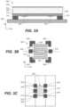
- FIG. 1 Ais a diagram illustrating a side view cross-section (indicated at line 102 of FIG. 1 B ) of an ultrasonic transducer device 100 with four corner anchors 105 and an inner anchor 110 and with two patterned electrodes 122 and 124 placed at the bottom surface of the piezoelectric layer 114 , according to some embodiments.
- ultrasonic transducer device 100is a piezoelectric micromachined ultrasonic transducer (PMUT) device.
- Ultrasonic transducer device 100is one ultrasonic transducer of a two-dimensional array of ultrasonic transducer devices 100 , where each ultrasonic transducer includes a pair of electrodes 122 and 124 .
- Corner anchors 105are positioned at a corner of ultrasonic transducer device 100 and inner anchor 110 is positioned inside of ultrasonic transducer device 100 . It should be appreciated that corner anchors 105 are shared by adjacent ultrasonic transducer devices 100 (e.g., four ultrasonic transducer devices 100 share one corner anchor 105 ) and that inner anchor 110 is dedicated to one ultrasonic transducer device 100 .
- Ultrasonic transducer device 100includes a membrane 108 overlying and attached to four corner anchors 105 and an inner anchor 110 . It should be appreciated that membrane 108 spans all ultrasonic transducer devices 100 of the two-dimensional array of ultrasonic transducer devices 100 .
- Corner anchors 105 and inner anchor 110may be made of electrically conducting materials, such as and without limitation, aluminum, molybdenum, or titanium.
- corner anchors 105 and inner anchor 110may be made of dielectric materials, such as silicon dioxide, silicon nitride or aluminum oxide that have electrical connections along the sides or in vias through corner anchors 105 and inner anchor 110 , for electrically coupling electrodes 122 , 124 , and/or 126 to electrical wiring in substrate 140 .
- substrate 140may include terminals for electrically coupling electrodes 122 , 124 , and/or 126 to control circuitry.
- substrate 140may include at least one of, and without limitation, silicon or silicon nitride. It should be appreciated that substrate 140 may include electrical wirings and connection, such as aluminum or copper.
- substrate 140includes a CMOS logic wafer bonded to corner anchors 105 and inner anchor 110 .
- Membrane 108includes a piezoelectric layer 114 and electrodes 122 , 124 , and 126 , with electrodes 122 and 124 on the same side of piezoelectric layer 114 and electrodes 126 on the opposite side of piezoelectric layer 114 than electrodes 122 and 124 .
- membrane 108further includes structural layer 112 (e.g., a stiffening layer or a mechanical support layer) to mechanically stiffen membrane 108 .
- structural layer 112may include at least one of, and without limitation, silicon, silicon oxide, silicon nitride, aluminum, molybdenum, titanium, etc.
- membrane 108also includes ground electrode 130 placed at the opposite side of the cavity.
- membrane 108can also include other layers (not shown), such as an acoustic coupling layer.
- the acoustic coupling layeris for supporting transmission of acoustic signals, and, if present, is above membrane 108 . It should be appreciated that acoustic coupling layer can include air, liquid, gel-like materials, or other materials for supporting transmission of acoustic signals.
- FIG. 1 Bis a diagram illustrating a top view of the electrode layout of an ultrasonic transducer device 100 with four corner anchors 105 and an inner anchor 110 and with two patterned electrodes 122 and 124 placed at the bottom surface of the piezoelectric layer 114 , according to some embodiments.
- one corner anchor 105is connected to an electric connector 132 for connecting to electrode 122 to an electrical potential
- inner anchor 110is connected to an electric connector 134 for connecting to electrode 124 to an electrical potential.
- a plurality of ultrasonic transducer devices 100are comprised within a two-dimensional (or one-dimensional) array of ultrasonic transducer devices 100 .
- FIG. 1 Cis a diagram illustrating a top view of the anchor configuration of a two-dimensional array of ultrasonic transducer devices 100 with four corner anchors 105 and an inner anchor 110 per ultrasonic transducer device 100 , according to some embodiments. It should be appreciated that FIG. 1 C shows the anchor configuration for one ultrasonic transducer device 100 surrounded by other ultrasonic transducer devices 100 for which the anchor configuration is not shown apart from sharing corner anchors 105 .
- the array of ultrasonic transducer devices 100may be coupled to a platen layer above an acoustic coupling layer for containing the acoustic coupling layer and providing a contact surface for a finger or other sensed object with the array of ultrasonic transducer devices 100 .
- the acoustic coupling layerprovides a contact surface, such that a platen layer is optional.
- the contact surfacecan be flat or of a varying thickness (e.g., curved).
- ultrasonic transducer device 100comprises electrodes 122 , 124 , and 126 that supply and/or collect the electrical charge to/from piezoelectric layer 114 .
- Electrodes 122 , 124 , and 126can be connected to substrate 140 or the underlying circuitry via one or more terminals on substrate 140 .
- ground electrode 130can be connected to substrate 140 or the underlying circuitry via one or more terminals on substrate 140 .
- one corner anchor 105is connected to an electric connector 132 for connecting to electrode 122 to an electrical potential and inner anchor 110 is connected to an electric connector 134 for connecting to electrode 124 to an electrical potential.
- two or more electrodesmay share a single terminal.
- electrodes 122 and 124are patterned electrodes (e.g., a patterned layer).
- electrodes 122 , 124 , 126 , and 130can be comprised of almost any metal layers, such as, but not limited to, aluminum (Al), titanium (Ti), Molybdenum (Mo), etc.
- electrodes 122 , 124 , and/or 126can be patterned in particular shapes (e.g., ring, circle, square, octagon, hexagon, etc.) that are coupled with the membrane 108 .
- electrodes 122 and 124are coupled to different terminals and operate as separate electrodes, where electrode 126 is coupled to ground (GND) or other potential.
- electrodes 130 and 126are coupled to ground (GND).
- electrode 122is dedicated for use in a transmit operation for generating an ultrasonic signal and electrode 124 is dedicated for use in a receive operation for receiving a reflected ultrasonic signal.
- FIG. 2 Ais a diagram illustrating a side view cross-section (indicated at line 202 of FIG. 2 B ) of an ultrasonic transducer device 200 with two side anchors 215 and an inner anchor 210 and with two patterned electrodes 222 and 224 placed at the bottom surface of the piezoelectric layer 214 , according to some embodiments.
- ultrasonic transducer device 200is a PMUT device.
- Ultrasonic transducer device 200is one ultrasonic transducer of a two-dimensional array of ultrasonic transducer devices 200 , where each ultrasonic transducer includes a pair of electrodes 222 and 224 .
- Side anchors 215are positioned at a side of ultrasonic transducer device 200 and inner anchor 210 is positioned inside of ultrasonic transducer device 200 . It should be appreciated that side anchors 215 are shared by adjacent ultrasonic transducer devices 200 (e.g., two ultrasonic transducer devices 200 share one side anchor 215 ) and that inner anchor 210 is dedicated to one ultrasonic transducer device 200 .
- Ultrasonic transducer device 200includes a membrane 208 overlying and attached to two side anchors 215 and an inner anchor 210 . It should be appreciated that membrane 208 spans all ultrasonic transducer devices 200 of the two-dimensional array of ultrasonic transducer devices 200 .
- Side anchors 215 and inner anchor 210may be made of electrically conducting materials, such as and without limitation, aluminum, molybdenum, or titanium.
- side anchors 215 and inner anchor 210may be made of dielectric materials, such as silicon dioxide, silicon nitride or aluminum oxide that have electrical connections along the sides or in vias through side anchors 215 and inner anchor 210 , for electrically coupling electrodes 222 , 224 , and/or 226 to electrical wiring in substrate 240 .
- substrate 240may include terminals for electrically coupling electrodes 222 , 224 , and/or 226 to control circuitry.
- substrate 240may include at least one of, and without limitation, silicon or silicon nitride. It should be appreciated that substrate 240 may include electrical wirings and connection, such as aluminum or copper.
- substrate 240includes a CMOS logic wafer bonded to side anchors 215 and an inner anchor 210 .
- Membrane 208includes piezoelectric layer 214 and electrodes 222 , 224 , and 226 , with electrodes 222 and 224 on the same side of piezoelectric layer 214 and electrodes 226 on the opposite side of piezoelectric layer 214 than electrodes 222 and 224 .
- membrane 208further comprises electrode 230 connected to ground.
- membrane 208further includes structural layer 212 (e.g., a stiffening layer or a mechanical support layer) to mechanically stiffen membrane 208 .
- structural layer 212may include at least one of, and without limitation, silicon, silicon oxide, silicon nitride, aluminum, molybdenum, titanium, etc.
- membrane 208can also include other layers (not shown), such as an acoustic coupling layer.
- the acoustic coupling layeris for supporting transmission of acoustic signals, and, if present, is above membrane 208 .
- acoustic coupling layercan include air, liquid, gel-like materials, or other materials for supporting transmission of acoustic signals.
- FIG. 2 Bis a diagram illustrating a top view of the electrode layout of an ultrasonic transducer device 200 with two side anchors 215 and an inner anchor 210 and with two patterned electrodes 222 and 224 placed at the bottom surface of the piezoelectric layer 214 , according to some embodiments.
- one side anchor 215is connected to an electric connector 232 for connecting to electrode 222 to an electrical potential
- inner anchor 210is connected to an electric connector 234 for connecting to electrode 224 to an electrical potential.
- a plurality of ultrasonic transducer devices 200are comprised within a two-dimensional (or one-dimensional) array of ultrasonic transducer devices 200 .
- FIG. 2 Cis a diagram illustrating a top view of the anchor configuration of a two-dimensional array of ultrasonic transducer devices 200 with two side anchors 215 and an inner anchor 210 per ultrasonic transducer device 200 , according to some embodiments. It should be appreciated that FIG. 2 C shows the anchor configuration for one ultrasonic transducer device 200 surrounded by other ultrasonic transducer devices 200 for which the anchor configuration is not shown apart from sharing side anchors 215 .
- the array of ultrasonic transducer devices 200may be coupled to a platen layer above an acoustic coupling layer for containing the acoustic coupling layer and providing a contact surface for a finger or other sensed object with the array of ultrasonic transducer devices 200 .
- the acoustic coupling layerprovides a contact surface, such that a platen layer is optional.
- the contact surfacecan be flat or of a varying thickness (e.g., curved).
- ultrasonic transducer device 200comprises electrodes 222 , 224 , and 226 that supply and/or collect the electrical charge to/from piezoelectric layer 214 .
- Electrodes 222 , 224 , and 226can be connected to substrate 240 or the underlying circuitry via one or more terminals on substrate 240 .
- ground electrode 230can be connected to substrate 240 or the underlying circuitry via one or more terminals on substrate 240 .
- one side anchor 215is connected to an electric connector 232 for connecting to electrode 222 to an electrical potential and inner anchor 210 is connected to an electric connector 234 for connecting to electrode 224 to an electrical potential.
- two or more electrodesmay share a single terminal.
- electrodes 222 and 224are patterned electrodes (e.g., a patterned layer).
- electrodes 222 , 224 , 226 , and 230can be comprised of almost any metal layers, such as, but not limited to, aluminum (Al), titanium (Ti), Molybdenum (Mo), etc.
- electrodes 222 , 224 , and/or 226can be patterned in particular shapes (e.g., ring, circle, square, octagon, hexagon, etc.) that are coupled with the membrane 208 .
- electrodes 222 and 224are coupled to different terminals and operate as separate electrodes, where electrode 226 is coupled to ground (GND) or other potential.
- electrodes 230 and 226are coupled to ground (GND).
- electrode 222is dedicated for use in a transmit operation for generating an ultrasonic signal and electrode 224 is dedicated for use in a receive operation for receiving a reflected ultrasonic signal.
- FIG. 3 Ais a diagram illustrating a side view cross-section (indicated at line 302 of FIG. 3 B ) of an ultrasonic transducer device 300 with two side anchors 315 and four corner anchors 305 (illustrated in FIG. 3 B ), and with two patterned electrodes 322 and 324 placed at the bottom surface of the piezoelectric layer 314 , according to some embodiments.
- ultrasonic transducer device 300is a PMUT device.
- Ultrasonic transduce device 300is one ultrasonic transducer of a two-dimensional array of ultrasonic transducer devices 300 , where each ultrasonic transducer includes a pair of electrodes 322 and 324 .
- Side anchors 315are positioned at a side of ultrasonic transducer device 300 and corner anchors 305 are positioned at a corner of ultrasonic transducer device 300 . It should be appreciated that side anchors 315 and corner anchors 305 are shared by adjacent ultrasonic transducer devices 300 (e.g., two ultrasonic transducer devices 300 share one side anchor 315 and four ultrasonic transducer devices 300 share one corner anchor 305 ).
- Ultrasonic transducer device 300includes a membrane 308 overlying and attached to two side anchors 315 and four corner anchors 305 . It should be appreciated that membrane 308 spans all ultrasonic transducer devices 300 of the two-dimensional array of ultrasonic transducer devices 300 . Side anchors 315 and corner anchors 305 may be made of electrically conducting materials, such as and without limitation, aluminum, molybdenum, or titanium.
- side anchors 315 and corner anchors 305may be made of dielectric materials, such as silicon dioxide, silicon nitride or aluminum oxide that have electrical connections along the sides or in vias through side anchors 315 and corner anchors 305 , for electrically coupling electrodes 322 , 324 , and/or 326 to electrical wiring in substrate 340 .
- substrate 340may include terminals for electrically coupling electrodes 322 , 324 , and/or 326 to control circuitry.
- substrate 340may include at least one of, and without limitation, silicon or silicon nitride. It should be appreciated that substrate 340 may include electrical wirings and connection, such as aluminum or copper.
- substrate 340includes a CMOS logic wafer bonded to side anchors 315 and corner anchors 305 .
- Membrane 308includes a piezoelectric layer 314 and electrodes 322 , 324 , and 326 , with electrodes 322 and 324 on the same side of piezoelectric layer 314 and electrodes 326 on the opposite side of piezoelectric layer 314 than electrodes 322 and 324 .
- membrane 308further includes electrode 330 connected to ground.
- membrane 308further includes structural layer 312 (e.g., a stiffening layer or a mechanical support layer) to mechanically stiffen membrane 308 .
- structural layer 312may include at least one of, and without limitation, silicon, silicon oxide, silicon nitride, aluminum, molybdenum, titanium, etc.
- membrane 308can also include other layers (not shown), such as an acoustic coupling layer.
- the acoustic coupling layeris for supporting transmission of acoustic signals, and, if present, is above membrane 308 .
- acoustic coupling layercan include air, liquid, gel-like materials, or other materials for supporting transmission of acoustic signals.
- FIG. 3 Bis a diagram illustrating a top view of the electrode layout of an ultrasonic transducer device 300 with two side anchors 315 and four corner anchors 305 and with two patterned electrodes 322 and 324 placed at the bottom surface of the piezoelectric layer 314 , according to some embodiments.
- one side anchor 315is connected to an electric connector 334 for connecting to electrode 324 to an electrical potential
- one corner anchor 305is connected to an electric connector 332 for connecting to electrode 322 to an electrical potential.
- a plurality of ultrasonic transducer devices 300are comprised within a two-dimensional (or one-dimensional) array of ultrasonic transducer devices 300 .
- FIG. 3 Cis a diagram illustrating a top view of the anchor configuration of a two-dimensional array of ultrasonic transducer devices 300 with two side anchors 315 and four corner anchors 305 per ultrasonic transducer device 300 , according to some embodiments. It should be appreciated that FIG. 3 C shows the anchor configuration for one ultrasonic transducer device 300 surrounded by other ultrasonic transducer devices 300 for which the anchor configuration is not shown apart from sharing side anchors 315 and corner anchors 305 .
- the array of ultrasonic transducer devices 300may be coupled to a platen layer above an acoustic coupling layer for containing the acoustic coupling layer and providing a contact surface for a finger or other sensed object with the array of ultrasonic transducer devices 300 .
- the acoustic coupling layerprovides a contact surface, such that a platen layer is optional. It should be appreciated that the contact surface can be flat or of a varying thickness (e.g., curved).
- ultrasonic transducer device 300comprises electrodes 322 , 324 , and 326 that supply and/or collect the electrical charge to/from piezoelectric layer 314 .
- Electrodes 322 , 324 , and 326can be connected to substrate 340 or the underlying circuitry via one or more terminals on substrate 340 .
- ground electrode 330can be connected to substrate 340 or the underlying circuitry via one or more terminals on substrate 340 .
- one side anchor 315is connected to an electric connector 334 for connecting to electrode 324 to an electrical potential and one corner anchor 305 is connected to an electric connector 332 for connecting to electrode 322 to an electrical potential.
- two or more electrodesmay share a single terminal.
- electrodes 322 and 324are patterned electrodes (e.g., a patterned layer).
- electrodes 322 , 324 , 326 , and 330can be comprised of almost any metal layers, such as, but not limited to, aluminum (Al), titanium (Ti), Molybdenum (Mo), etc.
- electrodes 322 , 324 , and/or 326can be patterned in particular shapes (e.g., ring, circle, square, octagon, hexagon, etc.) that are coupled with the membrane 308 .
- electrodes 322 and 324are coupled to different terminals and operate as separate electrodes, where electrode 326 is coupled to ground (GND) or other potential.
- electrodes 330 and 326are coupled to ground (GND).
- electrode 322is dedicated for use in a transmit operation for generating an ultrasonic signal and electrode 324 is dedicated for use in a receive operation for receiving a reflected ultrasonic signal.
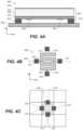
- FIG. 4 Ais a diagram illustrating a side view cross-section (indicated at line 402 of FIG. 4 B ) of an ultrasonic transducer device 400 with four side anchors 415 and with two patterned electrodes 422 and 424 placed at the bottom surface of the piezoelectric layer 414 , according to some embodiments.
- ultrasonic transducer device 400is a PMUT device.
- Ultrasonic transducer device 400is one ultrasonic transducer of a two-dimensional array of ultrasonic transducer devices 400 , where each ultrasonic transducer includes a pair of electrodes 422 and 424 .
- Side anchors 415are positioned at a side of ultrasonic transducer device 400 . It should be appreciated that side anchors 415 are shared by adjacent ultrasonic transducer devices 400 (e.g., two ultrasonic transducer devices 400 share one side anchor 415 ).
- Ultrasonic transducer device 400includes a membrane 408 overlying and attached to four side anchors 415 . It should be appreciated that membrane 408 spans all ultrasonic transducer devices 400 of the two-dimensional array of ultrasonic transducer devices 400 .
- Side anchors 415may be made of electrically conducting materials, such as and without limitation, aluminum, molybdenum, or titanium.
- side anchors 415may be made of dielectric materials, such as silicon dioxide, silicon nitride or aluminum oxide that have electrical connections along the sides or in vias through side anchors 415 , for electrically coupling electrodes 422 , 424 , and/or 426 to electrical wiring in substrate 440 .
- substrate 440may include terminals for electrically coupling electrodes 422 , 424 , and/or 426 to control circuitry.
- substrate 440may include at least one of, and without limitation, silicon or silicon nitride. It should be appreciated that substrate 440 may include electrical wirings and connection, such as aluminum or copper.
- substrate 440includes a CMOS logic wafer bonded to side anchors 415 .
- Membrane 408includes piezoelectric layer 414 and electrodes 422 , 424 , and 426 , with electrodes 422 and 424 on the same side of piezoelectric layer 414 and electrodes 426 on the opposite side of piezoelectric layer 414 than electrodes 422 and 424 .
- membrane 308further includes electrode 430 connected to ground.
- membrane 408further includes structural layer 412 (e.g., a stiffening layer or a mechanical support layer) to mechanically stiffen membrane 408 .
- structural layer 412may include at least one of, and without limitation, silicon, silicon oxide, silicon nitride, aluminum, molybdenum, titanium, etc.
- membrane 408can also include other layers (not shown), such as an acoustic coupling layer.
- the acoustic coupling layeris for supporting transmission of acoustic signals, and, if present, is above membrane 408 .
- acoustic coupling layercan include air, liquid, gel-like materials, or other materials for supporting transmission of acoustic signals.
- FIG. 4 Bis a diagram illustrating a top view of the electrode layout of an ultrasonic transducer device 400 with four side anchors 415 and with two patterned electrodes 422 and 424 placed at the bottom surface of the piezoelectric layer 414 , according to some embodiments.
- one side anchor 415is connected to an electric connector 432 for connecting to electrode 422 to an electrical potential and another side anchor 415 is connected to an electric connector 434 for connecting to electrode 424 to an electrical potential.
- a plurality of ultrasonic transducer devices 400are comprised within a two-dimensional (or one-dimensional) array of ultrasonic transducer devices 400 .
- FIG. 4 Cis a diagram illustrating a top view of the anchor configuration of a two-dimensional array of ultrasonic transducer devices 400 with four side anchors 415 per ultrasonic transducer device 400 , according to some embodiments. It should be appreciated that FIG. 4 C shows the anchor configuration for one ultrasonic transducer device 400 surrounded by other ultrasonic transducer devices 400 for which the anchor configuration is not shown apart from sharing side anchors 415 .
- the array of ultrasonic transducer devices 400may be coupled to a platen layer above an acoustic coupling layer for containing the acoustic coupling layer and providing a contact surface for a finger or other sensed object with the array of ultrasonic transducer devices 400 .
- the acoustic coupling layerprovides a contact surface, such that a platen layer is optional. It should be appreciated that the contact surface can be flat or of a varying thickness (e.g., curved).
- ultrasonic transducer device 400comprises electrodes 422 , 424 , and 426 that supply and/or collect the electrical charge to/from piezoelectric layer 414 .
- Electrodes 422 , 424 , and 426can be connected to substrate 440 or the underlying circuitry via one or more terminals on substrate 440 .
- ground electrode 430can be connected to substrate 440 or the underlying circuitry via one or more terminals on substrate 440 .
- one side anchor 415is connected to an electric connector 432 for connecting to electrode 422 to an electrical potential and another side anchor 415 is connected to an electric connector 434 for connecting to electrode 424 to an electrical potential.
- two or more electrodesmay share a single terminal.
- electrodes 422 and 424are patterned electrodes (e.g., a patterned layer).
- electrodes 422 , 424 , 426 , and 430can be comprised of almost any metal layers, such as, but not limited to, aluminum (Al), titanium (Ti), Molybdenum (Mo), etc.
- electrodes 422 , 424 , and/or 426can be patterned in particular shapes (e.g., ring, circle, square, octagon, hexagon, etc.) that are coupled with the membrane 408 .
- electrodes 422 and 424are coupled to different terminals and operate as separate electrodes, where electrode 426 is coupled to ground (GND) or other potential.
- electrodes 430 and 426are coupled to ground (GND).
- electrode 422is dedicated for use in a transmit operation for generating an ultrasonic signal and electrode 424 is dedicated for use in a receive operation for receiving a reflected ultrasonic signal.
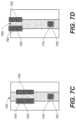
- FIG. 5 Ais a diagram illustrating a side view cross-section (indicated at line 502 of FIG. 5 B ) of an ultrasonic transducer device 500 with two inner anchors 510 and with two patterned electrodes 522 and 524 placed at the bottom surface of the piezoelectric layer 514 , according to some embodiments.
- ultrasonic transducer device 500is a PMUT device.
- Ultrasonic transducer device 500is one ultrasonic transducer of a two-dimensional array of ultrasonic transducer devices 500 , where each ultrasonic transducer includes a pair of electrodes 522 and 524 .
- Inner anchors 510are positioned inside of ultrasonic transducer device 500 . It should be appreciated that inner anchors 510 are dedicated to ultrasonic transducer device 500 and are not shared by any adjacent ultrasonic transducer device 500 .
- Ultrasonic transducer device 500includes a membrane 508 overlying and attached to two inner anchors 510 . It should be appreciated that membrane 508 spans all ultrasonic transducer devices 500 of the two-dimensional array of ultrasonic transducer devices 500 .
- Inner anchors 510may be made of electrically conducting materials, such as and without limitation, aluminum, molybdenum, or titanium.
- inner anchors 510may be made of dielectric materials, such as silicon dioxide, silicon nitride or aluminum oxide that have electrical connections along the sides or in vias through inner anchors 510 , for electrically coupling electrodes 522 , 524 , and/or 526 to electrical wiring in substrate 540 .
- substrate 540may include terminals for electrically coupling electrodes 522 , 524 , and/or 526 to control circuitry.
- substrate 540may include at least one of, and without limitation, silicon or silicon nitride. It should be appreciated that substrate 540 may include electrical wirings and connection, such as aluminum or copper.
- substrate 540includes a CMOS logic wafer bonded to inner anchors 510 .
- Membrane 508includes a piezoelectric layer 514 and electrodes 522 , 524 , and 526 , with electrodes 522 and 524 on the same side of piezoelectric layer 514 and electrodes 526 on the opposite side of piezoelectric layer 514 than electrodes 522 and 524 .
- membrane 308further includes electrode 530 connected to ground.
- membrane 508further includes a structural layer 512 (e.g., a stiffening layer or a mechanical support layer) to mechanically stiffen membrane 508 .
- structural layer 512may include at least one of, and without limitation, silicon, silicon oxide, silicon nitride, aluminum, molybdenum, titanium, etc.
- membrane 508can also include other layers (not shown), such as an acoustic coupling layer.
- the acoustic coupling layeris for supporting transmission of acoustic signals, and, if present, is above membrane 508 .
- acoustic coupling layercan include air, liquid, gel-like materials, or other materials for supporting transmission of acoustic signals.
- FIG. 5 Bis a diagram illustrating a top view of the electrode layout of an ultrasonic transducer device 500 with two inner anchors 510 and with two patterned electrodes 522 and 524 placed at the bottom surface of the piezoelectric layer 514 , according to some embodiments.
- one inner anchor 510is connected to an electric connector 532 for connecting to electrode 522 to an electrical potential and another inner anchor 510 is connected to an electric connector 534 for connecting to electrode 524 to an electrical potential.
- a plurality of ultrasonic transducer devices 500are comprised within a two-dimensional (or one-dimensional) array of ultrasonic transducer devices 500 .
- FIG. 5 Cis a diagram illustrating a top view of the anchor configuration of a two-dimensional array of ultrasonic transducer devices 500 with two inner anchors 510 per ultrasonic transducer device 500 , according to some embodiments. It should be appreciated that FIG. 5 C shows the anchor configuration for one ultrasonic transducer device 500 surrounded by other ultrasonic transducer devices 500 for which the anchor configuration is not shown.
- the array of ultrasonic transducer devices 500may be coupled to a platen layer above an acoustic coupling layer for containing the acoustic coupling layer and providing a contact surface for a finger or other sensed object with the array of ultrasonic transducer devices 500 .
- the acoustic coupling layerprovides a contact surface, such that a platen layer is optional. It should be appreciated that the contact surface can be flat or of a varying thickness (e.g., curved).
- ultrasonic transducer device 500comprises electrodes 522 , 524 , and 526 that supply and/or collect the electrical charge to/from piezoelectric layer 514 .
- Electrodes 522 , 524 , and 526can be connected to substrate 540 or the underlying circuitry via one or more terminals on substrate 540 .
- ground electrode 530can be connected to substrate 540 or the underlying circuitry via one or more terminals on substrate 540 .
- one inner anchor 510is connected to an electric connector 532 for connecting to electrode 522 to an electrical potential and another inner anchor 510 is connected to an electric connector 534 for connecting to electrode 524 to an electrical potential.
- two or more electrodesmay share a single terminal.
- electrodes 522 and 524are patterned electrodes (e.g., a patterned layer).
- electrodes 522 , 524 , 526 , and 530can be comprised of almost any metal layers, such as, but not limited to, aluminum (Al), titanium (Ti), Molybdenum (Mo), etc.
- electrodes 522 , 524 , and/or 526can be patterned in particular shapes (e.g., ring, circle, square, octagon, hexagon, etc.) that are coupled with the membrane 508 .
- electrodes 522 and 524are coupled to different terminals and operate as separate electrodes, where electrode 526 is coupled to ground (GND) or other potential.
- electrodes 530 and 526are coupled to ground (GND).
- electrode 522is dedicated for use in a transmit operation for generating an ultrasonic signal and electrode 524 is dedicated for use in a receive operation for receiving a reflected ultrasonic signal.
- a plurality of ultrasonic transducer devicesis comprised within a one-dimensional array of ultrasonic transducer devices.
- FIGS. 6 A through 8 Cillustrates different anchor configurations of example one-dimensional arrays of ultrasonic transducer devices. It should be appreciated that the ultrasonic transducer devices of FIGS. 6 A through 8 C operate in a similar manner and include the same componentry as the ultrasonic transducer devices of FIGS. 1 A through 5 C (e.g., ultrasonic transducer devices 100 , 200 , 300 , 400 , and 500 ) with the exception of their use only within a one-dimensional array of ultrasonic transducer devices. As such, the ultrasonic transducer devices of FIGS.
- 6 A through 8 Ceach have two shared sides (e.g., sides adjacent to another ultrasonic transducer device) and exclusive sides (e.g., sides not adjacent to another ultrasonic transducer device), with the exception of ultrasonic transducer devices at the ends of the one-dimensional array having one shared side and three exclusive sides.
- the ultrasonic transducer devices of FIGS. 6 A through 8 Cemploy a piezoelectric layer comprised of materials such as, but not limited to, aluminum nitride (AlN), scandium doped aluminum nitride (ScAlN), lead zirconate titanate (PZT), quartz, polyvinylidene fluoride (PVDF), and/or zinc oxide, to facilitate both acoustic signal production (transmitting) and sensing (receiving).
- the piezoelectric layercan generate electric charges under mechanical stress and conversely experience a mechanical strain in the presence of an electric field.
- the piezoelectric layercan sense mechanical vibrations caused by an ultrasonic signal and produce an electrical charge at the frequency (e.g., ultrasonic frequency) of the vibrations. Additionally, the piezoelectric layer can generate an ultrasonic wave by vibrating in an oscillatory fashion that might be at the same frequency (e.g., ultrasonic frequency) as an input current generated by an alternating current (AC) voltage applied across the piezoelectric layer.
- ACalternating current
- piezoelectric layercan include almost any material (or combination of materials) that exhibits piezoelectric properties. The polarization is directly proportional to the applied stress and is direction dependent so that compressive and tensile stresses results in electric fields of opposite polarizations.
- FIG. 6 Ais a diagram illustrating a top view of the anchor configuration of a one-dimensional array of ultrasonic transducer devices 600 with four shared side anchors 605 , according to some embodiments. It should be appreciated that FIG. 6 A shows the anchor configuration for one ultrasonic transducer device 600 surrounded by two other ultrasonic transducer devices 600 on each shared side for which the anchor configuration is not shown, apart from the shared side anchors 605 .
- ultrasonic transducer device 600is a PMUT device.
- Ultrasonic transducer device 600is one ultrasonic transducer of a one-dimensional array of ultrasonic transducer devices 600 , where each ultrasonic transducer includes a pair of electrodes to which electrical connections 632 and 634 are electrically coupled.
- the electrodescan be connected to a substrate or the underlying circuitry via one or more terminals on the substrate.
- ultrasonic transducer device 600has four shared side anchors 605 , where a shared side anchor 605 is on a shared side of ultrasonic transducer device 600 .
- Electrical connection 632is for connecting one electrode to an electrical potential and electrical connection 634 is for connecting another electrode to an electrical potential.
- the electrodesare patterned electrodes (e.g., a patterned layer).
- the electrodescan be comprised of almost any metal layers, such as, but not limited to, aluminum (Al), titanium (Ti), Molybdenum (Mo), etc.
- Ultrasonic transducer device 600includes a membrane overlying and attached to shared side anchors 605 . It should be appreciated that the membrane spans all ultrasonic transducer devices 600 of the one-dimensional array of ultrasonic transducer devices 600 .
- Shared side anchors 605may be made of electrically conducting materials, such as and without limitation, aluminum, molybdenum, or titanium.
- shared side anchors 605may be made of dielectric materials, such as silicon dioxide, silicon nitride or aluminum oxide that have electrical connections 632 and 634 along the sides or in vias through shared side anchors 605 , for electrically coupling electrodes to electrical wiring in the substrate.
- the substratemay include terminals for electrically coupling the electrodes to control circuitry.
- Ultrasonic transducer device 600comprises electrodes that supply and/or collect the electrical charge to/from the piezoelectric layer.
- one shared side anchor 605is connected to an electrical connection 632 for connecting one electrode to an electrical potential and another shared side anchor 605 is connected to an electrical connection 634 for connecting another electrode to an electrical potential.
- the electrodescan be patterned in particular shapes (e.g., ring, circle, square, octagon, hexagon, etc.) that are coupled with the membrane.
- the electrodesare coupled to different terminals and operate as separate electrodes.
- the electrode coupled to electrical connection 632is dedicated for use in a transmit operation for generating an ultrasonic signal and the electrode coupled to electrical connection 634 is dedicated for use in a receive operation for receiving a reflected ultrasonic signal.
- FIG. 6 Bis a diagram illustrating a top view of the anchor configuration of a one-dimensional array of ultrasonic transducer devices 630 with two shared side anchors 635 and two corner anchors 645 , according to some embodiments. It should be appreciated that FIG. 6 B shows the anchor configuration for one ultrasonic transducer device 630 surrounded by two other ultrasonic transducer devices 630 on each shared side for which the anchor configuration is not shown, apart from the shared side anchors 635 and the corner anchors 645 .
- ultrasonic transducer device 630is a PMUT device.
- Ultrasonic transducer device 630is one ultrasonic transducer of a one-dimensional array of ultrasonic transducer devices 630 , where each ultrasonic transducer includes a pair of electrodes to which electrical connections 662 and 664 are electrically coupled. The electrodes can be connected to a substrate or the underlying circuitry via one or more terminals on the substrate.
- ultrasonic transducer device 630has two shared side anchors 635 , where a side anchor 635 is on a shared side of ultrasonic transducer device 630 , and two corner anchors 645 , where a corner anchor is both on a shared side and on exclusive side of ultrasonic transducer device 630 .
- Electrode 662is for connecting one electrode to an electrical potential and electrical connection 664 is for connecting another electrode to an electrical potential.
- the electrodesare patterned electrodes (e.g., a patterned layer).
- the electrodescan be comprised of almost any metal layers, such as, but not limited to, aluminum (Al), titanium (Ti), Molybdenum (Mo), etc.
- Ultrasonic transducer device 630includes a membrane overlying and attached to shared side anchors 635 and to corner anchors 645 . It should be appreciated that the membrane spans all ultrasonic transducer devices 630 of the one-dimensional array of ultrasonic transducer devices 630 .
- Shared side anchors 635 and corner anchors 645may be made of electrically conducting materials, such as and without limitation, aluminum, molybdenum, or titanium.
- shared side anchors 635 and corner anchors 645may be made of dielectric materials, such as silicon dioxide, silicon nitride or aluminum oxide that have electrical connections 662 and 664 along the sides or in vias through shared side anchors 635 and corner anchors 645 , for electrically coupling electrodes to electrical wiring in the substrate.
- the substratemay include terminals for electrically coupling the electrodes to control circuitry.
- Ultrasonic transducer device 630comprises electrodes that supply and/or collect the electrical charge to/from the piezoelectric layer.
- one shared side anchor 635is connected to an electrical connection 664 for connecting one electrode to an electrical potential and one corner anchor 645 is connected to an electrical connection 662 for connecting another electrode to an electrical potential.
- the electrodescan be patterned in particular shapes (e.g., ring, circle, square, octagon, hexagon, etc.) that are coupled with the membrane.
- the electrodesare coupled to different terminals and operate as separate electrodes.
- the electrode coupled to electrical connection 662is dedicated for use in a transmit operation for generating an ultrasonic signal and the electrode coupled to electrical connection 664 is dedicated for use in a receive operation for receiving a reflected ultrasonic signal.
- FIG. 6 Cis a diagram illustrating a top view of the anchor configuration of a one-dimensional array of ultrasonic transducer devices 660 with four corner anchors 675 , according to some embodiments. It should be appreciated that FIG. 6 C shows the anchor configuration for one ultrasonic transducer device 660 surrounded by two other ultrasonic transducer devices 660 on each shared side for which the anchor configuration is not shown, apart from the corner anchors 675 .
- ultrasonic transducer device 660is a PMUT device.
- Ultrasonic transducer device 660is one ultrasonic transducer of a one-dimensional array of ultrasonic transducer devices 660 , where each ultrasonic transducer includes a pair of electrodes to which electrical connections 692 and 694 are electrically coupled.
- the electrodescan be connected to a substrate or the underlying circuitry via one or more terminals on the substrate.
- ultrasonic transducer device 660has four corner anchors 675 , where a corner anchor 675 is on both a shared side and an exclusive side of ultrasonic transducer device 660 .
- Electrical connection 692is for connecting one electrode to an electrical potential and electrical connection 694 is for connecting another electrode to an electrical potential.
- the electrodesare patterned electrodes (e.g., a patterned layer).
- the electrodescan be comprised of almost any metal layers, such as, but not limited to, aluminum (Al), titanium (Ti), Molybdenum (Mo), etc.
- Ultrasonic transducer device 660includes a membrane overlying and attached to corner anchors 675 . It should be appreciated that the membrane spans all ultrasonic transducer devices 660 of the one-dimensional array of ultrasonic transducer devices 660 .
- Corner anchors 675may be made of electrically conducting materials, such as and without limitation, aluminum, molybdenum, or titanium.
- corner anchors 675may be made of dielectric materials, such as silicon dioxide, silicon nitride or aluminum oxide that have electrical connections 692 and 694 along the sides or in vias through corner anchors 675 , for electrically coupling electrodes to electrical wiring in the substrate.
- the substratemay include terminals for electrically coupling the electrodes to control circuitry.
- Ultrasonic transducer device 660comprises electrodes that supply and/or collect the electrical charge to/from the piezoelectric layer.
- one corner anchor 675is connected to an electrical connection 692 for connecting one electrode to an electrical potential and another corner anchor 675 is connected to an electrical connection 694 for connecting another electrode to an electrical potential.
- the electrodescan be patterned in particular shapes (e.g., ring, circle, square, octagon, hexagon, etc.) that are coupled with the membrane.
- the electrodesare coupled to different terminals and operate as separate electrodes.
- the electrode coupled to electrical connection 692is dedicated for use in a transmit operation for generating an ultrasonic signal and the electrode coupled to electrical connection 694 is dedicated for use in a receive operation for receiving a reflected ultrasonic signal.
- FIG. 7 Ais a diagram illustrating a top view of the anchor configuration of a one-dimensional array of ultrasonic transducer devices 700 with two shared side anchors 705 and one exclusive side anchor 715 , according to some embodiments. It should be appreciated that FIG. 7 A shows the anchor configuration for one ultrasonic transducer device 700 surrounded by two other ultrasonic transducer devices 700 on each shared side for which the anchor configuration is not shown, apart from the shared side anchors 705 . In some embodiments, ultrasonic transducer device 700 is a PMUT device.
- Ultrasonic transducer device 700is one ultrasonic transducer of a one-dimensional array of ultrasonic transducer devices 700 , where each ultrasonic transducer includes a pair of electrodes to which electrical connections 722 and 724 are electrically coupled.
- the electrodescan be connected to a substrate or the underlying circuitry via one or more terminals on the substrate.
- ultrasonic transducer device 700has two shared side anchors 705 and one excusive side anchor 715 , where a shared side anchor 705 is on a shared side of ultrasonic transducer device 700 and an exclusive side anchor 715 is on an exclusive side of ultrasonic transducer device 700 .
- Electrode 722is for connecting one electrode to an electrical potential and electrical connection 724 is for connecting another electrode to an electrical potential.
- the electrodesare patterned electrodes (e.g., a patterned layer).
- the electrodescan be comprised of almost any metal layers, such as, but not limited to, aluminum (Al), titanium (Ti), Molybdenum (Mo), etc.
- Ultrasonic transducer device 700includes a membrane overlying and attached to shared side anchors 705 and exclusive side anchor 715 . It should be appreciated that the membrane spans all ultrasonic transducer devices 700 of the one-dimensional array of ultrasonic transducer devices 700 .
- Shared side anchors 705 and exclusive side anchor 715may be made of electrically conducting materials, such as and without limitation, aluminum, molybdenum, or titanium.
- shared side anchors 705 and exclusive side anchor 715may be made of dielectric materials, such as silicon dioxide, silicon nitride or aluminum oxide that have electrical connections 722 and 724 along the sides or in vias through shared side anchors 705 and/or exclusive side anchor 715 , for electrically coupling electrodes to electrical wiring in the substrate.
- the substratemay include terminals for electrically coupling the electrodes to control circuitry.
- Ultrasonic transducer device 700comprises electrodes that supply and/or collect the electrical charge to/from the piezoelectric layer.
- exclusive side anchor 715is connected to an electrical connection 722 for connecting one electrode to an electrical potential and one shared side anchor 705 is connected to an electrical connection 724 for connecting another electrode to an electrical potential.
- the electrodescan be patterned in particular shapes (e.g., ring, circle, square, octagon, hexagon, etc.) that are coupled with the membrane.
- the electrodesare coupled to different terminals and operate as separate electrodes.
- the electrode coupled to electrical connection 722is dedicated for use in a transmit operation for generating an ultrasonic signal and the electrode coupled to electrical connection 724 is dedicated for use in a receive operation for receiving a reflected ultrasonic signal.
- FIG. 7 Bis a diagram illustrating a top view of the anchor configuration of a one-dimensional array of ultrasonic transducer devices 720 with two corner anchors 725 and one exclusive side anchor 735 , according to some embodiments. It should be appreciated that FIG. 7 B shows the anchor configuration for one ultrasonic transducer device 720 surrounded by two other ultrasonic transducer devices 720 on each shared side for which the anchor configuration is not shown, apart from the corner anchors 725 .
- ultrasonic transducer device 720is a PMUT device.
- Ultrasonic transducer device 720is one ultrasonic transducer of a one-dimensional array of ultrasonic transducer devices 720 , where each ultrasonic transducer includes a pair of electrodes to which electrical connections 742 and 744 are electrically coupled. The electrodes can be connected to a substrate or the underlying circuitry via one or more terminals on the substrate.
- ultrasonic transducer device 720has two corner anchors 725 and one exclusive side anchor 735 , where a corner anchor 725 is on both a shared side and an exclusive side of ultrasonic transducer device 720 and an exclusive side anchor 735 is on an exclusive side of ultrasonic transducer device 720 .
- Electrode 742is for connecting one electrode to an electrical potential and electrical connection 744 is for connecting another electrode to an electrical potential.
- the electrodesare patterned electrodes (e.g., a patterned layer).
- the electrodescan be comprised of almost any metal layers, such as, but not limited to, aluminum (Al), titanium (Ti), Molybdenum (Mo), etc.
- Ultrasonic transducer device 720includes a membrane overlying and attached to corner anchors 725 and exclusive side anchor 735 . It should be appreciated that the membrane spans all ultrasonic transducer devices 720 of the one-dimensional array of ultrasonic transducer devices 720 .
- Corner anchors 725 and exclusive side anchor 735may be made of electrically conducting materials, such as and without limitation, aluminum, molybdenum, or titanium.
- corner anchors 725 and exclusive side anchor 735may be made of dielectric materials, such as silicon dioxide, silicon nitride or aluminum oxide that have electrical connections 742 and 744 along the sides or in vias through corner anchors 725 and/or exclusive side anchor 735 , for electrically coupling electrodes to electrical wiring in the substrate.
- the substratemay include terminals for electrically coupling the electrodes to control circuitry.
- FIG. 7 Cis a diagram illustrating a top view of the anchor configuration of a one-dimensional array of ultrasonic transducer devices 740 with two shared side anchors 745 and one inner anchor 755 , according to some embodiments. It should be appreciated that FIG. 7 C shows the anchor configuration for one ultrasonic transducer device 740 surrounded by two other ultrasonic transducer devices 740 on each shared side for which the anchor configuration is not shown, apart from the shared side anchors 745 .
- ultrasonic transducer device 740is a PMUT device.
- shared side anchors 745 and inner anchors 755may be made of dielectric materials, such as silicon dioxide, silicon nitride or aluminum oxide that have electrical connections 762 and 764 along the sides or in vias through shared side anchors 745 and/or inner anchors 755 , for electrically coupling electrodes to electrical wiring in the substrate.
- the substratemay include terminals for electrically coupling the electrodes to control circuitry.
- FIG. 7 Dis a diagram illustrating a top view of the anchor configuration of a one-dimensional array of ultrasonic transducer devices 760 with two corner anchors 765 and one inner anchor 775 , according to some embodiments. It should be appreciated that FIG. 7 D shows the anchor configuration for one ultrasonic transducer device 760 surrounded by two other ultrasonic transducer devices 760 on each shared side for which the anchor configuration is not shown, apart from the corner anchors 765 . In some embodiments, ultrasonic transducer device 760 is a PMUT device.
- Ultrasonic transducer device 760is one ultrasonic transducer of a one-dimensional array of ultrasonic transducer devices 760 , where each ultrasonic transducer includes a pair of electrodes to which electrical connections 782 and 784 are electrically coupled. The electrodes can be connected to a substrate or the underlying circuitry via one or more terminals on the substrate.
- ultrasonic transducer device 760has two corner anchors 765 and inner anchor 775 , where a corner anchor 765 is on both a shared side and an exclusive side of ultrasonic transducer device 760 and an inner anchor 775 is positioned inside the ultrasonic transducer device 760 .
- Ultrasonic transducer device 760includes a membrane overlying and attached to corner anchors 765 and inner anchors 775 . It should be appreciated that the membrane spans all ultrasonic transducer devices 760 of the one-dimensional array of ultrasonic transducer devices 760 .
- Corner anchors 765 and inner anchors 775may be made of electrically conducting materials, such as and without limitation, aluminum, molybdenum, or titanium.
- corner anchors 765 and inner anchors 775may be made of dielectric materials, such as silicon dioxide, silicon nitride or aluminum oxide that have electrical connections 782 and 784 along the sides or in vias through corner anchors 765 and/or inner anchors 775 , for electrically coupling electrodes to electrical wiring in the substrate.
- the substratemay include terminals for electrically coupling the electrodes to control circuitry.
- Ultrasonic transducer device 760comprises electrodes that supply and/or collect the electrical charge to/from the piezoelectric layer.
- inner anchor 775is connected to an electrical connection 782 for connecting one electrode to an electrical potential and one corner anchor 765 is connected to an electrical connection 784 for connecting another electrode to an electrical potential.
- the electrodescan be patterned in particular shapes (e.g., ring, circle, square, octagon, hexagon, etc.) that are coupled with the membrane.
- the electrodesare coupled to different terminals and operate as separate electrodes.
- the electrode coupled to electrical connection 782is dedicated for use in a transmit operation for generating an ultrasonic signal and the electrode coupled to electrical connection 784 is dedicated for use in a receive operation for receiving a reflected ultrasonic signal.
- FIG. 8 Ais a diagram illustrating a top view of the anchor configuration of a one-dimensional array of ultrasonic transducer devices 800 with two inner anchors 805 , according to some embodiments. It should be appreciated that FIG. 8 A shows the anchor configuration for one ultrasonic transducer device 800 surrounded by two other ultrasonic transducer devices 800 on each shared side for which the anchor configuration is not shown. In some embodiments, ultrasonic transducer device 800 is a PMUT device.
- Ultrasonic transducer device 800is one ultrasonic transducer of a one-dimensional array of ultrasonic transducer devices 800 , where each ultrasonic transducer includes a pair of electrodes to which electrical connections 832 and 834 are electrically coupled.
- the electrodescan be connected to a substrate or the underlying circuitry via one or more terminals on the substrate.
- ultrasonic transducer device 800has two inner anchors 805 , where an inner anchor 805 is positioned inside the ultrasonic transducer device 800 .
- Electrical connection 832is for connecting one electrode to an electrical potential and electrical connection 834 is for connecting another electrode to an electrical potential.
- the electrodesare patterned electrodes (e.g., a patterned layer).
- the electrodescan be comprised of almost any metal layers, such as, but not limited to, aluminum (Al), titanium (Ti), Molybdenum (Mo), etc.
- Ultrasonic transducer device 800includes a membrane overlying and attached to two inner anchors 805 . It should be appreciated that the membrane spans all ultrasonic transducer devices 800 of the one-dimensional array of ultrasonic transducer devices 800 .
- Inner anchors 805may be made of electrically conducting materials, such as and without limitation, aluminum, molybdenum, or titanium.
- inner anchors 805may be made of dielectric materials, such as silicon dioxide, silicon nitride or aluminum oxide that have electrical connections 832 and 834 along the sides or in vias through inner anchors 805 , for electrically coupling electrodes to electrical wiring in the substrate.
- the substratemay include terminals for electrically coupling the electrodes to control circuitry.
- Ultrasonic transducer device 800comprises electrodes that supply and/or collect the electrical charge to/from the piezoelectric layer.
- one inner anchor 805is connected to an electrical connection 832 for connecting one electrode to an electrical potential and another inner anchor 805 is connected to an electrical connection 834 for connecting another electrode to an electrical potential.
- the electrodescan be patterned in particular shapes (e.g., ring, circle, square, octagon, hexagon, etc.) that are coupled with the membrane.
- the electrodesare coupled to different terminals and operate as separate electrodes.
- the electrode coupled to electrical connection 832is dedicated for use in a transmit operation for generating an ultrasonic signal and the electrode coupled to electrical connection 834 is dedicated for use in a receive operation for receiving a reflected ultrasonic signal.
- FIG. 8 Bis a diagram illustrating a top view of the anchor configuration of a one-dimensional array of ultrasonic transducer devices 830 with two exclusive side anchors 835 , according to some embodiments. It should be appreciated that FIG. 8 B shows the anchor configuration for one ultrasonic transducer device 830 surrounded by two other ultrasonic transducer devices 830 on each shared side for which the anchor configuration is not shown. In some embodiments, ultrasonic transducer device 830 is a PMUT device.
- Ultrasonic transducer device 830is one ultrasonic transducer of a one-dimensional array of ultrasonic transducer devices 830 , where each ultrasonic transducer includes a pair of electrodes to which electrical connections 862 and 864 are electrically coupled.
- the electrodescan be connected to a substrate or the underlying circuitry via one or more terminals on the substrate.
- ultrasonic transducer device 830has two exclusive side anchors 835 , where exclusive side anchor 835 is on an exclusive side of ultrasonic transducer device 830 .
- Electrical connection 862is for connecting one electrode to an electrical potential and electrical connection 864 is for connecting another electrode to an electrical potential.
- the electrodesare patterned electrodes (e.g., a patterned layer).
- the electrodescan be comprised of almost any metal layers, such as, but not limited to, aluminum (Al), titanium (Ti), Molybdenum (Mo), etc.
- Ultrasonic transducer device 830includes a membrane overlying and attached to exclusive side anchors 835 . It should be appreciated that the membrane spans all ultrasonic transducer devices 830 of the one-dimensional array of ultrasonic transducer devices 830 .
- Exclusive side anchors 835may be made of electrically conducting materials, such as and without limitation, aluminum, molybdenum, or titanium.
- exclusive side anchors 835may be made of dielectric materials, such as silicon dioxide, silicon nitride or aluminum oxide that have electrical connections 862 and 864 along the sides or in vias through exclusive side anchors 835 , for electrically coupling electrodes to electrical wiring in the substrate.
- the substratemay include terminals for electrically coupling the electrodes to control circuitry.
- Ultrasonic transducer device 830comprises electrodes that supply and/or collect the electrical charge to/from the piezoelectric layer.
- one exclusive side anchor 835is connected to an electrical connection 862 for connecting one electrode to an electrical potential and another exclusive side anchor 835 is connected to an electrical connection 864 for connecting another electrode to an electrical potential.
- the electrodescan be patterned in particular shapes (e.g., ring, circle, square, octagon, hexagon, etc.) that are coupled with the membrane.
- the electrodesare coupled to different terminals and operate as separate electrodes.
- the electrode coupled to electrical connection 862is dedicated for use in a transmit operation for generating an ultrasonic signal and the electrode coupled to electrical connection 864 is dedicated for use in a receive operation for receiving a reflected ultrasonic signal.
- FIG. 8 Cis a diagram illustrating a top view of the anchor configuration of a one-dimensional array of ultrasonic transducer devices 860 with one exclusive side anchor 865 and one inner anchor 875 , according to some embodiments. It should be appreciated that FIG. 8 C shows the anchor configuration for one ultrasonic transducer device 860 surrounded by two other ultrasonic transducer devices 860 on each shared side for which the anchor configuration is not shown. In some embodiments, ultrasonic transducer device 860 is a PMUT device.
- Ultrasonic transducer device 860is one ultrasonic transducer of a one-dimensional array of ultrasonic transducer devices 860 , where each ultrasonic transducer includes a pair of electrodes to which electrical connections 892 and 894 are electrically coupled. The electrodes can be connected to a substrate or the underlying circuitry via one or more terminals on the substrate.
- ultrasonic transducer device 860has one exclusive side anchor 865 , where exclusive side anchor 865 is on an exclusive side of ultrasonic transducer device 860 , and one inner anchor 875 , where inner anchor 875 is positioned inside the ultrasonic transducer device 860 .
- Electrode 892is for connecting one electrode to an electrical potential and electrical connection 894 is for connecting another electrode to an electrical potential.
- the electrodesare patterned electrodes (e.g., a patterned layer).
- the electrodescan be comprised of almost any metal layers, such as, but not limited to, aluminum (Al), titanium (Ti), Molybdenum (Mo), etc.
- Ultrasonic transducer device 860includes a membrane overlying and attached to exclusive side anchor 865 and to inner anchor 875 . It should be appreciated that the membrane spans all ultrasonic transducer devices 860 of the one-dimensional array of ultrasonic transducer devices 860 .
- Exclusive side anchor 865 and inner anchor 875may be made of electrically conducting materials, such as and without limitation, aluminum, molybdenum, or titanium.
- exclusive side anchor 865 and inner anchor 875may be made of dielectric materials, such as silicon dioxide, silicon nitride or aluminum oxide that have electrical connections 892 and 894 along the sides or in vias through exclusive side anchors 865 or inner anchor 875 , for electrically coupling electrodes to electrical wiring in the substrate.
- the substratemay include terminals for electrically coupling the electrodes to control circuitry.
- Ultrasonic transducer device 860comprises electrodes that supply and/or collect the electrical charge to/from the piezoelectric layer.
- exclusive side anchor 865is connected to an electrical connection 894 for connecting one electrode to an electrical potential and inner anchor 875 is connected to an electrical connection 892 for connecting another electrode to an electrical potential.
- the electrodescan be patterned in particular shapes (e.g., ring, circle, square, octagon, hexagon, etc.) that are coupled with the membrane.
- the electrodesare coupled to different terminals and operate as separate electrodes.
- the electrode coupled to electrical connection 892is dedicated for use in a transmit operation for generating an ultrasonic signal and the electrode coupled to electrical connection 894 is dedicated for use in a receive operation for receiving a reflected ultrasonic signal.
- FIG. 9 Ais a diagram illustrating a side view cross-section of an ultrasonic transducer device 900 with support anchors 910 and external anchors 905 connecting multiple non-overlapping electrodes 922 and 924 , according to some embodiments.
- ultrasonic transducer device 900is a PMUT device.
- ultrasonic transducer device 900is one ultrasonic transducer of a one-dimensional or two-dimensional array of ultrasonic transducer devices 900 , where each ultrasonic transducer includes a pair of electrodes 922 and 924 and a sensing area between support anchors 910 .
- Ultrasonic transducer device 900includes a membrane 908 overlying and attached to external anchors 905 and support anchors 910 . It should be appreciated that membrane 908 spans all ultrasonic transducer devices 900 of a one-dimensional or two-dimensional array of ultrasonic transducer devices 900 .
- External anchors 905 and support anchors 910may be made of electrically conducting materials, such as and without limitation, aluminum, molybdenum, or titanium.
- external anchors 905 and support anchors 910may be made of dielectric materials, such as silicon dioxide, silicon nitride or aluminum oxide that have electrical connections along the sides or in vias through external anchors 905 and/or support anchors 910 , for electrically coupling electrodes 922 , 924 , and/or 926 to electrical wiring in substrate 940 .
- substrate 940may include terminals for electrically coupling electrodes 922 , 924 , and/or 926 to control circuitry.
- substrate 940may include at least one of, and without limitation, silicon or silicon nitride. It should be appreciated that substrate 940 may include electrical wirings and connection, such as aluminum or copper.
- substrate 940includes a CMOS logic wafer bonded to external anchors 905 and support anchors 910 .
- Membrane 908includes a piezoelectric layer 914 and electrodes 922 , 924 , and 926 .
- membrane 908further includes a structural layer 912 (e.g., a stiffening layer or a mechanical support layer) to mechanically stiffen membrane 908 .
- structural layer 912may include at least one of, and without limitation, silicon, silicon oxide, silicon nitride, aluminum, molybdenum, titanium, etc.
- membrane 908also includes a ground electrode 930 placed at the opposite side of the cavity. It should be appreciated that in accordance with various embodiments, membrane 908 can also include other layers (not shown), such as an acoustic coupling layer. Electrode 922 is routed along or through one external anchor 905 , through vias 932 of piezoelectric layer 914 on either side of one support anchor 910 , and positioned at the bottom of piezoelectric layer 914 in the sensing region of the transducer defined by support anchors 910 .
- Electrode 924is routed along or through the other external anchor 905 , through vias 934 of piezoelectric layer 914 on either side of the other support anchor 910 , and positioned at the bottom of piezoelectric layer 914 in the sensing region of the transducer defined by support anchor 910 on the same side of piezoelectric layer 914 , such that electrode 924 is next to and non-overlapping with electrode 922 .
- Electrodes 922 , 924 , 926 , and 930supply and/or collect the electrical charge to/from piezoelectric layer 914 . Electrodes 922 , 924 , 926 , and 930 can be connected to substrate 940 or the underlying circuitry via one or more terminals on substrate 940 . In the illustrated embodiment, one external anchor 905 is used for routing to electrode 922 to an electrical potential and another external anchor is used for routing to electrode 924 to an electrical potential. Depending on the mode of operation, two or more electrodes may share a single terminal.
- electrodes 922 , 924 , and 926are patterned electrodes (e.g., a patterned layer), while electrode 930 is a continuous electrode across all ultrasonic transducer devices 900 of a one-dimensional or two-dimensional array of ultrasonic transducer devices 900 .
- electrodes 922 , 924 , 926 , and 930can be comprised of almost any metal layers, such as, but not limited to, aluminum (Al), titanium (Ti), Molybdenum (Mo), etc.
- electrodes 922 , 924 , and/or 926can be patterned in particular shapes (e.g., ring, circle, square, octagon, hexagon, etc.) that are coupled with the membrane 908 .
- electrodes 922 and 924are coupled to different terminals and operate as separate electrodes, where electrodes 926 and 930 are coupled to ground (GND) or other potential.
- electrode 922is dedicated for use in a transmit operation for generating an ultrasonic signal and electrode 924 is dedicated for use in a receive operation for receiving a reflected ultrasonic signal.
- FIG. 9 Bis a diagram illustrating a side view cross-section of an ultrasonic transducer device 950 with external anchors 905 and multiple overlapping sensing electrodes 952 and 954 , according to some embodiments.
- ultrasonic transducer device 950is a PMUT device.
- ultrasonic transducer device 950is one ultrasonic transducer of a one-dimensional or two-dimensional array of ultrasonic transducer devices 950 , where each ultrasonic transducer is defined by each pair of electrodes 952 and 954 and a sensing area between support anchors 910 .
- Ultrasonic transducer device 950includes a membrane 958 overlying and attached to external anchors 905 and support anchors 910 . It should be appreciated that membrane 958 spans all ultrasonic transducer devices 950 a one-dimensional or two-dimensional array of ultrasonic transducer devices 950 .
- External anchors 905 and support anchors 910may be made of electrically conducting materials, such as and without limitation, aluminum, molybdenum, or titanium.
- external anchors 905 and support anchors 910may be made of dielectric materials, such as silicon dioxide, silicon nitride or aluminum oxide that have electrical connections along the sides or in vias through external anchors 905 and support anchors 910 , for electrically coupling electrodes 952 and/or 954 to electrical wiring in substrate 940 .
- substrate 940may include terminals for electrically coupling electrodes 952 and/or 954 to control circuitry.
- Membrane 958includes piezoelectric layer 944 and electrodes 952 and 954 .
- membrane 908further includes structural layer 912 (e.g., a stiffening layer or a mechanical support layer) to mechanically stiffen membrane 908 .
- structural layer 912may include at least one of, and without limitation, silicon, silicon oxide, silicon nitride, aluminum, molybdenum, titanium, etc. It should be appreciated that in accordance with various embodiments, membrane 908 can also include other layers (not shown), such as an acoustic coupling layer.
- Electrode 952is routed along or through one external anchor 905 , through vias 962 of piezoelectric layer 944 on either side of one support anchor 910 , and positioned under piezoelectric layer 944 in the sensing region defined by support anchor 910 .
- Electrode 954is routed along or through the other external anchor 905 , through via 964 of piezoelectric layer 944 on the outer side of the other support anchor 910 , and positioned over piezoelectric layer 944 in the sensing region defined by support anchor 910 on the opposite side of piezoelectric layer 944 as electrode 952 , such that electrode 954 is overlapping with electrode 952 .
- Electrodes 952 and 954supply and/or collect the electrical charge to/from piezoelectric layer 944 . Electrodes 952 and 954 can be connected to substrate 940 or the underlying circuitry via one or more terminals on substrate 940 . In the illustrated embodiment, one external anchor 905 is used for routing to electrode 952 to an electrical potential and another external anchor is used for routing to electrode 954 to an electrical potential. Depending on the mode of operation, two or more electrodes may share a single terminal. It should be appreciated that electrodes 952 , and 954 are patterned electrodes (e.g., a patterned layer). As an example, electrodes 952 and 954 can be comprised of almost any metal layers, such as, but not limited to, aluminum (Al), titanium (Ti), Molybdenum (Mo), etc.
- electrodes 952 and/or 954can be patterned in particular shapes (e.g., ring, circle, square, octagon, hexagon, etc.) that are coupled with the membrane 958 .
- electrodes 952 and 954are coupled to different terminals and operate as separate electrodes.
- electrode 952is dedicated for use in a transmit operation for generating an ultrasonic signal and electrode 954 is dedicated for use in a receive operation for receiving a reflected ultrasonic signal.
- FIG. 10 Ais a diagram illustrating a side view cross-section of a dual piezoelectric layer ultrasonic transducer device 1000 with two external anchors 1005 connecting two electrodes 1022 and 1024 , according to some embodiments.
- ultrasonic transducer device 1000is a PMUT device.
- ultrasonic transducer device 1000is one ultrasonic transducer of a one-dimensional or two-dimensional array of ultrasonic transducer devices 1000 , where each ultrasonic transducer includes a pair of electrodes 1022 and 1024 and a sensing area between support anchors 1010 .
- Ultrasonic transducer device 1000includes a membrane 1008 overlying and attached to external anchors 1005 and support anchors 1010 . It should be appreciated that membrane 1008 spans all ultrasonic transducer devices 1000 a one-dimensional or two-dimensional array of ultrasonic transducer devices 1000 .
- External anchors 1005 and support anchors 1010may be made of electrically conducting materials, such as and without limitation, aluminum, molybdenum, or titanium.
- external anchors 1005 and support anchors 1010may be made of dielectric materials, such as silicon dioxide, silicon nitride or aluminum oxide that have electrical connections along the sides or in vias through external anchors 1005 and/or support anchors 1010 , for electrically coupling electrodes 1022 , 1024 , and/or 1026 to electrical wiring in substrate 1040 .
- substrate 1040may include terminals for electrically coupling electrodes 1022 , 1024 , and/or 1026 to control circuitry.
- substrate 1040may include at least one of, and without limitation, silicon or silicon nitride. It should be appreciated that substrate 1040 may include electrical wirings and connection, such as aluminum or copper.
- substrate 1040includes a CMOS logic wafer bonded to external anchors 1005 and support anchors 1010 .
- Membrane 1008includes a piezoelectric layer 1014 , a piezoelectric layer 1016 , a buffer layer 1012 , and electrodes 1022 and 1024 .
- membrane 1008also includes a ground electrode 1026 placed at the opposite side of the cavity. Buffer layer 1012 is positioned between piezoelectric layers 1014 and 1016 .
- Electrode 1022is routed along or through one external anchor 1005 , through vias 1032 of piezoelectric layer 1014 on either side of one support anchor 1010 , and positioned at the bottom of piezoelectric layer 1014 in the sensing region defined by support anchors 1010 .
- Electrode 1024is routed along or through the other external anchor 1005 , through via 1034 of piezoelectric layer 1014 on one side of the other support anchor 1010 and through via 1036 of piezoelectric layer 1014 and buffer layer 1012 on one side of the other support anchor 1010 , and positioned on both sides of buffer layer 1012 in the sensing region defined by support anchor 1010 , such that electrode 1024 has two portions overlapping with electrode 1022 .
- Buffer layer 1012separates piezoelectric layers 1014 and 1016 .
- Buffer layer 1012can be comprised of materials such as, but not limited to, silicon, silicon oxide, polysilicon, silicon nitride, or any non-conducting oxide layer (or stacks of layers).
- the buffer materialcan be application specific, e.g., selected based on a desired frequency of operation of dual layer ultrasonic transducer device 1000 .
- buffer layer 1012can be a metal. It should be appreciated that the stiffer the material of buffer layer 1012 , the higher the frequency.
- Buffer layer 1012allows for improved tuning of the transmit and receive operations, by enhancing the performance of the transmit and receive operations.
- the frequencycan be tuned according to thickness of buffer layer 1012 to improve the figure of merit (FOM) of dual layer ultrasonic transducer device 1000 .
- the neutral axiscan be designed to not be in the middle of membrane 1008 so as to achieve a better FOM.
- Buffer layer 1012also supports tuning of the thicknesses and materials of piezoelectric layers 1014 and 1016 .
- Electrodes 1022 , 1024 , and 1026supply and/or collect the electrical charge to/from piezoelectric layers 1014 and 1016 . Electrodes 1022 , 1024 , and 1026 can be connected to substrate 1040 or the underlying circuitry via one or more terminals on substrate 1040 . In the illustrated embodiment, one external anchor 1005 is used for routing to electrode 1022 to an electrical potential and another external anchor 1005 is used for routing to electrode 1024 to an electrical potential. Depending on the mode of operation, two or more electrodes may share a single terminal.
- electrodes 1022 and 1024are patterned electrodes (e.g., a patterned layer), while electrode 1026 is continuous electrode across all ultrasonic transducer devices 1000 of a one-dimensional or two-dimensional array of ultrasonic transducer devices 1000 .
- electrodes 1022 , 1024 , and 1026can be comprised of almost any metal layers, such as, but not limited to, aluminum (Al), titanium (Ti), Molybdenum (Mo), etc.
- electrodes 1022 and/or 1024can be patterned in particular shapes (e.g., ring, circle, square, octagon, hexagon, etc.) that are coupled with the membrane 1008 .
- electrodes 1022 and 1024are coupled to different terminals and operate as separate electrodes, where electrode 1026 is coupled to ground (GND) or other potential.
- electrode 1022is dedicated for use in a transmit operation for generating an ultrasonic signal and electrode 1024 is dedicated for use in a receive operation for receiving a reflected ultrasonic signal.
- FIG. 10 Bis a diagram illustrating a side view cross-section of a dual layer ultrasonic transducer device 1050 with three external anchors 1005 and three electrodes 1052 , 1054 , and 1056 , according to some embodiments.
- ultrasonic transducer device 1050is a PMUT device.
- ultrasonic transducer device 1050is one ultrasonic transducer of a one-dimensional or two-dimensional array of ultrasonic transducer devices 1050 , where each ultrasonic transducer is defined by electrodes 1052 , 1054 , and 1056 and a sensing area between support anchors 1010 .
- Ultrasonic transducer device 1050includes a membrane 1058 overlying and attached to external anchors 1005 and support anchors 1010 . It should be appreciated that membrane 1058 spans all ultrasonic transducer devices 1050 a one-dimensional or two-dimensional array of ultrasonic transducer devices 1050 .
- External anchors 1005 and support anchors 1010may be made of electrically conducting materials, such as and without limitation, aluminum, molybdenum, or titanium.
- external anchors 1005 and support anchors 1010may be made of dielectric materials, such as silicon dioxide, silicon nitride or aluminum oxide that have electrical connections along the sides or in vias through external anchors 1005 and support anchors 1010 , for electrically coupling electrodes 1052 , 1054 , 1056 , and/or 1026 to electrical wiring in substrate 1040 .
- substrate 1040may include terminals for electrically coupling electrodes 1052 , 1054 , 1056 , and/or 1026 to control circuitry.
- Electrode 1052is routed along or through one external anchor 1005 , through vias 1062 of piezoelectric layer 1044 on either side of one support anchor 1010 , and positioned under piezoelectric layer 1044 in the sensing region defined by support anchor 1010 .
- Electrode 1054is routed along or through another external anchor 1005 , through via 1064 of piezoelectric layer 1044 , and positioned over piezoelectric layer 1044 in the sensing region defined by support anchors 1010 on the opposite side of piezoelectric layer 1044 as electrode 1052 , such that electrode 1054 is overlapping with electrode 1052 .
Landscapes
- Engineering & Computer Science (AREA)
- Physics & Mathematics (AREA)
- Health & Medical Sciences (AREA)
- Mechanical Engineering (AREA)
- Life Sciences & Earth Sciences (AREA)
- Theoretical Computer Science (AREA)
- General Physics & Mathematics (AREA)
- General Engineering & Computer Science (AREA)
- Human Computer Interaction (AREA)
- Nuclear Medicine, Radiotherapy & Molecular Imaging (AREA)
- Molecular Biology (AREA)
- Biophysics (AREA)
- Acoustics & Sound (AREA)
- Pathology (AREA)
- Radiology & Medical Imaging (AREA)
- Biomedical Technology (AREA)
- Heart & Thoracic Surgery (AREA)
- Medical Informatics (AREA)
- Gynecology & Obstetrics (AREA)
- Surgery (AREA)
- Animal Behavior & Ethology (AREA)
- General Health & Medical Sciences (AREA)
- Public Health (AREA)
- Veterinary Medicine (AREA)
- Multimedia (AREA)
- Transducers For Ultrasonic Waves (AREA)
- Ultra Sonic Daignosis Equipment (AREA)
Abstract
Description
Claims (22)
Priority Applications (2)
| Application Number | Priority Date | Filing Date | Title |
|---|---|---|---|
| US17/822,127US12197681B2 (en) | 2021-08-25 | 2022-08-24 | Anchor configurations for an array of ultrasonic transducers |
| US18/957,268US20250085817A1 (en) | 2021-08-25 | 2024-11-22 | Anchor configurations for an array of ultrasonic transducers |
Applications Claiming Priority (2)
| Application Number | Priority Date | Filing Date | Title |
|---|---|---|---|
| US202163260571P | 2021-08-25 | 2021-08-25 | |
| US17/822,127US12197681B2 (en) | 2021-08-25 | 2022-08-24 | Anchor configurations for an array of ultrasonic transducers |
Related Child Applications (1)
| Application Number | Title | Priority Date | Filing Date |
|---|---|---|---|
| US18/957,268ContinuationUS20250085817A1 (en) | 2021-08-25 | 2024-11-22 | Anchor configurations for an array of ultrasonic transducers |
Publications (2)
| Publication Number | Publication Date |
|---|---|
| US20230067383A1 US20230067383A1 (en) | 2023-03-02 |
| US12197681B2true US12197681B2 (en) | 2025-01-14 |
Family
ID=83361130
Family Applications (3)
| Application Number | Title | Priority Date | Filing Date |
|---|---|---|---|
| US17/822,116Active2042-09-26US12260050B2 (en) | 2021-08-25 | 2022-08-24 | Differential receive at an ultrasonic transducer |
| US17/822,127Active2042-12-21US12197681B2 (en) | 2021-08-25 | 2022-08-24 | Anchor configurations for an array of ultrasonic transducers |
| US18/957,268PendingUS20250085817A1 (en) | 2021-08-25 | 2024-11-22 | Anchor configurations for an array of ultrasonic transducers |
Family Applications Before (1)
| Application Number | Title | Priority Date | Filing Date |
|---|---|---|---|
| US17/822,116Active2042-09-26US12260050B2 (en) | 2021-08-25 | 2022-08-24 | Differential receive at an ultrasonic transducer |
Family Applications After (1)
| Application Number | Title | Priority Date | Filing Date |
|---|---|---|---|
| US18/957,268PendingUS20250085817A1 (en) | 2021-08-25 | 2024-11-22 | Anchor configurations for an array of ultrasonic transducers |
Country Status (4)
| Country | Link |
|---|---|
| US (3) | US12260050B2 (en) |
| EP (1) | EP4351805A1 (en) |
| CN (1) | CN118043142A (en) |
| WO (1) | WO2023028562A1 (en) |
Cited By (1)
| Publication number | Priority date | Publication date | Assignee | Title |
|---|---|---|---|---|
| US20240346120A1 (en)* | 2021-01-22 | 2024-10-17 | Orchid Sound Technologies, Llc | System with ultrasound sensor |
Citations (334)
| Publication number | Priority date | Publication date | Assignee | Title |
|---|---|---|---|---|
| US4880012A (en) | 1987-01-19 | 1989-11-14 | Omron Tateisi Electronics Co. | Ultrasonic probe |
| US5575286A (en) | 1995-03-31 | 1996-11-19 | Siemens Medical Systems, Inc. | Method and apparatus for generating large compound ultrasound image |
| US5680863A (en) | 1996-05-30 | 1997-10-28 | Acuson Corporation | Flexible ultrasonic transducers and related systems |
| US5684243A (en) | 1994-10-31 | 1997-11-04 | Hewlett-Packard Company | Methods for controlling sensitivity of electrostrictive transducers |
| US5808967A (en) | 1996-10-07 | 1998-09-15 | Rowe-Deines Instruments Incorporated | Two-dimensional array transducer and beamformer |
| US5867302A (en) | 1997-08-07 | 1999-02-02 | Sandia Corporation | Bistable microelectromechanical actuator |
| US5911692A (en) | 1998-01-20 | 1999-06-15 | General Electric Company | Sparse two-dimensional wideband ultrasound transducer arrays |
| US6071239A (en) | 1997-10-27 | 2000-06-06 | Cribbs; Robert W. | Method and apparatus for lipolytic therapy using ultrasound energy |
| US6104673A (en) | 1994-08-05 | 2000-08-15 | Acuson Corporation | Method and apparatus for transmit beamformer system |
| US20010016686A1 (en) | 2000-02-10 | 2001-08-23 | Takashi Okada | Ultrasonic diagnostic apparatus |
| US6289112B1 (en) | 1997-08-22 | 2001-09-11 | International Business Machines Corporation | System and method for determining block direction in fingerprint images |
| US6292576B1 (en) | 2000-02-29 | 2001-09-18 | Digital Persona, Inc. | Method and apparatus for distinguishing a human finger from a reproduction of a fingerprint |
| US6296610B1 (en) | 1995-02-15 | 2001-10-02 | Ultra-Scan Corporation | Ultrasonic biometric imaging and identity verification system |
| US20010051772A1 (en) | 2000-06-10 | 2001-12-13 | Madison Co. Ltd. | Ultrasound receive beamforming apparatus using multi stage delay devices |
| US6350652B1 (en) | 1998-10-23 | 2002-02-26 | Stmicroelectronics S.R.L. | Process for manufacturing nonvolatile memory cells with dimensional control of the floating gate regions |
| US20020062086A1 (en) | 2000-03-23 | 2002-05-23 | Miele Frank R. | Method and apparatus for assessing hemodynamic parameters within the circulatory system of a living subject |
| EP1214909A1 (en) | 1999-09-17 | 2002-06-19 | Hitachi Medical Corporation | Ultrasonic probe and ultrasonic diagnostic device comprising the same |
| US6428477B1 (en) | 2000-03-10 | 2002-08-06 | Koninklijke Philips Electronics, N.V. | Delivery of theraputic ultrasound by two dimensional ultrasound array |
| US20020135273A1 (en) | 2001-03-20 | 2002-09-26 | Pascal Mauchamp | Enhanced bandwidth composite transducer for imaging applications and method of manufacturing therefor |
| US6483932B1 (en) | 1999-08-19 | 2002-11-19 | Cross Match Technologies, Inc. | Method and apparatus for rolled fingerprint capture |
| US6500120B1 (en) | 2001-07-31 | 2002-12-31 | Koninklijke Philips Electronics N.V. | Beamforming system using analog random access memory |
| US20030013955A1 (en) | 2001-06-22 | 2003-01-16 | Poland Mckee D. | Ultrasound system for the production of 3-D images |
| US6676602B1 (en) | 2002-07-25 | 2004-01-13 | Siemens Medical Solutions Usa, Inc. | Two dimensional array switching for beamforming in a volume |
| US6679844B2 (en) | 2002-06-20 | 2004-01-20 | Acuson Corporation | Automatic gain compensation for multiple mode or contrast agent imaging |
| US20040059220A1 (en) | 2000-11-28 | 2004-03-25 | Allez Physionix Limited | Systems and methods for making noninvasive assessments of cardiac tissue and parameters |
| US20040085858A1 (en) | 2002-08-08 | 2004-05-06 | Khuri-Yakub Butrus T. | Micromachined ultrasonic transducers and method of fabrication |
| US20040122316A1 (en) | 2002-09-30 | 2004-06-24 | Fuji Photo Film Co., Ltd. | Ultrasonic transmitting and receiving apparatus and ultrasonic transmitting and receiving method |
| US20040174773A1 (en) | 2003-03-06 | 2004-09-09 | Kai Thomenius | Mosaic arrays using micromachined ultrasound transducers |
| US20050023937A1 (en) | 2003-07-24 | 2005-02-03 | Norikazu Sashida | Piezoelectric vibrator |
| US20050057284A1 (en) | 2003-03-06 | 2005-03-17 | Wodnicki Robert Gideon | Method and apparatus for controlling scanning of mosaic sensor array |
| US20050094490A1 (en) | 2003-03-06 | 2005-05-05 | Thomenius Kai E. | Integrated interface electronics for reconfigurable sensor array |
| US20050100200A1 (en) | 2002-09-17 | 2005-05-12 | Fujitsu Limited | Biometric information obtaining apparatus and biometric information verification apparatus |
| US20050110071A1 (en) | 2003-10-24 | 2005-05-26 | Taiji Ema | Semiconductor device group and method for fabricating the same, and semiconductor device and method for fabricating the same |
| US20050146240A1 (en) | 2003-12-29 | 2005-07-07 | Smith Lowell S. | Micromachined ultrasonic transducer cells having compliant support structure |
| US20050148132A1 (en) | 2004-01-01 | 2005-07-07 | Wodnicki Robert G. | Alignment method for fabrication of integrated ultrasonic transducer array |
| US20050162040A1 (en) | 2002-02-13 | 2005-07-28 | Commissariat A L'energie Atomique | Tunable bulk acoustic wave mems microresonator |
| US20050228277A1 (en) | 2004-04-05 | 2005-10-13 | Siemens Medical Solutions Usa, Inc. | System and method for 2D partial beamforming arrays with configurable sub-array elements |
| US20060052697A1 (en) | 2003-01-15 | 2006-03-09 | Hossack John A | Efficient ultrasound system for two-dimensional c-scan imaging and related method thereof |
| US20060079773A1 (en) | 2000-11-28 | 2006-04-13 | Allez Physionix Limited | Systems and methods for making non-invasive physiological assessments by detecting induced acoustic emissions |
| US20060079777A1 (en) | 2004-09-29 | 2006-04-13 | Fuji Photo Film Co., Ltd. | Ultrasonic image boundary extracting method, ultrasonic image boundary extracting apparatus, and ultrasonic imaging apparatus |
| US7067962B2 (en) | 2000-03-23 | 2006-06-27 | Cross Match Technologies, Inc. | Multiplexer for a piezo ceramic identification device |
| CN1826631A (en) | 2001-06-26 | 2006-08-30 | 皇家菲利浦电子有限公司 | Variable multi-dimensional apodization control for ultrasonic transducers |
| US7109642B2 (en) | 2003-11-29 | 2006-09-19 | Walter Guy Scott | Composite piezoelectric apparatus and method |
| US20060210130A1 (en) | 2002-12-18 | 2006-09-21 | Laurence Germond-Rouet | Ultrasonic doppler system for determining movement of artery walls |
| US20060230605A1 (en) | 2004-05-08 | 2006-10-19 | Klaus Schlote-Holubek | Ultrasound transducer and method of producing the same |
| US20060280346A1 (en) | 2003-01-07 | 2006-12-14 | Akihiro Machida | Fingerprint verification device |
| US20070016026A1 (en) | 2005-06-29 | 2007-01-18 | Thomenius Kai E | Transmit and receive interface array for highly integrated ultrasound scanner |
| WO2007018635A1 (en) | 2005-08-05 | 2007-02-15 | Siemens Medical Solutions Usa, Inc. | Contrast agent manipulation with medical ultrasound imaging |
| US20070046396A1 (en) | 2005-08-03 | 2007-03-01 | Yongli Huang | Mems acoustic filter and fabrication of the same |
| US20070047785A1 (en) | 2005-08-23 | 2007-03-01 | Samsung Electronics Co., Ltd. | Methods and apparatus for estimating orientation in an image |
| EP1768101A1 (en) | 2005-09-23 | 2007-03-28 | Siemens Medical Solutions USA, Inc. | Rotating aperture for ultrasound imaging with a capacitive membrane or electrostrictive ultrasound transducer |
| US20070073135A1 (en) | 2005-09-13 | 2007-03-29 | Warren Lee | Integrated ultrasound imaging and ablation probe |
| US7243547B2 (en) | 2004-10-13 | 2007-07-17 | Honeywell International Inc. | MEMS SAW sensor |
| US20070164632A1 (en) | 2004-03-06 | 2007-07-19 | Olympus Corporation | Capacitive ultrasonic transducer, production method thereof, and capacitive ultrasonic probe |
| US7257241B2 (en) | 2005-01-07 | 2007-08-14 | Motorola, Inc. | Dynamic thresholding for a fingerprint matching system |
| US20070202252A1 (en) | 2006-02-24 | 2007-08-30 | Fujifilm Corporation | Method of manufacturing patterned film |
| US20070215964A1 (en) | 2006-02-28 | 2007-09-20 | Butrus Khuri-Yakub | Capacitive micromachined ultrasonic transducer (CMUT) with varying thickness membrane |
| US20070223791A1 (en) | 2006-03-27 | 2007-09-27 | Fujitsu Limited | Fingerprint authentication device and information processing device |
| US20070230754A1 (en) | 2006-03-30 | 2007-10-04 | Jain Anil K | Level 3 features for fingerprint matching |
| US20080125660A1 (en) | 2006-11-28 | 2008-05-29 | Shenzhen Mindray Bio-Medical Electronics Co., Ltd | Method and device for transmission of wide-beam in an ultrasonic diagnostic system |
| CN101192644A (en) | 2006-11-30 | 2008-06-04 | 中国科学院声学研究所 | A sensing diaphragm comprising piezoelectric films with two polarization directions |
| US20080146938A1 (en) | 2006-12-15 | 2008-06-19 | General Electric Company | Method and system for sub-aperture processing |
| US20080150032A1 (en) | 2005-08-18 | 2008-06-26 | Fujitsu Limited | Semiconductor apparatus and manufacturing method thereof |
| US7400750B2 (en) | 2003-11-18 | 2008-07-15 | Samsung Electronics Co., Ltd. | Fingerprint sensor and fabrication method thereof |
| US20080194053A1 (en) | 2005-05-18 | 2008-08-14 | Kolo Technologies, Inc. | Methods for Fabricating Micro-Electro-Mechanical Devices |
| US20080240523A1 (en) | 2004-04-16 | 2008-10-02 | Validity Sensors, Inc. | Method and Apparatus for Two-Dimensional Finger Motion Tracking and Control |
| US7433034B1 (en) | 2005-06-17 | 2008-10-07 | Nanometrics Incorporated | Darkfield defect inspection with spectral contents |
| US20090005684A1 (en) | 2007-06-28 | 2009-01-01 | General Electric Company | Transmit beamforming in 3-dimensional ultrasound |
| US7489066B2 (en) | 2000-03-23 | 2009-02-10 | Sonavation, Inc. | Biometric sensing device with isolated piezo ceramic elements |
| US20090163805A1 (en) | 2005-11-30 | 2009-06-25 | Matsushita Electric Industrial Co., Ltd. | Ultrasonic diagnostic apparatus |
| US20090171213A1 (en) | 2006-03-01 | 2009-07-02 | Koninklijke Philips Electronics, N.V. | Linear array ultrasound transducer with variable patch boundaries |
| US20090182237A1 (en) | 2005-07-26 | 2009-07-16 | Angelsen Bjorn A J | Dual Frequency Band Ultrasound Transducer Arrays |
| WO2009096576A2 (en) | 2008-01-31 | 2009-08-06 | Canon Kabushiki Kaisha | Elastic wave transducer, elastic wave transducer array, ultrasonic probe, and ultrasonic imaging apparatus |
| US20090232367A1 (en) | 2004-01-13 | 2009-09-17 | Fujitsu Limited | Identifying device by biometrics information |
| US20090274343A1 (en) | 2008-05-05 | 2009-11-05 | Sonavation, Inc. | Dynamic optimization of a biometric sensor |
| WO2009137106A2 (en) | 2008-05-08 | 2009-11-12 | Sonavation, Inc. | Method and system for image resolution improvement of biometric digit imprint sensors using staggered rows |
| US20090303838A1 (en) | 2005-06-29 | 2009-12-10 | Oceanscan Limited | Acoustic Sensor and Method |
| US7634117B2 (en) | 2005-03-07 | 2009-12-15 | Lg Electronics Inc. | Apparatus and method of fingerprint recognition for a mobile terminal |
| US20100030076A1 (en) | 2006-08-01 | 2010-02-04 | Kobi Vortman | Systems and Methods for Simultaneously Treating Multiple Target Sites |
| US7665763B2 (en) | 2004-08-13 | 2010-02-23 | Autoliv Development Ab | Inflator for an air-bag |
| US20100046810A1 (en) | 2008-08-20 | 2010-02-25 | Fujitsu Limited | Fingerprint image acquiring device, fingerprint authenticating apparatus, fingerprint image acquiring method, and fingerprint authenticating method |
| US20100063391A1 (en) | 2006-08-21 | 2010-03-11 | Tokoku University | Ultrasonograph |
| US20100113952A1 (en) | 2008-11-03 | 2010-05-06 | Raguin Daniel H | Apparatus and method for the identification of fake fingerprints |
| US7739912B2 (en) | 2004-10-07 | 2010-06-22 | Ultra-Scan Corporation | Ultrasonic fingerprint scanning utilizing a plane wave |
| US20100168583A1 (en) | 2006-11-03 | 2010-07-01 | Research Triangle Institute | Enhanced ultrasound imaging probes using flexure mode piezoelectric transducers |
| US20100195851A1 (en) | 2009-01-30 | 2010-08-05 | Avago Technologies Wireless Ip (Singapore) Pte. Ltd. | Active temperature control of piezoelectric membrane-based micro-electromechanical devices |
| US20100201222A1 (en) | 2006-03-03 | 2010-08-12 | Olympus Medical Systems Corp. | Ultrasound Transducer Manufactured by Using Micromachining Process, its Device, Endoscopic Ultrasound Diagnosis System Thereof, and Method for Controlling the Same |
| US20100202254A1 (en) | 2007-07-31 | 2010-08-12 | Koninklijke Philips Electronics N.V. | Cmuts with a high-k dielectric |
| US20100208004A1 (en) | 2009-02-19 | 2010-08-19 | Fujifilm Corporation | Ring Electrode for Fluid Ejection |
| US20100239751A1 (en) | 2009-03-23 | 2010-09-23 | Sonavation, Inc. | Sea of Pillars |
| US20100256498A1 (en) | 2007-11-16 | 2010-10-07 | Hiroki Tanaka | Ultrasonic imaging device |
| US20100278008A1 (en) | 2008-04-20 | 2010-11-04 | Stalix Llc | Acoustic and ultrasonic concealed object detection |
| JP2011040467A (en) | 2009-08-07 | 2011-02-24 | Toshiba Corp | Semiconductor device |
| US7914454B2 (en) | 2004-06-25 | 2011-03-29 | Wilk Ultrasound Of Canada, Inc. | Real-time 3D ultrasonic imaging apparatus and method |
| CN102159334A (en) | 2008-09-16 | 2011-08-17 | 皇家飞利浦电子股份有限公司 | Capacitive micromachined ultrasound transducer |
| US8018010B2 (en) | 2007-04-20 | 2011-09-13 | The George Washington University | Circular surface acoustic wave (SAW) devices, processes for making them, and methods of use |
| US20110285244A1 (en) | 2008-07-10 | 2011-11-24 | Cornell University | Ultrasound wave generating apparatus |
| US20110291207A1 (en) | 2010-05-28 | 2011-12-01 | Avago Technologies Wireless Ip (Singapore) Pte. Ltd. | Transducer devices having different frequencies based on layer thicknesses and method of fabricating the same |
| US20110319767A1 (en) | 2010-06-25 | 2011-12-29 | Seiko Epson Corporation | Ultrasonic sensor, measuring device, and measurement system |
| US20120016604A1 (en) | 2010-05-14 | 2012-01-19 | Sonavation, Inc. | Methods and Systems for Pointing Device Using Acoustic Impediography |
| US8139827B2 (en) | 2006-05-25 | 2012-03-20 | Ultra-Scan Corporation | Biometrical object reader having an ultrasonic wave manipulation device |
| US20120092026A1 (en) | 2010-10-19 | 2012-04-19 | Sonavation, Inc. | Electrical System, Method, and Apparatus of Fingerprint Sensor Using Acoustic Impediography |
| US20120095347A1 (en) | 2010-10-13 | 2012-04-19 | Adam Sharon L | Multiple Aperture Probe Internal Apparatus and Cable Assemblies |
| US20120095335A1 (en) | 2010-10-18 | 2012-04-19 | CardioSonic Ltd. | Ultrasound transducer and uses thereof |
| US20120147698A1 (en) | 2010-12-10 | 2012-06-14 | Palo Alto Research Center Incorporated | Large-area ultrasound contact imaging |
| US20120179044A1 (en) | 2009-09-30 | 2012-07-12 | Alice Chiang | Ultrasound 3d imaging system |
| US8255698B2 (en) | 2008-12-23 | 2012-08-28 | Motorola Mobility Llc | Context aware biometric authentication |
| US20120224041A1 (en) | 2009-11-10 | 2012-09-06 | Nec Corporation | Fake-finger determination device, fake-finger determination method, and fake-finger determination program |
| US20120232396A1 (en) | 2011-03-09 | 2012-09-13 | Fujifilm Corporation | Ultrasound diagnostic apparatus |
| US20120238876A1 (en) | 2011-03-18 | 2012-09-20 | Fujifilm Corporation | Ultrasound diagnostic apparatus and method of producing ultrasound image |
| US20120263355A1 (en) | 2009-12-22 | 2012-10-18 | Nec Corporation | Fake finger determination device |
| US20120279865A1 (en) | 2010-11-04 | 2012-11-08 | Sonavation, Inc. | Touch Fingerprint Sensor Using 1-3 Piezo Composites and Acoustic Impediography Principle |
| US8311514B2 (en) | 2010-09-16 | 2012-11-13 | Microsoft Corporation | Prevention of accidental device activation |
| US20120288641A1 (en) | 2011-04-08 | 2012-11-15 | Deda Mampuya Diatezua | System and method for depositing material on a piezoelectric array |
| US20120300988A1 (en) | 2010-07-19 | 2012-11-29 | The University Of Maryland | Method and apparatus for authenticating area biometric scanners |
| US8335356B2 (en) | 2008-05-08 | 2012-12-18 | Sonavation, Inc. | Mechanical resonator optimization using shear wave damping |
| US20130051179A1 (en) | 2011-08-23 | 2013-02-28 | Samsung Electronics Co., Ltd. | Electro-acoustic transducer and method of manufacturing the same |
| US20130064043A1 (en) | 2011-03-04 | 2013-03-14 | Georgia Tech Research Corporation | Compact, energy-efficient ultrasound imaging probes using cmut arrays with integrated electronics |
| US8433110B2 (en) | 2009-12-11 | 2013-04-30 | Sonavation, Inc. | Pulse-rate detection using a fingerprint sensor |
| US20130127592A1 (en) | 2011-11-23 | 2013-05-23 | Research In Motion Limited | Combining navigation and fingerprint sensing |
| US20130127297A1 (en) | 2011-11-18 | 2013-05-23 | Silicon Valley Medical Instruments, Inc. | Ultrasound transducer and processing methods thereof |
| US20130133428A1 (en) | 2011-11-30 | 2013-05-30 | Samsung Electro-Mechanics Co., Ltd. | Fingerprint detection sensor and method of manufacturing the same |
| US20130201134A1 (en) | 2012-02-02 | 2013-08-08 | Ultra-Scan Corporation | Ultrasonic Touch Sensor With A Display Monitor |
| US8508103B2 (en) | 2009-03-23 | 2013-08-13 | Sonavation, Inc. | Piezoelectric identification device and applications thereof |
| US8515135B2 (en) | 2008-05-06 | 2013-08-20 | Sonavation, Inc. | PLL adjustment to find and maintain resonant frequency of piezo electric finger print sensor |
| US20130271628A1 (en) | 2012-04-17 | 2013-10-17 | Skybox Imaging, Inc. | Sensor dark pixel offset estimation |
| US20130294202A1 (en) | 2012-05-01 | 2013-11-07 | Arman HAJATI | Multi-frequency ultra wide bandwidth transducer |
| US20130294201A1 (en) | 2012-05-01 | 2013-11-07 | Arman HAJATI | Ultra wide bandwidth transducer with dual electrode |
| US20140003679A1 (en) | 2012-06-29 | 2014-01-02 | Apple Inc. | Enrollment Using Synthetic Fingerprint Image and Fingerprint Sensing Systems |
| US8666126B2 (en) | 2011-11-30 | 2014-03-04 | Samsung Electro-Mechanics Co., Ltd. | Fingerprint detection sensor and method of detecting fingerprint |
| WO2014035564A1 (en) | 2012-08-31 | 2014-03-06 | General Electric Company | Ultrasonic phased array testing apparatus |
| US8703040B2 (en) | 2009-06-19 | 2014-04-22 | Sonavation, Inc. | Method for manufacturing a piezoelectric ceramic body |
| US20140117812A1 (en) | 2012-10-26 | 2014-05-01 | Arman HAJATI | Micromachined ultrasonic transducer arrays with multiple harmonic modes |
| US8723399B2 (en) | 2011-12-27 | 2014-05-13 | Massachusetts Institute Of Technology | Tunable ultrasound transducers |
| US20140176332A1 (en) | 2012-12-20 | 2014-06-26 | Motorola Mobility Llc | Piezo based fingerprint sensor structure |
| US20140208853A1 (en) | 2013-01-28 | 2014-07-31 | Seiko Epson Corporation | Ultrasonic device, ultrasonic probe, electronic equipment, and ultrasonic imaging apparatus |
| US20140219521A1 (en) | 2013-02-06 | 2014-08-07 | Sonavation, Inc. | Biometric sensing device for three dimensional imaging of subcutaneous structures embedded within finger tissue |
| US8805031B2 (en) | 2008-05-08 | 2014-08-12 | Sonavation, Inc. | Method and system for acoustic impediography biometric sensing |
| US20140232241A1 (en) | 2013-02-15 | 2014-08-21 | Arman HAJATI | Piezoelectric array employing integrated mems switches |
| US20140265721A1 (en) | 2011-11-17 | 2014-09-18 | Koninklijke Philips N.V. | Pre-collapsed capacitive micro-machined transducer cell with annular-shaped collapsed region |
| JP2014183229A (en) | 2013-03-19 | 2014-09-29 | Rohm Co Ltd | Semiconductor device, and method for manufacturing semiconductor device |
| US20140294262A1 (en) | 2013-04-02 | 2014-10-02 | Clarkson University | Fingerprint pore analysis for liveness detection |
| US20140313007A1 (en) | 2013-04-16 | 2014-10-23 | Imageware Systems, Inc. | Conditional and situational biometric authentication and enrollment |
| US20140355387A1 (en) | 2013-06-03 | 2014-12-04 | Qualcomm Incorporated | Ultrasonic receiver with coated piezoelectric layer |
| WO2015009635A1 (en) | 2013-07-16 | 2015-01-22 | The Regents Of The University Of California | Mut fingerprint id system |
| US20150036065A1 (en) | 2013-08-05 | 2015-02-05 | Apple Inc. | Fingerprint Sensor in an Electronic Device |
| US20150049590A1 (en) | 2013-08-15 | 2015-02-19 | Row Technologies, Inc. | Sub-array transducer apparatus and methods |
| CN104415902A (en) | 2013-08-26 | 2015-03-18 | 三星电子株式会社 | Capacitive micromachined ultrasonic transducer and method of singulating the same |
| US20150087991A1 (en) | 2013-09-25 | 2015-03-26 | Massachusetts Institute Of Technology | Application specific integrated circuit with column-row-parallel architecture for ultrasonic imaging |
| US20150097468A1 (en) | 2013-10-03 | 2015-04-09 | Arman HAJATI | Piezoelectric ultrasonic transducer array with switched operational modes |
| US20150105663A1 (en) | 2013-10-11 | 2015-04-16 | Seiko Epson Corporation | Ultrasonic device, ultrasonic probe, ultrasonic diagnostic apparatus, and method of manufacturing ultrasonic device |
| US20150127965A1 (en) | 2013-11-05 | 2015-05-07 | Samsung Electronics Co., Ltd. | Method of controlling power supply for fingerprint sensor, fingerprint processing device, and electronic device performing the same |
| US20150145374A1 (en) | 2013-11-26 | 2015-05-28 | Agency For Science, Technology And Research | Transducer and method for forming the same |
| US9056082B2 (en) | 2009-03-23 | 2015-06-16 | Sonavation, Inc. | Multiplexer for a piezo ceramic identification device |
| EP2884301A1 (en) | 2013-12-12 | 2015-06-17 | Samsung Electronics Co., Ltd | Ultrasonic diagnostic apparatus and control method thereof |
| US20150169136A1 (en) | 2013-12-12 | 2015-06-18 | Qualcomm Incorporated | Micromechanical ultrasonic transducers and display |
| US9070861B2 (en) | 2011-02-15 | 2015-06-30 | Fujifilm Dimatix, Inc. | Piezoelectric transducers using micro-dome arrays |
| US20150189136A1 (en) | 2014-01-02 | 2015-07-02 | Samsung Electro-Mechanics Co., Ltd. | Fingerprint sensor and electronic device including the same |
| US20150198699A1 (en) | 2014-01-13 | 2015-07-16 | Qualcomm Incorporated | Ultrasonic imaging with acoustic resonant cavity |
| US20150206738A1 (en) | 2014-01-21 | 2015-07-23 | Sematech, Inc. | Surface Cleaning Method and Apparatus Using Surface Acoustic Wave Devices |
| WO2015112453A1 (en) | 2014-01-24 | 2015-07-30 | The Regents Of The University Of California | Medical devices comprising curved piezoelectric transducers |
| US20150213180A1 (en) | 2014-01-30 | 2015-07-30 | Cambridge Silicon Radio Limited | Integral fabrication of asymmetric cmos transistors for autonomous wireless state radios and sensor/actuator nodes |
| US20150220767A1 (en) | 2014-02-06 | 2015-08-06 | Samsung Electronics Co., Ltd. | Method for processing fingerprint and electronic device thereof |
| WO2015120132A1 (en) | 2014-02-07 | 2015-08-13 | The Regents Of The University Of California | Frequency tuning and/or frequency tracking of a mechanical system with low sensitivity to electrical feedthrough |
| TW201531701A (en) | 2013-09-26 | 2015-08-16 | Intel Corp | Biometric sensors for personal devices |
| US20150241393A1 (en) | 2014-02-23 | 2015-08-27 | Qualcomm Incorporated | Ultrasonic Authenticating Button |
| WO2015131083A1 (en) | 2014-02-28 | 2015-09-03 | The Regents Of The University Of California | Variable thickness diaphragm for a wideband robust piezoelectric micromachined ultrasonic transducer (pmut) |
| WO2015134816A1 (en) | 2014-03-06 | 2015-09-11 | Qualcomm Incorporated | Multi-spectral ultrasonic imaging |
| US20150261261A1 (en) | 2014-03-14 | 2015-09-17 | Corning Incorporated | Sensor embedded in glass and process for making same |
| US20150286312A1 (en) | 2014-04-02 | 2015-10-08 | Samsung Display Co., Ltd. | Touch sensor |
| US20150301653A1 (en) | 2014-04-18 | 2015-10-22 | Lapis Semiconductor Co., Ltd. | Semiconductor device, display system, detection method, and non-transitory computer readable medium |
| US20150324569A1 (en) | 2014-05-12 | 2015-11-12 | Samsung Electronics Co., Ltd. | Fingerprint recognition method and electronic device performing thereof |
| US20150345987A1 (en) | 2014-05-30 | 2015-12-03 | Arman HAJATI | Piezoelectric transducer device with flexible substrate |
| US20150358740A1 (en) | 2014-06-04 | 2015-12-10 | Invensense, Inc. | Electrical tuning of parameters of piezoelectric actuated transducers |
| US20150357375A1 (en) | 2012-11-28 | 2015-12-10 | Invensense, Inc. | Integrated piezoelectric microelectromechanical ultrasound transducer (pmut) on integrated circuit (ic) for fingerprint sensing |
| US20150362589A1 (en) | 2014-06-12 | 2015-12-17 | Invensense, Inc. | Anti-scratching protection for acoustic sensors |
| WO2015193917A2 (en) | 2014-06-20 | 2015-12-23 | Healthcare Technology Innovation Centre | Method and system for cuff-less blood pressure (bp) measurement of a subject |
| US20150371398A1 (en) | 2014-06-23 | 2015-12-24 | Gang QIAO | Method and system for updating background model based on depth |
| US9224030B2 (en) | 2014-01-10 | 2015-12-29 | Qualcomm Incorporated | Sensor identification |
| WO2016007250A1 (en) | 2014-07-08 | 2016-01-14 | Qualcomm Incorporated | Piezoelectric ultrasonic transducer and process |
| WO2016011172A1 (en) | 2014-07-16 | 2016-01-21 | Chirp Microsystems | Piezoelectric micromachined ultrasonic transducers using two bonded substrates |
| US9245165B2 (en) | 2013-03-15 | 2016-01-26 | Google Technology Holdings LLC | Auxiliary functionality control and fingerprint authentication based on a same user input |
| US20160026840A1 (en) | 2014-07-25 | 2016-01-28 | Qualcomm Incorporated | Enrollment And Authentication On A Mobile Device |
| WO2016022439A1 (en) | 2014-08-06 | 2016-02-11 | Invensense, Inc. | Piezoelectric acoustic resonator based sensor |
| US20160051225A1 (en) | 2014-08-21 | 2016-02-25 | Samsung Electronics Co., Ltd. | Ultrasonic transducers |
| US20160063294A1 (en) | 2014-08-31 | 2016-03-03 | Qualcomm Incorporated | Finger/non-finger determination for biometric sensors |
| US20160063300A1 (en) | 2014-08-31 | 2016-03-03 | Qualcomm Incorporated | Layered filtering for biometric sensors |
| US20160070968A1 (en) | 2014-09-05 | 2016-03-10 | Qualcomm Incorporated | Image-based liveness detection for ultrasonic fingerprints |
| WO2016040333A2 (en) | 2014-09-08 | 2016-03-17 | Invensense, Inc. | Integrated piezoelectric microelectromechanical ultrasound transducer (pmut) on integrated circuit (ic) for fingerprint sensing |
| US20160086010A1 (en) | 2014-07-28 | 2016-03-24 | Google Technology Holdings LLC | Finger print sensor and auxiliary processor intergration in an electronic device |
| US20160092716A1 (en) | 2014-09-30 | 2016-03-31 | Apple Inc. | Active Sensing Element for Acoustic Imaging Systems |
| US20160091378A1 (en) | 2014-09-29 | 2016-03-31 | Invensense, Inc. | Microelectromechanical systems (mems) pressure sensor having a leakage path to a cavity |
| US20160092715A1 (en) | 2014-09-30 | 2016-03-31 | Apple Inc. | Reducing Edge Effects within Segmented Acoustic Imaging Systems |
| US20160100822A1 (en) | 2014-10-08 | 2016-04-14 | Samsung Electronics Co., Ltd. | Beamforming apparatus and ultrasound diagnostic apparatus having the same |
| WO2016061410A1 (en) | 2014-10-15 | 2016-04-21 | Qualcomm Incorporated | Three-port piezoelectric ultrasonic transducer |
| US20160107194A1 (en)* | 2014-10-15 | 2016-04-21 | Qualcomm Incorporated | Three-port piezoelectric ultrasonic transducer |
| US20160180142A1 (en) | 2014-12-17 | 2016-06-23 | Northrop Grumman Systems Corporation | System and method for extracting two-dimensional fingerprints from high resolution three-dimensional surface data obtained from contactless, stand-off sensors |
| US20160240768A1 (en) | 2013-10-28 | 2016-08-18 | Fujifilm Corporation | Piezoelectric element and method for manufacturing piezoelectric element |
| US9424456B1 (en) | 2015-06-24 | 2016-08-23 | Amazon Technologies, Inc. | Ultrasonic fingerprint authentication based on beam forming |
| US20160299014A1 (en) | 2015-04-13 | 2016-10-13 | Invensense, Inc. | Acoustic ambient temperature and humidity sensing |
| US20160296975A1 (en) | 2013-11-22 | 2016-10-13 | Sunnybrook Health Sciences Centre | Ultrasonic transducer with backing having spatially segmented surface |
| EP3086261A2 (en) | 2015-04-21 | 2016-10-26 | Samsung Electronics Co., Ltd. | Method and apparatus for sensing fingerprints |
| US20160326477A1 (en) | 2013-12-20 | 2016-11-10 | Jose FERNANDEZ-ALCON | Organomimetic devices and methods of use and manufacturing thereof |
| US20160350573A1 (en) | 2014-03-06 | 2016-12-01 | Qualcomm Incorporated | Multi-spectral ultrasonic imaging |
| US20160345930A1 (en) | 2015-05-25 | 2016-12-01 | Seiko Epson Corporation | Blood pressure measurement device and blood pressure measurement method |
| US20160358003A1 (en) | 2015-06-05 | 2016-12-08 | Synaptics Incorporated | Finger detection with auto-baseline tracking |
| US20170004346A1 (en) | 2015-06-30 | 2017-01-05 | Samsung Electronics Co., Ltd. | Fingerprint recognition method and apparatus |
| US20170004352A1 (en) | 2015-07-03 | 2017-01-05 | Fingerprint Cards Ab | Apparatus and computer-implemented method for fingerprint based authentication |
| WO2017003848A1 (en) | 2015-06-30 | 2017-01-05 | Synaptics Incorporated | Active matrix capacitive fingerprint sensor with 1-tft pixel architecture for display integration |
| US20170032485A1 (en) | 2015-07-30 | 2017-02-02 | The Government of the United States of America, as represented by the Secretary of Homeland Security | Identity verification system and method |
| US9572549B2 (en) | 2012-08-10 | 2017-02-21 | Maui Imaging, Inc. | Calibration of multiple aperture ultrasound probes |
| US9582102B2 (en) | 2015-01-27 | 2017-02-28 | Apple Inc. | Electronic device including finger biometric sensor carried by a touch display and related methods |
| US20170059380A1 (en) | 2014-02-24 | 2017-03-02 | General Electric Company | Ultrasonic signal transmitting and receiving circuit assembly and ultrasonic system and method using the same |
| US20170076132A1 (en) | 2015-09-10 | 2017-03-16 | Qualcomm Incorporated | Fingerprint enrollment and matching with orientation sensor input |
| US20170075700A1 (en) | 2015-09-11 | 2017-03-16 | Qualcomm Incorporated | Gradual Power Wake-Up Mechanism |
| US9607203B1 (en) | 2014-09-30 | 2017-03-28 | Apple Inc. | Biometric sensing device with discrete ultrasonic transducers |
| WO2017053877A2 (en) | 2015-09-26 | 2017-03-30 | Qualcomm Incorporated | Ultrasonic imaging devices and methods |
| US9613246B1 (en) | 2014-09-16 | 2017-04-04 | Apple Inc. | Multiple scan element array ultrasonic biometric scanner |
| US20170100091A1 (en) | 2015-10-08 | 2017-04-13 | General Electric Company | Ultrasound system and method for use with a heat-affected region |
| US20170110504A1 (en) | 2015-10-14 | 2017-04-20 | Qualcomm Incorporated | Integrated piezoelectric micromechanical ultrasonic transducer pixel and array |
| US20170119343A1 (en) | 2015-10-30 | 2017-05-04 | General Electric Company | Ultrasound system and method for analyzing cardiac periodicity |
| US20170124374A1 (en) | 2014-02-25 | 2017-05-04 | Hid Global Corporation | Bioimpedance spoof detection |
| US20170168543A1 (en) | 2015-12-15 | 2017-06-15 | Xiaomi Inc. | Methods and devices for waking up a screen |
| US20170185821A1 (en) | 2015-11-16 | 2017-06-29 | MorphoTrak, LLC | Derived virtual quality parameters for fingerprint matching |
| US20170194934A1 (en) | 2014-05-09 | 2017-07-06 | Chirp Microsystems, Inc. | Micromachined ultrasound transducer using multiple piezoelectric materials |
| US20170219536A1 (en) | 2014-06-03 | 2017-08-03 | Ge Sensing & Inspection Technologies Gmbh | Method for the non-destructive testing of a test object by means of ultrasound and device therefor |
| US20170231534A1 (en) | 2016-02-15 | 2017-08-17 | Qualcomm Incorporated | Liveness and spoof detection for ultrasonic fingerprint sensors |
| US20170243049A1 (en) | 2016-02-23 | 2017-08-24 | Shenzhen Huiding Technology Co., Ltd. | Package structure, electronic device and method for manufacturing package structure |
| US20170255338A1 (en) | 2016-03-03 | 2017-09-07 | Invensense, Inc. | Determining force applied to an ultrasonic sensor |
| US9785819B1 (en) | 2016-06-30 | 2017-10-10 | Synaptics Incorporated | Systems and methods for biometric image alignment |
| US20170293791A1 (en) | 2014-10-03 | 2017-10-12 | Commissariat à l'Energie Atomique et aux Energies Alternatives | Fingerprint or palmprint sensor |
| US20170316248A1 (en) | 2015-10-23 | 2017-11-02 | Shenzhen GOODIX Technology Co., Ltd. | Optical fingerprint sensor with force sensing capability |
| US20170316243A1 (en) | 2016-05-02 | 2017-11-02 | Fingerprint Cards Ab | Capacitive fingerprint sensing device and method for capturing a fingerprint using the sensing device |
| WO2017192895A1 (en) | 2016-05-04 | 2017-11-09 | Invensense, Inc. | Operating a two-dimensional array of ultrasonic transducers |
| US20170322290A1 (en) | 2016-05-04 | 2017-11-09 | Invensense, Inc. | Piezoelectric micromachined ultrasonic transducer (pmut) |
| US20170322292A1 (en) | 2016-05-04 | 2017-11-09 | Invensense, Inc. | Two-dimensional array of cmos control elements |
| WO2017192899A1 (en) | 2016-05-04 | 2017-11-09 | Invensense, Inc. | A two-dimensional array of cmos control elements |
| US20170323133A1 (en) | 2016-05-04 | 2017-11-09 | Invensense, Inc. | Device mountable packaging of ultrasonic transducers |
| US20170325081A1 (en) | 2016-05-06 | 2017-11-09 | Qualcomm Incorporated | Personal medical device interference mitigation |
| US20170322291A1 (en)* | 2016-05-04 | 2017-11-09 | Invensense, Inc. | Two-dimensional array of cmos control elements |
| US20170330553A1 (en) | 2016-05-10 | 2017-11-16 | Invensense, Inc. | Transmit beamforming of a two-dimensional array of ultrasonic transducers |
| US20170326590A1 (en) | 2016-05-10 | 2017-11-16 | Invensense, Inc. | Ultrasonic transducer operable in a surface acoustic wave (saw) mode |
| US20170330552A1 (en) | 2016-05-10 | 2017-11-16 | Invensense, Inc. | Transmit operation of an ultrasonic sensor |
| WO2017196678A1 (en) | 2016-05-10 | 2017-11-16 | Invensense, Inc. | Supplemental sensor modes and systems for ultrasonic transducers |
| WO2017196682A1 (en) | 2016-05-10 | 2017-11-16 | Invensense, Inc. | A sensing device with a temperature sensor |
| US20170330012A1 (en) | 2016-05-10 | 2017-11-16 | Invensense, Inc. | Operating a fingerprint sensor comprised of ultrasonic transducers |
| US20170326594A1 (en) | 2016-05-10 | 2017-11-16 | Invensense, Inc. | Ultrasonic transducer with a non-uniform membrane |
| US20170326593A1 (en) | 2016-05-10 | 2017-11-16 | Invensense, Inc. | Receive operation of an ultrasonic sensor |
| US20170328870A1 (en) | 2016-05-10 | 2017-11-16 | Invensense, Inc. | Operation of an ultrasonic sensor |
| US20170344782A1 (en) | 2016-05-30 | 2017-11-30 | Fingerprint Cards Ab | Fingerprint sensor with force sensor |
| US20170368574A1 (en) | 2015-01-16 | 2017-12-28 | The Regents Of The University Of California | Piezoelectric Transducers and Methods of Making and Using the Same |
| US20180025202A1 (en) | 2016-07-20 | 2018-01-25 | Cypress Semiconductor Corporation | Anti-Spoofing Protection for Fingerprint Controllers |
| US9881198B2 (en) | 2015-02-12 | 2018-01-30 | Samsung Electronics Co., Ltd. | Electronic device and method of registering fingerprint in electronic device |
| US9881195B2 (en) | 2016-03-11 | 2018-01-30 | Befs Co., Ltd. | Apparatus for recognizing biometric information and method for activating a plurality of piezoelectric element individually |
| US20180032788A1 (en) | 2016-08-01 | 2018-02-01 | JENETRIC GmbH | Device and Method for the Direct Recording of Prints of Rolled Fingers |
| US9909225B2 (en) | 2016-03-11 | 2018-03-06 | Befs Co., Ltd. | PZT amorphous alloy plating solution and method for plating a PZT amorphous alloy using the same |
| US20180069168A1 (en) | 2015-04-30 | 2018-03-08 | Murata Manufacturing Co, Ltd. | Piezoelectric device, piezoelectric transformer, and method of manufacturing piezoelectric device |
| US9922235B2 (en) | 2015-01-29 | 2018-03-20 | Samsung Electronics Co., Ltd. | Authenticating a user through fingerprint recognition |
| US9939972B2 (en) | 2015-04-06 | 2018-04-10 | Synaptics Incorporated | Matrix sensor with via routing |
| US20180101711A1 (en) | 2016-10-12 | 2018-04-12 | Qualcomm Incorporated | Hybrid capacitive and ultrasonic sensing |
| US20180107854A1 (en) | 2012-11-28 | 2018-04-19 | Invensense, Inc. | Integrated piezoelectric microelectromechanical ultrasound transducer (pmut) on integrated circuit (ic) for fingerprint sensing |
| US20180107852A1 (en) | 2016-10-14 | 2018-04-19 | Identification International, Inc. | System and method for generating a representation of variations in elevation of friction ridges in a friction ridge pattern |
| US9953205B1 (en) | 2017-04-28 | 2018-04-24 | The Board Of Trustees Of The Leland Stanford Junior University | Acoustic biometric touch scanner |
| US9959444B2 (en) | 2015-09-02 | 2018-05-01 | Synaptics Incorporated | Fingerprint sensor under thin face-sheet with aperture layer |
| US20180129857A1 (en) | 2016-11-10 | 2018-05-10 | Synaptics Incorporated | Systems and methods for spoof detection based on gradient distribution |
| US20180129849A1 (en) | 2016-11-07 | 2018-05-10 | Qualcomm Incorporated | Ultrasonic biometric system with harmonic detection |
| US9983656B2 (en) | 2015-12-31 | 2018-05-29 | Motorola Mobility Llc | Fingerprint sensor with power saving operating modes, and corresponding devices, systems, and methods |
| US9984271B1 (en) | 2014-09-30 | 2018-05-29 | Apple Inc. | Ultrasonic fingerprint sensor in display bezel |
| US20180150679A1 (en) | 2016-11-29 | 2018-05-31 | Samsung Electronics Co., Ltd. | Method and apparatus of fingerprint recognition |
| US20180178251A1 (en) | 2016-12-28 | 2018-06-28 | Stmicroelectronics S.R.L. | Piezoelectric micro-machined ultrasonic transducer (pmut) and method for manufacturing the pmut |
| CN106458575B (en) | 2014-05-09 | 2018-07-06 | 因文森斯公司 | The integration packaging part and its manufacturing method of device and environment sensor are surveyed comprising MEMS acoustic sensing |
| US20180206820A1 (en) | 2017-01-26 | 2018-07-26 | Carestream Health, Inc. | Ultrasound apparatus and method |
| US20180225495A1 (en) | 2017-02-06 | 2018-08-09 | Fingerprint Cards Ab | Method for authenticating a finger of a user of an electronic device |
| WO2018148332A1 (en) | 2017-02-07 | 2018-08-16 | Ultrasense Medical, Inc. | Wearable ultrasound device |
| US20180229267A1 (en) | 2017-02-10 | 2018-08-16 | Kabushiki Kaisha Toshiba | Transducer and transducer array |
| US20180268232A1 (en) | 2017-03-20 | 2018-09-20 | Samsung Electronics Co., Ltd. | Electronic device and method for identifying falsification of biometric information |
| US10080544B2 (en) | 2008-09-15 | 2018-09-25 | Teratech Corporation | Ultrasound 3D imaging system |
| US20180276443A1 (en) | 2017-03-24 | 2018-09-27 | Qualcomm Incorporated | Fingerprint sensor with bioimpedance indicator |
| US20180276672A1 (en) | 2017-03-21 | 2018-09-27 | Intelligent Technologies International, Inc. | Authentication system for controlling access and use based on heartbeat shape |
| US20180329560A1 (en) | 2017-05-12 | 2018-11-15 | Samsung Electronics Co., Ltd. | Electronic device including a plurality of input devices and control method thereof |
| US20180341799A1 (en) | 2017-05-25 | 2018-11-29 | Synaptics Incorporated | Systems and methods for touch and press detection using a sensor |
| US20180349663A1 (en) | 2017-06-01 | 2018-12-06 | Invensense, Inc. | Image generation in an electronic device using ultrasonic transducers |
| US20180357457A1 (en) | 2017-04-28 | 2018-12-13 | The Board Of Trustees Of The Leland Stanford Junior University | Acoustic biometric touch scanner |
| US20180369866A1 (en) | 2017-06-26 | 2018-12-27 | Qualcomm Incorporated | Biometric sensor with force detection and ultrasonic imaging capability |
| US20180373913A1 (en) | 2017-06-26 | 2018-12-27 | Qualcomm Incorporated | Ultrasonic fingerprint sensor for under-display applications |
| US20180376253A1 (en) | 2017-06-23 | 2018-12-27 | Butterfly Network, Inc. | Differential ultrasonic transducer element for ultrasound devices |
| EP1534140B1 (en) | 2002-07-17 | 2019-01-02 | Vermon | Ultrasound array transducer for catheter use |
| US20190005300A1 (en) | 2017-06-28 | 2019-01-03 | Invensense, Inc. | Image generation in an electronic device using ultrasonic transducers |
| US20190012673A1 (en) | 2017-07-07 | 2019-01-10 | Bank Of America Corporation | Biometric authentication for paper-based transactions |
| US20190018123A1 (en) | 2017-07-17 | 2019-01-17 | Invensense, Inc. | Defective ultrasonic transducer detection in an ultrasonic sensor |
| CN109255323A (en) | 2018-09-04 | 2019-01-22 | 京东方科技集团股份有限公司 | A kind of fingerprint recognition structure, display base plate and display device |
| US20190043920A1 (en) | 2017-08-07 | 2019-02-07 | Invensense, Inc. | An ultrasonic sensing device |
| US20190046263A1 (en) | 2016-04-26 | 2019-02-14 | Olympus Corporation | Treatment system and control device |
| US20190087632A1 (en) | 2017-09-15 | 2019-03-21 | Cross Match Technologies, Inc. | System, method, and apparatus for acquiring rolled-equivalent fingerprint images |
| US20190095015A1 (en) | 2017-03-28 | 2019-03-28 | Boe Technology Group Co., Ltd. | Array substrate, display panel, display device and method for manufacturing array substrate |
| US20190102046A1 (en) | 2017-09-29 | 2019-04-04 | Qualcomm Incorporated | Layer for inducing varying delays in ultrasonic signals propagating in ultrasonic sensor |
| US10275638B1 (en) | 2015-09-29 | 2019-04-30 | Apple Inc. | Methods of biometric imaging of input surfaces |
| US20190130083A1 (en) | 2017-10-30 | 2019-05-02 | Qualcomm Incorporated | Apparatus and method for device security |
| US20190148619A1 (en) | 2016-07-14 | 2019-05-16 | Murata Manufacturing Co., Ltd. | Piezoelectric transformer |
| US20190171858A1 (en) | 2017-12-01 | 2019-06-06 | Invensense, Inc. | Darkfield tracking |
| US20190175035A1 (en) | 2016-05-20 | 2019-06-13 | Koninklijke Philips N.V. | Devices and methods for determining pulse wave velocity based on changes in vessel diameter |
| US20190180069A1 (en) | 2017-12-01 | 2019-06-13 | Invensense, Inc. | Darkfield modeling |
| US10322929B2 (en) | 2017-09-29 | 2019-06-18 | Silterra Malaysia Sdn. Bhd. | Monolithic integration of PMUT on CMOS |
| US20190188442A1 (en) | 2017-12-01 | 2019-06-20 | Invensense, Inc. | Correcting a fingerprint image |
| US20190188441A1 (en) | 2017-12-01 | 2019-06-20 | Invensense, Inc. | Darkfield contamination detection |
| US10387704B2 (en) | 2015-06-29 | 2019-08-20 | Qualcomm Incorporated | Method and apparatus for enabling the touchscreen display of a mobile device |
| US20190262865A1 (en) | 2018-02-26 | 2019-08-29 | Invensense, Inc. | Piezoelectric micromachined ultrasound transducer device |
| US20190311177A1 (en) | 2018-04-09 | 2019-10-10 | Electronics And Telecommunications Research Institute | Complex biometric sensor including color conversion layer |
| US20190325185A1 (en) | 2018-04-20 | 2019-10-24 | Invensense, Inc. | Ultrasonic fingerprint sensor with a non-uniform contact layer |
| US20190340455A1 (en) | 2017-01-06 | 2019-11-07 | Samsung Electronics Co., Ltd. | Method and apparatus for processing distortion of fingerprint image |
| US20190354238A1 (en) | 2018-05-21 | 2019-11-21 | UltraSense Systems, Inc. | Ultrasonic touch detection and decision |
| US20190370518A1 (en) | 2018-05-31 | 2019-12-05 | Qualcomm Incorporated | Heart rate and respiration rate measurement using a fingerprint sensor |
| US20200050820A1 (en) | 2018-08-10 | 2020-02-13 | Idemia Identity & Security France | Method of analyzing a fingerprint |
| US20200050828A1 (en) | 2017-11-24 | 2020-02-13 | Shenzhen GOODIX Technology Co., Ltd. | Background subtraction method, image module, and optical fingerprint identification system |
| WO2020081182A1 (en) | 2018-10-17 | 2020-04-23 | Qualcomm Incorporated | Ultrasonic fingerprint sensor with flexible substrate |
| US20200125710A1 (en) | 2017-04-19 | 2020-04-23 | Fingerprint Cards Ab | Method for fingerprint authentication using force value |
| US20200147644A1 (en)* | 2018-11-14 | 2020-05-14 | Invensense, Inc. | Dual electrode piezoelectric micromachined ultrasound transducer device |
| US20200175143A1 (en) | 2017-06-12 | 2020-06-04 | Hideep Inc. | Terminal and control method thereof |
| US20200210666A1 (en) | 2018-12-28 | 2020-07-02 | Invensense, Inc. | Segmented image acquisition |
| KR20200090355A (en) | 2019-01-21 | 2020-07-29 | 진성두 | Multi-Channel-Network broadcasting System with translating speech on moving picture and Method thererof |
| US20200257875A1 (en) | 2019-02-07 | 2020-08-13 | Invensense, Inc. | Darkfield tracking |
| US10755067B2 (en) | 2018-03-22 | 2020-08-25 | Invensense, Inc. | Operating a fingerprint sensor comprised of ultrasonic transducers |
| US20200285882A1 (en) | 2017-10-13 | 2020-09-10 | Fingerprint Cards Ab | Method and system for fingerprint image enhancement |
| US20200302140A1 (en) | 2019-03-22 | 2020-09-24 | Qualcomm Incorporated | Reducing background signal in imaging sensors |
| US20200342203A1 (en) | 2019-04-28 | 2020-10-29 | Novatek Microelectronics Corp. | Optical fingerprint sensing device and operation method thereof |
| US20200410193A1 (en) | 2019-06-29 | 2020-12-31 | Guangdong Oppo Mobile Telecommunications Corp., Ltd. | Method for collecting fingerprints and related products |
| US20200410070A1 (en) | 2019-06-26 | 2020-12-31 | Qualcomm Incorporated | Dual-frequency ultrasonic sensor system with frequency splitter |
| CN112241657A (en) | 2019-07-17 | 2021-01-19 | 华为技术有限公司 | Fingerprint anti-counterfeiting method and electronic equipment |
| US20210015456A1 (en) | 2016-11-16 | 2021-01-21 | Teratech Corporation | Devices and Methods for Ultrasound Monitoring |
| US20210069748A1 (en) | 2018-05-21 | 2021-03-11 | Exo Imaging, Inc. | Ultrasonic transducers with q spoiling |
| US20210161503A1 (en) | 2018-06-07 | 2021-06-03 | Healthcare Technology Innovation Centre | Multi-modal ultrasound probe for calibration-free cuff-less evaluation of blood pressure |
| US20210177378A1 (en) | 2019-12-13 | 2021-06-17 | Chirp Microsystems, Inc. | Split electrode design for a transducer |
| US20220043144A1 (en) | 2020-08-07 | 2022-02-10 | Tdk Corporation | Acoustic multipath correction |
| US11301552B2 (en) | 2017-12-18 | 2022-04-12 | Invensense, Inc. | Medical device with integrated ultrasonic authentication |
- 2022
- 2022-08-24USUS17/822,116patent/US12260050B2/enactiveActive
- 2022-08-24USUS17/822,127patent/US12197681B2/enactiveActive
- 2022-08-25CNCN202280051142.3Apatent/CN118043142A/enactivePending
- 2022-08-25EPEP22773091.8Apatent/EP4351805A1/enactivePending
- 2022-08-25WOPCT/US2022/075468patent/WO2023028562A1/ennot_activeCeased
- 2024
- 2024-11-22USUS18/957,268patent/US20250085817A1/enactivePending
Patent Citations (412)
| Publication number | Priority date | Publication date | Assignee | Title |
|---|---|---|---|---|
| US4880012A (en) | 1987-01-19 | 1989-11-14 | Omron Tateisi Electronics Co. | Ultrasonic probe |
| US6104673A (en) | 1994-08-05 | 2000-08-15 | Acuson Corporation | Method and apparatus for transmit beamformer system |
| US5684243A (en) | 1994-10-31 | 1997-11-04 | Hewlett-Packard Company | Methods for controlling sensitivity of electrostrictive transducers |
| US6296610B1 (en) | 1995-02-15 | 2001-10-02 | Ultra-Scan Corporation | Ultrasonic biometric imaging and identity verification system |
| US5575286A (en) | 1995-03-31 | 1996-11-19 | Siemens Medical Systems, Inc. | Method and apparatus for generating large compound ultrasound image |
| US5680863A (en) | 1996-05-30 | 1997-10-28 | Acuson Corporation | Flexible ultrasonic transducers and related systems |
| US5808967A (en) | 1996-10-07 | 1998-09-15 | Rowe-Deines Instruments Incorporated | Two-dimensional array transducer and beamformer |
| US5867302A (en) | 1997-08-07 | 1999-02-02 | Sandia Corporation | Bistable microelectromechanical actuator |
| US6289112B1 (en) | 1997-08-22 | 2001-09-11 | International Business Machines Corporation | System and method for determining block direction in fingerprint images |
| US6071239A (en) | 1997-10-27 | 2000-06-06 | Cribbs; Robert W. | Method and apparatus for lipolytic therapy using ultrasound energy |
| US5911692A (en) | 1998-01-20 | 1999-06-15 | General Electric Company | Sparse two-dimensional wideband ultrasound transducer arrays |
| US6350652B1 (en) | 1998-10-23 | 2002-02-26 | Stmicroelectronics S.R.L. | Process for manufacturing nonvolatile memory cells with dimensional control of the floating gate regions |
| US6483932B1 (en) | 1999-08-19 | 2002-11-19 | Cross Match Technologies, Inc. | Method and apparatus for rolled fingerprint capture |
| US6736779B1 (en) | 1999-09-17 | 2004-05-18 | Hitachi Medical Corporation | Ultrasonic probe and ultrasonic diagnostic device comprising the same |
| EP1214909A1 (en) | 1999-09-17 | 2002-06-19 | Hitachi Medical Corporation | Ultrasonic probe and ultrasonic diagnostic device comprising the same |
| US20010016686A1 (en) | 2000-02-10 | 2001-08-23 | Takashi Okada | Ultrasonic diagnostic apparatus |
| US6292576B1 (en) | 2000-02-29 | 2001-09-18 | Digital Persona, Inc. | Method and apparatus for distinguishing a human finger from a reproduction of a fingerprint |
| US6428477B1 (en) | 2000-03-10 | 2002-08-06 | Koninklijke Philips Electronics, N.V. | Delivery of theraputic ultrasound by two dimensional ultrasound array |
| US20020062086A1 (en) | 2000-03-23 | 2002-05-23 | Miele Frank R. | Method and apparatus for assessing hemodynamic parameters within the circulatory system of a living subject |
| US7489066B2 (en) | 2000-03-23 | 2009-02-10 | Sonavation, Inc. | Biometric sensing device with isolated piezo ceramic elements |
| US7067962B2 (en) | 2000-03-23 | 2006-06-27 | Cross Match Technologies, Inc. | Multiplexer for a piezo ceramic identification device |
| US20010051772A1 (en) | 2000-06-10 | 2001-12-13 | Madison Co. Ltd. | Ultrasound receive beamforming apparatus using multi stage delay devices |
| US20060079773A1 (en) | 2000-11-28 | 2006-04-13 | Allez Physionix Limited | Systems and methods for making non-invasive physiological assessments by detecting induced acoustic emissions |
| US20040059220A1 (en) | 2000-11-28 | 2004-03-25 | Allez Physionix Limited | Systems and methods for making noninvasive assessments of cardiac tissue and parameters |
| US20020135273A1 (en) | 2001-03-20 | 2002-09-26 | Pascal Mauchamp | Enhanced bandwidth composite transducer for imaging applications and method of manufacturing therefor |
| US20030013955A1 (en) | 2001-06-22 | 2003-01-16 | Poland Mckee D. | Ultrasound system for the production of 3-D images |
| CN1826631A (en) | 2001-06-26 | 2006-08-30 | 皇家菲利浦电子有限公司 | Variable multi-dimensional apodization control for ultrasonic transducers |
| US6500120B1 (en) | 2001-07-31 | 2002-12-31 | Koninklijke Philips Electronics N.V. | Beamforming system using analog random access memory |
| US20050162040A1 (en) | 2002-02-13 | 2005-07-28 | Commissariat A L'energie Atomique | Tunable bulk acoustic wave mems microresonator |
| US6679844B2 (en) | 2002-06-20 | 2004-01-20 | Acuson Corporation | Automatic gain compensation for multiple mode or contrast agent imaging |
| EP1534140B1 (en) | 2002-07-17 | 2019-01-02 | Vermon | Ultrasound array transducer for catheter use |
| US6676602B1 (en) | 2002-07-25 | 2004-01-13 | Siemens Medical Solutions Usa, Inc. | Two dimensional array switching for beamforming in a volume |
| US20040085858A1 (en) | 2002-08-08 | 2004-05-06 | Khuri-Yakub Butrus T. | Micromachined ultrasonic transducers and method of fabrication |
| US20050100200A1 (en) | 2002-09-17 | 2005-05-12 | Fujitsu Limited | Biometric information obtaining apparatus and biometric information verification apparatus |
| US20040122316A1 (en) | 2002-09-30 | 2004-06-24 | Fuji Photo Film Co., Ltd. | Ultrasonic transmitting and receiving apparatus and ultrasonic transmitting and receiving method |
| US20060210130A1 (en) | 2002-12-18 | 2006-09-21 | Laurence Germond-Rouet | Ultrasonic doppler system for determining movement of artery walls |
| US20060280346A1 (en) | 2003-01-07 | 2006-12-14 | Akihiro Machida | Fingerprint verification device |
| US20060052697A1 (en) | 2003-01-15 | 2006-03-09 | Hossack John A | Efficient ultrasound system for two-dimensional c-scan imaging and related method thereof |
| US20050094490A1 (en) | 2003-03-06 | 2005-05-05 | Thomenius Kai E. | Integrated interface electronics for reconfigurable sensor array |
| US20050057284A1 (en) | 2003-03-06 | 2005-03-17 | Wodnicki Robert Gideon | Method and apparatus for controlling scanning of mosaic sensor array |
| US20040174773A1 (en) | 2003-03-06 | 2004-09-09 | Kai Thomenius | Mosaic arrays using micromachined ultrasound transducers |
| US20050023937A1 (en) | 2003-07-24 | 2005-02-03 | Norikazu Sashida | Piezoelectric vibrator |
| US20050110071A1 (en) | 2003-10-24 | 2005-05-26 | Taiji Ema | Semiconductor device group and method for fabricating the same, and semiconductor device and method for fabricating the same |
| US7400750B2 (en) | 2003-11-18 | 2008-07-15 | Samsung Electronics Co., Ltd. | Fingerprint sensor and fabrication method thereof |
| US7459836B2 (en) | 2003-11-29 | 2008-12-02 | Cross Match Technologies | Composite piezoelectric apparatus and method |
| US7109642B2 (en) | 2003-11-29 | 2006-09-19 | Walter Guy Scott | Composite piezoelectric apparatus and method |
| US20050146240A1 (en) | 2003-12-29 | 2005-07-07 | Smith Lowell S. | Micromachined ultrasonic transducer cells having compliant support structure |
| US20050148132A1 (en) | 2004-01-01 | 2005-07-07 | Wodnicki Robert G. | Alignment method for fabrication of integrated ultrasonic transducer array |
| US20090232367A1 (en) | 2004-01-13 | 2009-09-17 | Fujitsu Limited | Identifying device by biometrics information |
| US20070164632A1 (en) | 2004-03-06 | 2007-07-19 | Olympus Corporation | Capacitive ultrasonic transducer, production method thereof, and capacitive ultrasonic probe |
| US20050228277A1 (en) | 2004-04-05 | 2005-10-13 | Siemens Medical Solutions Usa, Inc. | System and method for 2D partial beamforming arrays with configurable sub-array elements |
| US20080240523A1 (en) | 2004-04-16 | 2008-10-02 | Validity Sensors, Inc. | Method and Apparatus for Two-Dimensional Finger Motion Tracking and Control |
| US20060230605A1 (en) | 2004-05-08 | 2006-10-19 | Klaus Schlote-Holubek | Ultrasound transducer and method of producing the same |
| US7471034B2 (en) | 2004-05-08 | 2008-12-30 | Forschungszentrum Karlsruhe Gmbh | Ultrasound transducer and method of producing the same |
| US7914454B2 (en) | 2004-06-25 | 2011-03-29 | Wilk Ultrasound Of Canada, Inc. | Real-time 3D ultrasonic imaging apparatus and method |
| US7665763B2 (en) | 2004-08-13 | 2010-02-23 | Autoliv Development Ab | Inflator for an air-bag |
| US20060079777A1 (en) | 2004-09-29 | 2006-04-13 | Fuji Photo Film Co., Ltd. | Ultrasonic image boundary extracting method, ultrasonic image boundary extracting apparatus, and ultrasonic imaging apparatus |
| US7739912B2 (en) | 2004-10-07 | 2010-06-22 | Ultra-Scan Corporation | Ultrasonic fingerprint scanning utilizing a plane wave |
| US20100251824A1 (en) | 2004-10-07 | 2010-10-07 | Schneider John K | Ultrasonic Fingerprint Scanning Using a Plane Wave |
| US7243547B2 (en) | 2004-10-13 | 2007-07-17 | Honeywell International Inc. | MEMS SAW sensor |
| US7257241B2 (en) | 2005-01-07 | 2007-08-14 | Motorola, Inc. | Dynamic thresholding for a fingerprint matching system |
| US7634117B2 (en) | 2005-03-07 | 2009-12-15 | Lg Electronics Inc. | Apparatus and method of fingerprint recognition for a mobile terminal |
| US20080194053A1 (en) | 2005-05-18 | 2008-08-14 | Kolo Technologies, Inc. | Methods for Fabricating Micro-Electro-Mechanical Devices |
| US7433034B1 (en) | 2005-06-17 | 2008-10-07 | Nanometrics Incorporated | Darkfield defect inspection with spectral contents |
| US20090303838A1 (en) | 2005-06-29 | 2009-12-10 | Oceanscan Limited | Acoustic Sensor and Method |
| US20070016026A1 (en) | 2005-06-29 | 2007-01-18 | Thomenius Kai E | Transmit and receive interface array for highly integrated ultrasound scanner |
| US20090182237A1 (en) | 2005-07-26 | 2009-07-16 | Angelsen Bjorn A J | Dual Frequency Band Ultrasound Transducer Arrays |
| US20070046396A1 (en) | 2005-08-03 | 2007-03-01 | Yongli Huang | Mems acoustic filter and fabrication of the same |
| WO2007018635A1 (en) | 2005-08-05 | 2007-02-15 | Siemens Medical Solutions Usa, Inc. | Contrast agent manipulation with medical ultrasound imaging |
| US20080150032A1 (en) | 2005-08-18 | 2008-06-26 | Fujitsu Limited | Semiconductor apparatus and manufacturing method thereof |
| US20070047785A1 (en) | 2005-08-23 | 2007-03-01 | Samsung Electronics Co., Ltd. | Methods and apparatus for estimating orientation in an image |
| US20070073135A1 (en) | 2005-09-13 | 2007-03-29 | Warren Lee | Integrated ultrasound imaging and ablation probe |
| EP1768101A1 (en) | 2005-09-23 | 2007-03-28 | Siemens Medical Solutions USA, Inc. | Rotating aperture for ultrasound imaging with a capacitive membrane or electrostrictive ultrasound transducer |
| US20090163805A1 (en) | 2005-11-30 | 2009-06-25 | Matsushita Electric Industrial Co., Ltd. | Ultrasonic diagnostic apparatus |
| US20070202252A1 (en) | 2006-02-24 | 2007-08-30 | Fujifilm Corporation | Method of manufacturing patterned film |
| US20070215964A1 (en) | 2006-02-28 | 2007-09-20 | Butrus Khuri-Yakub | Capacitive micromachined ultrasonic transducer (CMUT) with varying thickness membrane |
| US20090171213A1 (en) | 2006-03-01 | 2009-07-02 | Koninklijke Philips Electronics, N.V. | Linear array ultrasound transducer with variable patch boundaries |
| US20100201222A1 (en) | 2006-03-03 | 2010-08-12 | Olympus Medical Systems Corp. | Ultrasound Transducer Manufactured by Using Micromachining Process, its Device, Endoscopic Ultrasound Diagnosis System Thereof, and Method for Controlling the Same |
| US20070223791A1 (en) | 2006-03-27 | 2007-09-27 | Fujitsu Limited | Fingerprint authentication device and information processing device |
| US20070230754A1 (en) | 2006-03-30 | 2007-10-04 | Jain Anil K | Level 3 features for fingerprint matching |
| US8139827B2 (en) | 2006-05-25 | 2012-03-20 | Ultra-Scan Corporation | Biometrical object reader having an ultrasonic wave manipulation device |
| US20100030076A1 (en) | 2006-08-01 | 2010-02-04 | Kobi Vortman | Systems and Methods for Simultaneously Treating Multiple Target Sites |
| US20100063391A1 (en) | 2006-08-21 | 2010-03-11 | Tokoku University | Ultrasonograph |
| US20100168583A1 (en) | 2006-11-03 | 2010-07-01 | Research Triangle Institute | Enhanced ultrasound imaging probes using flexure mode piezoelectric transducers |
| US20080125660A1 (en) | 2006-11-28 | 2008-05-29 | Shenzhen Mindray Bio-Medical Electronics Co., Ltd | Method and device for transmission of wide-beam in an ultrasonic diagnostic system |
| CN101192644A (en) | 2006-11-30 | 2008-06-04 | 中国科学院声学研究所 | A sensing diaphragm comprising piezoelectric films with two polarization directions |
| US20080146938A1 (en) | 2006-12-15 | 2008-06-19 | General Electric Company | Method and system for sub-aperture processing |
| US8018010B2 (en) | 2007-04-20 | 2011-09-13 | The George Washington University | Circular surface acoustic wave (SAW) devices, processes for making them, and methods of use |
| US20120095344A1 (en) | 2007-06-28 | 2012-04-19 | General Electric Company | Transmit beamforming in 3-dimensional ultrasound |
| US20090005684A1 (en) | 2007-06-28 | 2009-01-01 | General Electric Company | Transmit beamforming in 3-dimensional ultrasound |
| US20100202254A1 (en) | 2007-07-31 | 2010-08-12 | Koninklijke Philips Electronics N.V. | Cmuts with a high-k dielectric |
| US20100256498A1 (en) | 2007-11-16 | 2010-10-07 | Hiroki Tanaka | Ultrasonic imaging device |
| WO2009096576A2 (en) | 2008-01-31 | 2009-08-06 | Canon Kabushiki Kaisha | Elastic wave transducer, elastic wave transducer array, ultrasonic probe, and ultrasonic imaging apparatus |
| US20100278008A1 (en) | 2008-04-20 | 2010-11-04 | Stalix Llc | Acoustic and ultrasonic concealed object detection |
| US20090274343A1 (en) | 2008-05-05 | 2009-11-05 | Sonavation, Inc. | Dynamic optimization of a biometric sensor |
| US8515135B2 (en) | 2008-05-06 | 2013-08-20 | Sonavation, Inc. | PLL adjustment to find and maintain resonant frequency of piezo electric finger print sensor |
| US8335356B2 (en) | 2008-05-08 | 2012-12-18 | Sonavation, Inc. | Mechanical resonator optimization using shear wave damping |
| US8805031B2 (en) | 2008-05-08 | 2014-08-12 | Sonavation, Inc. | Method and system for acoustic impediography biometric sensing |
| WO2009137106A2 (en) | 2008-05-08 | 2009-11-12 | Sonavation, Inc. | Method and system for image resolution improvement of biometric digit imprint sensors using staggered rows |
| US20110285244A1 (en) | 2008-07-10 | 2011-11-24 | Cornell University | Ultrasound wave generating apparatus |
| US20100046810A1 (en) | 2008-08-20 | 2010-02-25 | Fujitsu Limited | Fingerprint image acquiring device, fingerprint authenticating apparatus, fingerprint image acquiring method, and fingerprint authenticating method |
| US10080544B2 (en) | 2008-09-15 | 2018-09-25 | Teratech Corporation | Ultrasound 3D imaging system |
| CN102159334A (en) | 2008-09-16 | 2011-08-17 | 皇家飞利浦电子股份有限公司 | Capacitive micromachined ultrasound transducer |
| US20100113952A1 (en) | 2008-11-03 | 2010-05-06 | Raguin Daniel H | Apparatus and method for the identification of fake fingerprints |
| US8255698B2 (en) | 2008-12-23 | 2012-08-28 | Motorola Mobility Llc | Context aware biometric authentication |
| US20100195851A1 (en) | 2009-01-30 | 2010-08-05 | Avago Technologies Wireless Ip (Singapore) Pte. Ltd. | Active temperature control of piezoelectric membrane-based micro-electromechanical devices |
| US20100208004A1 (en) | 2009-02-19 | 2010-08-19 | Fujifilm Corporation | Ring Electrode for Fluid Ejection |
| US9056082B2 (en) | 2009-03-23 | 2015-06-16 | Sonavation, Inc. | Multiplexer for a piezo ceramic identification device |
| US20100239751A1 (en) | 2009-03-23 | 2010-09-23 | Sonavation, Inc. | Sea of Pillars |
| US8508103B2 (en) | 2009-03-23 | 2013-08-13 | Sonavation, Inc. | Piezoelectric identification device and applications thereof |
| US8703040B2 (en) | 2009-06-19 | 2014-04-22 | Sonavation, Inc. | Method for manufacturing a piezoelectric ceramic body |
| JP2011040467A (en) | 2009-08-07 | 2011-02-24 | Toshiba Corp | Semiconductor device |
| US20120179044A1 (en) | 2009-09-30 | 2012-07-12 | Alice Chiang | Ultrasound 3d imaging system |
| US20120224041A1 (en) | 2009-11-10 | 2012-09-06 | Nec Corporation | Fake-finger determination device, fake-finger determination method, and fake-finger determination program |
| US8433110B2 (en) | 2009-12-11 | 2013-04-30 | Sonavation, Inc. | Pulse-rate detection using a fingerprint sensor |
| US20120263355A1 (en) | 2009-12-22 | 2012-10-18 | Nec Corporation | Fake finger determination device |
| US20120016604A1 (en) | 2010-05-14 | 2012-01-19 | Sonavation, Inc. | Methods and Systems for Pointing Device Using Acoustic Impediography |
| US20110291207A1 (en) | 2010-05-28 | 2011-12-01 | Avago Technologies Wireless Ip (Singapore) Pte. Ltd. | Transducer devices having different frequencies based on layer thicknesses and method of fabricating the same |
| US20110319767A1 (en) | 2010-06-25 | 2011-12-29 | Seiko Epson Corporation | Ultrasonic sensor, measuring device, and measurement system |
| US20120300988A1 (en) | 2010-07-19 | 2012-11-29 | The University Of Maryland | Method and apparatus for authenticating area biometric scanners |
| US8311514B2 (en) | 2010-09-16 | 2012-11-13 | Microsoft Corporation | Prevention of accidental device activation |
| US20120095347A1 (en) | 2010-10-13 | 2012-04-19 | Adam Sharon L | Multiple Aperture Probe Internal Apparatus and Cable Assemblies |
| US20120095335A1 (en) | 2010-10-18 | 2012-04-19 | CardioSonic Ltd. | Ultrasound transducer and uses thereof |
| US20120092026A1 (en) | 2010-10-19 | 2012-04-19 | Sonavation, Inc. | Electrical System, Method, and Apparatus of Fingerprint Sensor Using Acoustic Impediography |
| US20120279865A1 (en) | 2010-11-04 | 2012-11-08 | Sonavation, Inc. | Touch Fingerprint Sensor Using 1-3 Piezo Composites and Acoustic Impediography Principle |
| US20120147698A1 (en) | 2010-12-10 | 2012-06-14 | Palo Alto Research Center Incorporated | Large-area ultrasound contact imaging |
| US9070861B2 (en) | 2011-02-15 | 2015-06-30 | Fujifilm Dimatix, Inc. | Piezoelectric transducers using micro-dome arrays |
| US20130064043A1 (en) | 2011-03-04 | 2013-03-14 | Georgia Tech Research Corporation | Compact, energy-efficient ultrasound imaging probes using cmut arrays with integrated electronics |
| US20120232396A1 (en) | 2011-03-09 | 2012-09-13 | Fujifilm Corporation | Ultrasound diagnostic apparatus |
| US20120238876A1 (en) | 2011-03-18 | 2012-09-20 | Fujifilm Corporation | Ultrasound diagnostic apparatus and method of producing ultrasound image |
| US20120288641A1 (en) | 2011-04-08 | 2012-11-15 | Deda Mampuya Diatezua | System and method for depositing material on a piezoelectric array |
| US20130051179A1 (en) | 2011-08-23 | 2013-02-28 | Samsung Electronics Co., Ltd. | Electro-acoustic transducer and method of manufacturing the same |
| US20140265721A1 (en) | 2011-11-17 | 2014-09-18 | Koninklijke Philips N.V. | Pre-collapsed capacitive micro-machined transducer cell with annular-shaped collapsed region |
| US20130127297A1 (en) | 2011-11-18 | 2013-05-23 | Silicon Valley Medical Instruments, Inc. | Ultrasound transducer and processing methods thereof |
| US20130127592A1 (en) | 2011-11-23 | 2013-05-23 | Research In Motion Limited | Combining navigation and fingerprint sensing |
| US20130133428A1 (en) | 2011-11-30 | 2013-05-30 | Samsung Electro-Mechanics Co., Ltd. | Fingerprint detection sensor and method of manufacturing the same |
| US8666126B2 (en) | 2011-11-30 | 2014-03-04 | Samsung Electro-Mechanics Co., Ltd. | Fingerprint detection sensor and method of detecting fingerprint |
| US8723399B2 (en) | 2011-12-27 | 2014-05-13 | Massachusetts Institute Of Technology | Tunable ultrasound transducers |
| US20130201134A1 (en) | 2012-02-02 | 2013-08-08 | Ultra-Scan Corporation | Ultrasonic Touch Sensor With A Display Monitor |
| US20130271628A1 (en) | 2012-04-17 | 2013-10-17 | Skybox Imaging, Inc. | Sensor dark pixel offset estimation |
| US20130294201A1 (en) | 2012-05-01 | 2013-11-07 | Arman HAJATI | Ultra wide bandwidth transducer with dual electrode |
| US20130294202A1 (en) | 2012-05-01 | 2013-11-07 | Arman HAJATI | Multi-frequency ultra wide bandwidth transducer |
| US20140003679A1 (en) | 2012-06-29 | 2014-01-02 | Apple Inc. | Enrollment Using Synthetic Fingerprint Image and Fingerprint Sensing Systems |
| US9572549B2 (en) | 2012-08-10 | 2017-02-21 | Maui Imaging, Inc. | Calibration of multiple aperture ultrasound probes |
| US20140060196A1 (en) | 2012-08-31 | 2014-03-06 | General Electric Company | Ultrasonic testing apparatus |
| WO2014035564A1 (en) | 2012-08-31 | 2014-03-06 | General Electric Company | Ultrasonic phased array testing apparatus |
| US20140117812A1 (en) | 2012-10-26 | 2014-05-01 | Arman HAJATI | Micromachined ultrasonic transducer arrays with multiple harmonic modes |
| US20200250393A1 (en) | 2012-11-28 | 2020-08-06 | Invensense, Inc. | Integrated piezoelectric microelectromechanical ultrasound transducer (pmut) on integrated circuit (ic) for fingerprint sensing |
| US10497747B2 (en) | 2012-11-28 | 2019-12-03 | Invensense, Inc. | Integrated piezoelectric microelectromechanical ultrasound transducer (PMUT) on integrated circuit (IC) for fingerprint sensing |
| US20200111834A1 (en) | 2012-11-28 | 2020-04-09 | Invensense, Inc. | Integrated piezoelectric microelectromechanical ultrasound transducer (pmut) on integrated circuit (ic) for fingerprint sensing |
| US10726231B2 (en) | 2012-11-28 | 2020-07-28 | Invensense, Inc. | Integrated piezoelectric microelectromechanical ultrasound transducer (PMUT) on integrated circuit (IC) for fingerprint sensing |
| US20180107854A1 (en) | 2012-11-28 | 2018-04-19 | Invensense, Inc. | Integrated piezoelectric microelectromechanical ultrasound transducer (pmut) on integrated circuit (ic) for fingerprint sensing |
| US20150357375A1 (en) | 2012-11-28 | 2015-12-10 | Invensense, Inc. | Integrated piezoelectric microelectromechanical ultrasound transducer (pmut) on integrated circuit (ic) for fingerprint sensing |
| US20140176332A1 (en) | 2012-12-20 | 2014-06-26 | Motorola Mobility Llc | Piezo based fingerprint sensor structure |
| US20140208853A1 (en) | 2013-01-28 | 2014-07-31 | Seiko Epson Corporation | Ultrasonic device, ultrasonic probe, electronic equipment, and ultrasonic imaging apparatus |
| US20140219521A1 (en) | 2013-02-06 | 2014-08-07 | Sonavation, Inc. | Biometric sensing device for three dimensional imaging of subcutaneous structures embedded within finger tissue |
| CN105264542A (en) | 2013-02-06 | 2016-01-20 | 索纳维森股份有限公司 | Biometric sensing device for three dimensional imaging of subcutaneous structures embedded within finger tissue |
| US9607206B2 (en) | 2013-02-06 | 2017-03-28 | Sonavation, Inc. | Biometric sensing device for three dimensional imaging of subcutaneous structures embedded within finger tissue |
| US20140232241A1 (en) | 2013-02-15 | 2014-08-21 | Arman HAJATI | Piezoelectric array employing integrated mems switches |
| US9245165B2 (en) | 2013-03-15 | 2016-01-26 | Google Technology Holdings LLC | Auxiliary functionality control and fingerprint authentication based on a same user input |
| JP2014183229A (en) | 2013-03-19 | 2014-09-29 | Rohm Co Ltd | Semiconductor device, and method for manufacturing semiconductor device |
| US9818020B2 (en) | 2013-04-02 | 2017-11-14 | Precise Biometrics Ab | Fingerprint pore analysis for liveness detection |
| US20140294262A1 (en) | 2013-04-02 | 2014-10-02 | Clarkson University | Fingerprint pore analysis for liveness detection |
| US20140313007A1 (en) | 2013-04-16 | 2014-10-23 | Imageware Systems, Inc. | Conditional and situational biometric authentication and enrollment |
| US20140355387A1 (en) | 2013-06-03 | 2014-12-04 | Qualcomm Incorporated | Ultrasonic receiver with coated piezoelectric layer |
| US20160117541A1 (en) | 2013-07-16 | 2016-04-28 | The Regents Of The University Of California | Mut fingerprint id system |
| WO2015009635A1 (en) | 2013-07-16 | 2015-01-22 | The Regents Of The University Of California | Mut fingerprint id system |
| CN105378756A (en) | 2013-07-16 | 2016-03-02 | 加利福尼亚大学董事会 | MUT fingerprint ID system |
| US20150036065A1 (en) | 2013-08-05 | 2015-02-05 | Apple Inc. | Fingerprint Sensor in an Electronic Device |
| US20150049590A1 (en) | 2013-08-15 | 2015-02-19 | Row Technologies, Inc. | Sub-array transducer apparatus and methods |
| CN104415902A (en) | 2013-08-26 | 2015-03-18 | 三星电子株式会社 | Capacitive micromachined ultrasonic transducer and method of singulating the same |
| US20150087991A1 (en) | 2013-09-25 | 2015-03-26 | Massachusetts Institute Of Technology | Application specific integrated circuit with column-row-parallel architecture for ultrasonic imaging |
| TW201531701A (en) | 2013-09-26 | 2015-08-16 | Intel Corp | Biometric sensors for personal devices |
| US20150097468A1 (en) | 2013-10-03 | 2015-04-09 | Arman HAJATI | Piezoelectric ultrasonic transducer array with switched operational modes |
| US20150105663A1 (en) | 2013-10-11 | 2015-04-16 | Seiko Epson Corporation | Ultrasonic device, ultrasonic probe, ultrasonic diagnostic apparatus, and method of manufacturing ultrasonic device |
| US20160240768A1 (en) | 2013-10-28 | 2016-08-18 | Fujifilm Corporation | Piezoelectric element and method for manufacturing piezoelectric element |
| US9967100B2 (en) | 2013-11-05 | 2018-05-08 | Samsung Electronics Co., Ltd | Method of controlling power supply for fingerprint sensor, fingerprint processing device, and electronic device performing the same |
| US20150127965A1 (en) | 2013-11-05 | 2015-05-07 | Samsung Electronics Co., Ltd. | Method of controlling power supply for fingerprint sensor, fingerprint processing device, and electronic device performing the same |
| US20160296975A1 (en) | 2013-11-22 | 2016-10-13 | Sunnybrook Health Sciences Centre | Ultrasonic transducer with backing having spatially segmented surface |
| US20150145374A1 (en) | 2013-11-26 | 2015-05-28 | Agency For Science, Technology And Research | Transducer and method for forming the same |
| US20150165479A1 (en) | 2013-12-12 | 2015-06-18 | Qualcomm Incorporated | Piezoelectric ultrasonic transducer and process |
| US20150169136A1 (en) | 2013-12-12 | 2015-06-18 | Qualcomm Incorporated | Micromechanical ultrasonic transducers and display |
| EP2884301A1 (en) | 2013-12-12 | 2015-06-17 | Samsung Electronics Co., Ltd | Ultrasonic diagnostic apparatus and control method thereof |
| US9815087B2 (en) | 2013-12-12 | 2017-11-14 | Qualcomm Incorporated | Micromechanical ultrasonic transducers and display |
| US20150164473A1 (en) | 2013-12-12 | 2015-06-18 | Samsung Electronics Co., Ltd. | Ultrasonic diagnostic apparatus and control method thereof |
| US10478858B2 (en) | 2013-12-12 | 2019-11-19 | Qualcomm Incorporated | Piezoelectric ultrasonic transducer and process |
| US20160326477A1 (en) | 2013-12-20 | 2016-11-10 | Jose FERNANDEZ-ALCON | Organomimetic devices and methods of use and manufacturing thereof |
| US20150189136A1 (en) | 2014-01-02 | 2015-07-02 | Samsung Electro-Mechanics Co., Ltd. | Fingerprint sensor and electronic device including the same |
| US9224030B2 (en) | 2014-01-10 | 2015-12-29 | Qualcomm Incorporated | Sensor identification |
| US20150198699A1 (en) | 2014-01-13 | 2015-07-16 | Qualcomm Incorporated | Ultrasonic imaging with acoustic resonant cavity |
| US9817108B2 (en) | 2014-01-13 | 2017-11-14 | Qualcomm Incorporated | Ultrasonic imaging with acoustic resonant cavity |
| US20150206738A1 (en) | 2014-01-21 | 2015-07-23 | Sematech, Inc. | Surface Cleaning Method and Apparatus Using Surface Acoustic Wave Devices |
| WO2015112453A1 (en) | 2014-01-24 | 2015-07-30 | The Regents Of The University Of California | Medical devices comprising curved piezoelectric transducers |
| US20150213180A1 (en) | 2014-01-30 | 2015-07-30 | Cambridge Silicon Radio Limited | Integral fabrication of asymmetric cmos transistors for autonomous wireless state radios and sensor/actuator nodes |
| US20150220767A1 (en) | 2014-02-06 | 2015-08-06 | Samsung Electronics Co., Ltd. | Method for processing fingerprint and electronic device thereof |
| WO2015120132A1 (en) | 2014-02-07 | 2015-08-13 | The Regents Of The University Of California | Frequency tuning and/or frequency tracking of a mechanical system with low sensitivity to electrical feedthrough |
| US20150241393A1 (en) | 2014-02-23 | 2015-08-27 | Qualcomm Incorporated | Ultrasonic Authenticating Button |
| US20170059380A1 (en) | 2014-02-24 | 2017-03-02 | General Electric Company | Ultrasonic signal transmitting and receiving circuit assembly and ultrasonic system and method using the same |
| US20170124374A1 (en) | 2014-02-25 | 2017-05-04 | Hid Global Corporation | Bioimpedance spoof detection |
| WO2015131083A1 (en) | 2014-02-28 | 2015-09-03 | The Regents Of The University Of California | Variable thickness diaphragm for a wideband robust piezoelectric micromachined ultrasonic transducer (pmut) |
| US20160350573A1 (en) | 2014-03-06 | 2016-12-01 | Qualcomm Incorporated | Multi-spectral ultrasonic imaging |
| WO2015134816A1 (en) | 2014-03-06 | 2015-09-11 | Qualcomm Incorporated | Multi-spectral ultrasonic imaging |
| US20150261261A1 (en) | 2014-03-14 | 2015-09-17 | Corning Incorporated | Sensor embedded in glass and process for making same |
| US20150286312A1 (en) | 2014-04-02 | 2015-10-08 | Samsung Display Co., Ltd. | Touch sensor |
| US20150301653A1 (en) | 2014-04-18 | 2015-10-22 | Lapis Semiconductor Co., Ltd. | Semiconductor device, display system, detection method, and non-transitory computer readable medium |
| CN106458575B (en) | 2014-05-09 | 2018-07-06 | 因文森斯公司 | The integration packaging part and its manufacturing method of device and environment sensor are surveyed comprising MEMS acoustic sensing |
| US20170194934A1 (en) | 2014-05-09 | 2017-07-06 | Chirp Microsystems, Inc. | Micromachined ultrasound transducer using multiple piezoelectric materials |
| US20150324569A1 (en) | 2014-05-12 | 2015-11-12 | Samsung Electronics Co., Ltd. | Fingerprint recognition method and electronic device performing thereof |
| US9934371B2 (en) | 2014-05-12 | 2018-04-03 | Samsung Electronics Co., Ltd. | Fingerprint recognition method and electronic device performing thereof |
| WO2015183945A1 (en) | 2014-05-30 | 2015-12-03 | Fujifilm Dimatix, Inc. | Piezoelectric transducer device with flexible substrate |
| US20150345987A1 (en) | 2014-05-30 | 2015-12-03 | Arman HAJATI | Piezoelectric transducer device with flexible substrate |
| US20170219536A1 (en) | 2014-06-03 | 2017-08-03 | Ge Sensing & Inspection Technologies Gmbh | Method for the non-destructive testing of a test object by means of ultrasound and device therefor |
| US20150358740A1 (en) | 2014-06-04 | 2015-12-10 | Invensense, Inc. | Electrical tuning of parameters of piezoelectric actuated transducers |
| US20150362589A1 (en) | 2014-06-12 | 2015-12-17 | Invensense, Inc. | Anti-scratching protection for acoustic sensors |
| WO2015193917A2 (en) | 2014-06-20 | 2015-12-23 | Healthcare Technology Innovation Centre | Method and system for cuff-less blood pressure (bp) measurement of a subject |
| US20150371398A1 (en) | 2014-06-23 | 2015-12-24 | Gang QIAO | Method and system for updating background model based on depth |
| WO2016007250A1 (en) | 2014-07-08 | 2016-01-14 | Qualcomm Incorporated | Piezoelectric ultrasonic transducer and process |
| WO2016011172A1 (en) | 2014-07-16 | 2016-01-21 | Chirp Microsystems | Piezoelectric micromachined ultrasonic transducers using two bonded substrates |
| US20160026840A1 (en) | 2014-07-25 | 2016-01-28 | Qualcomm Incorporated | Enrollment And Authentication On A Mobile Device |
| US20160086010A1 (en) | 2014-07-28 | 2016-03-24 | Google Technology Holdings LLC | Finger print sensor and auxiliary processor intergration in an electronic device |
| US9618405B2 (en) | 2014-08-06 | 2017-04-11 | Invensense, Inc. | Piezoelectric acoustic resonator based sensor |
| US20160041047A1 (en) | 2014-08-06 | 2016-02-11 | Invensense, Inc. | Piezoelectric acoustic resonator based sensor |
| WO2016022439A1 (en) | 2014-08-06 | 2016-02-11 | Invensense, Inc. | Piezoelectric acoustic resonator based sensor |
| US20160051225A1 (en) | 2014-08-21 | 2016-02-25 | Samsung Electronics Co., Ltd. | Ultrasonic transducers |
| US20160063300A1 (en) | 2014-08-31 | 2016-03-03 | Qualcomm Incorporated | Layered filtering for biometric sensors |
| US20160063294A1 (en) | 2014-08-31 | 2016-03-03 | Qualcomm Incorporated | Finger/non-finger determination for biometric sensors |
| US9582705B2 (en) | 2014-08-31 | 2017-02-28 | Qualcomm Incorporated | Layered filtering for biometric sensors |
| US9665763B2 (en) | 2014-08-31 | 2017-05-30 | Qualcomm Incorporated | Finger/non-finger determination for biometric sensors |
| US20170200054A1 (en) | 2014-09-05 | 2017-07-13 | Qualcomm Incorporated | Multi-stage liveness determination |
| US20160070968A1 (en) | 2014-09-05 | 2016-03-10 | Qualcomm Incorporated | Image-based liveness detection for ultrasonic fingerprints |
| US20160070967A1 (en) | 2014-09-05 | 2016-03-10 | Qualcomm Incorporated | Multi-Stage Liveness Determination |
| EP3292508B1 (en) | 2014-09-08 | 2020-12-23 | InvenSense, Inc. | Integrated piezoelectric microelectromechanical ultrasound transducer (pmut) on integrated circuit (ic) for fingerprint sensing |
| WO2016040333A2 (en) | 2014-09-08 | 2016-03-17 | Invensense, Inc. | Integrated piezoelectric microelectromechanical ultrasound transducer (pmut) on integrated circuit (ic) for fingerprint sensing |
| EP3757884A1 (en) | 2014-09-08 | 2020-12-30 | InvenSense, Inc. | Integrated piezoelectric microelectromechanical ultrasound transducer (pmut) on integrated circuit (ic) for fingerprint sensing |
| US9613246B1 (en) | 2014-09-16 | 2017-04-04 | Apple Inc. | Multiple scan element array ultrasonic biometric scanner |
| US10006824B2 (en) | 2014-09-29 | 2018-06-26 | Invensense, Inc. | Microelectromechanical systems (MEMS) pressure sensor having a leakage path to a cavity |
| WO2016053587A1 (en) | 2014-09-29 | 2016-04-07 | Invensense, Inc. | Microelectromechanical systems (mems) pressure sensor having a leakage path to a cavity |
| US20160091378A1 (en) | 2014-09-29 | 2016-03-31 | Invensense, Inc. | Microelectromechanical systems (mems) pressure sensor having a leakage path to a cavity |
| US9984271B1 (en) | 2014-09-30 | 2018-05-29 | Apple Inc. | Ultrasonic fingerprint sensor in display bezel |
| US20160092715A1 (en) | 2014-09-30 | 2016-03-31 | Apple Inc. | Reducing Edge Effects within Segmented Acoustic Imaging Systems |
| US9607203B1 (en) | 2014-09-30 | 2017-03-28 | Apple Inc. | Biometric sensing device with discrete ultrasonic transducers |
| US20160092716A1 (en) | 2014-09-30 | 2016-03-31 | Apple Inc. | Active Sensing Element for Acoustic Imaging Systems |
| US20170357839A1 (en) | 2014-09-30 | 2017-12-14 | Apple Inc. | Active Sensing Element for Acoustic Imaging Systems |
| US9747488B2 (en) | 2014-09-30 | 2017-08-29 | Apple Inc. | Active sensing element for acoustic imaging systems |
| US9904836B2 (en) | 2014-09-30 | 2018-02-27 | Apple Inc. | Reducing edge effects within segmented acoustic imaging systems |
| US20170293791A1 (en) | 2014-10-03 | 2017-10-12 | Commissariat à l'Energie Atomique et aux Energies Alternatives | Fingerprint or palmprint sensor |
| US20160100822A1 (en) | 2014-10-08 | 2016-04-14 | Samsung Electronics Co., Ltd. | Beamforming apparatus and ultrasound diagnostic apparatus having the same |
| WO2016061410A1 (en) | 2014-10-15 | 2016-04-21 | Qualcomm Incorporated | Three-port piezoelectric ultrasonic transducer |
| WO2016061406A1 (en) | 2014-10-15 | 2016-04-21 | Qualcomm Incorporated | Superpixel array of piezoelectric ultrasonic transducers for 2-d beamforming |
| US20160107194A1 (en)* | 2014-10-15 | 2016-04-21 | Qualcomm Incorporated | Three-port piezoelectric ultrasonic transducer |
| US20160180142A1 (en) | 2014-12-17 | 2016-06-23 | Northrop Grumman Systems Corporation | System and method for extracting two-dimensional fingerprints from high resolution three-dimensional surface data obtained from contactless, stand-off sensors |
| US20170368574A1 (en) | 2015-01-16 | 2017-12-28 | The Regents Of The University Of California | Piezoelectric Transducers and Methods of Making and Using the Same |
| US9582102B2 (en) | 2015-01-27 | 2017-02-28 | Apple Inc. | Electronic device including finger biometric sensor carried by a touch display and related methods |
| US9922235B2 (en) | 2015-01-29 | 2018-03-20 | Samsung Electronics Co., Ltd. | Authenticating a user through fingerprint recognition |
| US9881198B2 (en) | 2015-02-12 | 2018-01-30 | Samsung Electronics Co., Ltd. | Electronic device and method of registering fingerprint in electronic device |
| US9939972B2 (en) | 2015-04-06 | 2018-04-10 | Synaptics Incorporated | Matrix sensor with via routing |
| US9933319B2 (en) | 2015-04-13 | 2018-04-03 | Invensense, Inc. | Acoustic ambient temperature and humidity sensing |
| US20160299014A1 (en) | 2015-04-13 | 2016-10-13 | Invensense, Inc. | Acoustic ambient temperature and humidity sensing |
| US10488274B2 (en) | 2015-04-13 | 2019-11-26 | Invensense, Inc. | Acoustic ambient temperature and humidity sensing |
| US20180217008A1 (en) | 2015-04-13 | 2018-08-02 | Invensense, Inc. | Acoustic ambient temperature and humidity sensing |
| EP3086261A2 (en) | 2015-04-21 | 2016-10-26 | Samsung Electronics Co., Ltd. | Method and apparatus for sensing fingerprints |
| US20180069168A1 (en) | 2015-04-30 | 2018-03-08 | Murata Manufacturing Co, Ltd. | Piezoelectric device, piezoelectric transformer, and method of manufacturing piezoelectric device |
| US20160345930A1 (en) | 2015-05-25 | 2016-12-01 | Seiko Epson Corporation | Blood pressure measurement device and blood pressure measurement method |
| US20160358003A1 (en) | 2015-06-05 | 2016-12-08 | Synaptics Incorporated | Finger detection with auto-baseline tracking |
| US9424456B1 (en) | 2015-06-24 | 2016-08-23 | Amazon Technologies, Inc. | Ultrasonic fingerprint authentication based on beam forming |
| US10387704B2 (en) | 2015-06-29 | 2019-08-20 | Qualcomm Incorporated | Method and apparatus for enabling the touchscreen display of a mobile device |
| WO2017003848A1 (en) | 2015-06-30 | 2017-01-05 | Synaptics Incorporated | Active matrix capacitive fingerprint sensor with 1-tft pixel architecture for display integration |
| US20170004346A1 (en) | 2015-06-30 | 2017-01-05 | Samsung Electronics Co., Ltd. | Fingerprint recognition method and apparatus |
| US20170004352A1 (en) | 2015-07-03 | 2017-01-05 | Fingerprint Cards Ab | Apparatus and computer-implemented method for fingerprint based authentication |
| US20170032485A1 (en) | 2015-07-30 | 2017-02-02 | The Government of the United States of America, as represented by the Secretary of Homeland Security | Identity verification system and method |
| US9959444B2 (en) | 2015-09-02 | 2018-05-01 | Synaptics Incorporated | Fingerprint sensor under thin face-sheet with aperture layer |
| US20170076132A1 (en) | 2015-09-10 | 2017-03-16 | Qualcomm Incorporated | Fingerprint enrollment and matching with orientation sensor input |
| US20170075700A1 (en) | 2015-09-11 | 2017-03-16 | Qualcomm Incorporated | Gradual Power Wake-Up Mechanism |
| US20190057267A1 (en) | 2015-09-26 | 2019-02-21 | Qualcomm Incorporated | Ultrasonic imaging devices and methods |
| US20170090024A1 (en) | 2015-09-26 | 2017-03-30 | Qualcomm Incorporated | Ultrasonic imaging devices and methods |
| WO2017053877A2 (en) | 2015-09-26 | 2017-03-30 | Qualcomm Incorporated | Ultrasonic imaging devices and methods |
| US10275638B1 (en) | 2015-09-29 | 2019-04-30 | Apple Inc. | Methods of biometric imaging of input surfaces |
| US20170100091A1 (en) | 2015-10-08 | 2017-04-13 | General Electric Company | Ultrasound system and method for use with a heat-affected region |
| US20170110504A1 (en) | 2015-10-14 | 2017-04-20 | Qualcomm Incorporated | Integrated piezoelectric micromechanical ultrasonic transducer pixel and array |
| US20170316248A1 (en) | 2015-10-23 | 2017-11-02 | Shenzhen GOODIX Technology Co., Ltd. | Optical fingerprint sensor with force sensing capability |
| US20170119343A1 (en) | 2015-10-30 | 2017-05-04 | General Electric Company | Ultrasound system and method for analyzing cardiac periodicity |
| US20170185821A1 (en) | 2015-11-16 | 2017-06-29 | MorphoTrak, LLC | Derived virtual quality parameters for fingerprint matching |
| US20170168543A1 (en) | 2015-12-15 | 2017-06-15 | Xiaomi Inc. | Methods and devices for waking up a screen |
| US9983656B2 (en) | 2015-12-31 | 2018-05-29 | Motorola Mobility Llc | Fingerprint sensor with power saving operating modes, and corresponding devices, systems, and methods |
| US20170231534A1 (en) | 2016-02-15 | 2017-08-17 | Qualcomm Incorporated | Liveness and spoof detection for ultrasonic fingerprint sensors |
| US20170243049A1 (en) | 2016-02-23 | 2017-08-24 | Shenzhen Huiding Technology Co., Ltd. | Package structure, electronic device and method for manufacturing package structure |
| US20170255338A1 (en) | 2016-03-03 | 2017-09-07 | Invensense, Inc. | Determining force applied to an ultrasonic sensor |
| US9881195B2 (en) | 2016-03-11 | 2018-01-30 | Befs Co., Ltd. | Apparatus for recognizing biometric information and method for activating a plurality of piezoelectric element individually |
| US9909225B2 (en) | 2016-03-11 | 2018-03-06 | Befs Co., Ltd. | PZT amorphous alloy plating solution and method for plating a PZT amorphous alloy using the same |
| US20190046263A1 (en) | 2016-04-26 | 2019-02-14 | Olympus Corporation | Treatment system and control device |
| US20170316243A1 (en) | 2016-05-02 | 2017-11-02 | Fingerprint Cards Ab | Capacitive fingerprint sensing device and method for capturing a fingerprint using the sensing device |
| US9898640B2 (en) | 2016-05-02 | 2018-02-20 | Fingerprint Cards Ab | Capacitive fingerprint sensing device and method for capturing a fingerprint using the sensing device |
| US20200400800A1 (en) | 2016-05-04 | 2020-12-24 | Invensense, Inc. | Piezoelectric micromachined ultrasonic transducer (pmut) |
| US20170322291A1 (en)* | 2016-05-04 | 2017-11-09 | Invensense, Inc. | Two-dimensional array of cmos control elements |
| US20200050816A1 (en) | 2016-05-04 | 2020-02-13 | Invensense, Inc. | Device mountable packaging of ultrasonic transducers |
| US10656255B2 (en) | 2016-05-04 | 2020-05-19 | Invensense, Inc. | Piezoelectric micromachined ultrasonic transducer (PMUT) |
| US10670716B2 (en) | 2016-05-04 | 2020-06-02 | Invensense, Inc. | Operating a two-dimensional array of ultrasonic transducers |
| US20190247887A1 (en) | 2016-05-04 | 2019-08-15 | Invensense, Inc. | Two-dimensional array of cmos control elements |
| US20200355824A1 (en) | 2016-05-04 | 2020-11-12 | Invensense, Inc. | Operating a two-dimensional array of ultrasonic transducers |
| US10325915B2 (en) | 2016-05-04 | 2019-06-18 | Invensense, Inc. | Two-dimensional array of CMOS control elements |
| US10315222B2 (en) | 2016-05-04 | 2019-06-11 | Invensense, Inc. | Two-dimensional array of CMOS control elements |
| US10445547B2 (en) | 2016-05-04 | 2019-10-15 | Invensense, Inc. | Device mountable packaging of ultrasonic transducers |
| WO2017192903A3 (en) | 2016-05-04 | 2017-12-14 | Invensense, Inc. | Device mountable packaging of ultrasonic transducers |
| WO2017192890A1 (en) | 2016-05-04 | 2017-11-09 | Invensense, Inc. | A piezoelectric micromachined ultrasonic transducer (pmut) |
| WO2017192903A2 (en) | 2016-05-04 | 2017-11-09 | Invensense, Inc. | Device mountable packaging of ultrasonic transducers |
| US20170322305A1 (en) | 2016-05-04 | 2017-11-09 | Invensense, Inc. | Operating a two-dimensional array of ultrasonic transducers |
| WO2017192895A1 (en) | 2016-05-04 | 2017-11-09 | Invensense, Inc. | Operating a two-dimensional array of ultrasonic transducers |
| US20170323133A1 (en) | 2016-05-04 | 2017-11-09 | Invensense, Inc. | Device mountable packaging of ultrasonic transducers |
| WO2017192899A1 (en) | 2016-05-04 | 2017-11-09 | Invensense, Inc. | A two-dimensional array of cmos control elements |
| CN109196671A (en) | 2016-05-04 | 2019-01-11 | 应美盛公司 | Piezoelectric micromachined ultrasonic transducer (PMUT) |
| US20170322292A1 (en) | 2016-05-04 | 2017-11-09 | Invensense, Inc. | Two-dimensional array of cmos control elements |
| US20170322290A1 (en) | 2016-05-04 | 2017-11-09 | Invensense, Inc. | Piezoelectric micromachined ultrasonic transducer (pmut) |
| US20170325081A1 (en) | 2016-05-06 | 2017-11-09 | Qualcomm Incorporated | Personal medical device interference mitigation |
| US20200030850A1 (en) | 2016-05-10 | 2020-01-30 | Invensense, Inc. | Supplemental sensor modes and systems for ultrasonic transducers |
| WO2017196681A1 (en) | 2016-05-10 | 2017-11-16 | Invensense, Inc. | Operating a fingerprint sensor comprised of ultrasonic transducers |
| US20170328870A1 (en) | 2016-05-10 | 2017-11-16 | Invensense, Inc. | Operation of an ultrasonic sensor |
| US20170328866A1 (en) | 2016-05-10 | 2017-11-16 | Invensense, Inc. | Sensing device with a temperature sensor |
| US10539539B2 (en) | 2016-05-10 | 2020-01-21 | Invensense, Inc. | Operation of an ultrasonic sensor |
| US20170326593A1 (en) | 2016-05-10 | 2017-11-16 | Invensense, Inc. | Receive operation of an ultrasonic sensor |
| US20170326591A1 (en) | 2016-05-10 | 2017-11-16 | Invensense, Inc. | Supplemental sensor modes and systems for ultrasonic transducers |
| US11112388B2 (en) | 2016-05-10 | 2021-09-07 | Invensense, Inc. | Operation of an ultrasonic sensor |
| US20200050817A1 (en) | 2016-05-10 | 2020-02-13 | Invensense, Inc. | Operating a fingerprint sensor comprised of ultrasonic transducers |
| US10562070B2 (en) | 2016-05-10 | 2020-02-18 | Invensense, Inc. | Receive operation of an ultrasonic sensor |
| US20170330553A1 (en) | 2016-05-10 | 2017-11-16 | Invensense, Inc. | Transmit beamforming of a two-dimensional array of ultrasonic transducers |
| US20170326590A1 (en) | 2016-05-10 | 2017-11-16 | Invensense, Inc. | Ultrasonic transducer operable in a surface acoustic wave (saw) mode |
| US20170330552A1 (en) | 2016-05-10 | 2017-11-16 | Invensense, Inc. | Transmit operation of an ultrasonic sensor |
| WO2017196678A1 (en) | 2016-05-10 | 2017-11-16 | Invensense, Inc. | Supplemental sensor modes and systems for ultrasonic transducers |
| US10600403B2 (en) | 2016-05-10 | 2020-03-24 | Invensense, Inc. | Transmit operation of an ultrasonic sensor |
| WO2017196682A1 (en) | 2016-05-10 | 2017-11-16 | Invensense, Inc. | A sensing device with a temperature sensor |
| US10706835B2 (en) | 2016-05-10 | 2020-07-07 | Invensense, Inc. | Transmit beamforming of a two-dimensional array of ultrasonic transducers |
| US20170330012A1 (en) | 2016-05-10 | 2017-11-16 | Invensense, Inc. | Operating a fingerprint sensor comprised of ultrasonic transducers |
| US20170326594A1 (en) | 2016-05-10 | 2017-11-16 | Invensense, Inc. | Ultrasonic transducer with a non-uniform membrane |
| US20200158694A1 (en) | 2016-05-10 | 2020-05-21 | Invensense, Inc. | Operation of an ultrasonic sensor |
| US20190175035A1 (en) | 2016-05-20 | 2019-06-13 | Koninklijke Philips N.V. | Devices and methods for determining pulse wave velocity based on changes in vessel diameter |
| US20170344782A1 (en) | 2016-05-30 | 2017-11-30 | Fingerprint Cards Ab | Fingerprint sensor with force sensor |
| US9785819B1 (en) | 2016-06-30 | 2017-10-10 | Synaptics Incorporated | Systems and methods for biometric image alignment |
| US20190148619A1 (en) | 2016-07-14 | 2019-05-16 | Murata Manufacturing Co., Ltd. | Piezoelectric transformer |
| US20180025202A1 (en) | 2016-07-20 | 2018-01-25 | Cypress Semiconductor Corporation | Anti-Spoofing Protection for Fingerprint Controllers |
| US20180032788A1 (en) | 2016-08-01 | 2018-02-01 | JENETRIC GmbH | Device and Method for the Direct Recording of Prints of Rolled Fingers |
| US20180101711A1 (en) | 2016-10-12 | 2018-04-12 | Qualcomm Incorporated | Hybrid capacitive and ultrasonic sensing |
| US20190073507A1 (en) | 2016-10-12 | 2019-03-07 | Qualcomm Incorporated | Hybrid capacitive and ultrasonic sensing |
| US20180107852A1 (en) | 2016-10-14 | 2018-04-19 | Identification International, Inc. | System and method for generating a representation of variations in elevation of friction ridges in a friction ridge pattern |
| US20180129849A1 (en) | 2016-11-07 | 2018-05-10 | Qualcomm Incorporated | Ultrasonic biometric system with harmonic detection |
| US20180129857A1 (en) | 2016-11-10 | 2018-05-10 | Synaptics Incorporated | Systems and methods for spoof detection based on gradient distribution |
| US20210015456A1 (en) | 2016-11-16 | 2021-01-21 | Teratech Corporation | Devices and Methods for Ultrasound Monitoring |
| US20180150679A1 (en) | 2016-11-29 | 2018-05-31 | Samsung Electronics Co., Ltd. | Method and apparatus of fingerprint recognition |
| US20180178251A1 (en) | 2016-12-28 | 2018-06-28 | Stmicroelectronics S.R.L. | Piezoelectric micro-machined ultrasonic transducer (pmut) and method for manufacturing the pmut |
| US20190340455A1 (en) | 2017-01-06 | 2019-11-07 | Samsung Electronics Co., Ltd. | Method and apparatus for processing distortion of fingerprint image |
| US20180206820A1 (en) | 2017-01-26 | 2018-07-26 | Carestream Health, Inc. | Ultrasound apparatus and method |
| US20180225495A1 (en) | 2017-02-06 | 2018-08-09 | Fingerprint Cards Ab | Method for authenticating a finger of a user of an electronic device |
| WO2018148332A1 (en) | 2017-02-07 | 2018-08-16 | Ultrasense Medical, Inc. | Wearable ultrasound device |
| US20180229267A1 (en) | 2017-02-10 | 2018-08-16 | Kabushiki Kaisha Toshiba | Transducer and transducer array |
| US20180268232A1 (en) | 2017-03-20 | 2018-09-20 | Samsung Electronics Co., Ltd. | Electronic device and method for identifying falsification of biometric information |
| US20180276672A1 (en) | 2017-03-21 | 2018-09-27 | Intelligent Technologies International, Inc. | Authentication system for controlling access and use based on heartbeat shape |
| US10515255B2 (en) | 2017-03-24 | 2019-12-24 | Qualcomm Incorporated | Fingerprint sensor with bioimpedance indicator |
| US20180276443A1 (en) | 2017-03-24 | 2018-09-27 | Qualcomm Incorporated | Fingerprint sensor with bioimpedance indicator |
| US20190095015A1 (en) | 2017-03-28 | 2019-03-28 | Boe Technology Group Co., Ltd. | Array substrate, display panel, display device and method for manufacturing array substrate |
| US20200125710A1 (en) | 2017-04-19 | 2020-04-23 | Fingerprint Cards Ab | Method for fingerprint authentication using force value |
| US20180357457A1 (en) | 2017-04-28 | 2018-12-13 | The Board Of Trustees Of The Leland Stanford Junior University | Acoustic biometric touch scanner |
| US9953205B1 (en) | 2017-04-28 | 2018-04-24 | The Board Of Trustees Of The Leland Stanford Junior University | Acoustic biometric touch scanner |
| US20180329560A1 (en) | 2017-05-12 | 2018-11-15 | Samsung Electronics Co., Ltd. | Electronic device including a plurality of input devices and control method thereof |
| US20180341799A1 (en) | 2017-05-25 | 2018-11-29 | Synaptics Incorporated | Systems and methods for touch and press detection using a sensor |
| US20180349663A1 (en) | 2017-06-01 | 2018-12-06 | Invensense, Inc. | Image generation in an electronic device using ultrasonic transducers |
| US20200074135A1 (en) | 2017-06-01 | 2020-03-05 | Invensense, Inc. | Image generation in an electronic device using ultrasonic transducers |
| US20200175143A1 (en) | 2017-06-12 | 2020-06-04 | Hideep Inc. | Terminal and control method thereof |
| US20180376253A1 (en) | 2017-06-23 | 2018-12-27 | Butterfly Network, Inc. | Differential ultrasonic transducer element for ultrasound devices |
| US20180373913A1 (en) | 2017-06-26 | 2018-12-27 | Qualcomm Incorporated | Ultrasonic fingerprint sensor for under-display applications |
| US20180369866A1 (en) | 2017-06-26 | 2018-12-27 | Qualcomm Incorporated | Biometric sensor with force detection and ultrasonic imaging capability |
| WO2019005487A1 (en) | 2017-06-28 | 2019-01-03 | Invensense, Inc. | Image generation in an electronic device using ultrasonic transducers |
| US20190005300A1 (en) | 2017-06-28 | 2019-01-03 | Invensense, Inc. | Image generation in an electronic device using ultrasonic transducers |
| US10643052B2 (en) | 2017-06-28 | 2020-05-05 | Invensense, Inc. | Image generation in an electronic device using ultrasonic transducers |
| US20190012673A1 (en) | 2017-07-07 | 2019-01-10 | Bank Of America Corporation | Biometric authentication for paper-based transactions |
| US20190018123A1 (en) | 2017-07-17 | 2019-01-17 | Invensense, Inc. | Defective ultrasonic transducer detection in an ultrasonic sensor |
| US10461124B2 (en) | 2017-08-07 | 2019-10-29 | Invensense, Inc. | Ultrasonic sensing device |
| US20200194495A1 (en) | 2017-08-07 | 2020-06-18 | Invensense, Inc. | Ultrasonic sensing device |
| US20190043920A1 (en) | 2017-08-07 | 2019-02-07 | Invensense, Inc. | An ultrasonic sensing device |
| US11107858B2 (en) | 2017-08-07 | 2021-08-31 | Invensense, Inc. | Ultrasonic sensing device |
| US20190087632A1 (en) | 2017-09-15 | 2019-03-21 | Cross Match Technologies, Inc. | System, method, and apparatus for acquiring rolled-equivalent fingerprint images |
| US10322929B2 (en) | 2017-09-29 | 2019-06-18 | Silterra Malaysia Sdn. Bhd. | Monolithic integration of PMUT on CMOS |
| US20190102046A1 (en) | 2017-09-29 | 2019-04-04 | Qualcomm Incorporated | Layer for inducing varying delays in ultrasonic signals propagating in ultrasonic sensor |
| US20200285882A1 (en) | 2017-10-13 | 2020-09-10 | Fingerprint Cards Ab | Method and system for fingerprint image enhancement |
| US20190130083A1 (en) | 2017-10-30 | 2019-05-02 | Qualcomm Incorporated | Apparatus and method for device security |
| US20200050828A1 (en) | 2017-11-24 | 2020-02-13 | Shenzhen GOODIX Technology Co., Ltd. | Background subtraction method, image module, and optical fingerprint identification system |
| US20190171858A1 (en) | 2017-12-01 | 2019-06-06 | Invensense, Inc. | Darkfield tracking |
| US20190180069A1 (en) | 2017-12-01 | 2019-06-13 | Invensense, Inc. | Darkfield modeling |
| US20190188441A1 (en) | 2017-12-01 | 2019-06-20 | Invensense, Inc. | Darkfield contamination detection |
| US20190188442A1 (en) | 2017-12-01 | 2019-06-20 | Invensense, Inc. | Correcting a fingerprint image |
| US11301552B2 (en) | 2017-12-18 | 2022-04-12 | Invensense, Inc. | Medical device with integrated ultrasonic authentication |
| WO2019164721A1 (en) | 2018-02-26 | 2019-08-29 | Invensense, Inc. | Piezoelectric micromachined ultrasound transducer device |
| US20190262865A1 (en) | 2018-02-26 | 2019-08-29 | Invensense, Inc. | Piezoelectric micromachined ultrasound transducer device |
| US10755067B2 (en) | 2018-03-22 | 2020-08-25 | Invensense, Inc. | Operating a fingerprint sensor comprised of ultrasonic transducers |
| US20190311177A1 (en) | 2018-04-09 | 2019-10-10 | Electronics And Telecommunications Research Institute | Complex biometric sensor including color conversion layer |
| US20190325185A1 (en) | 2018-04-20 | 2019-10-24 | Invensense, Inc. | Ultrasonic fingerprint sensor with a non-uniform contact layer |
| US20210069748A1 (en) | 2018-05-21 | 2021-03-11 | Exo Imaging, Inc. | Ultrasonic transducers with q spoiling |
| US20190354238A1 (en) | 2018-05-21 | 2019-11-21 | UltraSense Systems, Inc. | Ultrasonic touch detection and decision |
| US20190370518A1 (en) | 2018-05-31 | 2019-12-05 | Qualcomm Incorporated | Heart rate and respiration rate measurement using a fingerprint sensor |
| US20210161503A1 (en) | 2018-06-07 | 2021-06-03 | Healthcare Technology Innovation Centre | Multi-modal ultrasound probe for calibration-free cuff-less evaluation of blood pressure |
| US20200050820A1 (en) | 2018-08-10 | 2020-02-13 | Idemia Identity & Security France | Method of analyzing a fingerprint |
| CN109255323A (en) | 2018-09-04 | 2019-01-22 | 京东方科技集团股份有限公司 | A kind of fingerprint recognition structure, display base plate and display device |
| WO2020081182A1 (en) | 2018-10-17 | 2020-04-23 | Qualcomm Incorporated | Ultrasonic fingerprint sensor with flexible substrate |
| US20200147644A1 (en)* | 2018-11-14 | 2020-05-14 | Invensense, Inc. | Dual electrode piezoelectric micromachined ultrasound transducer device |
| US20200210666A1 (en) | 2018-12-28 | 2020-07-02 | Invensense, Inc. | Segmented image acquisition |
| KR20200090355A (en) | 2019-01-21 | 2020-07-29 | 진성두 | Multi-Channel-Network broadcasting System with translating speech on moving picture and Method thererof |
| US20200257875A1 (en) | 2019-02-07 | 2020-08-13 | Invensense, Inc. | Darkfield tracking |
| US20200302140A1 (en) | 2019-03-22 | 2020-09-24 | Qualcomm Incorporated | Reducing background signal in imaging sensors |
| US20200342203A1 (en) | 2019-04-28 | 2020-10-29 | Novatek Microelectronics Corp. | Optical fingerprint sensing device and operation method thereof |
| US20200410070A1 (en) | 2019-06-26 | 2020-12-31 | Qualcomm Incorporated | Dual-frequency ultrasonic sensor system with frequency splitter |
| US20200410193A1 (en) | 2019-06-29 | 2020-12-31 | Guangdong Oppo Mobile Telecommunications Corp., Ltd. | Method for collecting fingerprints and related products |
| CN112241657A (en) | 2019-07-17 | 2021-01-19 | 华为技术有限公司 | Fingerprint anti-counterfeiting method and electronic equipment |
| US20220262161A1 (en) | 2019-07-17 | 2022-08-18 | Huawei Technologies Co., Ltd. | Fingerprint Anti-Counterfeiting Method and Electronic Device |
| US20210177378A1 (en) | 2019-12-13 | 2021-06-17 | Chirp Microsystems, Inc. | Split electrode design for a transducer |
| US20220043144A1 (en) | 2020-08-07 | 2022-02-10 | Tdk Corporation | Acoustic multipath correction |
Non-Patent Citations (73)
| Title |
|---|
| "Moving Average Filters", Waybackmachine XP05547422, Retrieved from the Internet: URL:https://web.archive.org/web/20170809081353/https//www.analog.com/media/en/technical-documentation/dsp-book/dsp_book_Ch15.pdf [retrieved on Jan. 24, 2019], Aug. 9, 2017, 1-8. |
| "Receiver Thermal Noise Threshold", Fisher Telecommunication Services, Satellite Communications. Retrieved from the Internet: URL:https://web.archive.org/web/20171027075705/http//www.fishercom.xyz:80/satellite-communications/receiver-thermal-noise-threshold.html, Oct. 27, 2017, 3. |
| "Sleep Mode", Wikipedia, Retrieved from the Internet: URL:https://web.archive.org/web/20170908153323/https://en.wikipedia.org/wiki/Sleep_mode [retrieved on Jan. 25, 2019], Sep. 8, 2017, 1-3. |
| "TMS320C5515 Fingerprint Development Kit (FDK) Hardware Guide", Texas Instruments, Literature No. SPRUFX3, XP055547651, Apr. 2010, 1-26. |
| "ZTE V7 Max. 5,5" smartphone on MediaTeck Helio P10 cpu; Published on Apr. 20, 2016; https://www.youtube.com/watch?v=ncNCbpkGQZU (Year: 2016). |
| Cappelli, et al., "Fingerprint Image Reconstruction from Standard Templates", IEEE Transactions on Pattern Analysis and Machine Intelligence, IEEE Computer Society, vol. 29, No. 9, Sep. 2007, 1489-1503. |
| Dausch, et al., "Theory and Operation of 2-D Array Piezoelectric Micromachined Ultrasound Transducers", IEEE Transactions on Ultrasonics, and Frequency Control, vol. 55, No. 11;, Nov. 2008, 2484-2492. |
| EP Office Action, for Application 17724184.1, mailed Oct. 12, 2021, 6 pages. |
| EP Office Action, for Application 17725017.2 mailed Feb. 25, 2022, 7 pages. |
| EP Office Action, mailed Oct. 9, 2021, 6 pages. |
| European Patent Office, Office Action, App 17725020.6, pp. 4, Oct. 25, 2021. |
| European Patent Office, Office Action, U.S. Appl. No. 17/725,018, pp. 5, Oct. 25, 2021. |
| Feng, et al., "Fingerprint Reconstruction: From Minutiae to Phase", IEEE Transactions on Pattern Analysis and Machine Intelligence, IEEE Computer Society, vol. 33, No. 2, Feb. 2011, 209-223. |
| Hopcroft, et al., "Temperature Compensation of a MEMS Resonator Using Quality Factor as a Thermometer", Retrieved from Internet: http://micromachine.stanford.edu/˜amanu/linked/MAH_MEMS2006.pdf, 2006, 222-225. |
| Hopcroft, et al., "Using the temperature dependence of resonator quality factor as a thermometer", Applied Physics Letters 91. Retrieved from Internet: http://micromachine.stanford.edu/˜hopcroft/Publications/Hopcroft_QT_ApplPhysLett_91_013505.pdf, 2007, 013505-1-031505-3. |
| ISA/EP, International Search Report and Written Opinion for International Application # PCT/US2018/063431, pp. 1-15, mailed Feb. 5, 2019. |
| ISA/EP, International Search Report and Written Opinion for International Application # PCT/US2019/015020, pp. 1-23, mailed Jul. 1, 2019. |
| ISA/EP, International Search Report and Written Opinion for International Application # PCT/US2019/023440, pp. 1-10, mailed Jun. 4, 2019. |
| ISA/EP, International Search Report and Written Opinion for International Application No. PCT/US2017/031120, 12 pages, Aug. 29, 2017. |
| ISA/EP, International Search Report and Written Opinion for International Application No. PCT/US2017/031127, 13 pages, Sep. 1, 2017. |
| ISA/EP, International Search Report and Written Opinion for International Application No. PCT/US2017/031134, 12 pages, Aug. 30, 2017. |
| ISA/EP, International Search Report and Written Opinion for International Application No. PCT/US2017/031140, 18 pages, Nov. 2, 2017. |
| ISA/EP, International Search Report and Written Opinion for International Application No. PCT/US2017/031421 13 pages, Jun. 21, 2017. |
| ISA/EP, International Search Report and Written Opinion for International Application No. PCT/US2017/031426 13 pages, Jun. 22, 2017. |
| ISA/EP, International Search Report and Written Opinion for International Application No. PCT/US2017/031431, 14 pages, Aug. 1, 2017. |
| ISA/EP, International Search Report and Written Opinion for International Application No. PCT/US2017/031434, 13 pages, Jun. 26, 2017. |
| ISA/EP, International Search Report and Written Opinion for International Application No. PCT/US2017/031439, 10 pages Jun. 20, 2017. |
| ISA/EP, International Search Report and Written Opinion for International Application No. PCT/US2017/031824, 18 pages, Sep. 22, 2017. |
| ISA/EP, International Search Report and Written Opinion for International Application No. PCT/US2017/031827, 16 pages, Aug. 1, 2017. |
| ISA/EP, International Search Report and Written Opinion for International Application No. PCT/US2017/031831, 12 pages, Jul. 21, 2017. |
| ISA/EP, International Search Report and Written Opinion for International Application No. PCT/US2018/037364, 10 pages, Sep. 3, 2018. |
| ISA/EP, International Search Report and Written Opinion for International Application No. PCT/US2019061516, 14 pages, Mar. 12, 2020. |
| ISA/EP, International Search Report and Written Opinion for International Application No. PCT/US2020/033854, 16 pages, Nov. 3, 2020. |
| ISA/EP, International Search Report and Written Opinion for International Application No. PCT/US2020/039208, 10 pages, Oct. 9, 2020. |
| ISA/EP, International Search Report and Written Opinion for International Application No. PCT/US2020/039452, 11 pages, Sep. 9, 2020. |
| ISA/EP, International Search Report and Written Opinion for International Application No. PCT/US2020/042427, 18 pages, Dec. 14, 2020. |
| ISA/EP, International Search Report and Written Opinion for International Application No. PCT/US2020/042428, 9 pages, Oct. 26, 2020. |
| ISA/EP, International Search Report and Written Opinion for International Application No. PCT/US2021/021412, 12 pages, Jun. 9, 2021. |
| ISA/EP, International Search Report and Written Opinion for International Application No. PCT/US2021/021561, 9 pages, Jun. 28, 2021. |
| ISA/EP, International Search Report and Written Opinion for International Application No. PCT/US2022/075468, 28 pages, Jan. 16, 2023. |
| ISA/EP, International Search Report for International Application No. PCT/US2017/031826, 16 pages, Feb. 27, 2018. |
| ISA/EP, Partial International Search Report for International Application No. PCT/US2017/031140, 13 pages, Aug. 29, 2017. |
| ISA/EP, Partial International Search Report for International Application No. PCT/US2017/031823, 12 pages, Nov. 30, 2017. |
| ISA/EP, Partial International Search Report for International Application No. PCT/US2019/034032, 8 pages, Sep. 12, 2019, 8. |
| ISA/EP, Partial Search Report and Provisional Opinion for International Application No. PCT/US2020/042427, 13 pages, Oct. 26, 2020. |
| ISA/EP, Partial Search Report for International Application No. PCT/US2020/033854, 10 pages, Sep. 8, 2020. |
| Jiang, et al., "Ultrasonic Fingerprint Sensor with Transmit Beamforming Based on a PMUT Array Bonded to CMOS Circuitry", IEEE Transactions on Ultrasonics Ferroelectrics and Frequency Control, Jan. 1, 2017, 1-9. |
| Kumar, et al., "Towards Contactless, Low-Cost and Accurate 3D Fingerprint Identification", IEEE Transactions on Pattern Analysis and Machine Intelligence, IEEE Computer Society, vol. 37, No. 3, Mar. 2015, 681-696. |
| Lee, et al., "Low jitter and temperature stable MEMS oscillators", Frequency Control Symposium (FCS), 2012 IEEE International, May 2012, 1-5. |
| Li, et al., "Capacitive micromachined ultrasonic transducer for ultra-low pressure measurement: Theoretical study", AIP Advances 5.12. Retrieved from Internet: http://scitation.aip.org/content/aip/journal/adva/5/12/10.1063/1.4939217, 2015, 127231. |
| Office Action for CN App No. 201780027434.2 mailed Oct. 21, 2022, 10 pages. |
| Office Action for CN App No. 201780027435.7 mailed Sep. 9, 2022, 9 pages. |
| Office Action for CN App No. 201780027444.6 mailed Dec. 2, 2022, 17 pages. |
| Office Action for CN App No. 201780028685.2 mailed Dec. 5, 2022, 11 pages. |
| Office Action for CN App No. 201780029016.7 mailed Mar. 24, 2020, 7 pages. |
| Office Action for CN App No. 201780029016.7 mailed Sep. 25, 2020, 7 pages. |
| Office Action for CN App No. 201780029058.0 mailed Dec. 2, 2022, 9 pages. |
| Office Action for CN App No. 201780029059.5 mailed Nov. 11, 2022, 11 pages. |
| Office Action for CN App No. 2020800377355 mailed Aug. 3, 2022, 8 pages. |
| Office Action for TW App No. 106113266 mailed Jun. 22, 2020, 23 pages. |
| Pang, et al., "Extracting Valley-Ridge Lines from Point-Cloud-Based 3D Fingerprint Models", IEEE Computer Graphics and Applications, IEEE Service Center, New York, vol. 33, No. 4, Jul./Aug. 2013, 73-81. |
| Papageorgiou, et al., "Self-Calibration of Ultrasonic Transducers in an Intelligent Data Acquisition System", International Scientific Journal of Computing, 2003, vol. 2, Issue 2 Retrieved Online: URL: https://scholar.google.com/scholar?q=self-calibration+of+ultrasonic+transducers+in+an+intelligent+data+acquisition +system&hl=en&as_sdt=0&as_vis=1&oi=scholart, 2003, 9-15. |
| Qiu, et al., "Piezoelectric Micromachined Ultrasound Transducer (PMUT) Arrays for Integrated Sensing, Actuation and Imaging", Sensors 15, doi: 10.3390/s150408020, Apr. 3, 2015, 8020-8041. |
| Ross, et al., "From Template to Image: Reconstructing Fingerprints from Minutiae Points", IEEE Transactions on Pattern Analysis and Machine Intelligence, IEEE Computer Society, vol. 29, No. 4, Apr. 2007, 544-560. |
| Rozen, et al., "Air-Coupled Aluminum Nitride Piezoelectric Micromachined Ultrasonic Transducers at 0.3 Mhz to 0.9 MHZ", 2015 28th IEEE International Conference on Micro Electro Mechanical Systems (MEMS), IEEE, Jan. 18, 2015, 921-924. |
| Savoia, et al., "Design and Fabrication of a cMUT Probe for Ultrasound Imaging of Fingerprints", 2010 IEEE International Ultrasonics Symposium Proceedings, Oct. 2010, 1877-1880. |
| Shen, et al., "Anisotropic Complementary Acoustic Metamaterial for Canceling out Aberrating Layers", American Physical Society, Physical Review X 4.4: 041033., Nov. 19, 2014, 041033-1-041033-7. |
| Taiwan Application No. 106114623, 1st Office Action, Dated Aug. 5, 2021, pp. 1-8. |
| Tang, et al., "11.2 3D Ultrasonic Fingerprint Sensor-on-a-Chip", 2016 IEEE International Solid-State Circuits Conference, IEEE, Jan. 31, 2016, 202-203. |
| Tang, et al., "Pulse-echo ultrasonic fingerprint sensor on a chip", 2015 Transducers, 2015 18th International Conference on Solid-State Sensors, Actuators and Microsystems, Apr. 1, 2015, 674-677. |
| Tang, et al., "Pulse-Echo Ultrasonic Fingerprint Sensor on a Chip", IEEE Transducers, Anchorage, Alaska, USA, Jun. 21-25, 2015, pp. 674-677. |
| Thakar, et al., "Multi-resonator approach to eliminating the temperature dependence of silicon-based timing references", Hilton Head'14. Retrieved from the Internet: http://blog.narotama.ac.id/wp-content/uploads/2014/12/Multi-resonator-approach-to-eliminating-the-temperature-dependance-of-silicon-based-timing-references.pdf, 2014, 415-418. |
| Zhou, et al., "Partial Fingerprint Reconstruction with Improved Smooth Extension", Network and System Security, Springer Berlin Heidelberg, Jun. 3, 2013, 756-762. |
Cited By (2)
| Publication number | Priority date | Publication date | Assignee | Title |
|---|---|---|---|---|
| US20240346120A1 (en)* | 2021-01-22 | 2024-10-17 | Orchid Sound Technologies, Llc | System with ultrasound sensor |
| US12353531B2 (en)* | 2021-01-22 | 2025-07-08 | Orchid Sound Technologies, Llc | System with ultrasound sensor |
Also Published As
| Publication number | Publication date |
|---|---|
| WO2023028562A1 (en) | 2023-03-02 |
| US12260050B2 (en) | 2025-03-25 |
| US20250085817A1 (en) | 2025-03-13 |
| CN118043142A (en) | 2024-05-14 |
| US20230065212A1 (en) | 2023-03-02 |
| US20230067383A1 (en) | 2023-03-02 |
| EP4351805A1 (en) | 2024-04-17 |
Similar Documents
| Publication | Publication Date | Title |
|---|---|---|
| US20200367858A1 (en) | Dual layer ultrasonic transducer | |
| US11471912B2 (en) | Supplemental sensor modes and systems for ultrasonic transducers | |
| US11673165B2 (en) | Ultrasonic transducer operable in a surface acoustic wave (SAW) mode | |
| US11651611B2 (en) | Device mountable packaging of ultrasonic transducers | |
| US10632500B2 (en) | Ultrasonic transducer with a non-uniform membrane | |
| CN109196671B (en) | Piezoelectric Micromachined Ultrasonic Transducer (PMUT) | |
| US10408797B2 (en) | Sensing device with a temperature sensor | |
| US20200355824A1 (en) | Operating a two-dimensional array of ultrasonic transducers | |
| US11460957B2 (en) | Ultrasonic fingerprint sensor with a contact layer of non-uniform thickness | |
| US20200134280A1 (en) | Fingerprint Sensor | |
| US20250085817A1 (en) | Anchor configurations for an array of ultrasonic transducers | |
| US20180182949A1 (en) | Ultrasonic device and ultrasonic apparatus |
Legal Events
| Date | Code | Title | Description |
|---|---|---|---|
| FEPP | Fee payment procedure | Free format text:ENTITY STATUS SET TO UNDISCOUNTED (ORIGINAL EVENT CODE: BIG.); ENTITY STATUS OF PATENT OWNER: LARGE ENTITY | |
| STPP | Information on status: patent application and granting procedure in general | Free format text:DOCKETED NEW CASE - READY FOR EXAMINATION | |
| AS | Assignment | Owner name:INVENSENSE, INC., CALIFORNIA Free format text:ASSIGNMENT OF ASSIGNORS INTEREST;ASSIGNOR:INVENSENSE ITALY S.R.L.;REEL/FRAME:063039/0532 Effective date:20230120 Owner name:INVENSENSE ITALY S.R.L., ITALY Free format text:ASSIGNMENT OF ASSIGNORS INTEREST;ASSIGNORS:BALDASARRE, LEONARDO;COLOMBO, ALESSANDRO;CONFALONIERI, FEDERICA;AND OTHERS;REEL/FRAME:063039/0488 Effective date:20220915 Owner name:TDK CORPORATION, JAPAN Free format text:ASSIGNMENT OF ASSIGNORS INTEREST;ASSIGNOR:INVENSENSE, INC.;REEL/FRAME:063039/0552 Effective date:20220922 | |
| STPP | Information on status: patent application and granting procedure in general | Free format text:NON FINAL ACTION MAILED | |
| STPP | Information on status: patent application and granting procedure in general | Free format text:RESPONSE TO NON-FINAL OFFICE ACTION ENTERED AND FORWARDED TO EXAMINER | |
| STPP | Information on status: patent application and granting procedure in general | Free format text:AWAITING TC RESP., ISSUE FEE NOT PAID | |
| STPP | Information on status: patent application and granting procedure in general | Free format text:NOTICE OF ALLOWANCE MAILED -- APPLICATION RECEIVED IN OFFICE OF PUBLICATIONS | |
| STPP | Information on status: patent application and granting procedure in general | Free format text:PUBLICATIONS -- ISSUE FEE PAYMENT VERIFIED | |
| STCF | Information on status: patent grant | Free format text:PATENTED CASE |