US12197060B2 - Display assembly using structural adhesive - Google Patents
Display assembly using structural adhesiveDownload PDFInfo
- Publication number
- US12197060B2 US12197060B2US17/669,439US202217669439AUS12197060B2US 12197060 B2US12197060 B2US 12197060B2US 202217669439 AUS202217669439 AUS 202217669439AUS 12197060 B2US12197060 B2US 12197060B2
- Authority
- US
- United States
- Prior art keywords
- component
- structural adhesive
- substructure
- layer
- thermal management
- Prior art date
- Legal status (The legal status is an assumption and is not a legal conclusion. Google has not performed a legal analysis and makes no representation as to the accuracy of the status listed.)
- Active, expires
Links
Images


Classifications
- G—PHYSICS
- G02—OPTICS
- G02F—OPTICAL DEVICES OR ARRANGEMENTS FOR THE CONTROL OF LIGHT BY MODIFICATION OF THE OPTICAL PROPERTIES OF THE MEDIA OF THE ELEMENTS INVOLVED THEREIN; NON-LINEAR OPTICS; FREQUENCY-CHANGING OF LIGHT; OPTICAL LOGIC ELEMENTS; OPTICAL ANALOGUE/DIGITAL CONVERTERS
- G02F1/00—Devices or arrangements for the control of the intensity, colour, phase, polarisation or direction of light arriving from an independent light source, e.g. switching, gating or modulating; Non-linear optics
- G02F1/01—Devices or arrangements for the control of the intensity, colour, phase, polarisation or direction of light arriving from an independent light source, e.g. switching, gating or modulating; Non-linear optics for the control of the intensity, phase, polarisation or colour
- G02F1/13—Devices or arrangements for the control of the intensity, colour, phase, polarisation or direction of light arriving from an independent light source, e.g. switching, gating or modulating; Non-linear optics for the control of the intensity, phase, polarisation or colour based on liquid crystals, e.g. single liquid crystal display cells
- G02F1/133—Constructional arrangements; Operation of liquid crystal cells; Circuit arrangements
- G02F1/1333—Constructional arrangements; Manufacturing methods
- G02F1/133382—Heating or cooling of liquid crystal cells other than for activation, e.g. circuits or arrangements for temperature control, stabilisation or uniform distribution over the cell
- G02F1/133385—Heating or cooling of liquid crystal cells other than for activation, e.g. circuits or arrangements for temperature control, stabilisation or uniform distribution over the cell with cooling means, e.g. fans
- G—PHYSICS
- G02—OPTICS
- G02F—OPTICAL DEVICES OR ARRANGEMENTS FOR THE CONTROL OF LIGHT BY MODIFICATION OF THE OPTICAL PROPERTIES OF THE MEDIA OF THE ELEMENTS INVOLVED THEREIN; NON-LINEAR OPTICS; FREQUENCY-CHANGING OF LIGHT; OPTICAL LOGIC ELEMENTS; OPTICAL ANALOGUE/DIGITAL CONVERTERS
- G02F1/00—Devices or arrangements for the control of the intensity, colour, phase, polarisation or direction of light arriving from an independent light source, e.g. switching, gating or modulating; Non-linear optics
- G02F1/01—Devices or arrangements for the control of the intensity, colour, phase, polarisation or direction of light arriving from an independent light source, e.g. switching, gating or modulating; Non-linear optics for the control of the intensity, phase, polarisation or colour
- G02F1/13—Devices or arrangements for the control of the intensity, colour, phase, polarisation or direction of light arriving from an independent light source, e.g. switching, gating or modulating; Non-linear optics for the control of the intensity, phase, polarisation or colour based on liquid crystals, e.g. single liquid crystal display cells
- G02F1/133—Constructional arrangements; Operation of liquid crystal cells; Circuit arrangements
- G02F1/1333—Constructional arrangements; Manufacturing methods
- G02F1/133308—Support structures for LCD panels, e.g. frames or bezels
- H—ELECTRICITY
- H05—ELECTRIC TECHNIQUES NOT OTHERWISE PROVIDED FOR
- H05K—PRINTED CIRCUITS; CASINGS OR CONSTRUCTIONAL DETAILS OF ELECTRIC APPARATUS; MANUFACTURE OF ASSEMBLAGES OF ELECTRICAL COMPONENTS
- H05K7/00—Constructional details common to different types of electric apparatus
- H05K7/20—Modifications to facilitate cooling, ventilating, or heating
- H05K7/20009—Modifications to facilitate cooling, ventilating, or heating using a gaseous coolant in electronic enclosures
- H05K7/202—Air circulating in closed loop within enclosure wherein heat is removed through heat-exchangers
- H—ELECTRICITY
- H05—ELECTRIC TECHNIQUES NOT OTHERWISE PROVIDED FOR
- H05K—PRINTED CIRCUITS; CASINGS OR CONSTRUCTIONAL DETAILS OF ELECTRIC APPARATUS; MANUFACTURE OF ASSEMBLAGES OF ELECTRICAL COMPONENTS
- H05K7/00—Constructional details common to different types of electric apparatus
- H05K7/20—Modifications to facilitate cooling, ventilating, or heating
- H05K7/20954—Modifications to facilitate cooling, ventilating, or heating for display panels
- H05K7/20972—Forced ventilation, e.g. on heat dissipaters coupled to components
- G—PHYSICS
- G02—OPTICS
- G02F—OPTICAL DEVICES OR ARRANGEMENTS FOR THE CONTROL OF LIGHT BY MODIFICATION OF THE OPTICAL PROPERTIES OF THE MEDIA OF THE ELEMENTS INVOLVED THEREIN; NON-LINEAR OPTICS; FREQUENCY-CHANGING OF LIGHT; OPTICAL LOGIC ELEMENTS; OPTICAL ANALOGUE/DIGITAL CONVERTERS
- G02F2202/00—Materials and properties
- G02F2202/28—Adhesive materials or arrangements
Definitions
- Exemplary embodimentsrelate generally to display assemblies using structural adhesive and methods of manufacture related to the same.
- Fastenersare typically used to attach components of, or associated with, such ruggedized housings.
- the use of fastenersintroduces potential leak points and requires additional parts and manufacturing time.
- weldingis used to join components, but welding is not available for all types of material and can be time and labor intensive to use. Furthermore, welding can introduce distortion which can affect optical quality of displayed images.
- Display assemblieswhich comprise structural adhesive, and methods of manufacture related to the same, are provided.
- the structural adhesiveis used in place of at least some of the fasteners.
- the use of such structural adhesivemay provide a number of benefits, at least some of which are unexpected.
- use of the structural adhesive, particularly in place of fastenersmay provide flatter surfaces.
- such flatter surfacesmay improve optics and/or may provide better sealing between subassemblies and/or components.
- the use of such structural adhesivemay provide for a stiffer and/or stronger assembly. This may improve longevity and/or reduced vibrations.
- the use of such structural adhesivemay improve dimensional accuracy, resulting in better thermal conduction and/or the ability to add extra components.
- Display assemblies using such structural adhesivemay enjoy reduced noise emission and reduced power consumption (e.g., by reducing thermal management needs and/or improving airflow) to name a few examples.
- the use of such structural adhesivemay also reduce the number of parts required, manufacturing time, manufacturing costs, combinations thereof, or the like.
- the use of structural adhesive in place of fastenersmay reduce potential leak points.
- the structural adhesivemay be used at various locations of the display assembly.
- the structural adhesivemay be used to manufacture specific components, join specific parts, combinations thereof, or the like.
- the structural adhesivecomprises methyl methacrylate (hereinafter also “MMA”), though any type or kind of adhesive may be utilized.
- the structural adhesivemay comprise a spacing material, such as, but not limited to, glass beads in exemplary embodiments. The spacing material may ensure that a desired amount of structural adhesive remains between two compressed parts and may provide for consistent tolerancing.
- the structural adhesivemay be used to manufacture a thermal management substructure for the display assembly.
- the thermal management substructuremay comprise one or more heat exchangers, at least some of which may comprise multiple layers.
- the thermal management substructurecomprises a first heat exchange substructure.
- the first heat exchange substructuremay comprise a single or multiple layer heat exchanger.
- the first heat exchange substructuremay be configured to accommodate ambient air in exemplary embodiments, without limitation.
- the first heat exchange substructuremay form part of an open loop airflow pathway for ambient air when secured within the display assembly by way of non-limiting example.
- the structural adhesivemay be applied along ridges and/or troughs of a corrugated layer of the first heat exchange substructure to secure the corrugated layer to front and/or rear panels of the first heat exchange substructure.
- the first heat exchange substructuremay, in exemplary embodiments, without limitation, be provided, directly or indirectly, along a rear surface of a backlight for an electronic display layer and may be configured, at least in part, to remove heat generated by the backlight.
- the thermal management substructuremay comprise a second heat exchange substructure.
- the second heat exchange substructuremay comprise a multi-layer heat exchanger.
- the second heat exchange substructuremay be configured to accommodate both ambient air and circulating gas in exemplary embodiments, without limitation.
- the second heat exchange substructuremay be configured to form part of an open loop airflow pathway for ambient air and a closed loop airflow pathway for circulating gas when installed within the display assembly, by way of non-limiting example.
- the structural adhesivemay be applied at the second heat exchange substructure, such as to form the same.
- the second heat exchange substructuremay comprise multiple layers.
- the structural adhesivemay be applied between one or more layers of the second heat exchange substructure, such as, but not limited to, at the layers themselves, at spacing members, and/or at connecting members extending between the layers, to secure such layers to each other, to a front and/or rear panel, and/or to other components of the assembly.
- the second heat exchange substructuremay, in exemplary embodiments, be provided rearward of the first heat exchange substructure.
- the second heat exchange substructuremay form part of an open loop airflow pathway for ambient air and part of a closed loop airflow pathway for circulating gas.
- the second heat exchange substructuremay be configured to move heat from the circulating gas to the ambient air.
- the ambient air within the open loop airflow pathwaymay be entirely or substantially prevented from mixing with the circulating gas of the closed loop airflow pathway.
- the display assemblymay be configured to comply with various ingress protection standards, such as, but not limited to, IP 65, IP 66, IP 67, IP 68, combinations thereof, or the like.
- the use of such structural adhesivemay replace as many as 300 fasteners, if not more.
- Some or all components of the display assemblymay be devoid of fasteners, by way of non-limiting example.
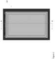
- FIG. 1is a front view of a display assembly indicating section line A-A;
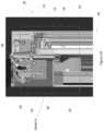
- FIG. 2 Ais a detailed side sectional view of the display assembly of FIG. 1 taken along section line A-A and indicating detail A;
- FIG. 2 Bis a detailed perspective view of detail A of FIG. 2 A ;
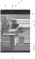
- FIG. 3 Ais a perspective view of a second heat exchange substructure using fasteners for use with the display assembly of FIG. 1 indicating detail B;
- FIG. 3 Bis a detailed perspective view of detail B of FIG. 3 A ;
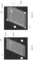
- FIG. 4 Ais a perspective view of an exemplary second heat exchange substructure using structural adhesive for use with the display assembly of FIG. 1 and indicating detail C;
- FIG. 4 Bis a detailed perspective view of detail C of FIG. 4 A ;
- FIG. 5 Ais a perspective view of a first heat exchange substructure using fasteners for use with the display assembly of FIG. 1 also indicating details D and F, as well as section line B-B;
- FIG. 5 Bis a perspective view of a first heat exchange substructure using structural adhesive for use with the display assembly of FIG. 1 also indicating details E and G, as well as section line C-C;
- FIG. 6 Ais a detailed perspective view of detail D of FIG. 5 A ;
- FIG. 6 Bis a detailed perspective view of detail E of FIG. 5 B ;
- FIG. 7 Ais another detailed perspective view of detail F of FIG. 5 A ;
- FIG. 7 Bis another detailed perspective view of detail G of FIG. 5 B ;
- FIG. 8 Ais a cross sectional perspective view taken along section line B-B of FIG. 5 A ;
- FIG. 8 Bis a cross sectional perspective view taken along section line C-C of FIG. 5 B ;
- FIG. 9is a flow chart for an exemplary process for creating the display assembly, or subassemblies thereof, using structural adhesive
- FIG. 10is a perspective view of an exemplary first heat exchange substructure partially completed and undergoing manufacture.
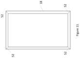
- FIG. 11is a rear view of an exemplary portion of the housing of the assembly of FIG. 1 .
- Embodiments of the inventionare described herein with reference to illustrations of idealized embodiments (and intermediate structures) of the invention. As such, variations from the shapes of the illustrations as a result, for example, of manufacturing techniques and/or tolerances, are to be expected. Thus, embodiments of the invention should not be construed as limited to the particular shapes of regions illustrated herein but are to include deviations in shapes that result, for example, from manufacturing.
- FIG. 1 through FIG. 2 Billustrate an exemplary display assembly 10 .
- the assembly 10may comprise a housing 18 .
- the assembly 10may comprise a cover layer 12 .
- the cover layer 12may comprise a single layer or multiple layers 12 A, 12 B bonded together, such as by way of an optical adhesive.
- the cover layer 12may be positioned forward of an electronic display layer 14 .
- the cover layer 12may be secured to the housing 18 , directly or indirectly.
- the electronic display layer 14may be secured to the housing 18 , directly or indirectly.
- the electronic display layer 14may comprise a layer of liquid crystals (e.g., an LCD), a plasma display, OLED display, LED display, combinations thereof, or the like.
- the cover layer 12may be transparent or translucent such that images displayed at the electronic display layer 14 are visible to an intended viewer through the cover layer 12 .
- the cover layer 12may comprise one or more polarizers, anti-reflective films, surface treatments, combinations thereof, or the like.
- the cover layer 12may be configured to protect and/or enhance optics of the images displayed at the electronic display layer 14 .
- a front gap 13may extend between the cover layer 12 and the electronic display layer 14 .
- the front gap 13comprises a channel which may form part of a closed loop airflow pathway for circulating gas.
- the cover layer 12may be optically bonded to the electronic display layer 14 .
- a backlight 16may be provided rearward of the electronic display layer 14 .
- the backlight 16may comprise multiple light emitting diodes (LEDs) or other light sources configured to illuminate the electronic display layer 14 when powered.
- the backlight 16may comprise multiple light sources mounted to one or more panels 24 .
- the backlight 16may comprise multiple tiles or blocks of light sources, each of which may be connected to a power source and/or a driver, which may be individual to the tile or block or common to multiple tiles or blocks.
- the backlight 16may be configured to provide direct backlighting to the electronic display layer 14 .
- the backlight 16may be configured to provide edge lighting to the electronic display layer 14 , such as directly, or by way of one or more diffusers, reflection elements, combinations thereof, or the like. Where emissive type electronic display layers 14 are utilized, a separate backlight 16 may not be required.
- the assembly 10may comprise one or more thermal management substructures, including, but not necessarily limited to, a first heat exchange substructure 20 .
- the first heat exchange substructure 20may comprise a single or multiple layer heat exchanger, by way of non-limiting example.
- the first heat exchange substructure 20may be provided rearward of the backlight 16 and/or the electronic display layer 14 .
- the first heat exchange substructure 20may extend, directly or indirectly, along some or all of the backlight 16 and/or electronic display layer 14 so as to absorb some or all of the heat generated by the backlight 16 and/or electronic display layer 14 when in use.
- the first heat exchange substructure 20may extend directly along a rear panel of the backlight 16 , though such is not required.
- the panel 24may form a portion of the first heat exchange substructure 20 , though spacing and/or other layers between the panel 24 and the first heat exchange substructure 20 may be provided.
- the first heat exchange substructure 20may comprise a corrugated layer 26 .
- the corrugated layer 26may comprise a single sheet of material bent to form peaks and valleys in exemplary embodiments.
- the corrugated layer 26may comprise multiple sheets, panels, portions, and/or subcomponents which together form the corrugated layer 26 .
- the corrugated layer 26may comprise a zig-zag pattern which extends between two or more panels, thereby forming a number of subchannels or pathways, such as which are part of a larger channel or pathway.
- the first heat exchange substructure 20may comprise a number of tubes (e.g., square, rectangular, round, combinations thereof, or the like).
- the corrugated layer 26may be secured to the panel 24 , though such is not required.
- the corrugated layer 26may be secured to another panel of the first heat exchange substructure 20 separate from the panel 24 and forming part of the backlight 16 .
- the first heat exchange substructure 20may comprise a second panel 28 .
- the corrugated layer 26 and/or channelsmay extend between two panels of the first heat exchange substructure 20 to form passageways. Where the corrugated layer 26 comprises multiple parts, each part may be secured to the panel 24 , second panel 28 , and/or other component(s), by way of non-limiting example.
- the first heat exchange substructure 20may form part of an open loop airflow pathway configured to accept ambient air.
- the first heat exchange substructure 20may be in fluid communication with one or more intakes and exhausts provided in the housing 18 .
- intakes and exhaustsmay comprise one or more apertures.
- the thermal management substructure of the assembly 10may comprise other components, including, but not necessarily limited to, a second heat exchange substructure 22 .
- the second heat exchange substructure 22may comprise a multi-layer heat exchanger, by way of non-limiting example.
- the second heat exchange substructure 22may be provided rearward of the backlight 16 and/or electronic display layer 14 .
- the second heat exchange substructure 22may be provided rearward of the first heat exchange substructure 20 .
- the second heat exchange substructure 22may comprise multiple layers 36 , at least some of which may form part of a same or a different open loop airflow pathway as the first heat exchange substructure 20 , and at least some of which may form part of the same or a different closed loop airflow pathway as the front gap 13 . Notably, the front gap 13 may not be required.
- the closed loop airflow pathwaymay extend within the housing 18 .
- the second heat exchange substructure 22may be in fluid communication with the same or different intakes and exhausts as the first heat exchange substructure 20 .
- the second heat exchange substructure 22may be in fluid communication with the front gap 13 , though such is not required.
- the first and second heat exchange substructures 20 , 22may be mechanically separated from, or connected to, one another.
- the display assembly 10may comprise multiple electronic display layers 14 .
- the display assembly 10may comprise multiple cover layers 12 , backlights 16 , first heat exchange substructure 20 , second heat exchange substructure 22 , combinations thereof, or the like.
- at least the second heat exchange substructure 22may be common to multiple electronic display layers 14 in some embodiments.
- the display assembly 10may comprise a first and second electronic display layer 14 provided in a back-to-back arrangement, such as with front gaps 13 fluidly connected to a common second heat exchange substructure 22 but which each utilize separate first heat exchange substructures 20 , one for each electronic display layer 14 for example, without limitation. Such an arrangement is not required.
- any number and/or arrangement of open loop airflow pathways, sub-pathways, channels, subchannels, or the likemay be provided.
- any number and/or arrangement of closed loop airflow pathways, sub-pathways, channels, subchannels, or the likemay be provided.
- Any number and type of first heat exchange substructures 20 and/or second heat exchange substructures 22may be provided.
- one or more of the first heat exchange substructure 20 and/or second heat exchange substructure 22may be used within the display assembly 10 .
- Any number or type of electronic display layers 14may be utilized which may share some or all parts of a thermal management substructure, or have entirely separate thermal management substructures.
- the electronic display layer 14self-illuminates, for example, without limitation, where the electronic display layer 14 comprises plasma, OLED, LEDs, combinations thereof, or the like, a separate backlight 16 may not be required.
- the first heat exchange substructure 20if utilized, may be provided along some or all of the electronic display layer 14 .
- the assembly 10may comprise one or more fans. Some of the fans may be provided within the open loop airflow pathways for moving ambient air when activated. Other of the fans may be provided within the closed loop airflow pathways for moving circulating gas when activated. In other exemplary embodiments, fans may be common to both the open and closed loop airflow pathways.
- the ambient air within the open loop airflow pathwaymay be entirely or substantially prevented from mixing with the circulating gas of the closed loop airflow pathway.
- the display assemblymay be configured to comply with various ingress protection standards, such as, but not limited to, IP 65, IP 66, IP 67, IP 68, combinations thereof, or the like.
- Ambient airmay comprise air ingested from the surrounding environment and may be filtered.
- the circulating gasmay comprise air kept fully or partially separate from the ambient air.
- the circulating gasmay be ambient air trapped when the assembly 10 is formed or otherwise periodically accessed (e.g., for servicing).
- the circulating gasmay comprise filtered or purified air.
- the first heat exchange substructures 20 and/or second heat exchange substructures 22may be configured to facilitate such separation.
- the first heat exchange substructures 20 and/or second heat exchange substructures 22may be of any type, including, but not limited to, cross flow, counter flow, co-current, counter current, hybrid, direct, indirect, parallel flow, shell and tube, tube in tube, double tube, plate type heat exchangers, combinations thereof, or the like.
- one or both of the first heat exchange substructures 20 and/or second heat exchange substructures 22may be configured to mix air between the open and closed loops and may comprise a mixing chamber, by way of non-limiting example.
- FIG. 3 A and FIG. 3 Billustrate an embodiment of the second heat exchange substructure 22 A using fasteners 34 .
- the second heat exchange substructure 22 Amay comprise a number of layers 36 . Some of the layers 36 may form part of one or more of the open loop airflow pathways for ambient air, and some others may form part of one or more of the closed loop airflow pathways for circulating gas. For example, without limitations, the layers 36 may be configured to alternately accept ambient air and circulating gas on a layer-by-layer basis.
- the second heat exchange substructure 22 Amay comprise one or more panels 30 , such as, but not limited to, a front and rear panel. One or more members 32 may extend between the panels 30 and/or along some or all of the layers 36 .
- Such members 32may be spaced apart along some or all of the second heat exchange substructure 22 A. Such members 32 may, alternatively or additionally, be provided between layers 36 to space the layers 36 apart.
- the second heat exchange substructure 22 Amay comprise a number of fasteners 34 provided on the panel(s) 30 , the layer(s) 36 , and/or the members 32 .
- the fasteners 34may penetrate through one or more of the panels 30 , the layers 36 , and/or the members 32 .
- the fasteners 34may comprise screws, rivets, bolts, nails, combinations thereof, or the like.
- FIG. 4 A and FIG. 4 Billustrates another embodiment of the second heat exchange substructure 22 B using structural adhesive.
- the second heat exchange substructure 22 Bmay have the same, or similar, components arranged in the same or similar manner as the second heat exchange substructure 22 A, though such is not required. Fewer or no fasteners 34 may be utilized compared to the second heat exchange substructure 22 B. Instead of some or all of the fasteners 34 , a structural adhesive may be utilized with the second heat exchange substructure 22 B. In exemplary embodiments, the structural adhesive may be provided between each layer 36 , at the members 32 , at the panels 30 A, 30 B, combinations thereof, or the like.
- the structural adhesivemay, alternatively or additionally, be provided on outer portions of the second heat exchange substructure 22 B to connect the second heat exchange substructure 22 B to other components of the display assembly 10 , such as, but not limited to, the panel 24 , the second panel 24 B, the housing 18 , the first heat exchange substructure 20 A, 20 B, the backlight 16 , a structural member, other component, combinations thereof, or the like.
- the open loop airflow pathway for the second heat exchange substructure 22 Bmay be at least partially separated from the open loop airflow pathway for the first heat exchange substructure 20 B.
- ambient airmay be ingested through separate intakes and exhausted through separate exhausts.
- ambient airmay be ingested through a common intake and separated so that a first portion travels through a first open loop airflow pathway to the first heat exchange substructure 20 B and a second portion travels through a second open loop airflow pathway to the second heat exchange substructure 22 B before being exhausted through separate, or common, exhausts.
- Second heat exchange substructures 22 Bmay be utilized in a display assembly 10 and/or a single second heat exchange substructure 22 B may be broken up into portions or sections.
- FIG. 5 A , FIG. 6 A , FIG. 7 A , and FIG. 8 Aillustrate an embodiment of the first heat exchange substructure 20 A using fasteners 34 .
- the fasteners 34may be provided along peaks and/or valleys of the corrugated layer 26 .
- Multiple corrugated layers 26may be provided, such as adopt one another, adjacent to one another, combinations thereof, or the like. Alternatively, or additionally, the corrugated layers 26 may be provided in multiple portions.
- the fasteners 34may extend through front or rear panels of the first heat exchange substructure 20 A and/or to the panel 24 , the second panel 28 , the backlight 16 , the housing 18 , structural member, other component, combinations thereof, or the like.
- FIG. 5 B , FIG. 6 B , FIG. 7 B , and FIG. 8 Billustrate an embodiment of the first heat exchange substructure 20 B using structural adhesive.
- the first heat exchange substructure 20 Bmay have the same, or similar, components arranged in the same or similar manner to the first heat exchange substructure 20 A, though such is not required.
- fewer or no fasteners 34may be utilized.
- the structural adhesivemay be utilized.
- the structural adhesivemay be provided along the peaks and/or valleys of the corrugated layer 26 .
- the structural adhesivemay connect the corrugated layer 26 to front and/or rear panels of the first heat exchange substructure 20 B, such as, but not limited to, the panel 24 , the second panel 28 , combinations thereof, or the like.
- the structural adhesivemay be provided on outer surfaces of the first heat exchange substructure 20 B to connect the first heat exchange substructure 20 B to other components of the display assembly 10 such as, but not limited to, the second heat exchange substructure 22 A, 22 B, the backlight 16 , the housing 18 , structural member, other component, combinations thereof, or the like.
- FIG. 9explains how the assembly 10 , or components thereof, such as, but not limited to, the first heat exchange substructure 20 B and/or the second heat exchange substructure 22 B may be created or otherwise partially or fully manufactured using the structural adhesive.
- FIG. 10provides an example of a portion of the assembly 10 , and specifically of an exemplary first heat exchange substructure 20 B, partially assembled. The process shown and/or described herein may be utilized for any number of components of the assembly 10 , including, but not limited to, the second heat exchange substructure 22 B.
- the structural adhesivemay be prepared. Preparation of the structural adhesive may include mixing one or more materials.
- the structural adhesivemay comprise a pressure sensitive adhesive.
- the pressure sensitive adhesive (“PSA”)may be a natural rubber PSA, synthetic rubber PSA, acrylic PSA, silicon PSA, combinations thereof, or the like. Other types or kinds of adhesives may alternatively, or additionally, be utilized.
- the adhesive or other portion of the structural adhesivemay comprise multiple parts which require mixing before application.
- the adhesive or other portion of the structural adhesivemay be mixed with, or otherwise include, a spacing material.
- the spacing materialmay comprise an inert material.
- the spacing materialmay comprise glass beads of a particular size, such as, but not limited to, 10/1000ths of an inch, though any size or multiple sizes may be used, such as, but not limited to, between 1/1000ths of an inch and 100/1000ths of an inch.
- the utilizing of a spacing material as part of, or with, the structural adhesivemay provide the necessary gap between components for the adhesive to remain and activate application. For example, without the spacing material the adhesive may otherwise be displaced upon sufficient compression of the components.
- the spacing materialmay, alternatively, or additionally, be utilized to provide increased dimensional accuracy of the resulting subassemblies and/or display assembly 10 by providing more exact and consistent spacing between adhered components.
- the tolerance and consistency of resulting spacing using the structural adhesive with spacing materialmay be improved relative to the use of fasteners 34 .
- the spacing materialmay be applied at 2.5% by weight into part or all of the structural adhesive and mixed until substantially homogenous, though any amount may be utilized such as, but not limited to, between 0.5% and 10% by weight.
- the structural adhesivemay be mixed by a computer-controlled system 48 .
- the system 48may comprise one or more reservoirs comprising components of the structural adhesive.
- the system 48may comprise one or more pumps or other components for drawing or otherwise forcing the components of the structural adhesive together, such as, but not limited to, into a mixing chamber, through one or more tubes, combinations thereof, or the like.
- the system 48may comprise, or be in electronic communication with, one or more temperature sensors, pressure sensors, combinations thereof, or the like, and may adjust an amount, flow rate, percentage, combinations thereof, or the like of the components of the structural adhesive utilized based on readings from the sensors.
- a componentmay be placed on a table 38 .
- the componentmay be a part of the first or second heat exchange substructure 20 , 22 , the housing 18 , or another component of the assembly 10 by way of non-limiting example.
- the table 38may comprise a substantially planar upper surface to improve flatness of the resulting subassembly and/or display assembly 10 .
- Such placementmay be achieved by one or more robots 50 .
- the componentsmay be retrieved from one or more material carts and/or autonomous guided vehicles (AGVs), including, but not limited to, those provided by AGILOX Systems GmbH (www.agilox.net/en/).
- the one or more robots 50may comprise material handling robots, such as, but not limited to, those available from FANUC America Corp.
- the one or more robots 50may be placed on a track and may have a reach of approximately 10 ft.
- the componentmay be secured to the table 38 , such as by a vacuum, clamps, static weight, the one or more robots, combinations thereof, or the like.
- the table 38 and/or at least one of the one or more robotsmay be those available from AXYZ Automation Inc. of Burlington, Ontario, Canada (www.axyz.com/us/) though any type or kind of table 38 may be utilized.
- the component secured to the table 38may comprise a front or rear panel 24 , 28 of the first heat exchange substructure 20 B, a front or rear panel 30 A, 30 B of the second heat exchange substructure 22 B, the housing 18 or component thereof, combinations thereof, or the like. However, any component of the assembly 10 may be so secured.
- a structural adhesivemay be applied to the secured component.
- the structural adhesivein exemplary embodiments, may be applied by the system 48 and/or one or more robots 40 .
- the table 38may comprise one or more gantry-based robots 40 configured to automatically prepare and/or apply the structural adhesive to desired locations on the component.
- the robots 40may comprise fluid dispensing robots in exemplary embodiments.
- Additional componentsmay be applied on top of the secured component to further complete a subassembly.
- the structural adhesivemay be applied to the non-secured component. Additional applications of structural adhesive may be applied, and additional components secured as needed to complete the subassembly.
- an additional panel 24 , 28 of the first heat exchange substructure 20 Bmay be provided.
- additional layers 36 and/or panels 30 A, 30 Bmay be provided.
- one or more components of the assembly 10such as, but not limited to, the first heat exchange substructure 20 and/or the second heat exchange substructure 22 , may be manufactured.
- any number, kind, and/or type of components and/or substructures for the assembly 10may be manufactured in this fashion.
- such completed components and/or substructuresmay be installed at the assembly 10 in this fashion.
- weightmay be added.
- the weightmay be static weight and may comprise a number of plywood and/or medium density fiberboard sheets stacked atop a polymer sheet.
- the weightsmay be positioned manually, by the one or more robots, a forklift, combinations thereof, or the like.
- 1.25 lbs./sq. in. of structural adhesive contact areamay be applied to a given subassembly or the assembly 10 . This may translate to, for example, without limitation, approximately 400 lbs. of weight applied to display assemblies 10 comprising a 55-inch electronic display layer 14 , and approximately 600 lbs. for display assemblies 10 comprising a 75-inch electronic display layer 14 .
- any ratiomay be utilized such as, but not limited to, between 0.5 and 5 lbs./sq. in.
- the structural adhesivemay be cured. Curing may be accomplished by the passage of time (e.g., 30-120 mins), the addition of the weights, application of light (e.g., visible spectrum, UV, etc.), application of an accelerate or other material, exposure to ambient or forced airflow, combination thereof, or the like. In exemplary embodiments, curing may be accomplished and/or accelerated by exposing the structural adhesive to particular temperatures, light sources, materials, combinations thereof, or the like. However, such applications and/or curing may be performed at room temperature or ambient conditions.
- the structural adhesivemay be applied at locations where troughs or ridges of the corrugated layer 26 attach to the panel 24 , the second panel 28 , different portions of the corrugated layer 26 , combinations thereof, or the like. If tubes are utilized, the structural adhesive may be applied at locations where the tubes connect to the panel 24 , the second panel 28 , other tubes, combinations thereof, or the like.
- the structural adhesivemay be applied between layers 36 , to different portions of the layers 36 , at the front or rear panels 30 A, 30 B, at the members 32 , combinations thereof, or the like to secure such components to one another.
- the structural adhesivemay be applied to any component(s) of, and at any location within, the display assembly 10 in any pattern or amount.
- the structural adhesivemay comprise one or more pressure sensitive adhesives.
- the structural adhesivemay comprise one or more methyl methacrylate adhesives.
- the structural adhesivemay comprise those available from PLEXUS Corp., under the PLEXUS® brand of Neenah, WI (www.plexus.com/en-us/) including, but not limited to, MA8110 and/or MA8120 for example, without limitation. Any type or kind of structural adhesive may be utilized.
- the completed subassemblymay be released from the table 38 , moved to another location, and/or joined with other subassemblies (such as by way of the structural adhesive, though such is not required) to form the display assembly 10 .
- the completed subassemblymay be joined to other components of the assembly 10 using the same or different structural adhesive, though such is not required.
- Such movementmay be made by one or more robots, manually, combinations thereof, or the like.
- the use of structural adhesive in place of fasteners 34may provide a number of advantages in the resulting subassembly (e.g., second heat exchange substructure 22 B, first heat exchange substructure 20 B, or other component) and/or display assembly 10 .
- torsional rigiditymay be improved, strength may be increased, noise may be decreased (e.g., from 70 dB to 60 dB), tolerances may be improved, vibrations may be decreased, additional layers may be added to the second heat exchange substructure 22 B and/or first heat exchange substructure 20 B to increase cooling, sealing may be improved resulting in a decreased need for cooling, less material and/or labor may be required for assembly (e.g., 1.25 man hours to 0.6 man hours), holes may not need cut for fasteners 34 resulting in less work, fewer potential leak points, increased strength and rigidity, combinations thereof, and the like.
- dimensional accuracymay be improved by decreasing bond line thicknesses (e.g., from 30/1000ths of an inch to 10/1000ths of an inch) thereby providing more room, increasing thermal conductivity between components, combinations thereof, and the like.
- consistency of spacingmay be increased, particularly by use of the spacing material in the adhesive, thereby improvising dimensional accuracy and consistency.
- the overall size of the second heat exchange substructure 22 B and/or first heat exchange substructure 20 B, or components thereof (e.g., corrugated layer 26 and/or layers 36 ),may be increased due to the tightened tolerances and/or increased dimensional accuracy.
- the resulting subassemblies and/or assembly 10may be flatter and may resist bowing, resulting in greater sealing between components such as the first heat exchange substructure 20 B, which may be provided within an access assembly 44 comprising the electronic display assembly 14 attached to the housing 18 by way of one or more hinges 46 . This may result in a decreased amount of force required between the access assembly 44 and the housing 18 to maintain a seal with a gasket 42 which may extend between the housing 18 and the access assembly.
- the structural adhesivemay be used in place of other joints and/or to attach other components of the display assembly 10 .
- the structural adhesivemay be used in fasteners or welding.
- the structural adhesivemay be used at corner joints 52 of the housing 18 , other housings and/or structural members for various subassemblies, other components of the display assembly 10 , combinations thereof, or the like.
- An example of where the structural adhesive may be used at corner joints 52 of the housing 18is provided at FIG. 11 as an example, without limitation. This may reduce or eliminate the need for welding and subsequent grinding and finishing.
- corner joints for a frame of the access panel subassembly 44may be joined by structural adhesive.
- welding such componentsmay result in shrinkage to an hourglass shape making it difficult to accommodate the cover layer 12 .
- the use of structural adhesivemay reduce or eliminate this problem.
- four membersmay be formed into a substantially rectangular shape, and the structural adhesive may be applied at mitered edges of the joint, such as in place of welding.
- the membersmay be secured by clamps, by robots, combinations thereof, or the like, while the structural adhesive cures. This may provide a squarer resulting framework to accommodate a squarer cover layer 12 .
- Any number, size, and/or shape membersmay be used to provide any type, kind, and/or shape of framework.
- Adhered componentsmay be subsequently finished, such as by cleaning, surface treatment, further assembly, painting, powder coating, combinations thereof, or the like, though such is not required.
- the various components shown and/or described hereinmay comprise one or more metals, polymers, combinations thereof, or the like.
- the various components of the first heat exchange substructure 20 , the second heat exchange substructure 22 , and/or components thereofe.g., the layers 36 , the members 32 , and/or the corrugated layer 26 ) and/or attached thereto (e.g., the housing 18 , the panel 24 , and/or the second panel 28 ) comprise metal.
- the various componentsmay be cut, pressed, and/or bended sheets of metal, such as steel, aluminum, titanium, combinations thereof, or the like.
- any embodiment of the present inventionmay include any of the features of the other embodiments of the present invention.
- the exemplary embodiments herein disclosedare not intended to be exhaustive or to unnecessarily limit the scope of the invention.
- the exemplary embodimentswere chosen and described in order to explain the principles of the present invention so that others skilled in the art may practice the invention. Having shown and described exemplary embodiments of the present invention, those skilled in the art will realize that many variations and modifications may be made to the described invention. Many of those variations and modifications will provide the same result and fall within the spirit of the claimed invention. It is the intention, therefore, to limit the invention only as indicated by the scope of the claims.
- Each electronic devicemay comprise one or more processors, electronic storage devices, executable software instructions, and the like configured to perform the operations described herein.
- the electronic devicesmay be general purpose computers or a specialized computing device.
- the electronic devicesmay comprise personal computers, smartphones, tablets, databases, servers, or the like.
- the electronic connections and transmissions described hereinmay be accomplished by wired or wireless means.
- the computerized hardware, software, components, systems, steps, methods, and/or processes described hereinmay serve to improve the speed of the computerized hardware, software, systems, steps, methods, and/or processes described herein.
Landscapes
- Physics & Mathematics (AREA)
- Nonlinear Science (AREA)
- Optics & Photonics (AREA)
- Crystallography & Structural Chemistry (AREA)
- Chemical & Material Sciences (AREA)
- General Physics & Mathematics (AREA)
- Mathematical Physics (AREA)
- Engineering & Computer Science (AREA)
- Microelectronics & Electronic Packaging (AREA)
- Thermal Sciences (AREA)
- Devices For Indicating Variable Information By Combining Individual Elements (AREA)
- Casings For Electric Apparatus (AREA)
- Adhesives Or Adhesive Processes (AREA)
- Cooling Or The Like Of Electrical Apparatus (AREA)
- Adhesive Tapes (AREA)
Abstract
Description
Claims (12)
Priority Applications (3)
| Application Number | Priority Date | Filing Date | Title |
|---|---|---|---|
| US17/669,439US12197060B2 (en) | 2021-02-12 | 2022-02-11 | Display assembly using structural adhesive |
| US18/243,136US12055809B2 (en) | 2021-02-12 | 2023-09-07 | Display assembly using structural adhesive |
| US18/970,066US12436422B2 (en) | 2021-02-12 | 2024-12-05 | Display assembly using structural adhesive |
Applications Claiming Priority (2)
| Application Number | Priority Date | Filing Date | Title |
|---|---|---|---|
| US202163148703P | 2021-02-12 | 2021-02-12 | |
| US17/669,439US12197060B2 (en) | 2021-02-12 | 2022-02-11 | Display assembly using structural adhesive |
Related Child Applications (2)
| Application Number | Title | Priority Date | Filing Date |
|---|---|---|---|
| US18/243,136ContinuationUS12055809B2 (en) | 2021-02-12 | 2023-09-07 | Display assembly using structural adhesive |
| US18/970,066DivisionUS12436422B2 (en) | 2021-02-12 | 2024-12-05 | Display assembly using structural adhesive |
Publications (2)
| Publication Number | Publication Date |
|---|---|
| US20220260872A1 US20220260872A1 (en) | 2022-08-18 |
| US12197060B2true US12197060B2 (en) | 2025-01-14 |
Family
ID=82801339
Family Applications (3)
| Application Number | Title | Priority Date | Filing Date |
|---|---|---|---|
| US17/669,439Active2042-07-25US12197060B2 (en) | 2021-02-12 | 2022-02-11 | Display assembly using structural adhesive |
| US18/243,136ActiveUS12055809B2 (en) | 2021-02-12 | 2023-09-07 | Display assembly using structural adhesive |
| US18/970,066ActiveUS12436422B2 (en) | 2021-02-12 | 2024-12-05 | Display assembly using structural adhesive |
Family Applications After (2)
| Application Number | Title | Priority Date | Filing Date |
|---|---|---|---|
| US18/243,136ActiveUS12055809B2 (en) | 2021-02-12 | 2023-09-07 | Display assembly using structural adhesive |
| US18/970,066ActiveUS12436422B2 (en) | 2021-02-12 | 2024-12-05 | Display assembly using structural adhesive |
Country Status (6)
| Country | Link |
|---|---|
| US (3) | US12197060B2 (en) |
| EP (1) | EP4291826A4 (en) |
| KR (1) | KR20230144610A (en) |
| AU (2) | AU2022219982B2 (en) |
| CA (1) | CA3210876A1 (en) |
| WO (1) | WO2022174006A1 (en) |
Families Citing this family (9)
| Publication number | Priority date | Publication date | Assignee | Title |
|---|---|---|---|---|
| US9573346B2 (en) | 2008-05-21 | 2017-02-21 | Manufacturing Resources International, Inc. | Photoinitiated optical adhesive and method for using same |
| US11645029B2 (en) | 2018-07-12 | 2023-05-09 | Manufacturing Resources International, Inc. | Systems and methods for remotely monitoring electronic displays |
| WO2022174006A1 (en) | 2021-02-12 | 2022-08-18 | Manufacturing Resourcesinternational, Inc | Display assembly using structural adhesive |
| US11921010B2 (en)* | 2021-07-28 | 2024-03-05 | Manufacturing Resources International, Inc. | Display assemblies with differential pressure sensors |
| US11965804B2 (en)* | 2021-07-28 | 2024-04-23 | Manufacturing Resources International, Inc. | Display assemblies with differential pressure sensors |
| US11972672B1 (en) | 2022-10-26 | 2024-04-30 | Manufacturing Resources International, Inc. | Display assemblies providing open and unlatched alerts, systems and methods for the same |
| US12027132B1 (en) | 2023-06-27 | 2024-07-02 | Manufacturing Resources International, Inc. | Display units with automated power governing |
| US12350730B1 (en) | 2023-12-27 | 2025-07-08 | Manufacturing Resources International, Inc. | Bending mandril comprising ultra high molecular weight material, related bending machines, systems, and methods |
| WO2025212305A1 (en) | 2024-04-04 | 2025-10-09 | Manufacturing Resources International, Inc. | Display assembly using air characteristic data to verify display assembly operating conditions, systems and methods for the same |
Citations (258)
| Publication number | Priority date | Publication date | Assignee | Title |
|---|---|---|---|---|
| US2986379A (en) | 1957-06-04 | 1961-05-30 | Kramig Anna Louise | Heat exchanger |
| US3784586A (en) | 1969-10-30 | 1974-01-08 | Pechiney Saint Gobain | Copolymerizable composition of oligo-esters having maleic acid end groups and vinyl monomers |
| US3823794A (en) | 1971-11-25 | 1974-07-16 | Saint Gobain | Acoustical panels |
| US3858965A (en) | 1972-07-10 | 1975-01-07 | Minolta Camera Kk | Five layer anti-reflection coating |
| US4007552A (en) | 1973-09-04 | 1977-02-15 | Abc Extrusion Company | Extruded aluminum sign frame system |
| US4093355A (en) | 1977-02-04 | 1978-06-06 | General Motors Corporation | Symmetrical internal heater for liquid crystal display |
| US4297401A (en) | 1978-12-26 | 1981-10-27 | Minnesota Mining & Manufacturing Company | Liquid crystal display and photopolymerizable sealant therefor |
| US4299639A (en) | 1976-08-07 | 1981-11-10 | Franz Xaver Bayer Isolierglasfabrik Kg | Method for the production of laminates with spaced-apart glass panes |
| US4593978A (en) | 1983-03-18 | 1986-06-10 | Thomson-Csf | Smectic liquid crystal color display screen |
| US4604444A (en) | 1983-10-19 | 1986-08-05 | Rhone-Poulenc Specialites Chimiques | Curable organopolysiloxane compositions comprising microencapsulated hardening accelerators |
| US4634225A (en) | 1984-12-24 | 1987-01-06 | General Electric Co. | Transflective liquid crystal display with integral heating unit and temperature sensor |
| US4640584A (en) | 1984-03-24 | 1987-02-03 | Nippon Shokubai Kagaku Kogyo Co., Ltd. | Spacers for liquid crystal display device |
| JPS62197335A (en) | 1986-02-25 | 1987-09-01 | Natl House Ind Co Ltd | Production of sandwich glass |
| US4691995A (en) | 1985-07-15 | 1987-09-08 | Semiconductor Energy Laboratory Co., Ltd. | Liquid crystal filling device |
| US4712875A (en) | 1985-05-15 | 1987-12-15 | Canon Kabushiki Kaisha | Dimensions of spacer particles for a ferroelectric liquid crystal display |
| US4715686A (en) | 1984-11-16 | 1987-12-29 | Seiko Epson Corporation | Light-passive display device and method of manufacturing same |
| US4724023A (en) | 1985-04-09 | 1988-02-09 | E M Partners Ag | Method of making laminated glass |
| US4766176A (en) | 1987-07-20 | 1988-08-23 | Dow Corning Corporation | Storage stable heat curable organosiloxane compositions containing microencapsulated platinum-containing catalysts |
| US4896218A (en) | 1987-09-04 | 1990-01-23 | Rockwell International Corporation | Circularly polarized multi-bandpass interference contrast enhancement filter |
| US4950344A (en) | 1988-12-05 | 1990-08-21 | Lauren Manufacturing Company | Method of manufacturing multiple-pane sealed glazing units |
| US5029982A (en) | 1989-09-11 | 1991-07-09 | Tandy Corporation | LCD contrast adjustment system |
| US5059484A (en) | 1989-03-13 | 1991-10-22 | Dow Corning Corporation | Optically clear composites comprising two layer of organic polymers and an organosiloxane adhesive |
| US5066699A (en) | 1990-08-31 | 1991-11-19 | Dow Corning Corporation | Storage stable heat curable organosiloxane compositions containing a microencapsulated catalyst and method for preparing said catalyst |
| US5088806A (en) | 1990-01-16 | 1992-02-18 | Honeywell, Inc. | Apparatus and method for temperature compensation of liquid crystal matrix displays |
| US5148591A (en) | 1981-05-11 | 1992-09-22 | Sensor Adaptive Machines, Inc. | Vision target based assembly |
| US5247374A (en) | 1990-04-05 | 1993-09-21 | Stanley Electric Co., Ltd. | Liquid crystal display device with common heater between two cells |
| US5330262A (en) | 1992-12-21 | 1994-07-19 | Transfer Flow International, Inc. | Coved backsplash for a countertop |
| US5365354A (en) | 1990-10-02 | 1994-11-15 | Physical Optics Corporation | Grin type diffuser based on volume holographic material |
| US5379139A (en) | 1986-08-20 | 1995-01-03 | Semiconductor Energy Laboratory Co., Ltd. | Liquid crystal device and method for manufacturing same with spacers formed by photolithography |
| US5402141A (en) | 1992-03-11 | 1995-03-28 | Honeywell Inc. | Multigap liquid crystal color display with reduced image retention and flicker |
| US5406399A (en) | 1991-12-17 | 1995-04-11 | Sony Corporation | Liquid crystal display apparatus having a frame around periphery and bottom and extending above both polarizers |
| JPH08194437A (en) | 1995-01-13 | 1996-07-30 | Matsushita Electric Works Ltd | Display device |
| US5548038A (en) | 1994-03-31 | 1996-08-20 | Dow Corning Toray Silicone Co., Ltd. | Organosiloxane compositions yielding optically clear, non-yellowing organosiloxane gels |
| US5547483A (en) | 1992-12-29 | 1996-08-20 | Pixel International | Spacers for flat display screens |
| US5559614A (en) | 1995-05-01 | 1996-09-24 | Motorola, Inc. | Liquid crystal display with integral heater and method of fabricating same |
| JPH08271883A (en) | 1995-03-31 | 1996-10-18 | Sekisui Chem Co Ltd | Glass cell laminated body for liquid crystal display |
| US5601915A (en) | 1994-03-18 | 1997-02-11 | Nippon Carbide Kogyo Kabushiki Kaisha | Retroreflective sheeting |
| US5606438A (en) | 1994-06-11 | 1997-02-25 | Motorola, Inc. | Rugged liquid crystal display and method of manufacture |
| US5610742A (en) | 1991-08-01 | 1997-03-11 | Seiko Epson Corporation | Liquid crystal display element, methods of producing and storing the same, and electronic equipment on which the same is mounted |
| US5656824A (en) | 1995-06-02 | 1997-08-12 | Ois Optical Imaging Systems, Inc. | TFT with reduced channel length and method of making same |
| US5661210A (en) | 1996-09-25 | 1997-08-26 | Dow Corning Corporation | Optically clear liquid silicone rubber |
| US5748269A (en) | 1996-11-21 | 1998-05-05 | Westinghouse Air Brake Company | Environmentally-sealed, convectively-cooled active matrix liquid crystal display (LCD) |
| US5767489A (en) | 1994-12-14 | 1998-06-16 | Hewlett-Packard Company | Enhanced resolution liquid crystal microthermography method and apparatus |
| US5818010A (en) | 1995-10-31 | 1998-10-06 | Smiths Industries Plc | Display assemblies |
| US5838405A (en) | 1995-03-31 | 1998-11-17 | Sharp Kabushiki Kaisha | Tiled display device |
| US5852484A (en) | 1994-09-26 | 1998-12-22 | Matsushita Electric Industrial Co., Ltd. | Liquid crystal display panel and method and device for manufacturing the same |
| US5869919A (en) | 1994-06-09 | 1999-02-09 | Canon Kabushiki Kaisha | Air cooling for flat panel displays |
| US5899027A (en) | 1997-07-28 | 1999-05-04 | Haden, Inc. | Contaminant shield |
| US5911899A (en) | 1995-06-15 | 1999-06-15 | Mitsui Chemicals, Inc. | Corrosion-proof transparent heater panels and preparation process thereof |
| JPH11160727A (en) | 1997-12-01 | 1999-06-18 | Advanced Display Inc | Liquid crystal display device |
| US5937611A (en) | 1995-09-28 | 1999-08-17 | Howes; Stephen E. | Method of making an impact resistant window |
| US5991153A (en) | 1997-10-31 | 1999-11-23 | Lacerta Enterprises, Inc. | Heat transfer system and method for electronic displays |
| US6020945A (en) | 1996-11-11 | 2000-02-01 | Dowa Mining Co., Ltd. | Display device with a transparent optical filter |
| US6074741A (en) | 1997-03-27 | 2000-06-13 | Tomoegawa Paper Co., Ltd. | Antiglare material and polarizing film using the same |
| US6089751A (en) | 1996-12-30 | 2000-07-18 | Honeywell Inc. | Transparent temperature sensor for an active matrix liquid crystal display |
| US6099672A (en) | 1996-03-23 | 2000-08-08 | Semiconductor Energy Laboratory Co., Ltd. | Method of manufacturing liquid crystal device |
| US6157432A (en) | 1999-01-29 | 2000-12-05 | Hewlett-Packard Company | Heated ferroelectric liquid crystal spatial light modulator with improved contrast, improved grayscale resolution, and decreased pixel sticking when operated in a non-DC balanced mode |
| US6191839B1 (en) | 1999-05-03 | 2001-02-20 | Rockwell Collin, Inc. | Patterned thermal sensor |
| US6198515B1 (en) | 1998-03-16 | 2001-03-06 | Joseph W. Cole | Apparatus and method for controlled sealing between bezel and CRT |
| US6211934B1 (en) | 1997-12-24 | 2001-04-03 | Honeywell Inc. | Method of and apparatuses for reducing infrared loading on display devices |
| JP3153212B2 (en) | 1999-01-06 | 2001-04-03 | ファイザー製薬株式会社 | Isochromane compound and method for producing the same |
| US6219127B1 (en) | 1998-01-12 | 2001-04-17 | Semiconductor Energy Laboratory Co., Ltd. | Display device |
| US20010001459A1 (en) | 1998-08-20 | 2001-05-24 | Physical Optics Corporation | Method of manufacturing a diffuser master using a blasting agent |
| US20010019454A1 (en) | 1998-10-23 | 2001-09-06 | Biljana Tadic-Galeb | Projection lens and system |
| US20010043293A1 (en) | 1999-12-27 | 2001-11-22 | Hiromoto Inoue | Liquid crystal display device |
| US6359390B1 (en) | 1997-04-07 | 2002-03-19 | Mitsubishi Denki Kabushiki Kaisha | Display device |
| US20020033919A1 (en) | 1999-01-22 | 2002-03-21 | Sanelle Joseph J. | Super bright low reflectance liquid crystal display |
| US20020042162A1 (en) | 2000-10-05 | 2002-04-11 | Masashi Tone | Method of forming electrode section on inner surface of transparent electromagnetic wave shielding plate, and transparent electromagnetic wave shielding plate formed thereby |
| US6392727B1 (en) | 1998-12-31 | 2002-05-21 | Honeywell International Inc. | Reduced reflectance polarized display |
| JP2002158475A (en) | 2000-11-20 | 2002-05-31 | Fujitsu General Ltd | Sealed housing for flat panel display |
| US6398371B1 (en) | 2000-09-22 | 2002-06-04 | Fuji Photo Film Co., Ltd. | Antiglare film, method for producing the same, polarizer and liquid crystal display |
| US6417900B1 (en) | 1997-03-21 | 2002-07-09 | Lg. Philips Lcd Co., Ltd. | Liquid crystal display unit with conductive light-shielding member having substantially the same potential as common electrode |
| US6421103B2 (en) | 1999-12-28 | 2002-07-16 | Fuji Photo Film Co., Ltd. | Liquid-crystal display apparatus including a backlight section using collimating plate |
| US20020101553A1 (en) | 2001-01-31 | 2002-08-01 | Fujitsu Limited | Liquid-crystal display device having a shield shielding an electromagnetic wave radiated from one of a driver and an electrode lead-out line |
| US6437673B1 (en) | 1997-02-18 | 2002-08-20 | Canon Kabushiki Kaisha | Transformer assembling method, transformer, transformer-mounted substrate, power supply unit having transformer-mounted substrate, and recording apparatus including power supply unit |
| US6446467B1 (en) | 1997-07-29 | 2002-09-10 | Physical Optics Corporation | Monolithic glass light shaping diffuser and method for its production |
| US20020126248A1 (en) | 2001-03-07 | 2002-09-12 | Takamasa Yoshida | Display device |
| US6451870B1 (en) | 1998-06-24 | 2002-09-17 | Henkel Loctite Corporation | Dual curing silicone compositions |
| US6465092B1 (en) | 1996-08-14 | 2002-10-15 | Asahi Kogaku Kogyo Kabushiki Kaisha | Adhesive transparent resin and a composite including the same |
| US20020149714A1 (en) | 2001-04-16 | 2002-10-17 | Robert Anderson | Ruggedized flat panel display assembly |
| US6472032B1 (en) | 1998-03-17 | 2002-10-29 | Nippon Sheet Glass Co., Ltd. | Double-glazing unit |
| US20020187575A1 (en) | 2001-04-27 | 2002-12-12 | Semiconductor Energy Laboratory Co., Ltd. | Display device and manufacturing method thereof |
| US20020186333A1 (en) | 2001-05-07 | 2002-12-12 | Jin-Ho Ha | Liquid crystal display device and method for assembling the same |
| US6504713B1 (en) | 1998-01-22 | 2003-01-07 | Iv Phoenix Group, Inc. | Ultra-rugged, high-performance computer system |
| US20030007109A1 (en) | 2001-05-18 | 2003-01-09 | Sang-Hoon Park | Liquid crystal display |
| US6512562B1 (en) | 1999-04-15 | 2003-01-28 | Konica Corporation | Protective film for polarizing plate |
| US20030026085A1 (en) | 2001-07-31 | 2003-02-06 | Nec Corporation | Backlight unit uniformly illuminating object regardless of lapse of time and liquid crystal display panel device using the same |
| US6535266B1 (en) | 1999-12-16 | 2003-03-18 | Rockwell Collins, Inc. | Closed loop LCD heater system |
| US6555235B1 (en) | 2000-07-06 | 2003-04-29 | 3M Innovative Properties Co. | Touch screen system |
| US20030090810A1 (en) | 2001-11-08 | 2003-05-15 | Michael Detro | Method and apparatus for packaging optical elements |
| US6611302B1 (en) | 1999-07-14 | 2003-08-26 | Nec Lcd Technologies, Ltd. | Flat panel display device |
| US6628355B1 (en) | 1996-12-17 | 2003-09-30 | Matsushita Electric Industrial Co., Ltd. | Liquid crystal display panel including a light shielding film to control incident light |
| US6650393B1 (en) | 1998-11-11 | 2003-11-18 | Minolta Co., Ltd. | Liquid crystal light modulating device and a method for manufacturing same |
| US6683639B2 (en) | 2001-06-08 | 2004-01-27 | Oce-Technologies, B.V. | Printhead for an image-forming apparatus and an image-forming apparatus containing the same |
| US20040018375A1 (en) | 2002-07-05 | 2004-01-29 | Koji Banno | Transparent electromagnetic wave-shielding laminate for display, process for producing same and display unit |
| US6692986B1 (en) | 1999-09-09 | 2004-02-17 | Osram Opto Semiconductors Gmbh | Method for encapsulating components |
| US20040032638A1 (en) | 1999-07-09 | 2004-02-19 | Tonar William L. | Electrochromic devices with thin bezel-covered edge |
| US20040036834A1 (en) | 2002-08-22 | 2004-02-26 | Noriaki Ohnishi | Liquid crystal display device, image shifting device, and image display apparatus |
| US20040062029A1 (en) | 2002-09-17 | 2004-04-01 | Nec Lcd Technologies, Ltd. | Backlight for a double-sided liquid crystal display unit |
| US6727468B1 (en) | 2001-08-06 | 2004-04-27 | Rockwell Collins | Flexible heating system having high transmissivity |
| WO2004036270A1 (en) | 2002-10-14 | 2004-04-29 | 3M Innovative Properties Company | Antireflection films for use with displays |
| US6731367B1 (en) | 1998-12-04 | 2004-05-04 | Seiko Epson Corporation | Electro-optical panel, electro-optical panel module, and projection display device |
| US6731357B1 (en) | 1999-01-27 | 2004-05-04 | Konica Corporation | Cellulose ester film, production method of the same, film employed in liquid crystal display member, and polarizing plate |
| US20040105159A1 (en) | 2002-09-20 | 2004-06-03 | Saccomanno Robert J. | High efficiency viewing screen |
| US6747720B2 (en) | 2000-03-27 | 2004-06-08 | Nitto Denko Corporation | Polarizing plate with optical compensation film and liquid crystal display |
| US20040113044A1 (en) | 2002-12-13 | 2004-06-17 | Advanced Display Inc. | Light source unit and display device |
| AU2003285975A1 (en) | 2002-12-02 | 2004-06-23 | Rpo Pty Limited | Process for producing polysiloxanes and use of the same |
| US6762471B2 (en) | 2000-11-13 | 2004-07-13 | Mems Solutions Inc. | Thin film resonator and method for manufacturing the same |
| JP2004205599A (en) | 2002-12-24 | 2004-07-22 | Victor Co Of Japan Ltd | Reflective liquid crystal display element |
| US20040145805A1 (en)* | 2003-01-16 | 2004-07-29 | Jean Qiu | Unitary device with internal microscopic counting grid used for analysis of microscopic particles contained in liquid |
| US20040155997A1 (en) | 2003-02-11 | 2004-08-12 | Kent State University | Stressed liquid crystals as an ultra-fast light modulating material consisting of unidirectionally oriented liquid crystal micro-domains separated by polymer chains |
| US6779252B2 (en) | 1999-02-17 | 2004-08-24 | Applied Kinetics, Inc. | Apparatus for assembling components |
| US20040165139A1 (en) | 2003-02-21 | 2004-08-26 | Anderson Grady K. | Liquid crystal cell platform |
| KR20040097466A (en) | 2003-05-12 | 2004-11-18 | 엘지.필립스 엘시디 주식회사 | Liquid crystal display moudule |
| US6825899B2 (en) | 2000-02-29 | 2004-11-30 | Alps Electric Co., Ltd. | Liquid crystal display device in which generation of moire fringes is prevented |
| GB2402205A (en) | 2003-05-20 | 2004-12-01 | Densitron Technologies Plc | A display system cabinet and display system including heat removal means |
| US20040239823A1 (en) | 2001-08-13 | 2004-12-02 | Silsby Paul Alistair | Display |
| US6830348B2 (en) | 2000-07-19 | 2004-12-14 | Fuji Photo Film Co., Ltd. | Antiglare and antireflection film, polarizer, and image display device |
| US6839104B2 (en) | 2000-11-22 | 2005-01-04 | Fujitsu Display Technologies Corporation | Common electrode substrate and liquid crystal display device having the same |
| US20050012722A1 (en) | 2003-07-18 | 2005-01-20 | Hwa-Su Chon | Touch screen |
| JP2005029579A (en) | 2000-10-06 | 2005-02-03 | Jsr Corp | Resin composition and three-dimensional shape |
| JP2005055641A (en) | 2003-08-04 | 2005-03-03 | Yokogawa Electric Corp | Liquid crystal display |
| US20050062373A1 (en) | 2003-09-20 | 2005-03-24 | Myoung-Kon Kim | Filter holder and display apparatus including the same |
| US6873387B2 (en) | 2000-02-28 | 2005-03-29 | Fuji Photo Film Co., Ltd. | Antireflection film, sheet polarizer and liquid crystal display device |
| US20050073632A1 (en) | 2003-10-07 | 2005-04-07 | American Panel Corporation | Flat panel display having integral heater, EMI shield, and thermal sensors |
| US20050073640A1 (en) | 2003-10-07 | 2005-04-07 | American Panel Corporation | Flat panel display having integral heater, EMI shield, and thermal sensors |
| JP2005121940A (en) | 2003-10-17 | 2005-05-12 | Toyo Ink Mfg Co Ltd | Polymerizable composition, negative resist using the same, and image pattern forming method using the same |
| US20050105178A1 (en) | 2003-11-13 | 2005-05-19 | Samsung Electronics Co., Ltd. | Projection television and manufacturing method thereof |
| JP2005134849A (en) | 2003-10-31 | 2005-05-26 | Nagoya Electric Works Co Ltd | Information display device |
| US20050117110A1 (en)* | 2003-12-02 | 2005-06-02 | Byun Young S. | Loader and bonding apparatus for fabricating liquid crystal display device and loading method thereof |
| US20050115670A1 (en) | 2001-10-29 | 2005-06-02 | Armand Bettinelli | Method and device for etching a thin conductive layer which is disposed on an insulating plate such as to form an electrode network thereon |
| US6909486B2 (en) | 2003-02-18 | 2005-06-21 | Ran-Hong Raymond Wang | Liquid crystal display viewable under all lighting conditions |
| US20050134526A1 (en) | 2003-12-23 | 2005-06-23 | Patrick Willem | Configurable tiled emissive display |
| JP2005225793A (en) | 2004-02-12 | 2005-08-25 | Kyowa Hakko Chemical Co Ltd | Phosphine oxide compound |
| WO2005079129A1 (en) | 2004-02-16 | 2005-08-25 | Inssimainos Oy | Procedure and apparatus for controlling the temperature of a display surface |
| US6943768B2 (en) | 2003-02-21 | 2005-09-13 | Xtellus Inc. | Thermal control system for liquid crystal cell |
| US20050212990A1 (en) | 2004-03-22 | 2005-09-29 | Robinder Ronald C | Frame for rugged mounting for bonded LCD |
| US6955833B1 (en) | 1998-12-01 | 2005-10-18 | Pilkington Plc | Coating glass |
| US20050286131A1 (en) | 2004-06-25 | 2005-12-29 | Ragini Saxena | Optical compensation of cover glass-air gap-display stack for high ambient lighting |
| KR20060016469A (en) | 2004-08-18 | 2006-02-22 | 삼성전자주식회사 | Backlight unit and liquid crystal display including the same |
| EP1640337A2 (en) | 2004-09-27 | 2006-03-29 | Idc, Llc | Apparatus and methods for arranging micromechanical devices into an interconnected array |
| US20060082271A1 (en) | 2004-10-15 | 2006-04-20 | Lee Seung M | Light emitting device package and back light unit for liquid crystral display using the same |
| US20060082700A1 (en) | 2004-10-15 | 2006-04-20 | Gehlsen Mark D | Composite diffuser plates and direct-lit liquid crystal displays using same |
| US20060092348A1 (en) | 2004-10-30 | 2006-05-04 | Lg, Philips Lcd Co., Ltd. | Backlight unit and liquid crystal display with the same |
| US20060103299A1 (en) | 2004-11-15 | 2006-05-18 | The Hong Kong University Of Science And Technology | Polycrystalline silicon as an electrode for a light emitting diode & method of making the same |
| US7052152B2 (en) | 2003-10-03 | 2006-05-30 | Philips Lumileds Lighting Company, Llc | LCD backlight using two-dimensional array LEDs |
| US7059757B2 (en) | 2002-07-17 | 2006-06-13 | Sharp Kabushiki Kaisha | Liquid crystal display device |
| US20060132699A1 (en) | 2004-12-20 | 2006-06-22 | Cho Joo-Woan | Cooling apparatus and liquid crystal display device having the same |
| EP1678534A1 (en) | 2003-10-27 | 2006-07-12 | RPO Pty Limited | Planar waveguide with patterned cladding and method for producing same |
| US20060159867A1 (en) | 2005-01-19 | 2006-07-20 | O'donnell Stephen D | High-strength optical bonding method using optical silicone as a bonding medium and pressure sensitive adhesive as an intermediate layer |
| US7083285B2 (en) | 2003-06-13 | 2006-08-01 | Coretronic Corporation | Cooling structure for projection apparatus |
| AU2006214795A1 (en) | 2005-02-15 | 2006-08-24 | Rpo Pty Limited | Photolithographic patterning of polymeric materials |
| US20060209266A1 (en) | 2005-03-17 | 2006-09-21 | Nec Viewtechnology, Ltd. | Projection display apparatus using liquid cooling and air cooling |
| US20060262258A1 (en) | 2005-05-23 | 2006-11-23 | Wang Ran-Hong R | Controlling polarization for liquid crystal displays |
| US20060274237A1 (en) | 2005-06-03 | 2006-12-07 | 3M Innovative Properties Company | Brightness Enhancing Film and Display Device Having the Same |
| US20060279946A1 (en) | 2005-06-08 | 2006-12-14 | Mun-Soo Park | Backlight assembly, display device provided with the same, and method for assembling backlight assembly |
| US20060289201A1 (en) | 2005-06-22 | 2006-12-28 | Gi-Cherl Kim | Backlight assembly, display device having the same, and method thereof |
| US7161642B2 (en) | 2002-12-26 | 2007-01-09 | Lg. Philips Lcd Co., Ltd. | Liquid crystal display module and assembling method thereof |
| KR100666961B1 (en) | 2005-08-18 | 2007-01-10 | 주식회사 파이컴 | Back light device |
| US7194158B2 (en) | 2003-08-08 | 2007-03-20 | Schott Ag | Method for producing light-scattering structures on flat optical waveguides |
| US20070065091A1 (en) | 2005-09-22 | 2007-03-22 | Sanyo Epson Imaging Devices Corporation | Electro-optical device, electronic apparatus, protective member, and method of manufacturing protective member |
| US20070103854A1 (en) | 2005-11-04 | 2007-05-10 | Chuan-Pei Yu | Liquid crystal display |
| US7232250B2 (en) | 2005-05-16 | 2007-06-19 | Chih-Lun Chuang | Prism sheet |
| US20070139574A1 (en) | 2005-12-19 | 2007-06-21 | Byung-Soo Ko | Plateless LCD Unit |
| KR20070070675A (en) | 2005-12-29 | 2007-07-04 | 노틸러스효성 주식회사 | LCD cooling module and financial automation equipment using the same |
| US20070151664A1 (en) | 2005-12-29 | 2007-07-05 | Lg.Philips Lcd Co., Ltd. | Cooling apparatus and method for manufacturing liquid crystal display device using the same |
| US20070200095A1 (en) | 2006-02-02 | 2007-08-30 | Nichia Corporation | Phosphor and light emitting device using the same |
| US20070206158A1 (en) | 2006-03-06 | 2007-09-06 | Seiko Epson Corporation | Optical device and projector |
| US20070230218A1 (en) | 2006-03-29 | 2007-10-04 | 3M Innovative Properties Company | Optical film assemblies and methods of making same |
| US7295179B2 (en) | 2003-01-31 | 2007-11-13 | American Panel Corporation | Flat panel display having multiple display areas on one glass substrate |
| US20070268201A1 (en) | 2006-05-22 | 2007-11-22 | Sampsell Jeffrey B | Back-to-back displays |
| US20070267174A1 (en) | 2006-05-18 | 2007-11-22 | Lg Electronics Inc. | Heat sink of plasma display apparatus |
| US20070279556A1 (en) | 2005-05-23 | 2007-12-06 | Wang Ran-Hong R | Controlling polarization for liquid crystal displays |
| TW200809287A (en) | 2006-05-02 | 2008-02-16 | Rpo Pty Ltd | Methods for fabricating polymer optical waveguides on large area substrates |
| US20080049164A1 (en) | 2006-08-22 | 2008-02-28 | Samsung Electronics Co., Ltd., | Backlight assembly, manufacturing method thereof, and liquid crystal display device |
| US20080083906A1 (en) | 2006-10-06 | 2008-04-10 | Nemoto & Company, Ltd. | Orange-emitting phosphor |
| AU2003242399B2 (en) | 2002-08-29 | 2008-04-24 | Rpo Pty Ltd | Hindered Siloxanes |
| US20080111949A1 (en) | 2006-06-30 | 2008-05-15 | Sony Corporation | Backlight device, liquid crystal display device, and electronic apparatus |
| US20080111958A1 (en) | 2006-11-09 | 2008-05-15 | Sony Ericsson Mobile Communications Ab | Display with variable reflectivity |
| EP1923406A1 (en) | 2005-08-11 | 2008-05-21 | Kyowa Hakko Chemical Co., Ltd. | Resin composition |
| KR20080046335A (en) | 2006-11-22 | 2008-05-27 | 삼성전자주식회사 | Storage module for display device, backlight assembly and display device having same |
| US20080146709A1 (en) | 2006-12-15 | 2008-06-19 | Shin -Etsu Chemical Co., Ltd. | Addition curable silicone adhesive composition and cured product thereof |
| US20080151082A1 (en) | 2006-12-22 | 2008-06-26 | Chen-Hung Chan | Dead pixel real-time detection method for image |
| US20080176345A1 (en) | 2007-01-19 | 2008-07-24 | Texas Instruments Inc. | Ebeam inspection for detecting gate dielectric punch through and/or incomplete silicidation or metallization events for transistors having metal gate electrodes |
| US20080230177A1 (en) | 2007-03-19 | 2008-09-25 | White Electronic Designs Corp. | Enhanced liquid crystal display system and methods |
| KR20080086245A (en) | 2007-03-22 | 2008-09-25 | 삼성전자주식회사 | Backlight assembly and liquid crystal display including the same |
| TW200838901A (en) | 2006-10-17 | 2008-10-01 | Rpo Pty Ltd | Process for producing polysiloxanes and use of the same |
| US20080261057A1 (en) | 2007-04-20 | 2008-10-23 | White Electronic Designs Corp. | Bezelless display system |
| US20080284942A1 (en) | 2004-08-18 | 2008-11-20 | Kazutoshi Mahama | Backlight Device and Transmission Type Liquid Crystal Display Apparatus |
| JP2008292743A (en) | 2007-05-24 | 2008-12-04 | Necディスプレイソリューションズ株式会社 | Cooling device, and electronic equipment and projection type display device equipped with cooling device |
| US20090015761A1 (en) | 2007-05-04 | 2009-01-15 | Itronix Corporation | Combination transparent touch panel liquid crystal display stack and methods of manufacturing same |
| US20090015747A1 (en) | 2007-07-10 | 2009-01-15 | Hitachi Displays, Ltd. | Display device |
| US20090021915A1 (en)* | 2007-07-17 | 2009-01-22 | Inventec Multimedia & Telecom (Tianjin) Co., Ltd. | Multi-layer heat-dissipating device |
| US7481566B2 (en) | 2006-03-27 | 2009-01-27 | Lg. Display Co., Ltd | Light emitting diode backlight unit and liquid crystal display having the same |
| US7481553B2 (en) | 2006-06-26 | 2009-01-27 | Lg Display Co., Ltd. | Backlight assembly and liquid crystal display module using the same |
| US20090104989A1 (en) | 2007-10-23 | 2009-04-23 | Igt | Separable backlighting system |
| US20090153780A1 (en) | 2005-09-30 | 2009-06-18 | Sharp Kabushiki Kaisha | Liquid crystal display and television receiver |
| US20090251650A1 (en) | 2005-08-22 | 2009-10-08 | Fujifilm Corporation | Liquid crystal display device |
| US20100039696A1 (en) | 2008-08-12 | 2010-02-18 | Qualcomm Mems Technologies, Inc. | Method and apparatus to reduce or eliminate stiction and image retention in interferometric modulator devices |
| US20100043966A1 (en) | 2008-05-21 | 2010-02-25 | Manufacturing Resources International, Inc. | Photoinitiated optical adhesive and method for using same |
| US20100098839A1 (en) | 2007-04-10 | 2010-04-22 | Tomoyuki Toyoda | Method for producing image display apparatus |
| US7798694B2 (en) | 2005-10-24 | 2010-09-21 | Lg Electronics Inc. | Thermal layer, backlight unit and display device including the same |
| US20100253660A1 (en) | 2009-04-02 | 2010-10-07 | Tpo Displays Corp. | Display device and electronic apparatus equipped with the same |
| US7812919B2 (en) | 2006-08-07 | 2010-10-12 | Kent State University | Cholesteric liquid crystal light modulators |
| US20100307800A1 (en) | 2006-02-10 | 2010-12-09 | Opulent Electronics International Pte Ltd | Anodised Aluminum, Dielectric, and Method |
| US20110019363A1 (en) | 2009-07-23 | 2011-01-27 | Scott Vahlsing | Field serviceable display device |
| US7922381B2 (en) | 2003-06-26 | 2011-04-12 | Samsung Electronics Co., Ltd. | Two-way backlight assembly and two-way liquid crystal display apparatus having the same |
| US20110090630A1 (en) | 2009-10-16 | 2011-04-21 | Apple Inc. | Portable computer display housing |
| WO2011049564A1 (en) | 2009-10-21 | 2011-04-28 | Manufacturing Resources International, Inc. | Photoinitiated optical adhesive and method for using same |
| TW201114716A (en) | 2009-10-30 | 2011-05-01 | Mri Inc | Photoinitiated optical adhesive and method for using same |
| US20110194053A1 (en) | 2004-05-21 | 2011-08-11 | Tannas Lawrence E | Apparatus and methods for cutting electronic displays during resizing |
| US8004648B2 (en) | 2007-11-16 | 2011-08-23 | Manufacturing Resources International, Inc. | Air curtain for display |
| US20110205472A1 (en) | 2010-02-19 | 2011-08-25 | Hitachi Displays, Ltd. | Display device and liquid crystal display device and method of manufacturing the same |
| US8009262B2 (en) | 2005-02-14 | 2011-08-30 | American Panel Corporation | Flat panel display wtih external integral heater |
| US20110221995A1 (en) | 2008-11-10 | 2011-09-15 | Tovis Co., Ltd. | Liquid crystal display with a plurality of liquid crystal display modules |
| US8120595B2 (en) | 2006-05-01 | 2012-02-21 | Rpo Pty Limited | Waveguide materials for optical touch screens |
| US20120050958A1 (en) | 2010-08-27 | 2012-03-01 | Emery Sanford | Electronic devices with component mounting structures |
| US20120069273A1 (en) | 2009-06-03 | 2012-03-22 | Sharp Kabushiki Kaisha | Display device |
| US20120111479A1 (en) | 2010-11-05 | 2012-05-10 | Kuo-Hua Sung | Curved touch panel |
| WO2012073929A1 (en) | 2010-12-02 | 2012-06-07 | シャープ株式会社 | Liquid crystal display device and multi-display system |
| US20120154712A1 (en) | 2010-12-16 | 2012-06-21 | Shang-Wen Yu | Liquid crystal display device and backlight module thereof |
| US8208115B2 (en) | 2007-11-16 | 2012-06-26 | Manufacturing Resources International, Inc. | Fluid cooled display |
| US8242974B2 (en) | 1995-10-05 | 2012-08-14 | Semiconductor Energy Laboratory Co., Ltd. | Three dimensional display unit and display method |
| US8269916B2 (en) | 2008-07-24 | 2012-09-18 | Sony Corporation | Light emitting device assembly, surface light source device, liquid crystal display device assembly, and light output member |
| US8274626B2 (en) | 2007-03-15 | 2012-09-25 | Cheil Industries, Inc. | Diffuser prism sheet with light diffusing element on valley region, LCD back light unit including the same, and LCD device including the same |
| US20120242926A1 (en) | 2010-11-22 | 2012-09-27 | Wistron Corporation | Liquid crystal display device and electronic equipment having the same |
| US8294168B2 (en) | 2010-06-04 | 2012-10-23 | Samsung Electronics Co., Ltd. | Light source module using quantum dots, backlight unit employing the light source module, display apparatus, and illumination apparatus |
| US20120275023A1 (en) | 2009-10-24 | 2012-11-01 | Weber Michael F | Immersed reflective polarizer with angular confinement in selected planes of incidence |
| US20120287368A1 (en) | 2011-05-10 | 2012-11-15 | Shenzhen China Star Optoelectronics Technology Co., Ltd. | LCD Device and Back Cover Thereof |
| US20120295051A1 (en) | 2008-05-21 | 2012-11-22 | Manufacturing Resources International, Inc. | Glass assembly |
| US20130027633A1 (en) | 2011-07-29 | 2013-01-31 | Lg Innotek Co., Ltd | Lighting Device and Liquid Crystal Display Using the Same |
| US20130051200A1 (en) | 2011-08-29 | 2013-02-28 | Seiko Epson Corporation | Cover glass and timepiece |
| CN202815379U (en) | 2012-09-13 | 2013-03-20 | 宁波永望电子科技有限公司 | Liquid crystal display |
| US20130094160A1 (en) | 2011-10-14 | 2013-04-18 | Japan Display East Inc. | Display device |
| US20130163277A1 (en) | 2011-12-26 | 2013-06-27 | Samsung Display Co., Ltd. | Display module and apparatus having the same |
| US20130206063A1 (en) | 2011-08-12 | 2013-08-15 | Pieter Terblanche Janse Van Rensburg | Adhesive application apparatus and methods |
| US8529993B2 (en) | 2006-05-01 | 2013-09-10 | Zetta Research andDevelopment LLC—RPO Series | Low volatility polymers for two-stage deposition processes |
| US20130329363A1 (en) | 2012-04-06 | 2013-12-12 | Manufacturing Resources International, Inc. | Apparatus and Method for Assembling Large Electronic Displays |
| US8674390B2 (en) | 2011-05-31 | 2014-03-18 | Nanoco Technologies Ltd. | Semiconductor nanoparticle-containing materials and light emitting devices incorporating the same |
| US8674963B2 (en) | 2006-09-22 | 2014-03-18 | Zetta Research and Development LLC—RPO Series | Waveguide configurations for optical touch systems |
| US8711321B2 (en) | 2007-11-16 | 2014-04-29 | Manufacturing Resources International, Inc. | System for thermally controlling displays |
| US20140118221A1 (en) | 2012-10-25 | 2014-05-01 | Samsung Display Co., Ltd. | Two side display device and manufacturing method thereof |
| US8827472B2 (en) | 2010-09-24 | 2014-09-09 | Sony Corporation | Display apparatus, optical member, and method of manufacturing an optical member |
| US20140268657A1 (en) | 2013-03-14 | 2014-09-18 | Manufacturing Resources International, Inc. | Rigid LCD Assembly |
| US20140285732A1 (en) | 2013-03-22 | 2014-09-25 | Semiconductor Energy Laboratory Co., Ltd. | Liquid crystal display device |
| WO2014149502A1 (en) | 2013-03-15 | 2014-09-25 | Manufacturing Resources International, Inc. | Glass assembly on monitor array |
| US20140321103A1 (en) | 2008-03-03 | 2014-10-30 | Manufacturing Resources International, Inc. | Expanded Heat Sink for Electronic Displays |
| US8879042B2 (en) | 2007-11-16 | 2014-11-04 | Manufacturing Resources International, Inc. | Isolated cooling system having an insulator gap and front polarizer |
| US20150177480A1 (en) | 2013-12-20 | 2015-06-25 | Lockheed Martin Corporation | Condensation inhibiting layer, method of forming the layer, and condensation inhibiting device |
| US20160037657A1 (en) | 2014-07-31 | 2016-02-04 | Semiconductor Energy Laboratory Co., Ltd. | Display device |
| US20170242290A1 (en) | 2016-02-23 | 2017-08-24 | Microsoft Technology Licensing, Llc | Dissipation Layer in a Display Device |
| US9756739B2 (en) | 2012-01-25 | 2017-09-05 | Apple Inc. | Glass device housing |
| US20180086954A1 (en)* | 2016-09-29 | 2018-03-29 | Nitto Denko Corporation | Filler-containing pressure-sensitive adhesive tape and method of producing filler-containing pressure-sensitive adhesive tape |
| US20180366685A1 (en) | 2017-06-19 | 2018-12-20 | Samsung Display Co., Ltd. | Panel bottom sheet and display device including the same |
| US20200285099A1 (en) | 2018-07-04 | 2020-09-10 | Dynascan Technology Corp. | Electronic display assembly |
| US20210046746A1 (en) | 2019-08-15 | 2021-02-18 | Wuhan China Star Optoelectronics Semiconductor Display Technology Co., Ltd. | Flexible display module and flexible display device |
| US20220260872A1 (en) | 2021-02-12 | 2022-08-18 | Manufacturing Resources International, Inc. | Display assembly using structural adhesive |
| US20230002558A1 (en) | 2019-11-08 | 2023-01-05 | The University Of North Carolina At Chapel Hill | Reactive polyamideimide oligomers, methods, and articles |
Family Cites Families (14)
| Publication number | Priority date | Publication date | Assignee | Title |
|---|---|---|---|---|
| US2553961A (en) | 1947-11-14 | 1951-05-22 | John F Dreyer | Laminated polarizer |
| US2907102A (en) | 1955-05-16 | 1959-10-06 | Horace T Potts Company | Cold tube bending |
| US5074092A (en) | 1989-07-31 | 1991-12-24 | Weyerhaeuser Company | Laminated wood product |
| US5823031A (en) | 1996-11-20 | 1998-10-20 | Tools For Bending, Inc. | Method and apparatus for bulge forming and bending tubes |
| US6804118B2 (en)* | 2002-03-15 | 2004-10-12 | Delphi Technologies, Inc. | Thermal dissipation assembly for electronic components |
| JP4031827B2 (en) | 2002-10-10 | 2008-01-09 | 三桜工業株式会社 | Double pipe bending method |
| DE102007050893B4 (en) | 2007-10-24 | 2011-06-01 | Continental Automotive Gmbh | Method for positioning and mounting a LED assembly and positioning body therefor |
| WO2010055822A1 (en) | 2008-11-13 | 2010-05-20 | ポリマテック株式会社 | Method of manufacturing decorated molded element, and decorated molded element |
| WO2012021573A2 (en)* | 2010-08-12 | 2012-02-16 | Manufacturing Resources International, Inc. | Expanded heat sink for electronic displays and method of producing the same |
| CN106062114A (en) | 2014-03-05 | 2016-10-26 | 3M创新有限公司 | Skin friendly (meth)acrylic pressure sensitive adhesive |
| US9925577B2 (en) | 2014-05-16 | 2018-03-27 | Ford Global Technologies, Llc | Rotary-draw bending mandrel with galling-resistive inserts |
| CN207992647U (en)* | 2018-03-29 | 2018-10-19 | 京东方科技集团股份有限公司 | Backlight module and display device |
| US11478838B2 (en) | 2020-11-25 | 2022-10-25 | Rogue Fabrication, LLC | Tube bending systems |
| US11668695B1 (en) | 2022-01-28 | 2023-06-06 | Boise Cascade Company | Method for determining the density of a sheet of material using a magnetic force feedback actuator positioner |
- 2022
- 2022-02-11WOPCT/US2022/016055patent/WO2022174006A1/ennot_activeCeased
- 2022-02-11EPEP22753386.6Apatent/EP4291826A4/enactivePending
- 2022-02-11USUS17/669,439patent/US12197060B2/enactiveActive
- 2022-02-11AUAU2022219982Apatent/AU2022219982B2/enactiveActive
- 2022-02-11CACA3210876Apatent/CA3210876A1/enactivePending
- 2022-02-11KRKR1020237030946Apatent/KR20230144610A/ennot_activeCeased
- 2023
- 2023-09-07USUS18/243,136patent/US12055809B2/enactiveActive
- 2024
- 2024-12-05USUS18/970,066patent/US12436422B2/enactiveActive
- 2024-12-24AUAU2024287207Apatent/AU2024287207A1/enactivePending
Patent Citations (293)
| Publication number | Priority date | Publication date | Assignee | Title |
|---|---|---|---|---|
| US2986379A (en) | 1957-06-04 | 1961-05-30 | Kramig Anna Louise | Heat exchanger |
| US3784586A (en) | 1969-10-30 | 1974-01-08 | Pechiney Saint Gobain | Copolymerizable composition of oligo-esters having maleic acid end groups and vinyl monomers |
| US3823794A (en) | 1971-11-25 | 1974-07-16 | Saint Gobain | Acoustical panels |
| US3858965A (en) | 1972-07-10 | 1975-01-07 | Minolta Camera Kk | Five layer anti-reflection coating |
| US4007552A (en) | 1973-09-04 | 1977-02-15 | Abc Extrusion Company | Extruded aluminum sign frame system |
| US4299639A (en) | 1976-08-07 | 1981-11-10 | Franz Xaver Bayer Isolierglasfabrik Kg | Method for the production of laminates with spaced-apart glass panes |
| US4093355A (en) | 1977-02-04 | 1978-06-06 | General Motors Corporation | Symmetrical internal heater for liquid crystal display |
| US4297401A (en) | 1978-12-26 | 1981-10-27 | Minnesota Mining & Manufacturing Company | Liquid crystal display and photopolymerizable sealant therefor |
| US5148591A (en) | 1981-05-11 | 1992-09-22 | Sensor Adaptive Machines, Inc. | Vision target based assembly |
| US4593978A (en) | 1983-03-18 | 1986-06-10 | Thomson-Csf | Smectic liquid crystal color display screen |
| US4604444A (en) | 1983-10-19 | 1986-08-05 | Rhone-Poulenc Specialites Chimiques | Curable organopolysiloxane compositions comprising microencapsulated hardening accelerators |
| US4640584A (en) | 1984-03-24 | 1987-02-03 | Nippon Shokubai Kagaku Kogyo Co., Ltd. | Spacers for liquid crystal display device |
| US4715686A (en) | 1984-11-16 | 1987-12-29 | Seiko Epson Corporation | Light-passive display device and method of manufacturing same |
| US4634225A (en) | 1984-12-24 | 1987-01-06 | General Electric Co. | Transflective liquid crystal display with integral heating unit and temperature sensor |
| US4724023A (en) | 1985-04-09 | 1988-02-09 | E M Partners Ag | Method of making laminated glass |
| US4712875A (en) | 1985-05-15 | 1987-12-15 | Canon Kabushiki Kaisha | Dimensions of spacer particles for a ferroelectric liquid crystal display |
| US4691995A (en) | 1985-07-15 | 1987-09-08 | Semiconductor Energy Laboratory Co., Ltd. | Liquid crystal filling device |
| JPS62197335A (en) | 1986-02-25 | 1987-09-01 | Natl House Ind Co Ltd | Production of sandwich glass |
| US5379139A (en) | 1986-08-20 | 1995-01-03 | Semiconductor Energy Laboratory Co., Ltd. | Liquid crystal device and method for manufacturing same with spacers formed by photolithography |
| US4766176A (en) | 1987-07-20 | 1988-08-23 | Dow Corning Corporation | Storage stable heat curable organosiloxane compositions containing microencapsulated platinum-containing catalysts |
| US4896218A (en) | 1987-09-04 | 1990-01-23 | Rockwell International Corporation | Circularly polarized multi-bandpass interference contrast enhancement filter |
| US4950344A (en) | 1988-12-05 | 1990-08-21 | Lauren Manufacturing Company | Method of manufacturing multiple-pane sealed glazing units |
| US5059484A (en) | 1989-03-13 | 1991-10-22 | Dow Corning Corporation | Optically clear composites comprising two layer of organic polymers and an organosiloxane adhesive |
| US5029982A (en) | 1989-09-11 | 1991-07-09 | Tandy Corporation | LCD contrast adjustment system |
| US5088806A (en) | 1990-01-16 | 1992-02-18 | Honeywell, Inc. | Apparatus and method for temperature compensation of liquid crystal matrix displays |
| US5247374A (en) | 1990-04-05 | 1993-09-21 | Stanley Electric Co., Ltd. | Liquid crystal display device with common heater between two cells |
| US5066699A (en) | 1990-08-31 | 1991-11-19 | Dow Corning Corporation | Storage stable heat curable organosiloxane compositions containing a microencapsulated catalyst and method for preparing said catalyst |
| US5365354A (en) | 1990-10-02 | 1994-11-15 | Physical Optics Corporation | Grin type diffuser based on volume holographic material |
| US5610742A (en) | 1991-08-01 | 1997-03-11 | Seiko Epson Corporation | Liquid crystal display element, methods of producing and storing the same, and electronic equipment on which the same is mounted |
| US5406399A (en) | 1991-12-17 | 1995-04-11 | Sony Corporation | Liquid crystal display apparatus having a frame around periphery and bottom and extending above both polarizers |
| US5402141A (en) | 1992-03-11 | 1995-03-28 | Honeywell Inc. | Multigap liquid crystal color display with reduced image retention and flicker |
| US5330262A (en) | 1992-12-21 | 1994-07-19 | Transfer Flow International, Inc. | Coved backsplash for a countertop |
| US5547483A (en) | 1992-12-29 | 1996-08-20 | Pixel International | Spacers for flat display screens |
| US5601915A (en) | 1994-03-18 | 1997-02-11 | Nippon Carbide Kogyo Kabushiki Kaisha | Retroreflective sheeting |
| US5548038A (en) | 1994-03-31 | 1996-08-20 | Dow Corning Toray Silicone Co., Ltd. | Organosiloxane compositions yielding optically clear, non-yellowing organosiloxane gels |
| US5869919A (en) | 1994-06-09 | 1999-02-09 | Canon Kabushiki Kaisha | Air cooling for flat panel displays |
| US5606438A (en) | 1994-06-11 | 1997-02-25 | Motorola, Inc. | Rugged liquid crystal display and method of manufacture |
| US5852484A (en) | 1994-09-26 | 1998-12-22 | Matsushita Electric Industrial Co., Ltd. | Liquid crystal display panel and method and device for manufacturing the same |
| US5767489A (en) | 1994-12-14 | 1998-06-16 | Hewlett-Packard Company | Enhanced resolution liquid crystal microthermography method and apparatus |
| JPH08194437A (en) | 1995-01-13 | 1996-07-30 | Matsushita Electric Works Ltd | Display device |
| US5838405A (en) | 1995-03-31 | 1998-11-17 | Sharp Kabushiki Kaisha | Tiled display device |
| JPH08271883A (en) | 1995-03-31 | 1996-10-18 | Sekisui Chem Co Ltd | Glass cell laminated body for liquid crystal display |
| US5559614A (en) | 1995-05-01 | 1996-09-24 | Motorola, Inc. | Liquid crystal display with integral heater and method of fabricating same |
| US5656824A (en) | 1995-06-02 | 1997-08-12 | Ois Optical Imaging Systems, Inc. | TFT with reduced channel length and method of making same |
| US5911899A (en) | 1995-06-15 | 1999-06-15 | Mitsui Chemicals, Inc. | Corrosion-proof transparent heater panels and preparation process thereof |
| US5937611A (en) | 1995-09-28 | 1999-08-17 | Howes; Stephen E. | Method of making an impact resistant window |
| US8242974B2 (en) | 1995-10-05 | 2012-08-14 | Semiconductor Energy Laboratory Co., Ltd. | Three dimensional display unit and display method |
| US5818010A (en) | 1995-10-31 | 1998-10-06 | Smiths Industries Plc | Display assemblies |
| US6099672A (en) | 1996-03-23 | 2000-08-08 | Semiconductor Energy Laboratory Co., Ltd. | Method of manufacturing liquid crystal device |
| US6465092B1 (en) | 1996-08-14 | 2002-10-15 | Asahi Kogaku Kogyo Kabushiki Kaisha | Adhesive transparent resin and a composite including the same |
| US5661210A (en) | 1996-09-25 | 1997-08-26 | Dow Corning Corporation | Optically clear liquid silicone rubber |
| US6020945A (en) | 1996-11-11 | 2000-02-01 | Dowa Mining Co., Ltd. | Display device with a transparent optical filter |
| US5748269A (en) | 1996-11-21 | 1998-05-05 | Westinghouse Air Brake Company | Environmentally-sealed, convectively-cooled active matrix liquid crystal display (LCD) |
| US6628355B1 (en) | 1996-12-17 | 2003-09-30 | Matsushita Electric Industrial Co., Ltd. | Liquid crystal display panel including a light shielding film to control incident light |
| US6089751A (en) | 1996-12-30 | 2000-07-18 | Honeywell Inc. | Transparent temperature sensor for an active matrix liquid crystal display |
| US6437673B1 (en) | 1997-02-18 | 2002-08-20 | Canon Kabushiki Kaisha | Transformer assembling method, transformer, transformer-mounted substrate, power supply unit having transformer-mounted substrate, and recording apparatus including power supply unit |
| US6417900B1 (en) | 1997-03-21 | 2002-07-09 | Lg. Philips Lcd Co., Ltd. | Liquid crystal display unit with conductive light-shielding member having substantially the same potential as common electrode |
| US6074741A (en) | 1997-03-27 | 2000-06-13 | Tomoegawa Paper Co., Ltd. | Antiglare material and polarizing film using the same |
| US6359390B1 (en) | 1997-04-07 | 2002-03-19 | Mitsubishi Denki Kabushiki Kaisha | Display device |
| US5899027A (en) | 1997-07-28 | 1999-05-04 | Haden, Inc. | Contaminant shield |
| US6446467B1 (en) | 1997-07-29 | 2002-09-10 | Physical Optics Corporation | Monolithic glass light shaping diffuser and method for its production |
| US5991153A (en) | 1997-10-31 | 1999-11-23 | Lacerta Enterprises, Inc. | Heat transfer system and method for electronic displays |
| JPH11160727A (en) | 1997-12-01 | 1999-06-18 | Advanced Display Inc | Liquid crystal display device |
| US6211934B1 (en) | 1997-12-24 | 2001-04-03 | Honeywell Inc. | Method of and apparatuses for reducing infrared loading on display devices |
| US7283185B2 (en) | 1998-01-12 | 2007-10-16 | Semiconductor Energy Laboratory Co., Ltd. | Display device |
| US6219127B1 (en) | 1998-01-12 | 2001-04-17 | Semiconductor Energy Laboratory Co., Ltd. | Display device |
| US6504713B1 (en) | 1998-01-22 | 2003-01-07 | Iv Phoenix Group, Inc. | Ultra-rugged, high-performance computer system |
| US6198515B1 (en) | 1998-03-16 | 2001-03-06 | Joseph W. Cole | Apparatus and method for controlled sealing between bezel and CRT |
| US6472032B1 (en) | 1998-03-17 | 2002-10-29 | Nippon Sheet Glass Co., Ltd. | Double-glazing unit |
| US6451870B1 (en) | 1998-06-24 | 2002-09-17 | Henkel Loctite Corporation | Dual curing silicone compositions |
| US20010001459A1 (en) | 1998-08-20 | 2001-05-24 | Physical Optics Corporation | Method of manufacturing a diffuser master using a blasting agent |
| US20010019454A1 (en) | 1998-10-23 | 2001-09-06 | Biljana Tadic-Galeb | Projection lens and system |
| US6650393B1 (en) | 1998-11-11 | 2003-11-18 | Minolta Co., Ltd. | Liquid crystal light modulating device and a method for manufacturing same |
| US6955833B1 (en) | 1998-12-01 | 2005-10-18 | Pilkington Plc | Coating glass |
| US6731367B1 (en) | 1998-12-04 | 2004-05-04 | Seiko Epson Corporation | Electro-optical panel, electro-optical panel module, and projection display device |
| US6392727B1 (en) | 1998-12-31 | 2002-05-21 | Honeywell International Inc. | Reduced reflectance polarized display |
| JP3153212B2 (en) | 1999-01-06 | 2001-04-03 | ファイザー製薬株式会社 | Isochromane compound and method for producing the same |
| US20020033919A1 (en) | 1999-01-22 | 2002-03-21 | Sanelle Joseph J. | Super bright low reflectance liquid crystal display |
| US6731357B1 (en) | 1999-01-27 | 2004-05-04 | Konica Corporation | Cellulose ester film, production method of the same, film employed in liquid crystal display member, and polarizing plate |
| US6157432A (en) | 1999-01-29 | 2000-12-05 | Hewlett-Packard Company | Heated ferroelectric liquid crystal spatial light modulator with improved contrast, improved grayscale resolution, and decreased pixel sticking when operated in a non-DC balanced mode |
| US6779252B2 (en) | 1999-02-17 | 2004-08-24 | Applied Kinetics, Inc. | Apparatus for assembling components |
| US6512562B1 (en) | 1999-04-15 | 2003-01-28 | Konica Corporation | Protective film for polarizing plate |
| US6191839B1 (en) | 1999-05-03 | 2001-02-20 | Rockwell Collin, Inc. | Patterned thermal sensor |
| US20040032638A1 (en) | 1999-07-09 | 2004-02-19 | Tonar William L. | Electrochromic devices with thin bezel-covered edge |
| US6611302B1 (en) | 1999-07-14 | 2003-08-26 | Nec Lcd Technologies, Ltd. | Flat panel display device |
| US6692986B1 (en) | 1999-09-09 | 2004-02-17 | Osram Opto Semiconductors Gmbh | Method for encapsulating components |
| US6535266B1 (en) | 1999-12-16 | 2003-03-18 | Rockwell Collins, Inc. | Closed loop LCD heater system |
| US20010043293A1 (en) | 1999-12-27 | 2001-11-22 | Hiromoto Inoue | Liquid crystal display device |
| US6421103B2 (en) | 1999-12-28 | 2002-07-16 | Fuji Photo Film Co., Ltd. | Liquid-crystal display apparatus including a backlight section using collimating plate |
| US6873387B2 (en) | 2000-02-28 | 2005-03-29 | Fuji Photo Film Co., Ltd. | Antireflection film, sheet polarizer and liquid crystal display device |
| US6825899B2 (en) | 2000-02-29 | 2004-11-30 | Alps Electric Co., Ltd. | Liquid crystal display device in which generation of moire fringes is prevented |
| US6747720B2 (en) | 2000-03-27 | 2004-06-08 | Nitto Denko Corporation | Polarizing plate with optical compensation film and liquid crystal display |
| US6555235B1 (en) | 2000-07-06 | 2003-04-29 | 3M Innovative Properties Co. | Touch screen system |
| US6830348B2 (en) | 2000-07-19 | 2004-12-14 | Fuji Photo Film Co., Ltd. | Antiglare and antireflection film, polarizer, and image display device |
| US6398371B1 (en) | 2000-09-22 | 2002-06-04 | Fuji Photo Film Co., Ltd. | Antiglare film, method for producing the same, polarizer and liquid crystal display |
| US20020042162A1 (en) | 2000-10-05 | 2002-04-11 | Masashi Tone | Method of forming electrode section on inner surface of transparent electromagnetic wave shielding plate, and transparent electromagnetic wave shielding plate formed thereby |
| JP2005029579A (en) | 2000-10-06 | 2005-02-03 | Jsr Corp | Resin composition and three-dimensional shape |
| US6762471B2 (en) | 2000-11-13 | 2004-07-13 | Mems Solutions Inc. | Thin film resonator and method for manufacturing the same |
| JP2002158475A (en) | 2000-11-20 | 2002-05-31 | Fujitsu General Ltd | Sealed housing for flat panel display |
| US6839104B2 (en) | 2000-11-22 | 2005-01-04 | Fujitsu Display Technologies Corporation | Common electrode substrate and liquid crystal display device having the same |
| US20020101553A1 (en) | 2001-01-31 | 2002-08-01 | Fujitsu Limited | Liquid-crystal display device having a shield shielding an electromagnetic wave radiated from one of a driver and an electrode lead-out line |
| US20020126248A1 (en) | 2001-03-07 | 2002-09-12 | Takamasa Yoshida | Display device |
| US20020149714A1 (en) | 2001-04-16 | 2002-10-17 | Robert Anderson | Ruggedized flat panel display assembly |
| US20020187575A1 (en) | 2001-04-27 | 2002-12-12 | Semiconductor Energy Laboratory Co., Ltd. | Display device and manufacturing method thereof |
| US20020186333A1 (en) | 2001-05-07 | 2002-12-12 | Jin-Ho Ha | Liquid crystal display device and method for assembling the same |
| US7230659B2 (en) | 2001-05-07 | 2007-06-12 | Samsung Electronics Co., Ltd. | Liquid crystal display device and method for assembling the same |
| US20030007109A1 (en) | 2001-05-18 | 2003-01-09 | Sang-Hoon Park | Liquid crystal display |
| US6683639B2 (en) | 2001-06-08 | 2004-01-27 | Oce-Technologies, B.V. | Printhead for an image-forming apparatus and an image-forming apparatus containing the same |
| US20030026085A1 (en) | 2001-07-31 | 2003-02-06 | Nec Corporation | Backlight unit uniformly illuminating object regardless of lapse of time and liquid crystal display panel device using the same |
| US6727468B1 (en) | 2001-08-06 | 2004-04-27 | Rockwell Collins | Flexible heating system having high transmissivity |
| US20040239823A1 (en) | 2001-08-13 | 2004-12-02 | Silsby Paul Alistair | Display |
| US20050115670A1 (en) | 2001-10-29 | 2005-06-02 | Armand Bettinelli | Method and device for etching a thin conductive layer which is disposed on an insulating plate such as to form an electrode network thereon |
| US20030090810A1 (en) | 2001-11-08 | 2003-05-15 | Michael Detro | Method and apparatus for packaging optical elements |
| US20040018375A1 (en) | 2002-07-05 | 2004-01-29 | Koji Banno | Transparent electromagnetic wave-shielding laminate for display, process for producing same and display unit |
| US7059757B2 (en) | 2002-07-17 | 2006-06-13 | Sharp Kabushiki Kaisha | Liquid crystal display device |
| US6885412B2 (en) | 2002-08-22 | 2005-04-26 | Sharp Kabushiki Kaisha | Liquid crystal display device, image shifting device, and image display apparatus |
| US20040036834A1 (en) | 2002-08-22 | 2004-02-26 | Noriaki Ohnishi | Liquid crystal display device, image shifting device, and image display apparatus |
| AU2003242399B2 (en) | 2002-08-29 | 2008-04-24 | Rpo Pty Ltd | Hindered Siloxanes |
| US20040062029A1 (en) | 2002-09-17 | 2004-04-01 | Nec Lcd Technologies, Ltd. | Backlight for a double-sided liquid crystal display unit |
| US20040105159A1 (en) | 2002-09-20 | 2004-06-03 | Saccomanno Robert J. | High efficiency viewing screen |
| WO2004036270A1 (en) | 2002-10-14 | 2004-04-29 | 3M Innovative Properties Company | Antireflection films for use with displays |
| CN1720282A (en) | 2002-12-02 | 2006-01-11 | Rpo私人有限公司 | Process for producing polysiloxanes and use of the same |
| AU2003285975A1 (en) | 2002-12-02 | 2004-06-23 | Rpo Pty Limited | Process for producing polysiloxanes and use of the same |
| EP1576033A1 (en) | 2002-12-02 | 2005-09-21 | RPO Pty Limited | Process for producing polysiloxanes and use of the same |
| KR20050084086A (en) | 2002-12-02 | 2005-08-26 | 알피오 피티와이 리미티드 | Process for producing polysiloxanes and use of the same |
| JP2006508216A (en) | 2002-12-02 | 2006-03-09 | アールピーオー・ピーティワイ・リミテッド | Process for producing polysiloxane and use thereof |
| US6818721B2 (en) | 2002-12-02 | 2004-11-16 | Rpo Pty Ltd. | Process for producing polysiloxanes and use of the same |
| US20040113044A1 (en) | 2002-12-13 | 2004-06-17 | Advanced Display Inc. | Light source unit and display device |
| JP2004205599A (en) | 2002-12-24 | 2004-07-22 | Victor Co Of Japan Ltd | Reflective liquid crystal display element |
| US7161642B2 (en) | 2002-12-26 | 2007-01-09 | Lg. Philips Lcd Co., Ltd. | Liquid crystal display module and assembling method thereof |
| US20040145805A1 (en)* | 2003-01-16 | 2004-07-29 | Jean Qiu | Unitary device with internal microscopic counting grid used for analysis of microscopic particles contained in liquid |
| US7295179B2 (en) | 2003-01-31 | 2007-11-13 | American Panel Corporation | Flat panel display having multiple display areas on one glass substrate |
| US20040155997A1 (en) | 2003-02-11 | 2004-08-12 | Kent State University | Stressed liquid crystals as an ultra-fast light modulating material consisting of unidirectionally oriented liquid crystal micro-domains separated by polymer chains |
| US6961108B2 (en) | 2003-02-18 | 2005-11-01 | Ran-Hong Raymond Wang | Liquid crystal display viewable under all lighting conditions |
| US6909486B2 (en) | 2003-02-18 | 2005-06-21 | Ran-Hong Raymond Wang | Liquid crystal display viewable under all lighting conditions |
| US20040165139A1 (en) | 2003-02-21 | 2004-08-26 | Anderson Grady K. | Liquid crystal cell platform |
| US6943768B2 (en) | 2003-02-21 | 2005-09-13 | Xtellus Inc. | Thermal control system for liquid crystal cell |
| KR20040097466A (en) | 2003-05-12 | 2004-11-18 | 엘지.필립스 엘시디 주식회사 | Liquid crystal display moudule |
| GB2402205A (en) | 2003-05-20 | 2004-12-01 | Densitron Technologies Plc | A display system cabinet and display system including heat removal means |
| US7083285B2 (en) | 2003-06-13 | 2006-08-01 | Coretronic Corporation | Cooling structure for projection apparatus |
| US7922381B2 (en) | 2003-06-26 | 2011-04-12 | Samsung Electronics Co., Ltd. | Two-way backlight assembly and two-way liquid crystal display apparatus having the same |
| US20050012722A1 (en) | 2003-07-18 | 2005-01-20 | Hwa-Su Chon | Touch screen |
| JP2005055641A (en) | 2003-08-04 | 2005-03-03 | Yokogawa Electric Corp | Liquid crystal display |
| US7194158B2 (en) | 2003-08-08 | 2007-03-20 | Schott Ag | Method for producing light-scattering structures on flat optical waveguides |
| US20050062373A1 (en) | 2003-09-20 | 2005-03-24 | Myoung-Kon Kim | Filter holder and display apparatus including the same |
| US7052152B2 (en) | 2003-10-03 | 2006-05-30 | Philips Lumileds Lighting Company, Llc | LCD backlight using two-dimensional array LEDs |
| US20050073640A1 (en) | 2003-10-07 | 2005-04-07 | American Panel Corporation | Flat panel display having integral heater, EMI shield, and thermal sensors |
| US20050073632A1 (en) | 2003-10-07 | 2005-04-07 | American Panel Corporation | Flat panel display having integral heater, EMI shield, and thermal sensors |
| JP2005121940A (en) | 2003-10-17 | 2005-05-12 | Toyo Ink Mfg Co Ltd | Polymerizable composition, negative resist using the same, and image pattern forming method using the same |
| US8021900B2 (en) | 2003-10-27 | 2011-09-20 | Rpo Pty Limited | Planar waveguide with patterned cladding and method for producing same |
| EP1678534A1 (en) | 2003-10-27 | 2006-07-12 | RPO Pty Limited | Planar waveguide with patterned cladding and method for producing same |
| US7218812B2 (en) | 2003-10-27 | 2007-05-15 | Rpo Pty Limited | Planar waveguide with patterned cladding and method for producing the same |
| JP2005134849A (en) | 2003-10-31 | 2005-05-26 | Nagoya Electric Works Co Ltd | Information display device |
| US20050105178A1 (en) | 2003-11-13 | 2005-05-19 | Samsung Electronics Co., Ltd. | Projection television and manufacturing method thereof |
| US20050117110A1 (en)* | 2003-12-02 | 2005-06-02 | Byun Young S. | Loader and bonding apparatus for fabricating liquid crystal display device and loading method thereof |
| US20050134526A1 (en) | 2003-12-23 | 2005-06-23 | Patrick Willem | Configurable tiled emissive display |
| JP2005225793A (en) | 2004-02-12 | 2005-08-25 | Kyowa Hakko Chemical Co Ltd | Phosphine oxide compound |
| WO2005079129A1 (en) | 2004-02-16 | 2005-08-25 | Inssimainos Oy | Procedure and apparatus for controlling the temperature of a display surface |
| US20050212990A1 (en) | 2004-03-22 | 2005-09-29 | Robinder Ronald C | Frame for rugged mounting for bonded LCD |
| US20110194053A1 (en) | 2004-05-21 | 2011-08-11 | Tannas Lawrence E | Apparatus and methods for cutting electronic displays during resizing |
| US20050286131A1 (en) | 2004-06-25 | 2005-12-29 | Ragini Saxena | Optical compensation of cover glass-air gap-display stack for high ambient lighting |
| KR20060016469A (en) | 2004-08-18 | 2006-02-22 | 삼성전자주식회사 | Backlight unit and liquid crystal display including the same |
| US20080284942A1 (en) | 2004-08-18 | 2008-11-20 | Kazutoshi Mahama | Backlight Device and Transmission Type Liquid Crystal Display Apparatus |
| EP1640337A2 (en) | 2004-09-27 | 2006-03-29 | Idc, Llc | Apparatus and methods for arranging micromechanical devices into an interconnected array |
| US20060082271A1 (en) | 2004-10-15 | 2006-04-20 | Lee Seung M | Light emitting device package and back light unit for liquid crystral display using the same |
| US20060082700A1 (en) | 2004-10-15 | 2006-04-20 | Gehlsen Mark D | Composite diffuser plates and direct-lit liquid crystal displays using same |
| US20060092348A1 (en) | 2004-10-30 | 2006-05-04 | Lg, Philips Lcd Co., Ltd. | Backlight unit and liquid crystal display with the same |
| US20060103299A1 (en) | 2004-11-15 | 2006-05-18 | The Hong Kong University Of Science And Technology | Polycrystalline silicon as an electrode for a light emitting diode & method of making the same |
| US20060132699A1 (en) | 2004-12-20 | 2006-06-22 | Cho Joo-Woan | Cooling apparatus and liquid crystal display device having the same |
| US20060159867A1 (en) | 2005-01-19 | 2006-07-20 | O'donnell Stephen D | High-strength optical bonding method using optical silicone as a bonding medium and pressure sensitive adhesive as an intermediate layer |
| US8009262B2 (en) | 2005-02-14 | 2011-08-30 | American Panel Corporation | Flat panel display wtih external integral heater |
| AU2006214795A1 (en) | 2005-02-15 | 2006-08-24 | Rpo Pty Limited | Photolithographic patterning of polymeric materials |
| EP1851591A1 (en) | 2005-02-15 | 2007-11-07 | Rpo Pty Limited | Photolithographic patterning of polymeric materials |
| JP2013080242A (en) | 2005-02-15 | 2013-05-02 | Zetta Research And Development Llc-Rpo Series | Photolithographic patterning of polymeric materials |
| TW200702904A (en) | 2005-02-15 | 2007-01-16 | Rpo Pty Ltd | Photolithographic patterning of polymeric materials |
| US20110151197A1 (en) | 2005-02-15 | 2011-06-23 | Rpo Pty Limited | Photolithographic Patterning of Polymeric Materials |
| CN101142532A (en) | 2005-02-15 | 2008-03-12 | Rpo私人有限公司 | Photolithographic patterning of polymeric materials |
| US7923071B2 (en) | 2005-02-15 | 2011-04-12 | Rpo Pty Limited | Photolithographic patterning of polymeric materials |
| JP2008530317A (en) | 2005-02-15 | 2008-08-07 | アールピーオー プロプライエタリー リミテッド | Photolithographic patterning of polymer materials |
| KR20070103069A (en) | 2005-02-15 | 2007-10-22 | 알피오 피티와이 리미티드 | Photolithographic Patterning of Polymeric Materials |
| US20060209266A1 (en) | 2005-03-17 | 2006-09-21 | Nec Viewtechnology, Ltd. | Projection display apparatus using liquid cooling and air cooling |
| US7232250B2 (en) | 2005-05-16 | 2007-06-19 | Chih-Lun Chuang | Prism sheet |
| US7633583B2 (en) | 2005-05-23 | 2009-12-15 | Ran-Hong Raymond Wang | Controlling polarization for liquid crystal displays |
| US20060262258A1 (en) | 2005-05-23 | 2006-11-23 | Wang Ran-Hong R | Controlling polarization for liquid crystal displays |
| US20070279556A1 (en) | 2005-05-23 | 2007-12-06 | Wang Ran-Hong R | Controlling polarization for liquid crystal displays |
| US20060274237A1 (en) | 2005-06-03 | 2006-12-07 | 3M Innovative Properties Company | Brightness Enhancing Film and Display Device Having the Same |
| US20060279946A1 (en) | 2005-06-08 | 2006-12-14 | Mun-Soo Park | Backlight assembly, display device provided with the same, and method for assembling backlight assembly |
| US20060289201A1 (en) | 2005-06-22 | 2006-12-28 | Gi-Cherl Kim | Backlight assembly, display device having the same, and method thereof |
| EP1923406A1 (en) | 2005-08-11 | 2008-05-21 | Kyowa Hakko Chemical Co., Ltd. | Resin composition |
| KR100666961B1 (en) | 2005-08-18 | 2007-01-10 | 주식회사 파이컴 | Back light device |
| US20090251650A1 (en) | 2005-08-22 | 2009-10-08 | Fujifilm Corporation | Liquid crystal display device |
| US20070065091A1 (en) | 2005-09-22 | 2007-03-22 | Sanyo Epson Imaging Devices Corporation | Electro-optical device, electronic apparatus, protective member, and method of manufacturing protective member |
| US20090153780A1 (en) | 2005-09-30 | 2009-06-18 | Sharp Kabushiki Kaisha | Liquid crystal display and television receiver |
| US7798694B2 (en) | 2005-10-24 | 2010-09-21 | Lg Electronics Inc. | Thermal layer, backlight unit and display device including the same |
| US20070103854A1 (en) | 2005-11-04 | 2007-05-10 | Chuan-Pei Yu | Liquid crystal display |
| US20070139574A1 (en) | 2005-12-19 | 2007-06-21 | Byung-Soo Ko | Plateless LCD Unit |
| US20070151664A1 (en) | 2005-12-29 | 2007-07-05 | Lg.Philips Lcd Co., Ltd. | Cooling apparatus and method for manufacturing liquid crystal display device using the same |
| KR20070070675A (en) | 2005-12-29 | 2007-07-04 | 노틸러스효성 주식회사 | LCD cooling module and financial automation equipment using the same |
| US20070200095A1 (en) | 2006-02-02 | 2007-08-30 | Nichia Corporation | Phosphor and light emitting device using the same |
| US20100307800A1 (en) | 2006-02-10 | 2010-12-09 | Opulent Electronics International Pte Ltd | Anodised Aluminum, Dielectric, and Method |
| US20070206158A1 (en) | 2006-03-06 | 2007-09-06 | Seiko Epson Corporation | Optical device and projector |
| US7481566B2 (en) | 2006-03-27 | 2009-01-27 | Lg. Display Co., Ltd | Light emitting diode backlight unit and liquid crystal display having the same |
| US20070230218A1 (en) | 2006-03-29 | 2007-10-04 | 3M Innovative Properties Company | Optical film assemblies and methods of making same |
| US8120595B2 (en) | 2006-05-01 | 2012-02-21 | Rpo Pty Limited | Waveguide materials for optical touch screens |
| US8529993B2 (en) | 2006-05-01 | 2013-09-10 | Zetta Research andDevelopment LLC—RPO Series | Low volatility polymers for two-stage deposition processes |
| US7811640B2 (en) | 2006-05-02 | 2010-10-12 | Rpo Pty Limited | Methods for fabricating polymer optical waveguides on large area panels |
| TW200809287A (en) | 2006-05-02 | 2008-02-16 | Rpo Pty Ltd | Methods for fabricating polymer optical waveguides on large area substrates |
| US20070267174A1 (en) | 2006-05-18 | 2007-11-22 | Lg Electronics Inc. | Heat sink of plasma display apparatus |
| US20070268201A1 (en) | 2006-05-22 | 2007-11-22 | Sampsell Jeffrey B | Back-to-back displays |
| US7481553B2 (en) | 2006-06-26 | 2009-01-27 | Lg Display Co., Ltd. | Backlight assembly and liquid crystal display module using the same |
| US20080111949A1 (en) | 2006-06-30 | 2008-05-15 | Sony Corporation | Backlight device, liquid crystal display device, and electronic apparatus |
| US7812919B2 (en) | 2006-08-07 | 2010-10-12 | Kent State University | Cholesteric liquid crystal light modulators |
| US20080049164A1 (en) | 2006-08-22 | 2008-02-28 | Samsung Electronics Co., Ltd., | Backlight assembly, manufacturing method thereof, and liquid crystal display device |
| US8674963B2 (en) | 2006-09-22 | 2014-03-18 | Zetta Research and Development LLC—RPO Series | Waveguide configurations for optical touch systems |
| US20080083906A1 (en) | 2006-10-06 | 2008-04-10 | Nemoto & Company, Ltd. | Orange-emitting phosphor |
| US20090088547A1 (en) | 2006-10-17 | 2009-04-02 | Rpo Pty Limited | Process for producing polysiloxanes and use of the same |
| KR20090064588A (en) | 2006-10-17 | 2009-06-19 | 알피오 피티와이 리미티드 | Method for producing polysiloxane and uses thereof |
| CN101541863A (en) | 2006-10-17 | 2009-09-23 | Rpo私人有限公司 | Process for producing polysiloxanes and use of the same |
| TW200838901A (en) | 2006-10-17 | 2008-10-01 | Rpo Pty Ltd | Process for producing polysiloxanes and use of the same |
| JP2010506982A (en) | 2006-10-17 | 2010-03-04 | アールピーオー・ピーティワイ・リミテッド | Process for producing polysiloxane and use thereof |
| US20080111958A1 (en) | 2006-11-09 | 2008-05-15 | Sony Ericsson Mobile Communications Ab | Display with variable reflectivity |
| KR20080046335A (en) | 2006-11-22 | 2008-05-27 | 삼성전자주식회사 | Storage module for display device, backlight assembly and display device having same |
| US20080146709A1 (en) | 2006-12-15 | 2008-06-19 | Shin -Etsu Chemical Co., Ltd. | Addition curable silicone adhesive composition and cured product thereof |
| US20080151082A1 (en) | 2006-12-22 | 2008-06-26 | Chen-Hung Chan | Dead pixel real-time detection method for image |
| US20080176345A1 (en) | 2007-01-19 | 2008-07-24 | Texas Instruments Inc. | Ebeam inspection for detecting gate dielectric punch through and/or incomplete silicidation or metallization events for transistors having metal gate electrodes |
| US8274626B2 (en) | 2007-03-15 | 2012-09-25 | Cheil Industries, Inc. | Diffuser prism sheet with light diffusing element on valley region, LCD back light unit including the same, and LCD device including the same |
| US20080230177A1 (en) | 2007-03-19 | 2008-09-25 | White Electronic Designs Corp. | Enhanced liquid crystal display system and methods |
| KR20080086245A (en) | 2007-03-22 | 2008-09-25 | 삼성전자주식회사 | Backlight assembly and liquid crystal display including the same |
| US20100098839A1 (en) | 2007-04-10 | 2010-04-22 | Tomoyuki Toyoda | Method for producing image display apparatus |
| US20080261057A1 (en) | 2007-04-20 | 2008-10-23 | White Electronic Designs Corp. | Bezelless display system |
| US7924362B2 (en) | 2007-04-20 | 2011-04-12 | Via Optronics, Llc | Bezelless display system having a display assembly with an overlay including a transparent section optically bonded to a display region with an optical layer that includes a pre-cured adhesive preform |
| US20090015761A1 (en) | 2007-05-04 | 2009-01-15 | Itronix Corporation | Combination transparent touch panel liquid crystal display stack and methods of manufacturing same |
| JP2008292743A (en) | 2007-05-24 | 2008-12-04 | Necディスプレイソリューションズ株式会社 | Cooling device, and electronic equipment and projection type display device equipped with cooling device |
| US20090015747A1 (en) | 2007-07-10 | 2009-01-15 | Hitachi Displays, Ltd. | Display device |
| US20090021915A1 (en)* | 2007-07-17 | 2009-01-22 | Inventec Multimedia & Telecom (Tianjin) Co., Ltd. | Multi-layer heat-dissipating device |
| US20090104989A1 (en) | 2007-10-23 | 2009-04-23 | Igt | Separable backlighting system |
| US8711321B2 (en) | 2007-11-16 | 2014-04-29 | Manufacturing Resources International, Inc. | System for thermally controlling displays |
| US8004648B2 (en) | 2007-11-16 | 2011-08-23 | Manufacturing Resources International, Inc. | Air curtain for display |
| US8879042B2 (en) | 2007-11-16 | 2014-11-04 | Manufacturing Resources International, Inc. | Isolated cooling system having an insulator gap and front polarizer |
| US8208115B2 (en) | 2007-11-16 | 2012-06-26 | Manufacturing Resources International, Inc. | Fluid cooled display |
| US20140321103A1 (en) | 2008-03-03 | 2014-10-30 | Manufacturing Resources International, Inc. | Expanded Heat Sink for Electronic Displays |
| US20120295051A1 (en) | 2008-05-21 | 2012-11-22 | Manufacturing Resources International, Inc. | Glass assembly |
| US20100043966A1 (en) | 2008-05-21 | 2010-02-25 | Manufacturing Resources International, Inc. | Photoinitiated optical adhesive and method for using same |
| US9573346B2 (en) | 2008-05-21 | 2017-02-21 | Manufacturing Resources International, Inc. | Photoinitiated optical adhesive and method for using same |
| US8562770B2 (en) | 2008-05-21 | 2013-10-22 | Manufacturing Resources International, Inc. | Frame seal methods for LCD |
| US20170210668A1 (en) | 2008-05-21 | 2017-07-27 | Manufacturing Resources International, Inc. | Photoinitiated optical adhesive and method for using same |
| US9950500B2 (en) | 2008-05-21 | 2018-04-24 | Manufacturing Resources International, Inc. | Glass assembly |
| US20180200999A1 (en) | 2008-05-21 | 2018-07-19 | Manufacturing Resources International, Inc. | Glass assembly |
| US10730269B2 (en) | 2008-05-21 | 2020-08-04 | Manufacturing Resources International, Inc. | Glass assembly |
| US11591261B2 (en) | 2008-05-21 | 2023-02-28 | Manufacturing Resources International, Inc. | Photoinitiated optical adhesive and method for using same |
| US20230159387A1 (en) | 2008-05-21 | 2023-05-25 | Manufacturing Resources International, Inc. | Photoinitiated optical adhesive and method for using same |
| US8269916B2 (en) | 2008-07-24 | 2012-09-18 | Sony Corporation | Light emitting device assembly, surface light source device, liquid crystal display device assembly, and light output member |
| US20100039696A1 (en) | 2008-08-12 | 2010-02-18 | Qualcomm Mems Technologies, Inc. | Method and apparatus to reduce or eliminate stiction and image retention in interferometric modulator devices |
| US20110221995A1 (en) | 2008-11-10 | 2011-09-15 | Tovis Co., Ltd. | Liquid crystal display with a plurality of liquid crystal display modules |
| US20100253660A1 (en) | 2009-04-02 | 2010-10-07 | Tpo Displays Corp. | Display device and electronic apparatus equipped with the same |
| US20120069273A1 (en) | 2009-06-03 | 2012-03-22 | Sharp Kabushiki Kaisha | Display device |
| US20110019363A1 (en) | 2009-07-23 | 2011-01-27 | Scott Vahlsing | Field serviceable display device |
| US20110090630A1 (en) | 2009-10-16 | 2011-04-21 | Apple Inc. | Portable computer display housing |
| WO2011049564A1 (en) | 2009-10-21 | 2011-04-28 | Manufacturing Resources International, Inc. | Photoinitiated optical adhesive and method for using same |
| US20120275023A1 (en) | 2009-10-24 | 2012-11-01 | Weber Michael F | Immersed reflective polarizer with angular confinement in selected planes of incidence |
| TW201114716A (en) | 2009-10-30 | 2011-05-01 | Mri Inc | Photoinitiated optical adhesive and method for using same |
| US20110205472A1 (en) | 2010-02-19 | 2011-08-25 | Hitachi Displays, Ltd. | Display device and liquid crystal display device and method of manufacturing the same |
| US8294168B2 (en) | 2010-06-04 | 2012-10-23 | Samsung Electronics Co., Ltd. | Light source module using quantum dots, backlight unit employing the light source module, display apparatus, and illumination apparatus |
| US20120050958A1 (en) | 2010-08-27 | 2012-03-01 | Emery Sanford | Electronic devices with component mounting structures |
| US8827472B2 (en) | 2010-09-24 | 2014-09-09 | Sony Corporation | Display apparatus, optical member, and method of manufacturing an optical member |
| US20120111479A1 (en) | 2010-11-05 | 2012-05-10 | Kuo-Hua Sung | Curved touch panel |
| US20120242926A1 (en) | 2010-11-22 | 2012-09-27 | Wistron Corporation | Liquid crystal display device and electronic equipment having the same |
| WO2012073929A1 (en) | 2010-12-02 | 2012-06-07 | シャープ株式会社 | Liquid crystal display device and multi-display system |
| US20120154712A1 (en) | 2010-12-16 | 2012-06-21 | Shang-Wen Yu | Liquid crystal display device and backlight module thereof |
| US20120287368A1 (en) | 2011-05-10 | 2012-11-15 | Shenzhen China Star Optoelectronics Technology Co., Ltd. | LCD Device and Back Cover Thereof |
| US8674390B2 (en) | 2011-05-31 | 2014-03-18 | Nanoco Technologies Ltd. | Semiconductor nanoparticle-containing materials and light emitting devices incorporating the same |
| US20130027633A1 (en) | 2011-07-29 | 2013-01-31 | Lg Innotek Co., Ltd | Lighting Device and Liquid Crystal Display Using the Same |
| US20130206063A1 (en) | 2011-08-12 | 2013-08-15 | Pieter Terblanche Janse Van Rensburg | Adhesive application apparatus and methods |
| US20130051200A1 (en) | 2011-08-29 | 2013-02-28 | Seiko Epson Corporation | Cover glass and timepiece |
| US20130094160A1 (en) | 2011-10-14 | 2013-04-18 | Japan Display East Inc. | Display device |
| US20130163277A1 (en) | 2011-12-26 | 2013-06-27 | Samsung Display Co., Ltd. | Display module and apparatus having the same |
| US9756739B2 (en) | 2012-01-25 | 2017-09-05 | Apple Inc. | Glass device housing |
| US20130329363A1 (en) | 2012-04-06 | 2013-12-12 | Manufacturing Resources International, Inc. | Apparatus and Method for Assembling Large Electronic Displays |
| US9317060B2 (en) | 2012-04-06 | 2016-04-19 | Manufacturing Resources International, Inc. | Apparatus and method for assembling large electronic displays |
| CN202815379U (en) | 2012-09-13 | 2013-03-20 | 宁波永望电子科技有限公司 | Liquid crystal display |
| US20140118221A1 (en) | 2012-10-25 | 2014-05-01 | Samsung Display Co., Ltd. | Two side display device and manufacturing method thereof |
| US20140268657A1 (en) | 2013-03-14 | 2014-09-18 | Manufacturing Resources International, Inc. | Rigid LCD Assembly |
| WO2014149502A1 (en) | 2013-03-15 | 2014-09-25 | Manufacturing Resources International, Inc. | Glass assembly on monitor array |
| US20140285732A1 (en) | 2013-03-22 | 2014-09-25 | Semiconductor Energy Laboratory Co., Ltd. | Liquid crystal display device |
| US20150177480A1 (en) | 2013-12-20 | 2015-06-25 | Lockheed Martin Corporation | Condensation inhibiting layer, method of forming the layer, and condensation inhibiting device |
| US20160037657A1 (en) | 2014-07-31 | 2016-02-04 | Semiconductor Energy Laboratory Co., Ltd. | Display device |
| US20170242290A1 (en) | 2016-02-23 | 2017-08-24 | Microsoft Technology Licensing, Llc | Dissipation Layer in a Display Device |
| US20180086954A1 (en)* | 2016-09-29 | 2018-03-29 | Nitto Denko Corporation | Filler-containing pressure-sensitive adhesive tape and method of producing filler-containing pressure-sensitive adhesive tape |
| US20180366685A1 (en) | 2017-06-19 | 2018-12-20 | Samsung Display Co., Ltd. | Panel bottom sheet and display device including the same |
| US20200285099A1 (en) | 2018-07-04 | 2020-09-10 | Dynascan Technology Corp. | Electronic display assembly |
| US20210046746A1 (en) | 2019-08-15 | 2021-02-18 | Wuhan China Star Optoelectronics Semiconductor Display Technology Co., Ltd. | Flexible display module and flexible display device |
| US20230002558A1 (en) | 2019-11-08 | 2023-01-05 | The University Of North Carolina At Chapel Hill | Reactive polyamideimide oligomers, methods, and articles |
| US20220260872A1 (en) | 2021-02-12 | 2022-08-18 | Manufacturing Resources International, Inc. | Display assembly using structural adhesive |
Non-Patent Citations (12)
| Title |
|---|
| 3M Optical Systems, Immerse Yourself in Color, 2013, 4 Pages. |
| Cytec, Uvekol S UV Curable Glass Laminating System, May 4, 2006, 1 Page. |
| Dave Roos, How Transmissive Film Works, 2008, 9 Pages. |
| Dow Corning Corporation, Information About High Technology Silicone Materials, 1992, 4 Pages. |
| Dow Corning Corporation, Material Safety Data Sheet, Mar. 29, 2011, 8 Pages. |
| Mentley, David E., State of Flat-Panel Display Technology and Future Trends, Proceedings of the IEEE, Apr. 2002, vol. 90, No. 4, pp. 453-459. |
| Panel-Brite, Inc., AOT (Advanced Optibond Technology), Mar. 11, 2009, 1 Page. |
| Pilkington Building & Speciality Glass Products, Pilkington TEC Glass For the Refrigeration Market, 2002, 2 Pages. |
| Pilkington Building Products, Pilkington OptiView Anti-Reflective Glass, 2005, 2 Pages. |
| Schott, Glass Made of Ideas: Opalika, 2 Pages. |
| T.M. Zeef, T.H. Hubing, J.L. Drewniak, R.E. Dussroff & T.P. Van Doren, Emc Analysis of an 18″ LCD Monitor, Aug. 21-25, 2000, 1 Page. |
| Wikipedia, Sol-gel, 2016, 12 Pages. |
Also Published As
| Publication number | Publication date |
|---|---|
| AU2024287207A1 (en) | 2025-01-23 |
| AU2022219982A1 (en) | 2023-09-28 |
| US20220260872A1 (en) | 2022-08-18 |
| EP4291826A1 (en) | 2023-12-20 |
| WO2022174006A1 (en) | 2022-08-18 |
| US12055809B2 (en) | 2024-08-06 |
| US12436422B2 (en) | 2025-10-07 |
| KR20230144610A (en) | 2023-10-16 |
| CA3210876A1 (en) | 2022-08-18 |
| EP4291826A4 (en) | 2025-01-22 |
| AU2022219982B2 (en) | 2024-10-17 |
| US20230418101A1 (en) | 2023-12-28 |
| US20250093696A1 (en) | 2025-03-20 |
Similar Documents
| Publication | Publication Date | Title |
|---|---|---|
| US12197060B2 (en) | Display assembly using structural adhesive | |
| US11968813B2 (en) | Display assembly with divided interior space | |
| US11762231B2 (en) | Display assemblies inducing turbulent flow | |
| US11966263B2 (en) | Display assemblies for providing compressive forces at electronic display layers | |
| JP6596010B2 (en) | Seamless tiled display | |
| US11744054B2 (en) | Fan unit for providing improved airflow within display assemblies | |
| CN105044959A (en) | Multi-screen display device capable of being seamlessly spliced | |
| TW200415696A (en) | Substrate bonding apparatus for manufacturing liquid crystal display device | |
| CN105278030A (en) | Backlight module and liquid crystal display | |
| CN102767803A (en) | A support column for an LED backlight module | |
| US8475032B2 (en) | Backlight device, image display device, and method of assembling backlight device | |
| KR20150050050A (en) | A monolithic optical sheet and liquid crystal display device including the same | |
| CN101666938B (en) | display device | |
| CN101702402B (en) | Anti-overflow glue device and substrate bonding method using the anti-overflow glue device | |
| CN101295105A (en) | Backlight device assembly structure for display system and method thereof | |
| CN101060016A (en) | Display device, panel frame and its manufacture method | |
| CN2828861Y (en) | Improved structure of LCD display module | |
| US12443067B2 (en) | Display assemblies inducing turbulent flow | |
| CN101010711A (en) | Display panel manufacturing apparatus and display panel manufacturing method | |
| CN203385959U (en) | Equipment for manufacturing displaying equipment | |
| CN101639587A (en) | Backlight module and liquid crystal display using same | |
| KR20070076960A (en) | Liquid crystal display | |
| CN119376133A (en) | Fully laminated touch screen and display device | |
| JP2004013052A (en) | Image display screen panel of optical fiber type display device, and holding elements for positioning optical fiber forming screen panel | |
| CN1912700A (en) | Liquid crystal display panel and liquid crystal display |
Legal Events
| Date | Code | Title | Description |
|---|---|---|---|
| AS | Assignment | Owner name:MANUFACTURING RESOURCES INTERNATIONAL, INC., GEORGIA Free format text:ASSIGNMENT OF ASSIGNORS INTEREST;ASSIGNORS:DUNN, WILLIAM;DIAZ, MARCOS;HUBBARD, TIM;AND OTHERS;SIGNING DATES FROM 20210407 TO 20210504;REEL/FRAME:058987/0142 | |
| FEPP | Fee payment procedure | Free format text:ENTITY STATUS SET TO UNDISCOUNTED (ORIGINAL EVENT CODE: BIG.); ENTITY STATUS OF PATENT OWNER: LARGE ENTITY | |
| STPP | Information on status: patent application and granting procedure in general | Free format text:DOCKETED NEW CASE - READY FOR EXAMINATION | |
| STPP | Information on status: patent application and granting procedure in general | Free format text:NON FINAL ACTION MAILED | |
| STPP | Information on status: patent application and granting procedure in general | Free format text:RESPONSE TO NON-FINAL OFFICE ACTION ENTERED AND FORWARDED TO EXAMINER | |
| STPP | Information on status: patent application and granting procedure in general | Free format text:FINAL REJECTION MAILED | |
| STPP | Information on status: patent application and granting procedure in general | Free format text:RESPONSE AFTER FINAL ACTION FORWARDED TO EXAMINER | |
| STPP | Information on status: patent application and granting procedure in general | Free format text:DOCKETED NEW CASE - READY FOR EXAMINATION | |
| STPP | Information on status: patent application and granting procedure in general | Free format text:NOTICE OF ALLOWANCE MAILED -- APPLICATION RECEIVED IN OFFICE OF PUBLICATIONS | |
| STPP | Information on status: patent application and granting procedure in general | Free format text:PUBLICATIONS -- ISSUE FEE PAYMENT RECEIVED | |
| STPP | Information on status: patent application and granting procedure in general | Free format text:PUBLICATIONS -- ISSUE FEE PAYMENT VERIFIED | |
| STCF | Information on status: patent grant | Free format text:PATENTED CASE | |
| CC | Certificate of correction |