US12186992B2 - Method for operating a metal drop ejecting three-dimensional (3D) object printer to form electrical circuits on substrates - Google Patents
Method for operating a metal drop ejecting three-dimensional (3D) object printer to form electrical circuits on substratesDownload PDFInfo
- Publication number
- US12186992B2 US12186992B2US18/321,509US202318321509AUS12186992B2US 12186992 B2US12186992 B2US 12186992B2US 202318321509 AUS202318321509 AUS 202318321509AUS 12186992 B2US12186992 B2US 12186992B2
- Authority
- US
- United States
- Prior art keywords
- metal
- drops
- substrate
- bulk metal
- ejector
- Prior art date
- Legal status (The legal status is an assumption and is not a legal conclusion. Google has not performed a legal analysis and makes no representation as to the accuracy of the status listed.)
- Active
Links
Images


Classifications
- B—PERFORMING OPERATIONS; TRANSPORTING
- B29—WORKING OF PLASTICS; WORKING OF SUBSTANCES IN A PLASTIC STATE IN GENERAL
- B29C—SHAPING OR JOINING OF PLASTICS; SHAPING OF MATERIAL IN A PLASTIC STATE, NOT OTHERWISE PROVIDED FOR; AFTER-TREATMENT OF THE SHAPED PRODUCTS, e.g. REPAIRING
- B29C64/00—Additive manufacturing, i.e. manufacturing of three-dimensional [3D] objects by additive deposition, additive agglomeration or additive layering, e.g. by 3D printing, stereolithography or selective laser sintering
- B29C64/30—Auxiliary operations or equipment
- B29C64/386—Data acquisition or data processing for additive manufacturing
- B29C64/393—Data acquisition or data processing for additive manufacturing for controlling or regulating additive manufacturing processes
- B—PERFORMING OPERATIONS; TRANSPORTING
- B22—CASTING; POWDER METALLURGY
- B22D—CASTING OF METALS; CASTING OF OTHER SUBSTANCES BY THE SAME PROCESSES OR DEVICES
- B22D23/00—Casting processes not provided for in groups B22D1/00 - B22D21/00
- B22D23/003—Moulding by spraying metal on a surface
- B—PERFORMING OPERATIONS; TRANSPORTING
- B22—CASTING; POWDER METALLURGY
- B22F—WORKING METALLIC POWDER; MANUFACTURE OF ARTICLES FROM METALLIC POWDER; MAKING METALLIC POWDER; APPARATUS OR DEVICES SPECIALLY ADAPTED FOR METALLIC POWDER
- B22F10/00—Additive manufacturing of workpieces or articles from metallic powder
- B22F10/20—Direct sintering or melting
- B22F10/22—Direct deposition of molten metal
- B—PERFORMING OPERATIONS; TRANSPORTING
- B22—CASTING; POWDER METALLURGY
- B22F—WORKING METALLIC POWDER; MANUFACTURE OF ARTICLES FROM METALLIC POWDER; MAKING METALLIC POWDER; APPARATUS OR DEVICES SPECIALLY ADAPTED FOR METALLIC POWDER
- B22F10/00—Additive manufacturing of workpieces or articles from metallic powder
- B22F10/30—Process control
- B22F10/38—Process control to achieve specific product aspects, e.g. surface smoothness, density, porosity or hollow structures
- B22F10/385—Overhang structures
- B—PERFORMING OPERATIONS; TRANSPORTING
- B22—CASTING; POWDER METALLURGY
- B22F—WORKING METALLIC POWDER; MANUFACTURE OF ARTICLES FROM METALLIC POWDER; MAKING METALLIC POWDER; APPARATUS OR DEVICES SPECIALLY ADAPTED FOR METALLIC POWDER
- B22F10/00—Additive manufacturing of workpieces or articles from metallic powder
- B22F10/80—Data acquisition or data processing
- B22F10/85—Data acquisition or data processing for controlling or regulating additive manufacturing processes
- B—PERFORMING OPERATIONS; TRANSPORTING
- B22—CASTING; POWDER METALLURGY
- B22F—WORKING METALLIC POWDER; MANUFACTURE OF ARTICLES FROM METALLIC POWDER; MAKING METALLIC POWDER; APPARATUS OR DEVICES SPECIALLY ADAPTED FOR METALLIC POWDER
- B22F12/00—Apparatus or devices specially adapted for additive manufacturing; Auxiliary means for additive manufacturing; Combinations of additive manufacturing apparatus or devices with other processing apparatus or devices
- B22F12/22—Driving means
- B22F12/222—Driving means for motion along a direction orthogonal to the plane of a layer
- B—PERFORMING OPERATIONS; TRANSPORTING
- B22—CASTING; POWDER METALLURGY
- B22F—WORKING METALLIC POWDER; MANUFACTURE OF ARTICLES FROM METALLIC POWDER; MAKING METALLIC POWDER; APPARATUS OR DEVICES SPECIALLY ADAPTED FOR METALLIC POWDER
- B22F12/00—Apparatus or devices specially adapted for additive manufacturing; Auxiliary means for additive manufacturing; Combinations of additive manufacturing apparatus or devices with other processing apparatus or devices
- B22F12/30—Platforms or substrates
- B22F12/33—Platforms or substrates translatory in the deposition plane
- B—PERFORMING OPERATIONS; TRANSPORTING
- B22—CASTING; POWDER METALLURGY
- B22F—WORKING METALLIC POWDER; MANUFACTURE OF ARTICLES FROM METALLIC POWDER; MAKING METALLIC POWDER; APPARATUS OR DEVICES SPECIALLY ADAPTED FOR METALLIC POWDER
- B22F12/00—Apparatus or devices specially adapted for additive manufacturing; Auxiliary means for additive manufacturing; Combinations of additive manufacturing apparatus or devices with other processing apparatus or devices
- B22F12/50—Means for feeding of material, e.g. heads
- B22F12/53—Nozzles
- B—PERFORMING OPERATIONS; TRANSPORTING
- B22—CASTING; POWDER METALLURGY
- B22F—WORKING METALLIC POWDER; MANUFACTURE OF ARTICLES FROM METALLIC POWDER; MAKING METALLIC POWDER; APPARATUS OR DEVICES SPECIALLY ADAPTED FOR METALLIC POWDER
- B22F12/00—Apparatus or devices specially adapted for additive manufacturing; Auxiliary means for additive manufacturing; Combinations of additive manufacturing apparatus or devices with other processing apparatus or devices
- B22F12/90—Means for process control, e.g. cameras or sensors
- B—PERFORMING OPERATIONS; TRANSPORTING
- B22—CASTING; POWDER METALLURGY
- B22F—WORKING METALLIC POWDER; MANUFACTURE OF ARTICLES FROM METALLIC POWDER; MAKING METALLIC POWDER; APPARATUS OR DEVICES SPECIALLY ADAPTED FOR METALLIC POWDER
- B22F3/00—Manufacture of workpieces or articles from metallic powder characterised by the manner of compacting or sintering; Apparatus specially adapted therefor ; Presses and furnaces
- B22F3/115—Manufacture of workpieces or articles from metallic powder characterised by the manner of compacting or sintering; Apparatus specially adapted therefor ; Presses and furnaces by spraying molten metal, i.e. spray sintering, spray casting
- B—PERFORMING OPERATIONS; TRANSPORTING
- B22—CASTING; POWDER METALLURGY
- B22F—WORKING METALLIC POWDER; MANUFACTURE OF ARTICLES FROM METALLIC POWDER; MAKING METALLIC POWDER; APPARATUS OR DEVICES SPECIALLY ADAPTED FOR METALLIC POWDER
- B22F7/00—Manufacture of composite layers, workpieces, or articles, comprising metallic powder, by sintering the powder, with or without compacting wherein at least one part is obtained by sintering or compression
- B22F7/008—Manufacture of composite layers, workpieces, or articles, comprising metallic powder, by sintering the powder, with or without compacting wherein at least one part is obtained by sintering or compression characterised by the composition
- B—PERFORMING OPERATIONS; TRANSPORTING
- B22—CASTING; POWDER METALLURGY
- B22F—WORKING METALLIC POWDER; MANUFACTURE OF ARTICLES FROM METALLIC POWDER; MAKING METALLIC POWDER; APPARATUS OR DEVICES SPECIALLY ADAPTED FOR METALLIC POWDER
- B22F7/00—Manufacture of composite layers, workpieces, or articles, comprising metallic powder, by sintering the powder, with or without compacting wherein at least one part is obtained by sintering or compression
- B22F7/06—Manufacture of composite layers, workpieces, or articles, comprising metallic powder, by sintering the powder, with or without compacting wherein at least one part is obtained by sintering or compression of composite workpieces or articles from parts, e.g. to form tipped tools
- B22F7/062—Manufacture of composite layers, workpieces, or articles, comprising metallic powder, by sintering the powder, with or without compacting wherein at least one part is obtained by sintering or compression of composite workpieces or articles from parts, e.g. to form tipped tools involving the connection or repairing of preformed parts
- B—PERFORMING OPERATIONS; TRANSPORTING
- B22—CASTING; POWDER METALLURGY
- B22F—WORKING METALLIC POWDER; MANUFACTURE OF ARTICLES FROM METALLIC POWDER; MAKING METALLIC POWDER; APPARATUS OR DEVICES SPECIALLY ADAPTED FOR METALLIC POWDER
- B22F7/00—Manufacture of composite layers, workpieces, or articles, comprising metallic powder, by sintering the powder, with or without compacting wherein at least one part is obtained by sintering or compression
- B22F7/06—Manufacture of composite layers, workpieces, or articles, comprising metallic powder, by sintering the powder, with or without compacting wherein at least one part is obtained by sintering or compression of composite workpieces or articles from parts, e.g. to form tipped tools
- B22F7/08—Manufacture of composite layers, workpieces, or articles, comprising metallic powder, by sintering the powder, with or without compacting wherein at least one part is obtained by sintering or compression of composite workpieces or articles from parts, e.g. to form tipped tools with one or more parts not made from powder
- B—PERFORMING OPERATIONS; TRANSPORTING
- B29—WORKING OF PLASTICS; WORKING OF SUBSTANCES IN A PLASTIC STATE IN GENERAL
- B29C—SHAPING OR JOINING OF PLASTICS; SHAPING OF MATERIAL IN A PLASTIC STATE, NOT OTHERWISE PROVIDED FOR; AFTER-TREATMENT OF THE SHAPED PRODUCTS, e.g. REPAIRING
- B29C64/00—Additive manufacturing, i.e. manufacturing of three-dimensional [3D] objects by additive deposition, additive agglomeration or additive layering, e.g. by 3D printing, stereolithography or selective laser sintering
- B29C64/10—Processes of additive manufacturing
- B29C64/106—Processes of additive manufacturing using only liquids or viscous materials, e.g. depositing a continuous bead of viscous material
- B29C64/112—Processes of additive manufacturing using only liquids or viscous materials, e.g. depositing a continuous bead of viscous material using individual droplets, e.g. from jetting heads
- B—PERFORMING OPERATIONS; TRANSPORTING
- B29—WORKING OF PLASTICS; WORKING OF SUBSTANCES IN A PLASTIC STATE IN GENERAL
- B29C—SHAPING OR JOINING OF PLASTICS; SHAPING OF MATERIAL IN A PLASTIC STATE, NOT OTHERWISE PROVIDED FOR; AFTER-TREATMENT OF THE SHAPED PRODUCTS, e.g. REPAIRING
- B29C64/00—Additive manufacturing, i.e. manufacturing of three-dimensional [3D] objects by additive deposition, additive agglomeration or additive layering, e.g. by 3D printing, stereolithography or selective laser sintering
- B29C64/20—Apparatus for additive manufacturing; Details thereof or accessories therefor
- B29C64/205—Means for applying layers
- B29C64/209—Heads; Nozzles
- B—PERFORMING OPERATIONS; TRANSPORTING
- B33—ADDITIVE MANUFACTURING TECHNOLOGY
- B33Y—ADDITIVE MANUFACTURING, i.e. MANUFACTURING OF THREE-DIMENSIONAL [3-D] OBJECTS BY ADDITIVE DEPOSITION, ADDITIVE AGGLOMERATION OR ADDITIVE LAYERING, e.g. BY 3-D PRINTING, STEREOLITHOGRAPHY OR SELECTIVE LASER SINTERING
- B33Y10/00—Processes of additive manufacturing
- B—PERFORMING OPERATIONS; TRANSPORTING
- B33—ADDITIVE MANUFACTURING TECHNOLOGY
- B33Y—ADDITIVE MANUFACTURING, i.e. MANUFACTURING OF THREE-DIMENSIONAL [3-D] OBJECTS BY ADDITIVE DEPOSITION, ADDITIVE AGGLOMERATION OR ADDITIVE LAYERING, e.g. BY 3-D PRINTING, STEREOLITHOGRAPHY OR SELECTIVE LASER SINTERING
- B33Y30/00—Apparatus for additive manufacturing; Details thereof or accessories therefor
- B—PERFORMING OPERATIONS; TRANSPORTING
- B33—ADDITIVE MANUFACTURING TECHNOLOGY
- B33Y—ADDITIVE MANUFACTURING, i.e. MANUFACTURING OF THREE-DIMENSIONAL [3-D] OBJECTS BY ADDITIVE DEPOSITION, ADDITIVE AGGLOMERATION OR ADDITIVE LAYERING, e.g. BY 3-D PRINTING, STEREOLITHOGRAPHY OR SELECTIVE LASER SINTERING
- B33Y50/00—Data acquisition or data processing for additive manufacturing
- B33Y50/02—Data acquisition or data processing for additive manufacturing for controlling or regulating additive manufacturing processes
- B—PERFORMING OPERATIONS; TRANSPORTING
- B33—ADDITIVE MANUFACTURING TECHNOLOGY
- B33Y—ADDITIVE MANUFACTURING, i.e. MANUFACTURING OF THREE-DIMENSIONAL [3-D] OBJECTS BY ADDITIVE DEPOSITION, ADDITIVE AGGLOMERATION OR ADDITIVE LAYERING, e.g. BY 3-D PRINTING, STEREOLITHOGRAPHY OR SELECTIVE LASER SINTERING
- B33Y70/00—Materials specially adapted for additive manufacturing
- B—PERFORMING OPERATIONS; TRANSPORTING
- B33—ADDITIVE MANUFACTURING TECHNOLOGY
- B33Y—ADDITIVE MANUFACTURING, i.e. MANUFACTURING OF THREE-DIMENSIONAL [3-D] OBJECTS BY ADDITIVE DEPOSITION, ADDITIVE AGGLOMERATION OR ADDITIVE LAYERING, e.g. BY 3-D PRINTING, STEREOLITHOGRAPHY OR SELECTIVE LASER SINTERING
- B33Y80/00—Products made by additive manufacturing
- B—PERFORMING OPERATIONS; TRANSPORTING
- B22—CASTING; POWDER METALLURGY
- B22F—WORKING METALLIC POWDER; MANUFACTURE OF ARTICLES FROM METALLIC POWDER; MAKING METALLIC POWDER; APPARATUS OR DEVICES SPECIALLY ADAPTED FOR METALLIC POWDER
- B22F2999/00—Aspects linked to processes or compositions used in powder metallurgy
- C—CHEMISTRY; METALLURGY
- C22—METALLURGY; FERROUS OR NON-FERROUS ALLOYS; TREATMENT OF ALLOYS OR NON-FERROUS METALS
- C22C—ALLOYS
- C22C1/00—Making non-ferrous alloys
- C22C1/04—Making non-ferrous alloys by powder metallurgy
- C22C1/0408—Light metal alloys
- C22C1/0416—Aluminium-based alloys
- Y—GENERAL TAGGING OF NEW TECHNOLOGICAL DEVELOPMENTS; GENERAL TAGGING OF CROSS-SECTIONAL TECHNOLOGIES SPANNING OVER SEVERAL SECTIONS OF THE IPC; TECHNICAL SUBJECTS COVERED BY FORMER USPC CROSS-REFERENCE ART COLLECTIONS [XRACs] AND DIGESTS
- Y02—TECHNOLOGIES OR APPLICATIONS FOR MITIGATION OR ADAPTATION AGAINST CLIMATE CHANGE
- Y02P—CLIMATE CHANGE MITIGATION TECHNOLOGIES IN THE PRODUCTION OR PROCESSING OF GOODS
- Y02P10/00—Technologies related to metal processing
- Y02P10/25—Process efficiency
Definitions
- This disclosureis directed to melted metal ejectors used in three-dimensional (3D) object printers and, more particularly, to operation of the ejectors to form electrical circuits on substrates.
- Three-dimensional printingalso known as additive manufacturing, is a process of making a three-dimensional solid object from a digital model of virtually any shape.
- Many three-dimensional printing technologiesuse an additive process in which an additive manufacturing device forms successive layers of the part on top of previously deposited layers. Some of these technologies use ejectors that eject UV-curable materials, such as photopolymers or elastomers.
- the printertypically operates one or more extruders to form successive layers of the plastic material that form a three-dimensional printed object with a variety of shapes and structures. After each layer of the three-dimensional printed object is formed, the plastic material is UV cured and hardens to bond the layer to an underlying layer of the three-dimensional printed object.
- This additive manufacturing methodis distinguishable from traditional object-forming techniques, which mostly rely on the removal of material from a work piece by a subtractive process, such as cutting or drilling.
- a platform opposite the nozzle of the ejectoris moved in a X-Y plane parallel to the plane of the platform by a controller operating actuators so the ejected metal drops form metal layers of an object on the platform and another actuator is operated by the controller to alter the position of the ejector or platform in the vertical or Z direction to maintain a constant distance between the ejector and an uppermost layer of the metal object being formed.
- Some electronic devicesare currently manufactured using direct write (DW) methods. These DW methods include inkjet printing, aerosol jet printing, and micro-dispensing. In these methods, solvent-based inks containing electrically conductive nanoparticles are deposited onto substrates to form metal traces or lines of conductive material on a substrate and these traces are connected to one another and to some leads of electronic components positioned on the substrate to form an electronic device. Examples of substrates include silicon wafers, their oxides, or other electrical components integrated into or deposited on the wafer. Substrates can also be made from polymer, ceramic, or glass.
- the substrateis damaged locally by melting or delamination induced by the heat transferred from the melted metal drops to the substrates.
- the generation of tensile stresses in the substrateoccurs because the metal drops and most substrates have different thermal coefficients of expansion. Some of these stresses are sufficient to warp and, in some cases, even break the substrate. Even if the substrate does not crack, the warped material can preclude the component from operating correctly and the component has to be scrapped. Additionally, being able to form electrical traces with a sufficient amount of bulk metal so they conduct an adequate amount of electrical current without burning up is problematic as that amount of melted metal drops on the substrate may impart a thermal load heavy enough to damage the substrate.
- the methodincludes identifying with a controller a bulk metal material to be received and melted by a melter using model data and the user input data received from a user interface, identifying with the controller a substrate onto which at least one ejector ejects melted bulk metal drops, identifying with the controller operational parameters for operating the at least one ejector, the melter, and at least one actuator, which is operatively connected to at least one of a platform and the at least one ejector, the identification of the operational parameters being made using the identified bulk metal material and the identified substrate, and operating with the controller the at least one ejector, the at least one actuator, and the melter using the identified operational parameters to form metal traces on the identified substrate.
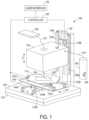
- FIG. 1depicts an additive manufacturing system that operates a liquid metal drop ejector to adjust operation of the ejector(s) in the printer to form conductive metal traces on substrates with dimensions within appropriate tolerances and with sufficient conductive material to carry electrical currents without burning up or becoming too hot.
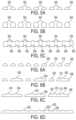
- FIG. 2 A to FIG. 2 Fare illustrations of aluminum structures formed on a polyimide substrate formed by the system of FIG. 1 when operated in the frequency and overlap ranges shown in FIG. 3 .
- FIG. 4 A and FIG. 4 Bare cross-sectional views of uniform structures of FIG. 2 E at different overlap percentages.
- FIG. 5 A to FIG. 5 Cdepict different ejection patterns for forming aluminum metal traces on semiconductor wafers.
- FIG. 6 A to FIG. 6 Ddepict different ejection patterns for forming aluminum metal traces on semiconductor wafers.
- FIG. 7 Ais an illustration of an elevated portion of a metal trace formed for connection to a lead on an electronic component on a substrate.
- FIG. 7 Bdepicts lifted traces, such as those shown in FIG. 7 A , being connected to an integrated circuit component.
- FIG. 8is a flow diagram for a process for operating the system of FIG. 1 to form metal traces on different types of material substrates.
- FIG. 1illustrates an embodiment of a melted metal 3D object printer 100 that adjusts operation of the ejector(s) in the printer to form conductive metal traces on different types of substrates with dimensions that are within appropriate tolerances and with sufficient conductive material to carry electrical currents without burning up or becoming too hot.
- drops of melted bulk metalare ejected from a printhead 104 having one or more ejectors and these drops form metal traces on a substrate 108 laying on a platform 112 .
- a source of bulk metal 160such as metal wire 130 , is fed into the printhead and melted to provide melted metal for a chamber within the printhead.
- An inert gas supply 164provides a pressure regulated source of an inert gas 168 , such as argon, to the melted metal in the printhead 104 through a gas supply tube 144 to prevent the formation of aluminum oxide in the printhead.
- the printhead 104is movably mounted within z-axis tracks 116 A and 116 B in a pair of vertically oriented members 120 A and 120 B, respectively.
- Members 120 A and 120 Bare connected at one end to one side of a frame 124 and at another end to one another by a horizontal member 128 .
- An actuator 132is mounted to the horizontal member 128 and operatively connected to the printhead 104 to move the printhead along the z-axis tracks 116 A and 116 B.
- the actuator 132is operated by a controller 136 to maintain a predetermined distance between one or more nozzles (not shown in FIG. 1 ) of the printhead 104 and an uppermost surface of the substrate 108 on the platform 112 and the traces being built on the substrate 108 .
- a planar member 140which can be formed of granite or other sturdy material to provide reliably solid support for movement of the platform 112 .
- Platform 112is affixed to X-axis tracks 144 A and 144 B so the platform 112 can move bidirectionally along an X-axis as shown in the figure.
- the X-axis tracks 144 A and 144 Bare affixed to a stage 148 and stage 148 is affixed to Y-axis tracks 152 A and 152 B so the stage 148 can move bidirectionally along a Y-axis as shown in the figure.
- Actuator 122 Ais operatively connected to the platform 112 and actuator 122 B is operatively connected to the stage 148 .
- Controller 136operates the actuators 122 A and 122 B to move the platform along the X-axis and to move the stage 148 along the Y-axis to move the platform in an X-Y plane that is opposite the printhead 104 . Performing this X-Y planar movement of platform 112 as drops of molten metal 156 are ejected toward the platform 112 forms a line of melted metal drops on the substrate 108 . Controller 136 also operates actuator 132 to adjust the vertical distance between the printhead 104 and the most recently formed layer on the substrate to facilitate formation of other structures on the substrate. While the molten metal 3D object printer 100 is depicted in FIG. 1 as being operated in a vertical orientation, other alternative orientations can be employed. Also, while the embodiment shown in FIG.
- the printhead 104can be configured for movement in the X-Y plane and along the Z axis.
- the printhead 104has only one nozzle, it is configured in other embodiments with multiple nozzles and a corresponding array of valves associated with the nozzles in a one-to-one correspondence to provide independent and selective control of the ejections from the nozzles.
- the controller 136can be implemented with one or more general or specialized programmable processors that execute programmed instructions.
- the instructions and data required to perform the programmed functionscan be stored in memory associated with the processors or controllers.
- the processors, their memories, and interface circuitryconfigure the controllers to perform the operations previously described as well as those described below.
- These componentscan be provided on a printed circuit card or provided as a circuit in an application specific integrated circuit (ASIC).
- ASICapplication specific integrated circuit
- Each of the circuitscan be implemented with a separate processor or multiple circuits can be implemented on the same processor.
- the circuitscan be implemented with discrete components or circuits provided in very large scale integrated (VLSI) circuits.
- VLSIvery large scale integrated
- circuits described hereincan be implemented with a combination of processors, ASICs, discrete components, or VLSI circuits.
- image data for a structure to be producedare sent to the processor or processors for controller 136 from either a scanning system or an online or work station connection for processing and generation of the printhead control signals output to the printhead 104 .
- the controller 136 of the melted metal 3D object printer 100requires data from external sources to control the printer for electronic device manufacture.
- a three-dimensional model or other digital data model of the device to be formedis stored in a memory operatively connected to the controller 136 , the controller can access through a server or the like a remote database in which the digital data model is stored, or a computer-readable medium in which the digital data model is stored can be selectively coupled to the controller 136 for access.
- the digital mapdepicts the circuit layout on the substrate and the locations of the leads on the electronic components to which at least some of the electrical traces are connected.
- This three-dimensional model or other digital data modelcan be used by the controller to generate machine-ready instructions for execution by the controller 136 in a known manner to operate the components of the printer 100 and form the electrical device corresponding to the model.
- the generation of the machine-ready instructionscan include the production of intermediate models, such as when a CAD model of the device is converted into an STL data model, or other polygonal mesh or other intermediate representation, which can in turn be processed to generate machine instructions, such as g-code for fabrication of the device by the printer.
- machine-ready instructionsmeans computer language commands that are executed by a computer, microprocessor, or controller to operate components of a 3D metal object additive manufacturing system to form metal structures on a substrate.
- the controller 136executes the machine-ready instructions to control the ejection of the melted metal drops from the printhead 104 , the positioning of stage 148 and the platform 112 , as well as the distance between the printhead 102 and the uppermost layer of the structures on the substrate 108 .
- the effects of metal trace formation on a substrateare a function of initial drop spacing, drop volume, the number of metal drops, the sequence and placement of drops, and the temperature at which the melted metal drops are ejected.
- the scenarios, therefore,are exemplary only and other scenarios are possible that are consistent with the principles of drop isolation, height-to-width aspect ratios, and the formation of connecting metal drops noted below.
- the behavior of metal drops on substratescan be controlled using a number of parameters that are adjustable in the printing process. These parameters include: drop frequency, spacing, temperature of the drops, and temperature of the substrate. These parameters can be used to control the metal drop freezing process and the formation of traces that are useful for electronic circuits. Various modes of metal trace formation behavior can be seen as these parameters are varied, which makes the process more or less suitable for the formation of circuit elements and conductive traces.
- Part of the digital model of the deviceidentifies the material of the substrate and the metal being fed to the printhead. Alternatively or additionally, these parameters can be entered by an operator through the user interface 170 of FIG. 1 .
- the alternating current pulses in the electromagnetic coil surrounding the printheadcan be independently varied with respect to pulse length, pulse voltage, and frequency of pulse application to provide control over the dynamics of the melted drop ejection.
- Dropsare typically ejected at a velocity of 1 to 10 meters/second, although other velocities are possible.
- nozzle orifice diameter, the distance between a nozzle orifice and the surface receiving a drop, drop temperature, substrate temperature, and drop spacingcan also affect the dynamics of melted drop ejection and interaction between the melted drops, the substrate, and the structures on the substrate.
- drop spacingmeans the distance between the centers of adjacent drops on the substrate.
- Overlap percentage(drop diameter ⁇ drop spacing)*100/drop spacing, where drop diameter is the diameter of an isolated ejected drop on a particular substrate material.
- FIG. 2 BAs the overlap percentage is increased up to about 22% and the ejection frequency is kept in the 0 Hz to 50 Hz range, a scalloped line is form ( FIG. 2 B ). At these low frequencies, the individual drop shapes remain relatively unchanged but the increase in overlap percentage results in an increased three-dimensional buildup of the line. As the ejection frequency is increased with the overlap percentage remaining in the 10% to about 22% range, the drops tend to form oblong pairs that are isolated from one another ( FIG. 2 C ). A solid metal line having bulges ( FIG. 2 D ) is formed with overlap percentages in the 23% to 70% range while ejecting the drops with a frequency in the range of about 75 Hz to about 125 Hz.
- a uniform solid metal line of about 200 ⁇ m in widthis formed using ejection frequencies in the range of about 50 Hz to about 110 Hz with the overlap percentage being in the about 30% to about 70% range ( FIG. 3 ).
- ejection frequenciesin the range of about 50 Hz to about 110 Hz with the overlap percentage being in the about 30% to about 70% range ( FIG. 3 ).
- non-planar structuresare formed ( FIG. 2 F ) when the ejection frequency is kept relative low (about 25 Hz to about 80 Hz).
- the most recently landed metal dropis still in liquid phase when the next drop that impinges on it lands so some merger occurs.
- the most recently landed metal dropis at least partially and perhaps completely solidified when the next drop lands.
- FIG. 4 Ashows a uniform structure of metal drops resembling a semicylindrical wire on the substrate when an overlap percentage of 30% is used
- FIG. 4 Bshows a uniform structure also resembling a semicylindrical wire on the substrate when an overlap percentage of 60% is used.
- the cross-sectional area of the uniform structureincreases as the overlap percentage increases. This increase in cross-sectional area occurs because the increase in overlap percentage produces a higher amount of material deposited per unit area.
- the electrical resistivity of the uniform structureswere measured and found to be in a range of about 0.9 to about 1.6 times the electrical resistance of the bulk wire fed to the printhead for melting. Electrical resistance in this range is substantially less than the electrical resistances achieved with conductive solvent inks having nanoparticles of metal.
- the metal drop ejecting printer shown in FIG. 1can be used to make conductive traces on a polyimide substrate, its use to form continuous traces on a silicon wafer or oxide layer on a silicon layer can produce adverse effects. Some of these adverse effects are thought to occur because as the trace cools, the metal trace naturally contracts more than the underlying silicon wafer. The resulting tensile strain can cause traces to delaminate from the surface or even warp thin silicon wafers.
- a method that avoids thermal warping of the silicon waferinitially ejects the isolated metal drops similar to FIG. 2 A along the intended path of the metal trace and then the gaps between the isolated drops are filled during a subsequent pass to form the continuous trace.
- the term “isolated metal drop”means a metal drop that does not touch another metal drop in either direction along a path of a conductive trace from one end of the trace to the other end.
- every other drop of the metal traceis ejected and allowed to cool for initial formation of an interrupted trace. This staggered formation of the metal trace helps reduce the thermal load on the silicon wafer to reduce substrate warping.
- the aluminumis heated to a higher drop temperature than is typical for 3D metal object formation to help the melted metal drops adhere to the semiconductor wafer.
- the aluminumis heated to 900° C. rather than a more typical range of about 700° C. to about 750° C. for this purpose.
- the ejected drop temperatureis determined empirically since the appropriate temperature range depends upon the surface properties of the substrate.
- the silicon wafermay also be heated to encourage adhesion of the melted aluminum drops to the silicon wafer.
- the printer of FIG. 1is also operated to build isolated pillars of the melted metal drops. That is, one or more additional drops are ejected onto the isolated drops initially ejected along the metal trace path to increase the aspect ratio of the height of the trace to its width. These pillars help provide sufficient metal for handling the electrical currents through the trace without subjecting the silicon wafer to a damaging thermal load. These pillars are permitted to cool before additional melted metal drops are ejected that connect the pillars to one another and complete the metal trace.
- the cooled pillarsalso act as thermal sinks for the more recently ejected drops and so significantly reduce the temperature during completion of the connected trace.
- the reduced temperaturereduces the intensity of the aluminum contraction and the stress load on the silicon or other semiconductor wafer.
- the increased height-to-width aspect of the pillars in the metal trace shown in FIG. 5 A to FIG. 5 Cprovide more surface area for dissipation of heat that is generated when large currents are passed through the trace. Multiple passes of the metal drop ejector can occur to form, in effect, aluminum walls having a height of metal drops equal to the number of passes and a width of only one metal drop.
- the drops 500are ejected along the path of the metal trace at a frequency and 0% overlap percentage so the drops are isolated from each other.
- These dropscan be sequentially printed in a single pass using a drop spacing that is large enough to provide an equidistant space between the drops.
- the thermal stress from cooling each dropis now localized and does not extend along the length of the metal trace.
- additional melted metal dropscan be printed on top of the solidified or nearly solidified isolated drops to produce pillars 504 of metal drops that are isolated from each other as shown in FIG. 5 B .
- These pillars 504provide two advantages. For one, they increase the cross-sectional area of the metal trace when it is finished to improve the electrical conductivity of the metal trace and, for another, they provide heat sinks for the ejected melted metal drops that connect the pillars to reduce the stress placed on the semiconductor substrate by the different amounts of contraction experienced by the substrate and the metal drops. These pillars 504 are then connected to one another by the metal drops 508 as shown in FIG. 5 C . The connecting metal drops 508 are ejected so they contact the pillars on each side of the metal drop and can freeze to both pillars before they reach the substrate.
- these connecting dropsmay or may not touch the substrate. Consequently, the temperature of the trace and the space between the pillars is reduced as isolated drops are connected to provide reduced stress between the trace and the substrate.
- the isolated metal drops initially ejected onto the substrate as shown in FIG. 5 Acan be connected by the subsequently ejected drops so the trace is formed with a single line of metal drops.
- This two-pass techniquestill attenuates the thermal stress on the substrate so the substrate is subjected to little or no shrinkage during the trace formation process.
- FIG. 6 A to FIG. 6 DAnother way of producing a metal trace is shown in FIG. 6 A to FIG. 6 D .
- every other metal dropis ejected onto the silicon substrate as discussed above with reference to FIG. 5 A .
- every fourth connecting metal drop 604is ejected after the first connecting metal drop is ejected into the gap between the first metal drop 608 and the second metal drop 612 as shown in FIG. 6 B .
- every fourth connecting metal drop 616is ejected after the first connecting metal drop is ejected into the gap between the second metal drop 612 and the third metal drop 620 as shown in FIG. 6 C .
- every fourth connecting metal drop 624is ejected after the first connecting metal drop is ejected into the gap between the third metal drop 620 and the fourth metal drop 628 as shown in FIG. 6 D .
- This method of printer operationforms a metal trace with a line of single metal drops without subjecting the underlying substrate with a stress that leads to the substrate warping.
- Some substratesare sufficiently robust that they can withstand the thermal stresses arising from the melted metal drops without requiring multiple passes of the ejector to form a single trace.
- multiple passes of the ejector(s) along the same trace pathare used to increase the height of the trace more quickly.
- the taller tracehas more conductive metal in it so it can handle a higher current.
- the ejector(s)form each layer of the trace with a uniform cross-section.
- molten metal droplet jetting techniquessimilar to those used to fabricate engineered lattice structures, electronic traces can be formed that lift up and off of the substrate. These techniques can also be used to produce traces that lift off of the surface around another trace so the traces can cross without electrical connection to one another. For example, successive metal drops can be ejected slightly off center from a previously ejected metal drop in a common direction with an overlap percentage of at least 70% overlap to build the height of the trace above the surface of the substrate and extend the trace in the common direction.
- the previously ejected dropsform a rising pillar that leans in the common direction so the trace is elevated above the lead of an electronic component and then subsequently ejected metal drops can connect the lead of the electronic component to the elevated metal trace.
- An example of an elevated traceis shown in FIG. 7 A .
- These lifted tracescan then be connected to circuit leads for integrated circuit components, passive components, and the like as shown in FIG. 7 B .
- FIG. 8A process for operating the printer shown in FIG. 1 is shown in FIG. 8 .
- statements that the process is performing some task or functionrefers to a controller or general purpose processor executing programmed instructions stored in non-transitory computer readable storage media operatively connected to the controller or processor to manipulate data or to operate one or more components in the printer to perform the task or function.
- the controller 136 noted abovecan be such a controller or processor.
- the controllercan be implemented with more than one processor and associated circuitry and components, each of which is configured to form one or more tasks or functions described herein.
- the steps of the methodmay be performed in any feasible chronological order, regardless of the order shown in the figures or the order in which the processing is described.
- FIG. 8is a flow diagram of a process 800 that operates the printing system 10 to adjust operation of the ejector(s) in the printer to form an electronic device having conductive metal traces on substrates with dimensions within appropriate tolerances and with sufficient conductive material to carry electrical currents without burning up or becoming too hot.
- the process 800begins with detection of a metal trace within a three-dimensional digital model of an electrical circuit (block 804 ). The process then identifies the bulk metal being melted and the material of the substrate onto which the melted bulk metal is ejected (block 808 ). This identification can occur from data in the digital model of the electronic device being formed or from the user interface. The process then selects operational parameters for forming the metal trace (block 812 ).
- These operational parametersinclude an ejection frequency, an overlap percentage, a melting temperature for the bulk metal, one or more patterns for the trace formation, a height-to-width aspect ratio, and the like. These operational parameters are then used to operate the system to form the metal trace on the substrate including connecting the trace to electronic component leads, if necessary (block 816 ). This process continues (block 820 ) until the electronic device has been formed.
Landscapes
- Engineering & Computer Science (AREA)
- Chemical & Material Sciences (AREA)
- Materials Engineering (AREA)
- Manufacturing & Machinery (AREA)
- Mechanical Engineering (AREA)
- Composite Materials (AREA)
- Physics & Mathematics (AREA)
- Optics & Photonics (AREA)
- Automation & Control Theory (AREA)
- Analytical Chemistry (AREA)
- Manufacturing Of Printed Wiring (AREA)
- Powder Metallurgy (AREA)
Abstract
Description
Claims (10)
Priority Applications (2)
| Application Number | Priority Date | Filing Date | Title |
|---|---|---|---|
| US18/321,509US12186992B2 (en) | 2020-07-31 | 2023-05-22 | Method for operating a metal drop ejecting three-dimensional (3D) object printer to form electrical circuits on substrates |
| US18/788,666US20240383210A1 (en) | 2020-07-31 | 2024-07-30 | Method for operating a metal drop ejecting three-dimensional (3d) object printer to form electrical circuits on substrates |
Applications Claiming Priority (2)
| Application Number | Priority Date | Filing Date | Title |
|---|---|---|---|
| US16/945,509US11731366B2 (en) | 2020-07-31 | 2020-07-31 | Method and system for operating a metal drop ejecting three-dimensional (3D) object printer to form electrical circuits on substrates |
| US18/321,509US12186992B2 (en) | 2020-07-31 | 2023-05-22 | Method for operating a metal drop ejecting three-dimensional (3D) object printer to form electrical circuits on substrates |
Related Parent Applications (2)
| Application Number | Title | Priority Date | Filing Date |
|---|---|---|---|
| US16/549,509DivisionUS11022995B2 (en) | 2007-08-28 | 2019-08-23 | Method and apparatus for actively managing consumption of electric power over an electric power grid |
| US16/945,509DivisionUS11731366B2 (en) | 2020-07-31 | 2020-07-31 | Method and system for operating a metal drop ejecting three-dimensional (3D) object printer to form electrical circuits on substrates |
Related Child Applications (1)
| Application Number | Title | Priority Date | Filing Date |
|---|---|---|---|
| US18/788,666ContinuationUS20240383210A1 (en) | 2020-07-31 | 2024-07-30 | Method for operating a metal drop ejecting three-dimensional (3d) object printer to form electrical circuits on substrates |
Publications (2)
| Publication Number | Publication Date |
|---|---|
| US20230294364A1 US20230294364A1 (en) | 2023-09-21 |
| US12186992B2true US12186992B2 (en) | 2025-01-07 |
Family
ID=76744618
Family Applications (3)
| Application Number | Title | Priority Date | Filing Date |
|---|---|---|---|
| US16/945,509Active2041-04-09US11731366B2 (en) | 2020-07-31 | 2020-07-31 | Method and system for operating a metal drop ejecting three-dimensional (3D) object printer to form electrical circuits on substrates |
| US18/321,509ActiveUS12186992B2 (en) | 2020-07-31 | 2023-05-22 | Method for operating a metal drop ejecting three-dimensional (3D) object printer to form electrical circuits on substrates |
| US18/788,666PendingUS20240383210A1 (en) | 2020-07-31 | 2024-07-30 | Method for operating a metal drop ejecting three-dimensional (3d) object printer to form electrical circuits on substrates |
Family Applications Before (1)
| Application Number | Title | Priority Date | Filing Date |
|---|---|---|---|
| US16/945,509Active2041-04-09US11731366B2 (en) | 2020-07-31 | 2020-07-31 | Method and system for operating a metal drop ejecting three-dimensional (3D) object printer to form electrical circuits on substrates |
Family Applications After (1)
| Application Number | Title | Priority Date | Filing Date |
|---|---|---|---|
| US18/788,666PendingUS20240383210A1 (en) | 2020-07-31 | 2024-07-30 | Method for operating a metal drop ejecting three-dimensional (3d) object printer to form electrical circuits on substrates |
Country Status (5)
| Country | Link |
|---|---|
| US (3) | US11731366B2 (en) |
| EP (1) | EP3944912A1 (en) |
| JP (1) | JP2022027546A (en) |
| KR (1) | KR20220015955A (en) |
| CN (1) | CN114054779A (en) |
Families Citing this family (4)
| Publication number | Priority date | Publication date | Assignee | Title |
|---|---|---|---|---|
| US11737216B2 (en)* | 2021-01-22 | 2023-08-22 | Xerox Corporation | Metal drop ejecting three-dimensional (3D) object printer |
| US11794255B2 (en)* | 2021-01-27 | 2023-10-24 | Xerox Corporation | Method and apparatus for forming overhang structures with a metal drop ejecting three-dimensional (3D) object printer |
| US20240367369A1 (en)* | 2021-08-26 | 2024-11-07 | Carnegie Mellon University | Freeform Fabrication of Three-Dimensional Structures Using a Droplet-On-Demand Process With Continuous and Frequency Modulated Material Deposition |
| US20230278104A1 (en)* | 2022-03-02 | 2023-09-07 | Xerox Corporation | System and method for controlling temperature in a three-dimensional (3d) printer |
Citations (47)
| Publication number | Priority date | Publication date | Assignee | Title |
|---|---|---|---|---|
| US4832911A (en) | 1986-09-18 | 1989-05-23 | Alcan International Limited | Method of alloying aluminium |
| US6129872A (en) | 1998-08-29 | 2000-10-10 | Jang; Justin | Process and apparatus for creating a colorful three-dimensional object |
| US6238613B1 (en) | 1999-07-14 | 2001-05-29 | Stratasys, Inc. | Apparatus and method for thermoplastic extrusion |
| US6593053B1 (en) | 2000-10-23 | 2003-07-15 | Xerox Corporation | Method for controlling melt rheology of resin mixtures |
| US20040141018A1 (en) | 2003-01-16 | 2004-07-22 | Kia Silverbrook | 3-d product printing system |
| US6773249B1 (en) | 1998-03-05 | 2004-08-10 | Mauser-Werke Gmbh | Extrusion head |
| US20040164436A1 (en) | 2003-01-21 | 2004-08-26 | University Of Southern California | Multi-nozzle assembly for extrusion of wall |
| US20040253365A1 (en) | 2001-08-23 | 2004-12-16 | Warren William L. | Architecture tool and methods of use |
| US7604470B2 (en) | 2006-04-03 | 2009-10-20 | Stratasys, Inc. | Single-motor extrusion head having multiple extrusion lines |
| US7765949B2 (en) | 2005-11-17 | 2010-08-03 | Palo Alto Research Center Incorporated | Extrusion/dispensing systems and methods |
| US20140039659A1 (en) | 2012-07-31 | 2014-02-06 | Makerbot Industries, Llc | Fabrication of objects with enhanced structural characteristics |
| US20140048969A1 (en) | 2012-08-16 | 2014-02-20 | Stratasys, Inc. | Print head nozzle for use with additive manufacturing system |
| US20140121813A1 (en) | 2012-10-29 | 2014-05-01 | Makerbot Industries, Llc | Three-dimensional fabrication with cavity filling |
| US8801415B2 (en) | 2005-01-21 | 2014-08-12 | University Of Southern California | Contour crafting extrusion nozzles |
| US20140242208A1 (en) | 2013-02-27 | 2014-08-28 | CEL Technology Limited | Fluid-dispensing head for a 3d printer |
| US8827684B1 (en) | 2013-12-23 | 2014-09-09 | Radiant Fabrication | 3D printer and printhead unit with multiple filaments |
| US20140291886A1 (en) | 2013-03-22 | 2014-10-02 | Gregory Thomas Mark | Three dimensional printing |
| US20140328964A1 (en) | 2013-03-22 | 2014-11-06 | Markforged, Inc. | Three dimensional printing |
| US20140363532A1 (en) | 2013-06-10 | 2014-12-11 | Kirk W. Wolfgram | Multiple color extrusion type three dimensional printer |
| US20140368568A1 (en) | 2012-02-29 | 2014-12-18 | Fujifilm Corporation | Liquid ejection apparatus, nanoimprint system, and liquid ejection method |
| WO2014200595A2 (en) | 2013-03-15 | 2014-12-18 | 3D Systems, Inc. | Direct writing for additive manufacturing systems |
| US20150035198A1 (en) | 2013-07-31 | 2015-02-05 | Simon SABA | Systems and methods for three-dimensional printing |
| US20150056432A1 (en) | 2013-08-26 | 2015-02-26 | Palo Alto Research Center Incorporated | Co-extrusion of periodically modulated structures |
| WO2015027938A1 (en) | 2013-08-28 | 2015-03-05 | CEL Technology Limited | Desktop robot |
| US20150077215A1 (en) | 2012-04-26 | 2015-03-19 | Northeastern University | Device and Method to Additively Fabricate Structures Containing Embedded Electronics or Sensors |
| US20150093468A1 (en) | 2012-04-19 | 2015-04-02 | Construction Research And Technology Gmbh | Apparatus And System For Expanding Expandable Polymeric Microspheres |
| WO2015077262A1 (en) | 2013-11-19 | 2015-05-28 | Guill Tool & Engineering | Coextruded, multilayered and multicomponent 3d printing inputs |
| US20160136897A1 (en) | 2014-11-14 | 2016-05-19 | Cole Nielsen-Cole | Additive manufacturing techniques and systems to form composite materials |
| CN105618756A (en) | 2015-08-25 | 2016-06-01 | 国家电网公司 | Device for realizing 3D metal printing by virtue of supporting structure |
| US20160318130A1 (en) | 2011-03-31 | 2016-11-03 | Norsk Titanium As | Method and arrangement for building metallic objects by solid freeform fabrication |
| US20160325498A1 (en) | 2015-05-04 | 2016-11-10 | Daniel Gelbart | 3D Printer Based on a Staggered Nozzle Array |
| US20160346997A1 (en) | 2014-02-10 | 2016-12-01 | President And Fellows Of Harvard College | Three-dimensional (3d) printed composite structure and 3d printable composite ink formulation |
| EP3117892A1 (en) | 2014-02-24 | 2017-01-18 | Coway Co., Ltd. | Water treatment apparatus |
| CN106475564A (en)* | 2015-08-31 | 2017-03-08 | 许昌学院 | Metal drop prints 3D surface quality of workpieces control device and method |
| US20170157828A1 (en) | 2015-12-08 | 2017-06-08 | Xerox Corporation | Three-dimensional object printer with multi-nozzle extruders and dispensers for multi-nozzle extruders and printheads |
| US20170157831A1 (en) | 2015-12-08 | 2017-06-08 | Xerox Corporation | System and method for operation of multi-nozzle extrusion printheads in three-dimensional object printers |
| US20170157844A1 (en) | 2015-12-08 | 2017-06-08 | Xerox Corporation | Extrusion printheads for three-dimensional object printers |
| US20170157843A1 (en) | 2015-12-08 | 2017-06-08 | Xerox Corporation | Material feeder for engineering polymer ejection system for additive manufacturing applications |
| US20170217089A1 (en) | 2014-09-26 | 2017-08-03 | Stratasys, Inc. | Liquefier assemblies for additive manufacturing systems, and methods of use thereof |
| US9757900B2 (en) | 2015-05-20 | 2017-09-12 | Xerox Corporation | Pin-actuated printhead |
| US20170334137A1 (en) | 2016-05-17 | 2017-11-23 | Xerox Corporation | Interlayer adhesion in a part printed by additive manufacturing |
| US20180111306A1 (en) | 2016-10-26 | 2018-04-26 | Xerox Corporation | Constant pressure filament driver for extruder heads in three-dimensional object printers |
| US20180111308A1 (en) | 2016-10-26 | 2018-04-26 | Xerox Corporation | Filament heaters configured to facilitate thermal treatment of filaments for extruder heads in three-dimensional object printers |
| US20180111336A1 (en) | 2016-10-26 | 2018-04-26 | Xerox Corporation | Method of operating extruder heads in three-dimensional object printers |
| US20180126632A1 (en)* | 2015-05-14 | 2018-05-10 | Developa2 Ltd | Additive manufacturing apparatus and method |
| US9993964B2 (en) | 2016-07-14 | 2018-06-12 | Xerox Corporation | Method and system for producing three-dimensional build objects |
| US20210380032A1 (en) | 2020-06-09 | 2021-12-09 | Sean Seymour | Portable cargo strap storage device |
Family Cites Families (4)
| Publication number | Priority date | Publication date | Assignee | Title |
|---|---|---|---|---|
| US10315247B2 (en) | 2015-09-24 | 2019-06-11 | Markforged, Inc. | Molten metal jetting for additive manufacturing |
| US20170252824A1 (en) | 2016-03-03 | 2017-09-07 | Desktop Metal, Inc. | Controlling quiescent operation of magnetohydrodynamic systems for metal manufacturing |
| CA3076753A1 (en) | 2017-10-01 | 2019-04-04 | Space Foundry Inc. | Modular print head assembly for plasma jet printing |
| GB201819982D0 (en)* | 2018-12-07 | 2019-01-23 | Uea Enterprises Ltd | Inkjet printing of conductive traces |
- 2020
- 2020-07-31USUS16/945,509patent/US11731366B2/enactiveActive
- 2021
- 2021-06-30EPEP21182997.3Apatent/EP3944912A1/enactivePending
- 2021-06-30CNCN202110732156.9Apatent/CN114054779A/enactivePending
- 2021-07-21JPJP2021120199Apatent/JP2022027546A/enactivePending
- 2021-07-26KRKR1020210097489Apatent/KR20220015955A/ennot_activeWithdrawn
- 2023
- 2023-05-22USUS18/321,509patent/US12186992B2/enactiveActive
- 2024
- 2024-07-30USUS18/788,666patent/US20240383210A1/enactivePending
Patent Citations (47)
| Publication number | Priority date | Publication date | Assignee | Title |
|---|---|---|---|---|
| US4832911A (en) | 1986-09-18 | 1989-05-23 | Alcan International Limited | Method of alloying aluminium |
| US6773249B1 (en) | 1998-03-05 | 2004-08-10 | Mauser-Werke Gmbh | Extrusion head |
| US6129872A (en) | 1998-08-29 | 2000-10-10 | Jang; Justin | Process and apparatus for creating a colorful three-dimensional object |
| US6238613B1 (en) | 1999-07-14 | 2001-05-29 | Stratasys, Inc. | Apparatus and method for thermoplastic extrusion |
| US6593053B1 (en) | 2000-10-23 | 2003-07-15 | Xerox Corporation | Method for controlling melt rheology of resin mixtures |
| US20040253365A1 (en) | 2001-08-23 | 2004-12-16 | Warren William L. | Architecture tool and methods of use |
| US20040141018A1 (en) | 2003-01-16 | 2004-07-22 | Kia Silverbrook | 3-d product printing system |
| US20040164436A1 (en) | 2003-01-21 | 2004-08-26 | University Of Southern California | Multi-nozzle assembly for extrusion of wall |
| US8801415B2 (en) | 2005-01-21 | 2014-08-12 | University Of Southern California | Contour crafting extrusion nozzles |
| US7765949B2 (en) | 2005-11-17 | 2010-08-03 | Palo Alto Research Center Incorporated | Extrusion/dispensing systems and methods |
| US7604470B2 (en) | 2006-04-03 | 2009-10-20 | Stratasys, Inc. | Single-motor extrusion head having multiple extrusion lines |
| US20160318130A1 (en) | 2011-03-31 | 2016-11-03 | Norsk Titanium As | Method and arrangement for building metallic objects by solid freeform fabrication |
| US20140368568A1 (en) | 2012-02-29 | 2014-12-18 | Fujifilm Corporation | Liquid ejection apparatus, nanoimprint system, and liquid ejection method |
| US20150093468A1 (en) | 2012-04-19 | 2015-04-02 | Construction Research And Technology Gmbh | Apparatus And System For Expanding Expandable Polymeric Microspheres |
| US20150077215A1 (en) | 2012-04-26 | 2015-03-19 | Northeastern University | Device and Method to Additively Fabricate Structures Containing Embedded Electronics or Sensors |
| US20140039659A1 (en) | 2012-07-31 | 2014-02-06 | Makerbot Industries, Llc | Fabrication of objects with enhanced structural characteristics |
| US20140048969A1 (en) | 2012-08-16 | 2014-02-20 | Stratasys, Inc. | Print head nozzle for use with additive manufacturing system |
| US20140121813A1 (en) | 2012-10-29 | 2014-05-01 | Makerbot Industries, Llc | Three-dimensional fabrication with cavity filling |
| US20140242208A1 (en) | 2013-02-27 | 2014-08-28 | CEL Technology Limited | Fluid-dispensing head for a 3d printer |
| WO2014200595A2 (en) | 2013-03-15 | 2014-12-18 | 3D Systems, Inc. | Direct writing for additive manufacturing systems |
| US20140328964A1 (en) | 2013-03-22 | 2014-11-06 | Markforged, Inc. | Three dimensional printing |
| US20140291886A1 (en) | 2013-03-22 | 2014-10-02 | Gregory Thomas Mark | Three dimensional printing |
| US20140363532A1 (en) | 2013-06-10 | 2014-12-11 | Kirk W. Wolfgram | Multiple color extrusion type three dimensional printer |
| US20150035198A1 (en) | 2013-07-31 | 2015-02-05 | Simon SABA | Systems and methods for three-dimensional printing |
| US20150056432A1 (en) | 2013-08-26 | 2015-02-26 | Palo Alto Research Center Incorporated | Co-extrusion of periodically modulated structures |
| WO2015027938A1 (en) | 2013-08-28 | 2015-03-05 | CEL Technology Limited | Desktop robot |
| WO2015077262A1 (en) | 2013-11-19 | 2015-05-28 | Guill Tool & Engineering | Coextruded, multilayered and multicomponent 3d printing inputs |
| US8827684B1 (en) | 2013-12-23 | 2014-09-09 | Radiant Fabrication | 3D printer and printhead unit with multiple filaments |
| US20160346997A1 (en) | 2014-02-10 | 2016-12-01 | President And Fellows Of Harvard College | Three-dimensional (3d) printed composite structure and 3d printable composite ink formulation |
| EP3117892A1 (en) | 2014-02-24 | 2017-01-18 | Coway Co., Ltd. | Water treatment apparatus |
| US20170217089A1 (en) | 2014-09-26 | 2017-08-03 | Stratasys, Inc. | Liquefier assemblies for additive manufacturing systems, and methods of use thereof |
| US20160136897A1 (en) | 2014-11-14 | 2016-05-19 | Cole Nielsen-Cole | Additive manufacturing techniques and systems to form composite materials |
| US20160325498A1 (en) | 2015-05-04 | 2016-11-10 | Daniel Gelbart | 3D Printer Based on a Staggered Nozzle Array |
| US20180126632A1 (en)* | 2015-05-14 | 2018-05-10 | Developa2 Ltd | Additive manufacturing apparatus and method |
| US9757900B2 (en) | 2015-05-20 | 2017-09-12 | Xerox Corporation | Pin-actuated printhead |
| CN105618756A (en) | 2015-08-25 | 2016-06-01 | 国家电网公司 | Device for realizing 3D metal printing by virtue of supporting structure |
| CN106475564A (en)* | 2015-08-31 | 2017-03-08 | 许昌学院 | Metal drop prints 3D surface quality of workpieces control device and method |
| US20170157831A1 (en) | 2015-12-08 | 2017-06-08 | Xerox Corporation | System and method for operation of multi-nozzle extrusion printheads in three-dimensional object printers |
| US20170157843A1 (en) | 2015-12-08 | 2017-06-08 | Xerox Corporation | Material feeder for engineering polymer ejection system for additive manufacturing applications |
| US20170157844A1 (en) | 2015-12-08 | 2017-06-08 | Xerox Corporation | Extrusion printheads for three-dimensional object printers |
| US20170157828A1 (en) | 2015-12-08 | 2017-06-08 | Xerox Corporation | Three-dimensional object printer with multi-nozzle extruders and dispensers for multi-nozzle extruders and printheads |
| US20170334137A1 (en) | 2016-05-17 | 2017-11-23 | Xerox Corporation | Interlayer adhesion in a part printed by additive manufacturing |
| US9993964B2 (en) | 2016-07-14 | 2018-06-12 | Xerox Corporation | Method and system for producing three-dimensional build objects |
| US20180111306A1 (en) | 2016-10-26 | 2018-04-26 | Xerox Corporation | Constant pressure filament driver for extruder heads in three-dimensional object printers |
| US20180111308A1 (en) | 2016-10-26 | 2018-04-26 | Xerox Corporation | Filament heaters configured to facilitate thermal treatment of filaments for extruder heads in three-dimensional object printers |
| US20180111336A1 (en) | 2016-10-26 | 2018-04-26 | Xerox Corporation | Method of operating extruder heads in three-dimensional object printers |
| US20210380032A1 (en) | 2020-06-09 | 2021-12-09 | Sean Seymour | Portable cargo strap storage device |
Non-Patent Citations (9)
| Title |
|---|
| 3ders.org; New 3-way extruder and color blending nozzle developed for multi-colour/material 3D printing; 3D Printing Technology; Aug. 25, 2012; 11 Pages; www.3ders.org. |
| e3d-online.com; Multi-Extrusion; E3D-ONLINE; 2014; 6 Pages; www.e3d-online.com/Multi-Extrusion. |
| Francis X. Govers III; Diamond Hotend makes multi-color 3D printing possible from a single nozzle; Gizmag; Apr. 12, 2015; 6 Pages; www.gizmag.com. |
| Isaac Budmen; Understanding Shells, Layer Height and Infill; Team Budmen; Sep. 2013; 1 Page; www.blog.teambudmen.com. |
| Nscrypt, Inc.; World-wide Leader in Micro to Pico-liter Dispensing Systems with our Patented Micro Dispense Pump; nScrypt, Inc.; 2001-2012; 3 Pages; www.nscrypt.com. |
| Simplify 3D; Printing with Multiple Extruders; Jul. 23, 2015; 5 Pages; www.simplify3d.com/support/tutorials. |
| Sure Tack Systems; Automatic Adhesive Applicator Equipment; Brochure; 2018; 3 Pages; https://suretacksystems.com/products/automatic-applicators/. |
| Sure Tack Systems; HA2 Series Extrusion Hot Melt Applicator; Brochure; 2018; 4 Pages; https://suretacksystems.com/extrusion. |
| Trlica C., et al., "3-D Printing of liquid metals for stretchable and flexible conductors", Proceedings of SPIE, IEEE, US, vol. 9083, Jun. 4, 2014 (10 Pages) (Year: 2014).* |
Also Published As
| Publication number | Publication date |
|---|---|
| US11731366B2 (en) | 2023-08-22 |
| KR20220015955A (en) | 2022-02-08 |
| CN114054779A (en) | 2022-02-18 |
| US20230294364A1 (en) | 2023-09-21 |
| US20220032550A1 (en) | 2022-02-03 |
| EP3944912A1 (en) | 2022-02-02 |
| JP2022027546A (en) | 2022-02-10 |
| US20240383210A1 (en) | 2024-11-21 |
Similar Documents
| Publication | Publication Date | Title |
|---|---|---|
| US12186992B2 (en) | Method for operating a metal drop ejecting three-dimensional (3D) object printer to form electrical circuits on substrates | |
| CN104028761B (en) | The micro-spray fusing of a kind of metal drips electromagnetic confinement deposition modeling system | |
| US12439525B2 (en) | Method for operating a metal drop ejecting three-dimensional (3D) object printer to form vias in printed circuit boards with conductive metal | |
| US20210252589A1 (en) | Method and apparatus for additive manufacturing of a component | |
| US20230173585A1 (en) | Metal drop ejecting three-dimensional (3d) object printer and method of operation for forming metal support structures | |
| EP4023369B1 (en) | Metal drop ejecting three-dimensional (3d) object printer having an increased material deposition rate | |
| EP4035805A1 (en) | Method and apparatus for forming overhang structures with a metal drop ejecting three-dimensional (3d) object printer | |
| US20220226888A1 (en) | Method and system for operating a metal drop ejecting three-dimensional (3d) object printer to shorten object formation time | |
| US12109656B2 (en) | Metal drop ejecting three-dimensional (3D) object printer and method of operation for forming metal support structures | |
| US11760028B2 (en) | System and method for calibrating lag time in a three-dimensional object printer | |
| CN113458414B (en) | Method and modular heater for three-dimensional metal object fabrication system | |
| US20240207925A1 (en) | Method of operating a metal drop ejecting three-dimensional (3d) object printer to form metal support structures | |
| US11890674B2 (en) | Metal drop ejecting three-dimensional (3D) object printer and method of operation for forming support structures in 3D metal objects | |
| CN101623954A (en) | Collective transfer ink jet nozzle plate and method for manufacturing the same | |
| US20230150026A1 (en) | Metal drop ejecting three-dimensional (3d) object printer and improved method for operating the printer | |
| CN115703154A (en) | Metal droplet jetting three-dimensional (3D) object printer and method of operation for forming metal support structures | |
| US20250135541A1 (en) | System for heating objects during manufacture by a metal hybrid manufacturing system | |
| US20240042524A1 (en) | Leveraging printing standoff distance in three-dimensional printing to enhance part separation and system and methods thereof | |
| US20250135540A1 (en) | Method and system for operating a metal hybrid manufacturing system to shorten object formation time | |
| US20230271252A1 (en) | Metal drop ejecting three-dimensional (3d) object printer and method of operation for building support structures |
Legal Events
| Date | Code | Title | Description |
|---|---|---|---|
| FEPP | Fee payment procedure | Free format text:ENTITY STATUS SET TO UNDISCOUNTED (ORIGINAL EVENT CODE: BIG.); ENTITY STATUS OF PATENT OWNER: LARGE ENTITY | |
| STPP | Information on status: patent application and granting procedure in general | Free format text:DOCKETED NEW CASE - READY FOR EXAMINATION | |
| AS | Assignment | Owner name:JEFFERIES FINANCE LLC, AS COLLATERAL AGENT, NEW YORK Free format text:SECURITY INTEREST;ASSIGNOR:XEROX CORPORATION;REEL/FRAME:065628/0019 Effective date:20231117 | |
| AS | Assignment | Owner name:ADDITIVE TECHNOLOGIES LLC, FLORIDA Free format text:ASSIGNMENT OF ASSIGNORS INTEREST;ASSIGNOR:ELEM ADDITIVE, LLC;REEL/FRAME:065743/0267 Effective date:20231001 Owner name:ELEM ADDITIVE, LLC, NORTH CAROLINA Free format text:ASSIGNMENT OF ASSIGNORS INTEREST;ASSIGNOR:XEROX CORPORATION;REEL/FRAME:065734/0413 Effective date:20230811 | |
| STPP | Information on status: patent application and granting procedure in general | Free format text:NON FINAL ACTION MAILED | |
| AS | Assignment | Owner name:CITIBANK, N.A., AS COLLATERAL AGENT, NEW YORK Free format text:SECURITY INTEREST;ASSIGNOR:XEROX CORPORATION;REEL/FRAME:066741/0001 Effective date:20240206 | |
| STPP | Information on status: patent application and granting procedure in general | Free format text:RESPONSE TO NON-FINAL OFFICE ACTION ENTERED AND FORWARDED TO EXAMINER | |
| STPP | Information on status: patent application and granting procedure in general | Free format text:FINAL REJECTION MAILED | |
| STPP | Information on status: patent application and granting procedure in general | Free format text:RESPONSE AFTER FINAL ACTION FORWARDED TO EXAMINER | |
| STPP | Information on status: patent application and granting procedure in general | Free format text:NOTICE OF ALLOWANCE MAILED -- APPLICATION RECEIVED IN OFFICE OF PUBLICATIONS | |
| STPP | Information on status: patent application and granting procedure in general | Free format text:PUBLICATIONS -- ISSUE FEE PAYMENT RECEIVED | |
| STPP | Information on status: patent application and granting procedure in general | Free format text:PUBLICATIONS -- ISSUE FEE PAYMENT VERIFIED | |
| STCF | Information on status: patent grant | Free format text:PATENTED CASE |