US12184159B2 - Solar power generation system - Google Patents
Solar power generation systemDownload PDFInfo
- Publication number
- US12184159B2 US12184159B2US17/589,097US202217589097AUS12184159B2US 12184159 B2US12184159 B2US 12184159B2US 202217589097 AUS202217589097 AUS 202217589097AUS 12184159 B2US12184159 B2US 12184159B2
- Authority
- US
- United States
- Prior art keywords
- power
- deadband
- modules
- grid
- waveform
- Prior art date
- Legal status (The legal status is an assumption and is not a legal conclusion. Google has not performed a legal analysis and makes no representation as to the accuracy of the status listed.)
- Active
Links
Images


Classifications
- H—ELECTRICITY
- H02—GENERATION; CONVERSION OR DISTRIBUTION OF ELECTRIC POWER
- H02M—APPARATUS FOR CONVERSION BETWEEN AC AND AC, BETWEEN AC AND DC, OR BETWEEN DC AND DC, AND FOR USE WITH MAINS OR SIMILAR POWER SUPPLY SYSTEMS; CONVERSION OF DC OR AC INPUT POWER INTO SURGE OUTPUT POWER; CONTROL OR REGULATION THEREOF
- H02M1/00—Details of apparatus for conversion
- H02M1/0067—Converter structures employing plural converter units, other than for parallel operation of the units on a single load
- H02M1/007—Plural converter units in cascade
- H01L31/02021—
- H—ELECTRICITY
- H02—GENERATION; CONVERSION OR DISTRIBUTION OF ELECTRIC POWER
- H02J—CIRCUIT ARRANGEMENTS OR SYSTEMS FOR SUPPLYING OR DISTRIBUTING ELECTRIC POWER; SYSTEMS FOR STORING ELECTRIC ENERGY
- H02J3/00—Circuit arrangements for AC mains or AC distribution networks
- H02J3/38—Arrangements for parallely feeding a single network by two or more generators, converters or transformers
- H02J3/381—Dispersed generators
- H—ELECTRICITY
- H02—GENERATION; CONVERSION OR DISTRIBUTION OF ELECTRIC POWER
- H02J—CIRCUIT ARRANGEMENTS OR SYSTEMS FOR SUPPLYING OR DISTRIBUTING ELECTRIC POWER; SYSTEMS FOR STORING ELECTRIC ENERGY
- H02J3/00—Circuit arrangements for AC mains or AC distribution networks
- H02J3/38—Arrangements for parallely feeding a single network by two or more generators, converters or transformers
- H02J3/388—Islanding, i.e. disconnection of local power supply from the network
- H—ELECTRICITY
- H02—GENERATION; CONVERSION OR DISTRIBUTION OF ELECTRIC POWER
- H02J—CIRCUIT ARRANGEMENTS OR SYSTEMS FOR SUPPLYING OR DISTRIBUTING ELECTRIC POWER; SYSTEMS FOR STORING ELECTRIC ENERGY
- H02J7/00—Circuit arrangements for charging or depolarising batteries or for supplying loads from batteries
- H02J7/34—Parallel operation in networks using both storage and other DC sources, e.g. providing buffering
- H02J7/35—Parallel operation in networks using both storage and other DC sources, e.g. providing buffering with light sensitive cells
- H—ELECTRICITY
- H02—GENERATION; CONVERSION OR DISTRIBUTION OF ELECTRIC POWER
- H02M—APPARATUS FOR CONVERSION BETWEEN AC AND AC, BETWEEN AC AND DC, OR BETWEEN DC AND DC, AND FOR USE WITH MAINS OR SIMILAR POWER SUPPLY SYSTEMS; CONVERSION OF DC OR AC INPUT POWER INTO SURGE OUTPUT POWER; CONTROL OR REGULATION THEREOF
- H02M1/00—Details of apparatus for conversion
- H02M1/0048—Circuits or arrangements for reducing losses
- H02M1/0054—Transistor switching losses
- H—ELECTRICITY
- H02—GENERATION; CONVERSION OR DISTRIBUTION OF ELECTRIC POWER
- H02M—APPARATUS FOR CONVERSION BETWEEN AC AND AC, BETWEEN AC AND DC, OR BETWEEN DC AND DC, AND FOR USE WITH MAINS OR SIMILAR POWER SUPPLY SYSTEMS; CONVERSION OF DC OR AC INPUT POWER INTO SURGE OUTPUT POWER; CONTROL OR REGULATION THEREOF
- H02M3/00—Conversion of DC power input into DC power output
- H02M3/02—Conversion of DC power input into DC power output without intermediate conversion into AC
- H02M3/04—Conversion of DC power input into DC power output without intermediate conversion into AC by static converters
- H02M3/10—Conversion of DC power input into DC power output without intermediate conversion into AC by static converters using discharge tubes with control electrode or semiconductor devices with control electrode
- H02M3/145—Conversion of DC power input into DC power output without intermediate conversion into AC by static converters using discharge tubes with control electrode or semiconductor devices with control electrode using devices of a triode or transistor type requiring continuous application of a control signal
- H02M3/155—Conversion of DC power input into DC power output without intermediate conversion into AC by static converters using discharge tubes with control electrode or semiconductor devices with control electrode using devices of a triode or transistor type requiring continuous application of a control signal using semiconductor devices only
- H—ELECTRICITY
- H02—GENERATION; CONVERSION OR DISTRIBUTION OF ELECTRIC POWER
- H02M—APPARATUS FOR CONVERSION BETWEEN AC AND AC, BETWEEN AC AND DC, OR BETWEEN DC AND DC, AND FOR USE WITH MAINS OR SIMILAR POWER SUPPLY SYSTEMS; CONVERSION OF DC OR AC INPUT POWER INTO SURGE OUTPUT POWER; CONTROL OR REGULATION THEREOF
- H02M7/00—Conversion of AC power input into DC power output; Conversion of DC power input into AC power output
- H02M7/42—Conversion of DC power input into AC power output without possibility of reversal
- H02M7/44—Conversion of DC power input into AC power output without possibility of reversal by static converters
- H02M7/48—Conversion of DC power input into AC power output without possibility of reversal by static converters using discharge tubes with control electrode or semiconductor devices with control electrode
- H—ELECTRICITY
- H02—GENERATION; CONVERSION OR DISTRIBUTION OF ELECTRIC POWER
- H02S—GENERATION OF ELECTRIC POWER BY CONVERSION OF INFRARED RADIATION, VISIBLE LIGHT OR ULTRAVIOLET LIGHT, e.g. USING PHOTOVOLTAIC [PV] MODULES
- H02S40/00—Components or accessories in combination with PV modules, not provided for in groups H02S10/00 - H02S30/00
- H02S40/30—Electrical components
- H02S40/32—Electrical components comprising DC/AC inverter means associated with the PV module itself, e.g. AC modules
- H—ELECTRICITY
- H02—GENERATION; CONVERSION OR DISTRIBUTION OF ELECTRIC POWER
- H02S—GENERATION OF ELECTRIC POWER BY CONVERSION OF INFRARED RADIATION, VISIBLE LIGHT OR ULTRAVIOLET LIGHT, e.g. USING PHOTOVOLTAIC [PV] MODULES
- H02S40/00—Components or accessories in combination with PV modules, not provided for in groups H02S10/00 - H02S30/00
- H02S40/30—Electrical components
- H02S40/36—Electrical components characterised by special electrical interconnection means between two or more PV modules, e.g. electrical module-to-module connection
- H—ELECTRICITY
- H10—SEMICONDUCTOR DEVICES; ELECTRIC SOLID-STATE DEVICES NOT OTHERWISE PROVIDED FOR
- H10F—INORGANIC SEMICONDUCTOR DEVICES SENSITIVE TO INFRARED RADIATION, LIGHT, ELECTROMAGNETIC RADIATION OF SHORTER WAVELENGTH OR CORPUSCULAR RADIATION
- H10F77/00—Constructional details of devices covered by this subclass
- H10F77/95—Circuit arrangements
- H10F77/953—Circuit arrangements for devices having potential barriers
- H10F77/955—Circuit arrangements for devices having potential barriers for photovoltaic devices
- H—ELECTRICITY
- H02—GENERATION; CONVERSION OR DISTRIBUTION OF ELECTRIC POWER
- H02J—CIRCUIT ARRANGEMENTS OR SYSTEMS FOR SUPPLYING OR DISTRIBUTING ELECTRIC POWER; SYSTEMS FOR STORING ELECTRIC ENERGY
- H02J2300/00—Systems for supplying or distributing electric power characterised by decentralized, dispersed, or local generation
- H02J2300/20—The dispersed energy generation being of renewable origin
- H02J2300/22—The renewable source being solar energy
- H02J2300/24—The renewable source being solar energy of photovoltaic origin
- Y—GENERAL TAGGING OF NEW TECHNOLOGICAL DEVELOPMENTS; GENERAL TAGGING OF CROSS-SECTIONAL TECHNOLOGIES SPANNING OVER SEVERAL SECTIONS OF THE IPC; TECHNICAL SUBJECTS COVERED BY FORMER USPC CROSS-REFERENCE ART COLLECTIONS [XRACs] AND DIGESTS
- Y02—TECHNOLOGIES OR APPLICATIONS FOR MITIGATION OR ADAPTATION AGAINST CLIMATE CHANGE
- Y02B—CLIMATE CHANGE MITIGATION TECHNOLOGIES RELATED TO BUILDINGS, e.g. HOUSING, HOUSE APPLIANCES OR RELATED END-USER APPLICATIONS
- Y02B70/00—Technologies for an efficient end-user side electric power management and consumption
- Y02B70/10—Technologies improving the efficiency by using switched-mode power supplies [SMPS], i.e. efficient power electronics conversion e.g. power factor correction or reduction of losses in power supplies or efficient standby modes
Definitions
- the cost per watt associated with solar power generation systemsis tied to almost all elements of the system. As just some examples, costs associated with the production and sale of solar power system components, the installation of those components, and the on-going maintenance of those components each impact the cost per watt of the overall system. Likewise, the electrical efficiency of the system in harvesting and transmitting usable power significantly impacts the cost-per-watt of the system as a whole. Innovations relating to any aspect of a solar power system that provide improvements to any or all of these cost centers can lead to reductions in system cost-per-watt. Indeed, numerous aspects of existing solar power systems—beyond solar panels themselves—are ripe for improvement.
- Solar panelsare designed to use the photovoltaic effect to convert photons emitted by the sun into direct current (DC) power.
- DCdirect current
- ACalternating current
- the DC to AC conversion of solar generated poweris conventionally accomplished by an inverter, which can implemented into a power generation system in a variety of ways.
- invertersare generally implemented into solar power generation systems with a centralized or module-level architecture.
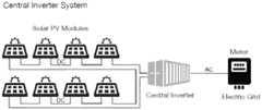
- a fully centralized configurationan example of which is shown in FIG. 1 A , a single inverter is positioned between strings of solar modules and the electric grid.
- each string of solar modulesdelivers DC power to the centralized inverter, which then converts the collectively input DC power into AC power output.
- the AC power outputis then transmitted to the grid.
- centralized inverter systemsare sometimes referred to as “string inverter” systems.
- FIG. 1 Billustrates a semi-centralized string inverter configuration using multiple inverters (as opposed to one).
- each inverteris again positioned between strings of solar modules and the electric grid.
- Each inverterconverts the DC power received from its respective string of solar modules, converts that input power to AC, and delivers the AC power—along with the other inverters—to the electric grid.
- Solar modules stringsare limited at any given time by the least productive module in the string. In other words, a given solar module string will only produce as much power as the least productive module. In environments where certain solar modules might be shaded while others are not (e.g., large strings or strings having modules facing different directions), this can significantly reduce the efficiency with which the solar modules can harvest energy. Moreover, string inverter architectures are more susceptible to losses in power generation when a solar module is damaged or otherwise not functioning properly.
- a further disadvantage of string inverter systemsis their lack of control at the solar module level.
- conventional string inverterscan only track maximum power (e.g., as part of an MPPT algorithm) down to the string level as opposed to the panel level. If there is a weak module in the string, the weakened module will limit the amount of power that can be extracted from the string of modules.
- high voltage potentialse.g., 600-2000V
- These high voltage potentialscan present a fire hazard if any of the electrical connections in the solar array become loose or damaged, which necessitates additional hardware close to the module to mitigate against this risk.
- String invertersalso have inherent inefficiencies resulting from high voltage transistors that must be used to synthesize sine waves.
- the high voltage of the solar module stringe.g., 600-2000V as noted above
- the MOSFETs and IGBTsmust switch at high frequencies, which generates more heat losses that a comparably low voltage MOSFET.
- the high voltage devicesalso require larger inductors and capacitors. As a result, string inverter systems are limited with respect to their efficiency in inverting power from solar modules.
- FIGS. 1 C and 1 Dillustrate examples of existing module-level architectures.
- FIG. 1 Cshows a micro-inverter system architecture in which inverters are provided for each solar module in the system. These “micro” inverters are typically installed on the back of modules of solar panels, integrated as part of the modules themselves, or otherwise provided proximate to the modules. Each micro-inverter is configured to convert the DC power received from its respective solar panel into AC power, which is then transmitted from the inverter to the electric grid.
- Micro-inverter architecturesare popular in residential environments where the total number of solar modules is lower. As a result, the micro-inverter architecture may in some circumstances be configured to deliver AC power harvested from various inverters directly to a building load as indicted in FIG. 1 C .
- FIG. 1 Dillustrates another module-level architecture in which DC optimizers are provided at each solar module.
- each DC optimizeris configured to condition the DC power received from its respective solar module and transmit this conditioned DC power to a string inverter provided between the optimizers and electric grid.
- the DC optimizersare provided in the system at the module-level analogously the aforementioned micro-inverters.
- module-level architecturesare popular in residential applications and other environments where less modules are used. Because of the module-level nature of these systems, they are better suited for environments susceptible to shading. In particular, both micr-inverter and DC optimizer systems allow for optimization module-by-module and, as a result, are typically more efficient than a string inverter system using the same number of modules. These module-level architectures also have a number of drawbacks and limitations.
- both micro-inverter and DC optimizer systemsare more costly than comparable string inverter systems.
- each micro-inverterrequires a full array of electronics necessary to convert DC power from solar modules into AC, including large transformers and extra transistors.
- an individual micro-inverteris provided for each solar module, increasing not only the total cost of componentry but also significantly increasing the cost and complexity of installation.
- DC optimizer systemsthe presence of optimizers themselves increases the cost of system components and installation cost.
- DC optimizer systemsstill require high voltage MOSFETs or IGBTS along with large magnetics to convert DC to AC power, thereby reducing efficiency of the overall system.
- DC electric transmission and distribution systemsare highly susceptible to arc faults, due to the nature of DC transmission. To protect against potential hazards from arc faults, including the risk of fire and the risk of electric shock, conventional DC systems require large and expensive protection equipment, such as DC-rated circuit breakers. Those working on DC systems must also wear substantial personal safety equipment for protection.
- FIGS. 1 A- 1 Dshow schematic representations of various existing solar power generation systems
- FIG. 2shows a schematic diagram of a solar power generation system having distributed power converter nodes according to one embodiment
- FIG. 3 Ashows a deadband DC waveform generated by a power converter node from the DC power received from a solar module according to one embodiment
- FIG. 3 Bshows a deadband DC waveform generated by a power converter node from the DC power received from a solar module according to another embodiment
- FIG. 4shows a power converter node according to one embodiment
- FIG. 5shows a circuit diagram of deadband converter circuit provided within a power converter node according to one embodiment
- FIG. 6shows a grid sine wave and a corresponding node synchronization signal generated by a grid interface box according to one embodiment
- FIG. 7shows a power-with-Ethernet cable according to one embodiment
- FIGS. 8 A and 8 Bshow cross-sectional and isometric cut-away views of the power-with-Ethernet cable of FIG. 7 according to one embodiment
- FIG. 9 A and 9 Bshow female and male power-with-Ethernet cable connectors, respectively, according to one embodiment
- FIG. 10shows a schematic diagram of a grid interface box (GIB) according to one embodiment
- FIG. 12illustrates a power module according to one embodiment
- FIG. 13illustrates a VAR modules according to one embodiment
- FIG. 14illustrates an aggregator module according to one embodiment
- FIG. 15shows a schematic diagram of a grid interface box having a 3-phase WYE configuration according to one embodiment
- FIG. 16shows a schematic diagram of a grid interface box having a 3-phase delta configuration according to one embodiment
- FIG. 17shows a schematic diagram of a grid interface box having a single phase configuration according to one embodiment.
- the solar power generation systemincludes a plurality of distributed power converter nodes each configured to convert DC power received from a solar module into a deadband DC waveform.
- the deadband DC power generated by each nodeis then transmitted to a centralized grid interface box (GIB) configured to unfold the deadband DC waveform into an AC signal suitable for transmission to an electric power grid.
- GEBcentralized grid interface box
- the use of distributed power converter nodes configured for producing a deadband DC waveformimproves the efficiency and cost-effectiveness of the solar power generation system. For example, as the power converter nodes do not require all of the electronics necessary to convert DC power received from a solar module in to a full AC power signal, the power converter nodes are smaller and lower-cost than existing micro-inverters. In addition, because the power converter nodes use fewer switching devices that conventional micro-inverters, they will incur less switching losses and provide improved efficiency.
- the power convertersare configured to convert DC power into a deadband DC waveform—which includes regular periods of zero-voltage dead time—the transmission of power from the power converters to the GIB presents a reduced risk of arcing, thereby improving the safety of the system as a whole.
- the distributed power converter nodesare connected to one another—and ultimately to the GIB—by power-with-Ethernet (PWE) cables and connectors.
- the power-with-Ethernet cablesare each comprised, for example, of two power conductor cables, two twisted pairs of data communication cables, and two additional untwisted data communication cables.
- PWEpower-with-Ethernet
- the inclusion of separate power and data communication cables within the PWE cableenables efficient transmission of power alongside uninterrupted data communication.
- the use of PWE cables in the solar generation systemenables quick and efficient power converter node synchronization.
- Most distributed architecturesuse either wireless RF communication or Power Line Carrier Communication (PLCC).
- PLCCPower Line Carrier Communication
- the PWE cableprovides a dedicated hardwired communication line between the power converter nodes and the GIB, synchronization between the power converter nodes can be performed more quickly and at a lower cost. More broadly, the use of permanent communication wires enables the power converter nodes and GIB to communicate using higher bandwidth protocols, such as Ethernet. As a result, larger amounts of data can be exchanged as compared with lower bandwidth protocols, such as PLCC. Moreover, well-defined protocols developed for the internet can be used to ensure network security across the solar power generation system.
- various embodiments of the GIB provided in the solar power generation systemare provided with a modular configuration that enables the GIB to be easily scaled for different applications.
- the GIBis provided with removable power and VAR modules, which can be added and removed into the GIB's chassis as needed in order to provide the necessary capacity for converting deadband DC power routed to the GIB into AC power suitable for supply to the grid.
- each individual GIB unitcan be used in a variety of solar power generation systems, including both small-scale (e.g., residential) and large-scale (e.g., solar farm) systems.
- FIG. 2shows a schematic diagram of a solar power generation system according to one embodiment of the present invention.
- the solar power generation systemis generally comprised of a plurality of solar modules 5 , a plurality of power converter nodes 100 , and grid interface box (GIB) 300 .
- the solar modules 5are generally configured to convert solar energy into DC power.
- the power converter nodes 100are generally configured to convert DC power received from the solar modules 5 into a deadband DC waveform, which is transmitted to the GIB 300 .
- the GIB 300is configured to unfold the deadband DC waveform transmitted by the power converter nodes 100 and output AC power suitable for supply to an electric power grid.
- the solar modules 5each comprise a plurality of solar panels configured to convert solar energy into DC power output.
- the solar modules 5are each configured to output approximately 300 watts of power at 30 volts.
- solar modules configured to output a variety of wattagescan be implemented in the present invention.
- each solar module 5is connected to a power converter node 100 by power cables 7 .
- the power cables 7may comprise PV rated cables having MC4 connectors.
- any electrical cable and connector suitable for transmitting DC power from a solar module 5 to a power converter node 100may be used.
- the solar modules 5 depicted in FIG. 2may represent a plurality of modules installed in any solar power production environment.
- the solar modules 5may represent a plurality of modules mounted on a residential home, a plurality of modules installed for powering a commercial or industrial building, or a plurality of modules forming a large scale solar power station.
- each solar module 5may be connected to an individual power converter node 100 or, in various other embodiments, multiple solar modules 5 may be connected (e.g., in series) to an individual power converter node 100 .
- the solar power generation system's power converter nodes 100are each generally configured to receive DC power generated by one or more solar modules 5 and convert the received DC power into a deadband DC waveform.
- FIG. 3 Aillustrates a deadband DC waveform 402 generated by a power converter node 100 from the DC power received from a solar module 5 according to one embodiment.
- the deadband DC waveform 402is a rectified sinewave having periods of dead time 404 —e.g., zero voltage—between the peaks of the rectified sinewave.
- the deadband DC waveform 402does not cross zero voltage.
- FIG. 3 Billustrates a deadband DC waveform 406 generated by a power converter node 100 from the DC power received from a solar module 5 according to another embodiment.
- the deadband DC waveform 406is a modified trapezoidal waveform and—like the waveform 402 —includes deadband periods 408 between its peaks.
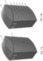
- FIG. 4illustrates a power converter node 100 according to one embodiment.
- the power converter node 100includes a housing 102 , within which the power converter's electronic components (discussed in more detail herein) are positioned.
- the housing 102includes a body portion formed with a plurality of heat dissipating fins (e.g., formed from extruded aluminum).
- the housing 102may be constructed from a thermally conductive material (e.g., metals, metal alloys, thermally conductive plastic, a combination of plastics and metals and/or the like).
- a mounting bracket 104is secured to the housing 102 .
- the mounting bracket 104is configured to enable the power converter 100 to be mounted directly to a respective solar module 5 or other surface proximate to the solar modules 5 .
- the power converter node 100includes a female electrical connector 112 and a male electrical connector 114 .
- the electrical connectors 112 , 114are input power connectors configured to be secured to power cables 7 in order to facilitate transmission of DC power generated by a solar module 5 to the power converter node 100 .
- the electrical connectors 112 , 114are MC4 connectors.
- a second end of the power converter node 100includes a second pair of male and female electrical connectors 114 , 112 (e.g., that connect to a second solar power module).
- the power converter node 100also includes at its first end a pair of female power-with-Ethernet (PWE) connectors 120 .
- the female PWE connectors 120are configured to be secured to a power-with-Ethernet cable 200 in order to provide an electrical and data communication connection between the power converter nodes 100 and the GIB 300 .
- the second end of the power converter node 100further includes a pair of male power-with-Ethernet (PWE) connectors 130 .
- the male PWE connectors 130are configured to be secured to a power-with-Ethernet cable 200 in order to provide an electrical and data communication connection between the power converter nodes 100 and the GIB 300 .
- Various features of the PWE connectors 120 , 130are described in greater detail herein with respect to FIGS. 6 - 8 .
- FIG. 5shows a circuit diagram of deadband converter circuit 160 provided within the power converter node 100 according to one embodiment.
- the deadband power converter circuit 160is a DC-DC converter disposed within the power converter node's housing 102 .
- the circuit 160includes a pair of voltage inputs 162 (positive and negative).
- the voltage inputs 162are electrically connected to one of power converter node's pairs of electrical connectors 112 , 114 .
- Power received through the voltage inputs 162is routed to a pair of switching transistors 172 , 173 , which are configured to regulate power flow through the circuit 160 .
- the circuit 160is able to transform the flat DC waveform received from a solar module 5 into a shaped DC waveform having deadbands (e.g., as shown in FIGS. 3 A and 3 B ).
- the deadband DC waveformis then output from the circuit via a pair of voltage outputs 164 (positive and negative).
- the voltage outputs 164are electrically connected to power connector contacts in one of the power converter node's PWE connectors 120 , 130 .
- the embodiment shown in FIG. 4includes two independent node circuits (e.g., of the type shown in FIG. 5 ) within the housing 102 .
- Each circuituses a set of inputs from the solar module 112 , 114 , input from a PWE connector 120 , and an output from a PWE connector 130 .
- the two circuitsare completely independent and can be connected to each other externally in either series or parallel by means of the external PWE cable 200 .
- a single loopback jumpercan be used (e.g., as shown on the second node 100 from the left in FIG. 2 ).
- two sets of jumperscan be used on both sets of connectors ( 120 , 130 ) (e.g., as shown on the second node from the right in FIG. 2 ).
- the power converter nodes 100are each rated, for example, to handle 300 W of power from each of the solar modules 5 .
- the power converter nodes 100can be configured to handle additional power (e.g., 400-800 W).
- the deadband DC waveform generated by the power converter nodes 100is configured to have deadbands 404 each having a pulse width of approximately 100 microseconds and occurring every 8.33 milliseconds (e.g., in a 60 hz signal).
- the frequency and widths of the deadbands 404can be adjusted by the transistors 172 , 173 .
- the deadbands 404can be adjusted for time length such that power transmission is optimized and, as line voltage increases, the deadband width may be increased.
- the deadband converter circuit 160is also configured to synchronize its deadband DC waveform to the electric grid.
- the solar power generation system's GIB 300is configured to monitor the sinusoidal voltage on the electric grid and identify zero crossings in the voltage (e.g., detected by a change in polarity of the monitored voltage). When a zero crossing of the grid sine wave is detected, the GIB generates a transition in either voltage or current in a synchronization wire provided in the PWE cable 200 . For example, the GIB could transition from low voltage to high voltage or high voltage to low voltage. If a current signal is utilized instead of a voltage signal, then a transition from high current to low current or vice versa is utilized. As an example, FIG. 6 illustrates an example of a grid sine wave 191 and a corresponding node synchronization signal 191 generated by the GIB 300 .
- each power converter node 100 in the systemmonitors a signal line in the PWE cable 200 for transitions.
- a transition in either voltage or currentis detected on the synchronization wire, a node 100 starts generating a rectified deadband waveform to feed to the GIB 300 .
- all of the distributed power converter nodes 100can be synchronized to the electric grid.
- the power converter node 100includes a pair of deadband converter circuits 160 .
- the voltage inputs 162 of a first circuit 160are electrically connected to a first pair of the node's electrical connectors 112 , 114
- the voltage inputs 162 of a second circuit 160are connected to the other of the node's electrical connectors 112 , 114 .
- the voltage outputs 164 of the first circuit 160are electrically connected to one of the node's PWE connectors 120 , 130
- the voltage outputs 164 of a second circuit 160are connected to the other of the PWE connectors 120 , 130 .
- the illustrated embodiment of the power converter node 100is provided with a dual-node architecture.
- the dual deadband converter circuits 160can be arranged in parallel or series via PWE cables 200 connecting the power converter nodes 100 to one another. This is shown, for example, in FIG. 2 , which—from left to right—illustrates the first three power converter nodes 100 connected in series by PWE cables 200 , while the next three power converter nodes 100 are connected in parallel.
- the PWE connectors 130can be configured as inputs from other power converter nodes 100
- the PWE connectors 120can be configured as outputs.
- FIG. 7shows a PWE cable 200 according to one embodiment.
- each PWE cable 200includes a female PWE connector 120 at one end and a male PWE connector 130 at the opposite end.
- each PWE cable 200is comprised of two power conductors, two twisted pairs of conductors for data communication, and two additional untwisted data communication conductors.
- FIGS. 8 A and 8 Billustrate cross-sectional and isometric cut-away views of the PWE cable 200 , respectively, according to one embodiment.
- the PWE cable 200includes two power conductors 202 positioned adjacent to one another, two twisted pairs of conductors for data communication 204 positioned on opposite sides of the power conductors 202 , and two additional untwisted data communication conductors 208 .
- the power conductors 202are AWG 12 7 strand copper wires coated with a protective material (e.g., PVC or HDPE insulation).
- the twisted pair data communication conductors 204 and untwisted data communication conductors 208are AWG 24 solid copper wires coated with a protective material (e.g., PVC or HDPE insulation).
- a protective materiale.g., PVC or HDPE insulation.
- the power conductors 202 , twisted pairs of data communication conductors 204 , and untwisted data communication conductors 208wrapped with a protective wrap 212 (e.g., a thin polyester wrap) and positioned within a cable jacket 210 (e.g., PVC, PE, or TPE cable jacket).
- a protective wrap 212e.g., a thin polyester wrap
- a cable jacket 210e.g., PVC, PE, or TPE cable jacket.
- the combination of cables 202 , 204 , and 208enables a round cable (e.g., as can be seen from the cross-sectional view of FIG. 8 A ).
- the PWE cable's power conductors 202are configured to transmit the deadband DC power generated by the respective power converter nodes 100 throughout the solar power generation system.
- the twisted pairs of data communication conductors 204 and untwisted data communication conductors 208are configured to enable data communication the between the power converter nodes 100 and the GIB 300 .
- the node synchronization signal 193shown in FIG. 6
- the GIB 300can be transmitted to the various power converter nodes 100 via the untwisted data communication conductors 208 (or, alternatively, via the twisted pairs of data communication conductors 204 ).
- Additional data communicationcan be transmitted along the remaining untwisted data communication conductors 204 , 208 .
- the power generated by the power converter nodes 100can be distributed uninterrupted along the PWE cables 200 to the GIB 300 .
- the PWE cable's female and male PWE connectors 120 , 130are shown in FIGS. 9 A and 9 B according to one embodiment.
- the female PWE connector 120includes a pair of power connector protrusions 121 , which extend outwardly from the connector and are laterally spaced from one another.
- the power connector protrusions 121include electrical contacts disposed in a recessed fashion within the protrusions and that are electrically connected to the PWE cable's power cables 202 .
- the female PWE connector 120also includes an upper data connector protrusion 123 and a lower data connector protrusion 126 . Both the upper and lower data connector protrusions extend outwardly from the connector 120 and disposed at least partially between the power connector protrusions 121 . As shown in FIG. 9 A , the upper data connector protrusion 123 includes three electrical contacts disposed in a recessed fashion within the upper data connector protrusion 123 . According to various embodiments, two of the upper data connector's electrical contacts are electrically connected to one of the PWE cable's twisted pairs of data communication conductors 204 , while the third of the upper data connector's electrical contacts are electrically connected to one of the PWE's cables untwisted data communication conductors 208 .
- the upper data connector protrusion's three electrical contactsare arranged in a triangle, with two of the electrical contacts disposed laterally adjacent to one another and the third electrical contact disposed below and between the first two electrical contacts.
- the lower electrical contactis positioned partially between the power connector protrusions 121 .
- the lower data connector protrusion 126includes three electrical contacts disposed in a recessed fashion within the lower data connector protrusion 126 .
- two of the lower data connector's electrical contactsare electrically connected to one of the PWE cable's twisted pairs of data communication conductors 204
- the third of the upper data connector's electrical contactsare electrically connected to one of the PWE's cables untwisted data communication conductors 208 .
- the lower data connector protrusion's three electrical contactsare arranged in a triangle, with two of the electrical contacts disposed laterally adjacent to one another and the third electrical contact disposed above and between the first two electrical contacts.
- the upper electrical contactis positioned partially between the power connector protrusions 121 .
- the female PWE connector 120also includes a pair of laterally disposed fastener tabs 129 .
- the fastener tabs 129are generally thin, resilient tabs extending outwardly from lateral sides of the connector, adjacent outer portions of the power connector protrusions 121 .
- the fastener tabs 129are configured to engage the male PWE connector 130 and enable the connectors 120 , 130 to be selectively and removably secured to one another.
- the male PWE connector 130includes a pair of power connector cavities 131 , which extend inwardly into the connector and are laterally spaced from one another.
- the power connector cavities 131include protruding electrical contacts disposed centrally within the cavities and that are electrically connected to the PWE cable's power conductors 202 .
- the power connector cavities 131are dimensioned to receive the power connector protrusions 121 of the female PWE connector 120 such that the male connectors' power connector electrical contacts are inserted within the female connector's power connector contacts, thereby electrically connecting the power portions of the contacts 120 , 130 .
- the male PWE connector 130also includes an upper data connector cavity 133 and a lower data connector cavity 136 .
- the upper data connector cavity 133includes three protruding electrical contacts disposed within the upper data connector cavity 133 and arranged in triangular pattern. According to various embodiments, two of the upper data connector cavity's protruding electrical contacts are electrically connected to one of the PWE cable's twisted pairs of data communication conductors 204 , while the third of the upper data connector cavity's electrical contacts are electrically connected to one of the PWE's cables untwisted data communication conductors 208 .
- the upper data connector cavity 133is dimensioned to receive the upper data connector protrusion 123 of the female PWE connector 120 such that the male connector's data connector electrical contacts are inserted within the female connector's data connector electrical contacts, thereby connecting the data portions of the contacts 120 , 130 .
- the lower data connector cavity 136includes three protruding electrical contacts disposed within the lower data connector cavity 136 and arranged in triangular pattern. According to various embodiments, two of the lower data connector cavity's protruding electrical contacts are electrically connected to one of the PWE cable's twisted pairs of data communication conductors 204 , while the third of the upper data connector cavity's electrical contacts is electrically connected to one of the PWE's cables untwisted data communication conductors 208 .
- the lower data connector cavity 136is dimensioned to receive the lower data connector protrusion 126 of the female PWE connector 120 such that the male connector's data connector electrical contacts are inserted within the female connector's data connector electrical contacts, thereby connecting the data portions of the contacts 120 , 130 .
- the male PWE connector 130also includes a pair of laterally disposed fastener cavities 139 . As shown in FIG. 9 B , the fastener cavities 139 are positioned adjacent outer portions of the power connector cavities 131 . In various embodiments, the fastener cavities 139 are dimensioned to engage the resilient fastener tabs 129 of the female PWE connector 120 when the fastener tabs 129 are inserted within the fastener cavities 139 . In this way, the connectors 120 , 130 to be selectively and removably secured to one another.
- the PWE cable 200may be provided without the twisted pairs of data communication conductors 204 (e.g., in simple embodiments where the data communication provided by the cables is not necessary).
- the grid interface box (GIB) 300is configured to unfold the deadband DC power generated by the power converter nodes 100 into an AC signal suitable for transmission to an electric power grid.
- the GIB 300serves as a communications gateway, enabling data transmission between the power converter nodes 100 and remote systems outside of the solar power generation system (e.g., remote computers or other devices).
- the GIB 300is also provided with a modular configuration that allows it to be easily scaled up (or down) to accommodate various solar power generation environments, including residential, commercial, and utility scale applications.
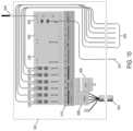
- FIG. 10shows a schematic diagram of the grid interface box (GIB) 300 according to one embodiment.
- the GIB 300is comprised of a chassis 302 , which is configured for housing a plurality of removable power modules 320 , VAR modules 330 , and at least one aggregator module 340 .
- FIGS. 11 A and 11 Bshow the GIB chassis 302 in isolation according to one embodiment.
- the GIB chassis 302includes a door 312 , which can be open and closed to access the interior portion of the chassis 302 .
- FIG. 11 Billustrates schematically a plurality of slots 314 provided in the interior portion of the chassis 302 .
- the slots 314can be dimensioned to receive and secure the removable modules 320 , 330 , 340 described herein.
- the GIB's chassis 302further includes an internal bus bar assembly 310 , to which the modules 320 , 330 , 340 can be electrically connected when inserted into the chassis' slots 314 .
- the bus bar assemblyis comprised of a two molding claim-shell with two, three, or four stamped copper bus bars with 18 mm modularity and a plurality of stabs configured for engaging the modules 320 , 330 , 340 .
- the chassisalso includes a line connection 304 for connecting the GIB 300 to an electric grid.
- the line connection wiringmay enter, for example, through the bottom of the chassis 302 through standard cable glands and knockouts.
- the GIB 300also includes a plurality of string connectors 306 , which facilitate connection of the power modules 320 within the GIB to strings of power converters 100 (as shown, for example, in FIG. 2 ).
- the string connectors 306may enter the GIB chassis 302 through dedicated cable glands with split rubber grommets.
- the line connection 304is also routed through an isolator 308 , which is configured as a disconnect switch.
- the GIBalso includes a surge arrestor block 309 (e.g., for plug in Varistor and Discharge Tube Modules).
- the GIB 300is also configured with anti-islanding functionality to disable the GIB when it detects that the electric grid has entered an islanded condition.
- the GIB's power modules 320are generally configured to unfold the deadband DC power transmitted by the power converter nodes 100 to the GIB 300 in order to convert that signal into AC power. The resulting AC power is then delivered to an electric grid via the line connection 304 .
- the power modules 320are configured to convert to AC in a 3-phase power system.
- the power modules 320may be configured to convert to AC in a single-phase or split-phase power system.
- the power modulesmay be configured to function for both 120V and 240V systems.
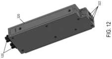
- FIG. 12illustrates a single power module 320 according to one embodiment.
- power module 320includes a pair of PWE connectors 120 at its upper end, which facilitate connection to the string connectors 306 feeding power from a string of power converter nodes 100 .
- the power module 320includes a plurality of electrical contacts 322 at its opposite end, which are configured to interface with the tabs of the GIB's bus bar assembly 310 .
- the bus bar assembly's tabswill be inserted into the electrical contacts 322 of the power module 320 , thereby electrically connecting the power module 320 with the remaining GIB components.
- the power converter nodes 100are configured to generated a deadband DC waveform 402 shaped as a rectified sinewave.
- the GIB's power modules 320are configured to invert the waveform 402 by inverting every other pulse in the waveform 402 , which are easily identifiable from the deadband periods 404 .
- the GIBis configured to monitor the grid voltage (e.g., via the line connection 304 ) in order to generate a synchronization signal transmitted to the power converter nodes 100 (e.g., via the string connectors 306 and PWE cables 200 ).
- the deadband DC waveform received and inverted by the GIBis already synchronized to the electric grid.
- the GIB 300is powered by the grid, if a particular power converter node 100 loses power, the GIB's synchronization signal will still be transmitted to the remaining operational nodes 100 , thereby ensuring synchronized AC output in phase with the utility grid AC phase.
- the power module 320may be configured to process various amounts of power.
- the power modules 320are each 40 A power modules rated at 10 kW.
- six power modules 320are provided in the slots 314 of the GIB 300 and are secured to the bus bar assembly 310 .
- the GIB 300is shown in a configuration scaled to handle 60 kW of power.
- the GIB's VAR modules 330are generally configured to adjust the amount of reactive power that is supplied to the grid.
- Many utilitiesdemand that power that is injected into the grid be power factor adjustable.
- the invertercan exert control over its “real” or “active” power (measured in kW) and its reactive power (measured in Volt Amps Reactive or VARs).
- the GIBprovides the desired about of “real” power to the grid while the VAR module 330 supplies reactive power to the grid.
- a VAR module 330is generally provided for each power module 320 inserted into the GIB 330 .
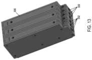
- FIG. 13illustrates a VAR module 330 according to one embodiment.
- the VAR module 330includes a plurality of electrical contacts 332 , which are configured to interface with the tabs of the GIB's bus bar assembly 310 .
- the bus bar assembly's tabswill be inserted into the electrical contacts 332 of the VAR module 330 , thereby electrically connecting the VAR module 330 with the remaining GIB components.
- the VAR moduleis a combined 3-phase module, essentially consisting of three 30 A VAR modules joined together.
- each VAR module 330 of the type shown in FIG. 13is configured to perform power factor correction for three power modules 320 in the GIB 300 .
- the GIB 300can be scaled to handle various thresholds of power by adding or removing power modules 320 and VAR modules 330 .
- the GIB 300 shown in FIGS. 2 and 10includes six power and VAR modules 320 , 330 and is therefore rated at 60 kW.
- the GIB 300 ratingcould be scaled back to 30 kW. The opposite would be true by adding additional power and VAR modules 320 , 330 .
- the modular configuration of the GIB 300which enables the power and VAR modules 320 , 330 to be easily added or removed from the GIB chassi—allows for the GIB to be easily scaled up (or down) to accommodate various solar power generation environments, including residential (e.g., 10 kW), commercial (e.g., 30-60 kW), and utility scale (e.g., 120 kW+) applications.
- residentiale.g. 10 kW
- commerciale.g., 30-60 kW
- utility scalee.g. 120 kW+
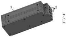
- the GIB's aggregator module 340is configured to control the operation of the GIB 300 and function as a communications gateway between the remaining components of the solar power generation system (e.g., power converter nodes 100 ) and remote devices (e.g., computers configured for interoperability with the GIB 300 ).
- the aggregator module 340includes at least one dedicated processor and associated memory storage for running software and applications related to the GIB's functionality.
- the aggregator module 340is configured to send and receive data from the power converter nodes 100 and power modules 320 via the bus bar assembly 310 and the various PWE cables 200 connecting the nodes 100 to the GIB 300 .
- the aggregator module 340includes a Wi-Fi antenna 346 , which is configured to provide communication with the aggregator module 340 over a wireless internet network, and an Ethernet uplink 344 , which is configured to provide communication with the aggregator module 340 over a dedicated network.
- FIG. 14illustrates an aggregator module 340 according to one embodiment.
- the aggregator module 340includes a plurality of electrical contacts 342 , which are configured to interface with the tabs of the GIB's bus bar assembly 310 .
- the bus bar assembly's tabswill be inserted into the electrical contacts 342 of the aggregator module 340 , thereby electrically connecting the aggregator module 340 with the remaining GIB components.
- the aggregator module 340is configured to function as a bridge for internal and external network connectivity, handle supervisory control and data acquisition operations from the grid, and collect and perform edge mining on all sensor data (e.g., collected from the power converter nodes 100 ), and to host installer and maintainer applications.
- the aggregatoralso provides system wide control functions to shut down or scale back output when external commands (e.g., from the utility) are received.
- the GIB 300can be configured to convert to AC in a 3-phase power system or single (or split-phase) power system at 120V or 240V.
- FIG. 15shows the GIB 300 in a 3-phase WYE configuration
- FIG. 16shows the GIB 300 in a 3-phase delta configuration
- FIG. 17shows the GIB 300 in a single-phase configuration.
Landscapes
- Engineering & Computer Science (AREA)
- Power Engineering (AREA)
- Life Sciences & Earth Sciences (AREA)
- Sustainable Development (AREA)
- Sustainable Energy (AREA)
- Inverter Devices (AREA)
- Supply And Distribution Of Alternating Current (AREA)
Abstract
Description
Claims (15)
Priority Applications (1)
| Application Number | Priority Date | Filing Date | Title |
|---|---|---|---|
| US17/589,097US12184159B2 (en) | 2017-08-03 | 2022-01-31 | Solar power generation system |
Applications Claiming Priority (4)
| Application Number | Priority Date | Filing Date | Title |
|---|---|---|---|
| US201762540951P | 2017-08-03 | 2017-08-03 | |
| US201762567488P | 2017-10-03 | 2017-10-03 | |
| US16/054,625US11251621B1 (en) | 2017-08-03 | 2018-08-03 | Solar power generation system |
| US17/589,097US12184159B2 (en) | 2017-08-03 | 2022-01-31 | Solar power generation system |
Related Parent Applications (1)
| Application Number | Title | Priority Date | Filing Date |
|---|---|---|---|
| US16/054,625ContinuationUS11251621B1 (en) | 2017-08-03 | 2018-08-03 | Solar power generation system |
Publications (2)
| Publication Number | Publication Date |
|---|---|
| US20220231514A1 US20220231514A1 (en) | 2022-07-21 |
| US12184159B2true US12184159B2 (en) | 2024-12-31 |
Family
ID=80249660
Family Applications (2)
| Application Number | Title | Priority Date | Filing Date |
|---|---|---|---|
| US16/054,625Active2039-07-17US11251621B1 (en) | 2017-08-03 | 2018-08-03 | Solar power generation system |
| US17/589,097ActiveUS12184159B2 (en) | 2017-08-03 | 2022-01-31 | Solar power generation system |
Family Applications Before (1)
| Application Number | Title | Priority Date | Filing Date |
|---|---|---|---|
| US16/054,625Active2039-07-17US11251621B1 (en) | 2017-08-03 | 2018-08-03 | Solar power generation system |
Country Status (1)
| Country | Link |
|---|---|
| US (2) | US11251621B1 (en) |
Cited By (1)
| Publication number | Priority date | Publication date | Assignee | Title |
|---|---|---|---|---|
| US20220080845A1 (en)* | 2019-05-27 | 2022-03-17 | Abb Schweiz Ag | Electric vehicle supply equipment for charging an electrical vehicle |
Families Citing this family (3)
| Publication number | Priority date | Publication date | Assignee | Title |
|---|---|---|---|---|
| US11251621B1 (en) | 2017-08-03 | 2022-02-15 | Southwire Company, Llc | Solar power generation system |
| US11438988B1 (en) | 2017-08-11 | 2022-09-06 | Southwire Company, Llc | DC power management system |
| US12382520B2 (en)* | 2022-11-11 | 2025-08-05 | Tigo Energy, Inc. | Solar panel transmitter pairing process |
Citations (114)
| Publication number | Priority date | Publication date | Assignee | Title |
|---|---|---|---|---|
| JPH10174452A (en) | 1996-12-10 | 1998-06-26 | Omron Corp | Power conversion device, inverter and photovoltaic power generation system |
| US6111767A (en) | 1998-06-22 | 2000-08-29 | Heliotronics, Inc. | Inverter integrated instrumentation having a current-voltage curve tracer |
| JP2001238466A (en) | 2000-02-28 | 2001-08-31 | Matsushita Electric Ind Co Ltd | Grid-connected inverter device |
| US6429546B1 (en) | 1998-11-20 | 2002-08-06 | Georgia Tech Research Corporation | Systems and methods for preventing islanding of grid-connected electrical power systems |
| WO2003077398A2 (en) | 2002-03-08 | 2003-09-18 | Aloys Wobben | Separate network and method for operating a separate network |
| US20050080520A1 (en) | 2003-09-22 | 2005-04-14 | Robert Kline | Waste recovery and material handling process to replace the traditional trash transfer station and landfil by extracting reusable material and energy from joined refuse streams to include; office waste, dry waste, wet garbage and the special hazardous material handling of biological, chemical, and nuclear waste |
| US20050128751A1 (en) | 2003-05-05 | 2005-06-16 | Color Kinetics, Incorporated | Lighting methods and systems |
| US20060002110A1 (en) | 2004-03-15 | 2006-01-05 | Color Kinetics Incorporated | Methods and systems for providing lighting systems |
| WO2006005125A1 (en) | 2004-07-13 | 2006-01-19 | Central Queensland University | A device for distributed maximum power tracking for solar arrays |
| US20070247823A1 (en) | 2006-04-22 | 2007-10-25 | Sma Technologie Ag | Power inverter |
| US20080236648A1 (en) | 2007-03-30 | 2008-10-02 | Klein David L | Localized power point optimizer for solar cell installations |
| US20080285317A1 (en) | 2007-05-17 | 2008-11-20 | Larankelo, Inc. | Photovoltaic module-mounted ac inverter |
| US20090275242A1 (en) | 2008-05-02 | 2009-11-05 | Cooper Technologies Company | Combined power and data transmission cable connector systems |
| US20100066260A1 (en) | 2008-09-05 | 2010-03-18 | Lutron Electronics Co., Inc. | Hybrid light source |
| US20100071742A1 (en)* | 2008-09-19 | 2010-03-25 | General Electric Company | Quasi-AC, photovoltaic module for unfolder photovoltaic inverter |
| US20100134959A1 (en) | 2008-11-11 | 2010-06-03 | Fife John M | Solar power inverters, including temperature-controlled solar power inverters, and associated systems and methods |
| US20100145532A1 (en)* | 2008-11-04 | 2010-06-10 | Daniel Constantine Gregory | Distributed hybrid renewable energy power plant and methods, systems, and comptuer readable media for controlling a distributed hybrid renewable energy power plant |
| US20100141158A1 (en) | 2008-09-05 | 2010-06-10 | Newman Jr Robert C | Hybrid light source |
| US20100263704A1 (en) | 2009-04-16 | 2010-10-21 | Enphase Energy, Inc. | Apparatus for coupling power generated by a photovoltaic module to an output |
| US20100289337A1 (en) | 2009-05-13 | 2010-11-18 | Solar Semiconductor, Inc. | Methods and apparatuses for photovoltaic power management |
| US20100307479A1 (en) | 2009-06-03 | 2010-12-09 | Ken Hyun Park | Solar Panel Tracking and Mounting System |
| US20110056533A1 (en) | 2009-09-10 | 2011-03-10 | Kan-Sheng Kuan | Series solar system with current-matching function |
| US20110061705A1 (en) | 2009-09-11 | 2011-03-17 | Miasole | Rotatable junction box for a solar module |
| US20110080105A1 (en) | 2009-10-05 | 2011-04-07 | Mayer Thomas J | Variable light control system and method using momentary circuit interrupt |
| US20110090089A1 (en) | 2009-10-15 | 2011-04-21 | Yuhao Luo | Method and apparatus for detecting a fault in a solar cell panel and an inverter |
| US20110103117A1 (en) | 2009-10-30 | 2011-05-05 | Sanyo Electric Co., Ltd. | Grid interconnection inverter and grid interconnection device |
| US20110121744A1 (en) | 2009-11-20 | 2011-05-26 | Lutron Electronics Co., Inc. | Controllable-load circuit for use with a load control device |
| US20110202181A1 (en) | 2010-02-12 | 2011-08-18 | Enphase Energy, Inc. | Method and apparatus for smart climate control |
| US20110197945A1 (en)* | 2010-02-16 | 2011-08-18 | Betronic Solutions B.V. | Electrically parallel connection of photovoltaic modules in a string to provide a dc voltage to a dc voltage bus |
| US20110210611A1 (en) | 2008-10-10 | 2011-09-01 | Ampt, Llc | Novel Solar Power Circuits |
| US20110225904A1 (en) | 2010-03-19 | 2011-09-22 | Sudhir Railkar | Slate Style Roofing System with Integrated Solar Panels |
| US20110248640A1 (en) | 2008-09-05 | 2011-10-13 | Petrus Johannes Maria Welten | Led based lighting application |
| US20110273016A1 (en) | 2007-12-04 | 2011-11-10 | Solaredge Technologies Ltd. | Distributed power harvesting systems using dc power sources |
| US20110273015A1 (en) | 2006-12-06 | 2011-11-10 | Solaredge Technologies Ltd. | Distributed power harvesting systems using dc power sources |
| US20120019074A1 (en) | 2011-09-29 | 2012-01-26 | Sunlight Photonics Inc. | Methods and apparatus for high-frequency electrical power collection and transfer |
| US8106537B2 (en) | 2008-07-01 | 2012-01-31 | Satcon Technology Corporation | Photovoltaic DC/DC micro-converter |
| GB2483317A (en) | 2011-01-12 | 2012-03-07 | Solaredge Technologies Ltd | Photovoltaic power generation system |
| US8134820B1 (en) | 2007-09-10 | 2012-03-13 | Technology Reasearch Corporation | Contactor control circuit |
| US20120080944A1 (en) | 2006-03-28 | 2012-04-05 | Wireless Environment, Llc. | Grid Shifting System for a Lighting Circuit |
| US20120081934A1 (en) | 2011-11-01 | 2012-04-05 | Paul Garrity | Photovoltaic power conditioning units |
| US20120084027A1 (en) | 2010-10-05 | 2012-04-05 | Also Energy, Inc. | System and method for monitoring performance of a photovoltaic array |
| US20120089260A1 (en) | 2010-10-11 | 2012-04-12 | Solarbridge Technologies, Inc. | System and method for establishing communication with an array of inverters |
| US20120138123A1 (en) | 2009-08-14 | 2012-06-07 | Newdoll Enterprises Llc | Enhanced solar panels, liquid delivery systems and associated processes for solar energy systems |
| US8207637B2 (en) | 2009-10-09 | 2012-06-26 | Solarbridge Technologies, Inc. | System and apparatus for interconnecting an array of power generating assemblies |
| US20120175955A1 (en) | 2011-01-12 | 2012-07-12 | The Boeing Company | Smart microgrid reconfigurable ac interface |
| US8257106B2 (en) | 2010-01-25 | 2012-09-04 | Enphase Energy, Inc. | Method and apparatus for interconnecting distributed power sources |
| CN202444440U (en) | 2012-02-27 | 2012-09-19 | 无锡联动太阳能科技有限公司 | Bridgeless inverter circuit and solar bridgeless inverter |
| US8278845B1 (en) | 2011-07-26 | 2012-10-02 | Hunter Industries, Inc. | Systems and methods for providing power and data to lighting devices |
| US20120248863A1 (en) | 2006-12-06 | 2012-10-04 | Solaredge Technologies Ltd. | Safety Mechanisms, Wake Up and Shutdown Methods in Distributed Power Installations |
| US20120249150A1 (en) | 2011-03-31 | 2012-10-04 | Osram Sylvania Inc. | Switch status detection circuit for multiple light level lighting systems |
| US20120250372A1 (en) | 2011-03-29 | 2012-10-04 | Sony Corporation | Grid tied inverter, system and method |
| CN202550576U (en) | 2010-11-23 | 2012-11-21 | 雅达电子国际有限公司 | Power conversion system for photovoltaic power supply and power system |
| US20120310427A1 (en) | 2011-05-31 | 2012-12-06 | Williams B Jeffery | Automatic Monitoring and Adjustment of a Solar Panel Array |
| WO2012170726A2 (en) | 2011-06-07 | 2012-12-13 | Transform Solar Pty Ltd. | Solar panel systems having solar panels arranged in parallel, and associated methods |
| US20120313443A1 (en) | 2011-06-10 | 2012-12-13 | Cyboenergy, Inc. | Smart and scalable off-grid mini-inverters |
| US20130002031A1 (en) | 2011-06-30 | 2013-01-03 | Cyboenergy, Inc. | Enclosure and Message System of Smart and Scalable Power Inverters |
| US20130021006A1 (en) | 2011-07-18 | 2013-01-24 | Enphase Energy, Inc. | Method and apparatus for multi-phase power transfer |
| US20130049674A1 (en) | 2011-08-24 | 2013-02-28 | Qualcomm Incorporated | Integrated photo voltaic solar plant and electric vehicle charging station and method of operation |
| US20130049610A1 (en) | 2011-08-31 | 2013-02-28 | Chia-Teh Chen | Two-level led security light with motion sensor |
| US8410950B2 (en) | 2009-08-17 | 2013-04-02 | Paceco Corp. | Photovoltaic panel monitoring apparatus |
| US20130113291A1 (en) | 2006-03-28 | 2013-05-09 | Wireless Environment, Llc | Distributed energy managment using grid-shifting devices |
| US20130134891A1 (en) | 2011-07-26 | 2013-05-30 | Hunter Industries, Inc. | Systems and methods for providing power and data to lighting devices |
| WO2013107782A2 (en) | 2012-01-17 | 2013-07-25 | Infineon Technologies Austria Ag | Power converter circuit, power supply system and method |
| US20130225005A1 (en) | 2010-01-25 | 2013-08-29 | Enphase Energy, Inc. | Method and apparatus for interconnecting distributed power sources |
| CN103312021A (en) | 2012-03-14 | 2013-09-18 | 株式会社电装 | Solar power conditioner |
| US20130241535A1 (en) | 2010-11-10 | 2013-09-19 | Sma Solar Technology Ag | Method for Verifying an Electrical Connection Between a Generator and an Inverter |
| US20130250634A1 (en)* | 2006-03-23 | 2013-09-26 | Enphase Energy, Inc. | Method and apparatus for power conversion |
| US8581441B2 (en) | 2007-05-17 | 2013-11-12 | Enphase Energy, Inc. | Distributed inverter and intelligent gateway |
| US20130307342A1 (en) | 2011-11-07 | 2013-11-21 | Fairchild Semiconductor Corporation | Photovoltaic System Power Optimization |
| US20130346054A1 (en) | 2012-06-26 | 2013-12-26 | Asim Mumtaz | System, method and apparatus for generating layout of devices in solar installations |
| US8626616B2 (en) | 2010-04-01 | 2014-01-07 | Enphase Energy, Inc. | Method and apparatus for managing installation information |
| US20140077609A1 (en) | 2012-09-19 | 2014-03-20 | Enphase Energy, Inc. | Serially connected micro-inverter system with trunk and drop cabling |
| US20140102755A1 (en) | 2012-10-17 | 2014-04-17 | Commscope, Inc. Of North Carolina | Communications Cables Having Electrically Insulative but Thermally Conductive Cable Jackets |
| US20140117769A1 (en) | 2012-10-25 | 2014-05-01 | SunEdison Microinverter Products LLC | Master slave architecture for distributed dc to ac power conversion |
| US20140191583A1 (en) | 2013-01-04 | 2014-07-10 | Enecsys Limited | Power balancing in a multi-phase system |
| US8824178B1 (en) | 2009-12-31 | 2014-09-02 | Solarbridge Technologies, Inc. | Parallel power converter topology |
| EP2773036A1 (en) | 2013-02-27 | 2014-09-03 | Optistring Technologies AB | Method for DC-AC conversion |
| US20140266289A1 (en) | 2013-03-15 | 2014-09-18 | Technology Research Corporation | Interface for renewable energy system |
| US20140265585A1 (en) | 2013-03-15 | 2014-09-18 | Technology Research Corporation | Interface for renewable energy system |
| US20140265550A1 (en) | 2013-03-14 | 2014-09-18 | Raytheon Bbn Technologies Corp. | Redundantly powered and daisy chained power over ethernet |
| CN104158394A (en) | 2014-07-08 | 2014-11-19 | 安徽金峰新能源股份有限公司 | Auto-starting control method for photovoltaic inverter |
| US20140361695A1 (en) | 2011-10-04 | 2014-12-11 | Citizen Electronics Co., Ltd. | Led lighting device |
| US20140376270A1 (en)* | 2013-06-20 | 2014-12-25 | Sunedison Llc | Power converters including llc converters and methods of controlling the same |
| US20150002040A1 (en) | 2012-02-01 | 2015-01-01 | Koninklijke Philips N.V. | Driver device and driving method for driving a load, in particular a LED unit comprising one or more LEDs |
| WO2015015112A1 (en) | 2013-07-30 | 2015-02-05 | Commissariat A L'energie Atomique Et Aux Energies Alternatives | Photovoltaic plant linked to a high-voltage electrical network |
| TW201519555A (en) | 2013-11-14 | 2015-05-16 | Au Optronics Corp | Photovoltaic module and control method thereof |
| US20150216002A1 (en) | 2014-01-28 | 2015-07-30 | Cirrus Logic, Inc. | Low-cost low-power lighting system and lamp assembly |
| US20150237700A1 (en) | 2011-07-26 | 2015-08-20 | Hunter Industries, Inc. | Systems and methods to control color and brightness of lighting devices |
| US20150244250A1 (en) | 2012-10-03 | 2015-08-27 | Belenos Clean Power Holding Ag | Regulation of an electronic voltage adapter module |
| US9165275B2 (en) | 2009-07-14 | 2015-10-20 | Emphase Energy, Inc. | Method and apparatus for identifying redeployed distributed generator components |
| US9270201B1 (en) | 2012-10-25 | 2016-02-23 | mPower Solar Inc. | Solar inverter |
| US20160066386A1 (en) | 2009-01-13 | 2016-03-03 | Terralux, Inc. | Method and device for remote sensing and control of led lights |
| US20160072396A1 (en) | 2014-09-08 | 2016-03-10 | Infineon Technologies Austria Ag | Multi-cell power conversion method and multi-cell power converter |
| US20160094034A1 (en)* | 2014-04-24 | 2016-03-31 | Varentec, Inc. | Controlling demand and energy through photovoltaic inverters delivering vars |
| US20160226252A1 (en) | 2015-02-02 | 2016-08-04 | Technology Research, Llc | Interface for renewable energy system |
| US20160270174A1 (en) | 2013-11-07 | 2016-09-15 | Isotera Ltd | Power Distribution |
| US20160270193A1 (en) | 2013-09-23 | 2016-09-15 | Philips Lighting Holding B.V. | A lighting device and a method of protecting a lighting device |
| US20160299555A1 (en) | 2015-04-07 | 2016-10-13 | Liteideas, Llc | Device and Method for Encoding a Signal on Alternating Current Lines |
| US20160360594A1 (en) | 2013-10-10 | 2016-12-08 | Digital Lumens, Inc. | Methods, systems, and apparatus for intelligent lighting |
| US20170019960A1 (en) | 2015-07-14 | 2017-01-19 | The Hong Kong Polytechnic University | Multi-string led driver with current balancing |
| US20170027029A1 (en) | 2011-03-17 | 2017-01-26 | Shanghai Sim-Bcd Semiconductor Manufacturing Co., Ltd. | Power supply for led lamp with triac dimmer |
| US20170179876A1 (en) | 2015-12-18 | 2017-06-22 | Southwire Company, Llc | Cable integrated solar inverter |
| US20170223807A1 (en) | 2006-03-28 | 2017-08-03 | Wireless Environment, Llc. | Cloud connected lighting system |
| US20170231058A1 (en) | 2014-08-04 | 2017-08-10 | Innosys, Inc. | Lighting Systems |
| US20170238401A1 (en) | 2014-01-25 | 2017-08-17 | Innosys, Inc. | Solid State Lighting Systems |
| US9750102B1 (en) | 2016-04-06 | 2017-08-29 | Power Integrations, Inc. | Switch current control to shape input current |
| US20170332462A1 (en) | 2016-05-13 | 2017-11-16 | Lumastream Canada Ulc | Network connected low voltage lighting system |
| US20180211509A1 (en) | 2017-01-26 | 2018-07-26 | Elements of Genius, Inc. | Wearable interactive notification device and interactive notification system |
| US20190029099A1 (en) | 2017-07-21 | 2019-01-24 | General Electric Company | Led lamp |
| US20190280895A1 (en)* | 2016-07-18 | 2019-09-12 | Commscope Technologies Llc | Systems and methods for high capacity power delivery to remote nodes |
| US10523117B2 (en) | 2016-11-07 | 2019-12-31 | Southwire Company, Llc | Dead band direct current converter |
| US11251621B1 (en) | 2017-08-03 | 2022-02-15 | Southwire Company, Llc | Solar power generation system |
| US11438988B1 (en) | 2017-08-11 | 2022-09-06 | Southwire Company, Llc | DC power management system |
| US11438980B2 (en) | 2018-09-04 | 2022-09-06 | Lutron Technology Company Llc | Communicating with and controlling load control systems |
- 2018
- 2018-08-03USUS16/054,625patent/US11251621B1/enactiveActive
- 2022
- 2022-01-31USUS17/589,097patent/US12184159B2/enactiveActive
Patent Citations (126)
| Publication number | Priority date | Publication date | Assignee | Title |
|---|---|---|---|---|
| JPH10174452A (en) | 1996-12-10 | 1998-06-26 | Omron Corp | Power conversion device, inverter and photovoltaic power generation system |
| US6111767A (en) | 1998-06-22 | 2000-08-29 | Heliotronics, Inc. | Inverter integrated instrumentation having a current-voltage curve tracer |
| US6429546B1 (en) | 1998-11-20 | 2002-08-06 | Georgia Tech Research Corporation | Systems and methods for preventing islanding of grid-connected electrical power systems |
| JP2001238466A (en) | 2000-02-28 | 2001-08-31 | Matsushita Electric Ind Co Ltd | Grid-connected inverter device |
| WO2003077398A2 (en) | 2002-03-08 | 2003-09-18 | Aloys Wobben | Separate network and method for operating a separate network |
| US20050200133A1 (en)* | 2002-03-08 | 2005-09-15 | Aloys Wobben | Separate network and method for operating a separate network |
| US20050128751A1 (en) | 2003-05-05 | 2005-06-16 | Color Kinetics, Incorporated | Lighting methods and systems |
| US20050080520A1 (en) | 2003-09-22 | 2005-04-14 | Robert Kline | Waste recovery and material handling process to replace the traditional trash transfer station and landfil by extracting reusable material and energy from joined refuse streams to include; office waste, dry waste, wet garbage and the special hazardous material handling of biological, chemical, and nuclear waste |
| US20060002110A1 (en) | 2004-03-15 | 2006-01-05 | Color Kinetics Incorporated | Methods and systems for providing lighting systems |
| WO2006005125A1 (en) | 2004-07-13 | 2006-01-19 | Central Queensland University | A device for distributed maximum power tracking for solar arrays |
| US20130250634A1 (en)* | 2006-03-23 | 2013-09-26 | Enphase Energy, Inc. | Method and apparatus for power conversion |
| US20130113291A1 (en) | 2006-03-28 | 2013-05-09 | Wireless Environment, Llc | Distributed energy managment using grid-shifting devices |
| US20120080944A1 (en) | 2006-03-28 | 2012-04-05 | Wireless Environment, Llc. | Grid Shifting System for a Lighting Circuit |
| US20170223807A1 (en) | 2006-03-28 | 2017-08-03 | Wireless Environment, Llc. | Cloud connected lighting system |
| US20070247823A1 (en) | 2006-04-22 | 2007-10-25 | Sma Technologie Ag | Power inverter |
| US20120248863A1 (en) | 2006-12-06 | 2012-10-04 | Solaredge Technologies Ltd. | Safety Mechanisms, Wake Up and Shutdown Methods in Distributed Power Installations |
| US20110273015A1 (en) | 2006-12-06 | 2011-11-10 | Solaredge Technologies Ltd. | Distributed power harvesting systems using dc power sources |
| US20080236648A1 (en) | 2007-03-30 | 2008-10-02 | Klein David L | Localized power point optimizer for solar cell installations |
| US20130012061A1 (en) | 2007-05-17 | 2013-01-10 | Enphase Energy, Inc. | Photovoltaic ac inverter mount and interconnect |
| US8581441B2 (en) | 2007-05-17 | 2013-11-12 | Enphase Energy, Inc. | Distributed inverter and intelligent gateway |
| US20080285317A1 (en) | 2007-05-17 | 2008-11-20 | Larankelo, Inc. | Photovoltaic module-mounted ac inverter |
| US8134820B1 (en) | 2007-09-10 | 2012-03-13 | Technology Reasearch Corporation | Contactor control circuit |
| US20110273016A1 (en) | 2007-12-04 | 2011-11-10 | Solaredge Technologies Ltd. | Distributed power harvesting systems using dc power sources |
| US20090275242A1 (en) | 2008-05-02 | 2009-11-05 | Cooper Technologies Company | Combined power and data transmission cable connector systems |
| US8106537B2 (en) | 2008-07-01 | 2012-01-31 | Satcon Technology Corporation | Photovoltaic DC/DC micro-converter |
| US20100141158A1 (en) | 2008-09-05 | 2010-06-10 | Newman Jr Robert C | Hybrid light source |
| US20110248640A1 (en) | 2008-09-05 | 2011-10-13 | Petrus Johannes Maria Welten | Led based lighting application |
| US20100066260A1 (en) | 2008-09-05 | 2010-03-18 | Lutron Electronics Co., Inc. | Hybrid light source |
| US20100071742A1 (en)* | 2008-09-19 | 2010-03-25 | General Electric Company | Quasi-AC, photovoltaic module for unfolder photovoltaic inverter |
| US20110210611A1 (en) | 2008-10-10 | 2011-09-01 | Ampt, Llc | Novel Solar Power Circuits |
| US20100145532A1 (en)* | 2008-11-04 | 2010-06-10 | Daniel Constantine Gregory | Distributed hybrid renewable energy power plant and methods, systems, and comptuer readable media for controlling a distributed hybrid renewable energy power plant |
| US20100134959A1 (en) | 2008-11-11 | 2010-06-03 | Fife John M | Solar power inverters, including temperature-controlled solar power inverters, and associated systems and methods |
| US20160066386A1 (en) | 2009-01-13 | 2016-03-03 | Terralux, Inc. | Method and device for remote sensing and control of led lights |
| US8435056B2 (en) | 2009-04-16 | 2013-05-07 | Enphase Energy, Inc. | Apparatus for coupling power generated by a photovoltaic module to an output |
| US20100263704A1 (en) | 2009-04-16 | 2010-10-21 | Enphase Energy, Inc. | Apparatus for coupling power generated by a photovoltaic module to an output |
| US20100289337A1 (en) | 2009-05-13 | 2010-11-18 | Solar Semiconductor, Inc. | Methods and apparatuses for photovoltaic power management |
| US20100307479A1 (en) | 2009-06-03 | 2010-12-09 | Ken Hyun Park | Solar Panel Tracking and Mounting System |
| US9165275B2 (en) | 2009-07-14 | 2015-10-20 | Emphase Energy, Inc. | Method and apparatus for identifying redeployed distributed generator components |
| US20120138123A1 (en) | 2009-08-14 | 2012-06-07 | Newdoll Enterprises Llc | Enhanced solar panels, liquid delivery systems and associated processes for solar energy systems |
| US8410950B2 (en) | 2009-08-17 | 2013-04-02 | Paceco Corp. | Photovoltaic panel monitoring apparatus |
| US20110056533A1 (en) | 2009-09-10 | 2011-03-10 | Kan-Sheng Kuan | Series solar system with current-matching function |
| US20110061705A1 (en) | 2009-09-11 | 2011-03-17 | Miasole | Rotatable junction box for a solar module |
| US20110080105A1 (en) | 2009-10-05 | 2011-04-07 | Mayer Thomas J | Variable light control system and method using momentary circuit interrupt |
| US8207637B2 (en) | 2009-10-09 | 2012-06-26 | Solarbridge Technologies, Inc. | System and apparatus for interconnecting an array of power generating assemblies |
| US20110090089A1 (en) | 2009-10-15 | 2011-04-21 | Yuhao Luo | Method and apparatus for detecting a fault in a solar cell panel and an inverter |
| US20110103117A1 (en) | 2009-10-30 | 2011-05-05 | Sanyo Electric Co., Ltd. | Grid interconnection inverter and grid interconnection device |
| US20110121744A1 (en) | 2009-11-20 | 2011-05-26 | Lutron Electronics Co., Inc. | Controllable-load circuit for use with a load control device |
| US8824178B1 (en) | 2009-12-31 | 2014-09-02 | Solarbridge Technologies, Inc. | Parallel power converter topology |
| US20130225005A1 (en) | 2010-01-25 | 2013-08-29 | Enphase Energy, Inc. | Method and apparatus for interconnecting distributed power sources |
| US8257106B2 (en) | 2010-01-25 | 2012-09-04 | Enphase Energy, Inc. | Method and apparatus for interconnecting distributed power sources |
| US20110202181A1 (en) | 2010-02-12 | 2011-08-18 | Enphase Energy, Inc. | Method and apparatus for smart climate control |
| US20110197945A1 (en)* | 2010-02-16 | 2011-08-18 | Betronic Solutions B.V. | Electrically parallel connection of photovoltaic modules in a string to provide a dc voltage to a dc voltage bus |
| US20110225904A1 (en) | 2010-03-19 | 2011-09-22 | Sudhir Railkar | Slate Style Roofing System with Integrated Solar Panels |
| US8626616B2 (en) | 2010-04-01 | 2014-01-07 | Enphase Energy, Inc. | Method and apparatus for managing installation information |
| US20120084027A1 (en) | 2010-10-05 | 2012-04-05 | Also Energy, Inc. | System and method for monitoring performance of a photovoltaic array |
| US20120089260A1 (en) | 2010-10-11 | 2012-04-12 | Solarbridge Technologies, Inc. | System and method for establishing communication with an array of inverters |
| US20130241535A1 (en) | 2010-11-10 | 2013-09-19 | Sma Solar Technology Ag | Method for Verifying an Electrical Connection Between a Generator and an Inverter |
| CN202550576U (en) | 2010-11-23 | 2012-11-21 | 雅达电子国际有限公司 | Power conversion system for photovoltaic power supply and power system |
| US20120175955A1 (en) | 2011-01-12 | 2012-07-12 | The Boeing Company | Smart microgrid reconfigurable ac interface |
| US20120175964A1 (en) | 2011-01-12 | 2012-07-12 | Solaredge Technologies Ltd. | Serially connected inverters |
| GB2483317A (en) | 2011-01-12 | 2012-03-07 | Solaredge Technologies Ltd | Photovoltaic power generation system |
| US20170027029A1 (en) | 2011-03-17 | 2017-01-26 | Shanghai Sim-Bcd Semiconductor Manufacturing Co., Ltd. | Power supply for led lamp with triac dimmer |
| US20120250372A1 (en) | 2011-03-29 | 2012-10-04 | Sony Corporation | Grid tied inverter, system and method |
| US20120249150A1 (en) | 2011-03-31 | 2012-10-04 | Osram Sylvania Inc. | Switch status detection circuit for multiple light level lighting systems |
| US20120310427A1 (en) | 2011-05-31 | 2012-12-06 | Williams B Jeffery | Automatic Monitoring and Adjustment of a Solar Panel Array |
| WO2012170726A2 (en) | 2011-06-07 | 2012-12-13 | Transform Solar Pty Ltd. | Solar panel systems having solar panels arranged in parallel, and associated methods |
| US20120313443A1 (en) | 2011-06-10 | 2012-12-13 | Cyboenergy, Inc. | Smart and scalable off-grid mini-inverters |
| US20130002031A1 (en) | 2011-06-30 | 2013-01-03 | Cyboenergy, Inc. | Enclosure and Message System of Smart and Scalable Power Inverters |
| US20130021006A1 (en) | 2011-07-18 | 2013-01-24 | Enphase Energy, Inc. | Method and apparatus for multi-phase power transfer |
| US20130134891A1 (en) | 2011-07-26 | 2013-05-30 | Hunter Industries, Inc. | Systems and methods for providing power and data to lighting devices |
| US20150237700A1 (en) | 2011-07-26 | 2015-08-20 | Hunter Industries, Inc. | Systems and methods to control color and brightness of lighting devices |
| US8278845B1 (en) | 2011-07-26 | 2012-10-02 | Hunter Industries, Inc. | Systems and methods for providing power and data to lighting devices |
| US20130049674A1 (en) | 2011-08-24 | 2013-02-28 | Qualcomm Incorporated | Integrated photo voltaic solar plant and electric vehicle charging station and method of operation |
| US20130049610A1 (en) | 2011-08-31 | 2013-02-28 | Chia-Teh Chen | Two-level led security light with motion sensor |
| US20120019074A1 (en) | 2011-09-29 | 2012-01-26 | Sunlight Photonics Inc. | Methods and apparatus for high-frequency electrical power collection and transfer |
| US20140361695A1 (en) | 2011-10-04 | 2014-12-11 | Citizen Electronics Co., Ltd. | Led lighting device |
| US20120081934A1 (en) | 2011-11-01 | 2012-04-05 | Paul Garrity | Photovoltaic power conditioning units |
| US8472220B2 (en) | 2011-11-01 | 2013-06-25 | Enecsys Limited | Photovoltaic power conditioning units |
| US20130307342A1 (en) | 2011-11-07 | 2013-11-21 | Fairchild Semiconductor Corporation | Photovoltaic System Power Optimization |
| WO2013107782A2 (en) | 2012-01-17 | 2013-07-25 | Infineon Technologies Austria Ag | Power converter circuit, power supply system and method |
| US20150002040A1 (en) | 2012-02-01 | 2015-01-01 | Koninklijke Philips N.V. | Driver device and driving method for driving a load, in particular a LED unit comprising one or more LEDs |
| CN202444440U (en) | 2012-02-27 | 2012-09-19 | 无锡联动太阳能科技有限公司 | Bridgeless inverter circuit and solar bridgeless inverter |
| US20130242628A1 (en) | 2012-03-14 | 2013-09-19 | Denso Corporation | Solar power conditioner |
| CN103312021A (en) | 2012-03-14 | 2013-09-18 | 株式会社电装 | Solar power conditioner |
| US20130346054A1 (en) | 2012-06-26 | 2013-12-26 | Asim Mumtaz | System, method and apparatus for generating layout of devices in solar installations |
| US20140077609A1 (en) | 2012-09-19 | 2014-03-20 | Enphase Energy, Inc. | Serially connected micro-inverter system with trunk and drop cabling |
| US20150244250A1 (en) | 2012-10-03 | 2015-08-27 | Belenos Clean Power Holding Ag | Regulation of an electronic voltage adapter module |
| US20140102755A1 (en) | 2012-10-17 | 2014-04-17 | Commscope, Inc. Of North Carolina | Communications Cables Having Electrically Insulative but Thermally Conductive Cable Jackets |
| US20140117769A1 (en) | 2012-10-25 | 2014-05-01 | SunEdison Microinverter Products LLC | Master slave architecture for distributed dc to ac power conversion |
| US9270201B1 (en) | 2012-10-25 | 2016-02-23 | mPower Solar Inc. | Solar inverter |
| US20140191583A1 (en) | 2013-01-04 | 2014-07-10 | Enecsys Limited | Power balancing in a multi-phase system |
| EP2773036A1 (en) | 2013-02-27 | 2014-09-03 | Optistring Technologies AB | Method for DC-AC conversion |
| US20140265550A1 (en) | 2013-03-14 | 2014-09-18 | Raytheon Bbn Technologies Corp. | Redundantly powered and daisy chained power over ethernet |
| US20140266289A1 (en) | 2013-03-15 | 2014-09-18 | Technology Research Corporation | Interface for renewable energy system |
| EP2973976B1 (en) | 2013-03-15 | 2019-05-01 | Technology Research, LLC | Interface for renewable energy system |
| US20140265585A1 (en) | 2013-03-15 | 2014-09-18 | Technology Research Corporation | Interface for renewable energy system |
| WO2014152765A2 (en) | 2013-03-15 | 2014-09-25 | Technology Research Corporation | Interface for renewable energy system |
| CA2906590A1 (en) | 2013-03-15 | 2014-09-25 | Technology Research, Llc | Interface for renewable energy system |
| US20140376270A1 (en)* | 2013-06-20 | 2014-12-25 | Sunedison Llc | Power converters including llc converters and methods of controlling the same |
| US20160172858A1 (en) | 2013-07-30 | 2016-06-16 | Commissariat A L'energie Atomique Et Aux Energies Alternatives | Photovoltaic plant linked to a high-voltage electrical network |
| WO2015015112A1 (en) | 2013-07-30 | 2015-02-05 | Commissariat A L'energie Atomique Et Aux Energies Alternatives | Photovoltaic plant linked to a high-voltage electrical network |
| US20160270193A1 (en) | 2013-09-23 | 2016-09-15 | Philips Lighting Holding B.V. | A lighting device and a method of protecting a lighting device |
| US20160360594A1 (en) | 2013-10-10 | 2016-12-08 | Digital Lumens, Inc. | Methods, systems, and apparatus for intelligent lighting |
| US20160270174A1 (en) | 2013-11-07 | 2016-09-15 | Isotera Ltd | Power Distribution |
| TW201519555A (en) | 2013-11-14 | 2015-05-16 | Au Optronics Corp | Photovoltaic module and control method thereof |
| US20170238401A1 (en) | 2014-01-25 | 2017-08-17 | Innosys, Inc. | Solid State Lighting Systems |
| US20150216002A1 (en) | 2014-01-28 | 2015-07-30 | Cirrus Logic, Inc. | Low-cost low-power lighting system and lamp assembly |
| US20160094034A1 (en)* | 2014-04-24 | 2016-03-31 | Varentec, Inc. | Controlling demand and energy through photovoltaic inverters delivering vars |
| CN104158394A (en) | 2014-07-08 | 2014-11-19 | 安徽金峰新能源股份有限公司 | Auto-starting control method for photovoltaic inverter |
| US20170231058A1 (en) | 2014-08-04 | 2017-08-10 | Innosys, Inc. | Lighting Systems |
| US20160072396A1 (en) | 2014-09-08 | 2016-03-10 | Infineon Technologies Austria Ag | Multi-cell power conversion method and multi-cell power converter |
| US20160226252A1 (en) | 2015-02-02 | 2016-08-04 | Technology Research, Llc | Interface for renewable energy system |
| US20160299555A1 (en) | 2015-04-07 | 2016-10-13 | Liteideas, Llc | Device and Method for Encoding a Signal on Alternating Current Lines |
| US20170019960A1 (en) | 2015-07-14 | 2017-01-19 | The Hong Kong Polytechnic University | Multi-string led driver with current balancing |
| US20170179876A1 (en) | 2015-12-18 | 2017-06-22 | Southwire Company, Llc | Cable integrated solar inverter |
| US10951161B2 (en) | 2015-12-18 | 2021-03-16 | Southwire Company, Llc | Cable integrated solar inverter |
| US11387775B2 (en) | 2015-12-18 | 2022-07-12 | Southwire Company, Llc | Cable integrated solar inverter |
| US9750102B1 (en) | 2016-04-06 | 2017-08-29 | Power Integrations, Inc. | Switch current control to shape input current |
| US20170332462A1 (en) | 2016-05-13 | 2017-11-16 | Lumastream Canada Ulc | Network connected low voltage lighting system |
| US20190280895A1 (en)* | 2016-07-18 | 2019-09-12 | Commscope Technologies Llc | Systems and methods for high capacity power delivery to remote nodes |
| US10523117B2 (en) | 2016-11-07 | 2019-12-31 | Southwire Company, Llc | Dead band direct current converter |
| US20180211509A1 (en) | 2017-01-26 | 2018-07-26 | Elements of Genius, Inc. | Wearable interactive notification device and interactive notification system |
| US20190029099A1 (en) | 2017-07-21 | 2019-01-24 | General Electric Company | Led lamp |
| US11251621B1 (en) | 2017-08-03 | 2022-02-15 | Southwire Company, Llc | Solar power generation system |
| US11438988B1 (en) | 2017-08-11 | 2022-09-06 | Southwire Company, Llc | DC power management system |
| US11438980B2 (en) | 2018-09-04 | 2022-09-06 | Lutron Technology Company Llc | Communicating with and controlling load control systems |
Non-Patent Citations (49)
| Title |
|---|
| Argentine Patent and Trademark Office, Office Action for Argentine Patent Application No. 20140101267, Mar. 11, 2019, 5 pages, Argentina. |
| Canadian Examination Report for Canadian Patent Application No. 3,008,853, dated Jan. 26, 2023, (5 pages), Canadian Intellectual Property Office, Quebec, Canada. |
| Chilean Patent and Trademark Office, Written Opinion for Chilean Patent Application No. 201502718, Jan. 15, 2018, 11 pages, Chile. |
| Chinese Office Action for Chinese Patent Application No. 201680079821.6, dated Feb. 21, 2022, (6 pages), Chinese National Intellectual Property Administration, Beijing City, China. |
| Chinese Office Action for Chinese Patent Application No. 201680079821.6, dated May 27, 2022, (9 pages), China National Intellectual Property Administration, Beijing City, China. |
| Corrected Notice of Allowability for U.S. Appl. No. 16/100,961, dated Jul. 25, 2022, (3 pages), United States Patent and Trademark Office, USA. |
| Corrected Notice of Allowability for U.S. Appl. No. 17/174,771, dated May 12, 2022, (4 pages), United States Patent and Trademark Office, USA. |
| European Patent Office, Communication Pursuant to Rules 161(2) and 162 EPC for Application No. 14770361.5, Nov. 5, 2015, 2 pages, Germany. |
| European Patent Office, Communication Pursuant to Rules 70(2) and 70a(2) EPC for Application No. 14770361.5, Dec. 13, 2016, 1 page, Germany. |
| European Patent Office, Communication Under Rule 71(3) EPC for Application No. 14770361.5, Nov. 14, 2018, 61 pages, Germany. |
| European Patent Office, Extended European Search Report for Application No. 14770361.5, Nov. 24, 2016, 9 pages, Germany. |
| Final Office Action for U.S. Appl. No. 16/100,961, filed Jun. 11, 2020, (13 pages), United States Patent and Trademark Office, USA. |
| Final Rejection for U.S. Appl. No. 16/100,961, dated Nov. 23, 2021, (16 pages), United States Patent and Trademark Office, USA. |
| Great Britain Examination Report for Great Britain Patent Application No. GB2114305.2, (3 pages), Intellectual Property Office, South Wales, United Kingdom. |
| International Bureau of WIPO, International Preliminary Report on Patentability for International Application No. PCT/US2014/027708, Sep. 15, 2015, 22 pages, Switzerland. |
| International Search Report and Written Opinion for corresponding International Application No. PCT/US2016/067556, dated Mar. 16, 2017. |
| International Searching Authority, International Search Report and Written Opinion for International Application No. PCT/US2014/027708, Oct. 2, 2014, 24 pages, United States Patent and Trademark Office, U.S.A. |
| International Searching Authority, International Search Report and Written Opinion for International Application No. PCT/US2016/016059, Jun. 27, 2016, 14 pages, The Netherlands. |
| International Searching Authority, International Search Report and Written Opinion for International Application No. PCT/US2017/060428, Feb. 7, 2018, 15 pages, European Patent Office, The Netherlands. |
| Mexican Patent Office, Notice of Allowance for Mexican Patent Application No. MX/a/2015/012438, Jun. 11, 2018, 1 page, Mexico. |
| Mexican Patent Office, Office Action for Mexican Patent Application No. MX/a/2015/012438, Dec. 4, 2017, 2 pages, Mexico. |
| Microchip Technology Inc. Grid-Connected Solar Microinverter Reference Design Using a dsPIC® Digital Signal Controller, AN1338 Technical Bulletin, Jul. 2010, 56 pages, retrieved from <http://ww1.microchip.com/downloads/en/AppNotes/01338D.pdf> on Jul. 22, 2016. |
| NonFinal Office Action for U.S. Appl. No. 16/100,961, filed Nov. 22, 2019, (18 pages), United States Patent and Trademark Office, USA. |
| NonFinal Office Action for U.S. Appl. No. 17/174,771, dated Nov. 8, 2021, (23 pages), United States Patent and Trademark Office, USA. |
| NonFinal Office Action for U.S. Appl. No. 17/804,810, dated Jan. 20, 2023, (13 pages), United States Patent and Trademark Office, US. |
| Non-Final Office Action for U.S. Appl. No. 17/804,810, dated Mar. 28, 2024, (12 pages), United States Patent and Trademark Office, US. |
| NonFinal Office Action for U.S. Appl. No. 17/817,309, dated Apr. 24, 2023, (14 pages), United States Patent and Trademark Office, US. |
| NonFinal Office Action for U.S. Appl. No. 17/817,309, dated Dec. 30, 2022, (12 pages), United States Patent and Trademark Office, US. |
| Notice of Allowance and Fee(s) Due for U.S. Appl. No. 16/054,625, dated Oct. 6, 2021, (11 pages), United States Patent and Trademark Office, USA. |
| Notice of Allowance for U.S. Appl. No. 16/100,961, dated May 3, 2022, (10 pages), United States Patent and Trademark Office, USA. |
| Notice of Allowance for U.S. Appl. No. 16/100,961, filed Jan. 15, 2021, (7 pages), United States Patent and Trademark Office, USA. |
| Notice of Allowance for U.S. Appl. No. 17/174,771, dated Feb. 28, 2022, (10 pages), United States Patent and Trademark Office, USA. |
| Roos et al., Solar Electric System Design, Operation and Installation, Washington State University Extension Energy Program, Oct. 2009, (35 pages). [Retrieved from the Internet Aug. 6, 2019] <www.energy.wsu.edu/Documents/SolarPVforBuildersOct2009.pdf>. |
| Supplemental Notice of Allowability for U.S. Appl. No. 16/100,961, filed Feb. 24, 2021, (4 pages), United States Patent and Trademark Office, USA. |
| U.S. Appl. No. 16/054,625, filed Aug. 3, 2018, U.S. Pat. No. 11,251,621, Issued. |
| U.S. Appl. No. 61/270,809, "Method and System for Locating Stolen Solar Power System Components", Unpublished (filed Jul. 14, 2009), (Martin Fronage, Inventor and Assignee), (32 pages). |
| United States Patent and Trademark Office, Corrected Notice of Allowability for U.S. Appl. No. 14/058,270, filed Dec. 28, 2016, 3 pages, U.S.A. |
| United States Patent and Trademark Office, Final Office Action received for U.S. Appl. No. 17/804,810, dated Oct. 24, 2024, 16 pages, U.S. |
| United States Patent and Trademark Office, NonFinal Office Action for U.S. Appl. No. 16/054,625, dated Apr. 1, 2021, (23 pages), USA. |
| United States Patent and Trademark Office, NonFinal Office Action for U.S. Appl. No. 16/100,961, dated Jul. 20, 2021, (16 pages), USA. |
| United States Patent and Trademark Office, Notice of Allowance for U.S. Appl. No. 14/058,270, filed Sep. 23, 2016, 12 pages, U.S.A. |
| United States Patent and Trademark Office, Notice of Allowance for U.S. Appl. No. 15/425,767, filed Sep. 14, 2018, 13 pages, U.S.A. |
| United States Patent and Trademark Office, Office Action for U.S. Appl. No. 14/211,693, filed Apr. 21, 2017, 12 pages, U.S.A. |
| United States Patent and Trademark Office, Office Action for U.S. Appl. No. 14/211,693, filed Dec. 29, 2016, 8 pages, U.S.A. |
| United States Patent and Trademark Office, Office Action for U.S. Appl. No. 14/211,693, filed Mar. 11, 2016, 7 pages, U.S.A. |
| United States Patent and Trademark Office, Office Action for U.S. Appl. No. 14/612,159, filed Jan. 3, 2017, 17 pages, U.S.A. |
| United States Patent and Trademark Office, Office Action for U.S. Appl. No. 15/383,647, filed May 1, 2019, 12 pages, U.S.A. |
| United States Patent and Trademark Office, Office Action for U.S. Appl. No. 16/100,961, filed Mar. 22, 2019, 19 pages, U.S.A. |
| Vu, Trune-Kien et al., "A New Adaptive Dead-Time Compensation for Single-Phase Grid-Connected PV Inverter," Proceeding of 26th Annual Applied Power Electronics Conference and Exposition (APEC), Mar. 6, 2011, pp. 923-930, IEEE, U.S. |
Cited By (1)
| Publication number | Priority date | Publication date | Assignee | Title |
|---|---|---|---|---|
| US20220080845A1 (en)* | 2019-05-27 | 2022-03-17 | Abb Schweiz Ag | Electric vehicle supply equipment for charging an electrical vehicle |
Also Published As
| Publication number | Publication date |
|---|---|
| US20220231514A1 (en) | 2022-07-21 |
| US11251621B1 (en) | 2022-02-15 |
Similar Documents
| Publication | Publication Date | Title |
|---|---|---|
| US12184159B2 (en) | Solar power generation system | |
| US20240372336A1 (en) | Electrical Service Adapter for Supply Side Interconnect | |
| ES2841104T3 (en) | Procedures and systems for direct current power transmission | |
| EP2810353B1 (en) | Dc connection scheme for windfarm with internal mvdc collection grid | |
| Wunder et al. | Energy efficient DC-grids for commercial buildings | |
| CN102272943B (en) | Power supply system comprising a high-voltage DC transmission device which is directly supplied by a photovoltaic power plant | |
| US12261566B2 (en) | Photovoltaic system | |
| CN204103503U (en) | A kind of grid-connected photovoltaic system based on the access of mesohigh direct current | |
| US11342756B2 (en) | Microinverter systems and subsystems | |
| CN203313097U (en) | Large power photovoltaic power generation system | |
| US20140077609A1 (en) | Serially connected micro-inverter system with trunk and drop cabling | |
| Wunder et al. | Energy distribution with DC microgrids in commercial buildings with power electronics | |
| US10523117B2 (en) | Dead band direct current converter | |
| CN201994884U (en) | Solar photovoltaic power generation system | |
| CN201904741U (en) | Photovoltaic array type lightning protection junction box | |
| Schmalzel et al. | Novel inverter technology reduces utility-scale pv system costs |
Legal Events
| Date | Code | Title | Description |
|---|---|---|---|
| AS | Assignment | Owner name:SOUTHWIRE COMPANY, LLC, GEORGIA Free format text:ASSIGNMENT OF ASSIGNORS INTEREST;ASSIGNORS:HUME, CHARLES;SYKES, DAVID;DELLA SERA, ALDO P.;AND OTHERS;SIGNING DATES FROM 20171204 TO 20171206;REEL/FRAME:058833/0522 | |
| FEPP | Fee payment procedure | Free format text:ENTITY STATUS SET TO UNDISCOUNTED (ORIGINAL EVENT CODE: BIG.); ENTITY STATUS OF PATENT OWNER: LARGE ENTITY | |
| STPP | Information on status: patent application and granting procedure in general | Free format text:DOCKETED NEW CASE - READY FOR EXAMINATION | |
| STPP | Information on status: patent application and granting procedure in general | Free format text:NON FINAL ACTION MAILED | |
| STPP | Information on status: patent application and granting procedure in general | Free format text:NON FINAL ACTION MAILED | |
| STPP | Information on status: patent application and granting procedure in general | Free format text:RESPONSE TO NON-FINAL OFFICE ACTION ENTERED AND FORWARDED TO EXAMINER | |
| STPP | Information on status: patent application and granting procedure in general | Free format text:FINAL REJECTION MAILED | |
| STPP | Information on status: patent application and granting procedure in general | Free format text:RESPONSE AFTER FINAL ACTION FORWARDED TO EXAMINER | |
| STPP | Information on status: patent application and granting procedure in general | Free format text:ADVISORY ACTION MAILED | |
| STPP | Information on status: patent application and granting procedure in general | Free format text:RESPONSE AFTER FINAL ACTION FORWARDED TO EXAMINER | |
| STPP | Information on status: patent application and granting procedure in general | Free format text:NOTICE OF ALLOWANCE MAILED -- APPLICATION RECEIVED IN OFFICE OF PUBLICATIONS | |
| STPP | Information on status: patent application and granting procedure in general | Free format text:NOTICE OF ALLOWANCE MAILED -- APPLICATION RECEIVED IN OFFICE OF PUBLICATIONS | |
| AS | Assignment | Owner name:SOUTHWIRE COMPANY, LLC, GEORGIA Free format text:ASSIGNMENT OF ASSIGNORS INTEREST;ASSIGNOR:CROSIER, MARK;REEL/FRAME:069361/0324 Effective date:20161209 | |
| STPP | Information on status: patent application and granting procedure in general | Free format text:AWAITING TC RESP, ISSUE FEE PAYMENT VERIFIED | |
| STPP | Information on status: patent application and granting procedure in general | Free format text:PUBLICATIONS -- ISSUE FEE PAYMENT VERIFIED | |
| STCF | Information on status: patent grant | Free format text:PATENTED CASE |