US12183554B2 - Bottom and middle edge rings - Google Patents
Bottom and middle edge ringsDownload PDFInfo
- Publication number
- US12183554B2 US12183554B2US17/681,606US202217681606AUS12183554B2US 12183554 B2US12183554 B2US 12183554B2US 202217681606 AUS202217681606 AUS 202217681606AUS 12183554 B2US12183554 B2US 12183554B2
- Authority
- US
- United States
- Prior art keywords
- ring
- edge ring
- edge
- substrate
- guide feature
- Prior art date
- Legal status (The legal status is an assumption and is not a legal conclusion. Google has not performed a legal analysis and makes no representation as to the accuracy of the status listed.)
- Active
Links
- 239000000758substrateSubstances0.000claimsabstractdescription126
- 238000012545processingMethods0.000description77
- 239000000919ceramicSubstances0.000description46
- 238000000034methodMethods0.000description34
- 239000007789gasSubstances0.000description26
- 230000008569processEffects0.000description26
- 239000012212insulatorSubstances0.000description24
- 235000012431wafersNutrition0.000description19
- 238000004519manufacturing processMethods0.000description17
- 239000004065semiconductorSubstances0.000description15
- 230000000295complement effectEffects0.000description12
- 239000000463materialSubstances0.000description12
- 238000010438heat treatmentMethods0.000description11
- 230000003628erosive effectEffects0.000description9
- 239000002826coolantSubstances0.000description8
- 230000006870functionEffects0.000description7
- 238000012546transferMethods0.000description7
- 238000000231atomic layer depositionMethods0.000description6
- 238000005229chemical vapour depositionMethods0.000description6
- VYPSYNLAJGMNEJ-UHFFFAOYSA-Nsilicon dioxideInorganic materialsO=[Si]=OVYPSYNLAJGMNEJ-UHFFFAOYSA-N0.000description5
- 239000002184metalSubstances0.000description4
- 229910052751metalInorganic materials0.000description4
- NJPPVKZQTLUDBO-UHFFFAOYSA-NnovaluronChemical compoundC1=C(Cl)C(OC(F)(F)C(OC(F)(F)F)F)=CC=C1NC(=O)NC(=O)C1=C(F)C=CC=C1FNJPPVKZQTLUDBO-UHFFFAOYSA-N0.000description4
- 238000005240physical vapour depositionMethods0.000description4
- 238000004140cleaningMethods0.000description3
- 238000000151depositionMethods0.000description3
- 230000008021depositionEffects0.000description3
- 238000011065in-situ storageMethods0.000description3
- 238000002347injectionMethods0.000description3
- 239000007924injectionSubstances0.000description3
- 239000000203mixtureSubstances0.000description3
- 238000010926purgeMethods0.000description3
- 235000012239silicon dioxideNutrition0.000description3
- 230000008859changeEffects0.000description2
- 238000004891communicationMethods0.000description2
- 238000001816coolingMethods0.000description2
- 238000009826distributionMethods0.000description2
- 238000005530etchingMethods0.000description2
- 239000012530fluidSubstances0.000description2
- 238000009434installationMethods0.000description2
- 238000005468ion implantationMethods0.000description2
- 239000010410layerSubstances0.000description2
- 238000005259measurementMethods0.000description2
- 150000002739metalsChemical class0.000description2
- 238000012986modificationMethods0.000description2
- 230000004048modificationEffects0.000description2
- -1oxidesSubstances0.000description2
- 238000007747platingMethods0.000description2
- 229910052710siliconInorganic materials0.000description2
- 239000010703siliconSubstances0.000description2
- 239000000377silicon dioxideSubstances0.000description2
- 230000007704transitionEffects0.000description2
- 239000012159carrier gasSubstances0.000description1
- 238000006243chemical reactionMethods0.000description1
- 239000004020conductorSubstances0.000description1
- 238000010586diagramMethods0.000description1
- 238000009616inductively coupled plasmaMethods0.000description1
- 239000002245particleSubstances0.000description1
- 238000005498polishingMethods0.000description1
- 239000002243precursorSubstances0.000description1
- 230000001681protective effectEffects0.000description1
- 239000010453quartzSubstances0.000description1
- 239000000376reactantSubstances0.000description1
- 230000004044responseEffects0.000description1
- 229910052594sapphireInorganic materials0.000description1
- 239000010980sapphireSubstances0.000description1
- 238000000926separation methodMethods0.000description1
- HBMJWWWQQXIZIP-UHFFFAOYSA-Nsilicon carbideChemical compound[Si+]#[C-]HBMJWWWQQXIZIP-UHFFFAOYSA-N0.000description1
- 229910010271silicon carbideInorganic materials0.000description1
- 238000013022ventingMethods0.000description1
- RUDFQVOCFDJEEF-UHFFFAOYSA-Nyttrium(III) oxideInorganic materials[O-2].[O-2].[O-2].[Y+3].[Y+3]RUDFQVOCFDJEEF-UHFFFAOYSA-N0.000description1
Images


Classifications
- H—ELECTRICITY
- H01—ELECTRIC ELEMENTS
- H01J—ELECTRIC DISCHARGE TUBES OR DISCHARGE LAMPS
- H01J37/00—Discharge tubes with provision for introducing objects or material to be exposed to the discharge, e.g. for the purpose of examination or processing thereof
- H01J37/32—Gas-filled discharge tubes
- H01J37/32431—Constructional details of the reactor
- H01J37/32623—Mechanical discharge control means
- H01J37/32642—Focus rings
- H—ELECTRICITY
- H01—ELECTRIC ELEMENTS
- H01J—ELECTRIC DISCHARGE TUBES OR DISCHARGE LAMPS
- H01J37/00—Discharge tubes with provision for introducing objects or material to be exposed to the discharge, e.g. for the purpose of examination or processing thereof
- H01J37/32—Gas-filled discharge tubes
- H01J37/32431—Constructional details of the reactor
- H01J37/32715—Workpiece holder
- H—ELECTRICITY
- H01—ELECTRIC ELEMENTS
- H01L—SEMICONDUCTOR DEVICES NOT COVERED BY CLASS H10
- H01L21/00—Processes or apparatus adapted for the manufacture or treatment of semiconductor or solid state devices or of parts thereof
- H01L21/67—Apparatus specially adapted for handling semiconductor or electric solid state devices during manufacture or treatment thereof; Apparatus specially adapted for handling wafers during manufacture or treatment of semiconductor or electric solid state devices or components ; Apparatus not specifically provided for elsewhere
- H01L21/67005—Apparatus not specifically provided for elsewhere
- H01L21/67011—Apparatus for manufacture or treatment
- H01L21/67017—Apparatus for fluid treatment
- H01L21/67063—Apparatus for fluid treatment for etching
- H01L21/67069—Apparatus for fluid treatment for etching for drying etching
- H—ELECTRICITY
- H01—ELECTRIC ELEMENTS
- H01L—SEMICONDUCTOR DEVICES NOT COVERED BY CLASS H10
- H01L21/00—Processes or apparatus adapted for the manufacture or treatment of semiconductor or solid state devices or of parts thereof
- H01L21/67—Apparatus specially adapted for handling semiconductor or electric solid state devices during manufacture or treatment thereof; Apparatus specially adapted for handling wafers during manufacture or treatment of semiconductor or electric solid state devices or components ; Apparatus not specifically provided for elsewhere
- H01L21/67005—Apparatus not specifically provided for elsewhere
- H01L21/67011—Apparatus for manufacture or treatment
- H01L21/67098—Apparatus for thermal treatment
- H01L21/67115—Apparatus for thermal treatment mainly by radiation
- H—ELECTRICITY
- H01—ELECTRIC ELEMENTS
- H01L—SEMICONDUCTOR DEVICES NOT COVERED BY CLASS H10
- H01L21/00—Processes or apparatus adapted for the manufacture or treatment of semiconductor or solid state devices or of parts thereof
- H01L21/67—Apparatus specially adapted for handling semiconductor or electric solid state devices during manufacture or treatment thereof; Apparatus specially adapted for handling wafers during manufacture or treatment of semiconductor or electric solid state devices or components ; Apparatus not specifically provided for elsewhere
- H01L21/683—Apparatus specially adapted for handling semiconductor or electric solid state devices during manufacture or treatment thereof; Apparatus specially adapted for handling wafers during manufacture or treatment of semiconductor or electric solid state devices or components ; Apparatus not specifically provided for elsewhere for supporting or gripping
- H01L21/6835—Apparatus specially adapted for handling semiconductor or electric solid state devices during manufacture or treatment thereof; Apparatus specially adapted for handling wafers during manufacture or treatment of semiconductor or electric solid state devices or components ; Apparatus not specifically provided for elsewhere for supporting or gripping using temporarily an auxiliary support
- H—ELECTRICITY
- H01—ELECTRIC ELEMENTS
- H01L—SEMICONDUCTOR DEVICES NOT COVERED BY CLASS H10
- H01L21/00—Processes or apparatus adapted for the manufacture or treatment of semiconductor or solid state devices or of parts thereof
- H01L21/67—Apparatus specially adapted for handling semiconductor or electric solid state devices during manufacture or treatment thereof; Apparatus specially adapted for handling wafers during manufacture or treatment of semiconductor or electric solid state devices or components ; Apparatus not specifically provided for elsewhere
- H01L21/683—Apparatus specially adapted for handling semiconductor or electric solid state devices during manufacture or treatment thereof; Apparatus specially adapted for handling wafers during manufacture or treatment of semiconductor or electric solid state devices or components ; Apparatus not specifically provided for elsewhere for supporting or gripping
- H01L21/687—Apparatus specially adapted for handling semiconductor or electric solid state devices during manufacture or treatment thereof; Apparatus specially adapted for handling wafers during manufacture or treatment of semiconductor or electric solid state devices or components ; Apparatus not specifically provided for elsewhere for supporting or gripping using mechanical means, e.g. chucks, clamps or pinches
- H01L21/68714—Apparatus specially adapted for handling semiconductor or electric solid state devices during manufacture or treatment thereof; Apparatus specially adapted for handling wafers during manufacture or treatment of semiconductor or electric solid state devices or components ; Apparatus not specifically provided for elsewhere for supporting or gripping using mechanical means, e.g. chucks, clamps or pinches the wafers being placed on a susceptor, stage or support
- H01L21/68721—Apparatus specially adapted for handling semiconductor or electric solid state devices during manufacture or treatment thereof; Apparatus specially adapted for handling wafers during manufacture or treatment of semiconductor or electric solid state devices or components ; Apparatus not specifically provided for elsewhere for supporting or gripping using mechanical means, e.g. chucks, clamps or pinches the wafers being placed on a susceptor, stage or support characterised by edge clamping, e.g. clamping ring
- H—ELECTRICITY
- H01—ELECTRIC ELEMENTS
- H01L—SEMICONDUCTOR DEVICES NOT COVERED BY CLASS H10
- H01L21/00—Processes or apparatus adapted for the manufacture or treatment of semiconductor or solid state devices or of parts thereof
- H01L21/67—Apparatus specially adapted for handling semiconductor or electric solid state devices during manufacture or treatment thereof; Apparatus specially adapted for handling wafers during manufacture or treatment of semiconductor or electric solid state devices or components ; Apparatus not specifically provided for elsewhere
- H01L21/683—Apparatus specially adapted for handling semiconductor or electric solid state devices during manufacture or treatment thereof; Apparatus specially adapted for handling wafers during manufacture or treatment of semiconductor or electric solid state devices or components ; Apparatus not specifically provided for elsewhere for supporting or gripping
- H01L21/687—Apparatus specially adapted for handling semiconductor or electric solid state devices during manufacture or treatment thereof; Apparatus specially adapted for handling wafers during manufacture or treatment of semiconductor or electric solid state devices or components ; Apparatus not specifically provided for elsewhere for supporting or gripping using mechanical means, e.g. chucks, clamps or pinches
- H01L21/68714—Apparatus specially adapted for handling semiconductor or electric solid state devices during manufacture or treatment thereof; Apparatus specially adapted for handling wafers during manufacture or treatment of semiconductor or electric solid state devices or components ; Apparatus not specifically provided for elsewhere for supporting or gripping using mechanical means, e.g. chucks, clamps or pinches the wafers being placed on a susceptor, stage or support
- H01L21/68735—Apparatus specially adapted for handling semiconductor or electric solid state devices during manufacture or treatment thereof; Apparatus specially adapted for handling wafers during manufacture or treatment of semiconductor or electric solid state devices or components ; Apparatus not specifically provided for elsewhere for supporting or gripping using mechanical means, e.g. chucks, clamps or pinches the wafers being placed on a susceptor, stage or support characterised by edge profile or support profile
- H—ELECTRICITY
- H01—ELECTRIC ELEMENTS
- H01L—SEMICONDUCTOR DEVICES NOT COVERED BY CLASS H10
- H01L21/00—Processes or apparatus adapted for the manufacture or treatment of semiconductor or solid state devices or of parts thereof
- H01L21/67—Apparatus specially adapted for handling semiconductor or electric solid state devices during manufacture or treatment thereof; Apparatus specially adapted for handling wafers during manufacture or treatment of semiconductor or electric solid state devices or components ; Apparatus not specifically provided for elsewhere
- H01L21/683—Apparatus specially adapted for handling semiconductor or electric solid state devices during manufacture or treatment thereof; Apparatus specially adapted for handling wafers during manufacture or treatment of semiconductor or electric solid state devices or components ; Apparatus not specifically provided for elsewhere for supporting or gripping
- H01L21/687—Apparatus specially adapted for handling semiconductor or electric solid state devices during manufacture or treatment thereof; Apparatus specially adapted for handling wafers during manufacture or treatment of semiconductor or electric solid state devices or components ; Apparatus not specifically provided for elsewhere for supporting or gripping using mechanical means, e.g. chucks, clamps or pinches
- H01L21/68714—Apparatus specially adapted for handling semiconductor or electric solid state devices during manufacture or treatment thereof; Apparatus specially adapted for handling wafers during manufacture or treatment of semiconductor or electric solid state devices or components ; Apparatus not specifically provided for elsewhere for supporting or gripping using mechanical means, e.g. chucks, clamps or pinches the wafers being placed on a susceptor, stage or support
- H01L21/68742—Apparatus specially adapted for handling semiconductor or electric solid state devices during manufacture or treatment thereof; Apparatus specially adapted for handling wafers during manufacture or treatment of semiconductor or electric solid state devices or components ; Apparatus not specifically provided for elsewhere for supporting or gripping using mechanical means, e.g. chucks, clamps or pinches the wafers being placed on a susceptor, stage or support characterised by a lifting arrangement, e.g. lift pins
- H—ELECTRICITY
- H01—ELECTRIC ELEMENTS
- H01J—ELECTRIC DISCHARGE TUBES OR DISCHARGE LAMPS
- H01J2237/00—Discharge tubes exposing object to beam, e.g. for analysis treatment, etching, imaging
- H01J2237/04—Means for controlling the discharge
- H01J2237/049—Focusing means
- H—ELECTRICITY
- H01—ELECTRIC ELEMENTS
- H01J—ELECTRIC DISCHARGE TUBES OR DISCHARGE LAMPS
- H01J2237/00—Discharge tubes exposing object to beam, e.g. for analysis treatment, etching, imaging
- H01J2237/32—Processing objects by plasma generation
- H01J2237/33—Processing objects by plasma generation characterised by the type of processing
- H01J2237/334—Etching
Definitions
- the present disclosurerelates to moveable edge rings in substrate processing systems.
- Substrate processing systemsmay be used to treat substrates such as semiconductor wafers.
- Example processes that may be performed on a substrateinclude, but are not limited to, chemical vapor deposition (CVD), atomic layer deposition (ALD), conductor etch, and/or other etch, deposition, or cleaning processes.
- a substratemay be arranged on a substrate support, such as a pedestal, an electrostatic chuck (ESC), etc. in a processing chamber of the substrate processing system.
- gas mixtures including one or more precursorsmay be introduced into the processing chamber and plasma may be used to initiate chemical reactions.
- the substrate supportmay include a ceramic layer arranged to support a wafer.
- the wafermay be clamped to the ceramic layer during processing.
- the substrate supportmay include an edge ring arranged around an outer portion (e.g., outside of and/or adjacent to a perimeter) of the substrate support. The edge ring may be provided to confine plasma to a volume above the substrate, protect the substrate support from erosion caused by the plasma, etc.
- a bottom ringis configured to support a moveable edge ring.
- the edge ringis configured to be raised and lowered relative to a substrate support.
- the bottom ringincludes an upper surface that is stepped, an annular inner diameter, an annular outer diameter, a lower surface, and a plurality of vertical guide channels provided through the bottom ring from the lower surface to the upper surface of the bottom ring.
- Each of the guide channelsincludes a first region having a smaller diameter than the guide channel, and the guide channels are configured to receive respective lift pins for raising and lowering the edge ring.
- a diameter of the guide channelis between 0.063′′ and 0.067′′.
- Each of the guide channelsincludes a cavity on the lower surface of the bottom ring, wherein the cavities have a diameter greater than the guide channels. Transitions between the guide channels and the cavities are chamfered. The chamfered transitions have a height and width between 0.020′′ and 0.035′′ and an angle between 40° and 50°.
- An inner diameter of a step in the upper surfaceis at least 13.0′′.
- the bottom ringincludes a guide feature extending upward from the upper surface of the bottom ring.
- the guide channelspass through the guide feature.
- the guide featureincludes the first regions of the guide channels.
- the upper surfaceincludes an inner annular rim, and wherein the guide feature and the inner annular rim define a groove.
- a height of the guide featureis greater than a height of the inner annular rim.
- At least one of a first upper corner and a second upper corner of the guide featureis chamfered.
- the upper surfaceincludes an inner annular rim and an outer annular rim, wherein the guide feature and the inner annular rim define a first groove, and wherein the guide feature and the outer annular rim define a second groove.
- the upper surfaceincludes at least two changes in direction.
- the upper surfaceincludes at least five changes of direction.
- the upper surfaceincludes at least five alternating vertical and horizontal paths.
- the bottom ringhas a first outer diameter and a second outer diameter greater than the first outer diameter.
- the bottom ringincludes an annular lip extending radially outward from an outer diameter of the bottom ring.
- the lower surfaceincludes a plurality of cavities configured to be aligned with bolt holes in a baseplate of the substrate support.
- a middle ringis configured to be arranged on a bottom ring and to support a moveable edge ring.
- the edge ringis configured to be raised and lowered relative to a substrate support.
- the middle ringincludes an upper surface that is stepped, an annular inner diameter, an annular outer diameter, a lower surface, a guide feature defining the annular outer diameter, an inner annular rim defining the annular inner diameter, and a groove defined between the guide feature and the inner annular rim.
- At least one of a first upper corner and a second upper corner of the guide featureis chamfered.
- the middle ringis “U”-shaped.
- the upper surfaceincludes at least four changes of direction.
- the upper surfaceincludes at least five alternating vertical and horizontal surfaces.
- FIG. 1is a functional block diagram of an example processing chamber according to the present disclosure
- FIG. 2 Ashows an example moveable edge ring in a lowered position according to the present disclosure
- FIG. 2 Bshows an example moveable edge ring in a raised position according to the present disclosure
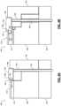
- FIG. 3 Ashows a first example substrate support including a moveable edge ring according to the present disclosure
- FIG. 3 Bshows a second example substrate support including a moveable edge ring according to the present disclosure
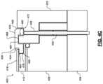
- FIG. 4 Ashows a third example substrate support including a moveable edge ring according to the present disclosure
- FIG. 4 Bshows a fourth example substrate support including a moveable edge ring according to the present disclosure
- FIG. 4 Cshows a fifth example substrate support including a moveable edge ring according to the present disclosure
- FIG. 5 Ashows a sixth example substrate support including a moveable edge ring according to the present disclosure
- FIG. 5 Bshows a seventh example substrate support including a moveable edge ring according to the present disclosure
- FIG. 6 Ashows a bottom view of an example bottom ring of a substrate support according to the present disclosure
- FIG. 6 Bshows a clocking feature of a bottom ring of a substrate support according to the present disclosure
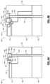
- FIG. 7 Ashows a first example of a bottom ring configured to support a moveable edge ring according to the present disclosure
- FIG. 7 Bshows a second example of a bottom ring configured to support a moveable edge ring according to the present disclosure
- FIG. 7 Cshows a third example of a bottom ring configured to support a moveable edge ring according to the present disclosure
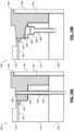
- FIG. 8 Ashows a fourth example of a bottom ring configured to support a moveable edge ring according to the present disclosure
- FIG. 8 Bshows a fifth example of a bottom ring configured to support a moveable edge ring according to the present disclosure
- FIG. 8 Cshows a sixth example of a bottom ring configured to support a moveable edge ring according to the present disclosure
- FIG. 9shows a middle ring configured to support a moveable edge ring according to the present disclosure.
- FIGS. 10 A and 10 Bshow a seventh example of a bottom ring configured to support a moveable edge ring according to the present disclosure.
- a substrate support in a substrate processing systemmay include an edge ring.
- An upper surface of the edge ringmay extend above an upper surface of the substrate support, causing the upper surface of the substrate support (and, in some examples, an upper surface of a substrate arranged on the substrate support) to be recessed relative to the edge ring. This recess may be referred to as a pocket.
- a distance between the upper surface of the edge ring and the upper surface of the substratemay be referred to as a “pocket depth.” Generally, the pocket depth is fixed according to a height of the edge ring relative to the upper surface of the substrate.
- etch processingmay vary due to characteristics of the substrate processing system, the substrate, gas mixtures, etc.
- flow patterns, and therefore an etch rate and etch uniformitymay vary according to the pocket depth of the edge ring, edge ring geometry (i.e., shape), as well as other variables including, but not limited to, gas flow rates, gas species, injection angle, injection position, etc.
- varying the configuration of the edge ringe.g., including edge ring height and/or geometry
- Some substrate processing systemsmay implement moveable (e.g., tunable) edge rings and/or replaceable edge rings.
- a height of a moveable edgemay be adjusted during processing to control etch uniformity.
- the edge ringmay be coupled to an actuator configured to raise and lower the edge ring in response to a controller, user interface, etc.
- a controller of the substrate processing systemcontrols the height of the edge ring during a process, between process steps, etc. according to a particular recipe being performed and associated gas injection parameters.
- edge rings and other componentsmay comprise consumable materials that wear/erode over time. Accordingly, the height of the edge ring may be adjusted to compensate for erosion.
- edge ringsmay be removable and replaceable (e.g., to replace eroded or damaged edge rings, to replace an edge ring with an edge ring having different geometry, etc.).
- substrate processing systems implementing moveable and replaceable edge ringscan be found in U.S. patent application Ser. No. 14/705,430, filed on May 6, 2015, the entire contents of which are incorporated herein by reference.
- Substrate processing systems and methods according to the principles of the present disclosureinclude middle edge rings and bottom edge rings configured to support movable top edge rings.
- the substrate processing system 100may be used for performing etching using RF plasma and/or other suitable substrate processing.
- the substrate processing system 100includes a processing chamber 102 that encloses other components of the substrate processing system 100 and contains the RF plasma.
- the substrate processing chamber 102includes an upper electrode 104 and a substrate support 106 , such as an electrostatic chuck (ESC).
- ESCelectrostatic chuck
- a substrate 108is arranged on the substrate support 106 .
- substrate processing system 100 and chamber 102are shown as an example, the principles of the present disclosure may be applied to other types of substrate processing systems and chambers, such as a substrate processing system that generates plasma in-situ, that implements remote plasma generation and delivery (e.g., using a plasma tube, a microwave tube), etc.
- a substrate processing system that generates plasma in-situthat implements remote plasma generation and delivery (e.g., using a plasma tube, a microwave tube), etc.
- the upper electrode 104may include a gas distribution device such as a showerhead 109 that introduces and distributes process gases (e.g., etch process gases).
- the showerhead 109may include a stem portion including one end connected to a top surface of the processing chamber.
- a base portionis generally cylindrical and extends radially outwardly from an opposite end of the stem portion at a location that is spaced from the top surface of the processing chamber.
- a substrate-facing surface or faceplate of the base portion of the showerheadincludes a plurality of holes through which process gas or purge gas flows.
- the upper electrode 104may include a conducting plate and the process gases may be introduced in another manner.
- the substrate support 106includes a conductive baseplate 110 that acts as a lower electrode.
- the baseplate 110supports a ceramic layer 112 .
- the ceramic layer 112may comprise a heating layer, such as a ceramic multi-zone heating plate.
- a thermal resistance layer 114(e.g., a bond layer) may be arranged between the ceramic layer 112 and the baseplate 110 .
- the baseplate 110may include one or more coolant channels 116 for flowing coolant through the baseplate 110 .
- An RF generating system 120generates and outputs an RF voltage to one of the upper electrode 104 and the lower electrode (e.g., the baseplate 110 of the substrate support 106 ).
- the other one of the upper electrode 104 and the baseplate 110may be DC grounded, AC grounded or floating.
- the RF generating system 120may include an RF voltage generator 122 that generates the RF voltage that is fed by a matching and distribution network 124 to the upper electrode 104 or the baseplate 110 .
- the plasmamay be generated inductively or remotely.
- the RF generating system 120corresponds to a capacitively coupled plasma (CCP) system
- CCPcapacitively coupled plasma
- the principles of the present disclosuremay also be implemented in other suitable systems, such as, for example only transformer coupled plasma (TCP) systems, CCP cathode systems, remote microwave plasma generation and delivery systems, etc.
- a gas delivery system 130includes one or more gas sources 132 - 1 , 132 - 2 , . . . , and 132 -N (collectively gas sources 132 ), where N is an integer greater than zero.
- the gas sourcessupply one or more gases (e.g., etch gas, carrier gases, purge gases, etc.) and mixtures thereof.
- the gas sourcesmay also supply purge gas.
- the gas sources 132are connected by valves 134 - 1 , 134 - 2 , . . . , and 134 -N (collectively valves 134 ) and mass flow controllers 136 - 1 , 136 - 2 , . . .
- a manifold 140An output of the manifold 140 is fed to the processing chamber 102 .
- the output of the manifold 140is fed to the showerhead 109 .
- a temperature controller 142may be connected to a plurality of heating elements, such as thermal control elements (TCEs) 144 arranged in the ceramic layer 112 .
- the heating elements 144may include, but are not limited to, macro heating elements corresponding to respective zones in a multi-zone heating plate and/or an array of micro heating elements disposed across multiple zones of a multi-zone heating plate.
- the temperature controller 142may be used to control the plurality of heating elements 144 to control a temperature of the substrate support 106 and the substrate 108 .
- the temperature controller 142may communicate with a coolant assembly 146 to control coolant flow through the channels 116 .
- the coolant assembly 146may include a coolant pump and reservoir.
- the temperature controller 142operates the coolant assembly 146 to selectively flow the coolant through the channels 116 to cool the substrate support 106 .
- a valve 150 and pump 152may be used to evacuate reactants from the processing chamber 102 .
- a system controller 160may be used to control components of the substrate processing system 100 .
- a robot 170may be used to deliver substrates onto, and remove substrates from, the substrate support 106 .
- the robot 170may transfer substrates between the substrate support 106 and a load lock 172 .
- the temperature controller 142may be implemented within the system controller 160 .
- a protective seal 176may be provided around a perimeter of the bond layer 114 between the ceramic layer 112 and the baseplate 110 .
- the substrate support 106includes an edge ring 180 .
- the edge ring 180may correspond to a top ring, which may be supported by a bottom ring 184 .
- the edge ring 180may be further supported by one or more of a middle ring (not shown in FIG. 1 ), a stepped portion of the ceramic layer 112 , etc. as described below in more detail.
- the edge ring 180is moveable (e.g., moveable upward and downward in a vertical direction) relative to the substrate 108 .
- the edge ring 180may be controlled via an actuator responsive to the controller 160 .
- the edge ring 180may be adjusted during substrate processing (i.e., the edge ring 180 may be a tunable edge ring).
- the edge ring 180may be removable (e.g., using the robot 170 , via an airlock, while the processing chamber 102 is under vacuum).
- the edge ring 180may be both tunable and removable.
- the substrate support 200may include a base or pedestal having an inner portion (e.g., corresponding to an ESC) 208 and an outer portion 212 .
- the outer portion 212may be independent from, and moveable in relation to, the inner portion 208 .
- the outer portion 212may include a bottom ring 216 and a top edge ring 220 .
- the substrate 204is arranged on the inner portion 208 (e.g., on a ceramic layer 224 ) for processing.
- a controller 228communicates with one or more actuators 232 to selectively raise and lower the edge ring 220 .
- the edge ring 220may be raised and/or lowered to adjust a pocket depth of the support 200 during processing.
- the edge ring 220may be raised to facilitate removal and replacement of the edge ring 220 .
- the edge ring 220is shown in a fully lowered position in FIG. 2 A and in a fully raised position in FIG. 2 B .
- the actuators 232correspond to pin actuators configured to selectively extend and retract pins 236 in a vertical direction.
- Other suitable types of actuatorsmay be used in other examples.
- the edge ring 220corresponds to a ceramic or quartz edge ring, although other suitable materials may be used (e.g., silicon carbide, yttria, etc.).
- the controller 228communicates with the actuators 232 to directly raise and lower the edge ring 220 via the pins 236 .
- the inner portion 208is moveable relative to the outer portion 212 .
- the substrate support 300includes an insulator ring or plate 304 and a baseplate (e.g., of an ESC) 308 arranged on the insulator plate 304 .
- the baseplate 308supports a ceramic layer 312 configured to support a substrate 316 arranged thereon for processing.
- the ceramic layer 312has a non-stepped configuration.
- the ceramic layer 312has a stepped configuration.
- the substrate support 300includes a bottom ring 320 that supports an upper (“top”) edge ring 324 .
- One or more vias or guide channels 328may be formed through the insulator plate 304 , the bottom ring 320 , and/or the baseplate 308 to accommodate respective lift pins 332 arranged to selectively raise and lower the edge ring 324 .
- the guide channels 328function as pin alignment holes for respective ones of the lift pins 332 .
- the substrate support 300may further include a middle ring 336 arranged between the bottom ring 320 and the edge ring 324 . In the stepped configuration, the middle ring 336 overlaps the ceramic layer 312 and is arranged to support an outer edge of the substrate 316 .
- the lift pins 332may comprise an erosion-resistant material (e.g., sapphire). An outer surface of the lift pins 332 may be polished smooth to reduce friction between the lift pins 332 and structural features of the bottom ring 320 to facilitate movement.
- one or more ceramic sleeves 340may be arranged in the channels 328 around the lift pins 332 .
- Each of the lift pins 332may include a rounded upper end 344 to minimize contact area between the upper end 344 and the edge ring 324 .
- the smooth outer surface, rounded upper end 344 , guide channel 328 , and/or ceramic sleeves 340facilitate raising and lowering of the edge ring 324 and while preventing binding of the lift pins 332 during movement.
- the bottom ring 320includes a guide feature 348 .
- the middle ring 336includes the guide feature 348 .
- the guide feature 348corresponds to a raised annular rim 352 that extends upward from the bottom ring 320 /the middle ring 336 .
- the guide channels 328 and the lift pins 332extend through the guide feature 348 to engage the edge ring 324 .
- the guide channels 328 and the lift pins 332extend through the bottom ring 320 to engage the edge ring 324 without passing through the middle ring 336 .
- the edge ring 324includes an annular bottom groove 356 arranged to receive the guide feature 348 .
- a profile (i.e., cross-section) shape of the edge ring 324may generally correspond to a “U” shape configured to receive the guide feature 348 , although other suitable shapes may be used.
- the upper surface of the edge ring 324is shown as generally horizontal (i.e., parallel to an upper surface of the substrate support 300 ), the upper surface of the edge ring 324 may have a different profile in other examples.
- the upper surface of the edge ring 324may be tilted or slanted, rounded, etc. In some examples, the upper surface of the edge ring 324 is tilted such that a thickness at an inner diameter of the edge ring 324 is greater than a thickness at an outer diameter of the edge ring 324 to compensate for erosion at the inner diameter.
- a bottom surface of the edge ring 324is configured to be complementary to an upper surface of the bottom ring 320 in FIG. 3 A , or respective surfaces of the bottom ring 320 and the middle ring 336 in FIG. 3 B . Further, an interface 360 between the edge ring 324 and the bottom ring 320 /middle ring 336 is labyrinthine.
- the lower surface of the edge ring 324 and, correspondingly, the interface 360includes multiple changes of direction (e.g., 90 degree changes of direction, upward and downward steps, alternating horizontal and vertical orthogonal paths, etc.) rather than providing a direct (e.g., line of sight) path between the edge ring 324 and the bottom ring 320 /middle ring 336 to interior structures of the substrate support 300 .
- directione.g., 90 degree changes of direction, upward and downward steps, alternating horizontal and vertical orthogonal paths, etc.
- a direct path between the edge ring 324 and the bottom ring 320 /middle ring 336to interior structures of the substrate support 300 .
- likelihood of plasma and process material leakagemay be increased in substrate supports including multiple interfacing rings (e.g., both the top edge ring 324 and one or more of the middle ring 336 and the bottom ring 320 ). This likelihood may be further increased when the moveable edge ring 324 is raised during processing.
- the interface 360includes five changes of direction to restrict access to the guide channels 328 and pins 332 , the ceramic layer 312 , a backside and edge of the substrate 316 , etc.
- the interface 360includes seven changes of direction in a first path 364 and five changes of direction in a second path 368 to restrict access to the guide channels 328 and pins 332 , the ceramic layer 312 , a backside and edge of the substrate 316 , a bond layer 372 , a seal 376 , etc. Accordingly, the interface 360 reduces the likelihood of plasma leakage and light-up, erosion, etc. affecting the interior structures of the substrate support 300 .
- the profile (i.e., cross-section) shape of the edge ring 324(as well as the interfacing surfaces of the bottom ring 320 , middle ring 336 , etc.) is designed to facilitate manufacturing and reduce manufacturing costs.
- walls 380 , 384 of the groove 356 and the guide feature 340may be substantially vertical (e.g., in contrast to being parabolic, trapezoidal, triangular, etc.) to facilitate manufacturing while preventing plasma and process material leakage.
- substantially verticalmay be defined as being perpendicular to upper and/or lower surfaces of the edge ring 324 , within 1° of a normal line of an upper and/or lower surface of the edge ring 324 , parallel to a direction of movement of the edge ring 324 , etc.
- the vertical walls 380 , 384maintain alignment of the edge ring 324 relative to the guide feature 340 during movement of the edge ring 324 .
- respective profiles of the groove 356 and the guide feature 340are parabolic, trapezoidal, triangular, etc.
- upward movement of the edge ring 324causes significant separation between the walls 380 and the walls 384 .
- Edges of the edge ring 324 , the bottom ring 320 , and the middle ring 336 within the interface 360are relatively smooth and continuous to minimize friction between the edge ring 324 and the guide feature 340 during movement of the edge ring 324 .
- respective surfaces of the edge ring 324 , the bottom ring 320 , and the middle ring 336 within the interface 360may undergo additional polishing to achieve a desired surface smoothness.
- surfaces of the edge ring 324 , the bottom ring 320 , and the middle ring 336 within the interface 360may be coated with a material that further reduces friction.
- the surfaces of the edge ring 324 , the bottom ring 320 , and the middle ring 336 within the interface 360may be free of screw holes and/or similar assembly features. In this manner, creation of particles due to contact between surfaces (e.g., during movement of the edge ring 324 ) may be minimized.
- the controller 228 as described in FIGS. 2 A and 2 Bis configured to limit a tunable range of the edge ring 324 according to a height H of the guide feature 348 .
- the tunable rangemay be limited to less than the height H of the guide feature 348 .
- the guide feature 348has a height H of approximately 0.24′′ (e.g., 0.22′′-0.26′′)
- the tunable range of the edge ring 324may be 0.25′′.
- the edge ring 324may be raised from a fully lowered position (e.g., 0.0′′) to a fully raised position (e.g., 0.25′′) without entirely removing the guide feature 348 from the groove 356 in the edge ring 324 . Accordingly, even in the fully raised position, the edge ring 324 still overlaps at least a portion of the guide feature 348 . Limiting the range of the edge ring 324 in this manner retains the labyrinthine interface 360 as described above and prevents lateral misalignment of the edge ring 324 .
- a depth of the groove 356may be approximately equal to (e.g., within 5%) of the height H of the guide feature 348 .
- the depth of the groove 356may be at least 50% of the thickness of the edge ring.
- the tunable range of the edge ring 324 of FIG. 3 Ais 0.15′′ to 0.25′′ and the tunable range of the edge ring 324 of FIG. 3 B is 0.05′′ to 0.15′′.
- a thickness (i.e., height) of the edge ring 324may be between approximately 0.50′′ (e.g., 0.45′′ to 0.55′′) and approximately 0.6′′ (e.g., 0.58′′ to 0.620′′), and a depth of the groove 356 may be approximately 0.30′′ (e.g., 0.29′′ to 0.31′′).
- the “thickness” of the edge ring 324may refer to a thickness of the edge ring 324 at an inner diameter of the edge ring 324 (e.g., a thickness/height of the edge ring 324 at an inner wall 388 ).
- a thickness of the edge ring 324may not be uniform across an upper surface of the edge ring 324 (e.g., the upper surface of the edge ring 324 may be tilted as described above such that a thickness at the inner wall 388 is greater than a thickness at an outer diameter of the edge ring 324 ).
- the edge ring 324may be formed such that the inner wall 388 has at least a predetermined thickness to compensate for the increased erosion at the inner wall 388 .
- the inner wall 388is substantially vertical to avoid contact with the substrate 316 during movement of the edge ring 324 .
- the substrate support 400includes an insulator ring or plate 404 and a baseplate 408 arranged on the insulator plate 404 .
- the baseplate 408supports a ceramic layer 412 configured to support a substrate 416 arranged thereon for processing.
- the ceramic layer 412has a non-stepped configuration.
- the ceramic layer 412has a stepped configuration.
- the substrate support 400includes a bottom ring 420 that supports an upper edge ring 424 . In the stepped configuration, the edge ring 424 overlaps the ceramic layer 412 .
- One or more vias or guide channels 428may be formed through the insulator plate 404 , the bottom ring 420 , and/or the baseplate 408 to accommodate respective lift pins 432 arranged to selectively raise and lower the edge ring 424 .
- the guide channels 428function as pin alignment holes for respective ones of the lift pins 432 .
- the edge rings 424are configured to support an outer edge of the substrate 416 arranged on the ceramic layer 412 .
- inner diameters of the edge rings 424include a step 434 arranged to support the outer edge of the substrate 416 .
- the edge ring 424may be raised and lowered to facilitate removal and replacement of the edge ring 424 buy may not be raised and lowered during processing (i.e., the edge ring 424 is not tunable).
- the edge ring 424may be raised using the lift pins 432 for removal and replacement (e.g., using the robot 170 ).
- a lower, inside corner 436 of the edge ring 424may be chamfered to facilitate alignment (i.e., centering) of the edge ring 424 on the substrate support 400 .
- an upper, outside corner 444 and/or a lower, inside corner 448 of the ceramic layer 412may be chamfered complementarily to the corner 436 . Accordingly, as the edge ring 424 is lowered onto the substrate support 400 , the chamfered corner 436 interacts with the chamfered corner(s) 444 / 448 to cause the edge ring 424 to self-center on the substrate support 400 .
- An upper, outer corner 456 of the edge ring 424may be chamfered to facilitate removal of the edge ring 424 from the processing chamber 102 .
- the edge ring 424is configured to be removed via an airlock.
- airlocksare sized to accommodate substrates of a predetermined size (e.g., 300 mm).
- the edge ring 424has a diameter that is significantly larger than the substrate 416 and a typical edge ring 424 may not fit through the airlock.
- a diameter of the edge ring 424is reduced (e.g., as compared to the edge rings 324 as shown in FIGS. 3 A and 3 B ).
- an outer diameter of the edge ring 324is similar to an outer diameter of the bottom ring 320 .
- an outer diameter of the edge ring 424is significantly less than an outer diameter of the bottom ring 420 .
- an outer diameter of the edge ring 424is less than or equal to approximately 13′′ (e.g., 12.5′′ to 13′′). Chamfering the outer corner 456 further facilitates transfer of the edge ring 424 through the airlock.
- the chamfer of the outer cornermay have a height of 0.050′′ to 0.070′′, a width of 0.030′′ to 0.050′′, and an angle of 25-35°.
- the chamfer of the lower corner 436may have a height of approximately 0.025′′ (e.g., 0.015′′ to 0.040′′), a width of approximately 0.015′′ (e.g., 0.005′′ to 0.030′′), and an angle of approximately 60° (50-70°).
- a thickness (i.e., height) of the edge ring 424is approximately, but not greater than, 0.275′′ (e.g., 0.25′′ to 0.30′′).
- the thickness of the edge ring 424may not exceed a height of an airlock of the processing chamber 102 to allow removal of the edge ring 424 .
- the “thickness” of the edge ring 424may refer to a thickness of the edge ring 424 at an inner diameter of the edge ring 424 (e.g., a thickness/height of the edge ring 424 at an inner wall 458 ) as described above with respect to FIGS. 3 A and 3 B .
- the bottom ring 420includes a guide feature 460 .
- the guide feature 460corresponds to a raised annular rim 464 that extends upward from the bottom ring 420 .
- the guide channels 428 and the lift pins 432extend through the bottom ring 420 to engage the edge ring 424 .
- the edge ring 424includes an annular bottom groove 468 arranged to receive the guide feature 460 .
- a profile of the edge ring 424may generally correspond to a “U” shape configured to receive the guide feature 460 .
- a bottom surface of the edge ring 424 in FIG. 4 Cis configured to be complementary to respective upper surfaces of the bottom ring 420 and the ceramic layer 412 to form a labyrinthine interface 472 .
- the interface 472includes multiple changes of direction (e.g., 90 degree changes of direction) rather than providing a direct path between the edge ring 424 and the bottom ring 420 to interior structures of the substrate support 400 .
- portions of the guide feature 460 , the edge ring 424 , the bottom ring 420 , and/or the ceramic layer 412 within the interface 360may be chamfered to facilitate alignment (i.e., centering) of the edge ring 424 on the substrate support 400 .
- a lower, inside corner 476 of an inner diameter of the edge ring 424 and a corresponding lower, inside corner 480 and/or upper, outside corner 484 of the ceramic layer 412are chamfered.
- mechanical alignment of the guide feature 460 within the groove 468centers the edge ring 324 .
- the chamfer of the lower corner 476may have a height of approximately 0.025′′ (e.g., 0.015′′ to 0.040′′), a width of approximately 0.015′′ (e.g., 0.005′′ to 0.030′′), and an angle of approximately 60° (e.g., 50-60°).
- the substrate support 500includes an insulator ring or plate 504 and a baseplate 508 arranged on the insulator plate 504 .
- the baseplate 508supports a ceramic layer 512 configured to support a substrate 516 arranged thereon for processing.
- the ceramic layer 512has a non-stepped configuration.
- the ceramic layer 512has a stepped configuration.
- the substrate support 500includes a bottom ring 520 that supports an upper edge ring 524 (as shown in FIG. 5 A ) or an upper edge ring 526 (as shown in FIG. 5 B ).
- One or more vias or guide channels 528may be formed through the insulator plate 504 , the bottom ring 520 , and/or the baseplate 508 to accommodate respective lift pins 532 arranged to selectively raise and lower the edge ring 524 / 526 .
- the guide channels 528function as pin alignment holes for respective ones of the lift pins 532 .
- the substrate support 500may further include a middle ring 536 arranged between the bottom ring 520 and the edge ring 526 . In the stepped configuration, the middle ring 536 overlaps the ceramic layer 512 and is arranged to support an outer edge of the substrate 516 .
- FIGS. 5 A and 5 Bcombine features of both the tunable edge rings 324 of FIGS. 3 A and 3 B and the removable/replaceable edge rings of FIGS. 4 A, 4 B, and 4 C .
- the edge ring 526does not extend beneath and support the substrate 516 . Accordingly, the edge ring 524 / 526 may be raised and lowered during processing.
- a tunable range of the edge ring 524 of FIG. 5 Ais 0.05′′ to 0.15′′ and a tunable range of the edge ring 526 of FIG. 5 B is 0.02′′ to 0.05′′.
- an outer diameter of the edge ring 524 / 526is reduced as described with respect to FIGS. 4 A, 4 B, and 4 C to facilitate transfer of the edge ring 524 / 526 through an airlock. Accordingly, the edge ring 524 / 526 may be removed and replaced in situ as described above.
- the bottom ring 520includes a guide feature 540 .
- the middle ring 536includes the guide feature 540 .
- the guide feature 540corresponds to a raised annular rim 544 that extends upward from the bottom ring 520 /the middle ring 536 .
- the guide channels 528 and the lift pins 532extend through the bottom ring 520 to engage the edge ring 524 / 526 .
- the edge ring 524 / 526includes an annular bottom groove 548 arranged to receive the guide feature 540 .
- a profile of the edge ring 524 / 526may generally correspond to a “U” shape configured to receive the guide feature 540 .
- a bottom surface of the edge ring 524 / 526is configured to be complementary to respective upper surfaces of the bottom ring 520 and the middle ring 536 to form a labyrinthine interface 552 .
- the interface 552includes multiple changes of direction (e.g., 90 degree changes of direction) rather than providing a direct path between the edge ring 524 / 526 and the bottom ring 520 to interior structures of the substrate support 500 .
- portions of the guide feature 540 , the edge ring 524 / 526 , the bottom ring 520 , and/or the middle ring 536 within the interface 552may be chamfered to facilitate alignment (i.e., centering) of the edge ring 524 / 526 on the substrate support 500 .
- corners 556 and 558 of the edge ring 524 and complementary corners 560 of the guide feature 540 and 562 of the bottom ring 520are chamfered.
- FIG. 5 Bonly the corner 556 of the edge ring 526 and the corner 560 of the bottom ring 520 are chamfered.
- An upper, outer corner 564 of the edge ring 524may be chamfered to facilitate removal of the edge ring 524 from the processing chamber 102 as described above with respect to FIGS. 4 A, 4 B, and 4 C .
- the chamfers of the lower corners 556 and 558may have a height and width of approximately 0.005′′ to 0.030′′ and an angle of approximately 25 to 35°
- a thickness (i.e., height) of the edge ring 524 / 526may be approximately, but not greater than, 0.25′′ (e.g., 0.25′′ to 0.26′′) and a depth of the groove 548 may be 0.200′′ to 0.220′′.
- a difference between the thickness of the edge ring 524 / 526 and the depth of the groove 548may be not less than 0.075′′.
- the thickness of the edge ring 524 / 526may not exceed a height of an airlock of the processing chamber 102 to allow removal of the edge ring 524 / 526 .
- the thickness of the edge ring 524 / 526may also be maximized, without exceeding the height of the airlock, to optimize tunability of the edge ring 524 / 526 .
- the amount the edge ring 524 / 526 may be raised without needing to be replacedincreases proportionately to the thickness of the edge ring 524 / 526 .
- the “thickness” of the edge ring 524 / 526 as used hereinmay refer to a thickness of the edge ring 524 / 526 at an inner diameter of the edge ring 524 / 526 (e.g., a thickness/height of the edge ring 524 / 526 at an inner wall 568 ) as described above with respect to FIGS. 3 A, 3 B, 4 A, 4 B, and 4 C .
- an example bottom ring 600may implement a clocking feature to facilitate alignment of the bottom ring 600 with an insulator ring 604 .
- the bottom ring 600includes a plurality of guide channels 608 arranged to receive respective lift pins 612 extending through the insulator ring 604 .
- the bottom ring 600further includes one or more clocking features, such as a notch 616 .
- the notch 616is configured to receive a complementary structure, such as a projection 620 , extending upward from the insulator ring 604 . Accordingly, the bottom ring 600 may be installed such that the notch 616 is aligned with and receives the projection 620 to ensure that the guide channels 608 are aligned with respective ones of the lift pins 612 .
- a substrate support 700includes example bottom rings 704 , 708 , and 712 configured to support top moveable edge rings in a non-stepped configuration according to the principles of the present disclosure.
- the bottom ring 704is configured to support the edge ring 324 of FIG. 3 A .
- the bottom ring 708is configured to support the edge ring 424 of FIG. 4 A .
- the bottom ring 712is configured to support the edge ring 524 of FIG. 5 A .
- Respective upper surfaces of each of the bottom rings 704 , 708 , and 712is stepped. In other words, each of the respective upper surfaces has at least two different heights.
- the substrate support 700includes an insulator ring or plate 716 and a baseplate (e.g., of an ESC) 720 arranged on the insulator plate 716 .
- the baseplate 720supports a ceramic layer 724 configured to support a substrate thereon for processing.
- One or more vias or guide channels 728may be formed through the insulator plate 716 and the bottom rings 704 , 708 , 712 to accommodate lift pins 732 arranged to selectively raise and lower the respective edge rings.
- the guide channels 728function as pin alignment holes for respective ones of the lift pins 732 .
- a gap between the lift pins 732 and inner surfaces of the guide channels 728is minimized to decrease plasma leakage.
- a diameter of the guide channels 728is only slightly greater (e.g., 0.005′′-0.010′′ greater) than a diameter of the lift pins 732 .
- the lift pins 732may have a diameter of 0.057′′-0.061′′ while the guide channels 728 have a diameter of 0.063′′-0.067′′.
- the guide channels 728include narrow regions 734 that have a diameter that is less than other portions of the guide channels 728 to further restrict plasma leakage.
- the narrow regions 734may have a diameter that is 0.002-0.004′′ less than the diameter of the guide channels 728 .
- the lift pins 732may include narrow regions located within the narrow regions 734 of the guide channels 728 .
- the bottom ring 704includes a guide feature 736 .
- the guide feature 736corresponds to a raised annular rim 740 that extends upward from the bottom ring 704 .
- the rim 740 and an inner annular rim 742define a groove 744 .
- the guide channels 728 and the lift pins 732extend through the guide feature 736 .
- An upper surface of the bottom ring 704is configured to be complementary to a bottom surface of the edge ring 324 to form a labyrinthine interface including multiple changes of direction as described above.
- Respective widths of the groove 744 and the rim 740are selected to minimize gaps between respective vertical surfaces of the groove 744 and the rim 740 and complementary vertical surfaces on the bottom of the edge ring 324 .
- the gapsmay be less than 0.02′′.
- the bottom ring 712includes a guide feature 746 .
- the guide feature 746corresponds to a raised annular rim 748 that extends upward from the bottom ring 712 .
- the rim 748 and an inner annular rim 750define a first groove 752 while the rim 748 and an outer annular rim 754 define a second groove 756 .
- the guide channels 728 and the lift pins 732extend through the bottom ring 712 .
- An upper surface of the bottom ring 712is configured to be complementary to a bottom surface of the edge ring 524 to form a labyrinthine interface including multiple changes of direction as described above.
- a height of the rim 748is greater than a height of the inner annular rim 750 to facilitate engagement of the rim 748 with the edge ring 524 prior to contact between the inner annular rim 750 and the edge ring 524 .
- portions of the guide feature 746 and/or the bottom ring 712may be chamfered to facilitate alignment (i.e., centering) of the edge ring 524 on the substrate support 700 .
- corners 760 and 764 of the guide feature 746 and corner 768 of the bottom ring 712are chamfered.
- the chamfer of the corner 760may have a height and width of at least approximately 0.008′′ (e.g., 0.007′′ to 0.011′′) and an angle of 15-25°.
- the chamfer of the corner 764may have a height and width of at least approximately 0.01′′ (e.g., 0.01′′ to 0.02′′) and an angle of 20-35°.
- the chamfer of the corner 768may have a height and width of at least approximately 0.010′′ (e.g., 0.010′′ to 0.030′′) and an angle of 20-35°.
- Inner diameters of the bottom rings 704 , 708 , and 712may be at least 11.5′′ (e.g., between 11.5′′ and 11.7′′). Outer diameters of the bottom rings 704 , 708 , and 712 may be no greater than 14′′ (e.g., between 13.8′′ and 14.1′′). Step inner diameters of the bottom rings 708 and 712 at 772 are selected to accommodate the outer diameter of the edge ring 424 or 524 . For example, the outer diameter of the edge ring 424 or 524 may be approximately 12.8′′ (e.g., +/ ⁇ 0.10′′). Accordingly, the inner diameter of the bottom rings 708 and 712 at 772 may be at least 13.0′′.
- a substrate support 800includes example bottom rings 804 , 808 , and 812 configured to support top moveable edge rings in a stepped configuration according to the principles of the present disclosure.
- the bottom ring 804is configured to support the edge ring 324 of FIG. 3 B .
- the bottom ring 808is configured to support the edge ring 424 of FIG. 4 C .
- the bottom ring 812is configured to support the edge ring 526 of FIG. 5 B .
- the bottom rings 804 and 812may be further configured to support the middle ring 336 of FIG. 3 B and the middle ring 536 of FIG. 5 B , respectively.
- Respective upper surfaces of each of the bottom rings 804 , 808 , and 812is stepped. In other words, each of the respective upper surfaces has at least two different heights.
- the substrate support 800includes an insulator ring or plate 816 and a baseplate (e.g., of an ESC) 820 arranged on the insulator plate 816 .
- the baseplate 820supports a ceramic layer 824 configured to support a substrate thereon for processing.
- a bond layer 828may be arranged between the baseplate 820 and the ceramic layer 824 and a seal 832 surrounds the bond layer 828 .
- One or more vias or guide channels 836may be formed through the insulator plate 816 and the bottom rings 804 , 808 , and 812 to accommodate lift pins 840 arranged to selectively raise and lower the respective edge rings.
- the guide channels 836function as pin alignment holes for respective ones of the lift pins 840 .
- a gap between the lift pins 840 and inner surfaces of the guide channels 836is minimized to decrease plasma leakage.
- a diameter of the guide channels 836is only slightly greater (e.g., 0.005′′-0.010′′ greater) than a diameter of the lift pins 840 .
- the lift pins 840may have a diameter of 0.1′′ while the guide channels 836 have a diameter of 0.105′′.
- the guide channels 836include narrow regions 842 that have a diameter that is less than other portions of the guide channels 836 to further restrict plasma leakage.
- the narrow regions 842may have a diameter that is 0.002-0.004′′ less than the diameter of the guide channels 836 .
- one or more ceramic sleeves 844may be arranged in the channels 836 around the lift pins 840 .
- the bottom ring 808includes a guide feature 846 .
- the guide feature 846corresponds to a raised annular rim 848 that extends upward from the bottom ring 808 .
- the rim 848 and an outer annular rim 850define a groove 852 .
- An upper surface of the bottom ring 808is configured to be complementary to a bottom surface of the edge ring 424 to form a labyrinthine interface including multiple changes of direction as described above.
- Respective widths of the groove 852 and the rim 848are selected to minimize gaps between respective vertical surfaces of the groove 852 and the rim 848 and complementary vertical surfaces on the bottom of the edge ring 424 .
- the gapsmay be less than 0.010′′.
- the bottom rings 804 and 812are configured to support the middle rings 336 and 536 having respective guide features 348 and 540 . Accordingly, upper surfaces of the bottom rings 804 and 812 are configured to be, in combination with upper surfaces of the middle rings 336 and 536 , complementary to bottom surfaces of the edge rings 324 and 526 to form a labyrinthine interface including multiple changes of direction as described above.
- the bottom rings 804 , 808 , and 812may be configured to accommodate the ceramic sleeves 844 .
- the bottom rings 804 , 808 , and 812may include a clearance feature such as cavity or cutout 856 having a greater diameter than the guide channels 836 to accommodate upper ends of the ceramic sleeves 844 .
- the bottom rings 804 , 808 , and 812may be installed subsequent to the lift pins 840 .
- respective openings in the bottom rings 804 , 808 , and 812may include a chamfered edge 860 to facilitate installation of the bottom rings 804 , 808 , and 812 over the lift pins 840 .
- the chamfer of the edge 860may have a height and width of 0.020′′ to 0.035′′ and an angle of 40-50°.
- step inner diameters of the bottom rings 808 and 812 at 862are selected to accommodate the outer diameter of the edge rings 424 of FIG. 4 C and 526 of FIG. 5 B .
- the outer diameter of the edge rings 424 and 526may be approximately 12.8′′ (e.g., +/ ⁇ 0.10′′).
- the inner diameters of the bottom rings 808 and 812 at 862may be at least 13.0′′. Accordingly, a gap between the bottom rings 808 and 812 and the outer diameter of the edge rings 424 and 526 can be minimized while still preventing contact between vertical surfaces of the bottom rings 808 and 812 and the edge rings 424 and 526 .
- the bottom ring 808may include a first outer diameter at 864 and a second outer diameter at 868 .
- the second outer diameter 868is greater than the first outer diameter at 864 .
- the substrate support 800may include a liner 872 that protects outer portions of the insulator plate 816 , the baseplate 820 , the bottom ring 808 , etc.
- the liner 872may not protect upper portions of the bottom ring 808 that are exposed to plasma, and increased erosion of the bottom ring 808 in a region adjacent to an upper edge 876 of the baseplate 820 (as indicated by dashed arrow 880 ) may occur.
- the bottom ring 808includes additional material at the second outer diameter 868 to compensate for the increased erosion.
- the middle ring 900may be provided in configurations where the top edge ring would otherwise be supported by upper surfaces of two different components of a substrate support.
- the top edge ringsoverlap both a respective ceramic layer and a respective bottom ring.
- the middle ring 900is arranged to support a portion of the top edge ring that would otherwise by supported by the ceramic layer.
- the middle ring 900is “U”-shaped.
- the middle ring 900includes an inner annular rim 904 and an outer annular rim 908 defining a groove 912 .
- the groove 912is configured to receive a respective top edge ring (e.g., the edge ring 324 or 526 ).
- the outer annular rim 908functions as a guide feature to center the top edge ring 324 or 526 during replacement as described above in FIGS. 3 B and 5 B .
- corners 916 and 920are chamfered to facilitate engagement with the top edge ring.
- the chamfer of the corner 916may have a height and width of at least approximately 0.010′′ (e.g., 0.005′′ to 0.015′′) and an angle of approximately 20° (e.g., 15-25°).
- the chamfer of the corner 920may have a height and width of at least approximately 0.015′′ (e.g., 0.010′′ to 0.020′′) and an angle of approximately 30° (e.g., 25-35°).
- a width of the outer annular rim 908is selected to minimize gaps between respective vertical surfaces of the rim 908 and complementary vertical surfaces on the bottom of the edge ring 324 or 526 .
- the gapsmay be less than 0.010′′ to restrict plasma leakage.
- FIGS. 10 A and 10 Btwo cross-sectional views of a substrate support 1000 illustrate a bottom ring 1004 configured to support top moveable edge rings in a stepped configuration according to the principles of the present disclosure.
- the bottom ring 1004is configured to support an edge ring (e.g., 526 ) in a configuration similar to that shown in FIGS. 5 B and 8 C .
- the bottom ring 1004may be further configured to support a middle ring in a configuration similar to that shown in FIG. 5 B .
- the substrate support 1000includes an insulator ring or plate 1008 and a baseplate (e.g., of an ESC) 1012 arranged on the insulator plate 1008 .
- the baseplate 1012supports a ceramic layer 1016 configured to support a substrate thereon for processing.
- a bond layer 1020may be arranged between the baseplate 1012 and the ceramic layer 1016 and a seal 1024 surrounds the bond layer 1020 .
- one or more vias or guide channels 1028may be formed through the insulator plate 1008 , the baseplate 1012 , and the bottom ring 1004 to accommodate lift pins 1032 arranged to selectively raise and lower the edge ring.
- the guide channels 1028function as pin alignment holes for respective ones of the lift pins 1032 .
- a gap between the lift pins 1032 and inner surfaces of the guide channels 1028is minimized to decrease plasma leakage.
- a diameter of the guide channels 1028is only slightly greater (e.g., 0.005′′-0.010′′ greater) than a diameter of the lift pins 1032 .
- the lift pins 1032may have a diameter of 0.1′′ while the guide channels 1028 have a diameter of 0.105′′.
- the guide channels 1028include narrow regions 1036 that have a diameter that is less than other portions of the guide channels 1028 to further restrict plasma leakage.
- the narrow regions 1036may have a diameter that is 0.002-0.004′′ less than the diameter of the guide channels 1028 .
- one or more ceramic sleeves 1040may be arranged in the channels 1028 around the lift pins 1032 .
- the substrate support 1000may include a liner 1044 arranged to enclose and protect components of the substrate support 1000 such as the insulator plate 1008 , the baseplate 1012 , and the bottom ring 1004 .
- the bottom ring 1004 as shown in FIGS. 10 A and 10 Bincludes an annular lip 1048 extending radially outward from the bottom ring 1004 above the liner 1044 .
- the lip 1048facilitates installation and removal of the bottom ring 1004 when the liner 1044 is present.
- the baseplate 1012may be coupled to the insulator plate 1008 using bolts 1052 inserted through respective bolt mounting holes 1056 .
- Ceramic plugs 1060are arranged above the bolts 1052 to prevent plasma leakage in the bolt mounting holes 1056 and between the bottom ring 1004 and the baseplate 1012 .
- the bottom ring 1004 as shown in FIG. 10 Bincludes clearance features such as cavities or cutouts 1064 to accommodate the ceramic plugs 1060 .
- Spatial and functional relationships between elementsare described using various terms, including “connected,” “engaged,” “coupled,” “adjacent,” “next to,” “on top of,” “above,” “below,” and “disposed.” Unless explicitly described as being “direct,” when a relationship between first and second elements is described in the above disclosure, that relationship can be a direct relationship where no other intervening elements are present between the first and second elements, but can also be an indirect relationship where one or more intervening elements are present (either spatially or functionally) between the first and second elements.
- the phrase at least one of A, B, and Cshould be construed to mean a logical (A OR B OR C), using a non-exclusive logical OR, and should not be construed to mean “at least one of A, at least one of B, and at least one of C.”
- a controlleris part of a system, which may be part of the above-described examples.
- Such systemscan comprise semiconductor processing equipment, including a processing tool or tools, chamber or chambers, a platform or platforms for processing, and/or specific processing components (a wafer pedestal, a gas flow system, etc.).
- These systemsmay be integrated with electronics for controlling their operation before, during, and after processing of a semiconductor wafer or substrate.
- the electronicsmay be referred to as the “controller,” which may control various components or subparts of the system or systems.
- the controllermay be programmed to control any of the processes disclosed herein, including the delivery of processing gases, temperature settings (e.g., heating and/or cooling), pressure settings, vacuum settings, power settings, radio frequency (RF) generator settings, RF matching circuit settings, frequency settings, flow rate settings, fluid delivery settings, positional and operation settings, wafer transfers into and out of a tool and other transfer tools and/or load locks connected to or interfaced with a specific system.
- temperature settingse.g., heating and/or cooling
- RFradio frequency
- the controllermay be defined as electronics having various integrated circuits, logic, memory, and/or software that receive instructions, issue instructions, control operation, enable cleaning operations, enable endpoint measurements, and the like.
- the integrated circuitsmay include chips in the form of firmware that store program instructions, digital signal processors (DSPs), chips defined as application specific integrated circuits (ASICs), and/or one or more microprocessors, or microcontrollers that execute program instructions (e.g., software).
- Program instructionsmay be instructions communicated to the controller in the form of various individual settings (or program files), defining operational parameters for carrying out a particular process on or for a semiconductor wafer or to a system.
- the operational parametersmay, in some embodiments, be part of a recipe defined by process engineers to accomplish one or more processing steps during the fabrication of one or more layers, materials, metals, oxides, silicon, silicon dioxide, surfaces, circuits, and/or dies of a wafer.
- the controllermay be a part of or coupled to a computer that is integrated with the system, coupled to the system, otherwise networked to the system, or a combination thereof.
- the controllermay be in the “cloud” or all or a part of a fab host computer system, which can allow for remote access of the wafer processing.
- the computermay enable remote access to the system to monitor current progress of fabrication operations, examine a history of past fabrication operations, examine trends or performance metrics from a plurality of fabrication operations, to change parameters of current processing, to set processing steps to follow a current processing, or to start a new process.
- a remote computere.g. a server
- the remote computermay include a user interface that enables entry or programming of parameters and/or settings, which are then communicated to the system from the remote computer.
- the controllerreceives instructions in the form of data, which specify parameters for each of the processing steps to be performed during one or more operations. It should be understood that the parameters may be specific to the type of process to be performed and the type of tool that the controller is configured to interface with or control.
- the controllermay be distributed, such as by comprising one or more discrete controllers that are networked together and working towards a common purpose, such as the processes and controls described herein.
- An example of a distributed controller for such purposeswould be one or more integrated circuits on a chamber in communication with one or more integrated circuits located remotely (such as at the platform level or as part of a remote computer) that combine to control a process on the chamber.
- example systemsmay include a plasma etch chamber or module, a deposition chamber or module, a spin-rinse chamber or module, a metal plating chamber or module, a clean chamber or module, a bevel edge etch chamber or module, a physical vapor deposition (PVD) chamber or module, a chemical vapor deposition (CVD) chamber or module, an atomic layer deposition (ALD) chamber or module, an atomic layer etch (ALE) chamber or module, an ion implantation chamber or module, a track chamber or module, and any other semiconductor processing systems that may be associated or used in the fabrication and/or manufacturing of semiconductor wafers.
- PVDphysical vapor deposition
- CVDchemical vapor deposition
- ALDatomic layer deposition
- ALEatomic layer etch
- the controllermight communicate with one or more of other tool circuits or modules, other tool components, cluster tools, other tool interfaces, adjacent tools, neighboring tools, tools located throughout a factory, a main computer, another controller, or tools used in material transport that bring containers of wafers to and from tool locations and/or load ports in a semiconductor manufacturing factory.
Landscapes
- Engineering & Computer Science (AREA)
- Physics & Mathematics (AREA)
- Computer Hardware Design (AREA)
- Power Engineering (AREA)
- Microelectronics & Electronic Packaging (AREA)
- Condensed Matter Physics & Semiconductors (AREA)
- General Physics & Mathematics (AREA)
- Manufacturing & Machinery (AREA)
- Analytical Chemistry (AREA)
- Chemical & Material Sciences (AREA)
- Plasma & Fusion (AREA)
- Health & Medical Sciences (AREA)
- Toxicology (AREA)
- Container, Conveyance, Adherence, Positioning, Of Wafer (AREA)
- Drying Of Semiconductors (AREA)
- Chemical Vapour Deposition (AREA)
- Other Investigation Or Analysis Of Materials By Electrical Means (AREA)
Abstract
Description
Claims (8)
Priority Applications (2)
| Application Number | Priority Date | Filing Date | Title |
|---|---|---|---|
| US17/681,606US12183554B2 (en) | 2017-11-21 | 2022-02-25 | Bottom and middle edge rings |
| US18/990,129US20250132135A1 (en) | 2017-11-21 | 2024-12-20 | Bottom and middle edge rings |
Applications Claiming Priority (3)
| Application Number | Priority Date | Filing Date | Title |
|---|---|---|---|
| PCT/US2017/062769WO2019103722A1 (en) | 2017-11-21 | 2017-11-21 | Bottom and middle edge rings |
| US201916487703A | 2019-08-21 | 2019-08-21 | |
| US17/681,606US12183554B2 (en) | 2017-11-21 | 2022-02-25 | Bottom and middle edge rings |
Related Parent Applications (2)
| Application Number | Title | Priority Date | Filing Date |
|---|---|---|---|
| US16/487,703DivisionUS12237154B2 (en) | 2017-11-21 | 2017-11-21 | Bottom and middle edge rings |
| PCT/US2017/062769DivisionWO2019103722A1 (en) | 2017-11-21 | 2017-11-21 | Bottom and middle edge rings |
Related Child Applications (1)
| Application Number | Title | Priority Date | Filing Date |
|---|---|---|---|
| US18/990,129ContinuationUS20250132135A1 (en) | 2017-11-21 | 2024-12-20 | Bottom and middle edge rings |
Publications (2)
| Publication Number | Publication Date |
|---|---|
| US20220189744A1 US20220189744A1 (en) | 2022-06-16 |
| US12183554B2true US12183554B2 (en) | 2024-12-31 |
Family
ID=66631121
Family Applications (4)
| Application Number | Title | Priority Date | Filing Date |
|---|---|---|---|
| US16/487,703Active2039-01-06US12237154B2 (en) | 2017-11-21 | 2017-11-21 | Bottom and middle edge rings |
| US17/681,606ActiveUS12183554B2 (en) | 2017-11-21 | 2022-02-25 | Bottom and middle edge rings |
| US17/681,633PendingUS20220189745A1 (en) | 2017-11-21 | 2022-02-25 | Bottom and middle edge rings |
| US18/990,129PendingUS20250132135A1 (en) | 2017-11-21 | 2024-12-20 | Bottom and middle edge rings |
Family Applications Before (1)
| Application Number | Title | Priority Date | Filing Date |
|---|---|---|---|
| US16/487,703Active2039-01-06US12237154B2 (en) | 2017-11-21 | 2017-11-21 | Bottom and middle edge rings |
Family Applications After (2)
| Application Number | Title | Priority Date | Filing Date |
|---|---|---|---|
| US17/681,633PendingUS20220189745A1 (en) | 2017-11-21 | 2022-02-25 | Bottom and middle edge rings |
| US18/990,129PendingUS20250132135A1 (en) | 2017-11-21 | 2024-12-20 | Bottom and middle edge rings |
Country Status (7)
| Country | Link |
|---|---|
| US (4) | US12237154B2 (en) |
| EP (3) | EP3843129B1 (en) |
| JP (5) | JP6878616B2 (en) |
| KR (6) | KR102401722B1 (en) |
| CN (6) | CN118380371A (en) |
| SG (1) | SG11201907515WA (en) |
| WO (1) | WO2019103722A1 (en) |
Cited By (1)
| Publication number | Priority date | Publication date | Assignee | Title |
|---|---|---|---|---|
| US12400839B2 (en)* | 2023-05-04 | 2025-08-26 | Samsung Electronics Co., Ltd. | Focus ring and apparatus for processing a substrate including the same |
Families Citing this family (19)
| Publication number | Priority date | Publication date | Assignee | Title |
|---|---|---|---|---|
| US10658222B2 (en) | 2015-01-16 | 2020-05-19 | Lam Research Corporation | Moveable edge coupling ring for edge process control during semiconductor wafer processing |
| CN118380371A (en)* | 2017-11-21 | 2024-07-23 | 朗姆研究公司 | Bottom edge ring and middle edge ring |
| JP7140610B2 (en)* | 2018-09-06 | 2022-09-21 | 株式会社日立ハイテク | Plasma processing equipment |
| JP7105666B2 (en)* | 2018-09-26 | 2022-07-25 | 東京エレクトロン株式会社 | Plasma processing equipment |
| US20220235459A1 (en)* | 2019-06-18 | 2022-07-28 | Lam Research Corporation | Reduced diameter carrier ring hardware for substrate processing systems |
| TWM602283U (en)* | 2019-08-05 | 2020-10-01 | 美商蘭姆研究公司 | Edge ring with lift pin grooves for a substrate processing system |
| WO2021025934A1 (en) | 2019-08-05 | 2021-02-11 | Lam Research Corporation | Edge ring systems for substrate processing systems |
| JP2022544494A (en)* | 2019-08-14 | 2022-10-19 | ラム リサーチ コーポレーション | Movable edge ring for substrate processing system |
| KR102747645B1 (en)* | 2019-10-10 | 2024-12-27 | 삼성전자주식회사 | Electro-static chuck and substrate processing apparatus including the same |
| TW202147371A (en) | 2020-02-04 | 2021-12-16 | 美商蘭姆研究公司 | Electrostatic edge ring mounting system for substrate processing |
| GB202002798D0 (en)* | 2020-02-27 | 2020-04-15 | Lam Res Ag | Apparatus for processing a wafer |
| KR102848914B1 (en) | 2020-05-07 | 2025-08-21 | 엘지전자 주식회사 | Laundry Treatment Apparatus |
| US11600516B2 (en)* | 2020-05-13 | 2023-03-07 | Asmpt Singapore Pte. Ltd. | Die ejector height adjustment |
| US12381029B2 (en)* | 2020-09-25 | 2025-08-05 | Intel Corporation | Stepped coax MIL PTHS for modulating inductance within a package |
| CN112397366B (en)* | 2020-11-05 | 2023-07-14 | 北京北方华创微电子装备有限公司 | Bearing device and semiconductor reaction chamber |
| KR20230027251A (en)* | 2020-11-19 | 2023-02-27 | 어플라이드 머티어리얼스, 인코포레이티드 | Rings for board extreme edge protection |
| KR102327270B1 (en) | 2020-12-03 | 2021-11-17 | 피에스케이 주식회사 | Support unit, apparatus for treating a substrate and method for treating a substrate |
| KR102427214B1 (en)* | 2021-11-12 | 2022-08-01 | 비씨엔씨 주식회사 | A focus ring assembly for semiconductors that can be combined and disassembled |
| KR20240112341A (en)* | 2021-12-03 | 2024-07-18 | 램 리써치 코포레이션 | Wide coverage edge ring for enhanced shielding of substrate processing systems |
Citations (445)
| Publication number | Priority date | Publication date | Assignee | Title |
|---|---|---|---|---|
| US3534753A (en) | 1968-03-18 | 1970-10-20 | Veriflo Corp | Ratio controller for gases |
| US4262686A (en) | 1978-07-20 | 1981-04-21 | Dragerwerk Aktiengesellschaft | Apparatus for the electrically controlled proportioning and mixing of gases |
| US4374698A (en) | 1980-07-11 | 1983-02-22 | U.S. Philips Corporation | Method of manufacturing a semiconductor device |
| US4431477A (en) | 1983-07-05 | 1984-02-14 | Matheson Gas Products, Inc. | Plasma etching with nitrous oxide and fluoro compound gas mixture |
| US4793897A (en) | 1987-03-20 | 1988-12-27 | Applied Materials, Inc. | Selective thin film etch process |
| EP0424299A2 (en) | 1989-10-20 | 1991-04-24 | International Business Machines Corporation | Selective silicon nitride plasma etching |
| US5190823A (en) | 1989-07-31 | 1993-03-02 | General Electric Company | Method for improving adhesion of synthetic diamond coatings to substrates |
| US5220515A (en) | 1991-04-22 | 1993-06-15 | Applied Materials, Inc. | Flow verification for process gas in a wafer processing system apparatus and method |
| US5304248A (en) | 1990-12-05 | 1994-04-19 | Applied Materials, Inc. | Passive shield for CVD wafer processing which provides frontside edge exclusion and prevents backside depositions |
| US5329965A (en) | 1993-07-30 | 1994-07-19 | The Perkin-Elmer Corporation | Hybrid valving system for varying fluid flow rate |
| US5346578A (en) | 1992-11-04 | 1994-09-13 | Novellus Systems, Inc. | Induction plasma source |
| US5376214A (en) | 1992-09-22 | 1994-12-27 | Nissan Motor Co., Ltd. | Etching device |
| US5413145A (en) | 1993-04-19 | 1995-05-09 | Texaco Inc. | Low-pressure-drop critical flow venturi |
| US5520969A (en) | 1994-02-04 | 1996-05-28 | Applied Materials, Inc. | Method for in-situ liquid flow rate estimation and verification |
| US5569350A (en) | 1994-03-18 | 1996-10-29 | Anelva Corporation | Mechanism and method for mechanically removing a substrate |
| US5605179A (en) | 1995-03-17 | 1997-02-25 | Insync Systems, Inc. | Integrated gas panel |
| US5660673A (en) | 1993-08-31 | 1997-08-26 | Nec Corporation | Apparatus for dry etching |
| US5662143A (en) | 1996-05-16 | 1997-09-02 | Gasonics International | Modular gas box system |
| US5683517A (en) | 1995-06-07 | 1997-11-04 | Applied Materials, Inc. | Plasma reactor with programmable reactant gas distribution |
| US5702530A (en) | 1995-06-23 | 1997-12-30 | Applied Materials, Inc. | Distributed microwave plasma reactor for semiconductor processing |
| EP0821404A2 (en) | 1996-07-24 | 1998-01-28 | Applied Materials, Inc. | Lift pin and support pin apparatus for a processing chamber |
| US5744695A (en) | 1997-01-10 | 1998-04-28 | Sony Corporation | Apparatus to check calibration of mass flow controllers |
| EP0838842A2 (en) | 1996-10-23 | 1998-04-29 | Applied Materials, Inc. | Plasma reactor with heated source of a polymer-hardening precursor material |
| US5762714A (en) | 1994-10-18 | 1998-06-09 | Applied Materials, Inc. | Plasma guard for chamber equipped with electrostatic chuck |
| CN1189859A (en) | 1995-07-10 | 1998-08-05 | 沃特金斯·约翰逊公司 | Plasma enhanced chemical processing reactor and method |
| JPH10280173A (en) | 1997-02-06 | 1998-10-20 | Matsushita Electric Ind Co Ltd | Etching method and etching apparatus |
| EP0875979A1 (en) | 1997-05-02 | 1998-11-04 | FHP Motors GmbH | Attachment device for the stator winding an electrical motor |
| US5840129A (en) | 1994-07-15 | 1998-11-24 | Ontrak Systems, Inc. | Hesitation free roller |
| US5907221A (en) | 1995-08-16 | 1999-05-25 | Applied Materials, Inc. | Inductively coupled plasma reactor with an inductive coil antenna having independent loops |
| US5952060A (en) | 1996-06-14 | 1999-09-14 | Applied Materials, Inc. | Use of carbon-based films in extending the lifetime of substrate processing system components |
| US6022809A (en) | 1998-12-03 | 2000-02-08 | Taiwan Semiconductor Manufacturing Company, Ltd. | Composite shadow ring for an etch chamber and method of using |
| US6042687A (en) | 1997-06-30 | 2000-03-28 | Lam Research Corporation | Method and apparatus for improving etch and deposition uniformity in plasma semiconductor processing |
| US6044534A (en) | 1995-12-07 | 2000-04-04 | Nec Corporation | Semiconductor device manufacturing machine and method for manufacturing a semiconductor device by using the same manufacturing machine |
| US6048403A (en) | 1998-04-01 | 2000-04-11 | Applied Materials, Inc. | Multi-ledge substrate support for a thermal processing chamber |
| US6050283A (en) | 1995-07-07 | 2000-04-18 | Air Liquide America Corporation | System and method for on-site mixing of ultra-high-purity chemicals for semiconductor processing |
| JP2000124141A (en) | 1998-10-19 | 2000-04-28 | Applied Materials Inc | Semiconductor manufacturing equipment |
| US6060400A (en) | 1998-03-26 | 2000-05-09 | The Research Foundation Of State University Of New York | Highly selective chemical dry etching of silicon nitride over silicon and silicon dioxide |
| US6062256A (en) | 1997-02-11 | 2000-05-16 | Engineering Measurements Company | Micro mass flow control apparatus and method |
| US6074959A (en) | 1997-09-19 | 2000-06-13 | Applied Materials, Inc. | Method manifesting a wide process window and using hexafluoropropane or other hydrofluoropropanes to selectively etch oxide |
| WO2000040776A1 (en) | 1999-01-05 | 2000-07-13 | Ronal Systems Corporation | In situ chemical generator and method |
| US6152168A (en) | 1997-08-15 | 2000-11-28 | Fujikin Incorporated | Pressure-type flow rate control apparatus |
| WO2001013404A1 (en) | 1999-08-16 | 2001-02-22 | Applied Materials, Inc. | Diamond coated parts in a plasma reactor |
| US6206976B1 (en) | 1999-08-27 | 2001-03-27 | Lucent Technologies Inc. | Deposition apparatus and related method with controllable edge exclusion |
| US6210593B1 (en) | 1997-02-06 | 2001-04-03 | Matsushita Electric Industrial Co., Ltd. | Etching method and etching apparatus |
| US6217937B1 (en) | 1998-07-15 | 2001-04-17 | Cornell Research Foundation, Inc. | High throughput OMVPE apparatus |
| US6231716B1 (en) | 1998-11-09 | 2001-05-15 | Applied Materials, Inc. | Processing chamber with rapid wafer exchange |
| US20010002581A1 (en) | 1998-09-03 | 2001-06-07 | Kazuyasu Nishikawa | System for manufacturing a semiconductor device |
| US20010004903A1 (en) | 1999-04-16 | 2001-06-28 | Tadahiro Ohmi | Parallel divided flow-type fluid supply apparatus, and fluid-switchable pressure-type flow control method and fluid-switchable pressure-type flow control system for the same fluid supply apparatus |
| US20010013363A1 (en) | 1999-04-22 | 2001-08-16 | Hirofumi Kitayama | Apparatus and method for feeding gases for use in semiconductor manufacturing |
| JP2001230239A (en) | 2000-02-15 | 2001-08-24 | Tokyo Electron Ltd | Apparatus and method for treating |
| US6294466B1 (en) | 1998-05-01 | 2001-09-25 | Applied Materials, Inc. | HDP-CVD apparatus and process for depositing titanium films for semiconductor devices |
| US20010035530A1 (en) | 2000-04-26 | 2001-11-01 | Takashi Udagawa | Vapor phase deposition system |
| JP2001522142A (en) | 1997-11-03 | 2001-11-13 | エーエスエム アメリカ インコーポレイテッド | Improved low mass wafer support system |
| US6328808B1 (en) | 1997-08-19 | 2001-12-11 | Applied Materials, Inc. | Apparatus and method for aligning and controlling edge deposition on a substrate |
| JP2002500439A (en) | 1997-12-23 | 2002-01-08 | ユナキス・バルツェルス・アクチェンゲゼルシャフト | Holding device |
| JP2002503765A (en) | 1998-02-13 | 2002-02-05 | アプライド マテリアルズ インコーポレイテッド | Reactor for chemical vapor deposition |
| US20020038669A1 (en) | 2000-10-04 | 2002-04-04 | Takayuki Yamagishi | Gas-line system for semiconductor-manufacturing apparatus |
| US20020042205A1 (en) | 2000-10-06 | 2002-04-11 | Mcmillin Brian K. | Gas distribution apparatus for semiconductor processing |
| US20020045265A1 (en) | 2000-03-07 | 2002-04-18 | Bergh H. Sam | Parallel flow reactor having variable composition |
| US6376386B1 (en) | 1997-02-25 | 2002-04-23 | Fujitsu Limited | Method of etching silicon nitride by a mixture of CH2 F2, CH3F or CHF3 and an inert gas |
| US20020046991A1 (en) | 1997-06-26 | 2002-04-25 | Smith Donald K. | Toroidal low-field reactive gas source |
| US20020048536A1 (en) | 1999-03-03 | 2002-04-25 | Bergh H. Sam | Parallel flow process optimization reactors |
| KR20020031417A (en) | 1999-10-29 | 2002-05-01 | 조셉 제이. 스위니 | Semiconductor-manufacturing apparatus |
| US20020067585A1 (en) | 2000-06-02 | 2002-06-06 | Nikon Corporation | Electrostatic wafer chucks and charged-particle-beam exposure apparatus comprising same |
| US20020072240A1 (en) | 2000-12-07 | 2002-06-13 | Semiconductor Leading Edge Technologies, Inc. | Plasma etching apparatus with focus ring and plasma etching method |
| US20020071128A1 (en) | 1996-02-16 | 2002-06-13 | Doan Trung T. | Endpoint detector and method for measuring a change in wafer thickness in chemical-mechanical polishing of semiconductor wafers and other microelectronic substrates |
| US20020088542A1 (en) | 1999-07-07 | 2002-07-11 | Kazuyasu Nishikawa | Plasma processing apparatus |
| JP2002217171A (en) | 2001-01-17 | 2002-08-02 | Sony Corp | Etching equipment |
| JP2002231794A (en) | 2001-02-02 | 2002-08-16 | Tokyo Electron Ltd | Mechanism of placing workpiece |
| KR20020071398A (en) | 2001-03-06 | 2002-09-12 | 삼성전자 주식회사 | Apparatus for dry etching in semiconductor device processing |
| TW506234B (en) | 2000-09-18 | 2002-10-11 | Tokyo Electron Ltd | Tunable focus ring for plasma processing |
| US20020160125A1 (en) | 1999-08-17 | 2002-10-31 | Johnson Wayne L. | Pulsed plasma processing method and apparatus |
| US20020174905A1 (en) | 2001-04-20 | 2002-11-28 | Festo Corporation | Stackable valve manifold arrangement |
| US20020175144A1 (en) | 1999-03-25 | 2002-11-28 | Hoiman(Raymond) Hung | Enhancement of silicon oxide etch rate and nitride selectivity using hexafluorobutadiene or other heavy perfluorocarbon |
| US6492774B1 (en) | 2000-10-04 | 2002-12-10 | Lam Research Corporation | Wafer area pressure control for plasma confinement |
| US20030000369A1 (en) | 2001-06-27 | 2003-01-02 | Yamaha Corporation | Apparatus for delivering music performance information via communication network and apparatus for receiving and reproducing delivered music performance information |
| US20030003696A1 (en) | 2001-06-29 | 2003-01-02 | Avgerinos Gelatos | Method and apparatus for tuning a plurality of processing chambers |
| US20030013080A1 (en) | 2001-06-25 | 2003-01-16 | Luebke Kevin J. | Complex multicellular assemblies ex vivo |
| US20030011619A1 (en) | 1997-10-08 | 2003-01-16 | Robert S. Jacobs | Synchronization and blending of plural images into a seamless combined image |
| US20030015141A1 (en) | 2000-04-28 | 2003-01-23 | Yoji Takagi | Wafer supporting device in semiconductor manufacturing device |
| US20030021356A1 (en) | 2001-07-13 | 2003-01-30 | Murata Manufacturing Co., Ltd. | Composite high-frequency switch, high-frequency module, and communication apparatus |
| US20030023023A1 (en) | 1999-12-10 | 2003-01-30 | Shearwater Corporation | Hydrolytically degradable polymers and hydrogels made therefrom |
| US20030116195A1 (en) | 2001-12-21 | 2003-06-26 | Agilent Technologies, Inc. | Method for the provision of fluid volume streams |
| US6589352B1 (en) | 1999-12-10 | 2003-07-08 | Applied Materials, Inc. | Self aligning non contact shadow ring process kit |
| US20030130807A1 (en) | 2002-01-04 | 2003-07-10 | Jesse Ambrosina | Mass flow ratio system and method |
| TW200302035A (en) | 2001-12-13 | 2003-07-16 | Tokyo Electron Ltd | Ring mechanism, and plasma processing device using the ring mechanism |
| KR20030065126A (en) | 2002-01-31 | 2003-08-06 | (주) 엠큐브테크놀로지 | System for cooling stimulus coil for use in equipment using magnetic field |
| US6605352B1 (en) | 2000-01-06 | 2003-08-12 | Saint-Gobain Ceramics & Plastics, Inc. | Corrosion and erosion resistant thin film diamond coating and applications therefor |
| US6623597B1 (en)* | 1999-09-29 | 2003-09-23 | Samsung Electronics Co., Ltd. | Focus ring and apparatus for processing a semiconductor wafer comprising the same |
| US20030186563A1 (en) | 2002-03-25 | 2003-10-02 | Dainippon Screen Mfg. Co., Ltd. | Thermal processing apparatus and thermal processing method |
| US20030196890A1 (en)* | 2002-04-19 | 2003-10-23 | Applied Materials, Inc. | Reducing particle generation during sputter deposition |
| US20030213560A1 (en) | 2002-05-16 | 2003-11-20 | Yaxin Wang | Tandem wafer processing system and process |
| US20030230239A1 (en) | 2002-06-17 | 2003-12-18 | Applied Materials, Inc. | Gas flow division in a wafer processing system having multiple chambers |
| US20030231950A1 (en) | 2002-06-12 | 2003-12-18 | Ivo Raaijmakers | Semiconductor wafer position shift measurement and correction |
| US20030236643A1 (en) | 2002-06-24 | 2003-12-25 | Ali Shajii | Apparatus and method for calibration of mass flow controller |
| US20030236638A1 (en) | 2002-06-24 | 2003-12-25 | Ali Shajii | Apparatus and method for displaying mass flow controller pressure |
| US20030236592A1 (en) | 2002-06-24 | 2003-12-25 | Ali Shajii | Apparatus and method for mass flow controller with network access to diagnostics |
| US20040007176A1 (en) | 2002-07-15 | 2004-01-15 | Applied Materials, Inc. | Gas flow control in a wafer processing system having multiple chambers for performing same process |
| US20040025060A1 (en) | 2001-02-19 | 2004-02-05 | Hewlett-Packard Company | Process for executing a downloadable service receiving restrictive access rights to at least one profile file |
| US20040026149A1 (en) | 2000-09-19 | 2004-02-12 | Wilkinson Donald Raymond | Occupant restraint |
| US20040031338A1 (en) | 2002-08-13 | 2004-02-19 | Taiwan Semiconductor Manufacturing Co., Ltd. | Chamber wafer detection |
| US20040053428A1 (en) | 2002-09-18 | 2004-03-18 | Steger Robert J. | Method and apparatus for the compensation of edge ring wear in a plasma processing chamber |
| US6709547B1 (en) | 1999-06-30 | 2004-03-23 | Lam Research Corporation | Moveable barrier for multiple etch processes |
| US20040060595A1 (en) | 2002-09-26 | 2004-04-01 | John Chittenden | Method and apparatus for dividing the flow of a gas stream |
| US6722642B1 (en) | 2002-11-06 | 2004-04-20 | Tokyo Electron Limited | High pressure compatible vacuum chuck for semiconductor wafer including lift mechanism |
| US20040089240A1 (en) | 2002-04-24 | 2004-05-13 | Dando Ross S. | Chemical vapor deposition apparatus |
| US6736931B2 (en) | 1991-06-27 | 2004-05-18 | Kenneth S. Collins | Inductively coupled RF plasma reactor and plasma chamber enclosure structure therefor |
| US20040094206A1 (en) | 2002-11-15 | 2004-05-20 | Renesas Technology Corp. | Semiconductor manufacturing apparatus enabling inspection of mass flow controller maintaining connection thereto |
| US6744212B2 (en) | 2002-02-14 | 2004-06-01 | Lam Research Corporation | Plasma processing apparatus and method for confining an RF plasma under very high gas flow and RF power density conditions |
| KR20040050080A (en) | 2002-12-09 | 2004-06-16 | 주식회사 하이닉스반도체 | Apparatus for driving focus ring of plasma etch chamber |
| US20040112540A1 (en) | 2002-12-13 | 2004-06-17 | Lam Research Corporation | Uniform etch system |
| US20040112538A1 (en) | 2002-12-13 | 2004-06-17 | Lam Research Corporation | Gas distribution system with tuning gas |
| US20040149389A1 (en) | 2002-11-26 | 2004-08-05 | Tokyo Electron Limited | Plasma processing device |
| US20040163601A1 (en) | 2003-02-26 | 2004-08-26 | Masanori Kadotani | Plasma processing apparatus |
| US20040168719A1 (en) | 2003-02-28 | 2004-09-02 | Masahiro Nambu | System for dividing gas flow |
| US20040173270A1 (en) | 2003-03-03 | 2004-09-09 | Harris James M. | Fluid delivery system and mounting panel therefor |
| JP2004266127A (en) | 2003-03-03 | 2004-09-24 | Kawasaki Microelectronics Kk | Quartz tool and its manufacturing method |
| US20040200529A1 (en) | 2001-05-24 | 2004-10-14 | Celerity Group, Inc. | Method and apparatus for providing a determined ratio of process fluids |
| JP2004296553A (en) | 2003-03-25 | 2004-10-21 | Ngk Insulators Ltd | Structural for semiconductor manufacturing equipment |
| US6818560B1 (en) | 1999-09-22 | 2004-11-16 | Tokyo Electron Limited | Plasma processing apparatus and plasma processing method |
| US20040250600A1 (en) | 2003-05-12 | 2004-12-16 | Bevers William Daniel | Method of mass flow control flow verification and calibration |
| US20040261492A1 (en) | 2003-06-25 | 2004-12-30 | Kaveh Zarkar | System and method for in-situ flow verification and calibration |
| US6841943B2 (en) | 2002-06-27 | 2005-01-11 | Lam Research Corp. | Plasma processor with electrode simultaneously responsive to plural frequencies |
| US20050005994A1 (en) | 2002-06-03 | 2005-01-13 | Kazuhiko Sugiyama | Method for supplying gas while dividing to chamber from gas supply facility equipped with flow controller |
| KR20050008792A (en) | 2002-06-03 | 2005-01-21 | 어플라이드 머티어리얼스, 인코포레이티드 | A cathode pedestal for a plasma etch reactor |
| US20050041238A1 (en) | 2003-08-19 | 2005-02-24 | Tokyo Electron Limited | Method of using a sensor gas to determine erosion level of consumable system components |
| US20050061447A1 (en) | 2003-09-19 | 2005-03-24 | Samsung Electronics Co., Ltd. | Plasma etching apparatus |
| US20050067021A1 (en) | 2003-09-30 | 2005-03-31 | Bevers William Daniel | Bypass loop gas flow calibration |
| US20050082007A1 (en) | 2003-10-21 | 2005-04-21 | Applied Materials, Inc. | Mask etch processing apparatus |
| KR20050038898A (en) | 2003-10-23 | 2005-04-29 | 삼성전자주식회사 | Apparatus for dry etching a semiconductor substrate |
| US6898558B2 (en) | 2002-12-31 | 2005-05-24 | Tokyo Electron Limited | Method and apparatus for monitoring a material processing system |
| TW200520137A (en) | 2003-10-07 | 2005-06-16 | Strasbaugh | Improved retaining ring for wafer carriers |
| US20050155625A1 (en) | 2004-01-20 | 2005-07-21 | Taiwan Semiconductor Manufacturing Co., Ltd. | Chamber cleaning method |
| US20050199342A1 (en) | 2004-03-09 | 2005-09-15 | Ali Shajii | Semiconductor manufacturing gas flow divider system and method |
| US20050241763A1 (en) | 2004-04-30 | 2005-11-03 | Zhisong Huang | Gas distribution system having fast gas switching capabilities |
| US6962879B2 (en) | 2001-03-30 | 2005-11-08 | Lam Research Corporation | Method of plasma etching silicon nitride |
| CN1701421A (en) | 2003-05-02 | 2005-11-23 | 东京毅力科创株式会社 | Processing gas introduction mechanism and plasma processing device |
| US20060011237A1 (en) | 2004-07-09 | 2006-01-19 | Tison Stuart A | Method and system for flow measurement and validation of a mass flow controller |
| US20060021223A1 (en) | 2004-03-31 | 2006-02-02 | Brother Kogyo Kabushiki Kaisha | Method for producing ink-jet head and ink-jet head |
| US20060060141A1 (en) | 2003-05-02 | 2006-03-23 | Tokyo Electron Limited | Process gas introducing mechanism and plasma processing device |
| US20060090797A1 (en) | 2002-12-17 | 2006-05-04 | Olander W K | Gas storage and dispensing system for variable conductance dispensing of gas at constant flow rate |
| US20060097644A1 (en) | 2003-06-09 | 2006-05-11 | Ckd Corporation | Relative pressure control system and relative flow control system |
| US20060124169A1 (en) | 2004-12-09 | 2006-06-15 | Tokyo Electron Limited | Gas supply unit, substrate processing apparatus, and supply gas setting method |
| JP2006173223A (en) | 2004-12-14 | 2006-06-29 | Toshiba Corp | Plasma etching apparatus and plasma etching method using the same |
| JP2006186171A (en) | 2004-12-28 | 2006-07-13 | Toshiba Corp | Semiconductor manufacturing apparatus and semiconductor device manufacturing method |
| US20060207595A1 (en) | 2003-10-06 | 2006-09-21 | Tadahiro Ohmi | Internal pressure controller of chamber and internal pressure subject -to- control type chamber |
| US20060212233A1 (en) | 2005-03-16 | 2006-09-21 | Lam Research Corporation | System and method for gas flow verification |
| US20060237063A1 (en) | 2005-04-21 | 2006-10-26 | Junhua Ding | Gas delivery method and system including a flow ratio controller using antisymmetric optimal control |
| US7129171B2 (en) | 2003-10-14 | 2006-10-31 | Lam Research Corporation | Selective oxygen-free etching process for barrier materials |
| TWI267563B (en) | 2000-12-29 | 2006-12-01 | Lam Res Corp | Diamond coatings on reactor wall and method of manufacturing thereof |
| JP2006344701A (en) | 2005-06-08 | 2006-12-21 | Matsushita Electric Ind Co Ltd | Etching apparatus and etching method |
| US20060283551A1 (en) | 2005-06-17 | 2006-12-21 | Sung-Ku Son | Confinement ring assembly of plasma processing apparatus |
| WO2007008509A2 (en) | 2005-07-12 | 2007-01-18 | Lam Research Corporation | Methods for verifying gas flow rates from a gas supply system into a plasma processing chamber |
| US20070024077A1 (en) | 2005-07-26 | 2007-02-01 | Intier Automotive Inc. | Locking hinge for a door structure |
| US20070026684A1 (en) | 2005-08-01 | 2007-02-01 | Stefano Parascandola | Method of producing pitch fractionizations in semiconductor technology |
| US20070066038A1 (en) | 2004-04-30 | 2007-03-22 | Lam Research Corporation | Fast gas switching plasma processing apparatus |
| US20070131350A1 (en)* | 2005-07-19 | 2007-06-14 | Anthony Ricci | Method of protecting a bond layer in a substrate support adapted for use in a plasma processing system |
| KR20070073704A (en) | 2000-05-17 | 2007-07-10 | 캐논 아네르바 가부시키가이샤 | CD device |
| US20070158025A1 (en) | 2006-01-11 | 2007-07-12 | Lam Research Corporation | Gas switching section including valves having different flow coefficients for gas distribution system |
| US20070175391A1 (en) | 2006-01-31 | 2007-08-02 | Tokyo Electron Limited | Gas supply system, substrate processing apparatus and gas supply method |
| US20070187363A1 (en) | 2006-02-13 | 2007-08-16 | Tokyo Electron Limited | Substrate processing apparatus and substrate processing method |
| US20070208427A1 (en) | 2006-03-06 | 2007-09-06 | Davidson Marc G | Prosthesis for joint replacement |
| US20070204914A1 (en) | 2006-03-01 | 2007-09-06 | Asahi Organic Chemicals Industry Co., Ltd. | Fluid mixing system |
| US20070204797A1 (en) | 2006-03-03 | 2007-09-06 | Andreas Fischer | Methods and apparatus for selective pre-coating of a plasma processing chamber |
| JP2007234867A (en) | 2006-03-01 | 2007-09-13 | Toshiba Corp | Machining shape simulation method, semiconductor device manufacturing method, and machining shape simulation system |
| US20070233412A1 (en) | 2006-03-20 | 2007-10-04 | Hitachi Metals, Ltd. | Mass flow rate control apparatus, its calibration method and semiconductor-producing apparatus |
| US20070240778A1 (en) | 2006-04-14 | 2007-10-18 | Mks Instruments, Inc. | Multiple-Channel Flow Ratio Controller |
| US7288482B2 (en) | 2005-05-04 | 2007-10-30 | International Business Machines Corporation | Silicon nitride etching methods |
| US20070256786A1 (en) | 2006-05-03 | 2007-11-08 | Xiaoping Zhou | Apparatus for etching high aspect ratio features |
| US20070259112A1 (en) | 2006-04-07 | 2007-11-08 | Applied Materials, Inc. | Gas manifolds for use during epitaxial film formation |
| US20070256785A1 (en) | 2006-05-03 | 2007-11-08 | Sharma Pamarthy | Apparatus for etching high aspect ratio features |
| KR100783062B1 (en) | 2006-12-27 | 2007-12-07 | 세메스 주식회사 | Substrate Supporting Device, Plasma Etching Device and Plasma Etching Method |
| US20070284344A1 (en) | 2006-06-13 | 2007-12-13 | Todorov Valentin N | High ac current high rf power ac-rf decoupling filter for plasma reactor heated electrostatic chuck |
| JP2007321244A (en) | 2006-05-30 | 2007-12-13 | Applied Materials Inc | Ring assembly for substrate processing chamber |
| US20070283882A1 (en) | 2006-06-13 | 2007-12-13 | Young Sang Cho | Manufacturing equipment for polysilicon ingot |
| US7309646B1 (en) | 2006-10-10 | 2007-12-18 | Lam Research Corporation | De-fluoridation process |
| US20080014347A1 (en) | 2004-02-25 | 2008-01-17 | Honeywell International, Inc. | Method for manufacturing a erosion preventative diamond-like coating for a turbine engine compressor blade |
| JP2008027936A (en) | 2006-07-18 | 2008-02-07 | Hitachi High-Technologies Corp | Vacuum processing equipment |
| KR20080013552A (en) | 2006-08-09 | 2008-02-13 | 주식회사 에이디피엔지니어링 | Plasma processing equipment |
| KR100803858B1 (en) | 2006-09-21 | 2008-02-14 | 현대자동차주식회사 | Helical Gear Processing Fixture |
| US7338907B2 (en) | 2004-10-04 | 2008-03-04 | Sharp Laboratories Of America, Inc. | Selective etching processes of silicon nitride and indium oxide thin films for FeRAM device applications |
| KR20080023569A (en) | 2006-09-11 | 2008-03-14 | 주식회사 하이닉스반도체 | Plasma Etching Device to Prevent Etch Profile Deformation |
| US20080101978A1 (en) | 2006-10-30 | 2008-05-01 | Elmira Ryabova | Method and apparatus for photomask etching |
| US20080115834A1 (en) | 2006-11-20 | 2008-05-22 | Applied Materials, Inc. | System and method to divide fluid flow in a predetermined ratio |
| US7378128B2 (en) | 2004-04-29 | 2008-05-27 | Vesuvius Crucible Company | Crucible for the crystallization of silicon |
| US20080121177A1 (en) | 2006-11-28 | 2008-05-29 | Applied Materials, Inc. | Dual top gas feed through distributor for high density plasma chamber |
| US20080121178A1 (en) | 2006-11-28 | 2008-05-29 | Applied Materials, Inc. | Dual top gas feed through distributor for high density plasma chamber |
| US20080174387A1 (en) | 2007-01-18 | 2008-07-24 | Asustek Computer Inc. | Filter circuit for reducing emi of differential signal |
| US20080202588A1 (en) | 2007-02-26 | 2008-08-28 | Ezra Robert Gold | Method and apparatus for controlling gas flow to a processing chamber |
| US20080202610A1 (en) | 2007-02-26 | 2008-08-28 | Ezra Robert Gold | Method and apparatus for controlling gas flow to a processing chamber |
| US20080202609A1 (en) | 2007-02-26 | 2008-08-28 | Ezra Robert Gold | Method and apparatus for controlling gas flow to a processing chamber |
| US20080223873A1 (en) | 2007-03-12 | 2008-09-18 | Tokyo Electron Limited | Dynamic control of process chemistry for improved within-substrate process uniformity |
| US20080236749A1 (en)* | 2007-03-28 | 2008-10-02 | Tokyo Electron Limited | Plasma processing apparatus |
| JP2008251681A (en) | 2007-03-29 | 2008-10-16 | Hitachi High-Technologies Corp | Wafer stage |
| US20080317564A1 (en) | 2007-06-25 | 2008-12-25 | Chi-Piao Cheng | Wafer supporting device of a sputtering apparatus |
| US20090015141A1 (en) | 2004-12-30 | 2009-01-15 | E.I. Du Pont De Nemours And Company | Electronic Device Having An Optical Resonator |
| US7481944B2 (en) | 2003-06-05 | 2009-01-27 | Tokyo Electron Limited | Etch amount detection method, etching method, and etching system |
| US20090056629A1 (en) | 2007-09-05 | 2009-03-05 | Applied Materials, Inc. | Cathode liner with wafer edge gas injection in a plasma reactor chamber |
| US20090061640A1 (en) | 2007-08-29 | 2009-03-05 | Lam Research Corporation | Alternate gas delivery and evacuation system for plasma processing apparatuses |
| US20090061644A1 (en) | 2007-09-05 | 2009-03-05 | Chiang Tony P | Vapor based combinatorial processing |
| US20090067954A1 (en) | 2007-09-07 | 2009-03-12 | Khamsidi Lanee | Automated systems and methods for adapting semiconductor fabrication tools to process wafers of different diameters |
| US20090078196A1 (en) | 2005-03-14 | 2009-03-26 | Tokyo Electron Limited | Treatment device, treatment device consumable parts management method, treatment system, and treatment system consumable parts management method |
| US20090090174A1 (en) | 2001-06-13 | 2009-04-09 | Paul Phillip H | Precision Flow Control System |
| US20090095364A1 (en) | 2007-10-15 | 2009-04-16 | Ckd Corporation | Fluid flow distribution and supply unit and flow distribution control program |
| US20090151419A1 (en) | 2007-12-12 | 2009-06-18 | Air Liquide Electronics U.S. Lp | Methods For Checking And Calibrating Concentration Sensors In A Semiconductor Processing Chamber |
| US20090163037A1 (en) | 2007-11-13 | 2009-06-25 | Hitachi-Kokusai Electric Inc. | Manufacturing method of semiconductor device and substrate processing apparatus |
| US20090162952A1 (en) | 2007-12-19 | 2009-06-25 | Applied Materials, Inc. | Apparatus and method for controlling edge performance in an inductively coupled plasma chamber |
| WO2009086109A2 (en) | 2007-12-27 | 2009-07-09 | Lam Research Corporation | Systems and methods for dynamic alignment beam calibration |
| US20090183548A1 (en) | 2008-01-18 | 2009-07-23 | Pivotal Systems Corporation | Method and apparatus for in situ testing of gas flow controllers |
| KR20090080520A (en) | 2006-10-16 | 2009-07-24 | 램 리써치 코포레이션 | Quartz Guard Ring Centering Features |
| US20090197423A1 (en) | 2008-02-06 | 2009-08-06 | Tokyo Electron Limited | Substrate processing method and substrate processing apparatus |
| US20090209112A1 (en) | 2008-02-15 | 2009-08-20 | Blake Koelmel | Millisecond annealing (dsa) edge protection |
| US20090221117A1 (en) | 2008-02-29 | 2009-09-03 | Chartered Semiconductor Manufacturing Ltd. | Integrated circuit system employing resistance altering techniques |
| US20090236313A1 (en) | 2008-03-20 | 2009-09-24 | Novellus Systems, Inc. | Gas flow distribution receptacles, plasma generator systems, and methods for performing plasma stripping processes |
| CN101552182A (en) | 2008-03-31 | 2009-10-07 | 北京北方微电子基地设备工艺研究中心有限责任公司 | Marginal ring mechanism used in semiconductor manufacture technology |
| US20090272717A1 (en) | 2008-03-21 | 2009-11-05 | Applied Materials, Inc. | Method and apparatus of a substrate etching system and process |
| US20090279989A1 (en) | 2008-05-07 | 2009-11-12 | Lam Research Corporation | Dynamic alignment of wafers using compensation values obtained through a series of wafer movements |
| US20090320754A1 (en) | 2006-08-23 | 2009-12-31 | Horiba Stec, Co., Ltd. | Integrated gas panel apparatus |
| US20100012310A1 (en) | 2006-12-19 | 2010-01-21 | Alfa Laval Corporation Ab | Sectioned flow device |
| US20100025369A1 (en) | 2008-07-30 | 2010-02-04 | Hitachi High-Technologies Corporation | Plasma processing apparatus and plasma processing method |
| US20100030390A1 (en) | 2006-12-12 | 2010-02-04 | Horiba Stec, Co., Ltd. | Flow rate ratio control device |
| US20100071438A1 (en) | 2008-09-19 | 2010-03-25 | Applied Materials, Inc. | Method and apparatus for calibrating mass flow controllers |
| US20100122655A1 (en) | 2008-11-14 | 2010-05-20 | Tiner Robin L | Ball supported shadow frame |
| US20100144539A1 (en) | 2006-10-26 | 2010-06-10 | Symyx Technologies, Inc. | High pressure parallel fixed bed reactor and method |
| US20100145633A1 (en) | 2006-12-05 | 2010-06-10 | Horiba Stec, Co., Ltd | Flow controller, flow measuring device testing method, flow controller testing system, and semiconductor manufacturing apparatus |
| US7736998B2 (en) | 2004-05-28 | 2010-06-15 | Sumco Corporation | Silicon-on insulator substrate and method for manufacturing the same |
| US20100178770A1 (en) | 2009-01-14 | 2010-07-15 | Tokyo Electron Limited | Method of etching a thin film using pressure modulation |
| US7757541B1 (en) | 2006-09-13 | 2010-07-20 | Pivotal Systems Corporation | Techniques for calibration of gas flows |
| US20100197070A1 (en) | 2007-07-20 | 2010-08-05 | BP Corproation North America Inc. | Methods and Apparatuses for Manufacturing Cast Silicon From Seed Crystals |
| US20100216313A1 (en) | 2007-10-12 | 2010-08-26 | Panasonic Corproation | Plasma processing apparatus |
| US20100229976A1 (en) | 2006-06-27 | 2010-09-16 | Fujikin Incorporated | Flow rate ratio variable type fluid supply apparatus |
| US20100264117A1 (en) | 2007-10-31 | 2010-10-21 | Tohoku University | Plasma processing system and plasma processing method |
| US20100269924A1 (en) | 2007-12-27 | 2010-10-28 | Horiba Stec, Co., Ltd. | Flow rate ratio controlling apparatus |
| JP2010267894A (en) | 2009-05-18 | 2010-11-25 | Panasonic Corp | Plasma processing apparatus and tray mounting method in plasma processing apparatus |
| US20110019332A1 (en) | 2004-02-22 | 2011-01-27 | Zond, Inc. | Methods And Apparatus For Generating Strongly-Ionized Plasmas With Ionizational Instabilities |
| US20110025322A1 (en) | 2009-07-31 | 2011-02-03 | Tdk Corporation | Magneto-resistance effect element and sensor |
| US20110026588A1 (en) | 2002-07-15 | 2011-02-03 | Thomson Licensing S.A. | Adaptive weighting of reference pictures in video decoding |
| US20110026595A1 (en) | 2008-02-27 | 2011-02-03 | Kabushiki Kaisha Toshiba | Video encoding/decoding apparatus |
| US20110031111A1 (en) | 2009-08-07 | 2011-02-10 | Tokyo Electron Limited | Substrate processing apparatus, positioning method and focus ring installation method |
| JP2011054933A (en) | 2009-08-07 | 2011-03-17 | Tokyo Electron Ltd | Substrate treatment device, method for positioning, and method for installing focus ring |
| US20110094596A1 (en) | 2003-06-20 | 2011-04-28 | Fujikin Incorporated | Apparatus and method of dividing and supplying gas to a chamber from a gas supply apparatus equipped with flow-rate control system |
| WO2011051251A1 (en) | 2009-10-26 | 2011-05-05 | Solvay Fluor Gmbh | Etching process for producing a tft matrix |
| US20110108524A1 (en) | 2009-08-31 | 2011-05-12 | Rajinder Dhindsa | Local plasma confinement and pressure control arrangement and methods thereof |
| US20110135821A1 (en) | 2009-12-07 | 2011-06-09 | Junhua Ding | Methods of and apparatus for controlling pressure in multiple zones of a process tool |
| US7968469B2 (en) | 2007-01-30 | 2011-06-28 | Applied Materials, Inc. | Method of processing a workpiece in a plasma reactor with variable height ground return path to control plasma ion density uniformity |
| US20110157760A1 (en) | 2009-11-20 | 2011-06-30 | Applied Materials, Inc. | Electrostatic chuck with reduced arcing |
| US20110229837A1 (en) | 2008-11-25 | 2011-09-22 | Kyocera Corporation | Wafer Heating Apparatus, Electrostatic Chuck, and Method for Manufacturing Wafer Heating Apparatus |
| US20110253225A1 (en) | 2008-08-13 | 2011-10-20 | Clive Beeby | Method for controlling a gas flow between a plurality of gas streams |
| JP2011210853A (en) | 2010-03-29 | 2011-10-20 | Tokyo Electron Ltd | Method for measuring wear rate |
| US20110259262A1 (en) | 2008-06-16 | 2011-10-27 | Gt Solar, Inc. | Systems and methods for growing monocrystalline silicon ingots by directional solidification |
| US20110265951A1 (en) | 2010-04-30 | 2011-11-03 | Applied Materials, Inc. | Twin chamber processing system |
| US20110265883A1 (en) | 2010-04-30 | 2011-11-03 | Applied Materials, Inc. | Methods and apparatus for reducing flow splitting errors using orifice ratio conductance control |
| CN102243977A (en) | 2010-05-12 | 2011-11-16 | 东京毅力科创株式会社 | Plasma processing apparatus and method of manufacturing semiconductor device |
| US20110303696A1 (en) | 2007-12-27 | 2011-12-15 | Intermolecular, Inc. | Maintaining flow rate of a fluid |
| CN102315150A (en) | 2010-06-30 | 2012-01-11 | 朗姆研究公司 | The removable basic ring that is used for plasma processing chamber |
| US20120034786A1 (en) | 2010-08-04 | 2012-02-09 | Lam Research Corporation | Plasma Processing Chamber with Dual Axial Gas Injection and Exhaust |
| US20120032756A1 (en) | 2010-08-06 | 2012-02-09 | Maolin Long | Radio frequency (rf) power filters and plasma processing systems including rf power filters |
| US20120031500A1 (en) | 2009-03-03 | 2012-02-09 | Jun Hirose | Fluid control apparatus |
| JP2012049376A (en) | 2010-08-27 | 2012-03-08 | Hitachi High-Technologies Corp | Plasma processing apparatus and plasma processing method |
| US8137463B2 (en) | 2007-12-19 | 2012-03-20 | Applied Materials, Inc. | Dual zone gas injection nozzle |
| JP2012507860A (en) | 2008-10-31 | 2012-03-29 | ラム リサーチ コーポレーション | Lower electrode assembly in plasma processing chamber |
| US20120080092A1 (en) | 2010-10-01 | 2012-04-05 | Applied Materials, Inc. | High efficiency solar cell device with gallium arsenide absorber layer |
| US20120091108A1 (en) | 2010-10-14 | 2012-04-19 | Applied Materials, Inc. | Methods and apparatus for controlling substrate temperature in a process chamber |
| US20120097266A1 (en) | 2010-10-22 | 2012-04-26 | Applied Materials, Inc. | Apparatus for controlling gas distribution using orifice ratio conductance control |
| US8177910B2 (en) | 2005-08-25 | 2012-05-15 | Gt Crystal Systems, Llc | System and method for crystal growing |
| US20120149213A1 (en) | 2010-12-09 | 2012-06-14 | Lakshminarayana Nittala | Bottom up fill in high aspect ratio trenches |
| US20120152364A1 (en) | 2010-12-17 | 2012-06-21 | Horiba Stec, Co., Ltd. | Gas concentration controller system |
| US20120156363A1 (en) | 2010-12-17 | 2012-06-21 | Veeco Instruments Inc. | Gas Injection System for Chemical Vapor Deposition Using Sequenced Valves |
| US20120175062A1 (en) | 2011-01-06 | 2012-07-12 | Lam Research Corporation | Cam-locked showerhead electrode and assembly |
| US20120190208A1 (en) | 2009-08-20 | 2012-07-26 | Tokyo Electron Limited | Plasma treatment device and plasma treatment method |
| US20120238103A1 (en) | 2011-03-14 | 2012-09-20 | Applied Materials, Inc. | Methods for etch of metal and metal-oxide films |
| US20120238102A1 (en) | 2011-03-14 | 2012-09-20 | Applied Materials, Inc. | Methods for etch of sin films |
| US20120244715A1 (en) | 2009-12-02 | 2012-09-27 | Xactix, Inc. | High-selectivity etching system and method |
| US20120247386A1 (en) | 2011-03-28 | 2012-10-04 | Applied Materials, Inc. | Method and apparatus for the selective deposition of epitaxial germanium stressor alloys |
| US8291935B1 (en) | 2009-04-07 | 2012-10-23 | Novellus Systems, Inc. | Flexible gas mixing manifold |
| US20120282162A1 (en) | 2011-03-15 | 2012-11-08 | Gtat Corporation | Automated vision system for a crystal growth apparatus |
| US20120280429A1 (en) | 2011-05-02 | 2012-11-08 | Gt Solar, Inc. | Apparatus and method for producing a multicrystalline material having large grain sizes |
| JP2012216614A (en) | 2011-03-31 | 2012-11-08 | Tokyo Electron Ltd | Substrate processing apparatus |
| US20120289057A1 (en) | 2011-05-11 | 2012-11-15 | Intermolecular, Inc. | Apparatus and method for multiple symmetrical divisional gas distribution |
| US20120298221A1 (en) | 2009-12-25 | 2012-11-29 | Horiba Stec, Co., Ltd. | Mass flow controller system |
| US20120305184A1 (en) | 2011-05-31 | 2012-12-06 | Applied Materials, Inc. | Dynamic ion radical sieve and ion radical aperture for an inductively coupled plasma (icp) reactor |
| US20120312800A1 (en) | 2011-06-06 | 2012-12-13 | Gt Solar Incorporated | Heater assembly for crystal growth apparatus |
| US20120328780A1 (en) | 2011-06-27 | 2012-12-27 | Asm Japan K.K. | Dual Section Module Having Shared and Unshared Mass Flow Controllers |
| US20130000731A1 (en) | 2011-06-30 | 2013-01-03 | Applied Materials, Inc. | Method and apparatus for fast gas exchange, fast gas switching, and programmable gas delivery |
| US20130008607A1 (en) | 2011-07-06 | 2013-01-10 | Tokyo Electron Limited | Antenna, dielectric window, plasma processing apparatus and plasma processing method |
| US20130025715A1 (en) | 2011-07-28 | 2013-01-31 | Horiba Stec, Co., Ltd. | Gas supply system |
| US20130029496A1 (en) | 2011-07-29 | 2013-01-31 | Asm America, Inc. | Methods and Apparatus for a Gas Panel with Constant Gas Flow |
| US20130029494A1 (en) | 2010-03-04 | 2013-01-31 | Tokyo Electron Limited | Plasma etching method, method for producing semiconductor device, and plasma etching device |
| US20130045605A1 (en) | 2011-08-18 | 2013-02-21 | Applied Materials, Inc. | Dry-etch for silicon-and-nitrogen-containing films |
| US20130085618A1 (en) | 2011-10-04 | 2013-04-04 | Mks Instruments, Inc. | Method of and Apparatus for Multiple Channel Flow Ratio Controller System |
| US20130104996A1 (en) | 2011-10-26 | 2013-05-02 | Applied Materials, Inc. | Method for balancing gas flow supplying multiple cvd reactors |
| US20130106286A1 (en) | 2011-10-28 | 2013-05-02 | Applied Materials, Inc. | Inductively coupled plasma soure with phase control |
| US20130131300A1 (en) | 2010-08-02 | 2013-05-23 | Basell Polyolefine Gmbh | Process and apparatus for mixing and splitting fluid streams |
| US20130135058A1 (en) | 2011-04-28 | 2013-05-30 | Maolin Long | Tcct match circuit for plasma etch chambers |
| US20130145816A1 (en) | 2011-12-13 | 2013-06-13 | Intermolecular, Inc. | Calibration Procedure Considering Gas Solubility |
| TW201324653A (en) | 2011-08-17 | 2013-06-16 | Tokyo Electron Ltd | Semiconductor manufacturing device and processing method |
| US20130157388A1 (en) | 2011-12-19 | 2013-06-20 | Applied Materials, Inc. | Etch rate detection for anti-reflective coating layer and absorber layer etching |
| US20130155568A1 (en) | 2011-12-15 | 2013-06-20 | Applied Materials, Inc. | Extended and independent rf powered cathode substrate for extreme edge tunability |
| WO2013108750A1 (en) | 2012-01-17 | 2013-07-25 | 東京エレクトロン株式会社 | Substrate mounting table and plasma treatment device |
| US20130220433A1 (en) | 2012-02-29 | 2013-08-29 | Fujikin Incorporated | Apparatus for dividing and supplying gas and method for dividing and supplying gas by use of this apparatus |
| WO2013123617A1 (en) | 2012-02-22 | 2013-08-29 | Agilent Technologies, Inc. | Mass flow controllers and methods for auto-zeroing flow sensor without shutting off a mass flow controller |
| US20130255784A1 (en) | 2012-03-30 | 2013-10-03 | Applied Materials, Inc. | Gas delivery systems and methods of use thereof |
| US20130256962A1 (en) | 2012-03-30 | 2013-10-03 | Applied Materials, Inc. | Substrate processing system having susceptorless substrate support with enhanced substrate heating control |
| US8552334B2 (en) | 2008-02-08 | 2013-10-08 | Lam Research Corporation | Adjustable gap capacitively coupled RF plasma reactor including lateral bellows and non-contact particle seal |
| US20130270997A1 (en) | 2012-03-30 | 2013-10-17 | Tokyo Electron Limited | Low electron temperature, edge-density enhanced, surface wave plasma (swp) processing method and apparatus |
| US20130284374A1 (en) | 2012-04-26 | 2013-10-31 | Dmitry Lubomirsky | High temperature electrostatic chuck with real-time heat zone regulating capability |
| US20130288477A1 (en) | 2010-12-08 | 2013-10-31 | Oc Oerlikon Balzers Ag | Apparatus and method for depositing a layer onto a substrate |
| KR20130124616A (en) | 2012-05-07 | 2013-11-15 | 주식회사 제우스 | Lift pin unit in oven chamber for lcd glass substrate |
| TW201347063A (en) | 2012-04-25 | 2013-11-16 | Applied Materials Inc | Wafer edge measurement and control |
| US8592328B2 (en) | 2012-01-20 | 2013-11-26 | Novellus Systems, Inc. | Method for depositing a chlorine-free conformal sin film |
| US20130313785A1 (en) | 2010-12-17 | 2013-11-28 | Eagleburgmann Germany Gmbh & Co. Kg | Low-friction seal ring with inexpensive diamond coating |
| KR20130137962A (en) | 2012-06-08 | 2013-12-18 | 세메스 주식회사 | Apparatus for treating substrate |
| US20130334038A1 (en)* | 2008-04-16 | 2013-12-19 | Applied Materials, Inc. | Wafer processing deposition shielding components |
| KR20140001540A (en) | 2012-06-27 | 2014-01-07 | 세메스 주식회사 | Apparatus for treating substrate |
| US20140017900A1 (en) | 2011-03-29 | 2014-01-16 | Tokyo Electron Limited | Plasma etching apparatus and plasma etching method |
| US20140020764A1 (en) | 2012-07-18 | 2014-01-23 | Rohm And Haas Electronic Materials Llc | Vapor Delivery Device, Methods of Manufacture And Methods of Use Thereof |
| US20140034243A1 (en) | 2007-06-28 | 2014-02-06 | Rajinder Dhindsa | Apparatus for plasma processing system with tunable capacitance |
| US20140080308A1 (en) | 2012-09-18 | 2014-03-20 | Applied Materials, Inc. | Radical-component oxide etch |
| US20140094039A1 (en) | 2012-09-28 | 2014-04-03 | Applied Materials, Inc. | Edge ring lip |
| CN103730318A (en) | 2013-11-15 | 2014-04-16 | 中微半导体设备(上海)有限公司 | Wafer edge protection ring and method for reducing particles at wafer edge |
| US20140120737A1 (en) | 2012-10-23 | 2014-05-01 | Lam Research Corporation | Sub-saturated atomic layer deposition and conformal film deposition |
| WO2014068886A1 (en) | 2012-11-02 | 2014-05-08 | 株式会社フジキン | Accumulation-type gas supply device |
| US20140141621A1 (en) | 2012-11-20 | 2014-05-22 | Applied Materials, Inc. | Dry-etch selectivity |
| US20140144471A1 (en) | 2012-11-28 | 2014-05-29 | Intermolecular, Inc. | Contamination Control, Rinsing, and Purging Methods to Extend the Life of Components within Combinatorial Processing Systems |
| TW201426854A (en) | 2012-07-19 | 2014-07-01 | Lam Res Corp | Edge exclusion control with adjustable plasma exclusion zone ring |
| US20140182689A1 (en) | 2012-12-31 | 2014-07-03 | Lam Research Corporation | Gas supply systems for substrate processing chambers and methods therefor |
| US20140190822A1 (en) | 2008-04-16 | 2014-07-10 | Applied Materials, Inc. | Wafer processing deposition shielding components |
| US20140235063A1 (en) | 2013-02-18 | 2014-08-21 | Lam Research Corporation | Hybrid edge ring for plasma wafer processing |
| US20140248780A1 (en) | 2013-03-01 | 2014-09-04 | Applied Materials, Inc. | Enhanced etching processes using remote plasma sources |
| US8826855B2 (en) | 2010-06-30 | 2014-09-09 | Lam Research Corporation | C-shaped confinement ring for a plasma processing chamber |
| TW201436089A (en) | 2013-03-15 | 2014-09-16 | Taiwan Semiconductor Mfg | Apparatus for processing semiconductor substrates |
| US20140262038A1 (en) | 2013-03-15 | 2014-09-18 | Applied Materials, Inc. | Processing systems and methods for halide scavenging |
| US20140273460A1 (en) | 2013-03-13 | 2014-09-18 | Applied Materials, Inc. | Passive control for through silicon via tilt in icp chamber |
| US20140272459A1 (en) | 2013-03-12 | 2014-09-18 | Lam Research Corporation | Corrosion resistant aluminum coating on plasma chamber components |
| US20140262763A1 (en)* | 2013-03-14 | 2014-09-18 | Applied Materials, Inc. | Selectively groundable cover ring for substrate process chambers |
| US20140263177A1 (en) | 2013-03-15 | 2014-09-18 | Lam Research Corporation | System and Method for Heating Plasma Exposed Surfaces |
| WO2014163742A1 (en) | 2013-03-12 | 2014-10-09 | Applied Materials, Inc. | Multi-zone gas injection assembly with azimuthal and radial distribution control |
| KR20140132542A (en) | 2013-05-08 | 2014-11-18 | 주식회사 미코 | Ceramic heater and method for manufacturing the same |
| US8889024B2 (en) | 2011-10-31 | 2014-11-18 | Hitachi High-Technologies Corporation | Plasma etching method |
| WO2014209492A1 (en) | 2013-06-26 | 2014-12-31 | Applied Materials, Inc. | Single ring design for high yield, substrate extreme edge defect reduction in icp plasma processing chamber |
| US20150009906A1 (en) | 2013-07-03 | 2015-01-08 | Commissariat A L'energie Atomique Et Aux Ene Alt | Multiple access method and system with frequency multiplexing of requests for authorisation to send data |
| US20150010381A1 (en) | 2013-07-08 | 2015-01-08 | United Microelectronics Corp. | Wafer processing chamber and method for transferring wafer in the same |
| US20150017810A1 (en) | 2013-07-11 | 2015-01-15 | Lam Research Corporation | Dual chamber plasma etcher with ion accelerator |
| CN104299929A (en) | 2013-07-19 | 2015-01-21 | 朗姆研究公司 | Systems and methods for in-situ wafer edge and backside plasma cleaning |
| US20150037183A1 (en) | 2013-07-31 | 2015-02-05 | Trane International Inc. | Intermediate oil separator for improved performance in a scroll compressor |
| US20150044873A1 (en) | 2013-08-07 | 2015-02-12 | Lam Research Corporation | Silicon containing confinement ring for plasma processing apparatus and method of forming thereof |
| US8956980B1 (en) | 2013-09-16 | 2015-02-17 | Applied Materials, Inc. | Selective etch of silicon nitride |
| US20150059859A1 (en) | 2013-08-30 | 2015-03-05 | Fujikin Incorporated | Apparatus for dividing and supplying gas and method for dividing and supplying gas |
| US20150099066A1 (en) | 2010-12-28 | 2015-04-09 | Asm Ip Holding B.V. | Combination CVD/ALD method, source and pulse profile modification |
| US20150099365A1 (en) | 2013-10-04 | 2015-04-09 | Lam Research Corporation | Tunable upper plasma-exclusion-zone ring for a bevel etcher |
| US9051647B2 (en) | 2001-10-15 | 2015-06-09 | Lam Research Corporation | Tunable multi-zone gas injection system |
| US20150181684A1 (en) | 2013-12-23 | 2015-06-25 | Applied Materials, Inc. | Extreme edge and skew control in icp plasma reactor |
| CN104752141A (en) | 2013-12-31 | 2015-07-01 | 中微半导体设备(上海)有限公司 | Plasma processing device and operating method thereof |
| US20150184287A1 (en) | 2013-12-26 | 2015-07-02 | Intermolecular, Inc. | Systems and Methods for Parallel Combinatorial Vapor Deposition Processing |
| TW201528310A (en) | 2013-09-20 | 2015-07-16 | Lam Res Corp | Ion to neutral control for wafer processing with dual plasma source reactor |
| CN104851832A (en) | 2014-02-18 | 2015-08-19 | 北京北方微电子基地设备工艺研究中心有限责任公司 | Fixing device, reaction cavity and plasma processing device |
| JP5767373B2 (en) | 2014-07-29 | 2015-08-19 | 東京エレクトロン株式会社 | Plasma processing apparatus, plasma processing method, and storage medium for storing program for implementing the same |
| US20150262793A1 (en) | 2014-03-11 | 2015-09-17 | Tokyo Electron Limited | Plasma processing apparatus |
| US20150287572A1 (en) | 2014-04-07 | 2015-10-08 | Lam Research Corporation | Monolithic ceramic component of gas delivery system and method of making and use thereof |
| JP2015201552A (en) | 2014-04-09 | 2015-11-12 | 東京エレクトロン株式会社 | Plasma processing apparatus and plasma processing method |
| US20150340209A1 (en) | 2014-05-20 | 2015-11-26 | Micron Technology, Inc. | Focus ring replacement method for a plasma reactor, and associated systems and methods |
| US20150336275A1 (en) | 2014-05-22 | 2015-11-26 | John Mazzocco | Presence sensing and position correction for wafer on a carrier ring |
| US20150373783A1 (en) | 2014-06-24 | 2015-12-24 | Tokyo Electron Limited | Placing table and plasma processing apparatus |
| TW201601208A (en) | 2014-05-23 | 2016-01-01 | 應用材料股份有限公司 | Cooling pedestal for thermal management of cutting tape during plasma cutting |
| US20160035610A1 (en) | 2014-07-30 | 2016-02-04 | Myoung Soo Park | Electrostatic chuck assemblies having recessed support surfaces, semiconductor fabricating apparatuses having the same, and plasma treatment methods using the same |
| US20160039126A1 (en) | 2013-03-15 | 2016-02-11 | Nanonex Corporation | Imprint lithography system and method for manufacturing |
| CN105336561A (en) | 2014-07-18 | 2016-02-17 | 中微半导体设备(上海)有限公司 | Plasma etching device |
| JP2016046451A (en) | 2014-08-26 | 2016-04-04 | 株式会社アルバック | Substrate processing apparatus and substrate processing method |
| US9318343B2 (en) | 2014-06-11 | 2016-04-19 | Tokyo Electron Limited | Method to improve etch selectivity during silicon nitride spacer etch |
| US20160111258A1 (en) | 2014-10-17 | 2016-04-21 | Lam Research Corporation | Gas supply delivery arrangement including a gas splitter for tunable gas flow control |
| US20160172165A1 (en) | 2014-12-12 | 2016-06-16 | Lam Research Corporation | Carrier Ring Structure and Chamber Systems Including the Same |
| US20160181116A1 (en) | 2014-12-18 | 2016-06-23 | Lam Research Corporation | Selective nitride etch |
| US20160204019A1 (en) | 2015-01-09 | 2016-07-14 | Applied Materials, Inc. | Substrate transfer mechanisms |
| TW201626427A (en) | 2014-12-30 | 2016-07-16 | 應用材料股份有限公司 | High conductance process kit |
| US20160211165A1 (en) | 2015-01-16 | 2016-07-21 | Lam Research Corporation | Moveable edge coupling ring for edge process control during semiconductor wafer processing |
| US20160211166A1 (en) | 2015-01-16 | 2016-07-21 | Lam Research Corporation | Moveable edge coupling ring for edge process control during semiconductor wafer processing |
| US20160215392A1 (en) | 2015-01-22 | 2016-07-28 | Applied Materials, Inc. | Injector For Spatially Separated Atomic Layer Deposition Chamber |
| US20160247688A1 (en) | 2015-02-23 | 2016-08-25 | Lam Research Corporation | Method for achieving ultra-high selectivity while etching silicon nitride |
| US20160293431A1 (en) | 2015-03-31 | 2016-10-06 | Lam Research Corporation | Gas reaction trajectory control through tunable plasma dissociation for wafer by-product distribution and etch feature profile uniformity |
| US20170032982A1 (en) | 2015-07-30 | 2017-02-02 | Lam Research Corporation | Gas delivery system |
| US20170040148A1 (en) | 2015-08-04 | 2017-02-09 | Lam Research Corporation | Hollow rf feed with coaxial dc power feed |
| US20170043527A1 (en) | 2015-08-14 | 2017-02-16 | Extreme Packaging Machinery, Inc. | Film edge sealing device |
| US20170062769A1 (en) | 2015-08-31 | 2017-03-02 | Lg Display Co., Ltd. | Organic light emitting diode display device |
| US20170069464A1 (en) | 2015-09-04 | 2017-03-09 | Applied Materials, Inc. | Method and apparatus of achieving high input impedance without using ferrite materials for rf filter applications in plasma chambers |
| US20170069511A1 (en) | 2015-09-04 | 2017-03-09 | Lam Research Corporation | Systems and methods for selectively etching tungsten in a downstream reactor |
| KR20170037526A (en) | 2015-09-25 | 2017-04-04 | 도쿄엘렉트론가부시키가이샤 | Mounting table and plasma processing apparatus |
| US20170110335A1 (en) | 2015-10-15 | 2017-04-20 | Lam Research Corporation | Systems and methods for ultrahigh selective nitride etch |
| US20170111025A1 (en) | 2015-10-15 | 2017-04-20 | Lam Research Corporation | Mutually induced filters |
| US20170115657A1 (en) | 2015-10-22 | 2017-04-27 | Lam Research Corporation | Systems for Removing and Replacing Consumable Parts from a Semiconductor Process Module in Situ |
| US9640409B1 (en) | 2016-02-02 | 2017-05-02 | Lam Research Corporation | Self-limited planarization of hardmask |
| US20170200586A1 (en) | 2016-01-07 | 2017-07-13 | Lam Research Corporation | Substrate processing chamber including multiple gas injection points and dual injector |
| US20170213751A1 (en) | 2012-01-13 | 2017-07-27 | Tokyo Electron Limited | Plasma processing apparatus and heater temperature control method |
| US20170213758A1 (en) | 2016-01-26 | 2017-07-27 | Applied Materials, Inc. | Wafer edge ring lifting solution |
| US20170236743A1 (en) | 2016-02-16 | 2017-08-17 | Lam Research Corporation | Wafer lift ring system for wafer transfer |
| US20170236688A1 (en) | 2016-02-12 | 2017-08-17 | Lam Research Corporation | Chamber memeber of a plasma source and pedestal with radially outward positioned lift pins for translation of a substrate c-ring |
| US20170236694A1 (en) | 2016-02-12 | 2017-08-17 | Lam Research Corporation | System and method for increasing electron density levels in a plasma of a substrate processing system |
| US20170236741A1 (en) | 2016-02-12 | 2017-08-17 | Lam Research Corporation | Variable depth edge ring for etch uniformity control |
| CN107093569A (en) | 2016-02-18 | 2017-08-25 | 北京北方微电子基地设备工艺研究中心有限责任公司 | A kind of wafer locating device and reaction chamber |
| US20170256435A1 (en) | 2016-03-04 | 2017-09-07 | Applied Materials, Inc. | Universal process kit |
| US20170256393A1 (en) | 2013-07-19 | 2017-09-07 | Lam Research Corporation | Systems and Methods for In-Situ Wafer Edge and Backside Plasma Cleaning |
| WO2017155812A1 (en) | 2016-03-05 | 2017-09-14 | Applied Materials, Inc. | Methods and apparatus for controlling ion fraction in physical vapor deposition processes |
| US20170263478A1 (en) | 2015-01-16 | 2017-09-14 | Lam Research Corporation | Detection System for Tunable/Replaceable Edge Coupling Ring |
| US20170278679A1 (en) | 2016-03-24 | 2017-09-28 | Lam Research Corporation | Method and apparatus for controlling process within wafer uniformity |
| US9779916B2 (en) | 2009-08-31 | 2017-10-03 | Lam Research Corporation | Radio frequency (RF) ground return arrangements |
| JP2017183701A (en) | 2016-03-29 | 2017-10-05 | ラム リサーチ コーポレーションLam Research Corporation | Systems and methods for performing edge ring characterization |
| US20170287753A1 (en) | 2016-03-29 | 2017-10-05 | Lam Research Corporation | Systems and methods for aligning measurement device in substrate processing systems |
| US20170326733A1 (en) | 2016-05-13 | 2017-11-16 | Applied Materials, Inc. | Sensor based auto-calibration wafer |
| JP2018010992A (en) | 2016-07-14 | 2018-01-18 | 東京エレクトロン株式会社 | Focus ring replacement method |
| WO2018010986A1 (en) | 2016-07-13 | 2018-01-18 | Siltronic Ag | Apparatus for handling a semiconductor wafer in an epitaxy reactor and method for producing a semiconductor wafer having an epitaxial layer |
| US20180053629A1 (en) | 2016-08-19 | 2018-02-22 | Lam Research Corporation | Control of on-wafer cd uniformity with movable edge ring and gas injection adjustment |
| US20180052104A1 (en) | 2016-08-22 | 2018-02-22 | Applied Materials, Inc. | Chamber component part wear indicator and a system for detecting part wear |
| US20180114716A1 (en) | 2016-10-20 | 2018-04-26 | Lam Research Corporation | Pin lifter assembly with small gap |
| US20180138069A1 (en) | 2016-11-14 | 2018-05-17 | Lam Research Corporation | Edge ring centering method using ring dynamic alignment data |
| US20180166259A1 (en) | 2016-12-08 | 2018-06-14 | Tokyo Electron Limited | Mounting table and plasma processing apparatus |
| US20180190526A1 (en) | 2017-01-05 | 2018-07-05 | Lam Research Corporation | Substrate support with improved process uniformity |
| US20180218933A1 (en) | 2017-02-01 | 2018-08-02 | Applied Materials, Inc. | Adjustable extended electrode for edge uniformity control |
| US20180277416A1 (en) | 2017-03-22 | 2018-09-27 | Tokyo Electron Limited | Substrate processing apparatus |
| US10096471B2 (en) | 2016-08-04 | 2018-10-09 | Lam Research Corporation | Partial net shape and partial near net shape silicon carbide chemical vapor deposition |
| KR101927936B1 (en) | 2017-06-09 | 2018-12-11 | 세메스 주식회사 | Substrate treating apparatus |
| US20190027988A1 (en) | 2016-02-11 | 2019-01-24 | Siemens Aktiengesellschaft | Electrical conductor for an electrical machine with an elevated power-to-weight ratio |
| JP2019505088A (en) | 2016-01-26 | 2019-02-21 | アプライド マテリアルズ インコーポレイテッドApplied Materials,Incorporated | Solutions for lifting wafer edge rings |
| WO2019103722A1 (en) | 2017-11-21 | 2019-05-31 | Lam Research Corporation | Bottom and middle edge rings |
| WO2019143858A1 (en) | 2018-01-19 | 2019-07-25 | Applied Materials, Inc. | Process kit for a substrate support |
| US20190279888A1 (en) | 2018-03-09 | 2019-09-12 | Lam Research Corporation | Mass Flow Controller for Substrate Processing |
| US20190363003A1 (en) | 2018-05-28 | 2019-11-28 | Applied Materials, Inc. | Process kit with adjustable tuning ring for edge uniformity control |
| US10504738B2 (en) | 2017-05-31 | 2019-12-10 | Taiwan Semiconductor Manufacturing Company, Ltd. | Focus ring for plasma etcher |
| US10510516B2 (en) | 2016-11-29 | 2019-12-17 | Taiwan Semiconductor Manufacturing Company, Ltd. | Moving focus ring for plasma etcher |
| US20200004954A1 (en) | 2018-06-28 | 2020-01-02 | Cisco Technology, Inc. | Monitoring Real-Time Processor Instruction Stream Execution |
| US20200020565A1 (en)* | 2017-07-24 | 2020-01-16 | Lam Research Corporation | Moveable edge ring designs |
| US20200049547A1 (en) | 2018-08-07 | 2020-02-13 | Lam Research Corporation | Hybrid flow metrology for improved chamber matching |
| JP2020043137A (en) | 2018-09-06 | 2020-03-19 | 東京エレクトロン株式会社 | Mounting table, substrate processing apparatus, edge ring, and transporting method thereof |
| WO2020180656A1 (en) | 2019-03-06 | 2020-09-10 | Lam Research Corporation | Measurement system to measure a thickness of an adjustable edge ring for a substrate processing system |
| US20200395195A1 (en) | 2018-08-13 | 2020-12-17 | Lam Research Corporation | Replaceable and/or collapsible edge ring assemblies for plasma sheath tuning incorporating edge ring positioning and centering features |
| WO2021026110A1 (en) | 2019-08-05 | 2021-02-11 | Lam Research Corporation | Moveable edge rings with reduced capacitance variation for substrate processing systems |
| WO2021030184A1 (en) | 2019-08-14 | 2021-02-18 | Lam Research Corporation | Moveable edge rings for substrate processing systems |
| US20210057256A1 (en) | 2019-08-19 | 2021-02-25 | Applied Materials, Inc. | Calibration of an aligner station of a processing system |
| US20210066052A1 (en) | 2019-09-02 | 2021-03-04 | Kioxia Corporation | Plasma processing apparatus |
| CN112563108A (en) | 2019-09-25 | 2021-03-26 | 台湾积体电路制造股份有限公司 | Apparatus for fabricating semiconductor structure and method of fabricating semiconductor structure |
| US20210111007A1 (en) | 2019-10-10 | 2021-04-15 | Samsung Electronics Co., Ltd. | Electrostatic chuck and substrate processing apparatus including the same |
| WO2021167897A1 (en) | 2020-02-19 | 2021-08-26 | Lam Research Corporation | Method for conditioning semiconductor processing chamber components |
| US20210291374A1 (en) | 2020-03-17 | 2021-09-23 | Applied Materials, Inc. | Calibration of an electronics processing system |
| WO2021194470A1 (en) | 2020-03-23 | 2021-09-30 | Lam Research Corporation | Mid-ring erosion compensation in substrate processing systems |
| WO2022076227A1 (en) | 2020-10-05 | 2022-04-14 | Lam Research Corporation | Moveable edge rings for plasma processing systems |
| US20220122878A1 (en) | 2019-05-10 | 2022-04-21 | Lam Research Corporation | Automated process module ring positioning and replacement |
| US20220246408A1 (en) | 2019-06-06 | 2022-08-04 | Lam Research Corporation | Automated transfer of edge ring requiring rotational alignment |
Family Cites Families (16)
| Publication number | Priority date | Publication date | Assignee | Title |
|---|---|---|---|---|
| US5886863A (en)* | 1995-05-09 | 1999-03-23 | Kyocera Corporation | Wafer support member |
| KR20010089376A (en)* | 1998-10-29 | 2001-10-06 | 조셉 제이. 스위니 | Apparatus for coupling power through a workpiece in a semiconductor wafer processing system |
| US6554954B2 (en)* | 2001-04-03 | 2003-04-29 | Applied Materials Inc. | Conductive collar surrounding semiconductor workpiece in plasma chamber |
| US6887317B2 (en) | 2002-09-10 | 2005-05-03 | Applied Materials, Inc. | Reduced friction lift pin |
| TWI574318B (en)* | 2004-06-21 | 2017-03-11 | Tokyo Electron Ltd | A plasma processing apparatus, a plasma processing method, and a computer-readable recording medium |
| JP4792381B2 (en)* | 2006-12-25 | 2011-10-12 | 東京エレクトロン株式会社 | Substrate processing apparatus, focus ring heating method, and substrate processing method |
| DE202010015933U1 (en)* | 2009-12-01 | 2011-03-31 | Lam Research Corp.(N.D.Ges.D.Staates Delaware), Fremont | An edge ring arrangement for plasma etching chambers |
| JP5654297B2 (en)* | 2010-09-14 | 2015-01-14 | 東京エレクトロン株式会社 | Plasma processing apparatus and plasma processing method |
| JP5719599B2 (en)* | 2011-01-07 | 2015-05-20 | 東京エレクトロン株式会社 | Substrate processing equipment |
| JP5690596B2 (en) | 2011-01-07 | 2015-03-25 | 東京エレクトロン株式会社 | Focus ring and substrate processing apparatus having the focus ring |
| JP5905735B2 (en)* | 2012-02-21 | 2016-04-20 | 東京エレクトロン株式会社 | Substrate processing apparatus, substrate processing method, and method for changing settable band of substrate temperature |
| DE102012106796A1 (en)* | 2012-07-26 | 2014-01-30 | Aixtron Se | Device useful for thermal treatment of a semiconductor substrate, comprises susceptor, which forms the base of a process chamber and comprises substrate support base, substrate support ring and heat source |
| US10804081B2 (en)* | 2013-12-20 | 2020-10-13 | Lam Research Corporation | Edge ring dimensioned to extend lifetime of elastomer seal in a plasma processing chamber |
| TWI725067B (en)* | 2015-10-28 | 2021-04-21 | 美商應用材料股份有限公司 | Rotatable electrostatic chuck |
| US10985078B2 (en)* | 2015-11-06 | 2021-04-20 | Lam Research Corporation | Sensor and adjuster for a consumable |
| JP2020155489A (en)* | 2019-03-18 | 2020-09-24 | キオクシア株式会社 | Semiconductor manufacturing equipment and manufacturing method of semiconductor equipment |
- 2017
- 2017-11-21CNCN202410247904.8Apatent/CN118380371A/enactivePending
- 2017-11-21KRKR1020217014539Apatent/KR102401722B1/enactiveActive
- 2017-11-21KRKR1020207004813Apatent/KR102182298B1/enactiveActive
- 2017-11-21CNCN202410248204.0Apatent/CN118380372A/enactivePending
- 2017-11-21CNCN202410248450.6Apatent/CN118380373A/enactivePending
- 2017-11-21CNCN202410249161.8Apatent/CN118380374A/enactivePending
- 2017-11-21KRKR1020227017008Apatent/KR102617972B1/enactiveActive
- 2017-11-21EPEP21152876.5Apatent/EP3843129B1/enactiveActive
- 2017-11-21CNCN201780088065.8Apatent/CN110383454B/enactiveActive
- 2017-11-21CNCN202410249999.7Apatent/CN118380375A/enactivePending
- 2017-11-21KRKR1020187021879Apatent/KR102143290B1/enactiveActive
- 2017-11-21EPEP17932862.0Apatent/EP3566245B1/enactiveActive
- 2017-11-21KRKR1020207013289Apatent/KR102254224B1/enactiveActive
- 2017-11-21EPEP22188723.5Apatent/EP4102551A1/enactivePending
- 2017-11-21USUS16/487,703patent/US12237154B2/enactiveActive
- 2017-11-21KRKR1020237044195Apatent/KR20230175352A/enactivePending
- 2017-11-21WOPCT/US2017/062769patent/WO2019103722A1/ennot_activeCeased
- 2017-11-21SGSG11201907515WApatent/SG11201907515WA/enunknown
- 2017-11-21JPJP2019553416Apatent/JP6878616B2/enactiveActive
- 2021
- 2021-04-28JPJP2021075777Apatent/JP7220251B2/enactiveActive
- 2022
- 2022-02-25USUS17/681,606patent/US12183554B2/enactiveActive
- 2022-02-25USUS17/681,633patent/US20220189745A1/enactivePending
- 2023
- 2023-01-30JPJP2023011469Apatent/JP7487360B2/enactiveActive
- 2024
- 2024-05-08JPJP2024075662Apatent/JP7678188B2/enactiveActive
- 2024-12-20USUS18/990,129patent/US20250132135A1/enactivePending
- 2025
- 2025-05-01JPJP2025075998Apatent/JP2025111754A/enactivePending
Patent Citations (529)
| Publication number | Priority date | Publication date | Assignee | Title |
|---|---|---|---|---|
| US3534753A (en) | 1968-03-18 | 1970-10-20 | Veriflo Corp | Ratio controller for gases |
| US4262686A (en) | 1978-07-20 | 1981-04-21 | Dragerwerk Aktiengesellschaft | Apparatus for the electrically controlled proportioning and mixing of gases |
| US4374698A (en) | 1980-07-11 | 1983-02-22 | U.S. Philips Corporation | Method of manufacturing a semiconductor device |
| US4431477A (en) | 1983-07-05 | 1984-02-14 | Matheson Gas Products, Inc. | Plasma etching with nitrous oxide and fluoro compound gas mixture |
| US4793897A (en) | 1987-03-20 | 1988-12-27 | Applied Materials, Inc. | Selective thin film etch process |
| US5190823A (en) | 1989-07-31 | 1993-03-02 | General Electric Company | Method for improving adhesion of synthetic diamond coatings to substrates |
| EP0424299A2 (en) | 1989-10-20 | 1991-04-24 | International Business Machines Corporation | Selective silicon nitride plasma etching |
| US5851299A (en) | 1990-12-05 | 1998-12-22 | Applied Materials, Inc. | Passive shield for CVD wafer processing which provides frontside edge exclusion and prevents backside depositions |
| US5304248A (en) | 1990-12-05 | 1994-04-19 | Applied Materials, Inc. | Passive shield for CVD wafer processing which provides frontside edge exclusion and prevents backside depositions |
| US5220515A (en) | 1991-04-22 | 1993-06-15 | Applied Materials, Inc. | Flow verification for process gas in a wafer processing system apparatus and method |
| US6736931B2 (en) | 1991-06-27 | 2004-05-18 | Kenneth S. Collins | Inductively coupled RF plasma reactor and plasma chamber enclosure structure therefor |
| JPH07221024A (en) | 1992-01-22 | 1995-08-18 | Applied Materials Inc | Vacuum deposition equipment |
| US5376214A (en) | 1992-09-22 | 1994-12-27 | Nissan Motor Co., Ltd. | Etching device |
| US5346578A (en) | 1992-11-04 | 1994-09-13 | Novellus Systems, Inc. | Induction plasma source |
| US5413145A (en) | 1993-04-19 | 1995-05-09 | Texaco Inc. | Low-pressure-drop critical flow venturi |
| US5329965A (en) | 1993-07-30 | 1994-07-19 | The Perkin-Elmer Corporation | Hybrid valving system for varying fluid flow rate |
| US5660673A (en) | 1993-08-31 | 1997-08-26 | Nec Corporation | Apparatus for dry etching |
| US5520969A (en) | 1994-02-04 | 1996-05-28 | Applied Materials, Inc. | Method for in-situ liquid flow rate estimation and verification |
| US5569350A (en) | 1994-03-18 | 1996-10-29 | Anelva Corporation | Mechanism and method for mechanically removing a substrate |
| US5840129A (en) | 1994-07-15 | 1998-11-24 | Ontrak Systems, Inc. | Hesitation free roller |
| US5762714A (en) | 1994-10-18 | 1998-06-09 | Applied Materials, Inc. | Plasma guard for chamber equipped with electrostatic chuck |
| US5605179A (en) | 1995-03-17 | 1997-02-25 | Insync Systems, Inc. | Integrated gas panel |
| US5683517A (en) | 1995-06-07 | 1997-11-04 | Applied Materials, Inc. | Plasma reactor with programmable reactant gas distribution |
| US5702530A (en) | 1995-06-23 | 1997-12-30 | Applied Materials, Inc. | Distributed microwave plasma reactor for semiconductor processing |
| US6050283A (en) | 1995-07-07 | 2000-04-18 | Air Liquide America Corporation | System and method for on-site mixing of ultra-high-purity chemicals for semiconductor processing |
| CN1189859A (en) | 1995-07-10 | 1998-08-05 | 沃特金斯·约翰逊公司 | Plasma enhanced chemical processing reactor and method |
| US5792272A (en) | 1995-07-10 | 1998-08-11 | Watkins-Johnson Company | Plasma enhanced chemical processing reactor and method |
| US5907221A (en) | 1995-08-16 | 1999-05-25 | Applied Materials, Inc. | Inductively coupled plasma reactor with an inductive coil antenna having independent loops |
| US6044534A (en) | 1995-12-07 | 2000-04-04 | Nec Corporation | Semiconductor device manufacturing machine and method for manufacturing a semiconductor device by using the same manufacturing machine |
| US20020071128A1 (en) | 1996-02-16 | 2002-06-13 | Doan Trung T. | Endpoint detector and method for measuring a change in wafer thickness in chemical-mechanical polishing of semiconductor wafers and other microelectronic substrates |
| US5662143A (en) | 1996-05-16 | 1997-09-02 | Gasonics International | Modular gas box system |
| US5952060A (en) | 1996-06-14 | 1999-09-14 | Applied Materials, Inc. | Use of carbon-based films in extending the lifetime of substrate processing system components |
| EP0821404A2 (en) | 1996-07-24 | 1998-01-28 | Applied Materials, Inc. | Lift pin and support pin apparatus for a processing chamber |
| EP0838842A2 (en) | 1996-10-23 | 1998-04-29 | Applied Materials, Inc. | Plasma reactor with heated source of a polymer-hardening precursor material |
| US5744695A (en) | 1997-01-10 | 1998-04-28 | Sony Corporation | Apparatus to check calibration of mass flow controllers |
| JPH10280173A (en) | 1997-02-06 | 1998-10-20 | Matsushita Electric Ind Co Ltd | Etching method and etching apparatus |
| US6210593B1 (en) | 1997-02-06 | 2001-04-03 | Matsushita Electric Industrial Co., Ltd. | Etching method and etching apparatus |
| US6062256A (en) | 1997-02-11 | 2000-05-16 | Engineering Measurements Company | Micro mass flow control apparatus and method |
| US6376386B1 (en) | 1997-02-25 | 2002-04-23 | Fujitsu Limited | Method of etching silicon nitride by a mixture of CH2 F2, CH3F or CHF3 and an inert gas |
| EP0875979A1 (en) | 1997-05-02 | 1998-11-04 | FHP Motors GmbH | Attachment device for the stator winding an electrical motor |
| US20020046991A1 (en) | 1997-06-26 | 2002-04-25 | Smith Donald K. | Toroidal low-field reactive gas source |
| US6042687A (en) | 1997-06-30 | 2000-03-28 | Lam Research Corporation | Method and apparatus for improving etch and deposition uniformity in plasma semiconductor processing |
| US6152168A (en) | 1997-08-15 | 2000-11-28 | Fujikin Incorporated | Pressure-type flow rate control apparatus |
| US6328808B1 (en) | 1997-08-19 | 2001-12-11 | Applied Materials, Inc. | Apparatus and method for aligning and controlling edge deposition on a substrate |
| US6074959A (en) | 1997-09-19 | 2000-06-13 | Applied Materials, Inc. | Method manifesting a wide process window and using hexafluoropropane or other hydrofluoropropanes to selectively etch oxide |
| US20030011619A1 (en) | 1997-10-08 | 2003-01-16 | Robert S. Jacobs | Synchronization and blending of plural images into a seamless combined image |
| JP2001522142A (en) | 1997-11-03 | 2001-11-13 | エーエスエム アメリカ インコーポレイテッド | Improved low mass wafer support system |
| US20020043337A1 (en) | 1997-11-03 | 2002-04-18 | Goodman Matthew G. | Low mass wafer support system |
| US6511543B1 (en) | 1997-12-23 | 2003-01-28 | Unaxis Balzers Aktiengesellschaft | Holding device |
| JP2002500439A (en) | 1997-12-23 | 2002-01-08 | ユナキス・バルツェルス・アクチェンゲゼルシャフト | Holding device |
| JP2002503765A (en) | 1998-02-13 | 2002-02-05 | アプライド マテリアルズ インコーポレイテッド | Reactor for chemical vapor deposition |
| US6060400A (en) | 1998-03-26 | 2000-05-09 | The Research Foundation Of State University Of New York | Highly selective chemical dry etching of silicon nitride over silicon and silicon dioxide |
| US6048403A (en) | 1998-04-01 | 2000-04-11 | Applied Materials, Inc. | Multi-ledge substrate support for a thermal processing chamber |
| US6294466B1 (en) | 1998-05-01 | 2001-09-25 | Applied Materials, Inc. | HDP-CVD apparatus and process for depositing titanium films for semiconductor devices |
| US6217937B1 (en) | 1998-07-15 | 2001-04-17 | Cornell Research Foundation, Inc. | High throughput OMVPE apparatus |
| US20010002581A1 (en) | 1998-09-03 | 2001-06-07 | Kazuyasu Nishikawa | System for manufacturing a semiconductor device |
| JP3076791B2 (en) | 1998-10-19 | 2000-08-14 | アプライド マテリアルズ インコーポレイテッド | Semiconductor manufacturing equipment |
| JP2000124141A (en) | 1998-10-19 | 2000-04-28 | Applied Materials Inc | Semiconductor manufacturing equipment |
| US6231716B1 (en) | 1998-11-09 | 2001-05-15 | Applied Materials, Inc. | Processing chamber with rapid wafer exchange |
| US6022809A (en) | 1998-12-03 | 2000-02-08 | Taiwan Semiconductor Manufacturing Company, Ltd. | Composite shadow ring for an etch chamber and method of using |
| WO2000040776A1 (en) | 1999-01-05 | 2000-07-13 | Ronal Systems Corporation | In situ chemical generator and method |
| US20020048536A1 (en) | 1999-03-03 | 2002-04-25 | Bergh H. Sam | Parallel flow process optimization reactors |
| US20020175144A1 (en) | 1999-03-25 | 2002-11-28 | Hoiman(Raymond) Hung | Enhancement of silicon oxide etch rate and nitride selectivity using hexafluorobutadiene or other heavy perfluorocarbon |
| US20010004903A1 (en) | 1999-04-16 | 2001-06-28 | Tadahiro Ohmi | Parallel divided flow-type fluid supply apparatus, and fluid-switchable pressure-type flow control method and fluid-switchable pressure-type flow control system for the same fluid supply apparatus |
| US20010013363A1 (en) | 1999-04-22 | 2001-08-16 | Hirofumi Kitayama | Apparatus and method for feeding gases for use in semiconductor manufacturing |
| US6709547B1 (en) | 1999-06-30 | 2004-03-23 | Lam Research Corporation | Moveable barrier for multiple etch processes |
| US20020088542A1 (en) | 1999-07-07 | 2002-07-11 | Kazuyasu Nishikawa | Plasma processing apparatus |
| WO2001013404A1 (en) | 1999-08-16 | 2001-02-22 | Applied Materials, Inc. | Diamond coated parts in a plasma reactor |
| US6508911B1 (en) | 1999-08-16 | 2003-01-21 | Applied Materials Inc. | Diamond coated parts in a plasma reactor |
| JP2003513434A (en) | 1999-08-16 | 2003-04-08 | アプライド マテリアルズ インコーポレイテッド | Diamond coated parts in plasma reactors |
| US20020160125A1 (en) | 1999-08-17 | 2002-10-31 | Johnson Wayne L. | Pulsed plasma processing method and apparatus |
| US6206976B1 (en) | 1999-08-27 | 2001-03-27 | Lucent Technologies Inc. | Deposition apparatus and related method with controllable edge exclusion |
| US6818560B1 (en) | 1999-09-22 | 2004-11-16 | Tokyo Electron Limited | Plasma processing apparatus and plasma processing method |
| US6623597B1 (en)* | 1999-09-29 | 2003-09-23 | Samsung Electronics Co., Ltd. | Focus ring and apparatus for processing a semiconductor wafer comprising the same |
| KR20020031417A (en) | 1999-10-29 | 2002-05-01 | 조셉 제이. 스위니 | Semiconductor-manufacturing apparatus |
| US20080072823A1 (en) | 1999-12-10 | 2008-03-27 | Joseph Yudovsky | Self aligning non contact shadow ring process kit |
| US20030023023A1 (en) | 1999-12-10 | 2003-01-30 | Shearwater Corporation | Hydrolytically degradable polymers and hydrogels made therefrom |
| US6589352B1 (en) | 1999-12-10 | 2003-07-08 | Applied Materials, Inc. | Self aligning non contact shadow ring process kit |
| US6605352B1 (en) | 2000-01-06 | 2003-08-12 | Saint-Gobain Ceramics & Plastics, Inc. | Corrosion and erosion resistant thin film diamond coating and applications therefor |
| JP2001230239A (en) | 2000-02-15 | 2001-08-24 | Tokyo Electron Ltd | Apparatus and method for treating |
| US20020045265A1 (en) | 2000-03-07 | 2002-04-18 | Bergh H. Sam | Parallel flow reactor having variable composition |
| US20010035530A1 (en) | 2000-04-26 | 2001-11-01 | Takashi Udagawa | Vapor phase deposition system |
| US20030015141A1 (en) | 2000-04-28 | 2003-01-23 | Yoji Takagi | Wafer supporting device in semiconductor manufacturing device |
| KR20070073704A (en) | 2000-05-17 | 2007-07-10 | 캐논 아네르바 가부시키가이샤 | CD device |
| US20020067585A1 (en) | 2000-06-02 | 2002-06-06 | Nikon Corporation | Electrostatic wafer chucks and charged-particle-beam exposure apparatus comprising same |
| TW506234B (en) | 2000-09-18 | 2002-10-11 | Tokyo Electron Ltd | Tunable focus ring for plasma processing |
| US20030201069A1 (en) | 2000-09-18 | 2003-10-30 | Johnson Wayne L. | Tunable focus ring for plasma processing |
| US20040026149A1 (en) | 2000-09-19 | 2004-02-12 | Wilkinson Donald Raymond | Occupant restraint |
| US6492774B1 (en) | 2000-10-04 | 2002-12-10 | Lam Research Corporation | Wafer area pressure control for plasma confinement |
| US20020038669A1 (en) | 2000-10-04 | 2002-04-04 | Takayuki Yamagishi | Gas-line system for semiconductor-manufacturing apparatus |
| US20020042205A1 (en) | 2000-10-06 | 2002-04-11 | Mcmillin Brian K. | Gas distribution apparatus for semiconductor processing |
| JP2002176030A (en) | 2000-12-07 | 2002-06-21 | Semiconductor Leading Edge Technologies Inc | System and method for plasma etching |
| US20020072240A1 (en) | 2000-12-07 | 2002-06-13 | Semiconductor Leading Edge Technologies, Inc. | Plasma etching apparatus with focus ring and plasma etching method |
| TWI267563B (en) | 2000-12-29 | 2006-12-01 | Lam Res Corp | Diamond coatings on reactor wall and method of manufacturing thereof |
| JP2002217171A (en) | 2001-01-17 | 2002-08-02 | Sony Corp | Etching equipment |
| JP2002231794A (en) | 2001-02-02 | 2002-08-16 | Tokyo Electron Ltd | Mechanism of placing workpiece |
| US20040025060A1 (en) | 2001-02-19 | 2004-02-05 | Hewlett-Packard Company | Process for executing a downloadable service receiving restrictive access rights to at least one profile file |
| KR20020071398A (en) | 2001-03-06 | 2002-09-12 | 삼성전자 주식회사 | Apparatus for dry etching in semiconductor device processing |
| US6962879B2 (en) | 2001-03-30 | 2005-11-08 | Lam Research Corporation | Method of plasma etching silicon nitride |
| US20020174905A1 (en) | 2001-04-20 | 2002-11-28 | Festo Corporation | Stackable valve manifold arrangement |
| US20040200529A1 (en) | 2001-05-24 | 2004-10-14 | Celerity Group, Inc. | Method and apparatus for providing a determined ratio of process fluids |
| US20090090174A1 (en) | 2001-06-13 | 2009-04-09 | Paul Phillip H | Precision Flow Control System |
| US20030013080A1 (en) | 2001-06-25 | 2003-01-16 | Luebke Kevin J. | Complex multicellular assemblies ex vivo |
| US20030000369A1 (en) | 2001-06-27 | 2003-01-02 | Yamaha Corporation | Apparatus for delivering music performance information via communication network and apparatus for receiving and reproducing delivered music performance information |
| US20030003696A1 (en) | 2001-06-29 | 2003-01-02 | Avgerinos Gelatos | Method and apparatus for tuning a plurality of processing chambers |
| US20030021356A1 (en) | 2001-07-13 | 2003-01-30 | Murata Manufacturing Co., Ltd. | Composite high-frequency switch, high-frequency module, and communication apparatus |
| US9051647B2 (en) | 2001-10-15 | 2015-06-09 | Lam Research Corporation | Tunable multi-zone gas injection system |
| US7882800B2 (en) | 2001-12-13 | 2011-02-08 | Tokyo Electron Limited | Ring mechanism, and plasma processing device using the ring mechanism |
| TW200302035A (en) | 2001-12-13 | 2003-07-16 | Tokyo Electron Ltd | Ring mechanism, and plasma processing device using the ring mechanism |
| US20030116195A1 (en) | 2001-12-21 | 2003-06-26 | Agilent Technologies, Inc. | Method for the provision of fluid volume streams |
| US20030130807A1 (en) | 2002-01-04 | 2003-07-10 | Jesse Ambrosina | Mass flow ratio system and method |
| KR20030065126A (en) | 2002-01-31 | 2003-08-06 | (주) 엠큐브테크놀로지 | System for cooling stimulus coil for use in equipment using magnetic field |
| US6744212B2 (en) | 2002-02-14 | 2004-06-01 | Lam Research Corporation | Plasma processing apparatus and method for confining an RF plasma under very high gas flow and RF power density conditions |
| US20030186563A1 (en) | 2002-03-25 | 2003-10-02 | Dainippon Screen Mfg. Co., Ltd. | Thermal processing apparatus and thermal processing method |
| US20030196890A1 (en)* | 2002-04-19 | 2003-10-23 | Applied Materials, Inc. | Reducing particle generation during sputter deposition |
| US20040089240A1 (en) | 2002-04-24 | 2004-05-13 | Dando Ross S. | Chemical vapor deposition apparatus |
| US20030213560A1 (en) | 2002-05-16 | 2003-11-20 | Yaxin Wang | Tandem wafer processing system and process |
| KR20050008792A (en) | 2002-06-03 | 2005-01-21 | 어플라이드 머티어리얼스, 인코포레이티드 | A cathode pedestal for a plasma etch reactor |
| US20050005994A1 (en) | 2002-06-03 | 2005-01-13 | Kazuhiko Sugiyama | Method for supplying gas while dividing to chamber from gas supply facility equipped with flow controller |
| US20030231950A1 (en) | 2002-06-12 | 2003-12-18 | Ivo Raaijmakers | Semiconductor wafer position shift measurement and correction |
| US20030230239A1 (en) | 2002-06-17 | 2003-12-18 | Applied Materials, Inc. | Gas flow division in a wafer processing system having multiple chambers |
| US20030236643A1 (en) | 2002-06-24 | 2003-12-25 | Ali Shajii | Apparatus and method for calibration of mass flow controller |
| US20030236638A1 (en) | 2002-06-24 | 2003-12-25 | Ali Shajii | Apparatus and method for displaying mass flow controller pressure |
| US20030236592A1 (en) | 2002-06-24 | 2003-12-25 | Ali Shajii | Apparatus and method for mass flow controller with network access to diagnostics |
| US6841943B2 (en) | 2002-06-27 | 2005-01-11 | Lam Research Corp. | Plasma processor with electrode simultaneously responsive to plural frequencies |
| US20110026588A1 (en) | 2002-07-15 | 2011-02-03 | Thomson Licensing S.A. | Adaptive weighting of reference pictures in video decoding |
| US20040007176A1 (en) | 2002-07-15 | 2004-01-15 | Applied Materials, Inc. | Gas flow control in a wafer processing system having multiple chambers for performing same process |
| US20040031338A1 (en) | 2002-08-13 | 2004-02-19 | Taiwan Semiconductor Manufacturing Co., Ltd. | Chamber wafer detection |
| US20040053428A1 (en) | 2002-09-18 | 2004-03-18 | Steger Robert J. | Method and apparatus for the compensation of edge ring wear in a plasma processing chamber |
| US6896765B2 (en) | 2002-09-18 | 2005-05-24 | Lam Research Corporation | Method and apparatus for the compensation of edge ring wear in a plasma processing chamber |
| US20040060595A1 (en) | 2002-09-26 | 2004-04-01 | John Chittenden | Method and apparatus for dividing the flow of a gas stream |
| US6722642B1 (en) | 2002-11-06 | 2004-04-20 | Tokyo Electron Limited | High pressure compatible vacuum chuck for semiconductor wafer including lift mechanism |
| US20040094206A1 (en) | 2002-11-15 | 2004-05-20 | Renesas Technology Corp. | Semiconductor manufacturing apparatus enabling inspection of mass flow controller maintaining connection thereto |
| US20040149389A1 (en) | 2002-11-26 | 2004-08-05 | Tokyo Electron Limited | Plasma processing device |
| US7311784B2 (en) | 2002-11-26 | 2007-12-25 | Tokyo Electron Limited | Plasma processing device |
| KR20040050080A (en) | 2002-12-09 | 2004-06-16 | 주식회사 하이닉스반도체 | Apparatus for driving focus ring of plasma etch chamber |
| US20040112540A1 (en) | 2002-12-13 | 2004-06-17 | Lam Research Corporation | Uniform etch system |
| US20040112539A1 (en) | 2002-12-13 | 2004-06-17 | Lam Research Corporation | Uniform etch system |
| US20040112538A1 (en) | 2002-12-13 | 2004-06-17 | Lam Research Corporation | Gas distribution system with tuning gas |
| US20060090797A1 (en) | 2002-12-17 | 2006-05-04 | Olander W K | Gas storage and dispensing system for variable conductance dispensing of gas at constant flow rate |
| US6898558B2 (en) | 2002-12-31 | 2005-05-24 | Tokyo Electron Limited | Method and apparatus for monitoring a material processing system |
| US20040163601A1 (en) | 2003-02-26 | 2004-08-26 | Masanori Kadotani | Plasma processing apparatus |
| US20040168719A1 (en) | 2003-02-28 | 2004-09-02 | Masahiro Nambu | System for dividing gas flow |
| US20040173270A1 (en) | 2003-03-03 | 2004-09-09 | Harris James M. | Fluid delivery system and mounting panel therefor |
| JP2004266127A (en) | 2003-03-03 | 2004-09-24 | Kawasaki Microelectronics Kk | Quartz tool and its manufacturing method |
| JP2004296553A (en) | 2003-03-25 | 2004-10-21 | Ngk Insulators Ltd | Structural for semiconductor manufacturing equipment |
| CN1701421A (en) | 2003-05-02 | 2005-11-23 | 东京毅力科创株式会社 | Processing gas introduction mechanism and plasma processing device |
| US20060060141A1 (en) | 2003-05-02 | 2006-03-23 | Tokyo Electron Limited | Process gas introducing mechanism and plasma processing device |
| US20040250600A1 (en) | 2003-05-12 | 2004-12-16 | Bevers William Daniel | Method of mass flow control flow verification and calibration |
| US7481944B2 (en) | 2003-06-05 | 2009-01-27 | Tokyo Electron Limited | Etch amount detection method, etching method, and etching system |
| US20060097644A1 (en) | 2003-06-09 | 2006-05-11 | Ckd Corporation | Relative pressure control system and relative flow control system |
| US20110094596A1 (en) | 2003-06-20 | 2011-04-28 | Fujikin Incorporated | Apparatus and method of dividing and supplying gas to a chamber from a gas supply apparatus equipped with flow-rate control system |
| US20040261492A1 (en) | 2003-06-25 | 2004-12-30 | Kaveh Zarkar | System and method for in-situ flow verification and calibration |
| US20050041238A1 (en) | 2003-08-19 | 2005-02-24 | Tokyo Electron Limited | Method of using a sensor gas to determine erosion level of consumable system components |
| US20050061447A1 (en) | 2003-09-19 | 2005-03-24 | Samsung Electronics Co., Ltd. | Plasma etching apparatus |
| KR100578129B1 (en) | 2003-09-19 | 2006-05-10 | 삼성전자주식회사 | Plasma etching device |
| US20050067021A1 (en) | 2003-09-30 | 2005-03-31 | Bevers William Daniel | Bypass loop gas flow calibration |
| US20060207595A1 (en) | 2003-10-06 | 2006-09-21 | Tadahiro Ohmi | Internal pressure controller of chamber and internal pressure subject -to- control type chamber |
| TW200520137A (en) | 2003-10-07 | 2005-06-16 | Strasbaugh | Improved retaining ring for wafer carriers |
| US7129171B2 (en) | 2003-10-14 | 2006-10-31 | Lam Research Corporation | Selective oxygen-free etching process for barrier materials |
| US20050082007A1 (en) | 2003-10-21 | 2005-04-21 | Applied Materials, Inc. | Mask etch processing apparatus |
| KR20050038898A (en) | 2003-10-23 | 2005-04-29 | 삼성전자주식회사 | Apparatus for dry etching a semiconductor substrate |
| US20050155625A1 (en) | 2004-01-20 | 2005-07-21 | Taiwan Semiconductor Manufacturing Co., Ltd. | Chamber cleaning method |
| US20110019332A1 (en) | 2004-02-22 | 2011-01-27 | Zond, Inc. | Methods And Apparatus For Generating Strongly-Ionized Plasmas With Ionizational Instabilities |
| US20080014347A1 (en) | 2004-02-25 | 2008-01-17 | Honeywell International, Inc. | Method for manufacturing a erosion preventative diamond-like coating for a turbine engine compressor blade |
| US20050199342A1 (en) | 2004-03-09 | 2005-09-15 | Ali Shajii | Semiconductor manufacturing gas flow divider system and method |
| US20060021223A1 (en) | 2004-03-31 | 2006-02-02 | Brother Kogyo Kabushiki Kaisha | Method for producing ink-jet head and ink-jet head |
| US7378128B2 (en) | 2004-04-29 | 2008-05-27 | Vesuvius Crucible Company | Crucible for the crystallization of silicon |
| US20070066038A1 (en) | 2004-04-30 | 2007-03-22 | Lam Research Corporation | Fast gas switching plasma processing apparatus |
| JP2007535819A (en) | 2004-04-30 | 2007-12-06 | ラム リサーチ コーポレーション | Gas distribution system with fast gas switching capability |
| US20050241763A1 (en) | 2004-04-30 | 2005-11-03 | Zhisong Huang | Gas distribution system having fast gas switching capabilities |
| US7736998B2 (en) | 2004-05-28 | 2010-06-15 | Sumco Corporation | Silicon-on insulator substrate and method for manufacturing the same |
| US20060011237A1 (en) | 2004-07-09 | 2006-01-19 | Tison Stuart A | Method and system for flow measurement and validation of a mass flow controller |
| US7338907B2 (en) | 2004-10-04 | 2008-03-04 | Sharp Laboratories Of America, Inc. | Selective etching processes of silicon nitride and indium oxide thin films for FeRAM device applications |
| US20060124169A1 (en) | 2004-12-09 | 2006-06-15 | Tokyo Electron Limited | Gas supply unit, substrate processing apparatus, and supply gas setting method |
| JP2006173223A (en) | 2004-12-14 | 2006-06-29 | Toshiba Corp | Plasma etching apparatus and plasma etching method using the same |
| JP2006186171A (en) | 2004-12-28 | 2006-07-13 | Toshiba Corp | Semiconductor manufacturing apparatus and semiconductor device manufacturing method |
| US20090015141A1 (en) | 2004-12-30 | 2009-01-15 | E.I. Du Pont De Nemours And Company | Electronic Device Having An Optical Resonator |
| US20090078196A1 (en) | 2005-03-14 | 2009-03-26 | Tokyo Electron Limited | Treatment device, treatment device consumable parts management method, treatment system, and treatment system consumable parts management method |
| US20060212233A1 (en) | 2005-03-16 | 2006-09-21 | Lam Research Corporation | System and method for gas flow verification |
| US20060237063A1 (en) | 2005-04-21 | 2006-10-26 | Junhua Ding | Gas delivery method and system including a flow ratio controller using antisymmetric optimal control |
| US7288482B2 (en) | 2005-05-04 | 2007-10-30 | International Business Machines Corporation | Silicon nitride etching methods |
| JP2006344701A (en) | 2005-06-08 | 2006-12-21 | Matsushita Electric Ind Co Ltd | Etching apparatus and etching method |
| US20060283551A1 (en) | 2005-06-17 | 2006-12-21 | Sung-Ku Son | Confinement ring assembly of plasma processing apparatus |
| WO2007008509A2 (en) | 2005-07-12 | 2007-01-18 | Lam Research Corporation | Methods for verifying gas flow rates from a gas supply system into a plasma processing chamber |
| US20140033828A1 (en) | 2005-07-12 | 2014-02-06 | Lam Research Corporation | Methods for verifying gas flow rates from a gas supply system into a plasma processing chamber |
| US7431788B2 (en) | 2005-07-19 | 2008-10-07 | Lam Research Corporation | Method of protecting a bond layer in a substrate support adapted for use in a plasma processing system |
| US20070131350A1 (en)* | 2005-07-19 | 2007-06-14 | Anthony Ricci | Method of protecting a bond layer in a substrate support adapted for use in a plasma processing system |
| US20070024077A1 (en) | 2005-07-26 | 2007-02-01 | Intier Automotive Inc. | Locking hinge for a door structure |
| US20070026684A1 (en) | 2005-08-01 | 2007-02-01 | Stefano Parascandola | Method of producing pitch fractionizations in semiconductor technology |
| US8177910B2 (en) | 2005-08-25 | 2012-05-15 | Gt Crystal Systems, Llc | System and method for crystal growing |
| US20070158025A1 (en) | 2006-01-11 | 2007-07-12 | Lam Research Corporation | Gas switching section including valves having different flow coefficients for gas distribution system |
| JP2007207808A (en) | 2006-01-31 | 2007-08-16 | Tokyo Electron Ltd | Gas supply apparatus, substrate processing apparatus, and gas supply method |
| US20070175391A1 (en) | 2006-01-31 | 2007-08-02 | Tokyo Electron Limited | Gas supply system, substrate processing apparatus and gas supply method |
| US20070187363A1 (en) | 2006-02-13 | 2007-08-16 | Tokyo Electron Limited | Substrate processing apparatus and substrate processing method |
| US20070204914A1 (en) | 2006-03-01 | 2007-09-06 | Asahi Organic Chemicals Industry Co., Ltd. | Fluid mixing system |
| JP2007234867A (en) | 2006-03-01 | 2007-09-13 | Toshiba Corp | Machining shape simulation method, semiconductor device manufacturing method, and machining shape simulation system |
| US20070204797A1 (en) | 2006-03-03 | 2007-09-06 | Andreas Fischer | Methods and apparatus for selective pre-coating of a plasma processing chamber |
| US20070208427A1 (en) | 2006-03-06 | 2007-09-06 | Davidson Marc G | Prosthesis for joint replacement |
| US20070233412A1 (en) | 2006-03-20 | 2007-10-04 | Hitachi Metals, Ltd. | Mass flow rate control apparatus, its calibration method and semiconductor-producing apparatus |
| US20070259112A1 (en) | 2006-04-07 | 2007-11-08 | Applied Materials, Inc. | Gas manifolds for use during epitaxial film formation |
| US20070240778A1 (en) | 2006-04-14 | 2007-10-18 | Mks Instruments, Inc. | Multiple-Channel Flow Ratio Controller |
| US20070256786A1 (en) | 2006-05-03 | 2007-11-08 | Xiaoping Zhou | Apparatus for etching high aspect ratio features |
| US20070256785A1 (en) | 2006-05-03 | 2007-11-08 | Sharma Pamarthy | Apparatus for etching high aspect ratio features |
| JP2007321244A (en) | 2006-05-30 | 2007-12-13 | Applied Materials Inc | Ring assembly for substrate processing chamber |
| US20070283882A1 (en) | 2006-06-13 | 2007-12-13 | Young Sang Cho | Manufacturing equipment for polysilicon ingot |
| US20070284344A1 (en) | 2006-06-13 | 2007-12-13 | Todorov Valentin N | High ac current high rf power ac-rf decoupling filter for plasma reactor heated electrostatic chuck |
| US8555920B2 (en) | 2006-06-27 | 2013-10-15 | Fujikin Incorporated | Flow rate ratio variable type fluid supply apparatus |
| US20100229976A1 (en) | 2006-06-27 | 2010-09-16 | Fujikin Incorporated | Flow rate ratio variable type fluid supply apparatus |
| JP2008027936A (en) | 2006-07-18 | 2008-02-07 | Hitachi High-Technologies Corp | Vacuum processing equipment |
| KR20080013552A (en) | 2006-08-09 | 2008-02-13 | 주식회사 에이디피엔지니어링 | Plasma processing equipment |
| US20090320754A1 (en) | 2006-08-23 | 2009-12-31 | Horiba Stec, Co., Ltd. | Integrated gas panel apparatus |
| KR20080023569A (en) | 2006-09-11 | 2008-03-14 | 주식회사 하이닉스반도체 | Plasma Etching Device to Prevent Etch Profile Deformation |
| US7757541B1 (en) | 2006-09-13 | 2010-07-20 | Pivotal Systems Corporation | Techniques for calibration of gas flows |
| KR100803858B1 (en) | 2006-09-21 | 2008-02-14 | 현대자동차주식회사 | Helical Gear Processing Fixture |
| US7309646B1 (en) | 2006-10-10 | 2007-12-18 | Lam Research Corporation | De-fluoridation process |
| KR20090080520A (en) | 2006-10-16 | 2009-07-24 | 램 리써치 코포레이션 | Quartz Guard Ring Centering Features |
| US20100144539A1 (en) | 2006-10-26 | 2010-06-10 | Symyx Technologies, Inc. | High pressure parallel fixed bed reactor and method |
| US20080101978A1 (en) | 2006-10-30 | 2008-05-01 | Elmira Ryabova | Method and apparatus for photomask etching |
| US20080115834A1 (en) | 2006-11-20 | 2008-05-22 | Applied Materials, Inc. | System and method to divide fluid flow in a predetermined ratio |
| US7758698B2 (en) | 2006-11-28 | 2010-07-20 | Applied Materials, Inc. | Dual top gas feed through distributor for high density plasma chamber |
| US20080121178A1 (en) | 2006-11-28 | 2008-05-29 | Applied Materials, Inc. | Dual top gas feed through distributor for high density plasma chamber |
| US20080121177A1 (en) | 2006-11-28 | 2008-05-29 | Applied Materials, Inc. | Dual top gas feed through distributor for high density plasma chamber |
| US20100145633A1 (en) | 2006-12-05 | 2010-06-10 | Horiba Stec, Co., Ltd | Flow controller, flow measuring device testing method, flow controller testing system, and semiconductor manufacturing apparatus |
| US20100030390A1 (en) | 2006-12-12 | 2010-02-04 | Horiba Stec, Co., Ltd. | Flow rate ratio control device |
| US20100012310A1 (en) | 2006-12-19 | 2010-01-21 | Alfa Laval Corporation Ab | Sectioned flow device |
| KR100783062B1 (en) | 2006-12-27 | 2007-12-07 | 세메스 주식회사 | Substrate Supporting Device, Plasma Etching Device and Plasma Etching Method |
| US20080174387A1 (en) | 2007-01-18 | 2008-07-24 | Asustek Computer Inc. | Filter circuit for reducing emi of differential signal |
| US7968469B2 (en) | 2007-01-30 | 2011-06-28 | Applied Materials, Inc. | Method of processing a workpiece in a plasma reactor with variable height ground return path to control plasma ion density uniformity |
| US20080202609A1 (en) | 2007-02-26 | 2008-08-28 | Ezra Robert Gold | Method and apparatus for controlling gas flow to a processing chamber |
| US20080202610A1 (en) | 2007-02-26 | 2008-08-28 | Ezra Robert Gold | Method and apparatus for controlling gas flow to a processing chamber |
| US20080202588A1 (en) | 2007-02-26 | 2008-08-28 | Ezra Robert Gold | Method and apparatus for controlling gas flow to a processing chamber |
| US20080223873A1 (en) | 2007-03-12 | 2008-09-18 | Tokyo Electron Limited | Dynamic control of process chemistry for improved within-substrate process uniformity |
| US7988813B2 (en) | 2007-03-12 | 2011-08-02 | Tokyo Electron Limited | Dynamic control of process chemistry for improved within-substrate process uniformity |
| US20080236749A1 (en)* | 2007-03-28 | 2008-10-02 | Tokyo Electron Limited | Plasma processing apparatus |
| JP2008244274A (en) | 2007-03-28 | 2008-10-09 | Tokyo Electron Ltd | Plasma processing apparatus |
| JP2008251681A (en) | 2007-03-29 | 2008-10-16 | Hitachi High-Technologies Corp | Wafer stage |
| US20080317564A1 (en) | 2007-06-25 | 2008-12-25 | Chi-Piao Cheng | Wafer supporting device of a sputtering apparatus |
| US20140034243A1 (en) | 2007-06-28 | 2014-02-06 | Rajinder Dhindsa | Apparatus for plasma processing system with tunable capacitance |
| US20100197070A1 (en) | 2007-07-20 | 2010-08-05 | BP Corproation North America Inc. | Methods and Apparatuses for Manufacturing Cast Silicon From Seed Crystals |
| US20090061640A1 (en) | 2007-08-29 | 2009-03-05 | Lam Research Corporation | Alternate gas delivery and evacuation system for plasma processing apparatuses |
| US20090061644A1 (en) | 2007-09-05 | 2009-03-05 | Chiang Tony P | Vapor based combinatorial processing |
| US20090061083A1 (en) | 2007-09-05 | 2009-03-05 | Chiang Tony P | Vapor based combinatorial processing |
| US20090056629A1 (en) | 2007-09-05 | 2009-03-05 | Applied Materials, Inc. | Cathode liner with wafer edge gas injection in a plasma reactor chamber |
| US20090067954A1 (en) | 2007-09-07 | 2009-03-12 | Khamsidi Lanee | Automated systems and methods for adapting semiconductor fabrication tools to process wafers of different diameters |
| US20100216313A1 (en) | 2007-10-12 | 2010-08-26 | Panasonic Corproation | Plasma processing apparatus |
| US20090095364A1 (en) | 2007-10-15 | 2009-04-16 | Ckd Corporation | Fluid flow distribution and supply unit and flow distribution control program |
| US20100264117A1 (en) | 2007-10-31 | 2010-10-21 | Tohoku University | Plasma processing system and plasma processing method |
| US20090163037A1 (en) | 2007-11-13 | 2009-06-25 | Hitachi-Kokusai Electric Inc. | Manufacturing method of semiconductor device and substrate processing apparatus |
| US20090151419A1 (en) | 2007-12-12 | 2009-06-18 | Air Liquide Electronics U.S. Lp | Methods For Checking And Calibrating Concentration Sensors In A Semiconductor Processing Chamber |
| US8137463B2 (en) | 2007-12-19 | 2012-03-20 | Applied Materials, Inc. | Dual zone gas injection nozzle |
| US8999106B2 (en) | 2007-12-19 | 2015-04-07 | Applied Materials, Inc. | Apparatus and method for controlling edge performance in an inductively coupled plasma chamber |
| US20090162952A1 (en) | 2007-12-19 | 2009-06-25 | Applied Materials, Inc. | Apparatus and method for controlling edge performance in an inductively coupled plasma chamber |
| KR20100105695A (en) | 2007-12-19 | 2010-09-29 | 어플라이드 머티어리얼스, 인코포레이티드 | Apparatus and method for controlling edge performance in an inductively coupled plasma chamber |
| US20120174990A1 (en) | 2007-12-27 | 2012-07-12 | Horiba Stec, Co., Ltd. | Flow rate ratio controlling apparatus |
| US20110303696A1 (en) | 2007-12-27 | 2011-12-15 | Intermolecular, Inc. | Maintaining flow rate of a fluid |
| US20100272347A1 (en) | 2007-12-27 | 2010-10-28 | Matt Rodnick | Systems and methods for dynamic alignment beam calibration |
| US20100269924A1 (en) | 2007-12-27 | 2010-10-28 | Horiba Stec, Co., Ltd. | Flow rate ratio controlling apparatus |
| WO2009086109A2 (en) | 2007-12-27 | 2009-07-09 | Lam Research Corporation | Systems and methods for dynamic alignment beam calibration |
| US20090183549A1 (en) | 2008-01-18 | 2009-07-23 | Pivotal Systems Corporation | Method and apparatus for in situ testing of gas flow controllers |
| US20090183548A1 (en) | 2008-01-18 | 2009-07-23 | Pivotal Systems Corporation | Method and apparatus for in situ testing of gas flow controllers |
| US20090197423A1 (en) | 2008-02-06 | 2009-08-06 | Tokyo Electron Limited | Substrate processing method and substrate processing apparatus |
| US8552334B2 (en) | 2008-02-08 | 2013-10-08 | Lam Research Corporation | Adjustable gap capacitively coupled RF plasma reactor including lateral bellows and non-contact particle seal |
| US20100273334A1 (en) | 2008-02-15 | 2010-10-28 | Blake Koelmel | Millisecond annealing (dsa) edge protection |
| KR20100123724A (en) | 2008-02-15 | 2010-11-24 | 어플라이드 머티어리얼스, 인코포레이티드 | Millisecond annealing (dsa) edge protection |
| TW201001588A (en) | 2008-02-15 | 2010-01-01 | Applied Materials Inc | Millisecond annealing (DSA) edge protection |
| US20090209112A1 (en) | 2008-02-15 | 2009-08-20 | Blake Koelmel | Millisecond annealing (dsa) edge protection |
| US20110026595A1 (en) | 2008-02-27 | 2011-02-03 | Kabushiki Kaisha Toshiba | Video encoding/decoding apparatus |
| US20090221117A1 (en) | 2008-02-29 | 2009-09-03 | Chartered Semiconductor Manufacturing Ltd. | Integrated circuit system employing resistance altering techniques |
| US20090236313A1 (en) | 2008-03-20 | 2009-09-24 | Novellus Systems, Inc. | Gas flow distribution receptacles, plasma generator systems, and methods for performing plasma stripping processes |
| US20090272717A1 (en) | 2008-03-21 | 2009-11-05 | Applied Materials, Inc. | Method and apparatus of a substrate etching system and process |
| CN101552182A (en) | 2008-03-31 | 2009-10-07 | 北京北方微电子基地设备工艺研究中心有限责任公司 | Marginal ring mechanism used in semiconductor manufacture technology |
| US20130334038A1 (en)* | 2008-04-16 | 2013-12-19 | Applied Materials, Inc. | Wafer processing deposition shielding components |
| US20140190822A1 (en) | 2008-04-16 | 2014-07-10 | Applied Materials, Inc. | Wafer processing deposition shielding components |
| US20090279989A1 (en) | 2008-05-07 | 2009-11-12 | Lam Research Corporation | Dynamic alignment of wafers using compensation values obtained through a series of wafer movements |
| US20110259262A1 (en) | 2008-06-16 | 2011-10-27 | Gt Solar, Inc. | Systems and methods for growing monocrystalline silicon ingots by directional solidification |
| JP2010034416A (en) | 2008-07-30 | 2010-02-12 | Hitachi High-Technologies Corp | Plasma processing apparatus and plasma processing method |
| US20100025369A1 (en) | 2008-07-30 | 2010-02-04 | Hitachi High-Technologies Corporation | Plasma processing apparatus and plasma processing method |
| US20110253225A1 (en) | 2008-08-13 | 2011-10-20 | Clive Beeby | Method for controlling a gas flow between a plurality of gas streams |
| US20100071438A1 (en) | 2008-09-19 | 2010-03-25 | Applied Materials, Inc. | Method and apparatus for calibrating mass flow controllers |
| JP2016219820A (en) | 2008-10-31 | 2016-12-22 | ラム リサーチ コーポレーションLam Research Corporation | Lower electrode assembly in plasma processing chamber |
| US9412555B2 (en) | 2008-10-31 | 2016-08-09 | Lam Research Corporation | Lower electrode assembly of plasma processing chamber |
| KR20160063412A (en) | 2008-10-31 | 2016-06-03 | 램 리써치 코포레이션 | Lower electrode assembly of plasma processing chamber |
| JP2012507860A (en) | 2008-10-31 | 2012-03-29 | ラム リサーチ コーポレーション | Lower electrode assembly in plasma processing chamber |
| US20100122655A1 (en) | 2008-11-14 | 2010-05-20 | Tiner Robin L | Ball supported shadow frame |
| US20110229837A1 (en) | 2008-11-25 | 2011-09-22 | Kyocera Corporation | Wafer Heating Apparatus, Electrostatic Chuck, and Method for Manufacturing Wafer Heating Apparatus |
| US20100178770A1 (en) | 2009-01-14 | 2010-07-15 | Tokyo Electron Limited | Method of etching a thin film using pressure modulation |
| US20120031500A1 (en) | 2009-03-03 | 2012-02-09 | Jun Hirose | Fluid control apparatus |
| US8291935B1 (en) | 2009-04-07 | 2012-10-23 | Novellus Systems, Inc. | Flexible gas mixing manifold |
| JP2010267894A (en) | 2009-05-18 | 2010-11-25 | Panasonic Corp | Plasma processing apparatus and tray mounting method in plasma processing apparatus |
| US20110025322A1 (en) | 2009-07-31 | 2011-02-03 | Tdk Corporation | Magneto-resistance effect element and sensor |
| JP2011054933A (en) | 2009-08-07 | 2011-03-17 | Tokyo Electron Ltd | Substrate treatment device, method for positioning, and method for installing focus ring |
| US20110031111A1 (en) | 2009-08-07 | 2011-02-10 | Tokyo Electron Limited | Substrate processing apparatus, positioning method and focus ring installation method |
| US20120190208A1 (en) | 2009-08-20 | 2012-07-26 | Tokyo Electron Limited | Plasma treatment device and plasma treatment method |
| US20110108524A1 (en) | 2009-08-31 | 2011-05-12 | Rajinder Dhindsa | Local plasma confinement and pressure control arrangement and methods thereof |
| US9779916B2 (en) | 2009-08-31 | 2017-10-03 | Lam Research Corporation | Radio frequency (RF) ground return arrangements |
| WO2011051251A1 (en) | 2009-10-26 | 2011-05-05 | Solvay Fluor Gmbh | Etching process for producing a tft matrix |
| JP2013511847A (en) | 2009-11-20 | 2013-04-04 | アプライド マテリアルズ インコーポレイテッド | Electrostatic chuck with reduced arc discharge |
| US20110157760A1 (en) | 2009-11-20 | 2011-06-30 | Applied Materials, Inc. | Electrostatic chuck with reduced arcing |
| US20120244715A1 (en) | 2009-12-02 | 2012-09-27 | Xactix, Inc. | High-selectivity etching system and method |
| US20110135821A1 (en) | 2009-12-07 | 2011-06-09 | Junhua Ding | Methods of and apparatus for controlling pressure in multiple zones of a process tool |
| US20120298221A1 (en) | 2009-12-25 | 2012-11-29 | Horiba Stec, Co., Ltd. | Mass flow controller system |
| US20130029494A1 (en) | 2010-03-04 | 2013-01-31 | Tokyo Electron Limited | Plasma etching method, method for producing semiconductor device, and plasma etching device |
| JP2011210853A (en) | 2010-03-29 | 2011-10-20 | Tokyo Electron Ltd | Method for measuring wear rate |
| US20110265951A1 (en) | 2010-04-30 | 2011-11-03 | Applied Materials, Inc. | Twin chamber processing system |
| US20110265883A1 (en) | 2010-04-30 | 2011-11-03 | Applied Materials, Inc. | Methods and apparatus for reducing flow splitting errors using orifice ratio conductance control |
| JP2013530516A (en) | 2010-04-30 | 2013-07-25 | アプライド マテリアルズ インコーポレイテッド | Twin chamber processing system |
| JP2013526063A (en) | 2010-04-30 | 2013-06-20 | アプライド マテリアルズ インコーポレイテッド | Method and apparatus for reducing flow split error using orifice specific conductance control |
| TW201207933A (en) | 2010-05-12 | 2012-02-16 | Tokyo Electron Ltd | Plasma processing apparatus and method of manufacturing semiconductor device |
| US9011637B2 (en) | 2010-05-12 | 2015-04-21 | Tokyo Electron Limited | Plasma processing apparatus and method of manufacturing semiconductor device |
| CN102243977A (en) | 2010-05-12 | 2011-11-16 | 东京毅力科创株式会社 | Plasma processing apparatus and method of manufacturing semiconductor device |
| KR20110125188A (en) | 2010-05-12 | 2011-11-18 | 도쿄엘렉트론가부시키가이샤 | Method of manufacturing plasma processing device and semiconductor device |
| US20110287631A1 (en) | 2010-05-12 | 2011-11-24 | Tokyo Electron Limited | Plasma processing apparatus and method of manufacturing semiconductor device |
| US9142391B2 (en) | 2010-05-12 | 2015-09-22 | Tokyo Electron Limited | Method of manufacturing semiconductor device |
| US8485128B2 (en) | 2010-06-30 | 2013-07-16 | Lam Research Corporation | Movable ground ring for a plasma processing chamber |
| CN102315150A (en) | 2010-06-30 | 2012-01-11 | 朗姆研究公司 | The removable basic ring that is used for plasma processing chamber |
| US8826855B2 (en) | 2010-06-30 | 2014-09-09 | Lam Research Corporation | C-shaped confinement ring for a plasma processing chamber |
| US20130131300A1 (en) | 2010-08-02 | 2013-05-23 | Basell Polyolefine Gmbh | Process and apparatus for mixing and splitting fluid streams |
| US20120034786A1 (en) | 2010-08-04 | 2012-02-09 | Lam Research Corporation | Plasma Processing Chamber with Dual Axial Gas Injection and Exhaust |
| US20120032756A1 (en) | 2010-08-06 | 2012-02-09 | Maolin Long | Radio frequency (rf) power filters and plasma processing systems including rf power filters |
| JP2012049376A (en) | 2010-08-27 | 2012-03-08 | Hitachi High-Technologies Corp | Plasma processing apparatus and plasma processing method |
| US20120080092A1 (en) | 2010-10-01 | 2012-04-05 | Applied Materials, Inc. | High efficiency solar cell device with gallium arsenide absorber layer |
| US20120091108A1 (en) | 2010-10-14 | 2012-04-19 | Applied Materials, Inc. | Methods and apparatus for controlling substrate temperature in a process chamber |
| US20120097266A1 (en) | 2010-10-22 | 2012-04-26 | Applied Materials, Inc. | Apparatus for controlling gas distribution using orifice ratio conductance control |
| US20130288477A1 (en) | 2010-12-08 | 2013-10-31 | Oc Oerlikon Balzers Ag | Apparatus and method for depositing a layer onto a substrate |
| US20120149213A1 (en) | 2010-12-09 | 2012-06-14 | Lakshminarayana Nittala | Bottom up fill in high aspect ratio trenches |
| US20120156363A1 (en) | 2010-12-17 | 2012-06-21 | Veeco Instruments Inc. | Gas Injection System for Chemical Vapor Deposition Using Sequenced Valves |
| US20130313785A1 (en) | 2010-12-17 | 2013-11-28 | Eagleburgmann Germany Gmbh & Co. Kg | Low-friction seal ring with inexpensive diamond coating |
| US20120152364A1 (en) | 2010-12-17 | 2012-06-21 | Horiba Stec, Co., Ltd. | Gas concentration controller system |
| US20150099066A1 (en) | 2010-12-28 | 2015-04-09 | Asm Ip Holding B.V. | Combination CVD/ALD method, source and pulse profile modification |
| US20120175062A1 (en) | 2011-01-06 | 2012-07-12 | Lam Research Corporation | Cam-locked showerhead electrode and assembly |
| US20120238102A1 (en) | 2011-03-14 | 2012-09-20 | Applied Materials, Inc. | Methods for etch of sin films |
| US20120238103A1 (en) | 2011-03-14 | 2012-09-20 | Applied Materials, Inc. | Methods for etch of metal and metal-oxide films |
| US20120282162A1 (en) | 2011-03-15 | 2012-11-08 | Gtat Corporation | Automated vision system for a crystal growth apparatus |
| US20120247386A1 (en) | 2011-03-28 | 2012-10-04 | Applied Materials, Inc. | Method and apparatus for the selective deposition of epitaxial germanium stressor alloys |
| US20140017900A1 (en) | 2011-03-29 | 2014-01-16 | Tokyo Electron Limited | Plasma etching apparatus and plasma etching method |
| JP2012216614A (en) | 2011-03-31 | 2012-11-08 | Tokyo Electron Ltd | Substrate processing apparatus |
| US20130135058A1 (en) | 2011-04-28 | 2013-05-30 | Maolin Long | Tcct match circuit for plasma etch chambers |
| US9059678B2 (en) | 2011-04-28 | 2015-06-16 | Lam Research Corporation | TCCT match circuit for plasma etch chambers |
| US20120280429A1 (en) | 2011-05-02 | 2012-11-08 | Gt Solar, Inc. | Apparatus and method for producing a multicrystalline material having large grain sizes |
| US20120289057A1 (en) | 2011-05-11 | 2012-11-15 | Intermolecular, Inc. | Apparatus and method for multiple symmetrical divisional gas distribution |
| US20120305184A1 (en) | 2011-05-31 | 2012-12-06 | Applied Materials, Inc. | Dynamic ion radical sieve and ion radical aperture for an inductively coupled plasma (icp) reactor |
| US20120312800A1 (en) | 2011-06-06 | 2012-12-13 | Gt Solar Incorporated | Heater assembly for crystal growth apparatus |
| US20120328780A1 (en) | 2011-06-27 | 2012-12-27 | Asm Japan K.K. | Dual Section Module Having Shared and Unshared Mass Flow Controllers |
| US20130000731A1 (en) | 2011-06-30 | 2013-01-03 | Applied Materials, Inc. | Method and apparatus for fast gas exchange, fast gas switching, and programmable gas delivery |
| US20130008607A1 (en) | 2011-07-06 | 2013-01-10 | Tokyo Electron Limited | Antenna, dielectric window, plasma processing apparatus and plasma processing method |
| US20130025715A1 (en) | 2011-07-28 | 2013-01-31 | Horiba Stec, Co., Ltd. | Gas supply system |
| US20130029496A1 (en) | 2011-07-29 | 2013-01-31 | Asm America, Inc. | Methods and Apparatus for a Gas Panel with Constant Gas Flow |
| US20140213055A1 (en) | 2011-08-17 | 2014-07-31 | Tokyo Electron Limited | Semiconductor manufacturing device and processing method |
| TW201324653A (en) | 2011-08-17 | 2013-06-16 | Tokyo Electron Ltd | Semiconductor manufacturing device and processing method |
| US20130045605A1 (en) | 2011-08-18 | 2013-02-21 | Applied Materials, Inc. | Dry-etch for silicon-and-nitrogen-containing films |
| US20130085618A1 (en) | 2011-10-04 | 2013-04-04 | Mks Instruments, Inc. | Method of and Apparatus for Multiple Channel Flow Ratio Controller System |
| US20130104996A1 (en) | 2011-10-26 | 2013-05-02 | Applied Materials, Inc. | Method for balancing gas flow supplying multiple cvd reactors |
| US20130106286A1 (en) | 2011-10-28 | 2013-05-02 | Applied Materials, Inc. | Inductively coupled plasma soure with phase control |
| US8889024B2 (en) | 2011-10-31 | 2014-11-18 | Hitachi High-Technologies Corporation | Plasma etching method |
| US20130145816A1 (en) | 2011-12-13 | 2013-06-13 | Intermolecular, Inc. | Calibration Procedure Considering Gas Solubility |
| US20130155568A1 (en) | 2011-12-15 | 2013-06-20 | Applied Materials, Inc. | Extended and independent rf powered cathode substrate for extreme edge tunability |
| KR20140101870A (en) | 2011-12-15 | 2014-08-20 | 어플라이드 머티어리얼스, 인코포레이티드 | Extended and independent rf powered cathode substrate for extreme edge tunability |
| US20130157388A1 (en) | 2011-12-19 | 2013-06-20 | Applied Materials, Inc. | Etch rate detection for anti-reflective coating layer and absorber layer etching |
| US20170213751A1 (en) | 2012-01-13 | 2017-07-27 | Tokyo Electron Limited | Plasma processing apparatus and heater temperature control method |
| US20140311676A1 (en) | 2012-01-17 | 2014-10-23 | Tokyo Electron Limited | Substrate mounting table and plasma treatment device |
| WO2013108750A1 (en) | 2012-01-17 | 2013-07-25 | 東京エレクトロン株式会社 | Substrate mounting table and plasma treatment device |
| US8592328B2 (en) | 2012-01-20 | 2013-11-26 | Novellus Systems, Inc. | Method for depositing a chlorine-free conformal sin film |
| WO2013123617A1 (en) | 2012-02-22 | 2013-08-29 | Agilent Technologies, Inc. | Mass flow controllers and methods for auto-zeroing flow sensor without shutting off a mass flow controller |
| US20130220433A1 (en) | 2012-02-29 | 2013-08-29 | Fujikin Incorporated | Apparatus for dividing and supplying gas and method for dividing and supplying gas by use of this apparatus |
| US20130256962A1 (en) | 2012-03-30 | 2013-10-03 | Applied Materials, Inc. | Substrate processing system having susceptorless substrate support with enhanced substrate heating control |
| US20130255784A1 (en) | 2012-03-30 | 2013-10-03 | Applied Materials, Inc. | Gas delivery systems and methods of use thereof |
| US20130270997A1 (en) | 2012-03-30 | 2013-10-17 | Tokyo Electron Limited | Low electron temperature, edge-density enhanced, surface wave plasma (swp) processing method and apparatus |
| TW201351532A (en) | 2012-03-30 | 2013-12-16 | Applied Materials Inc | Substrate processing system having susceptorless substrate support with enhanced substrate heating control |
| TW201347063A (en) | 2012-04-25 | 2013-11-16 | Applied Materials Inc | Wafer edge measurement and control |
| CN104205321A (en) | 2012-04-26 | 2014-12-10 | 应用材料公司 | High temperature electrostatic chuck with real-time heat zone regulating capability |
| US20130284374A1 (en) | 2012-04-26 | 2013-10-31 | Dmitry Lubomirsky | High temperature electrostatic chuck with real-time heat zone regulating capability |
| KR20130124616A (en) | 2012-05-07 | 2013-11-15 | 주식회사 제우스 | Lift pin unit in oven chamber for lcd glass substrate |
| KR20130137962A (en) | 2012-06-08 | 2013-12-18 | 세메스 주식회사 | Apparatus for treating substrate |
| KR101974420B1 (en) | 2012-06-08 | 2019-05-02 | 세메스 주식회사 | Apparatus and Method for treating substrate |
| KR101974422B1 (en) | 2012-06-27 | 2019-05-02 | 세메스 주식회사 | Apparatus and Method for treating substrate |
| KR20140001540A (en) | 2012-06-27 | 2014-01-07 | 세메스 주식회사 | Apparatus for treating substrate |
| US20140020764A1 (en) | 2012-07-18 | 2014-01-23 | Rohm And Haas Electronic Materials Llc | Vapor Delivery Device, Methods of Manufacture And Methods of Use Thereof |
| TW201426854A (en) | 2012-07-19 | 2014-07-01 | Lam Res Corp | Edge exclusion control with adjustable plasma exclusion zone ring |
| US20140080308A1 (en) | 2012-09-18 | 2014-03-20 | Applied Materials, Inc. | Radical-component oxide etch |
| US20140094039A1 (en) | 2012-09-28 | 2014-04-03 | Applied Materials, Inc. | Edge ring lip |
| US20140120737A1 (en) | 2012-10-23 | 2014-05-01 | Lam Research Corporation | Sub-saturated atomic layer deposition and conformal film deposition |
| US9471065B2 (en) | 2012-11-02 | 2016-10-18 | Fujikin Incorporated | Integrated type gas supplying apparatus |
| US20150234390A1 (en) | 2012-11-02 | 2015-08-20 | Fujikin Incorporated | Integrated type gas supplying apparatus |
| WO2014068886A1 (en) | 2012-11-02 | 2014-05-08 | 株式会社フジキン | Accumulation-type gas supply device |
| US20140141621A1 (en) | 2012-11-20 | 2014-05-22 | Applied Materials, Inc. | Dry-etch selectivity |
| US20140144471A1 (en) | 2012-11-28 | 2014-05-29 | Intermolecular, Inc. | Contamination Control, Rinsing, and Purging Methods to Extend the Life of Components within Combinatorial Processing Systems |
| US20140182689A1 (en) | 2012-12-31 | 2014-07-03 | Lam Research Corporation | Gas supply systems for substrate processing chambers and methods therefor |
| TW201447965A (en) | 2013-02-18 | 2014-12-16 | Lam Res Corp | Hybrid edge ring for plasma wafer processing |
| US20140235063A1 (en) | 2013-02-18 | 2014-08-21 | Lam Research Corporation | Hybrid edge ring for plasma wafer processing |
| KR20140103872A (en) | 2013-02-18 | 2014-08-27 | 램 리써치 코포레이션 | Hybrid edge ring for plasma wafer processing |
| US20140248780A1 (en) | 2013-03-01 | 2014-09-04 | Applied Materials, Inc. | Enhanced etching processes using remote plasma sources |
| US20150371831A1 (en) | 2013-03-12 | 2015-12-24 | Applied Materials, Inc. | Multi-zone gas injection assembly with azimuthal and radial distribution control |
| US20140272459A1 (en) | 2013-03-12 | 2014-09-18 | Lam Research Corporation | Corrosion resistant aluminum coating on plasma chamber components |
| WO2014163742A1 (en) | 2013-03-12 | 2014-10-09 | Applied Materials, Inc. | Multi-zone gas injection assembly with azimuthal and radial distribution control |
| US20140273460A1 (en) | 2013-03-13 | 2014-09-18 | Applied Materials, Inc. | Passive control for through silicon via tilt in icp chamber |
| US20140262763A1 (en)* | 2013-03-14 | 2014-09-18 | Applied Materials, Inc. | Selectively groundable cover ring for substrate process chambers |
| US20140262038A1 (en) | 2013-03-15 | 2014-09-18 | Applied Materials, Inc. | Processing systems and methods for halide scavenging |
| TW201436089A (en) | 2013-03-15 | 2014-09-16 | Taiwan Semiconductor Mfg | Apparatus for processing semiconductor substrates |
| US20140273505A1 (en) | 2013-03-15 | 2014-09-18 | Taiwan Semiconductor Manufacturing Co., Ltd. | Semiconductor apparatus with transportable edge ring for substrate transport |
| US20160039126A1 (en) | 2013-03-15 | 2016-02-11 | Nanonex Corporation | Imprint lithography system and method for manufacturing |
| US20140263177A1 (en) | 2013-03-15 | 2014-09-18 | Lam Research Corporation | System and Method for Heating Plasma Exposed Surfaces |
| KR20140132542A (en) | 2013-05-08 | 2014-11-18 | 주식회사 미코 | Ceramic heater and method for manufacturing the same |
| WO2014209492A1 (en) | 2013-06-26 | 2014-12-31 | Applied Materials, Inc. | Single ring design for high yield, substrate extreme edge defect reduction in icp plasma processing chamber |
| US20150009906A1 (en) | 2013-07-03 | 2015-01-08 | Commissariat A L'energie Atomique Et Aux Ene Alt | Multiple access method and system with frequency multiplexing of requests for authorisation to send data |
| US20150010381A1 (en) | 2013-07-08 | 2015-01-08 | United Microelectronics Corp. | Wafer processing chamber and method for transferring wafer in the same |
| US20150017810A1 (en) | 2013-07-11 | 2015-01-15 | Lam Research Corporation | Dual chamber plasma etcher with ion accelerator |
| US20170256393A1 (en) | 2013-07-19 | 2017-09-07 | Lam Research Corporation | Systems and Methods for In-Situ Wafer Edge and Backside Plasma Cleaning |
| CN104299929A (en) | 2013-07-19 | 2015-01-21 | 朗姆研究公司 | Systems and methods for in-situ wafer edge and backside plasma cleaning |
| US20150037183A1 (en) | 2013-07-31 | 2015-02-05 | Trane International Inc. | Intermediate oil separator for improved performance in a scroll compressor |
| US20150044873A1 (en) | 2013-08-07 | 2015-02-12 | Lam Research Corporation | Silicon containing confinement ring for plasma processing apparatus and method of forming thereof |
| US20150059859A1 (en) | 2013-08-30 | 2015-03-05 | Fujikin Incorporated | Apparatus for dividing and supplying gas and method for dividing and supplying gas |
| US8956980B1 (en) | 2013-09-16 | 2015-02-17 | Applied Materials, Inc. | Selective etch of silicon nitride |
| TW201528310A (en) | 2013-09-20 | 2015-07-16 | Lam Res Corp | Ion to neutral control for wafer processing with dual plasma source reactor |
| US20150099365A1 (en) | 2013-10-04 | 2015-04-09 | Lam Research Corporation | Tunable upper plasma-exclusion-zone ring for a bevel etcher |
| CN103730318A (en) | 2013-11-15 | 2014-04-16 | 中微半导体设备(上海)有限公司 | Wafer edge protection ring and method for reducing particles at wafer edge |
| US20150181684A1 (en) | 2013-12-23 | 2015-06-25 | Applied Materials, Inc. | Extreme edge and skew control in icp plasma reactor |
| US20150184287A1 (en) | 2013-12-26 | 2015-07-02 | Intermolecular, Inc. | Systems and Methods for Parallel Combinatorial Vapor Deposition Processing |
| CN104752141A (en) | 2013-12-31 | 2015-07-01 | 中微半导体设备(上海)有限公司 | Plasma processing device and operating method thereof |
| CN104851832A (en) | 2014-02-18 | 2015-08-19 | 北京北方微电子基地设备工艺研究中心有限责任公司 | Fixing device, reaction cavity and plasma processing device |
| US20150262793A1 (en) | 2014-03-11 | 2015-09-17 | Tokyo Electron Limited | Plasma processing apparatus |
| US20150287572A1 (en) | 2014-04-07 | 2015-10-08 | Lam Research Corporation | Monolithic ceramic component of gas delivery system and method of making and use thereof |
| JP2015201552A (en) | 2014-04-09 | 2015-11-12 | 東京エレクトロン株式会社 | Plasma processing apparatus and plasma processing method |
| US20170018407A1 (en) | 2014-04-09 | 2017-01-19 | Tokyo Electron Limited | Plasma processing apparatus and plasma processing method |
| US20150340209A1 (en) | 2014-05-20 | 2015-11-26 | Micron Technology, Inc. | Focus ring replacement method for a plasma reactor, and associated systems and methods |
| US20150336275A1 (en) | 2014-05-22 | 2015-11-26 | John Mazzocco | Presence sensing and position correction for wafer on a carrier ring |
| TW201601208A (en) | 2014-05-23 | 2016-01-01 | 應用材料股份有限公司 | Cooling pedestal for thermal management of cutting tape during plasma cutting |
| US9318343B2 (en) | 2014-06-11 | 2016-04-19 | Tokyo Electron Limited | Method to improve etch selectivity during silicon nitride spacer etch |
| US20150373783A1 (en) | 2014-06-24 | 2015-12-24 | Tokyo Electron Limited | Placing table and plasma processing apparatus |
| CN105336561A (en) | 2014-07-18 | 2016-02-17 | 中微半导体设备(上海)有限公司 | Plasma etching device |
| JP5767373B2 (en) | 2014-07-29 | 2015-08-19 | 東京エレクトロン株式会社 | Plasma processing apparatus, plasma processing method, and storage medium for storing program for implementing the same |
| US20160035610A1 (en) | 2014-07-30 | 2016-02-04 | Myoung Soo Park | Electrostatic chuck assemblies having recessed support surfaces, semiconductor fabricating apparatuses having the same, and plasma treatment methods using the same |
| JP2016046451A (en) | 2014-08-26 | 2016-04-04 | 株式会社アルバック | Substrate processing apparatus and substrate processing method |
| US20160111258A1 (en) | 2014-10-17 | 2016-04-21 | Lam Research Corporation | Gas supply delivery arrangement including a gas splitter for tunable gas flow control |
| US20160172165A1 (en) | 2014-12-12 | 2016-06-16 | Lam Research Corporation | Carrier Ring Structure and Chamber Systems Including the Same |
| US20160181116A1 (en) | 2014-12-18 | 2016-06-23 | Lam Research Corporation | Selective nitride etch |
| TW201626427A (en) | 2014-12-30 | 2016-07-16 | 應用材料股份有限公司 | High conductance process kit |
| US20160204019A1 (en) | 2015-01-09 | 2016-07-14 | Applied Materials, Inc. | Substrate transfer mechanisms |
| JP2016146472A (en) | 2015-01-16 | 2016-08-12 | ラム リサーチ コーポレーションLam Research Corporation | Moveable edge coupling ring for edge process control during semiconductor wafer processing |
| US20190013232A1 (en) | 2015-01-16 | 2019-01-10 | Lam Research Corporation | Moveable edge ring design |
| US20160211165A1 (en) | 2015-01-16 | 2016-07-21 | Lam Research Corporation | Moveable edge coupling ring for edge process control during semiconductor wafer processing |
| US20170263478A1 (en) | 2015-01-16 | 2017-09-14 | Lam Research Corporation | Detection System for Tunable/Replaceable Edge Coupling Ring |
| US20160211166A1 (en) | 2015-01-16 | 2016-07-21 | Lam Research Corporation | Moveable edge coupling ring for edge process control during semiconductor wafer processing |
| KR20160088820A (en) | 2015-01-16 | 2016-07-26 | 램 리써치 코포레이션 | Moveable edge coupling ring for edge process control during semiconductor wafer processing |
| US10658222B2 (en) | 2015-01-16 | 2020-05-19 | Lam Research Corporation | Moveable edge coupling ring for edge process control during semiconductor wafer processing |
| US20160215392A1 (en) | 2015-01-22 | 2016-07-28 | Applied Materials, Inc. | Injector For Spatially Separated Atomic Layer Deposition Chamber |
| US20160247688A1 (en) | 2015-02-23 | 2016-08-25 | Lam Research Corporation | Method for achieving ultra-high selectivity while etching silicon nitride |
| US20160293431A1 (en) | 2015-03-31 | 2016-10-06 | Lam Research Corporation | Gas reaction trajectory control through tunable plasma dissociation for wafer by-product distribution and etch feature profile uniformity |
| US10957561B2 (en) | 2015-07-30 | 2021-03-23 | Lam Research Corporation | Gas delivery system |
| US20170032982A1 (en) | 2015-07-30 | 2017-02-02 | Lam Research Corporation | Gas delivery system |
| US20170040148A1 (en) | 2015-08-04 | 2017-02-09 | Lam Research Corporation | Hollow rf feed with coaxial dc power feed |
| US20170043527A1 (en) | 2015-08-14 | 2017-02-16 | Extreme Packaging Machinery, Inc. | Film edge sealing device |
| US20170062769A1 (en) | 2015-08-31 | 2017-03-02 | Lg Display Co., Ltd. | Organic light emitting diode display device |
| US20170069464A1 (en) | 2015-09-04 | 2017-03-09 | Applied Materials, Inc. | Method and apparatus of achieving high input impedance without using ferrite materials for rf filter applications in plasma chambers |
| US20170069511A1 (en) | 2015-09-04 | 2017-03-09 | Lam Research Corporation | Systems and methods for selectively etching tungsten in a downstream reactor |
| KR20170037526A (en) | 2015-09-25 | 2017-04-04 | 도쿄엘렉트론가부시키가이샤 | Mounting table and plasma processing apparatus |
| US20170111025A1 (en) | 2015-10-15 | 2017-04-20 | Lam Research Corporation | Mutually induced filters |
| US20170110335A1 (en) | 2015-10-15 | 2017-04-20 | Lam Research Corporation | Systems and methods for ultrahigh selective nitride etch |
| US20170115657A1 (en) | 2015-10-22 | 2017-04-27 | Lam Research Corporation | Systems for Removing and Replacing Consumable Parts from a Semiconductor Process Module in Situ |
| US10825659B2 (en) | 2016-01-07 | 2020-11-03 | Lam Research Corporation | Substrate processing chamber including multiple gas injection points and dual injector |
| US20170200586A1 (en) | 2016-01-07 | 2017-07-13 | Lam Research Corporation | Substrate processing chamber including multiple gas injection points and dual injector |
| US20170213758A1 (en) | 2016-01-26 | 2017-07-27 | Applied Materials, Inc. | Wafer edge ring lifting solution |
| JP2019505088A (en) | 2016-01-26 | 2019-02-21 | アプライド マテリアルズ インコーポレイテッドApplied Materials,Incorporated | Solutions for lifting wafer edge rings |
| CN108369922A (en) | 2016-01-26 | 2018-08-03 | 应用材料公司 | Wafer Edge Ring Lifting Solution |
| WO2017131927A1 (en) | 2016-01-26 | 2017-08-03 | Applied Materials, Inc. | Wafer edge ring lifting solution |
| KR20180099776A (en) | 2016-01-26 | 2018-09-05 | 어플라이드 머티어리얼스, 인코포레이티드 | Wafer edge ring lifting solution |
| US9640409B1 (en) | 2016-02-02 | 2017-05-02 | Lam Research Corporation | Self-limited planarization of hardmask |
| US20190027988A1 (en) | 2016-02-11 | 2019-01-24 | Siemens Aktiengesellschaft | Electrical conductor for an electrical machine with an elevated power-to-weight ratio |
| US10651015B2 (en) | 2016-02-12 | 2020-05-12 | Lam Research Corporation | Variable depth edge ring for etch uniformity control |
| US10699878B2 (en) | 2016-02-12 | 2020-06-30 | Lam Research Corporation | Chamber member of a plasma source and pedestal with radially outward positioned lift pins for translation of a substrate c-ring |
| US20170236741A1 (en) | 2016-02-12 | 2017-08-17 | Lam Research Corporation | Variable depth edge ring for etch uniformity control |
| US10147588B2 (en) | 2016-02-12 | 2018-12-04 | Lam Research Corporation | System and method for increasing electron density levels in a plasma of a substrate processing system |
| US20170236688A1 (en) | 2016-02-12 | 2017-08-17 | Lam Research Corporation | Chamber memeber of a plasma source and pedestal with radially outward positioned lift pins for translation of a substrate c-ring |
| US20170236694A1 (en) | 2016-02-12 | 2017-08-17 | Lam Research Corporation | System and method for increasing electron density levels in a plasma of a substrate processing system |
| US20170236743A1 (en) | 2016-02-16 | 2017-08-17 | Lam Research Corporation | Wafer lift ring system for wafer transfer |
| CN107093569A (en) | 2016-02-18 | 2017-08-25 | 北京北方微电子基地设备工艺研究中心有限责任公司 | A kind of wafer locating device and reaction chamber |
| US20170256435A1 (en) | 2016-03-04 | 2017-09-07 | Applied Materials, Inc. | Universal process kit |
| WO2017155812A1 (en) | 2016-03-05 | 2017-09-14 | Applied Materials, Inc. | Methods and apparatus for controlling ion fraction in physical vapor deposition processes |
| US20170278679A1 (en) | 2016-03-24 | 2017-09-28 | Lam Research Corporation | Method and apparatus for controlling process within wafer uniformity |
| JP2017183701A (en) | 2016-03-29 | 2017-10-05 | ラム リサーチ コーポレーションLam Research Corporation | Systems and methods for performing edge ring characterization |
| US20170287753A1 (en) | 2016-03-29 | 2017-10-05 | Lam Research Corporation | Systems and methods for aligning measurement device in substrate processing systems |
| US20170287682A1 (en) | 2016-03-29 | 2017-10-05 | Lam Research Corporation | Systems and methods for performing edge ring characterization |
| US20170326733A1 (en) | 2016-05-13 | 2017-11-16 | Applied Materials, Inc. | Sensor based auto-calibration wafer |
| KR20190026898A (en) | 2016-07-13 | 2019-03-13 | 실트로닉 아게 | Apparatus for handling semiconductor wafers in epitaxial reactors and method for manufacturing semiconductor wafers having epitaxial layers |
| WO2018010986A1 (en) | 2016-07-13 | 2018-01-18 | Siltronic Ag | Apparatus for handling a semiconductor wafer in an epitaxy reactor and method for producing a semiconductor wafer having an epitaxial layer |
| US20180019107A1 (en) | 2016-07-14 | 2018-01-18 | Tokyo Electron Limited | Focus ring replacement method and plasma processing system |
| US10490392B2 (en) | 2016-07-14 | 2019-11-26 | Tokyo Electron Limited | Focus ring replacement method and plasma processing system |
| JP2018010992A (en) | 2016-07-14 | 2018-01-18 | 東京エレクトロン株式会社 | Focus ring replacement method |
| US10096471B2 (en) | 2016-08-04 | 2018-10-09 | Lam Research Corporation | Partial net shape and partial near net shape silicon carbide chemical vapor deposition |
| TW201817899A (en) | 2016-08-19 | 2018-05-16 | 美商蘭姆研究公司 | Control of on-wafer CD uniformity with movable edge ring and gas injection adjustment |
| US20180053629A1 (en) | 2016-08-19 | 2018-02-22 | Lam Research Corporation | Control of on-wafer cd uniformity with movable edge ring and gas injection adjustment |
| CN107768275A (en) | 2016-08-19 | 2018-03-06 | 朗姆研究公司 | Utilize CD uniformities on movable edge ring and gas injection adjustment control chip |
| US10410832B2 (en) | 2016-08-19 | 2019-09-10 | Lam Research Corporation | Control of on-wafer CD uniformity with movable edge ring and gas injection adjustment |
| US20180052104A1 (en) | 2016-08-22 | 2018-02-22 | Applied Materials, Inc. | Chamber component part wear indicator and a system for detecting part wear |
| US20180114716A1 (en) | 2016-10-20 | 2018-04-26 | Lam Research Corporation | Pin lifter assembly with small gap |
| US20180138069A1 (en) | 2016-11-14 | 2018-05-17 | Lam Research Corporation | Edge ring centering method using ring dynamic alignment data |
| US10510516B2 (en) | 2016-11-29 | 2019-12-17 | Taiwan Semiconductor Manufacturing Company, Ltd. | Moving focus ring for plasma etcher |
| JP2018098239A (en) | 2016-12-08 | 2018-06-21 | 東京エレクトロン株式会社 | Mounting table and plasma processing apparatus |
| US20180166259A1 (en) | 2016-12-08 | 2018-06-14 | Tokyo Electron Limited | Mounting table and plasma processing apparatus |
| US20180190526A1 (en) | 2017-01-05 | 2018-07-05 | Lam Research Corporation | Substrate support with improved process uniformity |
| US20180218933A1 (en) | 2017-02-01 | 2018-08-02 | Applied Materials, Inc. | Adjustable extended electrode for edge uniformity control |
| JP2018125519A (en) | 2017-02-01 | 2018-08-09 | アプライド マテリアルズ インコーポレイテッドApplied Materials,Incorporated | Adjustable extension electrode for edge uniformity control |
| US20180277416A1 (en) | 2017-03-22 | 2018-09-27 | Tokyo Electron Limited | Substrate processing apparatus |
| US10504738B2 (en) | 2017-05-31 | 2019-12-10 | Taiwan Semiconductor Manufacturing Company, Ltd. | Focus ring for plasma etcher |
| KR101927936B1 (en) | 2017-06-09 | 2018-12-11 | 세메스 주식회사 | Substrate treating apparatus |
| US20180358211A1 (en) | 2017-06-09 | 2018-12-13 | Semes Co., Ltd. | Substrate treating apparatus |
| US20200020565A1 (en)* | 2017-07-24 | 2020-01-16 | Lam Research Corporation | Moveable edge ring designs |
| WO2019103722A1 (en) | 2017-11-21 | 2019-05-31 | Lam Research Corporation | Bottom and middle edge rings |
| WO2019143858A1 (en) | 2018-01-19 | 2019-07-25 | Applied Materials, Inc. | Process kit for a substrate support |
| US10591934B2 (en) | 2018-03-09 | 2020-03-17 | Lam Research Corporation | Mass flow controller for substrate processing |
| US20190279888A1 (en) | 2018-03-09 | 2019-09-12 | Lam Research Corporation | Mass Flow Controller for Substrate Processing |
| US20190363003A1 (en) | 2018-05-28 | 2019-11-28 | Applied Materials, Inc. | Process kit with adjustable tuning ring for edge uniformity control |
| US20200004954A1 (en) | 2018-06-28 | 2020-01-02 | Cisco Technology, Inc. | Monitoring Real-Time Processor Instruction Stream Execution |
| US20200049547A1 (en) | 2018-08-07 | 2020-02-13 | Lam Research Corporation | Hybrid flow metrology for improved chamber matching |
| US20200395195A1 (en) | 2018-08-13 | 2020-12-17 | Lam Research Corporation | Replaceable and/or collapsible edge ring assemblies for plasma sheath tuning incorporating edge ring positioning and centering features |
| JP2020043137A (en) | 2018-09-06 | 2020-03-19 | 東京エレクトロン株式会社 | Mounting table, substrate processing apparatus, edge ring, and transporting method thereof |
| WO2020180656A1 (en) | 2019-03-06 | 2020-09-10 | Lam Research Corporation | Measurement system to measure a thickness of an adjustable edge ring for a substrate processing system |
| US20220122878A1 (en) | 2019-05-10 | 2022-04-21 | Lam Research Corporation | Automated process module ring positioning and replacement |
| US20220246408A1 (en) | 2019-06-06 | 2022-08-04 | Lam Research Corporation | Automated transfer of edge ring requiring rotational alignment |
| WO2021026110A1 (en) | 2019-08-05 | 2021-02-11 | Lam Research Corporation | Moveable edge rings with reduced capacitance variation for substrate processing systems |
| WO2021030184A1 (en) | 2019-08-14 | 2021-02-18 | Lam Research Corporation | Moveable edge rings for substrate processing systems |
| US20210057256A1 (en) | 2019-08-19 | 2021-02-25 | Applied Materials, Inc. | Calibration of an aligner station of a processing system |
| US20210066052A1 (en) | 2019-09-02 | 2021-03-04 | Kioxia Corporation | Plasma processing apparatus |
| CN112563108A (en) | 2019-09-25 | 2021-03-26 | 台湾积体电路制造股份有限公司 | Apparatus for fabricating semiconductor structure and method of fabricating semiconductor structure |
| US20210111007A1 (en) | 2019-10-10 | 2021-04-15 | Samsung Electronics Co., Ltd. | Electrostatic chuck and substrate processing apparatus including the same |
| WO2021167897A1 (en) | 2020-02-19 | 2021-08-26 | Lam Research Corporation | Method for conditioning semiconductor processing chamber components |
| US20210291374A1 (en) | 2020-03-17 | 2021-09-23 | Applied Materials, Inc. | Calibration of an electronics processing system |
| WO2021194470A1 (en) | 2020-03-23 | 2021-09-30 | Lam Research Corporation | Mid-ring erosion compensation in substrate processing systems |
| WO2022076227A1 (en) | 2020-10-05 | 2022-04-14 | Lam Research Corporation | Moveable edge rings for plasma processing systems |
Non-Patent Citations (86)
| Title |
|---|
| Blain (Mar./ Apr. 1999) "Mechanism of nitrogen removal from silicon nitride by nitric oxide," Journal of Vacuum Science & Technology A, 17(2):665-667. |
| Blain et al. (Jul./Aug. 1996) "Role of nitrogen in the downstream etching of silicon nitride," Journal of Vacuum Science & Technology A, 14(4):2151-2157. |
| Bohr, Mark, "The New Era of Scaling in an SoC World" Intel Logic Technology Development; ISSCC; 2009; 66 Pages. |
| Cashco, Inc. "Fluid Flow Basics ofThrottling Valves." 1999. pp. 1-56. Available Mar. 24, 2020 online at: https://www.controlglobal.com/assets/Media/MediaManager/RefBook_ Cash co_Fluid. pdf. (Year: 1999). |
| Christophe Corre. "Lecture 5: Quasi-1 D compressible Flows" in "Fundamentals of Compressible and Viscous Flow Analysis—Part II." 2018. pp. 94-148. Ecole Centrale de Lyon. Fluid Mechanics and Acoustics Laboratory (LMFA ). http://lmfa.ec-lyon. (Year: 2018). |
| D. A. Jobson. "On the Flow of a Compressible Fluid through Orifices." Proceedings of the Institution of Mechanical Engineers. 169[1](1955). pp. 767-776. https://doi.org/10.1243/PIME_PROC_ 1955_169_077 _02 (Year: 1955). |
| Decision for Grant of Patent for Korean Application No. 10-2021-7014539 dated Feb. 23, 2022. |
| Dusa, Mircean et al., "Pitch Doubling Through Dual Patterning Lithography Challenges in Integration and Litho Budgets," Optical Microlithography XX, vol. 6520, 65200G, (2007); 10 pages. |
| European Extended Search Report dated May 30, 2016 issued in EP 15 199 363.1 [LAMRP146EP]. |
| First Chinese Office Action for Chinese Application No. 201710013856.6 dated Oct. 21, 2019. |
| First Chinese Office Action for Chinese Application No. CN201710076420.1 issued Dec. 17, 2019. No translation provided. 11 pages. |
| First Office Action corresponding to Chinese Patent Application No. 201710122891.1 dated Apr. 10, 2020, 14 pages. |
| First Office Action corresponding to Japanese Application No. 2016-004302, dated Jan. 28, 2020, 4 pages. |
| First Office Action corresponding to Japanese Application No. 2018-186353, dated Jan. 21, 2020, 8 pages. |
| First Office Action corresponding to Taiwanese Patent Application No. 106106790 dated Oct. 7, 2020, 7 pages. |
| First Office Action corresponding to Tiawanese Application No. 106104190, dated Sep. 4, 2020, 5 pages. |
| First Office Action dated Aug. 2, 2018 corresponding to Chinese Patent Application No. 201710036188.9, 7 pages. |
| First Office Action dated Dec. 29, 2017 corresponding to Chinese Patent Application No. 201610032252.1, 12 pages. |
| First Office Action dated Mar. 17, 2020 corresponding to Chinese Patent Application 20170076027.2, 8 pages. |
| First Office Action with Translation dated Oct. 7, 2021 corresponding to Japanese Patent Application No. 2017-154893, 7 pages. |
| First Office Action with Translation dated Sep. 7, 2021 corresponding to Korean Patent Application No. 10-2017-0083210, 6 pages. |
| International Search Report and Written Opinion issued in PCT/US2017/043527, mailed Apr. 20, 2018; ISA/KR. |
| International Search Report and Written Opinion issued in PCT/US2017/062769, mailed Aug. 21, 2018; ISA/KR. |
| International Search Report and Written Opinion of the ISA issued in PCT/US2018/050273, mailed May 13, 2019; ISA/KR. |
| International Search Report and Written Opinion of the ISA issued in PCT/US2020/024333, mailed Dec. 24, 2020; ISA/KR. |
| International Search Report and Written Opinion of the ISA issued in PCT/US2020/044168, mailed Nov. 17, 2020; ISA/KR. |
| International Search Report and Written Opinion of the ISA issued in PCT/US2020/045389, mailed Nov. 17, 2020; ISA/KR. |
| International Search Report and Written Opinion of the ISA issued in PCT/US2021/052732, mailed Jan. 21, 2022; ISA/KR. |
| International Search Report and Written Opinon for PCT Applicaiton No. PCT/US2019/045085 dated Dec. 20, 2019. |
| Kastenmeier et al. (Nov./Dec. 1999) "Highly selective etching of silicon nitride over silicon and silicon dioxide," J. Vac. Sci. Techno !. A, American Vacuum Society, 17 (6):3179-3184. |
| Kastenmeier et al. (Sep./Oct. 1996) "Chemical dry etching of silicon nitride and silicon dioxide using CF4/02/N2 gas mixtures," J. Vac. Sci. Technol. A14(5):2802-2813. |
| Machine Translation of Notice of Reasons for Refusal corresponding to Japanese Patent Application No. 2019-559033 dated Dec. 22, 2020, 4 pages. |
| MP125E N-470 Linear Drive User Manual; Version 1.1.0; Date Sep. 18, 2014; 54 Pages; Physik Instrumente (PI) GmbH & Co. KG, Auf der Roemerstr. 1, 76228 Karlsruhe, Germany. |
| Notice of Reason for Refusal issued in corresponding Japanese patent application No. 2019-505020 dated Oct. 16, 2020. |
| Notice of Reasons for Refusal for Japanese Application No. 2021-75777 dated Jul. 12, 2022. |
| Notification of Examination Opinions corresponding to Taiwanese Patent Application No. 10512352 dated Feb. 19, 2020, 5 pages. |
| Notification of Search Report corresponding to Singapore Patent Application No. 10201808035Y dated Oct. 20, 2022, 11 pages. |
| Notification of Transmittal of International Search Report and the Written Opinion of the International Searching Authority dated Feb. 22, 2018, 16 pages. |
| Oehrlein et al. (1996) "Study of plasma-surface interactions: chemical dry etching and high-density plasma etching," Plasma Sources Sci. Technol. 5:193-199. |
| Office Action dated Dec. 1, 2020 corresponding to Japanese Application No. 2019- 553416, 4 pages. |
| Office Action dated May 29, 2023 from Korean Patent Office for Korean Patent Application No. 10-2021-0079769; 8 pages. |
| Office Action issued in corresponding Chinese Patent Application 201880002160.6 dated Mar. 23, 2023. |
| Office Action issued in corresponding Japanese Patent Application 2016-143886 dated Sep. 8, 2020. |
| Office Action issued in corresponding Japanese Patent Application 2022-31361 dated Jan. 17, 2023 (no English translation available). |
| Office Action issued in corresponding Korean Patent Application 10-2018-7028683 dated Dec. 29, 2022. |
| Office Action issued in corresponding Korean Patent Application No. 10-2018-7028683 dated Apr. 27, 2022. |
| Office Action issued in corresponding Korean Patent Application No. 10-2018-7028683 dated Nov. 26, 2020. |
| Office Action issued in corresponding Taiwanese Patent Application 111104002 dated Mar. 6, 2023. |
| Office Action issued in corresponding Taiwanese Patent Application No. 10-2018-7028683 dated Nov. 26, 2020. |
| Office Action issued in corresponding Taiwanese Patent Application No. 109128923 dated May 11, 2021 (4 pages). |
| O'Keefe Controls Co. "Choked Flow of Gases." in Catalog 11. 2003. pp. 20-24 & 48. (Year: 2003). |
| Search Report dated Feb. 19, 2020 corresponding to European Application No. 17 932 862.0, 7 pages. |
| Search Report dated Sep. 7, 2020 corresponding to European Application No. 17 919 402.2, 9 pages. |
| Second Office Action corresponding to Chinese Patent Application No. 201710122891.1 dated Dec. 3, 2020, 5 pages. |
| Supplementary Partial European Search Report issued in corresponding European Patent Application No. 2085609 dated Aug. 3, 2023. |
| Supplementary Partial European Search Report issued in corresponding European Patent Applicaton No. 18929891 dated Mar. 18, 2022. |
| Taiwanese Office Action for Taiwanese Application No. 110126786 dated Oct. 16, 2023. |
| Tajima et al. (2013) "Room-Temperature Si Etching in NO/F2 Gases and the Investigation of Surface Reaction Mechanisms," The Journal of Physical Chemistry C, 117:5118-5125. |
| Translation of Decision for Grant of Patent dated Feb. 24, 2021 corresponding to Korean Application No. 10-2020-7013289, 1 page. |
| Translation of Decision for Grant of Patent dated Jul. 28, 2020 corresponding to Korean Application No. 10-2018-7021879, 1 page. |
| Translation of Decision of Refusal dated Feb. 3, 2021 corresponding to Taiwanese Patent Application No. 106142110, 4 pages. |
| Translation of First Office Action dated Sep. 28, 2020 corresponding to Korean Patent Application No. 10-2018-0114808, 3 pages. |
| Translation of Notification of Examination Opinions corresponding to Taiwanese Patent Application No. 106101332 dated Nov. 19, 2020, 9 pages. |
| Translation of Notification of Examination Opinions dated May 4, 2020 corresponding to Taiwanese Patent Application No. 106142110, 7 pages. |
| Translation of Notification of Office Action dated Aug. 27, 2021 corresponding to Korean Patent Application No. 10-2021-7014539, 8 pages. |
| Translation of Notification of Office Action dated Dec. 17, 2019 corresponding to Korean Patent Application No. 10-2018-7021511, 2 pages. |
| Translation of Notification of Office Action dated Dec. 19, 2019 corresponding to Korean Patent Application No. 10-2018-7021879, 7 pages. |
| Translation of Notification of Office Action dated Jun. 26, 2020 corresponding to Korean Patent Application No. 10-2018-7021511, 2 pages. |
| Translation of Notification of Office Action dated Mar. 29, 2020 corresponding to Korean Patent Application No. 10-2020-7004813, 3 pages. |
| Translation of Second Office Action dated Feb. 16, 2021 corresponding to Japanese Application No. 2017-039058, 4 pages. |
| Translation of Written Opinion corresponding to Singapore Application No. 11201907515W dated Mar. 15, 2020, 4 pages. |
| Translation of Written Opinion corresponding to Singapore Application No. 11201908264Q dated Feb. 19, 2020, 7 pages. |
| U.S. Appl. No. 16/487,703, filed Aug. 21, 2019, Hiran Rajitha Rathnasinghe. |
| U.S. Appl. No. 16/497,091, filed Sep. 24, 2019, Hiran Rajitha Rathnasinghe. |
| U.S. Appl. No. 17/181,571, filed Feb. 22, 2021, Haoquan Yan. |
| U.S. Appl. No. 17/631,984, filed Feb. 1, 2022, Hui Ling Han. |
| U.S. Appl. No. 17/633,727, filed Feb. 8, 2022, Rohini Mishra. |
| U.S. Appl. No. 17/671,211, filed Feb. 14, 2022, Christopher Kimball. |
| U.S. Appl. No. 17/681,633, filed Feb. 25, 2022, Hiran Rajitha Rathnasinghe. |
| U.S. Appl. No. 17/913,008, filed Sep. 20, 2022, Hui Ling Han. |
| U.S. Appl. No. 62/106,407, filed Jan. 22, 2015, in the names of Joseph Yudovsky et al., & entitled "Injector for Spatially Separated Atomic Layer Deposition Chamber" pp. 1-68. (Year: 2015). |
| U.S. Office Action dated Oct. 5, 2015 issued in U.S. Appl. No. 14/576,020 [LAMRP146]. |
| US Final Ofice Action dated Feb. 26, 2016 issued in U.S. Appl. No. 14/576,020 [LAMRP146]. |
| US Office Action dated Sep. 23, 2016 issued in U.S. Appl. No. 14/576,020 [LAMRP146]. |
| US PPA No. 62065497, entitled "Gas Supply Delivery Arrangement Including a Gas Splitter for Tunable Gas Flow Control," filed Oct. 17, 2014, in the names of Mark Taskar et al. (Year: 2014). |
| Yun et al. (2007) "Large Etch Rate Enhancement by NO-Induced Surface Chemical Reaction during Chemical Dry Etching of Silicon Oxide in F2 Remote Plasmas," Journal of The Electrochemical Society, 154(4):D267-D272. |
Cited By (1)
| Publication number | Priority date | Publication date | Assignee | Title |
|---|---|---|---|---|
| US12400839B2 (en)* | 2023-05-04 | 2025-08-26 | Samsung Electronics Co., Ltd. | Focus ring and apparatus for processing a substrate including the same |
Also Published As
Similar Documents
| Publication | Publication Date | Title |
|---|---|---|
| US12183554B2 (en) | Bottom and middle edge rings | |
| US12230482B2 (en) | Moveable edge ring designs | |
| TWI760111B (en) | Bottom and middle edge rings | |
| TWI849322B (en) | Bottom and middle edge rings |
Legal Events
| Date | Code | Title | Description |
|---|---|---|---|
| FEPP | Fee payment procedure | Free format text:ENTITY STATUS SET TO UNDISCOUNTED (ORIGINAL EVENT CODE: BIG.); ENTITY STATUS OF PATENT OWNER: LARGE ENTITY | |
| STPP | Information on status: patent application and granting procedure in general | Free format text:DOCKETED NEW CASE - READY FOR EXAMINATION | |
| STPP | Information on status: patent application and granting procedure in general | Free format text:RESPONSE TO NON-FINAL OFFICE ACTION ENTERED AND FORWARDED TO EXAMINER | |
| STPP | Information on status: patent application and granting procedure in general | Free format text:FINAL REJECTION MAILED | |
| STPP | Information on status: patent application and granting procedure in general | Free format text:DOCKETED NEW CASE - READY FOR EXAMINATION | |
| STPP | Information on status: patent application and granting procedure in general | Free format text:NON FINAL ACTION MAILED | |
| STPP | Information on status: patent application and granting procedure in general | Free format text:RESPONSE TO NON-FINAL OFFICE ACTION ENTERED AND FORWARDED TO EXAMINER | |
| STPP | Information on status: patent application and granting procedure in general | Free format text:FINAL REJECTION MAILED | |
| STPP | Information on status: patent application and granting procedure in general | Free format text:RESPONSE AFTER FINAL ACTION FORWARDED TO EXAMINER | |
| STPP | Information on status: patent application and granting procedure in general | Free format text:NOTICE OF ALLOWANCE MAILED -- APPLICATION RECEIVED IN OFFICE OF PUBLICATIONS | |
| STPP | Information on status: patent application and granting procedure in general | Free format text:PUBLICATIONS -- ISSUE FEE PAYMENT VERIFIED | |
| STCF | Information on status: patent grant | Free format text:PATENTED CASE |